

Page 1

查询FAR-F5CP-820M00-D202供应商
FUJITSU MEDIA DEVICE
DATA SHEET
DS04-23122-3E
ASSP Mobile Communication Systems
Piezoelectric SAW BPF
(700 to 1700MHz)
F5CP/F6CP Series (D2 type)
DESCRIPTION
■■■■
The F5CP/F6CP series of SAW band pass filters have 2.5 mm × 2.0 mm × 0.9 mm (h) of ultra small package,
which are available in the 700 to 2000 MHz frequency range. They exhibit high stability by using single crystal,
Lithium Tantalate (LiTaO
Typical applications for the F5CP/F6CP series include RF interstage filtering in mobile communications systems.
Standard devices are available for AMPS, GSM, EGSM, PDC800, PDC1.5G.
3) with a large electro-mechanical coefficient.
FEATURES
■■■■
• Ultra compact and light package (2.5 mm × 2.0 mm × 0.9 mm (h) *)
*: 1.0 mm height maximum
• Excellent stop band attenuation
• External matching are not required (50 Ω I/O)
• Standard devices are available for mobile communication standards
PACKAGE
■■■■
Page 2

F5CP/F6CP Series
PIN ASSIGNMENT
■■■■
(BOTTOM VIEW)
1
4
PIN DESCRIPTION
■■■■
Pin No. Symbol Descriptions
1 IN Input pin
2 GND Ground pin
3 OUT Output pin
4 GND Ground pin
2
3
2
Page 3
ABSOLUTE MAXIMUM RATINGS
■■■■
F5CP/F6CP Series
Parameter Symbol
Unit
Min. Max.
Ambient operating temperature Ta −30 +85 °C
Storage temperature Tstg −40 +100 °C
Rating
Input power
F5CP Series
Pin
+15 dBm
F6CP Series +10 dBm
Input DC voltage −5 +5V
WARNING: Piezoelectric devices can be permanently damaged by application of stress (voltage, current,
temperature, etc.) in excess of absolute maximum ratings. Do not exceed these ratings.
RECOMMENDED OPERATING CONDITIONS
■■■■
Value
Parameter Symbol
Unit
Min. Max.
Operating temperature Ta −30 +85 °C
WARNING: The recommended operating conditions are required in order to ensure the normal operation of the
piezoelectric device. All of the device’s electrical characteristics are warranted when the device is
operated within these ranges.
Always use piezoelectric devices within their recommended operating condition ranges. Operation
outside these ranges may adversely affect reliability and could result in device failure.
No warranty is made with respect to uses, operating conditions, or combinations not represented on
the data sheet. Users considering application outside the listed conditions are advised to contact their
FUJITSU representatives beforehand.
STANDARD DEVICES
■■■■
System
T
X 950.0 20 9 FAR-F5CP-950M00-D209
PDC800
RX 820.0 20 2 FAR-F5CP-820M00-D202
T
AMPS/CDMA/
TDMA
X 836.5 25 3 FAR-F5CP-836M50-D203
R
X 881.5 25 4 FAR-F5CP-881M50-D204
TX 902.5 25 5 FAR-F5CP-902M50-D205
GSM
R
X 947.5 25 6 FAR-F5CP-947M50-D206
EGSM R
X 942.5 35 1 FAR-F5CP-942M50-D201
TX 1441.0 24 7 FAR-F6CP-1G4410-D207
PDC1.5G
R
X 1489.0 24 8 FAR-F6CP-1G4890-D208
Center
frequency (MHz)
Band width
(MHz)
Part
symbol
Part number
Re-
marks
3
Page 4
F5CP/F6CP Series
Å°
ELECTRICAL CHARACTERISTICS AND TYPICAL FREQUENCY RESPONSE
■■■■
1. SYSTEM : PDC800-Tx
PART NUMBER : FAR-F5CP-950M00-D209
Parameter Conditions
Min. Typ. Max.
Insertion loss 940 to 960 MHz 3.1 3.5 dB
In-band ripple 940 to 960 MHz 0.8 1.2 dB
DC to 830 MHz 45 52 dB
Value
Unit Remarks
Absolute
attenuation
1015 to 1106 MHz 35 42 dB
1106 to 1700 MHz 45 55 dB
1700 to 2000 MHz 40 48 dB
In-band VSWR
(Return loss)
S21 log MAG 10 dB/ REF 0 dB
3
CENTER 950 MHz
940 to 960 MHz
(8.1)
1 : −2.8224 dB
1
2
940 MHz
2 : −2.672 dB
960 MHz
3 : −55.793 dB
830 MHz
4 : −43.18 dB
1.015 GHz
4
SPAN 300 MHz
2.1
(9.0)
S
11 1U FS 1 : 51.404 Ω−11.736 Ω
CENTER 950 MHz SPAN 300 MHz
2.3
()
1
2
3
(dB)
4
14.426 pF
940 MHz
2 : 65.227 Ω
−15.25 Ω
960 MHz
3 : 3.3965 Ω
−52.201 Ω
830 MHz
4 : 13.656 Ω
−85.102 Ω
1.015 GHz
S11 SWR 1 / REF 1
3
1
CENTER 950 MHz SPAN 300 MHz
2
4
1 : 1.2627
940 MHz
2 : 1.4555
960 MHz
3 : 30.774
830 MHz
4 : 14.488
1.015 GHz
S22 1U FS 1 : 48.162 Ω−11.197 Ω
1
2
4
CENTER 950 MHz SPAN 300 MHz
3
15.121 pF
940 MHz
2 : 62.332 Ω
−11.52 Ω
960 MHz
3 : 3.3203 Ω
−51.557 Ω
830 MHz
4 : 14.066 Ω
−83.52 Ω
1.015 GHz
4
Page 5
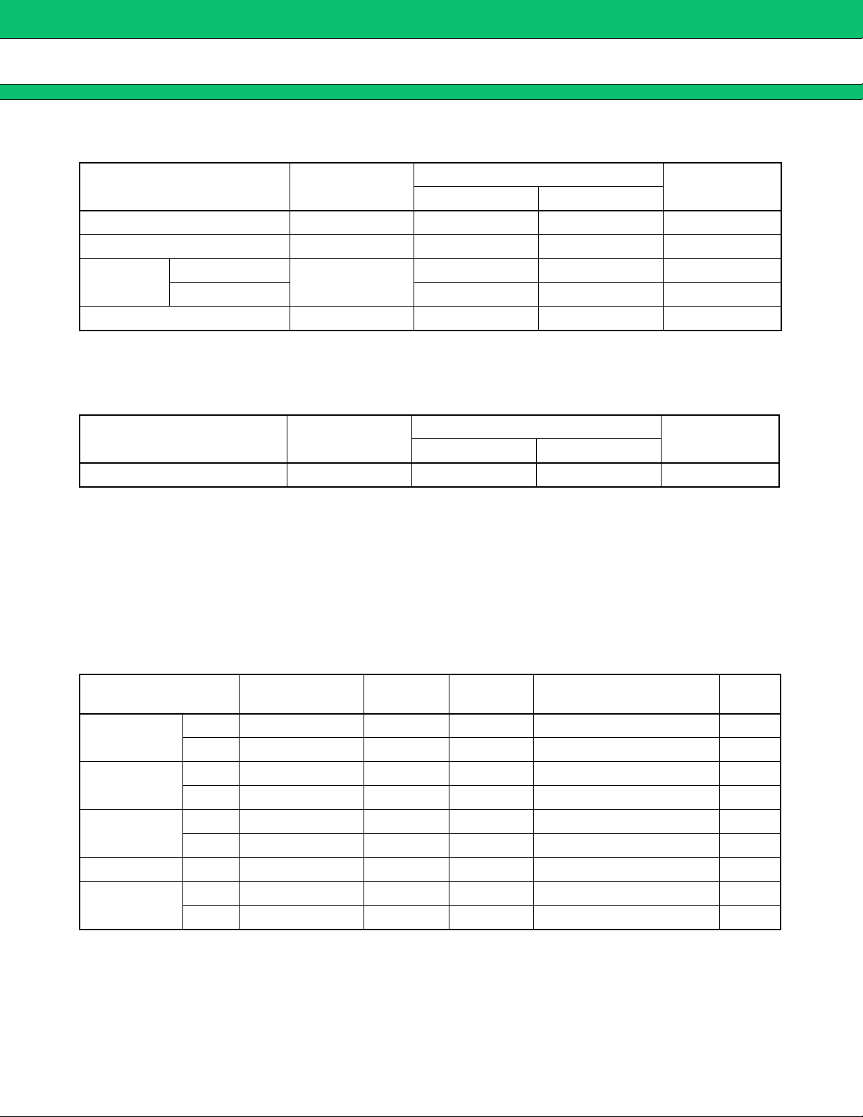
F5CP/F6CP Series
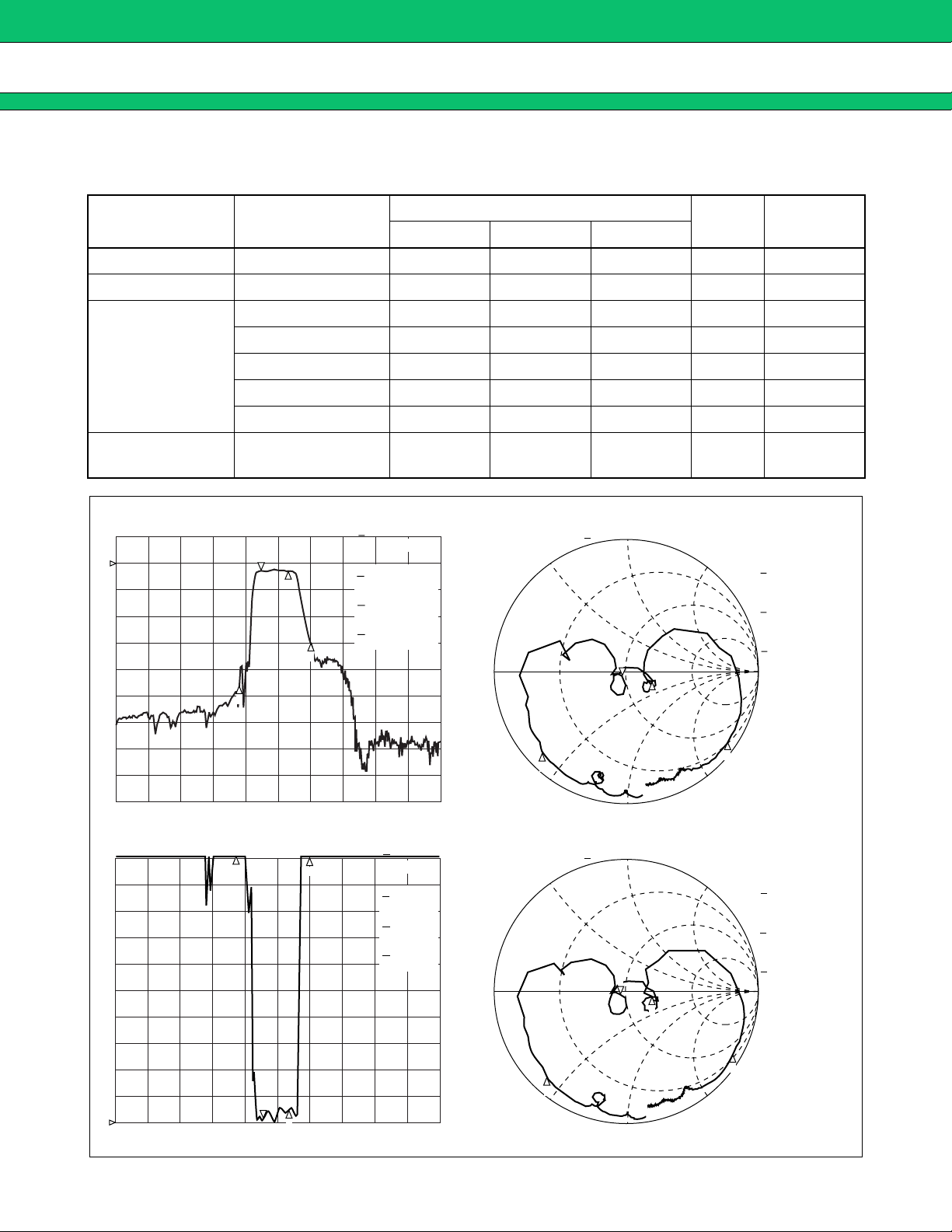
2. PDC800-R
X
PART NUMBER : FAR-F5CP-820M00-D202
Value
Parameter Conditions
Unit Remarks
Min. Typ. Max.
Insertion loss 810 to 830 MHz 2.6 3.3 dB
In-band ripple 810 to 830 MHz 0.8 1.5 dB
DC to 760 MHz 45 52 dB
855 to 875 MHz 28 30 dB
Absolute
attenuation
875 to 920 MHz 35 38 dB
920 to 1200 MHz 45 55 dB
1200 to 2000 MHz 40 47 dB
In-band VSWR
(Return loss)
S21 log MAG 10 dB/ REF 0 dB
810 to 830 MHz
1
1 : −2.4056 dB
2 : −2.5113 dB
2
3 : −56.9 dB
4 : −31.782 dB
4
(8.5)
810 MHz
830 MHz
760 MHz
855 MHz
2.0
(9.5)
11 1U FS 1 : 50.861 Ω−8.7852 Ω
S
2.2
()
1
2
(dB)
22.366 pF
810 MHz
2 : 88.93 Ω
5.2227 Ω
830 MHz
3 : 4.5723 Ω
−48.232 Ω
760 MHz
4 : 22.301 Ω
−121.53 Ω
855 MHz
3
4
SPAN 300 MHz
1 : 1.1966
810 MHz
2 : 1.7897
830 MHz
3 : 21.137
760 MHz
4 : 15.897
855 MHz
CENTER 820 MHz
S11 SWR 1 / REF 1
3
1
CENTER 820 MHz SPAN 300 MHz
2
4
CENTER 820 MHz SPAN 300 MHz
S22 1U FS 1 : 51.545 Ω−8.2246 Ω
CENTER 820 MHz SPAN 300 MHz
3
1
2
4
3
23.89 pF
810 MHz
2 : 86.727 Ω
6.6094 Ω
830 MHz
3 : 4.5059 Ω
−47.348 Ω
760 MHz
4 : 22.906 Ω
−119.41 Ω
855 MHz
5
Page 6
F5CP/F6CP Series
3. SYSTEM : AMPS-Tx
PART NUMBER : FAR-F5CP-836M50-D203
Parameter Conditions
Min. Typ. Max.
Insertion loss 824 to 849 MHz 3.0 3.5 dB
In-band ripple 824 to 849 MHz 1.1 1.6 dB
DC to 800 MHz 45 50 dB
Absolute
attenuation
869 to 1049 MHz 29 35 dB
1049 to 2000 MHz 45 50 dB
Value
Unit Remarks
In-band VSWR
(Return loss)
S21 log MAG 10 dB/ REF 0 dB
CENTER 835 MHz
S11 SWR 1 / REF 1
824 to 849 MHz
1
3
3
(8.5)
1 : −2.8742 dB
824 MHz
4
4
2 : −2.7828 dB
849 MHz
3 : −51.439 dB
800 MHz
4 : −34.045 dB
869 MHz
SPAN 300 MHz
1 : 1.2937
824 MHz
2 : 1.4867
849 MHz
3 : 25.566
800 MHz
4 : 33.367
869 MHz
2
S
CENTER 835 MHz SPAN 300 MHz
S22 1U FS 1 : 38.223 Ω 1.1992 Ω
1.9
(10.2)
11 1U FS 1 : 38.709 Ω 0.1641 Ω
3
2.2
()
1
2
1
2
(dB)
4
31.689 pH
824 MHz
2 : 70.559 Ω
−11.789 Ω
849 MHz
3 : 2.6631 Ω
−30.007 Ω
800 MHz
4 : 13.117 Ω
−138.59 Ω
869 MHz
231.63 pH
824 MHz
2 : 70.09 Ω
−9.5508 Ω
849 MHz
3 : 2.4951 Ω
−30.189 Ω
800 MHz
4 : 13.344 Ω
−140.89 Ω
869 MHz
1
CENTER 835 MHz SPAN 300 MHz
2
6
4
3
CENTER 835 MHz SPAN 300 MHz
Page 7

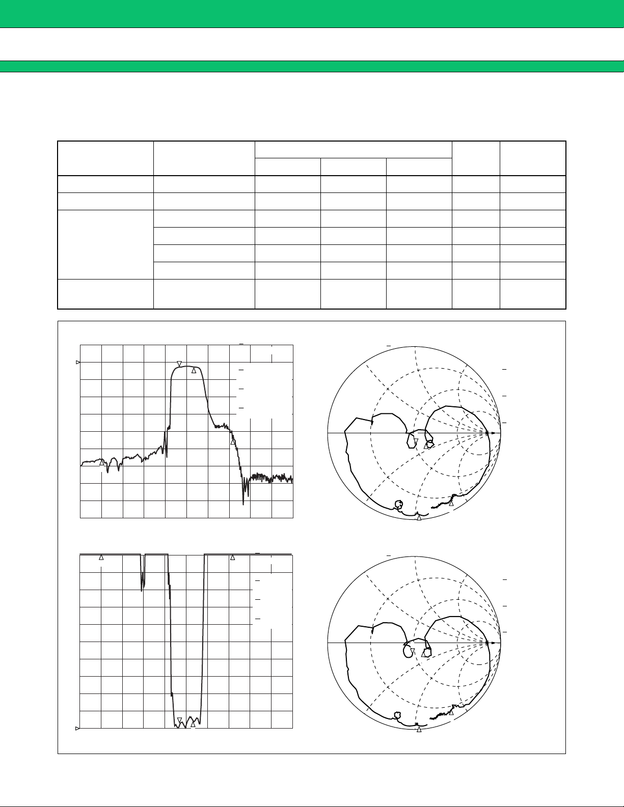
F5CP/F6CP Series
4. SYSTEM : AMPS-Rx
PART NUMBER : FAR-F5CP-881M50-D204
Parameter Conditions
Min. Typ. Max.
Insertion loss 869 to 894 MHz 2.9 3.5 dB
In-band ripple 869 to 894 MHz 1.0 1.6 dB
DC to 779 MHz 45 50 dB
779 to 849 MHz 40 47 dB
Absolute
attenuation
914 to 970 MHz 28 33 dB
970 to 1049 MHz 50 60 dB
1049 to 2000 MHz 40 50 dB
In-band VSWR
(Return loss)
869 to 894 MHz
(8.5)
Value
1.9
(10.2)
2.2
()
Unit Remarks
(dB)
S21 log MAG 10 dB/ REF 0 dB
1
2
4
3
CENTER 880 MHz
S11 SWR 1 / REF 1
3
4
1 : −2.8617 dB
869 MHz
2 : −3.0293 dB
894 MHz
3 : −56.249 dB
849 MHz
4 : −33.517 dB
914 MHz
SPAN 300 MHz
1 : 1.1015
869 MHz
2 : 1.6896
894 MHz
3 : 24.367
849 MHz
4 : 35.586
914 MHz
11 1U FS 1 : 52.887 Ω−4.0195 Ω
S
1
2
3
CENTER 880 MHz SPAN 300 MHz
S22 1U FS
1 : 54.602 Ω
1
2
4
1.627 Ω
45.564 pF
869 MHz
2 : 80.242 Ω
−14.598 Ω
894 MHz
3 : 2.4668 Ω
−22.392 Ω
849 MHz
4 : 12.961 Ω
−142.84 Ω
914 MHz
297.97 pH
869 MHz
2 : 80.621 Ω
−8.7813 Ω
894 MHz
3 : 2.5654 Ω
−22.138 Ω
849 MHz
4 : 15.594 Ω
−156.26 Ω
914 MHz
1
CENTER 880 MHz SPAN 300 MHz
2
4
3
CENTER 880 MHz SPAN 300 MHz
7
Page 8

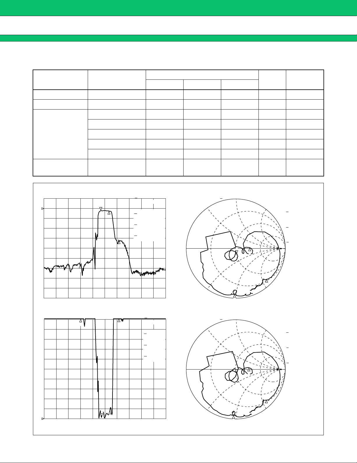
F5CP/F6CP Series
5. SYSTEM : GSM-Tx
PART NUMBER : FAR-F5CP-902M50-D205
Parameter Conditions
Min. Typ. Max.
Insertion loss 890 to 915 MHz 3.0 3.5 dB
In-band ripple 890 to 915 MHz 1.1 1.6 dB
DC to 845 MHz 45 50 dB
845 to 870 MHz 30 46 dB
Absolute
attenuation
925 to 935 MHz 7 16 dB
935 to 980 MHz 28 33 dB
980 to 1200 MHz 50 60 dB
1200 to 3000 MHz 30 40 dB
Value
Unit Remarks
In-Band VSWR
(Return loss)
S21 log MAG 10 dB/ REF 0 dB
CENTER 900 MHz
S11 SWR 1 / REF 1
890 to 915 MHz
1
3
3
(9.0)
1 : −2.7524 dB
890 MHz
5
5
2 : −2.6529 dB
915 MHz
3 : −55.923 dB
870 MHz
4 : −14.643 dB
925 MHz
5 : −32.307 dB
935 MHz
SPAN 300 MHz
1 : 1.2064
890 MHz
2 : 1.584
915 MHz
3 : 21.644
870 MHz
4 : 13.206
925 MHz
5 : 29.787
935 MHz
CENTER 900 MHz SPAN 300 MHz
2
4
4
1.7
(11.7)
S11 1U FS 1 : 41.604 Ω−1.2832 Ω
3
S22 1U FS 1 : 40.996 Ω−1.9941 Ω
1
1
2.1
()
(dB)
2
2
4
5
4
139.36 pF
890 MHz
2 : 77.059 Ω
−9.8828 Ω
915 MHz
3 : 2.9404 Ω
−26.104 Ω
870 MHz
4 : 446.91 Ω
298.7 Ω
925 MHz
5 : 18.18 Ω
−155.7 Ω
935 MHz
89.676 pF
890 MHz
2 : 77.371 Ω
−7.6758 Ω
915 MHz
3 : 3.0254 Ω
−25.578 Ω
870 MHz
4 : 502.38 Ω
264.7 Ω
925 MHz
5 : 17.695 Ω
−150.65 Ω
935 MHz
1
CENTER 900 MHz SPAN 300 MHz
2
8
5
3
CENTER 900 MHz SPAN 300 MHz
Page 9
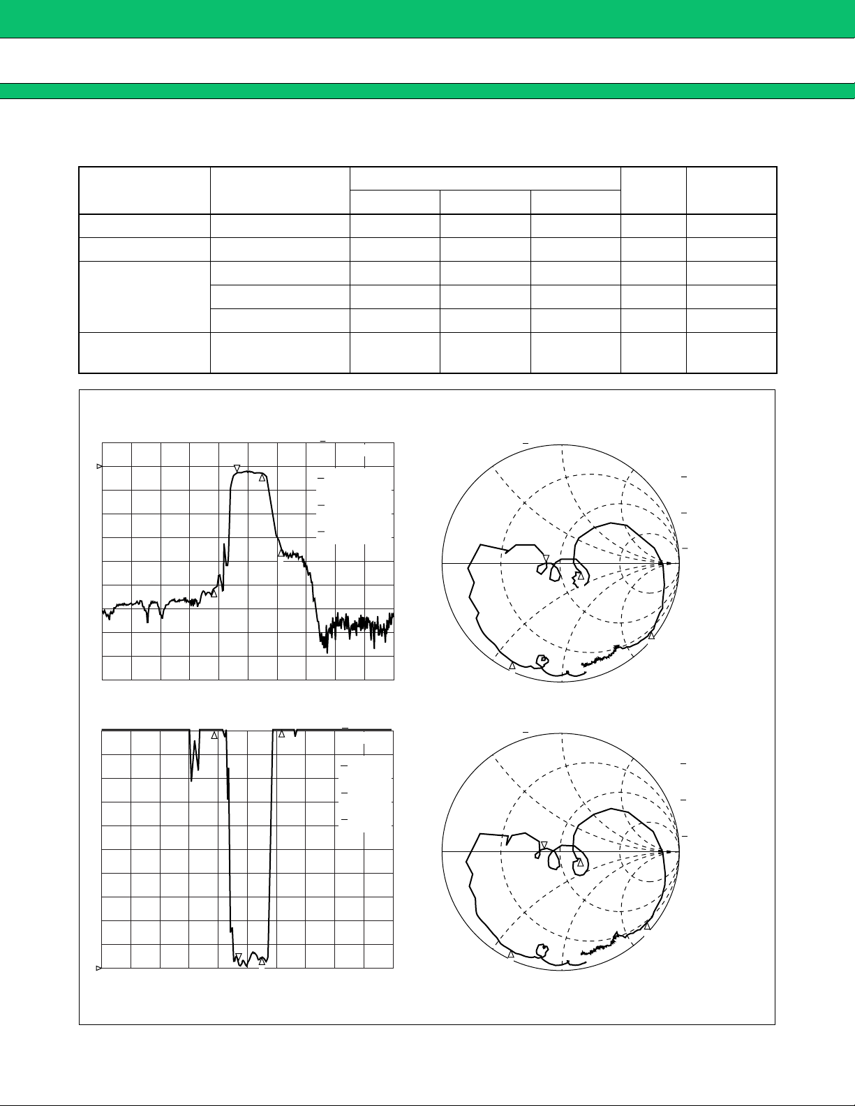
F5CP/F6CP Series
6. SYSTEM : GSM-Rx
PART NUMBER : FAR-F5CP-947M50-D206
Parameter Conditions
Min. Typ. Max.
Insertion loss 935 to 960 MHz 3.1 3.5 dB
In-band ripple 935 to 960 MHz 1.3 1.5 dB
DC to 871 MHz 45 50 dB
890 to 915 MHz 30 45 dB
Absolute
attenuation
980 to 1025 MHz 25 30 dB
1025 to 2000 MHz 45 48 dB
2000 to 3000 MHz 30 33 dB
In-band VSWR
(Return loss)
935 to 960 MHz
(8.1)
Value
2.1
(9.0)
2.3
()
Unit Remarks
(dB)
S21 log MAG 10 dB/ REF 0 dB
1
2
4
3
CENTER 950 MHz
S11 SWR 1 / REF 1
3
4
1 : −2.9325 dB
935 MHz
2 : −2.8297 dB
960 MHz
3 : −45.716 dB
915 MHz
4 : −30.562 dB
980 MHz
SPAN 300 MHz
1 : 1.1193
935 MHz
2 : 1.5219
960 MHz
3 : 18.194
915 MHz
4 : 30.704
980 MHz
S11 1U FS 1 : 46.617 Ω−4.2656 Ω
1
2
3
CENTER 950 MHz SPAN 300 MHz
S22 1U FS 1 : 47.164 Ω−1.9922 Ω
1
2
4
39.905 pF
935 MHz
2 : 72.273 Ω
−12.234 Ω
960 MHz
3 : 3.1875 Ω
−19.772 Ω
915 MHz
4 : 18.07 Ω
−157.97 Ω
980 MHz
85.443 pF
935 MHz
2 : 72.879 Ω
−7.1406 Ω
960 MHz
3 : 3.4033 Ω
−19.452 Ω
915 MHz
4 : 20.859 Ω
−170.99 Ω
980 MHz
1
CENTER 950 MHz SPAN 300 MHz
2
4
3
CENTER 950 MHz SPAN 300 MHz
9
Page 10

F5CP/F6CP Series
7. SYSTEM : EGSM-Rx
PART NUMBER : FAR-F5CP-942M50-D201
Parameter Conditions
Min. Typ. Max.
Insertion loss 925 to 960 MHz 3.9 4.8 dB
In-band ripple 925 to 960 MHz 2.0 2.9 dB
DC to 871 MHz 45 53 dB
890 to 915 MHz 15 20 dB
Absolute
attenuation
980 to 1025 MHz 25 29 dB
1025 to 2000 MHz 40 50 dB
2000 to 3000 MHz 25 36 dB
In-band VSWR
(Return loss)
925 to 960 MHz
(6.0)
Value
2.4
(7.7)
3.0
()
Unit Remarks
(dB)
S21 log MAG 10 dB/ REF 0 dB
1
2
3
CENTER 950 MHz
S11 SWR 1 / REF 1
3
4
4
1 : −3.8751 dB
925 MHz
2 : −2.9443 dB
960 MHz
3 : −33.524 dB
915 MHz
4 : −32.697 dB
980 MHz
SPAN 300 MHz
1 : 2.1506
925 MHz
2 : 1.1932
960 MHz
3 : 7.4697
915 MHz
4 : 30.348
980 MHz
11 1U FS 1 : 24.956 Ω−11.556 Ω
S
1
3
CENTER 950 MHz SPAN 300 MHz
S22 1U FS 1 : 25.901 Ω−15.088 Ω
2
4
1
2
14.89 pF
925 MHz
2 : 59.1 Ω
−2.7793 Ω
960 MHz
3 : 7.0146 Ω
−10.637 Ω
915 MHz
4 : 15.141 Ω
−142.4 Ω
980 MHz
11.404 pF
925 MHz
2 : 56.229 Ω
−7.6113 Ω
960 MHz
3 : 8.3276 Ω
−8.667 Ω
915 MHz
4 : 13.266 Ω
−131.7 Ω
980 MHz
10
1
CENTER 950 MHz SPAN 300 MHz
2
3
4
CENTER 950 MHz SPAN 300 MHz
Page 11

F5CP/F6CP Series
8. SYSTEM : PDC1.5G-Tx
PART NUMBER : FAR-F6CP-1G4410-D207
Parameter Conditions
Min. Typ. Max.
Insertion loss 1429 to 1453 MHz 3.5 3.8 dB
In-band ripple 1429 to 1453 MHz 1.3 1.6 dB
DC to 1380 MHz 40 45 dB
1477 to 1501 MHz 25 28 dB
Absolute
attenuation
1501 to 1607 MHz 28 30 dB
1607 to 1900 MHz 45 55 dB
1900 to 3000 MHz 30 33 dB
In-band VSWR
(Return loss)
1429 to 1453 MHz
(7.0)
Value
2.4
(7.7)
2.6
()
Unit Remarks
(dB)
S21 log MAG 10 dB/ REF 0 dB
1
2
4
3
CENTER 1 450 MHz
S11 SWR 1 / REF 1
3
4
1 : −2.6466 dB
1.429 GHz
2 : −2.8931 dB
1.453 GHz
3 : −48.237 dB
1.38 GHz
4 : −30.021 dB
1.477 GHz
5 : −61.614 dB
1.607 GHz
5
SPAN 400 MHz
5
1 : 1.2523
1.429 GHz
2 : 1.4666
1.453 GHz
3 : 15.581
1.38 GHz
4 : 26.309
1.477 GHz
5 : 15.408
1.607 GHz
S11 1U FS 1 : 39.924 Ω 0.0859 Ω
2 : 66.582 Ω
3 : 3.9805 Ω
1
2
3
CENTER 1 450 MHz SPAN 400 MHz
S22 1U FS 1 : 39.836 Ω 0.4395 Ω
5
1
2
4
4 : 15.57 Ω
5 : 7.3418 Ω
2 : 67.617 Ω
3 : 4.1484 Ω
4 : 23.188 Ω
5 : 8.541 Ω
9.5712 pH
1.429 GHz
−14.813 Ω
1.453 GHz
−24.466 Ω
1.38 GHz
−133.34 Ω
1.477 GHz
−55.936 Ω
1.607 GHz
48.944 pH
1.429 GHz
−12.059 Ω
1.453 GHz
−25.398 Ω
1.38 GHz
−166.48 Ω
1.477 GHz
−61.674 Ω
1.607 GHz
1
CENTER 1 450 MHz SPAN 400 MHz
2
4
3
5
CENTER 1 450 MHz SPAN 400 MHz
11
Page 12

F5CP/F6CP Series
9. SYSTEM : PDC1.5G-Rx
PART NUMBER : FAR-F6CP-1G4890-D208
Parameter Conditions
Min. Typ. Max.
Insertion loss 1477 to 1501 MHz 3.6 4.0 dB
In-band ripple 1477 to 1501 MHz 1.3 1.7 dB
DC to 1370 MHz 45 50 dB
1370 to 1429 MHz 40 45 dB
1429 to 1453 MHz 15 30 dB
Absolute
attenuation
1542 to 1566 MHz 28 30 dB
1566 to 1607 MHz 28 30 dB
1607 to 1900 MHz 40 45 dB
1900 to 3000 MHz 30 35 dB
In-band VSWR
(Return loss)
1477 to 1501 MHz
(6.8)
Value
2.5
(7.4)
2.7
()
Unit Remarks
(dB)
S21 log MAG 10 dB/ REF 0 dB
1
2
4
3
CENTER 1 500 MHz
S11 SWR 1 / REF 1
4 5
3
1 : −3.367 dB
1.477 GHz
2 : −3.1358 dB
1.501 GHz
3 : −44.243 dB
1.453 GHz
4 : −35.072 dB
1.542 GHz
5 : −64.128 dB
1.607 GHz
5
SPAN 400 MHz
1 : 1.5913
1.477 GHz
2 : 1.7639
1.501 GHz
3 : 6.6353
1.453 GHz
4 : 29.248
1.542 GHz
5 : 19.199
1.607 GHz
S11 1U FS 1 : 39.094 Ω−17.623 Ω
1
3
CENTER 1 500 MHz SPAN 400 MHz
S22 1U FS 1 : 42.766 Ω−19.346 Ω
3
2
4
5
1
2
6.1145 pF
1.477 GHz
2 : 52.408 Ω
−29.346 Ω
1.501 GHz
3 : 7.6753 Ω
−6.7566 Ω
1.453 GHz
4 : 10.273 Ω
−111.5 Ω
1.542 GHz
5 : 7.4102 Ω
−67.687 Ω
1.607 GHz
5.57 pF
1.477 GHz
2 : 54.113 Ω
−28.582 Ω
1.501 GHz
3 : 7.5981 Ω
−7.1064 Ω
1.453 GHz
4 : 12.152 Ω
−125.3 Ω
1.542 GHz
5 : 8.4102 Ω
−73.254 Ω
1.607 GHz
1
2
CENTER 1 500 MHz SPAN 400 MHz
12
4
5
CENTER 1 500 MHz SPAN 400 MHz
Page 13

MEASUREMENT CIRCUIT
■■■■
Network Analyzer Network Analyzer
F5CP/F6CP Series
13
50 Ω 50 Ω
PART NUMBER DESIGNATION
■■■■
[Designation example]
FAR-F5CP-
(2)
(1) (3) (4) (5)
(1) Frequency range 5 : 700 to 1000 MHz
6 : 1000 to 1700 MHz
(2) Package size P : 2.5 mm × 2.0 mm × 0.9 mm
(3) Frequency This specifies the nominal center frequency using six alphanumeric.
M (for MHz) or G (for GHz) indicates the decimal point.
[Example] 836.5 MHz → 836M50
(4) Part symbol Numbers specified by Fujitsu
Refer to STANDARD DEVICES
(5) Packing (Reeled tape) W : 1000 pcs / reel
V : 3000 pcs / reel
U : 5000 pcs / reel
-D2 -
1.441 GHz → 1G4410
Filter
2, 4
1 to 4 : Pin numbers
MARKING
■■■■
Production date (EIAJ)
Lot CodePart symbol
INDEX
13
Page 14

F5CP/F6CP Series
PACKAGE DIMENSIONS
■■■■
0.9 ± 0.10
2.5 ± 0.10
2.0 ± 0.10
4 − R0.18
RECOMMENDED FOOT PATTERN ON PCB
■■■■
3
2
0.88 ± 0.10
(C 030)
INDEX
0.5 Min.
4
0.63 ± 0.10
1
Dimensions in mm.
0.5 Min.
14
0.5
1.2 0.5
0.88
0.5
0.88
1.20.8
Dimensions in mm.
Page 15

PACKING
■■■■
(1) Reel dimensions
φ13.0 ± 0.2
2.0 ± 0.5
φ21.0 ± 0.8
R0.1
F5CP/F6CP Series
φ80.0
φ250.0
Type Volume
W 1000 pcs.
V 3000 pcs.
U 5000 pcs.
(2) Packing style
Pulling side
12.4
18.4 Max.
Reel side
+2.0
−0.0
Dimensions in mm.
Pulling side
15
Page 16

F5CP/F6CP Series
(3) Tape dimensions
1.5 ± 0.1
2.8
2.3
2.0 ± 0.1 4.0 ± 0.1
1.5 ± 0.1
(4) Peel strength of top cover tape
Peel off by the force of 0.1 N to 0.7 N under the
condition at the right .
(Conforms to JIS C 0806 section 5.2)
4.0 ± 0.1
0.3 ± 0.05
5.5 ± 0.1 1.75 ± 0.1
12.0 ± 0.2
1.0 ± 0.1
Dimensions in mm.
Direction of pulling
Speed 300 mm/min
16
165 to 180 °
Embossment carrier type tape
Page 17

RECOMMENDED REFLOW PROFILE
■■■■
F5CP/F6CP Series
240
Heating rate
1 to 4 °C/s
210
■■■■
Temperature (°C)
150
NOTE
Pre-Heating
60 ∼ 90 s
Time (s)
Mass-produced product order is accepted by a unit of 1000.
10 s
Air cooling
60 s
17
Page 18

F5CP/F6CP Series
FUJITSU MEDIA DEVICES LIMITED
For further information please contact:
Japan
FUJITSU MEDIA DEVICE LIMITED
International Sales & Marketing DEPT.
Shin-Yokohama Square Bldg.,14F,
Shin-yokohama 2-3-12,
Kohoku-ku , Yokohama,
Kanagawa 222-0033, Japan
Tel: +81-45-471-0061
Fax: +81-45-471-0076
http://www.fujitsu.co.jp/hypertext/fmd/English/index.html
North and South America
FUJITSU MICROELECTRONICS, INC.
3545 North First Street,
San Jose, CA 95134-1804, U.S.A.
Tel: +1-408-922-9000
Fax: +1-408-922-9179
Customer Response Center
Mon. - Fri.: 7 am - 5 pm (PST)
Tel: +1-800-866-8608
Fax: +1-408-922-9179
http://www.fujitsumicro.com/
Europe
FUJITSU MICROELECTRONICS EUR OPE GmbH
Am Siebenstein 6-10,
D-63303 Dreieich-Buchschlag,
Germany
Tel: +49-6103-690-0
Fax: +49-6103-690-122
http://www.fujitsu-fme.com/
Asia Pacific
FUJITSU MICROELECTRONICS ASIA PTE. LTD.
#05-08, 151 Lorong Chuan,
New Tech Park,
Singapore 556741
Tel: +65-281-0770
Fax: +65-281-0220
http://www.fmap.com.sg/
All Rights Reserved.
The contents of this document are subject to change without notice.
Customers are advised to consult with FUJITSU sales
representatives before ordering.
The information and circuit diagrams in this document are
presented as examples of semiconductor device applications, and
are not intended to be incorporated in devices for actual use. Also,
FUJITSU is unable to assume responsibility for infringement of
any patent rights or other rights of third parties arising from the use
of this information or circuit diagrams.
The contents of this document may not be reproduced or copied
without the permission of FUJITSU LIMITED.
FUJITSU semiconductor devices are intended for use in standard
applications (computers, office automation and other office
equipments, industrial, communications, and measurement
equipments, personal or household devices, etc.).
CAUTION:
Customers considering the use of our products in special
applications where failure or abnormal operation may directly
affect human lives or cause physical injury or property damage, or
where extremely high levels of reliability are demanded (such as
aerospace systems, atomic energy controls, sea floor repeaters,
vehicle operating controls, medical devices for life support, etc.)
are requested to consult with FUJITSU sales representatives before
such use. The company will not be responsible for damages arising
from such use without prior approval.
Any semiconductor devices have inherently a certain rate of failure.
You must protect against injury, damage or loss from such failures
by incorporating safety design measures into your facility and
equipment such as redundancy, fire protection, and prevention of
over-current levels and other abnormal operating conditions.
If any products described in this document represent goods or
technologies subject to certain restrictions on export under the
Foreign Exchange and Foreign Trade Control Law of Japan, the
prior authorization by Japanese government should be required for
export of those products from Japan.
F0012
FUJITSU LIMITED Printed in Japan
Page 19

Copyright © Each Manufacturing Company.
All Datasheets cannot be modified without permission.
This datasheet has been download from :
www.AllDataSheet.com
100% Free DataSheet Search Site.
Free Download.
No Register.
Fast Search System.
www.AllDataSheet.com
 Loading...