

Page 1

FUJITSU SEMICONDUCTOR
CONTROLLER MANUAL
CM44-10136-1E
TM
F2MC
16-BIT MICROCONTROLLER
-16LX
MB90360 Series
HARDWARE MANUAL
Page 2

Page 3

TM
F2MC
16-BIT MICROCONTROLLER
-16LX
MB90360 Series
HARDWARE MANUAL
FUJITSU LIMITED
Page 4

Page 5

PREFACE
■ Objectives and intended reader
Thank you very much for your continued patronage of Fujitsu semiconductor products.
The MB90360 series has b een developed as a ge neral-purpose version of the F
which is an original 16-bit single-chip microcontroller compatible with the Application Specific IC
(ASIC).
This manual explains the functions and operation of the MB90360 series for engineers who actually
use the MB90360 series to design products. Please read this manual first.
■ Tr ademark
2
F
MC, an abbreviation of FUJIT SU Flexible Microco ntroller, is a registered trademark of FUJITSU
Ltd.
Embedded Algorithm is a registered trademark of Advanced Micro Devices Inc.
■ Structure of this preliminary manual
This manual contains the following 26 chapters and appendix.
2
MC-16LX family,
CHAPTER 1 OVERVIEW
2
The MB90360 Series is a family member of the F
CHAPTER 2 CPU
This chapter explains the CPU.
CHAPTER 3 INTERRUPTS
This chapter explains the interrupts and function and op eration of the extended intelligent I/O
service in the MB90360 series.
CHAPTER 4 DELAYED INTERRUPT GENERATION MODULE
This chapter explains the functions and operations of the delayed interrupt generation module.
CHAPTER 5 CLOCKS
This chapter explains the clocks used by MB90360 series microcontrollers.
CHAPTER 6 CLOCK SUPERVISOR
This chapter explain s the function and the operation of the cloc k supervisor. Only the product
with built-in clock supervisor of the MB90360 series is valid to this function.
CHAPTER 7 RESETS
This chapter describes resets for the MB90360-series microcontrollers.
CHAPTER 8 LOW-POWER CONSUMPTION MODE
MC-16LX micro controllers.
This chapter explains the low-power consumption mode of MB90360 series microcontrollers.
CHAPTER 9 MEMORY ACCESS MODES
This chapter explains the functions and operations of the memory access modes.
i
Page 6

CHAPTER 10 I/O PORTS
This chapter explains the functions and operations of the I/O ports.
CHAPTER 11 TIMEBASE TIMER
This chapter explains the functions and operations of the timebase timer.
CHAPTER 12 WATCHDOG TIMER
This chapter describes the function and operation of the watchdog timer.
CHAPTER 13 16-Bit I/O TIMER
This chapter explains the function and operation of the 16- bit I/O timer.
CHAPTER 14 16-BIT RELOAD TIMER
This chapter describes the functions and operation of the 16-bit reload timer.
CHAPTER 15 WATCH TIMER
This chapter describes the functions and operations of the watch timer.
CHAPTER 16 8-/16-BIT PPG TIMER
This chapter describes the functions and operations of the 8-/16-bit PPG timer.
CHAPTER 17 DTP/EXTERNAL INTERRUPTS
This chapter explains the functions and operations of DTP/external interrupt.
CHAPTER 18 8-/10-BIT A/D CONVERTER
This chapter explains the functions and operation of 8-/10-bit A/D converter.
CHAPTER 19 LOW VOLTAGE DETECTION/CPU OPERATING DETECTION RESET
This chapter explains the function and operating the low voltage detection/CPU operating
detection reset. This function can use only the product with "T" suffix of MB90360 series.
CHAPTER 20 LIN-UART
This chapter explains the functions and operation of LIN-UART.
CHAPTER 21 CAN CONTROLLER
This chapter explains the functions and operations of the CAN controller.
CHAPTER 22 ADDRESS MATCH DETECTION FUNCTION
This chapter explains the address match detection function and its operation.
CHAPTER 23 ROM MIRRORING MODULE
This chapter describes the functions and operations of the ROM mirroring function select
module.
CHAPTER 24 512K-BIT FLASH MEMORY
This chapter explains the functions and operation of the 512K-bit flash mem ory. The following
three methods are available for writing data to and erasing data from the flash memory:
• Parallel programmer
• Serial programmer
• Executing programs to write/erase data
This chapter explains “Executing programs to write/erase data”.
ii
Page 7

CHAPTER 25 EXAMPLES OF MB90F362/T(S), MB90F367/T(S) SERIAL PROGRAMMING
CONNECTION
This chapter shows an examp le of a serial programming connection using the AF220/AF210/
AF120/AF110 Flas h Micro-computer Programmer by Yo kogawa Digital Computer Corporation
when the AF220/AF210/AF120/AF110 flash serial microcontroller programer from Yokogawa
Digital Computer Corporation is used.
CHAPTER 26 ROM SECURITY FUNCTION
This chapter explains the ROM security function.
APPENDIX
The appendixes provide I/O maps, instructions, and other information.
iii
Page 8

• The contents of this document are subject to change without notice.
Customers are advised to consult with FUJITSU sales representatives before ordering.
• The information, such as descriptions of function and application circuit examples, in this document are
presented solely for the purpose of reference to show examples of operations and uses of Fujitsu
semiconductor device; Fujitsu does not warrant proper operation of the device with respect to use based
on such information. When you develop equipment incorporating the device based on such information,
you must assume any responsibility arising out of such use of the information. Fujitsu assumes no
liability for any damages whatsoever arising out of the use of the information.
• Any information in this document, including descriptions of function and schematic diagrams, shall not be
construed as license of the use or exercise of any intellectual property right, such as patent right or
copyright, or any other right of Fujitsu or any third party or does Fujitsu warrant non-infringement of any
third-party' s intellectual property right or other right by using such information. Fujitsu assumes no
liability for any infringement of the intellectual property rights or other rights of third parties which would
result from the use of information contained herein.
• The products described in this document are designed, developed and manufactured as contemplated
for general use, including without limitation, ordinary industrial use, general office use, personal use, and
household use, but are not designed, developed and manufactured as contemplated (1) for use
accompanying fatal risks or dangers that, unless extremely high safety is secured, could have a serious
effect to the public, and could lead directly to death, personal injury, severe physical damage or other
loss (i.e., nuclear reaction control in nuclear facility, aircraft flight control, air traffic control, mass
transport control, medical life support system, missile launch control in weapon system), or (2) for use
requiring extremely high reliability (i.e., submersible repeater and artificial satellite).
Please note that Fujitsu will not be liable against you and/or any third party for any claims or damages
arising in connection with above- mentioned uses of the products.
• Any semiconductor devices have an inherent chance of failure. You must protect against injury, damage
or loss from such failures by incorporating safety design measures into your facility and equipment such
as redundancy, fire protection, and prevention of over-current levels and other abnormal operating
conditions.
• If any products described in this document represent goods or technologies subject to certain restrictions
on export under the Foreign Exchange and Foreign Trade Law of Japan, the prior authorization by
Japanese government will be required for export of those products from Japan.
©2005 FUJITSU LIMITED Printed in Japan
iv
Page 9

CONTENTS
CHAPTER 1 OVERVIEW ................................................................................................... 1
1.1 Overview of MB90360 ........................................................................................................................ 2
1.2 Block Diagram of MB90360 series ..................................................................................................... 9
1.3 Package Dimensions ........................................................................................................................ 12
1.4 Pin Assignment ................................................................................................................................ . 13
1.5 Pin Functions ................................................................................................................ .................... 14
1.6 Input-Output Circuits ......................................................................................................................... 17
1.7 Handling Device .................................................. ....... ...... ...... ....... ...... ....... ...... ....... .......................... 21
CHAPTER 2 CPU ............................................................................................................ 27
2.1 Outline of the CPU ..................................................................................................................... ....... 28
2.2 Memory Space ..................................................................................................................... ...... ....... 29
2.3 Memory Map ..................................................................................................................................... 32
2.4 Linear Addressing ............................................................................................................................. 33
2.5 Bank Addressing Types .................................................................................................................... 34
2.6 Multi-byte Data in Memory Space ..................................................................................................... 36
2.7 Registers ................ ...... ....... ...... ....... ...... ....... ...... ....... ...... ...... ....................................... ....... ...... ....... 37
2.7.1 Accumulator (A) .................................................................................................................... ....... 40
2.7.2 User Stack Pointer (USP) and System Stack Pointer (SSP) ....................................................... 41
2.7.3 Processor Status (PS) ................................................................................................................. 42
2.7.4 Program Counter (PC) ................................................................................................................. 45
2.8 Register Bank ............................................................................................................... ....... ...... ....... 46
2.9 Prefix Codes ........................................................................................................................ ...... ....... 48
2.10 Interrupt Disable Instructions ............................................................................................................ 51
2.11 Precautions for Use of "DIV A, Ri" and "DIVW A, RWi" Instructions ................................................ 52
CHAPTER 3 INTERRUPTS ............................................................................................. 55
3.1 Outline of Interrupts .......................................................................................................................... 56
3.2 Interrupt Vector ................................................................................................................................. 59
3.3 Interrupt Control Registers (ICR) ...................................................................................................... 61
3.4 Interrupt Flow .................................................................................................................................... 65
3.5 Hardware Interrupts .......................................................................................................................... 67
3.5.1 Hardware Interrupt Operation ...................................................................................................... 68
3.5.2 Occurrence and Release of Hardware Interrupt .......................................................................... 69
3.5.3 Multiple interrupts ........................................................................................................................ 71
3.6 Software Interrupts ................... ....................................... ...... ....... ...... ....... ...... ....... ...... ....... ...... ....... 72
3.7 Extended Intelligent I/O Service (EI
3.7.1 Extended Intelligent I/O Service Descriptor (ISD) ....................................................................... 76
3.7.2 EI
3.8 Operation Flow of and Procedure for Using the Extended Intelligent I/O Service (EI
3.9 Exceptions ........................................................................................................................................ 82
2
OS Status Register (ISCS) ..................................................................................................... 78
2
OS) ............................... .............................................. ............. 74
2
OS) .............. 79
v
Page 10

CHAPTER 4 DELAYED INTERRUPT GENERATION MODULE .................................... 83
4.1 Overview of Delayed Interrupt Generation Module ........................................................................... 84
4.2 Block Diagram of Delayed Interrupt Generation Module .................................................................. 85
4.3 Configuration of Delayed Interrupt Generation Module .................................................................... 86
4.3.1 Delayed interrupt request generate/cancel register (DIRR) ........................................................ 87
4.4 Explanation of Operation of Delayed Interrupt Generation Module .................................................. 88
4.5 Precautions when Using Delayed Interrupt Generation Module ....................................................... 89
4.6 Program Example of Delayed Interrupt Generation Module ............................................................. 90
CHAPTER 5 CLOCKS ..................................................................................................... 91
5.1 Clocks .................... ....................................................................... .................................................... 92
5.2 Block Diagram of the Clock Generation Block .................................................................................. 95
5.2.1 Register of Clock Generation Block ............................................................................................. 97
5.3 Clock Selection Register (CKSCR) ................................................................................................... 98
5.4 PLL/Subclock Control Register (PSCCR) ....................................................................................... 101
5.5 Clock Mode ..................................................................................................................................... 103
5.6 Oscillation Stabilization Wait Interval .............................................................................................. 107
5.7 Connection of an Oscillator or an External Clock to the Microcontroller ......................................... 108
CHAPTER 6 CLOCK SUPERVISOR ............................................................................. 109
6.1 Overview of Clock Supervisor ......................................................................................................... 110
6.2 Block Diagram of Clock Supervisor ................................................................................................ 111
6.3 Clock Supervisor Control Register (CSVCR) .................................................................................. 113
6.4 Operating Mode of Clock Supervisor .............................................................................................. 115
CHAPTER 7 RESETS .................................................................................................... 119
7.1 Resets .......................... ............. ............. ............. ....... ............ ............. ............. ............................... 120
7.2 Reset Cause and Oscillation Stabilization Wait Times ................................................................... 123
7.3 External Reset Pin .......................................................................................................................... 125
7.4 Reset Operation .................. ...... ....... ...................................... ....... ...... ....... ...... ....... ........................ 126
7.5 Reset Cause Bits ... ...... ....... ....................................... ...... ...... ....... ...... ....... ...... ....... ...... .................. 128
7.6 Status of Pins in a Reset ................................................................................................................ 132
CHAPTER 8 LOW-POWER CONSUMPTION MODE ................................................... 133
8.1 Overview of Low-Power Consumption Mode .................................................................................. 134
8.2 Block Diagram of the Low-Power Consumption Control Circuit ..................................................... 137
8.3 Low-Power Consumption Mode Control Register (LPMCR) ........................................................... 139
8.4 CPU Intermittent Operation Mode .................................................................................................. 142
8.5 Standby Mode .............. ....... ...... ....... ...... ....... ...... ....... ...... ...... ....... .................................................. 143
8.5.1 Sleep Mode ............................................................................................................................... 145
8.5.2 Watch Mode .............................................................................................................................. 148
8.5.3 Timebase Timer Mode ............................................................................................................... 150
8.5.4 Stop Mode ................................................................................................................................. 152
8.6 Status Change Diagram ................................................................................................................. 155
8.7 Status of Pins in Standby Mode and during Hold and Reset .......................................................... 156
8.8 Usage Notes on Low-Power Consumption Mode ........................................................................... 157
vi
Page 11

CHAPTER 9 MEMORY ACCESS MODES .................................................................... 161
9.1 Outline of Memory Access Modes .................................................................................................. 162
9.1.1 Mode Pins .................................................................................................................................. 163
9.1.2 Mode Data ................................................................................................................................. 164
9.1.3 Memory Space in Each Bus Mode ............................................................................................ 165
CHAPTER 10 I/O PORTS ................................................................................................ 167
10.1 I/O Ports .......................................................................................................................................... 168
10.2 I/O Port Registers ........................................................................................................................... 169
10.2.1 Port Data Register (PDR) .......................................................................................................... 170
10.2.2 Port Direction Register (DDR) ................................................................................................... 172
10.2.3 Pull-up Control Register (PUCR) ............................................................................................... 174
10.2.4 Analog Input Enable Register (ADER) ...................................................................................... 175
10.2.5 Input Level Select Register ........................................................................................................ 176
CHAPTER 11 TIMEBASE TIMER ................................................................................... 179
11.1 Overview of Timebase Timer .......................................................................................................... 180
11.2 Block Diagram of Timebase Timer ................................................................................................. 182
11.3 Configuration of Timebase Timer ................................................................................................... 184
11.3.1 Timebase timer control register (TBTC) .................................................................................... 185
11.4 Interrupt of Timebase Timer ........................................................................................................... 187
11.5 Explanation of Operations of Timebase Timer Functions ............................................................... 188
11.6 Precautions when Using Timebase Timer ...................................................................................... 192
11.7 Program Example of Timebase Timer ............................................................................................ 193
CHAPTER 12 WATCHDOG TIMER ................................................................................ 195
12.1 Overview of Watchdog Timer ......................................................................................................... 196
12.2 Configuration of Watchdog Timer ................................................................................................... 199
12.3 Watchdog Timer Registers ............................................................................................................. 201
12.3.1 Watchdog timer control register (WDTC) .................................................................................. 202
12.4 Explanation of Operations of Watchdog Timer Functions .............................................................. 204
12.5 Precautions when Using Watchdog Timer ...................................................................................... 207
12.6 Program Examples of Watchdog Timer .......................................................................................... 208
CHAPTER 13 16-Bit I/O TIMER ............................................................ ..... ..... .... ............ 209
13.1 Overview of 16-bit I/O Timer ........................................................................................................... 210
13.2 Block Diagram of 16-bit I/O Timer .................................................................................................. 211
13.2.1 Block Diagram of 16-bit Free-run Timer .................................................................................... 213
13.2.2 Block Diagram of Input Capture ................................................................................................ 214
13.3 Configuration of 16-bit I/O Timer .................................................................................................... 216
13.3.1 Timer Control Status Register (Upper) (TCCSH) ...................................................................... 217
13.3.2 Timer Control Status Register (Lower) (TCCSL) ....................................................................... 218
13.3.3 Timer Data Register (TCDT) ..................................................................................................... 220
13.3.4 Input Capture Control Status Registers (ICS) ........................................................................... 221
13.3.5 Input Capture Register (IPCP) ................................................................................................... 223
13.3.6 Input Capture Edge Register (ICE) ............................................................................................ 224
13.4 Interrupts of 16-bit I/O Timer ........................................................................................................... 227
vii
Page 12

13.5 Explanation of Operation of 16-bit Free-run Timer ......................................................................... 229
13.6 Explanation of Operation of Input Capture ..................................................................................... 231
13.7 Precautions when Using 16-bit I/O Timer ....................................................................................... 233
13.8 Program Example of 16-bit I/O Timer ............................................................................................. 234
CHAPTER 14 16-BIT RELOAD TIMER ........................................................................... 237
14.1 Overview of the 16-bit Reload Timer .............................................................................................. 238
14.2 Block Diagram of 16-bit Reload Timer .......... ...... ....... ...... ...... ....................................... ....... ..... ...... 240
14.3 Configuration of 16-bit Reload Timer .............................................................................................. 242
14.3.1 Timer Control Status Registers (High) (TMCSR:H) ................................................................... 245
14.3.2 Timer Control Status Registers (Low) (TMCSR: L) ................................................................... 247
14.3.3 16-bit Timer Registers (TMR) .................................................................................................... 249
14.3.4 16-bit Reload Registers (TMRLR) ............................................................................................. 250
14.4 Interrupts of 16-bit Reload Timer .................................................................................................... 251
14.5 Explanation of Operation of 16-bit Reload Timer ............................................................................ 252
14.5.1 Operation in Internal Clock Mode .............................................................................................. 254
14.5.2 Operation in Event Count Mode ................................................................................................ 259
14.6 Precautions when Using 16-bit Reload Timer ................................................................................ 262
14.7 Sample Program of 16-bit Reload Timer ........................................................................................ 263
CHAPTER 15 WATCH TIMER ........................................................................................ 267
15.1 Overview of Watch Timer ............................................................................................................... 268
15.2 Block Diagram of Watch Timer ....................................................................................................... 270
15.3 Configuration of Watch Timer ......................................................................................................... 272
15.3.1 Watch Timer Control Register (WTC) ........................................................................................ 273
15.4 Watch Timer Interrupt ..................................................................................................................... 275
15.5 Explanation of Operation of Watch Timer ....................................................................................... 276
15.6 Program Example of Watch Timer .................................................................................................. 278
CHAPTER 16 8-/16-BIT PPG TIMER .............................................................................. 281
16.1 Overview of 8-/16-bit PPG Timer .................................................................................................... 282
16.2 Block Diagram of 8-/16-bit PPG Timer ........................................................................................... 285
16.2.1 Block Diagram for 8-/16-bit PPG Timer C ..................................... ....... ...... ....... ........................ 286
16.2.2 Block Diagram of 8-/16-bit PPG Timer D ................................................................................... 288
16.3 Configuration of 8-/16-bit PPG Timer ............................................................................................. 290
16.3.1 PPGC Operation Mode Control Register (PPGCC) .................................................................. 292
16.3.2 PPGD Operation Mode Control Register (PPGCD) .................................................................. 294
16.3.3 PPGC/D Count Clock Select Register (PPGCD) ....................................................................... 296
16.3.4 PPG Reload Registers (PRLLC/PRLHC, PRLLD/PRLHD) ........................................................ 298
16.4 Interrupts of 8-/16-bit PPG Timer .................................................................................................... 299
16.5 Explanation of Operation of 8-/16-bit PPG Timer ........................................................................... 300
16.5.1 8-bit PPG Output 2-channel Independent Operation Mode ....................................................... 301
16.5.2 16-bit PPG Output Operation Mode .......................................................................................... 304
16.5.3 8+8-bit PPG Output Operation Mode ........................................................................................ 307
16.6 Precautions when Using 8-/16-bit PPG Timer ................................................................................ 310
viii
Page 13

CHAPTER 17 DTP/EXTERNAL INTERRUPTS .............................................................. 313
17.1 Overview of DTP/External Interrupt ................................................................................................ 314
17.2 Block Diagram of DTP/External Interrupt ........................................................................................ 315
17.3 Configuration of DTP/External Interrupt .......................................................................................... 317
17.3.1 DTP/External Interrupt Factor Register (EIRR1) ....................................................................... 319
17.3.2 DTP/External Interrupt Enable Register (ENIR1) ...................................................................... 321
17.3.3 Detection Level Setting Register (ELVR1) ................................................................................ 323
17.3.4 External Interrupt Factor Select Register (EISSR) .................................................................... 325
17.4 Explanation of Operation of DTP/External Interrupt ....................................................................... 327
17.4.1 External Interrupt Function ...................... ...... ....... ...... ...... ....... ....................................... ........... 331
17.4.2 DTP Function .......... ....... ....................................... ...... ...... ....... ...... ....... ...... ....... ...... .................. 332
17.5 Precautions when Using DTP/External Interrupt ............................................................................ 333
17.6 Program Example of DTP/External Interrupt Function ................................................................... 335
CHAPTER 18 8-/10-BIT A/D CONVERTER .................................................................... 339
18.1 Overview of 8-/10-bit A/D Converter ............................................................................................... 340
18.2 Block Diagram of 8-/10-bit A/D Converter ...................................................................................... 341
18.3 Configuration of 8-/10-bit A/D Converter ........................................................................................ 344
18.3.1 A/D Control Status Register (High) (ADCS1) ............................................................................ 346
18.3.2 A/D Control Status Register (Low) (ADCS0) ............................................................................. 349
18.3.3 A/D Data Register (ADCR0/ADCR1) ......................................................................................... 351
18.3.4 A/D Setting Register (ADSR0/ADSR1) ...................................................................................... 352
18.3.5 Analog Input Enable Register (ADER5, ADER6) ...................................................................... 356
18.4 Interrupt of 8-/10-bit A/D Converter ................................................................................................ 358
18.5 Explanation of Operation of 8-/10-bit A/D Converter ...................................................................... 359
18.5.1 Single-shot Conversion Mode ................................................................................................... 360
18.5.2 Continuous Conversion Mode ................................................................................................... 362
18.5.3 Pause-conversion Mode ....................................... ...... ...... ....... ...... ....... ...... ............................... 364
18.5.4 Conversion Using EI
18.5.5 A/D-converted Data Protection Function ................................................................................... 367
18.6 Precautions when Using 8-/10-bit A/D Converter ........................................................................... 369
2
OS Function ................................... ....... ...... ....... ...... ............................... 366
CHAPTER 19 LOW VOLTAGE DETECTION/CPU OPERATING DETECTION RESET
371
19.1 Overview of Low Voltage/CPU Operating Detection Reset Circuit ................................................. 372
19.2 Configuration of Low Voltage/CPU Operating Detection Reset Circuit .......................................... 374
19.3 Low Voltage/CPU Operating Detection Reset Circuit Register ...................................................... 376
19.4 Operating of Low Voltage/CPU Operating Detection Reset Circuit ................................................ 378
19.5 Notes on Using Low Voltage/CPU Operating Detection Reset Circuit ........................................... 379
19.6 Sample Program for Low Voltage/CPU Operating Detection Reset Circuit .................................... 380
CHAPTER 20 LIN-UART ................................................................................................. 381
20.1 Overview of LIN-UART ................................................................................................................... 382
20.2 Configuration of LIN-UART ............................................................................................................. 386
20.3 LIN-UART Pins ............................................................................................................................... 391
20.4 LIN-UART Registers ....................................................................................................................... 392
20.4.1 Serial Control Register (SCR) ................................................................................................... 393
ix
Page 14

20.4.2 LIN-UART Serial Mode Register (SMR) .................................................................................... 395
20.4.3 Serial Status Register (SSR) ..................................................................................................... 397
20.4.4 Reception and Transmission Data Register (RDR/TDR) ........................................................... 399
20.4.5 Extended Status/Control Register (ESCR) ................................................................................ 401
20.4.6 Extended Communication Control Register (ECCR) ................................................................. 403
20.4.7 Baud Rate Generator Register 0 and 1 (BGR0/1) ..................................................................... 405
20.5 LIN-UART Interrupts ....................................................................................................................... 406
20.5.1 Reception Interrupt Generation and Flag Set Timing ................................................................ 409
20.5.2 Transmission Interrupt Generation and Flag Set Timing ........................................................... 411
20.6 LIN-UART Baud Rates ................................................................................................................... 413
20.6.1 Setting the Baud Rate ............................................................................................................... 415
20.6.2 Restarting the Reload Counter ................ ...... ....... ...................................... ....... ...... ....... .... ....... 418
20.7 Operation of LIN-UART .................................................................................................................. 420
20.7.1 Operation in Asynchronous Mode (Op. Modes 0 and 1) ........................................................... 422
20.7.2 Operation in Synchronous Mode (Operation Mode 2) ............................................................... 426
20.7.3 Operation with LIN Function (Operation Mode 3) ...................................................................... 429
20.7.4 Direct Access to Serial Pins ...................................................................................................... 432
20.7.5 Bidirectional Communication Function (Normal Mode) ............................................................. 433
20.7.6 Master-Slave Communication Function (Multiprocessor Mode) ................................................ 435
20.7.7 LIN Communication Function .................................................................................................... 438
20.7.8 Sample Flowcharts for LIN-UART in LIN communication (Operation Mode 3) .......................... 439
20.8 Notes on Using LIN-UART .............................................................................................................. 441
CHAPTER 21 CAN CONTROLLER ................................................................................ 443
21.1 Features of CAN Controller ............................................................................................................ 444
21.2 Block Diagram of CAN Controller ................................................................................................... 445
21.3 List of Overall Control Registers ..................................................................................................... 446
21.4 Classifying CAN Controller Registers ................. ....... ...... ...... ....... ...... ....... ...... ....... ........................ 452
21.4.1 Configuration of Control Status Register (CSR) ........................................................................ 453
21.4.2 Function of Control Status Register (CSR) ................................................................................ 454
21.4.3 Correspondence between Node Status Bit and Node Status .................................................... 456
21.4.4 Notes on Using Bus Operation Stop Bit (HALT = 1) .................................................................. 457
21.4.5 Last Event Indicator Register (LEIR) ......................................................................................... 458
21.4.6 Receive and Transmit Error Counters (RTEC) .......................................................................... 461
21.4.7 Bit Timing Register (BTR) .......................................................................................................... 462
21.4.8 Prescaler Setting by Bit Timing Register (BTR) ........................................................................ 463
21.4.9 Message Buffer Valid Register (BVALR) ................................................................................... 465
21.4.10 IDE Register (IDER) .................................................................................................................. 466
21.4.11 Transmission Request Register (TREQR) ................................................................................ 467
21.4.12 Transmission RTR Register (TRTRR) ....................................................................................... 468
21.4.13 Remote Frame Receiving Wait Register (RFWTR) ................................................................... 469
21.4.14 Transmission Cancel Register (TCANR) ................................................................................... 470
21.4.15 Transmission Complete Register (TCR) .................................................................................... 471
21.4.16 Transmission Interrupt Enable Register (TIER) ......................................................................... 472
21.4.17 Reception Complete Register (RCR) ........................................................................................ 473
21.4.18 Remote Request Receiving Register (RRTRR) ........................................................................ 474
21.4.19 Receive Overrun Register (ROVRR) ......................................................................................... 475
x
Page 15

21.4.20 Reception Interrupt Enable Register (RIER) ............................................................................. 476
21.4.21 Acceptance Mask Select Register (AMSR) ............................................................................... 477
21.4.22 Acceptance Mask Registers 0 and 1 (AMR0 and AMR1) .......................................................... 479
21.4.23 Message Buffers ........................................................................................................................ 481
21.4.24 ID Register x (x = 0 to 15) (IDRx) .............................................................................................. 483
21.4.25 DLC Register x (x = 0 to 15) (DLCRx) ....................................................................................... 485
21.4.26 Data Register x (x = 0 to 15) (DTRx) ......................................................................................... 486
21.5 Transmission of CAN Controller ..................................................................................................... 488
21.6 Reception of CAN Controller ................. ....... ...................................... ....... ...... ....... ...... .................. 490
21.7 Reception Flowchart of CAN Controller .......................................................................................... 493
21.8 How to Use CAN Controller ............................................................................................................ 494
21.9 Procedure for Transmission by Message Buffer (x) ....................................................................... 496
21.10 Procedure for Reception by Message Buffer (x) ............................................................................. 498
21.11 Setting Configuration of Multi-level Message Buffer ....................................................................... 500
21.12 Setting the CAN Direct Mode Register ........................................................................................... 502
21.13 Precautions when Using CAN Controller ........................................................................................ 503
CHAPTER 22 ADDRESS MATCH DETECTION FUNCTION ......................................... 505
22.1 Overview of Address Match Detection Function ............................................................................. 506
22.2 Block Diagram of Address Match Detection Function .................................................................... 507
22.3 Configuration of Address Match Detection Fu nctio n ................................. ...... ....... ...... ....... ........... 508
22.3.1 Address Detection Control Register (PACSR0/PACSR1) ......................................................... 509
22.3.2 Detect Address Setting Registers (PADR0 to PADR5) ............................................................. 513
22.4 Explanation of Operation of Address Match Detection Function .................................................... 516
22.4.1 Example of using Address Match Detection Function ............................................................... 517
22.5 Program Example of Address Match Detection Function ............................................................... 522
CHAPTER 23 ROM MIRRORING MODULE ................................................................... 525
23.1 Overview of ROM Mirroring Function Select Module ...................................................................... 526
23.2 ROM Mirroring Function Select Register (ROMM) ......................................................................... 528
CHAPTER 24 512K-BIT FLASH MEMORY .................................................................... 529
24.1 Overview of 512K-bit Flash Memory ............................................................................................... 530
24.2 Block Diagram of the Entire Flash Memory and Sector Configuration of the Flash Memory .......... 531
24.3 Write/Erase Modes ......................................................................................................................... 533
24.4 Flash Memory Control Status Register (FMCS) .................... ....... ...... ....... ..................................... 535
24.5 Starting the Flash Memory Automatic Algorithm ............................................................................ 538
24.6 Confirming the Automatic Algorithm Execution State ..................................................................... 539
24.6.1 Data Polling Flag (DQ7) ............................................................................................................ 541
24.6.2 Toggle Bit Flag (DQ6) ................................................................................................................ 542
24.6.3 Timing Limit Exceeded Flag (DQ5) ........................................................................................... 543
24.7 Detailed Explanation of Writing to and Erasing Flash Memory ....................................................... 544
24.7.1 Setting The Read/Reset State ................................................................................................... 545
24.7.2 Writing Data ............................................................................................................................... 546
24.7.3 Erasing All Data (Erasing Chips) ............................................................................................... 548
24.8 Notes on Using 512K-bit Flash Memory ......................................................................................... 550
24.9 Flash Security Feature ........ ...... ....................................... ...... ....... ...... ....... ...... ....... ...... .................. 551
xi
Page 16

CHAPTER 25 EXAMPLES OF MB90F362/T(S), MB90F367/T(S)SERIAL PROGRAMMING
CONNECTION .......................................................................................... 553
25.1 Basic Configuration of Serial Programming Connection with MB90F362/T(S), MB90F367/T(S) ... 554
25.2 Example of Serial Programming Connection (User Power Supply Used) ...................................... 557
25.3 Example of Serial Programming Connection (Power Supplied from Programmer) ........................ 559
25.4 Example of Minimum Connection to Flash Microcontroller Programmer
(User Power Supply Used) ............................................................................................................. 561
25.5 Example of Minimum Connection to Flash Microcontroller Programmer
(Power Supplied from Programmer) ............................................................................................... 563
CHAPTER 26 ROM SECURITY FUNCTION ................................................................... 565
26.1 Overview of ROM Security Function ............................................................................................... 566
APPENDIX ......................................................................................................................... 567
APPENDIX A I/O Maps .............................................................................................................................. 568
APPENDIX B Instructions ........................................................................................................................... 576
B.1 Instruction Types ............................................................................................................................ 577
B.2 Addressing ..................................................................................................................................... 578
B.3 Direct Addressing ........................................................................................................................... 580
B.4 Indirect Addressing ........................................................................................................................ 586
B.5 Execution Cycle Count ................................................................................................................... 593
B.6 Effective address field .................................................................................................................... 596
B.7 How to Read the Instruction List .................................................................................................... 597
B.8 F
B.9 Instruction Map ............................................................................................................................... 614
APPENDIX C Timing Diagrams in Flash Memory Mode ............................................................................ 636
APPENDIX D List of Interrupt Vectors ........................................................................................................ 644
2
MC-16LX Instruction List ............................................................................................................ 600
xii
Page 17

CHAPTER 1
OVERVIEW
The MB90360 Series is a family member of the F2MC16LX micro controllers.
1.1 Overview of MB90360
1.2 Block Diagram of MB90360 series
1.3 Package Dimensions
1.4 Pin Assignment
1.5 Pin Functions
1.6 Input-Output Circuits
1.7 Handling Device
1
Page 18

CHAPTER 1 OVERVIEW
1.1 Overview of MB90360
The MB90360 Series is a 16-bit micr ocont roller designed for automotive applications
and contains CAN function, capture, compare timer, A/D converter, and so on.
■ Features of MB9036 0 Seri es
MB90360 series has the following features:
Clock
●
• Built-in PLL clock multiplying circuit
• Machine clock (PLL clock) selectable from 1/2 frequency of oscillation clock or 1 to 6-multiplied
oscillation clock (4 MHz to 24 MHz when oscillation clock is 4 MHz)
• Subclock operation (8.192 kHz)
• Minimum instruction execution time: 42 ns (4-MHz oscillation clock and 6-multiplied PLL clock)
• Clock supervisor: monitors main clock or subclock independently
• Subclock mode: Clock source selectable from external oscillator or internal CR oscillator
16-MB CPU memory space
●
• Internal 24-bit addressing
Instruction system optimized for controllers
●
• Various data types (bit, byte, word, long word)
• 23 types of addr essing modes
• Enhanced signed instructio ns of multiplication/division and RETI
• High-accuracy operations enhanced by 32-bit accumulator
Instruction system for high-level language (C language)/multi-task
●
• System stack pointer
• Enhanced pointer indirect instructions
• Barrel shift instructions
Higher execution speed
●
4 bytes instruction queue
Powerful interrupt function
●
• Powerful interrupt function with 8 levels and 34 factors
• Corresponds to 8-channel external interrupts
2
Page 19

CPU-independent automatic data transfer function
●
CHAPTER 1 OVERVIEW
Extended intelligent I/O service (EI
Lower-power consumption (standby) modes
●
• Sleep mode (stops CPU cl ock)
• Timebase timer mode (operates only oscillation clock and subclock, timebase timer and watch timer)
• Watch mode (product without S-suffix operates only subclock and watch timer)
• Stop mode (stops oscillation clock and subclock)
• CPU intermittent operation mode
Process
●
CMOS Technology
I/O ports
●
• General-purpose I/O ports (CMOS output)
- 34 ports (product without S-suffix)
- 36 ports (product with S-suffix)
Subclock pin (X0A, X1A)
●
2
OS): Maximum 16 channels
• Yes (external oscillator used) ... products without S-suffix
• No (subclock mode is used with internal CR oscillation) ... product with S-suffix
Timers
●
• Timebase timer, watch timer (product without S-suffix), watchdog timer: 1 channel
• 8-/16-bit PPG timer: 8 bits × 4 channels or 16 bits × 2 channels
• 16-bit reload timer: 2 channels
• 16-bit I/O timer
- 16-bit free-run timer: 1 channel (FRT0: ICU0/1/2/3)
- 16-bit input capture (ICU): 4 channels
Full-CAN* CAN Controller: 1 channel
●
• Conforms to CAN Specification Ver. 2.0A and Ver. 2.0B.
• Built-in 16 message buffers
• CAN wake up
UART (LIN/SCI): Maximum 2 channels
●
• Full-duplex double buffer
• Clock asynchronous or clock synchronous serial transfer
DTP/external interrupt: 8 channels, CAN wake up: 1 channel
●
External input to start EI
2
OS and generate external interrupt
3
Page 20

CHAPTER 1 OVERVIEW
Delayed interrupt generation module
●
Generates interrupt request for task switchin g
8-/10-bit A/D converter: 16 channels
●
• 8-bit and 10-bit resolutions
• Start by external trigger input
• Conversion time: 3 µs (including sampling time at 24-MHz machine clock frequency)
Program patch function
●
Detects address match for six address pointers
Low voltage/CPU operation detection reset function (product with T-suffix)
●
• Detects low voltage (4.0 V ± 0.3 V) and reset automatically
• Automatic reset when program runs away and counter is not cleared within internal time (appro x. 262
ms @ 4 MHz external)
Clock supervisor (MB90x367x only)
●
Changeable port input voltage level
●
Automotive input level/CMOS Schmitt input level (initial value in single-chip mode is Automotive level)
ROM security function
●
Capable of protectin g t he content of ROM (MASK ROM product only)
*: Controller Area Network (CAN) - License of Robert Bosch GmbH
4
Page 21
■ Product overview
Table 1.1-1 Product Overview (1 /2)
CHAPTER 1 OVERVIEW
CPU
Features
MB90362 MB90362T MB90362S MB90362TS
2
F
MC-16LX CPU
MB90V340
A-101
MB90V340
A-102
System clock pin PLL clock multiplier (✕1, ✕2, ✕3, ✕4, ✕6, 1/2 when PLL stops)
Minimum instruction execution time: 42 ns (4 MHz osc. PLL ✕6)
Sub clock pin (X0A, X1A) Yes No No Yes
Clock supervisor No
ROM MASK ROM, 64K bytes External
RAM capac itance 3K bytes 30K bytes
CAN interface 1 channel 3 channels
Low voltage/CPU operation
No Yes No Yes No
detection reset
Package LQFP-48 PGA-299
Power supply for emulator* - Yes
Corresponding EVA product name
MB90V340A-102 MB90V340A-101
*: It is setting of Jumper switch (TOOL VCC) when Emulator (MB2147-01) is used. Please refer to Emulator hardware manual.
Features
MB90F362 MB90F362T MB90F362S MB90F362TS
CPU
2
MC-16LX CPU
F
System clock pin PLL clock multiplier (✕1, ✕2, ✕3, ✕4, ✕6, 1/2 when
PLL stops)
Minimum instruction execution time : 42 ns (4 MHz osc.
PLL ✕6)
Sub clock pin (X0A, X1A) Yes No
Clock supervisor No
ROM Flash memory, 64K bytes
RAM capacitance 3K bytes
CAN interface 1 channel
Low voltage/CPU operation
No Yes No Yes
detection reset
Package LQFP-48
Corresponding EVA product name
MB90V340A-102 MB90V340A-101
5
Page 22
CHAPTER 1 OVERVIEW
Table 1.1-2 Product Overview (2/2)
CPU
Features
MB90367 MB90367T MB90367S MB90367TS
2
F
MC-16LX CPU
MB90V340
A-103
MB90V340
A-104
System clock pin PLL clock multiplier (✕1, ✕2, ✕3, ✕4, ✕6, 1/2 when PLL stops)
Minimum instruction execution time: 42 ns (4 MHz osc. PLL ✕6)
Sub clock pin (X0A, X1A) Yes No (Internal CR oscillation can be used as
Yes
subclock)
Clock supervisor Yes
ROM MASK ROM, 64K bytes External
RAM capacitance 3K bytes 30K bytes
CAN interface 1 channel 3 channels
Low voltage/CPU operation
No Yes No Yes No
detection reset
Package LQFP-48 PGA-299
Power supply for emulator * - Yes
Corresponding EVA product name
MB90V340A-104 MB90V340A-103
*: It is setting of Jumper switch (TOOL VCC) when Emulator (MB2147-01) is used. Please refer to Emulator hardware manual.
Features
CPU
MB90F367 MB90F367T MB90F367S MB90F367TS
2
F
MC-16LX CPU
System clock pin PLL clock multiplier (✕1, ✕2, ✕3, ✕4, ✕6, 1/2 when
PLL stops)
Minimum instruction execution time: 42 ns (4 MHz osc.
PLL ✕6)
Sub clock pin (X0A, X1A) Yes No (Internal CR oscillation
can be used as subclock)
Clock supervisor Yes
ROM Flash memory, 64K bytes
RAM capacitance 3K bytes
CAN interface 1 channel
Low voltage/CPU operation
No Yes No Yes
detection reset
Package LQFP-48
Corresponding EVA product name
MB90V340A-104 MB90V340A-103
6
Page 23
■ Features
Table 1.1-3 MB90360 Features (1/2)
CHAPTER 1 OVERVIEW
Features
MB90F362/T(S), MB90362/T(S)
MB90F367/T(S), MB90367/T(S)
MB90V340A-101, MB90V340A-102
MB90V340A-103, MB90V340A-104
UART 2 channels 5 channels
Wide range of baud rate settings using a dedicated reload timer
LIN functionality working either as LIN master or LIN slave device
A/D converter 16 channels 24 channels
10-bit or 8-bit resolution
Conversion ti me: Minimum 3 µs include sample time (per one channel)
2 channels 4 channels
16-bit reload timer
Operation clock frequency: fsys/2
1
, fsys/23, fsys/25(fsys=System cl ock freq.)
Support External Event Count function
1 channel 4 channels
16-bit I/O timer
I/O timer 0 (clock input FRCK0)
corresponding ICU 0/1/2/3.
I/O timer 0 (clock input FRCK0) corresponds
to ICU 0/1/2/3, OCU 0/1/2/3
I/O timer 1 (clock input FRCK1) corresponds
to ICU 4/5/6/7, OCU 4/5/6/7
Signal an interrupt when overflowing
Supports Timer Clear when a match with Output Compare (Channel 0, 4)
Operation clock freq.: fsys/2
1
, fsys/22, fsys/23, fsys/24, fsys/25, fsys/26, fsys/2
7
(fsys=System clock freq.)
16-bit input capture
8-/16-bit PPG
4 channels 8 channels
Maintains I/O timer value by pin input (rising edge, falling edge, or both edges) and generates
interrupt.
2 channels 8 channels
Supports 8-bit and 16-bit operation modes
Four 8-bit reload counter
Four 8-bit reload registers for L pulse width
Four 8-bit reload registers for H pulse width
Supports 8-bit and 16-bit operation modes
Sixteen 8-bit reload counter
Sixteen 8-bit reload registers for L pulse width
Sixteen 8-bit reload registers for H pulse width
A pair of 8-bit reload counters can be configured as one 16-bit reload coun ter or as 8-bit prescaler
plus 8-bit reload counter
Operation clock freq.: fsys, fsys/2
1
, fsys/22, fsys/23, fsys/24 or 102.4 µs fosc=@5MHz
(fsys=system clock frequency, fosc=oscillation clock frequency)
7
Page 24

CHAPTER 1 OVERVIEW
Table 1.1-3 MB90360 Features (2/2)
Features
CAN interface
MB90F362/T(S), MB90362/T (S)
MB90F367/T(S), MB90367/T (S)
1 channel
MB90V340A-101, MB90V340A-102
MB90V340A-103, MB90V340A-104
3 channels
Conforms to CAN Specification Version 2.0 Part A and B
Automatic re-transmission in case of error
Automatic transmission responding to Remote Frame
16 message buffers for transmission/reception
Supports multiple messages
Flexible configuration of acceptance filtering:
• Full bit compare/Full bit mask/2 partial bit masks
• Supports up to 1 Mbps communication
External interrupt (8
Can be programmed edge sensitive or level sensitive
channels)
D/A converter - 2 channels
Low voltage/CPU
Corresponds to product with T-suffix only operation detection
reset
Clock supervisor MB90F367/T(S), MB90367/T(S) only Subclock
(Maximum 100 kHz)
Corresponds to product without T-suffix only
Corresponds to MB90V340A-102/MB90V340A-104 only
I/O port Supports general-purpose I/O (CMOS output):
- 34 ports (product without S-suffix)
- 36 ports (product with S-suffix)
Input level setting:
- Port2, Port4, Port6, Port8: s electable from
CMOS/Automotive level
Supports general-purpose I/O (CMOS output):
- 80 ports (product without S-suffix)
- 82 ports (product with S-suffix)
Input level setting
- Port 0 to Port 3: selectable from CMOS/
Automotive/TTL level
- Port 4 to Port A: selectable from CMOS/
Automotive level
Flash memory
Supports automatic progr amming, Embedded Algorit hm
commands
A flag indicating completion of the algorithm
Number of erase cycles: 10,000 times
Data retention time: 20 years
Flash Security Feature for protecting the content of the Flash
ROM security Protects the content of ROM (MASK ROM
product only)
*:Embedded Algorithm is a registered trademark of Advanced Micro Device Inc.
TM*
, Write/Erase/Erase-Suspend/Resume
-
8
Page 25
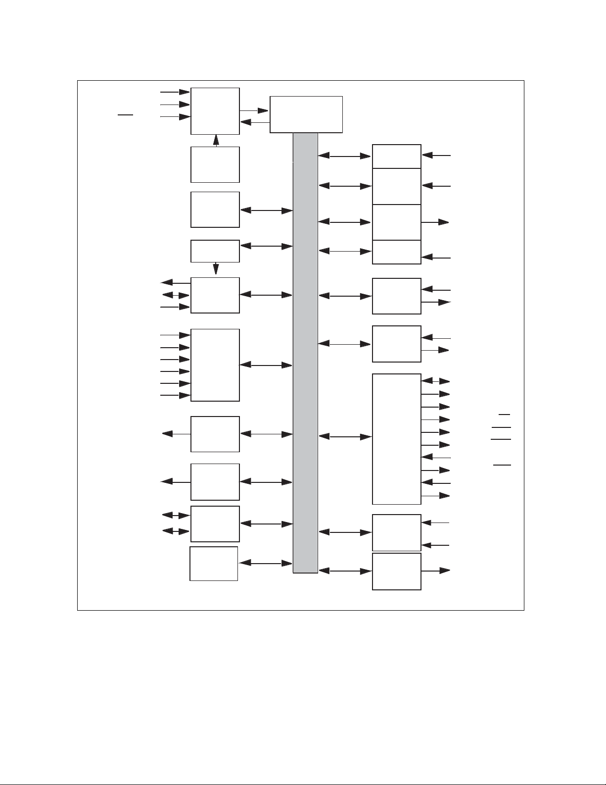
1.2 Block Diagram of MB90360 series
Figure 1.2-3 shows a block diagram of the MB90360.
■ Block Diagram of Evaluation Chip
Figure 1.2-1 Block Diagram of Evaluation Chip (MB90V340A-101/102)
CHAPTER 1 OVERVIEW
X0, X1
X0A, X1A *
RST
SOT4 to SOT0
SCK4 to SCK0
SIN4 to SIN0
AV
CC
AV
SS
AN23 to AN0
AVRH
AVRL
ADTG
DA01, DA00
PPGF to PPG0
Clock
control
RAM 30KB
Prescaler
(5 channels)
UART
(5 channels)
8-/10-bit
A/D
converter
24 channels
10-bit
D/A
converter
2 channels
8-/16-bit
PPG
16 channels
2
MC-16LX core
F
Internal data bus
16-bit
I/O timer 0
Input
capture
8 channels
Output
compare
8 channels
16-bit
I/O timer 1
CAN
controller
3 channels
16-bit
reload
timer
4 channels
External
bus
FRCK0
IN7 to IN0
OUT7 to OUT0
FRCK1
RX2 to RX0
TX2 to TX0
TIN3 to TIN0
TOT3 to TOT0
AD15 to AD00
A23 to A16
ALE
RD
WRL
WRH
HRQ
HAK
RDY
CLK
SDA1, SDA0
SCL1, SCL0
I2C
interface
2channels
DMA
*: Support MB90V340A-102 only
DTP/
external
interrupt
Clock
monitor
INT15 to INT8
(INT15R to INT8R)
INT7 to INT0
CKOT
9
Page 26
CHAPTER 1 OVERVIEW
Figure 1.2-2 Block Diagram of Evaluation Chip (MB90V340A-103/104)
X0,X1
X0A,X1A
RST
SOT4 to SOT0
SCK4 to SCK0
SIN4 to SIN0
AV
cc
AV
ss
AN23 to AN0
AVRH
AVRL
ADTG
DA01 , DA00
PPGF to PPG0
SDA1 , SDA0
SCL1 , SCL0
*
Clock
control
CR
oscillation
circuit
RAM 30KB
Prescaler
(5 channels)
UART
5 channels
8-/10-bit
A/D
converter
24 channels
F2MC-16LX core
16-bit
I/O timer 0
Input
capture
8 channels
Output
compare
8 channels
16-bit
I/O timer 1
CAN
controller
3 channels
16-bit
reload timer
4 channels
FRCK0
IN7 to IN0
OUT7 to OUT0
FRCK1
RX2 to RX0
TX2 to TX0
TIN3 to TIN0
TOT3 to TOT0
AD15 to AD00
Internal data bus
A23 to A16
ALE
10-bit D/A
converter
2 channels
External
bus
RD
WRL
WRH
HRQ
8-/16-bit
PPG
16 channels
2
I
C
Interface
2 channels
DTP/
external
interrupt
INT15 to INT8
(INT15R to INT8R)
INT7 to INT0
HAK
RDY
CLK
10
DMA
: Support MB90V340A-104 only
*
Clock
monitor
CKOT
Page 27
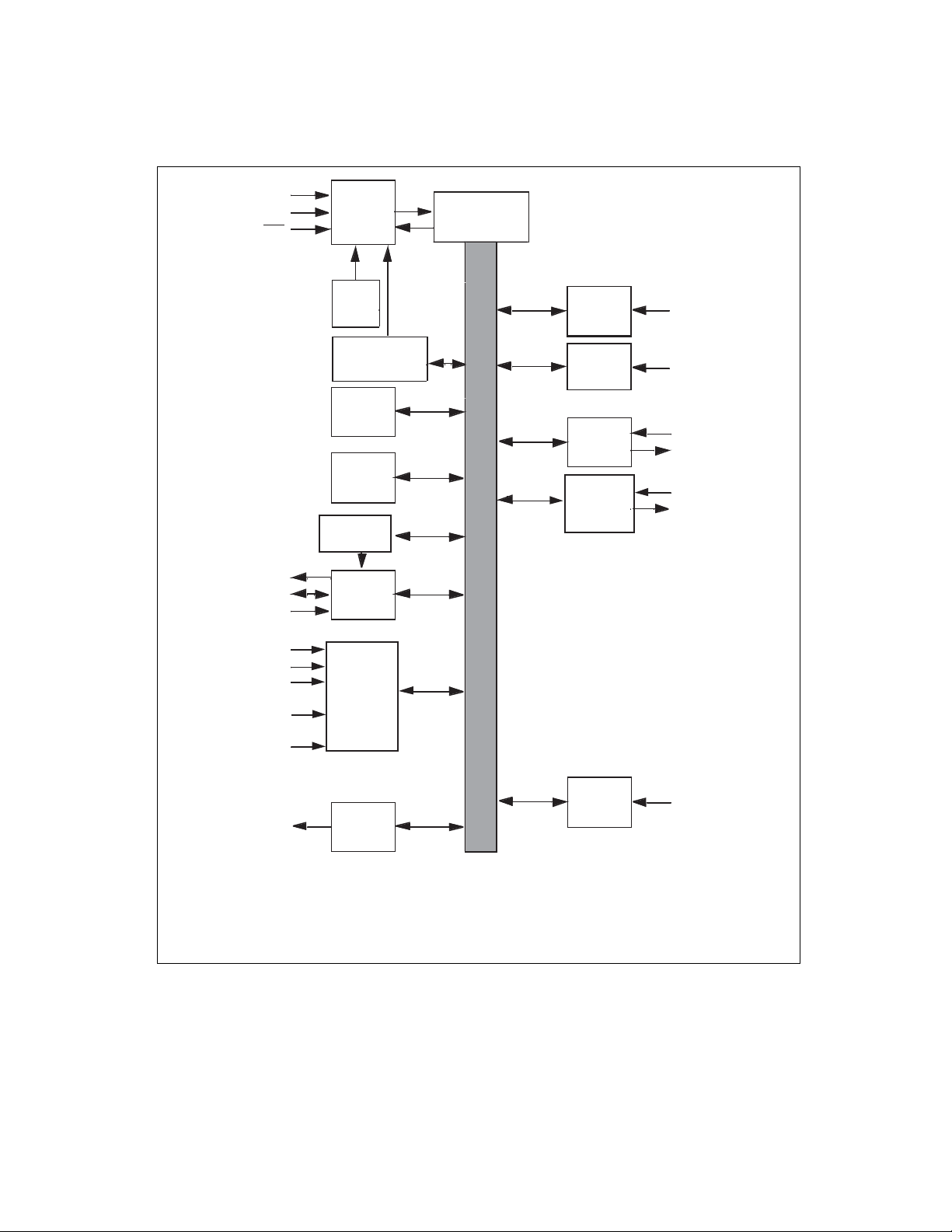
■ Block Diagram of Flash/Mask ROM Version
Figure 1.2-3 Block Diagram of Flash/Mask ROM Version
CHAPTER 1 OVERVIEW
X0A,X1A *
SOT0,SOT1
SCK0,SCK1
SIN0,SIN1
X0,X1
RST
1
Clock
control/
monitor *
CR
oscillation
circuit
Low voltage
detection*
CPU operation
detection*
RAM
3KB
ROM
64KB
Prescaler
(2 channels)
UART
2 channels
3
F2MC-16LX core
Input
capture
IN0 to IN3
4 channels
2
2
Internal data bus
16-bit
I/O
timer 0
CAN
controller
1 chnnal
16-bit
reload
timer
FRCK0
RX1
TX1
TIN2,TIN3
TOT2,TOT3
2 channels
AV
CC
AV
SS
AN15 to AN0
AVR
8/10-bit
A/D
converter
16 channels
ADTG
INT8,INT9R
INT10,INT11
INT12R,INT13
INT14R,INT15R
PPGF(E),PPGD(C),
PPGC(D),PPGE(F)
8/16bit
PPG
2 channels
DTP/
external
interrupt
*1: Product without S-suffix
*2: Product with T-suffix
*3: CR oscillation circuit/clock supervisor supports MB90367/T(S), MB90F367/T(S) only
11
Page 28
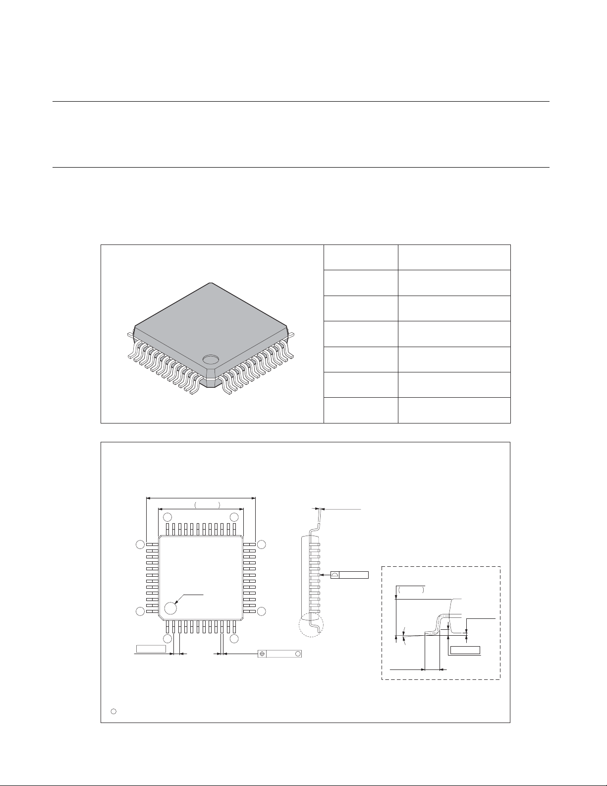
CHAPTER 1 OVERVIEW
1.3 Package Dimensions
MB90360 series has a package.
Note that the dimensions show below are reference dimensions. For formal dimensions
of each package, contact us.
■ Package Dimensions
Figure 1.3-1 shows the package dimensions of LQFP-48 type.
Figure 1.3-1 Package Dimensions of LQFP-48 Type
48-pin plastic LQFP Lead pitch 0.50 mm
(FPT-48P-M26)
48-pin plastic LQFP
(FPT
-48P-M26)
9.00±0.20(.354±.008)SQ
+0.40
*
.276
7.00
–0.10
36
37
+.016
–.004
Package width ×
package length
7 × 7 mm
Lead shape Gullwing
Sealing method Plastic mold
Mounting height 1.70 mm MAX
Weight 0.17 g
Code
(Reference)
Note 1)* : These dimensions include resin protrusion.
Note 2) Pins width and pins thickness include plating thickness.
Note 3) Pins width do not include tie bar cutting remainder.
SQ
25
24
0.145±0.055
(.006±.002)
P-LFQFP48-7×7-0.50
12
INDEX
48
1
LEAD No.
0.50(.020)
C
2003 FUJITSU LIMITED F48040S-c-2-2
12
0.20±0.05
(.008±.002)
13
0.08(.003)
0.08(.003)
"A"
M
Details of "A" part
+0.20
1.50
–0.10
(Mounting height)
+.008
.059
–.004
0.10±0.10
0˚~8˚
0.60±0.15
(.024±.006)
Dimensions in mm (inches).
Note: The values in parentheses are reference values.
(.004±.004)
0.25(.010)
(Stand off)
Page 29
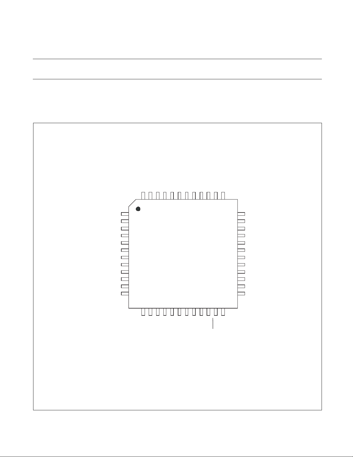
1.4 Pin Assignment
This section shows the pin assignments for the MB90360 series.
■ Pin assignment (LQFP-48)
Figure 1.4-1 shows the pin assignments of LQFP-48 type.
Figure 1.4-1 Pin Assignment (LQFP-48)
(TOP VIEW)
P84/SCK0/INT15R
P83/SOT0/TOT2
P42/RX1/INT9R
P43/TX1
P86/SOT1
P87/SCK1
AVss
X1A/P41 *1
X0A/P40 *1
P82/SIN0/INT14R/TIN2
P44/FRCK0
P85/SIN1
CHAPTER 1 OVERVIEW
AVcc
AVR
P60/AN0
P61/AN1
P62/AN2
P63/AN3
P64/AN4
P65/AN5
P66/AN6/PPGC(D)
P67/AN7/PPGE(F)
P80/ADTG/INT12R
P50/AN8
4847464544434241403938
1
2
3
4
5
6
7
8
9
10
11
12
1314151617181920212223
P51/AN9
P52/AN10
TOP VIEW
P53/AN11/TIN3
P55/AN13/INT10
P56/AN14/INT11
P57/AN15/INT13
P54/AN12/TOT3/INT8
(FPT-48P-M26)
MD2
MD1
MD0
RST
37
24
Vcc
36
35
34
33
32
31
30
29
28
27
26
25
P20
P21
P22/PPGD(C)
P23/PPGF(E)
P24/IN0
P25/IN1
P26/IN2
P27/IN3
X1
X0
C
Vss
*2
*2
*2
*2
*1: MB90F362/T, MB90362/T, MB90F367/T, MB90367/T : X0A, X1A
MB90F362S/TS, MB90362S/TS, MB90F367S/TS, MB90367S/TS : P40, P41
*2: High current port
13
Page 30
CHAPTER 1 OVERVIEW
1.5 Pin Functions
Table 1.5-1 describes the pin functions of the MB90360 series.
■ Pin Functions
Table 1.5-1 Pin Description (1/3)
Pin number Pin name Circuit type Functional description
1AV
CC
IV
power input pin for analog circuit
CC
2 AVR - Power (Vref+) input pin for A/D converter. The power supply
should not be input V
exceeding.
CC
3 to 8 P60 to P65 H General-purpose I/O port
AN0 to AN5 Analog input pin for A/D converter.
9 to 10 P66, P67 H General-purpose I/O port
AN6, AN7 Analog input pin for A/D converter
PPGC(D),
Output pin for PPG
PPGE(F)
11 P80 F General-purpose I/O port
ADTG Trigger input pin for A/D converter
INT12R External interrupt request input pin for INT12R.
12 to 14 P50 to P52 H General-purpose I/O port (I/O circuit type of P50 is different from
that of MB90V340A)
AN8 to AN10 Analog input pin for A/D converter
15 P53 H General-purpose I/O port
AN11 Analog input pin for A/D converter
TIN3 Event input pin for reload timer 3
16 P54 H General-purpose I/O port
AN12 Analog input pin for A/D converter
TOT3 Output pin for reload timer 3
INT8 External interrupt request input pin for INT8
17 to 19 P55 to P57 H General-purpose I/O port
AN13 to AN15 Analog input pin for A/D converter
INT10, INT11,
External interrupt request input pin for INT10, INT11 and INT13
INT13
20 MD2 D Input pin for selecting operation mode
21, 22 MD1,MD0 C Input pin for selecting operation mode
23 RST E Reset input
24 V
25 V
CC
SS
- Power input pin (3.5 V to 5.5 V)
- Power input pin (0 V)
14
Page 31

Table 1.5-1 Pin Description (2/3)
Pin number Pin name Circuit type Functional description
26 C I Capacity pin for stabilizing power supply.
It should be connected to higher than or equal to 0.1 µF ceramic
capacitor.
27 X0 A Oscillation input pin
28 X1 A Oscillation output pin
29 to 32 P24 to P27 G General-purpose I/O port
The register can be set to select whether to use pull-up register.
This function is enabled in single-chip mode.
IN0 to IN3 Event input pin for i nput captur e 0 to 3.
33, 34 P22 to P23 J General-purpose I/O port
The pull-up resistor ON/OFF can be set by setting the register.
This function becomes valid at shingle-chip mode.
High current output port
PPGF(E),
PPGD(C)
35, 36 P20, P21 J General-purpose I/O port
37 P85 K General-purpose I/O port
SIN1 Serial data input pin for UART1
38 P87 F General-purpose I/O port
SCK1 Clock I/O pin for UART1
39 P86 F General-purpose I/O port
SOT1 Serial data ou tput pin for UART1
40 P43 F General-purpose I/O port
TX1 TX output pin for CAN1 interface
41 P42 F General-purpose I/O port
RX1 RX input pin for CAN1 interface
INT9R External interrupt request input pin for INT9R (sub)
42 P83 F General-purpose I/O port
SOT0 Serial data ou tput pin for UART0
TOT2 Output pin for reload timer 2
43 P84 F General-purpose I/O port
SCK0 Clock I/O pin for UART0
INT15R External interrupt request input pin for INT15R
44 P82 K General-purpose I/O port
SIN0 Serial data input pin for UART0
INT14R External interrupt request input pin for INT14R
TIN2 Event input pin for reload timer 2
Output pin for PPG
The pull-up resistor ON/OFF can be set by setting the register.
This function becomes valid at shingle-chip mode.
High current output port
CHAPTER 1 OVERVIEW
15
Page 32

CHAPTER 1 OVERVIEW
Table 1.5-1 Pin Description (3/3)
Pin number Pin name Circuit type Functional description
45 P44 F General-purpose I/O port (I/O circuit t ype of P44 is different fr om
that of MB90V340A.)
FRCK0 Free-run timer 0 clock pin
46, 47 P40, P41 F General-purpose I/O port
(product with S-suffix and MB90V340A-101/103 only)
X1A, X0A B Oscillation input pin for subclock
(product without S-suffix and MB90V340A-102/104 only)
48 AV
SS
IV
power input pin for analog circuit
SS
16
Page 33

CHAPTER 1 OVERVIEW
1.6 Input-Output Circuits
Table 1.6-1 lists the input-output circuits.
■ Input-output Circuits
Table 1.6-1 I/O Circuit Types (1/4)
Type Circuit Remarks
A Oscillation circuit
X1
Xout
High-speed oscillation feedback resistor =
approx. 1 MΩ
X0
Standby control signal
B Oscillation circuit
X1A
Xout
Low-speed oscillation feedback resistor =
approx. 10 MΩ
X0A
Standby control signal
C Mask ROM device :
R
Hysteresis
input
CMOS hysteresis input pin
Flash device:
CMOS input
D Mask ROM device :
R
Pull-down
resistor
Hysteresis
input
CMOS hysteresis input pin
Pull-down resi stor value: approx. 50 kΩ
Flash device:
CMOS input pin
No Pull-down
17
Page 34

CHAPTER 1 OVERVIEW
Table 1.6-1 I/O Circuit Types (2/4)
Type Circuit Remarks
E CMOS hysteresis input pin
Pull-up resister value: approx. 50 kΩ
Pull-up
resistor
R
Hysteresis
input
F CMOS level output
(I
= 4 mA, IOH =-4 mA)
Pout
OL
CMOS hysteresis inputs
(with the standby-time input shutdown
Nout
R
Hysteresis input
Automotive input
Standby control for
input shutdown
function)
Automotive input
(with the standby-time input shutdown
function)
G CMOS level output
Pull-up control
(I
= 4 mA, IOH =-4 mA)
OL
CMOS hysteresis inputs
Pout
(with the standby-time input shutdown
function)
Automotive input
Nout
R
Hysteresis input
(with the standby-time input shutdown
function)
Programmable pull-up resistor: approx. 50 kΩ
18
Automotive input
Standby control for
input shutdown
Page 35

CHAPTER 1 OVERVIEW
t
ut
Table 1.6-1 I/O Circuit Types (3/4)
Type Circuit Remarks
H CMOS level output
(I
= 4 mA, IOH =-4 mA)
Pou
OL
CMOS hysteresis inputs
(with the sta ndby-time inpu t shutdown
No
function)
Automotive input
R
Hysteresis input
Automotive input
Standby control for
input shutdown
Analog input
(with the sta ndby-time inpu t shutdown
function)
A/D analog input
I Power supply input protection circuit
J CMOS level output
(I
Pull-up control
= 20 mA, IOH =-14 mA)
OL
CMOS hysteresis inputs
High current output
Pout
(with the sta ndby-time inpu t shutdown
function)
Automotive inputs
High current output
Nout
R
Hysteresis input
Automotive input
Standby control for
input shutdown
(with the sta ndby-time inpu t shutdown
function)
Programmable pull-up resistor: approx. 50 kΩ
19
Page 36

CHAPTER 1 OVERVIEW
r
Table 1.6-1 I/O Circuit Types (4/4)
Type Circuit Remarks
K CMOS level output
(I
= 4 mA, IOH = -4 mA)
OL
Pout
CMOS hysteresis inputs
(with the standby-time input shutdown
function)
Nout
R
CMOS input
Automotive input
Standby control fo
input shutdown
Automotive hysteresis inputs
(with the standby-time input shutdown
function)
20
Page 37

1.7 Handling Device
This section explains notes on handling the MB90360 series.
■ Handling the Device
Preventing latch-up
●
CMOS IC chips may suffer latch-up under the following conditions:
• A voltage higher than V
• A voltage higher than the rated voltage is applied between V
•The AV
Latch-up may increase the power supply current drastically, causing thermal damage to the device.
When used, note that maximum rated voltage is not exceeded.
For the same reason, also be careful not to let the analog power-supply voltage (AV
digital power-supply volt age.
power supply is applied before the VCC voltage.
CC
or lower than VSS is applied to an input or output pin.
CC
and VSS.
CC
CHAPTER 1 OVERVIEW
AVR) exceed the
CC,
Treatment of unused pins
●
Leaving unused input pins open may result in misbehavior or latch up and possible permanent damage of
the device. Therefore, they must be pulled up or pulled down through resistors. In this case those resistors
should be more than 2 kΩ.
Unused bidirectional pins should be set to the output state and can be left open, or the input state with the
above described connection.
21
Page 38

CHAPTER 1 OVERVIEW
Using external clock
●
To use external clock, drive the X0 (X0A) pin and leave X1 (X1A) pin open.
Figure 1.7-1 Using External Clock
MB90360 series
X0 (X0A)
Open
Precautions for when not using a sub clock signal
●
If you do not connect pins X0A and X1A to an os cillator, use pull-down handling on the X0A pin, and
leave the X1A pin open.
Notes on during operation of PLL clock mode
●
If the PLL clock mode is selected, the microcontroller attempts to be working with the free-running
frequency of self-oscillating circuit in the PLL even when there is no external oscillator or external clock
input is stopped. Performance of this operation, however, cannot be guaranteed.
Power supply pins (VCC/VSS)
●
• If there are multiple V
and VSS pins, from the point of view of device design, pins to be of the same
CC
potential are connected the inside of the device to prevent such malfunctioning as latch up.
To reduce unnecessary radiation, prevent malfunctioning of the strobe signal due to the rise of ground
level, and to keep the recommended DC characteristics specified as the total output current, be sure to
connect the V
• Connect V
and VSS pins to the power supply and ground externally (see Figure 1.7-2 ).
CC
and VSS to the device from the power supply source with lowest possible impedance.
CC
• It is recommended to connect a capacitor of about 0.1 µF as a bypass capacitor between V
the vicinity of V
and VSS pins of the device
CC
X1 (X1A)
and VSS in
CC
22
Page 39

CHAPTER 1 OVERVIEW
Pull-up/down resistors
●
The MB90360 Series does not support internal pull-up/down resistors (except Port2:
programmable pull-up resistors). Use pull-up/down handling where needed.
Figure 1.7-2 Power Supply Pins (V
Vss
Vcc
Vss
Vcc
MB90360
series
Vss
Vcc
Vss
Vcc
CC/VSS
Vcc
Vss
)
Crystal Oscillator Circuit
●
Noises aroun d X 0 or X 1 pin s ma y be p oss ibl e cau ses of abno rm al op era tions . M ake s ure to pro vide byp ass
capacitors via shortest distance from X0, X1 pins, crystal oscillator (or ceramic resonator) and ground lines,
and make sure, to the utmost effort, that lines of oscillation circuit not cross the lines of other circuits.
It is highly recommended to provide a printed circuit board art work surrounding X0 and X1 pins with a
ground area for stabilizing the operation.
Turning-on Sequence of Power Supply to A/D Converter and Analog Inputs
●
Make sure to turn on the A/D converter power supply (AV
after turning-on the digital power supply (V
CC
).
, AVR) and analog inputs (AN0 to AN15)
CC
Turn-off the digital power supply after turning off the A/D converter power supply and analog inputs. In
this case, make sure that the voltage not exceed AVR or AV
Connection of Unused Pins of A/D Converter
●
Connect unused pins of A/D converter as AV
= VCC, AVSS = AVR = VSS.
CC
CC
.
23
Page 40

CHAPTER 1 OVERVIEW
Notes on Energization
●
To prevent malfunction of the internal voltage regulator, supply voltage profile while turning on the power
supply should be slower than 50 µs from 0.2 V to 2.7 V.
Stabilization of power supply voltage
●
If the power supply voltage varies acutely even within the operation assurance range of the V
supply voltage, a malfunction may occur. The V
stabilization guidelines, stabilize the power supply voltage so that V
power supply voltage must therefore be stabilized. As
CC
ripple fluctuations (peak to peak
CC
value) in the commercial frequencies (50 to 60 Hz) fall within 10% of the standard V
voltage and the transient fluctuation rate becomes 0.1 V/m s or less in instantaneous fluctuation for power
supply switching .
Note on using CAN Function
●
The MB90360 series does not contain the clock modulation function. So, at using CAN, the DIRECT bit of
the CAN direct mode register (CDMR) must be set "1". (See Table 1.7-1 ). If the DIRECT bit is not set
correctly, the device does not operate normally.
Table 1.7-1 Setting of Clock Modulation and CAN Direct Mode
Clock modulation setting
(CMCR:PMOD bit)
Required setting 0: Disable clock modulation
1: Enable CAN direct mode
CAN direct mode setting
(setting of CDMR:DIRECT bit)
(initial value)
Setting disabled 1: Enable clock modulation 0: Disable CAN direct mode
(initial value)
CC
power supply
CC
power
24
Note:
For details on the clock modulation, see "CHAPTER 6 CLOCK SUPERVISOR".
For details on the CAN direct mode, see "21.11 Setting Configuration of Multi-level Message Buffer".
Page 41

Flash security Function
●
The security bit is located in the area of the flash memory.
If protection code 0 1
security.
Therefore please do not write 01
Please refer to following table for the address of the security bit.
CHAPTER 1 OVERVIEW
is written in the security bit, th e flash memor y is in the protected state by
H
in this address if you do not use the security function.
H
Flash memory size Address of security bit
MB90F362/T(S),
MB90F367/T(S)
For the diversion of MB90340-series software assets
●
Embedded 512Kbit flash memory FF0001
H
In programming of the MB90360 series, keep the following points in mind for the diversion of
MB90340-series software assets in particular.
• Access to the registers which do not exist in the MB90360 series.
As for the registe rs and bits wh ich exist i n MB90340 s eries but not in the MB903 60 series, d o
not access them or ensur e that the initial value is set. Setting any other value than the initial
value may cause an abnormal operation in emulation using MB90V340.
• Setting of the external interrupt factor select register (EISSR).
The MB90360 series i s not equipped with the external interrupt requ est input, INT8R, INT9,
INT10, INT11, INT12, INT13, INT14 and INT15.
Enabling unequipped terminals causes a false operation. First set the EISSR and then set
each of the registers when DTP/external interrupt is us ed.
25
Page 42

CHAPTER 1 OVERVIEW
26
Page 43

CHAPTER 2
This chapter explains the CPU.
2.1 Outline of the CPU
2.2 Memory Space
2.3 Memory Map
2.4 Linear Addressing
2.5 Bank Addressing Types
CPU
2.6 Multi-byte Data in Memory Space
2.7 Registers
2.8 Register Bank
2.9 Prefix Codes
2.10 Interrupt Disable Instructions
2.11 Precautions for Use of "DIV A, Ri" and "DIVW A, RWi" Instructions
27
Page 44

CHAPTER 2 CPU
2.1 Outline of the CPU
The F2MC-16LX CPU core is a 16-bit CPU designed for applications that require highspeed real-time proces sing, such as home-use or vehicle-mounted electronic
appliances. The F2MC-16LX instruction set is designed for controller applications, and
is capable of high-speed, highly efficient control processing.
■ Outline of the CPU
In addition to 16-bit data, the F2MC-16LX CPU core can process 32-bit data by using an internal 32-bit
accumulator. (32-bit data can be processed with some instructions.) Up to 16M bytes of memory space
(expandable) can be used, which can be accessed by either the linear pointer or bank method. The
instruction system, based on the F
compatible with high-level languages, expandi ng address ing mod es, reinforci ng multip lication and divisio n
instructions, and enhancing bit processing. The features of the F
2
MC-8 A-T architecture, has been reinforced by adding instructions
2
MC-16LX CPU are explained below.
Minimum instruction execution time: 42 ns (at 4-MHz oscillation, 6 times clock multiplication)
●
Maximum memory space: 16M bytes, accessed in linear or bank mode
●
Instruction set optimized for controller applications
●
• Rich data types: Bit, byte, word, long word
• Extended addressing modes: 23 types
• High-precision operation (32-bit length) based on 32-bit accumulator
Powerful interrupt functions
●
Eight priority levels (programmable)
CPU-independent automatic transfer
●
Up to 16 channels of the extended intelligent I/O service
Instruction set compatible with high-level language (C)/multitasking
●
System stack pointer/instruction set symmetry/barrel-shift instructions
Improved execution speed: 4 bytes queue
●
28
Page 45

CHAPTER 2 CPU
2.2 Memory Space
An F2MC-16LX CPU has a 16M bytes memory space. All data program input and output
managed by the F2MC-16LX CPU are located in this 16M bytes memory space. The CPU
accesses the resources by indicating their addresses using a 24-bit address bus.
■ Outline of CPU Memory Space
Figure 2.2-1 shows a sample relationship between the F2MC-16LX system and memory map.
2
Figure 2.2-1 Sample Relationship between F
MC-16LX System and Memory Map
F2MC-16LX device
Programs
Peripheral circuit
2
F
MC-16LX
CPU
Data
EI
2
OS
Internal data bus
Peripheral circuit
Interrupt
Peripheral circuit
General-purpose
ports
*1: The size of the internal ROM differs for each model.
*2: The size of the internal RAM differs for each model.
*3: Access is not possible in single-chip mode.
FFFFFF
FFFC00
FF0000
100000
010000
008000
007900
001900
000380
000180
000100
0000F0
0000C0
0000B0
000020
000000
H
Vector table area
H
*1
H
H
H
H
H
*2
H
H
H
H
H
H
H
H
H
Program area
External area
ROM area
(FF bank image)
Peripheral function
control register area
Data area
General-purpose register
EI2OS
descriptor area
External area
Peripheral function control
register area
Interrupt control
register area
Peripheral function control
register area
I/O port control
register area
ROM area
*3
I/O area
RAM area
*3
I/O area
29
Page 46

CHAPTER 2 CPU
■ ROM area
Vector table area (address: FFFC00H to FFFFFFH)
●
This area is used as a vector table for reset/interrupt and CALLV vector.
This area is allocated at the highest addresses of the ROM area. The start address of the corresponding
processing routine is set as data in each vector table address.
Program area (address: FF0000H to FFFBFFH)
●
ROM is built in as an internal program area.
The size of internal ROM differs for each model.
■ RAM Area
Data area (address: From 000100H to 000CFFH (for 3K bytes))
●
The static RAM is built in as an internal data area.
The size of internal RAM differs for each model.
General-purpose register area (address: 000180H to 00037FH)
●
Extended intelligent I/O service (EI2OS) descriptor area (address: 000100H to 00017FH)
●
■ I/O Area
Interrupt control register area (address: 0000B0H to 0000BFH)
●
Peripheral function control register area (address: 000020H to 0000AF
●
007900H to 007FFFH)
Auxiliary registers used for 8-bit, 16-bit, and 32-bit arithmetic operations and transfer are allocated in this
area.
Since this area is allocated to a part of the RAM area, it can be used as ordinary RAM.
When this area is used as a general-purpose register, general-purpose register addressing enables high-
speed access with short instructions.
This area retains the transfer modes, I/O addresses, transfer count, and buffer addresses.
Since this area is allocated to a part of the RAM area, it can be used as ordinary RAM.
The interrupt control registers (ICR00 to ICR15) correspond to all peripheral functions that have an
interrupt function. These registers set interrupt levels and control the extended intelligent I/O service
2
OS).
(EI
0000C0H to 0000EF
H ,
H ,
30
This register controls the built-in peripheral functions and inputs and outputs data.
I/O port contr ol re giste r ar ea (addr es s: 000000H to 00001FH)
●
This register controls I/O ports, and inputs and outputs data.
Page 47

■ Address generation types
The F2MC-16LX has the following 2 addressing modes:
Linear addressing
●
An entire 24-bit address is specified by an instruction.
Bank addressing.
●
The eight high-order bits of an address are specified by an appropriate bank register, and the remaining 16
low-order bits are specified by an instruction.
CHAPTER 2 CPU
31
Page 48

CHAPTER 2 CPU
2.3 Memory Map
The memory map of the MB90360 Series is shown in Figure 2.3-1 .
■ Memory Map
The ROM data in the high-order portion of FF-bank can be seen as an image in the higher 00-bank in order
to support the small model C compiler. Sin ce the low-order 16 b its are iden tical, this part of the ROM dat a
can be referred without using the far specification in the pointer declaration.
For example, when 00C000
ROM area in the FF bank exceeds 32K bytes, its entire image cannot be mirrored in the 00 bank.
is accessed, the contents of ROM at FFC000H are read. However, since the
H
The image between FF8000
FF7FFF
is only visible in bank FF.
H
MB90V340A-101/102/103/104
FFFFFFH
FF0000H
FEFFFFH
FE0000H
FDFFFFH
FD0000H
FCFFFFH
FC0000H
FBFFFFH
FB0000H
FAFFFFH
FA0000H
F9FFFFH
F90000H
F8FFFFH
F80000H
00FFFFH
008000H
007FFFH
007900H
0078FFH
ROM (FF bank)
ROM (FE bank)
ROM (FD bank)
ROM (FC bank)
ROM (FB bank)
ROM (FA bank)
ROM (F9 bank)
ROM (F8 bank)
(image of FF bank)
Peripheral
and FFFFFFH is visible in bank 00, whereas the data between FF0000H and
H
Figure 2.3-1 Memory Map
MB90F362/T(S)
MB90362/T(S)
MB90F367/T(S)
MB90367/T(S)
ROM
FFFFFFH
FF0000H
FEFFFFH
010000H
00FFFFH
008000H
007FFFH
007900H
ROM (FF bank)
ROM
(image of FF bank)
Peripheral
32
000100H
0000EFH
000000H
RAM 30KB
Peripheral
Access prohibited
000CFFH
000100H
0000FFH
0000F0H
0000EFH
000000H
RAM 3KB
Peripheral
Page 49

CHAPTER 2 CPU
2.4 Linear Addressing
There are 2 types of linear addressing:
• 24-bit operand specification: Directly specifies a 24-bit address using operands.
• 32-bit register indirect specification: Indirectly specifies the 24 low-order bits of a 32bit general-purpose register value as the address.
■ 24-bit Operand Specification
Figure 2.4-1 shows an example of 24-bit operand specification. Figure 2.4-2 shows an example of 32-bit
register indirect specification.
Figure 2.4-1 Example of Linear Method (24-bit operand specification)
JMPP 123456H
Old program counter
+ Program bank
New program counter
+ Program bank
12
17
452D
3456
17452DH
123456H
JMPP 123456H
Next instruction
Figure 2.4-2 Example of Linear Method (32-bit register indirect specification)
MOV A, @RL1+7
090700
Old AL
XXXX
7
(The high-o rder 8 bits ar e ignor ed.)
H
RL1
3A
240906F9
New AL
003A
33
Page 50

CHAPTER 2 CPU
2.5 Bank Addressing Types
In the bank method, the 16M bytes space is divided into 256 for 64K bytes banks. The
following 5 bank registers are used to specify the banks corresponding to each space:
• P rogram bank register (PCB)
• Data bank regist er (DTB)
• User stack bank register (USB)
• System stack bank register (SSB)
• Additional bank register (ADB)
■ Bank Addressing Types
Program bank register (PCB)
●
The 64K bytes bank specified by the PCB is called a program (PC) space. The PC space contains
instruction codes, vector tables, and immediate value data, for example.
Data bank register (DTB)
●
The 64K bytes bank specified by the DTB is called a data (DT) space. The DT space contains readable/
writable data, and control/data registers for internal and external resources.
User stack bank register (USB)/system stack bank register (SSB)
●
The 64K bytes bank specified by the USB or SSB is called a stack (SP) space. The SP space is accessed
when a stack access occurs during a push/pop instruction or interrupt register saving. The S flag in the
condition code register determines the stack space to be accessed.
Additional bank register (ADB)
●
The 64K bytes bank specified by the A DB is called an additional (AD) s pace. The AD space, for example,
contains data that cannot fit into the DT space.
Table 2.5-1 lists the default spaces used in each addressing mode, which are pre-determined to improve
instruction coding efficiency. To use a non-default space for an addressing mode, specify a prefix code
corresponding to a bank before the instruction. This enables access to the bank space corresponding to the
specified prefix code.
After reset, the DTB, USB, SSB, and ADB are initialized to 00
by the reset vector. After reset, the DT, SP, and AD spaces are allocated in bank 00
00FFFF
), and the PC space is allocated in the bank specified by the reset vector.
H
. The PCB is initialized to a value specified
H
(000000H to
H
34
Page 51

Table 2.5-1 Default Space
Default space Addressing mode
Program space PC indirect, program access, branch
Data space Addressing mode using @RW0, @RW1, @RW4, or @RW5, @A, addr16, and dir
Stack space Addressing mode using PUSHW, POPW, @RW3, or @RW7
Additional space Addressing mode using @RW2 or @RW6
Figure 2.5-1 is an example of a memory space divided into register banks.
Figure 2.5-1 Physical Addresses of Each Space
CHAPTER 2 CPU
Physical address
FFFFFFH
FF0000H
B3FFFFH
B30000H
92FFFFH
920000H
68FFFFH
680000H
4BFFFFH
4B0000H
000000H
Program space
Additional space
User stack space
Data space
System stack space
FFH
B3H
92H
68H
4BH
: PCB (Program bank register)
: ADB (Additional bank register)
: USB (User stack bank register)
: DTB (Data bank register)
: SSB (System stack bank register)
35
Page 52

CHAPTER 2 CPU
2.6 Multi-byte Data in Memory Space
Data is written to memory from the low-order addresses. Therefore, for a 32-bit data
item, the low-order 16 bits are transferred before the high-order 16 bits.
If a reset signal is inputted immediately after the low-order bits are written, the highorder bits might not be written.
■ Multi-byte Data Allocation in Memory Space
Figure 2.6-1 is a diagram of multi-byte data configuration in memory. The low- order eight bits of a data
item are stored at address n, then address n+1, address n+2, address n+3, etc.
Figure 2.6-1 Sample Allocation of Multi-byte Data in Memory
H
01010101
MSB LSB
01010101
11001100 11111111 00010100
11001100
11111111
Address n
00010100
L
■ Accessing Multi-byte Data
Fundamentally, accesses are made within a bank. For an instruction accessing a multi-byte data item,
address FFFF
accessing multi-byte data.
80FFFF
800000H
is followed by address 0000H of the same bank. Figure 2.6-2 is an example of an instruction
H
Figure 2.6-2 Execution of MOVW A, 080FFFF
H
H
01H
23H
H
AL before execution
·
·
·
AL after execution
?? ??
H
23
01H
36
L
Page 53

CHAPTER 2 CPU
2.7 Registers
The F2MC-16LX regist ers are largely classified into two types: special regist ers in the
CPU and general-purpose registers in memory. The special registers are dedicated
internal hardware of the CPU, and they ha v e spec if ic use defined by the CPU
architecture. The general-purpose registers share the CPU address space with RAM.
The general-purpose registers are the same as the special registers in that they can be
accessed without using an address. The applications of the general-purpose registers
can be specified by the user however, as is ordinary memory space.
■ Special Registers
The F2MC-16LX CPU core has the following special registers:
• Accumulator (A=AH:AL) : Two 16-bit accumulators (Can be used as a single 32-bit accumulator.)
• User stack pointer (USP) : 16-bit pointer indicating the user stack area
• System stack pointer (SSP) : 16-bit pointer indicating the system stack area
• Processor status (PS) : 16-bit register indicating the system status
• Program counter (PC) : 16-bit register holding the address of the program
• Program bank register (PCB) : 8-bit register indicating the PC space
• Data bank register (DTB) : 8-bit register indicating the DT space
• User stack bank register (USB) : 8-bit register indicating the user stack space
• System stack bank register (SSB): 8-bit register indicating the system stack space
• Additional bank register (ADB) : 8-bit register indicating the AD space
• Direct page register (DPR) : 8-bit register indicating a direct page
Figure 2.7-1 is a diagram of the special registers.
37
Page 54

CHAPTER 2 CPU
Figure 2.7-1 Special Registers
AH AL
USP
SSP
PS
PC
DPR
PCB
DTB
USB
SSB
ADB
8 bits
Accumulator
User stack pointer
System stack pointer
Processor status
Program counter
Direct page register
Program bank register
Data bank register
User bank register
System stack bank register
Additional data bank register
32 bits
16 bits
38
Page 55

■ General-purpose registers
The F2MC-16LX general-purpose registers are located from addresses 000180H to 00037FH (maximum
configuration) of main storage. The register bank pointer (RP) indicates which of the above addresses are
currently being used as a register bank. Each bank has the following three types of registers. These registers
are mutually depend ent as desc ribed in Figure 2.7-2 .
• R 0 to R7: 8-bit general-purpose register
• RW0 to RW7: 16-bit genera l-purpose re gister
• RL0 to RL3: 32-bit general-purpose register
Figure 2.7-2 General-purpose Registers
CHAPTER 2 CPU
MSB LSB
16 bits
000180H RP x 10H
Start address of
general-purpose register
Low-order
High-order
R1
R3
R5
R7
RW0
RW1
RW2
RW3
R0
R2
R4
R6
RW4
RW5
RW6
RW7
RL0
RL1
RL2
RL3
The relationship between the high-order and low-order bytes of a byte or word register is expressed as
follows:
RW
(i+4)
= R
(i × 2+1)
× 256+R
(i × 2)
[i=0 to 3]
The relationship between the high-order and low-order bytes of RLi and RW can be expressed as follows:
RL
= RW
(i)
(i × 2+1)
× 65536+RW
(i × 2)
[i=0 to 3]
39
Page 56

CHAPTER 2 CPU
2.7.1 Accumulator (A)
The accumulator (A) register consists of 2 16-bit arithmetic operation registers (AH and
AL), and is used as a temporary storage for operation results and transfer data.
■ Accumulator (A)
During 32-bit data processing, AH and AL are used together. Only AL is used for word processing in 16bit data processing mode or for byte processing in 8-bit data processing mode (see Figure 2.7-3 and Figure
2.7-4 ). The data stored in the A register can be operated upon with the data in memory or registers (Ri,
Rwi, or RLi). In the same manner as with the F
AL, the previous data item in AL is automatically sent to AH (data preservation function). The data
preservation function and operation between AL and AH help improve processing efficiency.
When a byte or shorter data item is transferred to AL, the data is sign-extended or zero-extended and stored
as a 16-bit data item in AL. The data in AL can be handled either as word or byte long.
When a byte-processing arithmetic operation instruction is executed on AL, the high-order eight bits of AL
before operation are ignored. The high-order eight bits of the operation result all become zeroes.
The A register is not initialized by a reset. The A register holds an undefined value immediately after a
reset.
2
MC-8L, when a word or shorter data item is transferred to
A before
execution
A after
execution
A before
execution
A after
execution
MOVL A,@RW1+6
XXXXH XXXXH
8F74H 2B52H
AH AL
MOVW A,@RW1+6
XXXXH
DTB
1234H 1234H
Figure 2.7-3 32-bit Data Transfer
H
A61540
DTB
A6
H
+
A6153EH
6
RW1
Figure 2.7-4 AL-AH Transfer
A61540
1234H
A6
H
+6
H
A6153EH
RW1
MSB LSB
74H
52H
38H
74H
52H
38H
MSB
8F
2BH
15H
8FH
2BH
15H
H
LSB
40
Page 57

CHAPTER 2 CPU
2.7.2 User Stack Pointer (USP) and System Stack Pointer (SSP)
USP and SSP are 16-bit registers that indicate the memory addresses for saving and
restoring data when a push/pop instruction or subroutine is executed.
■ User Stack Pointer (USP) and System Stack Pointer (SSP)
The USP and SSP registers are used by stack instructions. The USP register is enabled when the S flag in
the processor status register is “0”, and the SSP register is enabled when the S flag is “1” (see
Figure 2.7-5 ). Since the S flag is set when an interrupt is accepted, register values are always saved in the
memory area indicated by SSP during interrupt processing. SSP is used for stack processing in an interrupt
routine, while USP is used for stack processing outside an interrupt routine. If the stack space is not
divided, use only the SSP.
During stack processing, the high-order eight bits of an address are indicated by SSB (for SSP) or USB (for
USP). USP and SSP are not initialized by a reset. Instead, they hold undefined values.
Figure 2.7-5 Stack Manipulation Instruction and Stack Pointer
Example of PUSHW A when S flag is "0"
Before execution
After execution
Example of PUSHW A when S flag is "1"
AL A624
S flag
AL A624
AL A624
AL A624
H
H
H
1
H
USB USP
USB USP
USB USP
USB USP
C6
56
C6
56
C6
56
C6
56
H
H
SSPSSB0
H
H
SSPSSB0
H
H
SSPSSB
H
H
SSPSSB1
F328
1234
F326
1234
F328
1234
F328
1232
MSB LSB
H
C6F326
H
H
System stack is used because S
H
H
H
H
H
H
flag is "0".
C6F326
H
561232
H
561232
H
System stack is used because
S flag is "1".
XX
A6
XX
A6
XX
H
24
H
XX
H
24
H
Note:
Specify an even-numbered address in the stack pointer whenever possible.
41
Page 58

CHAPTER 2 CPU
2.7.3 Processor Status (PS)
The PS register consists of the bits controlling the CPU operation and the bits
indicating the CPU status.
■ Processor Status (PS)
As shown in Figure 2.7-6 , the high-order byte of the PS register consists of a register bank pointer (RP)
and an interrupt level mask register (ILM). The ILM indicates the start address of a register bank. The loworder byte of the PS register is a condition code register (CCR), containing the flags to be set or reset
depending on the results of instruction execution or interrupt occurrences.
Figure 2.7-6 Processor Status (PS) Structure
15 13 12 8 7 0
PS ILM RP CCR
■ Condition Code Register (CCR)
Figure 2.7-7 is a diagram of condition code register (CCR) configuration.
Figure 2.7-7 Condition Code Register (CCR) Configuration
76543210
- ISTNZVC : CCR
Initial value - 0 1****** : Undefined
I: Interrupt enable flag:
●
Interrupt requests other than software interrupts are enabled when the I flag is 1 and are masked when the I
flag is 0. The I flag is cleared by a reset.
S: Stack flag:
●
When the S flag is 0, USP is enabled as the stack manipulation pointer.
When the S flag is 1, SSP is enabled as the stack manipulation pointer.
The S flag is set by an interrupt reception or a reset.
42
Page 59

T: Sticky bit flag:
●
1 is set in the T flag when there is at least one "1" in the data shifted out from the carry after execution of a
logical right/arithmetic right shift in struction. Otherwise, 0 is set in the T f lag. In addition, "0" is set in the
T flag when the shift amount is zero.
N: Negative flag:
●
The N flag is set when the MSB of the operation result is "1", and is otherwise cleared.
Z: Zero flag:
●
The Z flag is set when the operation result is all zeroes, and is otherwise cleared.
V: Overflow flag:
●
The V flag is set when an overflow of a signed value occurs as a result of operation execution and is
otherwise cleared.
C: Carry flag:
●
CHAPTER 2 CPU
The C flag is set when a carry-up or carry-down from the MSB occurs as a result of operation execution,
and is otherwise cleared.
■ Register Bank Pointer (RP)
The RP register indicates the relationship between the general-purpose registers of the F2MC-16LX an d th e
internal RAM addresses. Specifically, the RP register indicates the first memory address of the currently
used register bank in the following conversion expression: [00180
RP register consists of five bits, and can take a value between 00
at addresses from 000180
Even within that range, however, the register banks cannot be used as general-purpose registers if the banks
are not in internal RAM. The RP register is initialized to all zer oes by a reset. An instruction may t ransfer
an eight-bit immediate value to the RP register; however, only the low-order five bits of that data are used.
Figure 2.7-8 Register Bank Pointer (RP)
Initial value 0 0 0 0 0
+ (RP)*10H] (see Figure 2.7-8 ). The
H
and 1FH. Register banks can be allocated
H
to 00037H in memory.
H
B4 B3 B2 B1 B0 : RP
43
Page 60

CHAPTER 2 CPU
■ Interrupt level mask register (ILM)
The ILM register consists of thr ee bits, indicating th e CPU interrupt m asking level. An i nterrupt request is
accepted only when the level of the interrupt is higher than that indicated by these three bits. Level 0 is the
highest priority interrupt, and level 7 is th e lowest priority interrupt (see Table 2.7-1 ). Therefore, for an
interrupt to be accepted, its level value must be smaller than the current ILM value. When an interrupt is
accepted, the level value of that interrupt is set in ILM. Thus, an interrupt of the same or lower level cannot
be accepted subsequently. ILM is initialized to all zeroes by a reset. An instruction may transfer an eight-bit
immediate value to the ILM register, but only the low-order three bits of that data are used.
Figure 2.7-9 Interrupt Level Mask Register (ILM)
ILM2 ILM1 ILM0 : ILM
Initial value 0 0 0
Table 2.7-1 Levels Indicated by the Interrupt Level Mask (ILM) Register
ILM2 ILM1 ILM0 Level value Acceptable interrupt level
0 0 0 0 Interrupt disabled
001 1 0 only
0 1 0 2 Level value smaller than 1
0 1 1 3 Level value smaller than 2
1 0 0 4 Level value smaller than 3
1 0 1 5 Level value smaller than 4
1 1 0 6 Level value smaller than 5
1 1 1 7 Level value smaller than 6
44
Page 61

CHAPTER 2 CPU
2.7.4 Program Counter (PC)
The PC register is a 16-bit counter that indicates the low-order 16 bits of the memory
address of an instruction code to be executed by the CPU. The high-order eight bits of
the address are indicated by the PCB. The PC register is updated by a conditional
branch instruction, subroutine call instruction, interrupt, or reset.
The PC register can also be used as a base pointer for operand acc ess.
■ Program Counter (PC)
Figure 2.7-10 shows the program counter.
Figure 2.7-10 Program Counter
PCB
H ABCDH
FE
PC
Next instruction to be executed
FEABCDH
45
Page 62

CHAPTER 2 CPU
2.8 Register Bank
A register bank consists of eight words. The register bank can be used as the following
general-purpose registers for arithmetic operations: byte registers R0 to R7, word
registers RW0 to RW7, and long word registers RL0 to RL3. In addition, the register
bank can be used as instruction pointers.
RL0 to RL3 are used as the linear pointer that directly accesses entire space.
■ Register Bank
Table 2.8-1 lists the functions of the registers. Table 2.8-2 indicates the relationship between the registers.
In the same manner as for an ordinary RAM area, the register bank values are not initialized by a reset. The
status before a reset is maintained. When the power is tur ned on, however, the register bank will have an
undefined value.
Table 2.8-1 Register Functions
R0 to R7
RW0 to RW7
RL0 to RL3
T a ble 2.8-2 Relationship between Registers
R0
R1
R2
R3
R4
R5
R6
R7
Used as operands of instructions.
Note: R0 is used as a counter for barrel shift and normalization instructio ns .
Used as pointers.
Used as operands of instructions.
Note: RW0 is used as a counter for string instructions.
Used as long pointers.
Used as operands of instructions.
RW0
RW1
RW2
RW3
RW4
RW5
RW6
RW7
RL0
RL1
RL2
RL3
46
Direct page register (DPR) <Initial value: 01H>
●
DPR specifies addr8 to addr15 of the instruction operands in direct addressing mode as shown in Figure
Page 63

CHAPTER 2 CPU
2.8-1 . DPR is eight bits long, and is initialized to 01
by a reset. DPR can be read or written to by an
H
instruction.
Figure 2.8-1 Generating a Physical Address in Direct Addressing Mode
DTB register
DPR register
α α α α α α α α β β β β β β β β γ γ γ γ γ γ γ γ
MSB LSB
24-bit physical address
Program counter bank register (PCB) <Initial value: Value in reset vector>
●
Data bank register (DTB) <Initial value: 00H>
●
α α α α α α α α β β β β β β β β γ γ γ γ γ γ γ γ
Direct address during instruction
User stack bank register (USB) <Initial value: 00H>
●
System stack bank register (SSB) <Initial value: 00H>
●
Additional data bank register (ADB) <Initial value: 00H>
●
Each bank register indicates the memory bank where the PC, DT, SP (user), SP (system), or AD space is
allocated. All bank registers are one byte long. PCB is initialized to 00
than PCB can be read or written to. PCB can be read but cannot be written to.
PCB is updated when the JMPP, CALLP, RETP, RETIQ, or RETF instruction branching to the entire 16M
bytes space is executed or when an interrupt occurs. For operation of each register, see "2.2 Memory
Space".
by a reset. Bank registers other
H
47
Page 64

CHAPTER 2 CPU
2.9 Prefix Codes
Placing a prefix code before an instruction partially changes the operation of the
instruction. Three types of prefix codes can be used: bank select prefix, common
register bank prefix, and flag change disable prefix.
■ Bank Select Prefix
The memory space used for accessing data is determined for each addressing mode.
When a bank select prefix is placed before an instruction, the memory space used for accessing data by that
instruction can be selected regardless of the addressing mode.
Table 2.9-1 lists the bank select prefixes and the corresponding memory spaces.
T able 2.9-1 Bank Select Prefix
Bank select prefix Selected space
PCB PC space
DTB Data space
ADB AD space
SPB Either the SSP or USP space is used according to the stack flag value.
Use the following instructions with care:
String instructions (MOVS, MO VSW, SCEQ, SCWEQ, FILS, FILSW)
●
The bank register specified by an operand is used regardless of the prefix.
Stack manipulation instructions (PUSHW, POPW)
●
SSB or USB is used according to the S flag regardless of the prefix.
I/O access instructions
●
MOVA,io/MOVio,A/MOVXA,io/MOVWA,io/MOVWio,A/MOVio,#imm8
MOVWio,#imm16/MOVBA,io:bp/MOVBio:bp,A/SETBio:bp/CLRBio:bp
BBCio:bp,rel/BBSio:bp,rel/WBTC,WBTS
The IO space of the bank is used regardless of the prefix.
48
Flag change instructions (AND CCR,#imm8, OR CCR,#imm8)
●
The instruction is executed normally, but the prefix affects the next instru ction.
POPW PS
●
SSB or USB is used according to the S flag regardless of the prefix. The prefix affects the next instruction.
Page 65

MOV ILM,#imm8
●
The instruction is executed normally, but the prefix affects the next instruction.
RETI
●
SSB is used regardless of the prefix.
■ Common Register Bank Prefix (CMR)
To simplify data exchange between multiple tasks, the same register bank must be accessed relatively
easily regardless of the RP value. When CMR is placed before an instruction that accesses a register bank,
the register accessed by that instruction can be changed to the common bank (the register bank selected
when RP=0) at addresses from 000180
instructions with care:
String instructions (MOVS, MOVSW, SCEQ, SCWEQ, FILS, FILSW)
●
If an interrupt request occurs during execution of a string instruction with a prefix code, the prefix code
becomes invalid when the string inst ruction is resumed after the interr upt is processed. Thus, the string
instruction is executed falsely after the interrupt is processed. Do not prefix any of the above string
instructions with CMR.
CHAPTER 2 CPU
to 00018FH regardless of the current RP value. Use the following
H
Flag change instructions (AND CCR,#imm8, OR CCR,#imm8, POPW PS)
●
The instruction is executed normally, but the prefix affects the next instruction.
MOV ILM,#imm8
●
The instruction is executed normally, but the prefix affects the next instruction.
■ Flag Change Disable P refix (NCC)
To disable flag changes, use the flag change disable prefix code (NCC). Placing NCC before an instruction
that suppresses unnecessary flag change disables flag changes associated with that instruction. Use the
following instructions with care:
String instructions (MOVS, MOVSW, SCEQ, SCWEQ, FILS, FILSW)
●
If an interrupt request occurs during execution of a string instruction with a prefix code, the prefix code
becomes invalid when the string inst ruction is resumed after the interr upt is processed. Thus, the string
instruction is executed incorrectly after the interrupt is pro cessed. Do not prefix any of the above string
instructions with NCC.
Flag change instructions (AND CCR,#imm8, OR CCR,#imm8, POPW PS)
●
The instruction is executed normally, but the prefix affects the next instruction.
Interrupt instructions (INT #vct8, INT9, INT addr16, INTP addr24, RETI)
●
CCR changes according to the instruction specifications regardless of the prefix.
JCTX @A
●
CCR changes according to the instruction specifications regardless of the prefix.
49
Page 66

CHAPTER 2 CPU
MOV ILM,#imm8
●
The instruction is executed normally, but the prefix affects the next instru ction.
50
Page 67

CHAPTER 2 CPU
2.10 Interrupt Disable Instructions
Interrupt requests are not sampled for the following ten instructions:
- MOV ILM,#imm8 - PCB - SPB - OR CCR,#imm8 - NCC
- AND CCR,#imm8 - ADB - CMR - POPW PS - DTB
■ Interrupt Disable Instructions
If a valid hardware interrupt request occurs during execution of any of the above instructions, the interrupt
can be processed only when an instruction other than the above is executed. For details, see Figure 2.10-1 .
Figure 2.10-1 Interrupt Disable Instruction
Interrupt disable instruction
• • • • • • • •
Interrupt request
(a)
Interrupt acceptance
• • •
■ Restrictions on Interrupt Disable Instructions and Prefix Instructions
When a prefix code is placed before an interrupt disable instruction, the prefix code affects the first
instruction after the code other than the interrupt disable instruction. For details, see Figure 2.10-2 .
Figure 2.10-2 Interrupt Disable Instructions and Prefix Codes
Interrupt disable instruction
MOV A, FFH
CCR:XXX10XX
NCC ADD A,01
MOV ILM,#imm8
• • • •
CCR does not change with NCC.
■ Consecutive prefix codes
When competitive prefix codes are placed consecutively, the latter becomes valid.
In the figure below, competitive prefix codes are PCB, ADB, DTB, and SPB.
For details, see Figure 2.10-3 .
Ordinary
(a)
instruction
H
CCR:XXX10XX
Figure 2.10-3 Consecutive Prefix Codes
Prefix code
• • • • •• • • • •
ADB DTB PCB ADD A,01H
PCB is valid as the prefix
code.
51
Page 68

CHAPTER 2 CPU
2.11 Precautions for Use of "DIV A, Ri" and "DIVW A, RWi" Instructions
Set "00H" in the bank register before using the "DIV A, Ri" and "DIVW A, RWi"
instructions.
■ Precautions for Use of "DIV A, Ri" and "DIVW A, RWi" Instructions
Table 2.11-1 Precautions for Use of "DIVA,Ri" and "DIVWA,RWi" Instructions (i=0 to 7)
Bank register name affected
Instruction
by the execution of the
instructions listed on the left
Address that stores the remainder
DIVA,R0
DIVA,R1
DIVA,R4
DIVA,R5
DIVWA,RW0
DIVWA,RW1
DIVWA,RW4
DIVWA,RW5
DIVA,R2
DIVA,R6
DIVWA,RW2
DIVWA,RW6
DIVA,R3
DIVA,R7
DIVWA,RW3
DTB
ADB
USB, SSB
(DTB: Upper 8 bits)+(0180H+RP × 10H+8H Lower 16 bits)
(DTB: Upper 8 bits)+(0180H+RP × 10H+9H Lower 16 bits)
(DTB: Upper 8 bits)+(0180H+RP × 10H+CH Lower 16 bits)
(DTB: Upper 8 bits)+(0180H+RP × 10H+DH Lower 16 bits)
(DTB: Upper 8 bits)+(0180H+RP × 10H+0H Lower 16 bits)
(DTB: Upper 8 bits)+(0180H+RP × 10H+2H Lower 16 bits)
(DTB: Upper 8 bits)+(0180H+RP × 10H+8H Lower 16 bits)
(DTB: Upper 8 bits)+(0180H+RP × 10H+AH Lower 16 bits)
(ADB: Upper 8 bits)+(0180H+RP × 10H+AH Lower 16 bits)
(ADB: Upper 8 bits)+(0180H+RP × 10H+EH Lower 16 bits)
(ADB: Upper 8 bits)+(0180H+RP × 10H+4H Lower 16 bits)
(ADB: Upper 8 bits)+(0180H+RP × 10H+EH Lower 16 bits)
(USB*2: Upper 8 bits)+(0180H+RP × 10H+BH Lower 16 bits)
(USB*2: Upper 8 bits)+(0180H+RP × 10H+FH Lower 16 bits)
*1
(USB*2: Upper 8 bits)+(0180H+RP × 10H+6H Lower 16 bits)
DIVWA,RW7
*1: Depends on the S bit of the CCR register
*2: In the event that S bit of the CCR register is 0
If the value of the bank registers (DTB, ADB, USB, and SSB) is "00H", the remainder after division is
stored in the register of the instruction operands. Otherwise, the upper eight bits is specified by the bank
register corresponding to the register of the instruction operand, and the lower 16 bits is the same as the
address of the register of the instruction operand. The remainder is stored in the bank register specified by
the upper eight bits.
52
(USB*2: Upper 8 bits)+(0180H+RP × 10H+EH Lower 16 bits)
Page 69

Example:
CHAPTER 2 CPU
If "DIV A,R0" is executed with DTB = "053
") × "10H" + "08H" (R0 corresponding address) = "0001B8H". Since the data bank register (DTB)
("03
H
" and RP = "03H", the address of R0 is "0180H" + RP
H
is specified by "DIV A,R0" as the bank register, the remainder is stored in address "05301B8
was obtained by adding the bank address "053
".
H
Note:
For information about the bank register and Ri and RWi registers, see "2.7 Registers".
■ Use of the "DIV A, Ri" and "DIVW A, RWi" Instructions without Precautions
To enable users to develop programs without having to take precautions for using the "DIV A,Ri" and
"DIVW A,RWi" instructions, special compilers and assemblers are available. The special compiler does not
generate the instructions in Table 2.11-1 . The special assemblers have a function that replaces the
instructions in Table 2.11-1 with equivalent instruction strings. For the MB90360 series, use the following
types of compilers and assemblers:
Compiler
●
• cc907 V02L06 or later version, or fcc907s V30L02 or later version
", which
H
Assembler
●
• asm907a V03L04 or later version, or fasm907s V30L04 (Rev. 300004) or later version
53
Page 70

CHAPTER 2 CPU
54
Page 71

CHAPTER 3
INTERRUPTS
This chapter explains the interrupts and function and
operation of the extended intelligent I/O service in the
MB90360 series.
3.1 Outline of Interrupts
3.2 Interrupt Vector
3.3 Interrupt Control Registers (ICR)
3.4 Interrupt Flow
3.5 Hardware Interrupts
3.6 Software Interrupts
3.7 Extended Intelligent I/O Service (EI
3.8 Operation Flow of and Procedure for Using the Extended Intelligent
I/O Service (EI
3.9 Exceptions
2
OS)
2
OS)
55
Page 72

CHAPTER 3 INTERRUPTS
3.1 Outline of Interrupts
The F2MC-16LX has interrupt functions that terminate the currently executing
processing and transfer control to another specified program when a specified event
occurs. There are four types of interrupt functions:
• Hardware interrupt: Interrupt processing due to an internal resource event
• Software interrupt: Interrupt processing due to a software event occurrence instruct ion
• Extended intelligent I/O service (EI2OS): Transfer processing due to an internal
resource event
• Exception: Termination due to an operation exception
■ Hardware Interrupts
A hardware interrupt is activated by an interrupt request from an internal resource. A hardware interrupt
request occurs when both the interr upt request flag and the interrupt enable flag in an internal resource are
set. Therefore, an internal resource must have an interrupt request flag and interrupt enable flag to issue a
hardware interrupt request.
Specifying an interrupt level
●
An interrupt level can be specified for th e hardware interrupt. To specify an interrup t level, use
the level setting bits (IL0, IL1, and IL2) of the interrupt controller.
Masking a hardware interrupt request
●
A hardware interrupt request can be masked by using the I flag of the processor status register
(PS) in the CPU and the ILM bits (IL0, IL1, and IL2). When an unmasked interrupt request
occurs, the CPU saves 12 bytes of data that consists of registers PS, PC, PCB, DTB, ADB, DPR ,
and A in the memory area indicated by the SSB and SSP registers.
Figure 3.1-1 Overview of Hardware Interrupts
Register file
bus
MC-16LX
2
F
Micro code
F2MC-16LX CPU
Peripheral
Enable FF
AND
Factor FF
PS : Processor status
PS I ILM
IR
Check
Level comparator
Comparator
Interrupt
Interrupt level IL
controller
I : Interrupt enable flag
ILM : Interrupt level mask register
IR : Instruction register
56
Page 73

■ Software Interrupts
Interrupts requested by executing the INT instru ction are software interrupts. An interrupt request by the
INT instruction does not have an interrupt request or enable flag. An interrupt request is iss ued always by
executing the INT instruction.
No interrupt level is assigned to the INT instruction. Therefore, ILM is not updated when the INT
instruction is used. Instead, the I flag is cleared and the continuing interrupt requests are suspended.
CHAPTER 3 INTERRUPTS
Figure 3.1-2 Overview of Software Interru pt s
Register
bus
MC-16LX
2
F
F2MC-16LX
Save
file
Micro
code
IR
CPU
RAM
■ Extended Intelligent I/O Service (EI2OS)
The extended intelligent I/O service automatically transfers data between an internal resource and memory.
This processing is traditionally performed by an interrupt processing program, but the EI
to be transferred in a manner similar to a DMA (direct memory access) operation.
To activate the extended intelligent I/O service function from an internal resource, the interrupt control
register (ICR) of the interrupt controller must have an extended intelligent I/O service enable flag (ISE).
The extended intelligent I/O service is started when an interrupt request occurs with 1 specified in the ISE
flag. To generate a normal interrupt using a hardware interrupt request, set the ISE flag to 0.
Figure 3.1-3 Overview of the Extended Intelligent I/O Service (EI
PS I S
Queue
Instruction bus
B unit
Fetch
PS : Processor status
I : Interrupt enable flag
ILM : Interrupt level mask register
IR : Instruction register
B unit : Bus interface unit
2
OS enables data
2
OS)
CPU
IOA
BAP
(4)
(3)
(3)
Memory space
I/O register
ISD
Buffer
ICS
I/O register
Interrupt request
(2)
(1) I/O requests transfer.
(2) Interrupt controller selects descriptor.
(3) Tr ansf er sou rce and destination are read
DCT
(4) Data is transferred between I/O and
Interrupt control register
Interrupt controller
from descriptor.
memory.
Peripheral
(1)
57
Page 74

CHAPTER 3 INTERRUPTS
■ Exceptions
Exception processing is basically the same as interrupt processing. When an exception is detected between
instructions, ordinary processing is suspended, and exception processing is performed. In general,
exception processing occurs as a result of an unexpected operation. Therefore, use exception processing for
debugging programs or for activating recovery software in an emergency.
58
Page 75

CHAPTER 3 INTERRUPTS
3.2 Interrupt Vector
An interrupt vector uses the same area for both hardware and software interrupts. For
example, interrupt request number INT42 is used for a delayed hardware interrupt and
for software interrupt INT #42. Therefore, the delayed interrupt and INT #42 call the
same interrupt processing routine. Interrupt vectors are allocated between addresses
FFFC00H and FFFFFFH as shown in Table 3.2-1 .
■ Interrupt Vector
Table 3.2-1 Interrupt Vector (1/2)
Interrupt
request
*
INT 0
*
INT 1
.
.
.
*
INT 7
INT 8
INT 9 INT9 instruction
INT 10 Exception processing
INT 11
INT 12
INT 13
INT 14
Interrupt cause
-- -- --
-- -- --
-- -- --
-- -- --
Reset
Reserved
Reserved FFFFCC
CAN1 reception
CAN1 transmission/
node status
INT 15
INT 16
INT 17
INT 18
INT 19
Reserved
Reserved FFFFBC
Reserved
Reserved FFFFB4
16-bit
reload timer 2
INT 20
16-bit
reload timer 3
INT 21
INT 22
INT 23
INT 24
Reserved
Reserved FFFFA4
PPG C/D
PPG E/F FFFF9C
Interrupt control
register
Number Address
-- --
-- --
-- --
ICR00
ICR01
ICR02
ICR03
ICR04
ICR05
ICR06
0000B0
0000B1
0000B2
0000B3
0000B4
0000B5
0000B6
H
H
H
H
H
H
H
Vector
address
lower
FFFFFC
FFFFF8
.
.
.
FFFFE0
FFFFDC
FFFFD8
FFFFD4
FFFFD0
FFFFC8
FFFFC4
FFFFC0
FFFFB8
FFFFB0
FFFFAC
FFFFA8
FFFFA0
H
H
H
H
H
H
H
H
H
H
H
H
H
H
H
H
H
H
H
H
Vector
address
middle
FFFFFD
FFFFF9
.
.
.
FFFFE1
FFFFDD
FFFFD9
FFFFD5
FFFFD1
FFFFCD
FFFFC9
FFFFC5
FFFFC1
FFFFBD
FFFFB9
FFFFB5
FFFFB1
FFFFAD
FFFFA9
FFFFA5
FFFFA1
FFFF9D
H
H
H
H
H
H
H
H
H
H
H
H
H
H
H
H
H
H
H
H
Vector
address
upper
FFFFFE
FFFFFA
.
.
.
FFFFE2
FFFFDE
FFFFDA
FFFFD6
FFFFD2
FFFFCE
FFFFCA
FFFFC6
FFFFC2
FFFFBE
FFFFBA
FFFFB6
FFFFB2
FFFFAE
FFFFAA
FFFFA6
FFFFA2
FFFF9E
Mode
register
H
H
H
H
H
H
H
H
H
H
H
H
H
H
H
H
H
H
H
H
Unused
Unused
.
.
.
Unused
FFFFDF
Unused
Unused
Unused
Unused
Unused
Unused
Unused
Unused
Unused
Unused
Unused
Unused
Unused
Unused
Unused
Unused
H
59
Page 76

CHAPTER 3 INTERRUPTS
Table 3.2-1 Interrupt Vector (2/2)
Interrupt
request
INT 25
INT 26
Interrupt cause
Timebase timer 3
External interrupt
8 to 11
INT 27
INT 28
Watch timer
External interrupt
12 to 15
INT 29
INT 30
INT 31
INT 32
INT 33
INT 34
INT 35 UART 0 reception
INT 36 UART 0 transmission
INT 37 UART 1 reception
INT 38 UART 1 transmission
INT 39
INT 40
INT 41 Flash memory
INT 42 Delayed int e rrupt
INT 43
.
.
.
INT 254
INT 255
A/D converter
I/O timer 0 FFFF84
Reserved
Reserved FFFF7C
Input capture 0 to 3
Reserved FFFF74
Reserved
Reserved FFFF5C
generation module
-- -- --
-- -- --
-- -- --
-- -- --
Interrupt control
register
Number Address
ICR07
ICR08
ICR09
ICR10
ICR11
ICR12
ICR13
ICR14
ICR15
0000B7
0000B8
0000B9
0000BA
0000BB
0000BC
0000BD
0000BE
0000BF
H
H
H
H
H
H
H
H
H
Vector
address
lower
FFFF98
FFFF94
FFFF90
FFFF8C
FFFF88
FFFF80
FFFF78
FFFF70
FFFF6C
FFFF68
FFFF64
FFFF60
FFFF58
FFFF54
FFFF50
.
.
.
FFFC04
FFFC00
Vector
address
middle
FFFF99
H
FFFF95
H
FFFF91
H
FFFF8D
H
FFFF89
H
FFFF85
H
FFFF81
H
FFFF7D
H
FFFF79
H
FFFF75
H
FFFF71
H
FFFF6D
H
FFFF69
H
FFFF65
H
FFFF61
H
FFFF5D
H
FFFF59
H
FFFF55
H
FFFF51
H
FFFC05
H
FFFC01
H
H
H
H
H
H
H
H
H
H
H
H
H
H
H
H
H
H
H
H
.
.
.
H
H
Vector
address
upper
FFFF9A
FFFF96
FFFF92
FFFF8E
FFFF8A
FFFF86
FFFF82
FFFF7E
FFFF7A
FFFF76
FFFF72
FFFF6E
FFFF6A
FFFF66
FFFF62
FFFF5E
FFFF5A
FFFF56
FFFF52
.
.
.
FFFC06
FFFC02
Mode
register
H
H
H
H
H
H
H
H
H
H
H
H
H
H
H
H
H
H
H
H
H
Unused
Unused
Unused
Unused
Unused
Unused
Unused
Unused
Unused
Unused
Unused
Unused
Unused
Unused
Unused
Unused
Unused
Unused
Unused
.
.
.
Unused
Unused
*: When PCB is FFH, the vector area for the CALLV instruction overlaps that for INT #vct8 (#0 to #7). Care must be taken
when using the CALLV instruction.
60
Page 77

CHAPTER 3 INTERRUPTS
3.3 Interrupt Control Registers (ICR)
The interrupt control registers are in the interrupt controller. Each interrupt control
register has a corresponding I/O that has an interrupt function. The interrupt control
registers have the following 3 functions:
• Setting an interrupt level for corresponding peripherals
• Selecting whether to use an ordinary interrupt or extended intelligent I/O service for
the corresponding peripherals
• Selecting the extended intelligent I/O service channel
Do not access an interrupt control register by using a read-modify-write instruction, as
doing so causes a misoperation.
■ Interrupt Control Register (ICR)
Figure 3.3-1 is a diagram of the bit configuration of an interrupt control register.
Figure 3.3-1 Interrupt Control Register (ICR)
15/7
W R/WR/W
14/6 13/5 12/4 11/3 10/2 9/1 8/0
ICS2 IL0IL1IL2
ICS1ICS3
or
S1
ICS0
or
S0
ISE
R/WR/W**W
Interrupt control
register
00000111
when reset
B
*: '1' is read always.
ICS1 and ICS0 are valid for write only. S1 and S0 are valid for read only.
Note:
ICS3 to ICS0 are valid only when EI
2
OS is activated. Set '1' in ISE to activate EI2OS, and set '0' in ISE
not to activate it. When EI2OS is not to be activated, any value can be set in ICS3 to ICS0.
[bit 10 to bit 8, bit 2 to bit 0] IL0, IL1, and IL2 (interrupt level setting bits)
These bits are readable and writable and specify the interrupt level of the corresponding internal
resources. Upon a reset, these bits are initialized to level 7 (no interrupt). Table 3.3-1 describes the
relationship between the interrupt level setting bits and interrupt levels.
61
Page 78

CHAPTER 3 INTERRUPTS
Table 3.3-1 Interrupt Level Setting Bits and Interrupt Levels
ILM2 ILM1 ILM0 Level
0 0 0 0 (strongest)
0011
0102
0113
1004
1015
1 1 0 6 (weakest)
1 1 1 7 (no interrupt)
[bit 11, bit 3] ISE (extended intelligent I/O service enable bits)
The ISE bit is readable and writable. In response to an interrupt request, EI
set in the ISE bit and an interrupt sequence is activated when '0' is s et in the ISE bit. Upon completion
2
OS, the ISE bit is cleared to a zero. If the corresponding peripheral does not have the EI2OS
of EI
function, the ISE bit must be set to '0' on the software side.
2
OS is activated when '1' is
Upon a reset, the ISE bit is initialized to '0'.
62
Page 79

CHAPTER 3 INTERRUPTS
[bit 15 to bit 12, bit 7 to bit 4] ICS 3 to ICS 0 (extended intelligent I/O service channel select bits)
ICS3 to ICS0 are write-only bits. These bits specify the EI
2
OS channel. The values set in these bits
determined the extended intelligent I/O service descriptor addresses in memory, which is explained
later. The ICS bits are initialized to "0000
" by a reset.
B
Table 3.3-2 describes the correspondence between the ICS bits, channel numbers, and descriptor
addresses.
Table 3.3-2 ICS Bits, Channel Numbers, and Descriptor Address
ICS3 ICS2 ICS1 ICS0 Selected channel Descriptor address
0 0 0 0 0 000100
0 0 0 1 1 000108
0 0 1 0 2 000110
0 0 1 1 3 000118
0 1 0 0 4 000120
0 1 0 1 5 000128
0 1 1 0 6 000130
0 1 1 1 7 000138
1 0 0 0 8 000140
1 0 0 1 9 000148
1 0 1 0 10 000150
1 0 1 1 11 000158
1 1 0 0 12 000160
1 1 0 1 13 000168
H
H
H
H
H
H
H
H
H
H
H
H
H
H
1 1 1 0 14 000170
1 1 1 1 15 000178
H
H
63
Page 80

CHAPTER 3 INTERRUPTS
[bit 13, bit 12, bits 5, bit 4] S0 and S1 (extended intelligent I/O service status)
S0 and S1 are read-only bits. The values set in these bits indicate the end condition of EI
are initialized to '00' upon a reset.
Table 3.3-3 shows the relationship between the S bits and the end conditions.
Table 3.3-3 S Bits and End Conditions
S1 S0 End conditions
2
OS. These bits
00
2
OS running or not activated
EI
0 1 Stop status by count end
10Reserved
1 1 Stop status by request from internal resource
64
Page 81

3.4 Interrupt Flow
Figure 3.4-1 shows the interrupt flow.
■ Interrupt Flow
Figure 3.4-1 Interrupt Flow
START
CHAPTER 3 INTERRUPTS
I : Flag in CCR
ILM : CPU register level
IF : Internal resource interrupt request
IE : Internal resource interrupt enable flag
ISE : EI
IL : Internal resource interrupt request level
S : Flag in CCR
2
OS enable flag
No
I & IF & IE = 1
AND
ILM > IL
No
Fetching and decoding
the next instruction
INT
Yes
instruction
No
Executing an ordinary instruction
Completion
of string instruction
repetition
Yes
Updating PC
Yes
ISE = 1
Saving PS, PC, PCB, DTB,
DPR, and A into the stack
of SSP, and setting ILM = IL
Saving PS, PC, PCB,
DTB, ADB, DPR, and A
into the stack of SSP, and
setting I = O and ILM = IL
S 1
Fetching the interrupt
vector
Yes
No
Executing the extended
intelligent I/O service
65
Page 82

CHAPTER 3 INTERRUPTS
Figure 3.4-2 Register Saving during Interrupt Processing
MSB LSB
"H"
DPR
DPB
"L"
Word (16 bits)
SSP (SSP value before interrupt)
AH
AL
ADB
PCB
PC
PS
SSP (SSP value after interrupt)
66
Page 83

CHAPTER 3 INTERRUPTS
3.5 Hardware Interrupts
In response to an interrupt request signal from an internal resource, the CPU pauses
current program execution and transfers control to the interrupt processing program
defined by the user. This function is called the hardware interrupt function.
■ Hardware Interrupts
A hardware interrupt occurs when the relevant conditions are satisfied as a result of two operations:
comparison between the interrupt request level and the value in the interrupt level mask register (ILM) of
PS in the CPU, and hardware reference to the I flag value of PS.
The CPU performs the following processing when a hardware interrupt occurs:
• Saves the values in the PC, PS, AH, AL, PCB, DTB, ADB, and DPR registers of the CPU to the system
stack.
• Sets ILM in the PS register. The currently requested interrupt level is automatically set.
• Fetches the corresponding interrupt vector value and branches to the processing indicated by that value.
■ Structure of Hardware Interrupt
Hardware interrupts are handled by the following 3 sections:
Internal resource s
●
Interrupt enable and request bits: Used to control interrupt requests from resources.
Interrupt controller
●
ICR: Assigns interrupt levels and determines the priority levels o f si multaneously requested interrupts.
CPU
●
I and ILM: Used to compare the requested and current interrupt levels and to identify the interrupt enable
status.
Microcode: Interrupt processing step
The status of these sections are indicated by the resource control registers for internal resources, the ICR
for the interrupt controller, and the CCR value for the CPU. To use a hardware interrupt, set the three
sections beforehand by using software.
The interrupt vector table referred during interrupt processing is assigned to addresses FFFC00
FFFFFF
"Table D-2 Interrupt Causes, Interrupt Vectors, and Interrupt Control Registers" in "APPENDIX D List of
Interrupt Vectors" shows the assignment of the MB90360 series.
in memory. These addresses are shared with software interrupts.
H
to
H
67
Page 84

CHAPTER 3 INTERRUPTS
3.5.1 Hardware Interrupt Operation
An internal resource that has the hardware interrupt request function has an interrupt
request flag and interrupt enable flag. The interrupt request flag indicates whether an
interrupt request exists, and the interrupt enable flag indicates whether the relevant
internal resource reque sts an interrupt to the CPU. The interrupt request flag is set
when an event that is unique to the internal resource occurs. When the interrupt enable
flag indicates "enable", the resource issues an interrupt request to the interrupt
controller.
■ Hardware Interrupt Operation
When two or more interrupt requests are received at the same time, the interrupt controller compares the
interrupt levels (IL) in ICR, sel ects the requ est at the h ighest level (the smallest IL value), then r eports that
request to the CPU. If multiple requests are at the same level, the interrupt controller selects the request
with the lowest interrupt number. The relationship between the interrupt requests and ICRs is determined
by the hardware.
The CPU compares the received interrupt level (IL) and the ILM in the PS reg ister. If the interrupt level is
smaller than the ILM value and the I bit of the P S register is set to '1', the CPU activates the interrupt
processing microcode after the currently executing instruction is completed. The CPU refers the ISE bit of
the ICR of the interrupt controller at the beginning of the interrupt processing microcode, checks that the
ISE bit is 0 (interrupt), and activates the interrupt processing body.
The interrupt processing body saves 12 bytes (PS, PC, PCB, DTB, ADB, DPR, and A) to the memory area
indicated by SSB and SSP, fetches 3 bytes of interrupt vector, loads them onto PC and PCB, updates th e
ILM of PS to a level value of the received interrupt request, sets the S flag, then performs branch
processing. As a result, the interrupt processing program defined by the user is executed next.
68
Page 85

CHAPTER 3 INTERRUPTS
3.5.2 Occurrence and Release of Hardware Interrupt
Figure 3.5-1 shows the processing flow from occurrence of a hardware interrupt to
release of the interrupt request in an interrupt processing program.
■ Occurrence and Release of Hardware Interrupt
Figure 3.5-1 Occurrence and Release of Hardware Interrupt
PS : Processor status
I : Interrupt enable flag
ILM : Interrupt level mask register
IR : Instruction register
MC-16LX bus
2
F
Register file
Micro code
2
F
MC-16LX CPU
Enable FF
Factor FF
Peripheral
AND
IR
PS I ILM
Comparator
Interrupt
controller
Interrupt level IL
Level comparator
•
•
•
Check
1. An interrupt cause occurs in a peripheral.
2. The interrupt enable bit in t he peripheral is referred. If interrupts are enabled, the peripheral issues an
interrupt request to the interrupt controller.
3. Upon reception of the interrupt request, the interrupt controller determines the priority levels of
simultaneously requested interrupts. Then, the interrupt controller transfers the interrupt level of the
corresponding interrupt to the CPU.
4. The CPU compares the interrupt level requested by the interrupt controller with the ILM bit of the
processor status register.
5. If the comparison shows that the requested level is higher than the current interrupt processing level, the
I flag value of the same processor status register is checked.
6. If the check in step 5. shows that the I flag indicates interrupt enable status, the requested level is
written to the ILM bit. Interrupt processing is performed as soon as the currently executing instruction
is completed, then control is transferred to the interrupt processing routine.
7. When the interrupt cause of step 1. is cleared by software in the user interrupt processing routine, the
interrupt request is completed.
69
Page 86

CHAPTER 3 INTERRUPTS
The time required for the CPU to execute the interrupt processing in steps 6. and 7. is shown below.
See Table 3.5-1 for the cycle count compensation value.
Interrupt start: 24 + 6 ×
Interrupt return: 15 + 6 × (Table 3.3-2 machine cycles) RETI instruction
T a ble 3.5-1 Compensation Values for Interrupt Processing Cycle Count
Address indicated by stack pointer Cycle count compensation value
Internal area, even-number address 0
Internal area, add-number address +2
(Table 3.3-2 machine cycles)
70
Page 87

CHAPTER 3 INTERRUPTS
3.5.3 Multiple interrupts
As a special case, no hardware interrupt request can be accepted while data is being
written to the I/O area. This is intended to prevent the CPU from operating falsely
because of an interrupt request issued while an interrupt control register for a resource
is being updated.
If an interrupt occurs during interrupt processing, a higher - level interrupt is processed
first.
■ Multiple Interrupts
The F2MC-16LX CPU supports multiple interr upts. If an interrupt of a higher level occurs while another
interrupt is being processed, contro l is transferred to the high-level interru pt after the currently executing
instruction is completed. After processi ng of the high-level interrupt is com pleted, the original interrupt
processing is resumed. An interrupt of the same or lower level may be generated while another interrupt is
being processed. If this happens, the new interrupt request is suspended until the current interrupt
processing is completed, unless the ILM value or I flag is changed by an instruction. The extended
intelligent I/O service cannot be activated from multiple s ources; while an extended intelligent I/O ser vice
is being processed, all other interrupt requests or extended intell igent I/O service requests are suspended.
Figure 3.5-2 shows the order of the registers saved in the stack.
"H"
"L"
MSB
DPR
Figure 3.5-2 Registers Saved in Stack
Word (16 bits)
LSB
SSP (SSP value before interrupt)
AH
AL
ADB
PCBDPB
PC
PS
SSP (SSP value after interrupt)
71
Page 88

CHAPTER 3 INTERRUPTS
3.6 Software Interrupts
In response to execution of a special instruction, control is transferred from the
program currently executed by the CPU to the interrupt processing program defined by
the user. This is called the software interrupt function. A software interrupt occurs
always when the software interrupt instruction is executed.
■ Software Interrupts
The CPU performs the following processing when a software interrupt occurs:
• Saves the values in the PC, PS, AH, AL, PCB, DTB, ADB, and DPR registers of the CPU to the system
stack.
• Sets I in the PS register. Interrupts are automatically disabled.
• Fetches the corresponding interrupt vector value, then branches to the processing indicated by that
value.
A software interrupt request issued by the INT instruction has no interrupt request or enable flag. A
software interrupt request is always issued by executing the INT instruction.
The INT instruction does not have an interrupt level. Therefore, the INT instruction does not update ILM.
The INT instruction clears the I flag to suspend subsequent interrupt requests.
■ Structure of Software Interrupts
Software interrupts are handled within the CPU:
CPU.....Microcode: Interrupt processing step
■ List of Interrupt Vectors
"Table D-1 Interrupt Vectors" in APPENDIX D lists the interrupt vectors of the MB90360 series.
Software interrupts share the same interrupt vector area with hardware interrup ts.
For example, interrupt request number INT 12 is used for external interrupt #0 to #7 of a hardware interrupt
as well as for INT #12 of a software interrupt. Therefore, external interrupt #0 and INT #12 call the same
interrupt processing routine.
■ Software Interrupt Operation
When the CPU fetches and executes the software interrupt instruction, the software interrupt processing
microcode is activated. The software interrupt processing microcode saves 12 bytes (PS, PC, PCB, DTB,
ADB, DPR, and A) to the memory area indicated by SSB and SSP. The microcode then fetches 3 bytes of
interrupt vector and loads them onto PC and PCB, resets the I flag, and sets the S flag. Then, the microcode
performs branch processing. As a result, the interrupt processing program defined by the user application
program is executed next.
Figure 3.6-1 illustrates the flow from the occurrence of a software interrupt until there is no interrupt
request in the interrupt processing program.
72
Page 89

CHAPTER 3 INTERRUPTS
Figure 3.6-1 Occurrence and Release of Software Interrupt
■ Others
MC-16LX bus
2
F
Save
Register file
(2)
Micro code
F2MC-16LX • CPU
RAM
IR
(1)
PS
Queue
Instruction bus
SI
B unit
Fetch
PS : Processor status
I : Interrupt enable flag
ILM : Interrupt level mask register
IR : Instruction register
B unit : Bus interface unit
(1) The software interrupt instruction is executed.
(2) Special CPU registers in the register file are saved according to the microcode corresponding to the
software interrupt instruction.
(3) The interrupt processing is completed with the RETI instruction in the user interrupt processing
routine.
When the program bank register (PCB) is FFH, the CALLV instruction vector area overlaps the table of the
INT #vct8 instruction. When designing softwar e, ensure that the CALLV in struction doe s not use the same
address as that of the #vct8 instruction.
"Table D-2 Interrupt Causes, Interrupt Vectors, and Interrupt Control Registers" in APPENDIX D shows
the relationship of interrupt cause, interrupt vector, and interrupt control register in the MB9 0360 series.
73
Page 90

CHAPTER 3 INTERRUPTS
3.7 Extended Intelligent I/O Service (EI2OS)
The EI2OS function, a kind of hardware inte rrupt ope r ation, aut omat ic ally transfers data
between input and output and memory. An interrupt processing program was
conventionally used for such processing, but EI2OS enables data transfer to be
performed like DMA (direct memory access).
■ Extended Intelligent I/O Service (EI2OS)
EI2OS has the following advantages over the conventional method:
• The program size can be small because it is not necessary to write a transfer program.
• No internal register is used for transfer, eliminating the need for register saving and increasing the
transfer speed.
• Transfer can be terminated from I/O, preventing unnecessary data from being transferred.
• The buffer address may either be incremented or left unupdated.
• The I/O register address may either be incremented or left unupdated (buffer address is update).
At the end of EI
condition is set. Thus, the user can identify the end condition.
To implement EI
descriptors.
• Interrupt control register: Exists in the interrupt controller and indicates the ISD address.
• Extended intelligent I/O service descriptor (ISD): Exists in RAM and holds the transfer mode, I/O
address, number of transfers, and buffer address.
Figure 3.7-1 outlines the extended intelligent I/O service.
2
OS, processing automatically branches to an interrupt processing routine after the end
2
OS, the hardware is distributed in two blocks. Each block has the following registers and
74
Page 91

CPU
Figure 3.7-1 Outline of Extended Intelligent I/O Service
Memory space
by IOA
I/O register
··· ··· ··· ··· ···
I/O register
Interrupt request
Peripheral
CHAPTER 3 INTERRUPTS
ISD
by BAP
Buffer
by ICS
by
DCT
Interrupt control register
Interrupt controller
I/O requests transfer.
Interrupt controller selects descriptor.
Transfer source and destination
are read from descriptor.
Data is transferred between I/O
and memory.
Note:
• The area that can be specified by IOA is between 000000
• The area that can be specified by BAP is between 000000
and 00FFFFH.
H
and FFFFFFH.
H
• The maximum transfer count that can be specified by DCT is 65,536.
■ Structure
EI2OS is handled by the following 4 sections:
Internal resources
Interrupt enable and request bits: Used to control interrupt requests from resources.
Interrupt controller
ICR: Assigns interrupt levels, determines the p riority levels of simu ltaneously requested interru pts, and
2
selects the EI
OS operation.
CPU
I and ILM: Used to compare the requested and current interrupt levels and to identify the interrupt
enable status
2
Microcode: EI
OS processing step
RAM
Descriptor: Describes the EI
2
OS transfer information.
75
Page 92

CHAPTER 3 INTERRUPTS
3.7.1 Extended Intelligent I/O Service Descriptor (ISD)
The extended intelligent I/O service descriptor exists between 000100H and 00017FH in
internal RAM and consists of the following items:
• Data transfer control data
• Status data
• Buffer address pointer
■ Extended Intelligent I/O Service Descriptor (ISD)
Figure 3.7-2 shows the configuration of the extended intelligent I/O s ervice des criptor.
Figure 3.7-2 Extended Intelligent I/O Service Descriptor Configuration
000100
H
ISD start address
■ Data Counter (DCT)
This is a 16-bit register that works as a counter corresponding to the number of data items transferred. This
counter is decremented by one before data transfer. EI
Figure 3.7-3 is a diagram of the data counter configuration.
B15 B08 B07 B04B10
B14 B13 B12 B11 B09 B00B01B02B03B05B06
High-order 8 bits of data counter (DCTH)
Low-order 8 bits of data counter (DCTL)
High-order 8 bits of I/O address pointer (IOAH)
Low-order 8 bits of I/O address pointer (IOAL)
2
OS status (ISCS)
EI
High-order 8 bits of buffer address pointer (BAPH)
ICS
Midium-order 8 bits of buffer address pointer (BAPM)
Low-order 8 bits of buffer address pointer(BAPL)
Figure 3.7-3 Data Counter Configuration
H
L
2
OS is terminated when this counter reaches 0.
0123456789101112131415
DCT
(Undefined
when reset)
76
Page 93

■ I/O register address pointer (IOA)
This is a 16-bit register that indicates the low-order address (A15 to A0) of the buffer and I/O register used
for data transfer. The high-order address (A23 to A16) are all zeroes, and any I/O between addresses
000000
and 00FFFFH can be specified. Figure 3.7-4 is a diagram of the IOA configuration.
H
Figure 3.7-4 I/O Register Address Pointer Configuration
15 14 13 12 11 10 9 8 7 6 5 4 3 2 1 0
A15 A14 A13 A12 A11 A10 A09 A08 A07 A06 A05 A04 A03 A02 A01 A00
■ Buffer Address Pointer (BAP)
This 24-bit register holds the address used for the next EI2OS transfer. BAP exists for each EI2OS channel.
2
Therefore, each EI
of ISCS is set to '0' (update enabled), only the low-order 16 bits of BAP changes and BAPH does not
change.
OS channel can be used for transfer with anywhere in the 16M bytes space. If the BF bit
CHAPTER 3 INTERRUPTS
IOA
(Undefined
when reset)
77
Page 94

CHAPTER 3 INTERRUPTS
3.7.2 EI2OS Status Register (ISCS)
This eight-bit register indicates the update direction (increment/decrement), transfer
data format (byte/word), and transfer direction of the buffer address pointer and the I/ O
register address pointer. This register also indicates whether the buffer address pointer
or I/O register address pointer is updated or fixed.
■ EI2OS Status Register (ISCS)
Figure 3.7-5 is a diagram of the ISCS configuration.
Be sure to write "0" in bit 7 to bit 5 of ISCS.
Figure 3.7-5 ISCS Configuration
7654 32 1 0
Reserved Reserved Reserved IF BW BF DIR SE
ISCS
(Undefined
when reset)
Each bit is described below.
[bit 4] IF: Specify whether the I/O register address pointer is updated or fixed.
0: The I/O register address pointer is updated after data transfer.
1: The I/O register address pointer is not updated after data transfer.
Note:
Only increment is allowed.
[bit 3] BW: Specify the transfer data length.
0: Byte
1: Word
[bit 2] BF: Specify whether the buffer address pointer is updated or fixed.
0: The buffer address pointer is updated after data transfer.
1: The buffer address pointer is not updated after data transfer.
Note:
Only the low-order 16 bits of the buffer address pointer are updated. Only increment is allowed.
[bit 1] DIR: Specify the data transfer direction.
78
0: I/O --> Buffer
1: Buffer --> I/O
[bit 0] SE: Control the termination of the extended intelligent I/O service based on internal
resource requests.
0: The extended intelligent I/O service is not terminated by a internal resource request.
1: The extended intelligent I/O service is terminated by a internal resource request.
Page 95

CHAPTER 3 INTERRUPTS
3.8 Operation Flow of and Procedure for Using the Extended
Intelligent I/O Service (EI
Figure 3.8-1 is a diagram of the EI2OS operation flow. Figure 3.8-2 is a diagram of the
EI2OS use procedure.
■ EI2OS Operation Flow
Figure 3.8-1 EI2OS Operation Flow
Interrupt request issued
from internal resource
ISE = 1
YES
NO
2
OS)
BAP : Buffer address pointer
I/OA
ISD
ISCS : EI2OS status
DCT : Data counter
ISE : EI
S1 and S0: EI2OS end status
: I/O address pointer
:EI2OS descripter
2
OS enable bit
Interrupt sequence
Reading ISD/ISCS
End request from resource
NO
DIR = 1
NO
Data indicated by IOA
(Data transfer)
⇓
Memory indicated by BAP
IF = 0
NO
BF = 0
NO
Decrementing DCT
DCT = 00
NO
Setting S1 and S0
to "00"
YES
YES
YES
YES
YES
Update value
depends on BW.
Update value
depends on BW.
Setting S1 and S0
SE = 1
Data indicated by BAP
(Data transfer)
⇓
Memory indicated by IOA
Updating IOA
Updating BAP
to "01"
Setting S1 and S0
to "11"
Clearing resource
interrupt request
CPU operation return
Clearing ISE to "0"
Interrupt sequence
79
Page 96

CHAPTER 3 INTERRUPTS
Setting of extended intelligent I/O service
Figure 3.8-2 EI
2
OS initialization
EI
JOB execution
(Switching channels)
Processing data in buffer
2
OS Use Flow
(Interrupt request)
Processing by EI2OSProcessing by CPU
AND (ISE=1)
Normal
termination
Data transfer
Count out or interrupt
generation by end
request from resource
The extended EI
When data transfer continues (when the stop condition is not satisfied)
●
2
OS execution time for each flow is described below.
(Figure 3.8-1 + Table 3.8-2 ) machine cycles
When a stop request is issued from a resource
●
(36 + 6 × Table 3.5-1 ) machine cycles
When the counting is completed
●
(Table 3.8-1 + Table 3.8-2 + (21 + 6 × Table 3.5-1 ) machine cycles
T able 3.8-1 Execution Time when the EI2OS Continues
ISCS SE bit Set to "0" Set to "1"
I/O address pointer Fixed Updated Fixed Updated
Fixed32343335
Buffer address pointer
Updated34363537
80
Page 97

Table 3.8-2 Data Transfer Compensation Values for EI
I/O address pointer
CHAPTER 3 INTERRUPTS
2
OS Execution Time
Internal access
B/E O
Buffer address pointer
Internal
access
B/E 0 +2
O+2+4
B: Byte data transfer
E: Even address word transfer
O: Odd address word transfer
Table 3.8-3 Interrupt Handling Time
Address pointed to by the stack pointer Compensation value [cycle]
External 8 bits +4
External even-numbered address +1
External odd-numbered address +4
Internal even-numbered address 0
Internal odd-numbered address +2
81
Page 98

CHAPTER 3 INTERRUPTS
3.9 Exceptions
The F2MC-16LX performs exception processing when the following event occurs:
■ Execution of an Undefined Instruction
Exception processing is fundamentally the same as interrupt processing. When an exception is detected
between instructions, exception processing is performed separately from ordinary processing. In general,
exception processing is performed as a result of an unexpected operation. Fujitsu recommends using
exception processing for debugging or for activating emergency recovery software.
■ Exception Due to Execution of an Undefined Instruction
The F2MC-16LX handles all codes that are not defined in the instr uction map as undefined instructions.
When an undefined instruction is executed, processing equivalent to the INT 10 software interrupt
instruction is performed. Specifically, the AL, AH, DPR, DTB, ADB, PCB, PC, and PS values are saved
into the system stack, and processing branches to the routine indicated by the interrupt number 10 vector. In
addition, the I flag is cleared and the S flag is set. The PC value saved in the stack is the address at which
the undefined instruction is stored. Processing can be restored by the RETI instruction, but is of no use,
however, because the same exception occurs again.
82
Page 99

CHAPTER 4
DELAYED INTERRUPT
GENERATION MODULE
This chapter explains the functions and operations of
the delayed interrupt generation module.
4.1 Overview of Delayed Interrupt Generation Module
4.2 Block Diagram of Delayed Interrupt Generation Module
4.3 Configuration of Delayed Interrupt Generation Module
4.4 Explanation of Operation of Delayed Interrupt Generation Module
4.5 Precautions when Using Delayed Interrupt Generation Module
4.6 Program Example of Delayed Interrupt Generation Module
83
Page 100

CHAPTER 4 DELAYED INTERRUPT GENERATION MODULE
4.1 Overview of Delayed Interrupt Generation Module
The delayed interrupt generation module generates the interrupt for task switching.
The hardware interrupt request can be generated/cancelled by software.
■ Overview of Delayed Interrupt Generation Module
By using the delayed interrupt generation module, a hardware interrupt request can be generated or
cancelled by software.
Table 4.1-1 shows the overview of the delayed interrupt generation module.
Table 4.1-1 Overview of Delayed Interrupt Generation Module
Function and control
Interrupt factor An interrupt request is generated by setting the R0 bit in the delayed
interrupt request generate/cancel register to 1 (DIRR: R0 = 1).
An interrupt request is cancelled by setting the R0 bit in the delayed
interrupt request generate/cancel register to 0 (DIRR: R0 = 0).
Interrupt number #42 (2A
Interrupt control An interrupt is not enabled by the DIRR register.
Interrupt flag The interrupt flag is held in the R0 bit in the DIRR register.
2
OS The DIRR register does not correspond to the EI2OS.
EI
)
H
84
 Loading...