

Page 1

FUJITSU SEMICONDUCTOR
CONTROLLER MANUAL
MICROCONTROLLERS
CM25-10130-1E
F2MC-8L FAMILY
MB89950 SERIES
HARDWARE MANUAL
Page 2

PREFACE
The MB89950 series of microcontrollers are mid-range of microcontroller. They are
general-purpose and high-speed products in the F2MC-8L Family series of 8-bit single-
chip microcontr ollers operating at lo w voltages . It has UA RT, PWM, LCD cont roller and etc.
This manual covers the functions and operations of the MB89950 series of microcontrollers.
Refer to the
F2MC-8L Family Software Manual
for instructions.
iii
Page 3

Table of Contents
1. GENERAL ......................................................................................................................1-1
1.1 Features ...................................................................................................................1-3
1.2 Product Series .........................................................................................................1-4
1.3 Block Diagram ..........................................................................................................1-5
1.4 Pin Assignment ........................................................................................................1-6
1.5 Pin Description .........................................................................................................1-8
1.6 Handling Devices ...................................................................................................1-12
2. HARDWARE CONFIGURATION .................................................................................... 2-1
2.1 CPU .........................................................................................................................2-3
2.1.1 Memory Space ...............................................................................................2-3
2.1.3 Internal Registers in CPU ...............................................................................2-6
2.1.4 Clock Control Block ........................................................................................2-9
2.1
2.2 Peripherals .............................................................................................................2-18
2.2.2 8-bit PWM Timer (Timer 1) ...........................................................................2-25
2.2.3 Pulse-width Count Timer (Timer 2) ..............................................................2-30
2.2.4 UART ...........................................................................................................2-37
2.2.5 8-bit Serial I/O ..............................................................................................2-50
2.2.6 External Interrupt ..........................................................................................2-56
2.2.7 LCD Controller/driver ....................................................................................2-59
2.2.8 Time-base Timer ..........................................................................................2-69
2.2.9 Watchdog Timer Reset .................................................................................2-71
3. OPERATION ..................................................................................................................3-1
4. INSTRUCTIONS ............................................................................................................. 4-1
5. MASK OPTIONS ............................................................................................................. 5-1
APPENDIX ..................................................................................................................... App-1
2.1.2 Arrangement of 16-bit Data in Memory Space ...............................................2-5
.
5 Interrupt Controller ....................... ............................................. ....... ............ 2- 15
2.2.1 I/O Ports .......................................................................................................2-18
3.1 Clock Pulse Generator .............................................................................................3-3
3.2 Reset .......................................................................................................................3-4
3.2.1 Reset Operation ..............................................................................................3-4
3.2.2 Reset Sources ................................................................................................3-5
3.3 Interrupt ...................................................................................................................3-6
3.4 Low-power Consumption Modes .............................................................................3-8
3.5 Pin States for Sleep, Stop and Reset ......................................................................3-9
4.1 Legend .....................................................................................................................4-3
4.2 Transfer Instructions ................................................................................................4-4
4.3 Operation Instructions ..............................................................................................4-5
4.4 Branch Instructions .......................... ...... ............................................. ....... ..............4-6
4.5 Other Instructions .....................................................................................................4-7
2
4.6 F
MC-8L Family Instruction Map .............................................................................4-8
Appendix A I/O Map ................................................................................................. App-3
Appendix B Writing EPROM .................................................................................... App-5
iv
Page 4

Tables
Table 1–1 Types and Functions of MB89950 Series of Microcontrollers ...........................1-4
Table 1–2 Pin Description ..................................................................................................1-8
Table 1–3 Pin Description for External ROM ......................................................................1-9
Table 2–1 Table of Reset and Interrupt Vectors .................................................................2-4
Table 2–2 Operating Mode of Low-power Consumption Modes ......................................2-11
Table 2–3 Selection of Oscillation Stabilization Time .......................................................2-12
Table 2–4 Sources of Reset .............................................................................................2-14
Table 2–5 List of Port Functions .......................................................................................2-18
Table 2–6 Operation Modes of UART ..............................................................................2-46
Table 2–7 Clock Division Ratio..........................................................................................2-48
Table 2–8 Input Clock of Baud Rate Generator ...............................................................2-48
Table 2–9 Selection of Baud Rate (When Dedicated Baud Rate Generate Used) ..........2-49
Table 3–1 Interrupt Sources and Interrupt Vectors ............................................................3-7
Table 3–2 Low-power Consumption Mode at Each Clock Mode ........................................3-8
Table 3–3 Pin State of MB89950 ........................................................................................3-9
Table 5–1 Mask Options .....................................................................................................5-3
Table 5–2 Recommended Port/Segment Mask Option Combinations ...............................5-3
v
Page 5

Figures
Fig. 1.1 Block Diagram (MB89953) .............................................................................................1-5
Fig. 1.2 Pin Assignment of MB89953 and MB89P955 (QFP-64, pitch: 0.65 mm) .......................1-6
Fig. 1.3 Pin Assignment of MB89PV950 (MQFP-64, pitch: 0.8 mm) ...........................................1-7
Fig. 1.4 I/O Circuits ....................................................................................................................1-10
Fig. 2.1 Memory Space of MB89950 Series Microcontrollers .....................................................2-3
Fig. 2.2 Arrangement of 16 bit Data in Memory Space ...............................................................2-5
Fig. 2.3 Arrangement of 16 bit Data during Execution of Instruction ...........................................2-5
Fig. 2.4 Structure of Processor Status .........................................................................................2-7
Fig. 2.5 Rule for Translating Real Addresses at General-purpose Register Area .......................2-7
Fig. 2.6 Register Bank Configuration ...........................................................................................2-8
Fig. 2.7 Interrupt-processing Flowchart .....................................................................................2-17
Fig. 2.8 Ports 0, 1 and 2 ............................................................................................................2-20
Fig. 2.9 Port 3 ............................................................................................................................2-22
Fig. 2.10 Port 4 ..........................................................................................................................2-24
Fig. 2.11 Timer Operation ..........................................................................................................2-28
Fig. 2.12 PWM Pulse Output .....................................................................................................2-29
Fig. 2.13 Measurement of High Pulse Width .............................................................................2-35
Fig. 2.14 Operation of Noise Clearing Circuit ............................................................................2-36
Fig. 2.15 RDRF Flag Set Timing ...............................................................................................2-46
Fig. 2.16 ORFE Flag Set Timing ...............................................................................................2-47
Fig. 2.17 TDRE Flag Set Timing ................................................................................................2-47
Fig. 2.18 Transfer Data Format (Synchronous Transfer) ..........................................................2-47
Fig. 2.19 Shift Start/Stop Timing ................................................................................................2-55
Fig. 2.20 Input/Output Shift Timing ............................................................................................2-55
Fig. 2.21 LCD Controller /Driver Block Diagram ........................................................................2-59
Fig. 2.22 Example of Waveform at Pin Corresponding to the RAM Data for Display ................2-64
Fig. 2.23 Example of Waveform at Pin Corresponding to the RAM Data for Display ................2-65
Fig. 2.24 Example of Waveform at Pin Corresponding to the RAM Data for Display ................2-66
Fig. 2.25 Connection Examples for Supply Power for Driving LCD ...........................................2-67
Fig. 2.26 Built-in Voltage Dividing resistors ...............................................................................2-68
Fig. 3.1 Clock Pulse Generator ...................................................................................................3-3
Fig. 3.2 Outline of Reset Operation .............................................................................................3-4
Fig. 3.3 Reset Vector Structure ...................................................................................................3-4
Fig. 3.4 Interrupt-processing Flowchart .......................................................................................3-6
vi
Page 6

1. GENERAL
1.1 Features ................................................................................ 1-3
1.2 Product Series ........................................................ ............... 1-4
1.3 Block Diagram .................................................... .... ..... .......... 1-5
1.4 Pin Assignment ....................................................... ..... ..... ..... 1-6
1.5 Pin Description ..................................... .... ..... ..... ................... 1-8
1.6 Handling Devices ........................ ..... ....................................1-12
Page 7

GENERAL
2
The MB89950 series of single-chip compact microcontroller using the F
MC-8L core for which can operate
at high-speeds and low voltages. They contain peripheral such as timers, UART, serial interfaces, and
external interrupts, including a 168-pixel LCD controller/driver; they are best suited for use in LCD panels.
1.1 Features
•
High-speed processing even at low voltages
Minimum instruction execution time: 0.8 µs/5 MHz (V
2
•
F
MC-8L family CPU core
Instruction system most suited to controller
- Multiplication and division instructions
- 16-bit arithmetic operation
- Instruction test and branch instruction
- Bit manipulation instruction, etc.
•
LCD controller/driver
- Maximum 42 segment outputs × 4 common outputs
- Built-in LCD driver split resistor
CC
= 5 V)
•
Three-channel timer unit
- 8-bit PWM timer: (usable as both reload timer and PWM timer)
- 8-bit pulse width count timer: (usable as both reload timer)
- 20-bit time-based counter
•
Two serial interfaces
- 8-bit synchronous serial interface (The transfer direction can be selected to communicate with various
equipment.)
- UART (5, 7, and 8-bit transfers possible)
•
External-interrupt input: 2 channels
- 2 channels can be used to clear the low-power consumption modes.
(An edge-detection function is provided)
•
Low-power consumption modes
- Stop mode (Oscillation stops to minimize the current consumption.)
- Sleep mode (The CPU stops to reduce current consumption to about 30% of normal.)
1– 3
Page 8
GENERAL
1.2 Product Series
Table 1–1 lists the types and functions of the MB89950 series of microcontrollers.
Table 1–1 Types and Functions of MB89950 Series of Microcontrollers
Model name MB89951 MB89953 M B89P 955 MB89PV950
Classification
ROM capacity
RAM capacity
CPU function
Port
PWM Timer
Pulse-width Counter
Timer
Serial I/O
UART
LCD controller/driver
External Interrupt
Standby Mode
Package
Operation Voltage
EPROM
*2
Mass-produced product
(Mask ROM product)
4K × 8 bits
(internal ROM)
128 × 8 bits 256 × 8 bits 512 × 8 bits 1024 × 8 bits
Number of basic instructions:136
Instruction bit length:8 bits
Instruction length:1 to 3 bytes
Data bit length:1, 8, 16 bits
Minimum instruction execution time:0.8 µs at 5 MHz (V
Interrupt processing time:7.2 µs at 5 MHz (V
I/O port (N-ch open drain): 22 (also used as segment pin)
I/O port (N-ch open drain): 4 (two of them are also used as LCD bias pins)
I/O port (CMOS): 7 (6 used as peripheral)
Total: 33 (Maximum)
8-bit reload timer operation (toggle output possible)
8-bit resolution PWM operation
Operation clock (pulse-width count timer output: 0.8
8-bit reload timer operation
8-bit pulse width measurement (continuous measurement, High- and Low-width measurement, and
one-cycle measurement)
Operation clock (0.8
8-bit length, selectable from least significant bit (LSB) first or most significant bit (MSB) first, transfer
clock (external, 1.6
5-, 7-, 8-bit transfers possible, internal baud-rate generator (Max. 78125 bps/5 MHz)
Common output: 4
Segment output: 42 (max.)
Operation mode: 1/2 bias and 1/2 duty, 1/3 bias and 1/3 duty, 1/3 bias and 1/4 duty
LCD controller display RAM capacity: 42 × 4 bits
LCD driver split resistor: built-in (external resistor selectable)
2 (edge selectable: one serving as pulse-width count timer input)
Sleep mode, stop mode
µ
µ
s, 6.4 µs, 25.6 µs/5 MHz)
2.2 V to 6.0 V 2.7 V to 6.0 V
8K × 8 bits
(internal ROM)
s, 3.2 µs, 25.6 µs/5 MHz)
FPT-64-M09 MQP-64C-P01
not applicable
*1 Mask Option.
*2 Varies according to conditions such as frequency.
One-time programmable Piggyback/Evaluation
16K × 8 bits
(Internal PROM; writable
by general-purpose
writers)
= 5 V)
CC
= 5 V)
CC
*1
µ
s, 12.8 µs, 51.2 µs/5 MHz)
and development
product
32K × 8 bits
(External ROM)
MBM27C256A-25
(LCC package)
1– 4
Page 9
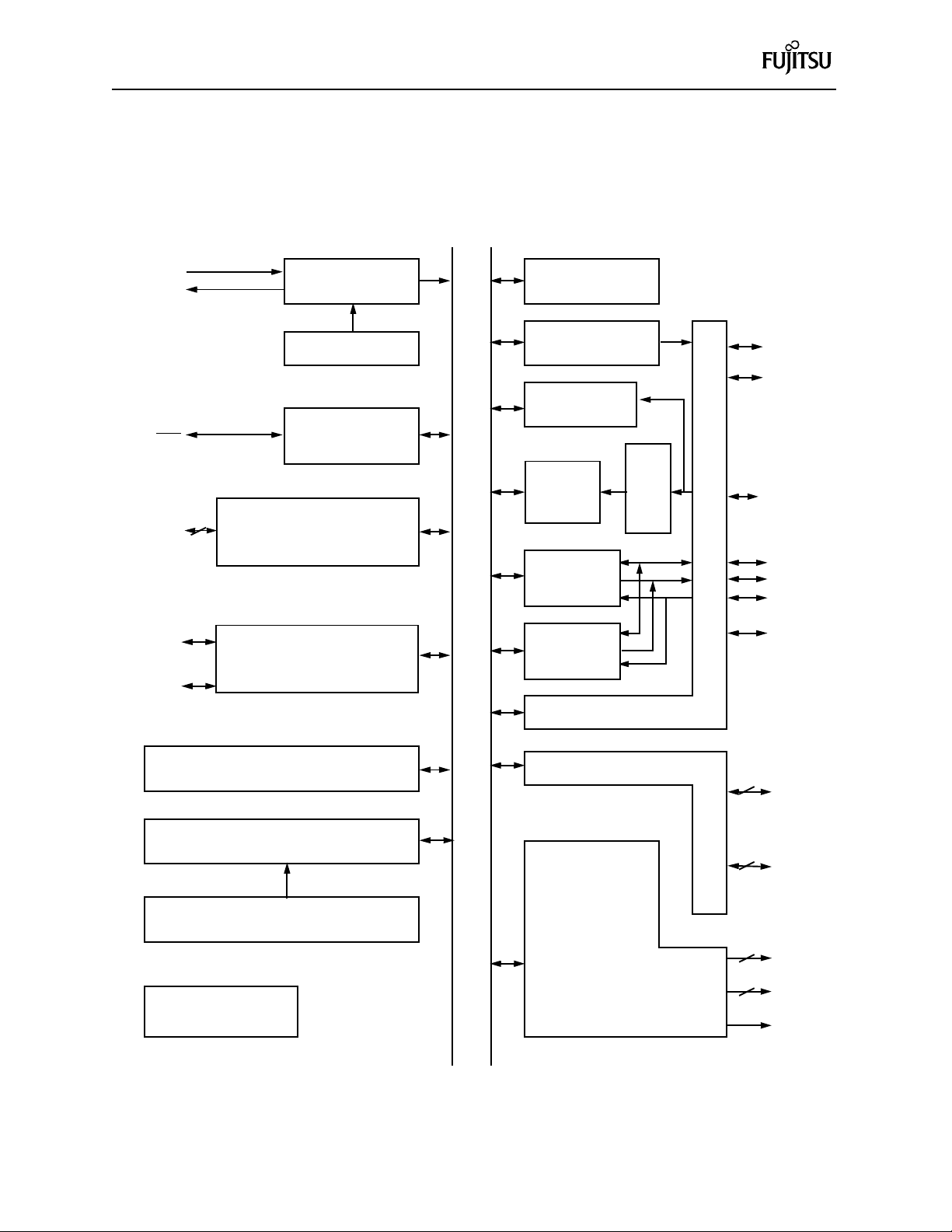
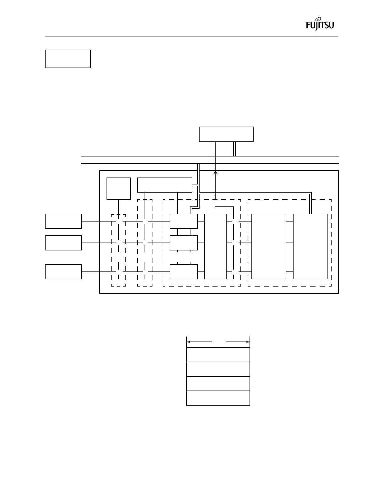
1.3 Block Diagram
GENERAL
Internal bus
RST
P20 to P25/
SEG36 to
SEG41
P30, P31
P33/V2
P32/V1
X0
X1
Main oscillator
circuit
Clock control
Reset circuit
(WDT)
Port 2
6
N-ch open-drain I/O port
Port 3
N-ch open-drain I/O port
Time-base timer
8-bit PWM timer
External interrupt
8-bit
pulse width
count timer
8-bit serial
UART
CMOS I/O port
Noise
clear
Port
4
P41/PWM
P40
P42/PWC/
INT1
P45/SCK
P44/SO
P43/SI
P46/INT0
R A M (256 × 8 bits)
F
CPU
R O M (8 K × 8 bits)
Other pins
MODA
V
, VSS
CC
2
MC-8L
N-ch open-drain I/O port
LCD controller driver
Fig. 1.1 Block Diagram (MB89953)
1– 5
Port
0/1
8
P00/SEG20 to
P07/SEG27
8
P10/SEG28 to
P17/SEG35
20
SEG0 to
SEG19
4
COM0 to
COM3
V3
Page 10
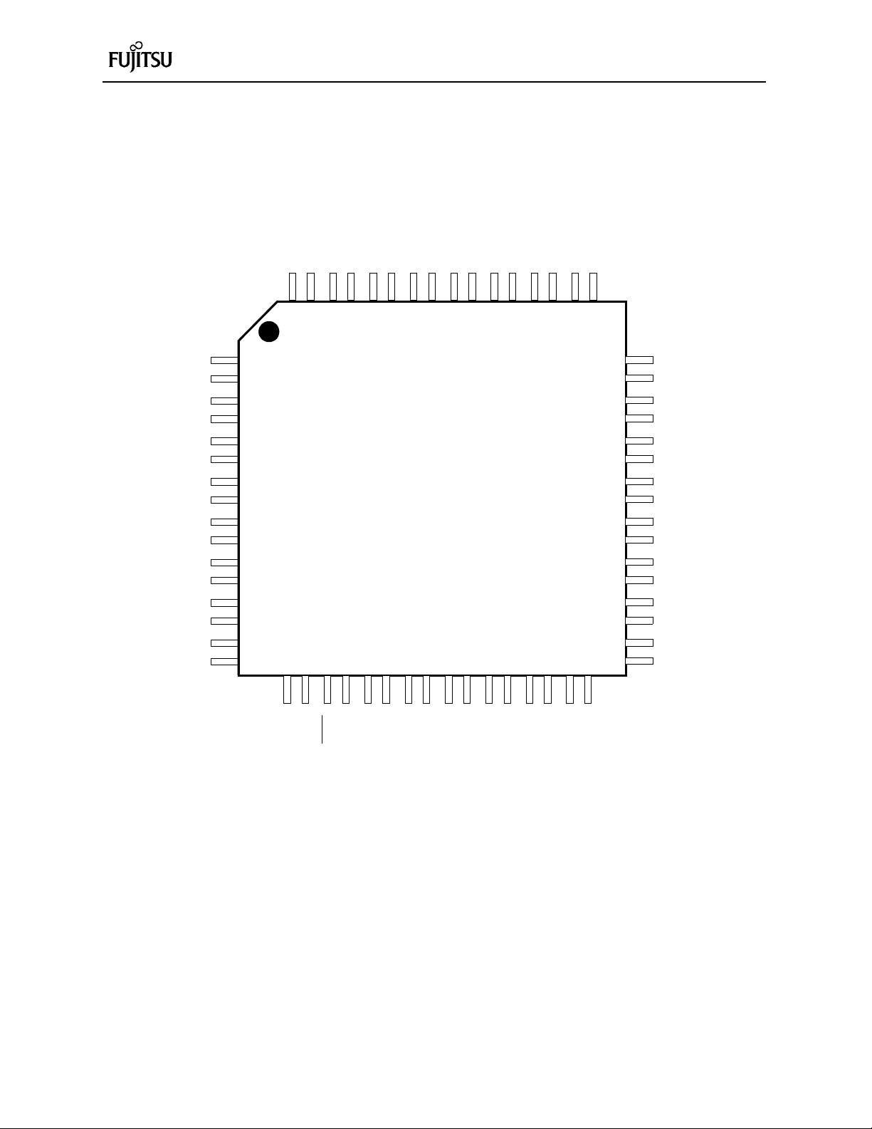
1.4 Pin Assignment
SEG5
SEG6
SEG7
SEG8
GENERAL
SEG9
SEG10
SEG11
SEG12
VCCSEG13
SEG14
SEG15
SEG16
SEG17
SEG18
SEG19
SEG4
SEG3
SEG2
SEG1
SEG0
COM3
COM2
COM1
COM0
V3
P33/V2
P32/V1
P31
P30
P40
P41/PWM
1
2
3
4
5
6
7
8
9
10
11
12
13
14
15
16
646362616059585756555453525150
Top view
QFP-64
171819202122232425262728293031
X1
V
SS
P45/SCK
P46/INT0
P25/SEG41
P24/SEG40
P23/SEG39
P22/SEG38
P21/SEG37
RST
P43/SI
P42/INT1/PWC
X0
MODA
P44/SO
32
P20/SEG36
49
48
47
46
45
44
43
42
41
40
39
38
37
36
35
34
33
P00/SEG20
P01/SEG21
P02/SEG22
P03/SEG23
P04/SEG24
P05/SEG25
P06/SEG26
P07/SEG27
P10/SEG28
P11/SEG29
P12/SEG30
P13/SEG31
P14/SEG32
P15/SEG33
P16/SEG34
P17/SEG35
Fig. 1.2 Pin Assignment of MB89953 and MB89P955 (QFP-64, pitch: 0.65 mm)
1– 6
Page 11
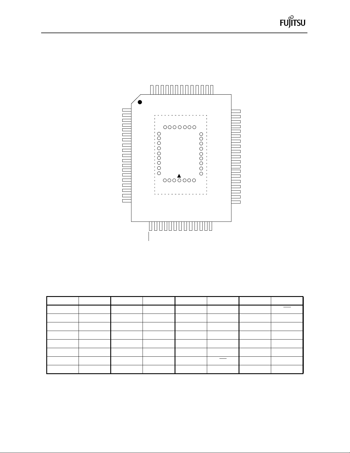
GENERAL
SEG6
SEG7
SEG8
SEG9
SEG10
SEG11
SEG12
Vcc
SEG13
SEG14
SEG15
SEG16
SEG17
64636261605958575655545352
SEG5
SEG4
SEG3
SEG2
SEG1
SEG0
COM3
COM2
COM1
COM0
V3
V2/P33
V1/P32
P31
P30
P40
PWM/P41
INT1/PWC/P42
SI/P43
1
2
3
4
5
6
7
8
9
10
11
12
13
14
15
16
17
18
19
84838281807978
85
86
87
88
89
90
91
92
93
94959665666768
(Top View)
20212223242526272829303132
X0
X1
RST
SO/P44
Vss
MODA
SCK/P45
51
50
49
48
SEG38/P22
47
46
45
44
43
42
41
40
39
38
37
36
35
34
33
SEG37/P21
77
76
75
74
73
72
71
70
69
INT0/P46
SEG41/P25
SEG40/P24
SEG39/P23
SEG18
SEG19
SEG20/P00
SEG21/P01
SEG22/P02
SEG23/P03
SEG24/P04
SEG25/P05
SEG26/P06
SEG27/P07
SEG28/P10
SEG29/P11
SEG30/P12
SEG31/P13
SEG32/P14
SEG33/P15
SEG34/P16
SEG35/P17
SEG36/P20
Fig. 1.3 Pin Assignment of MB89PV950 (MQFP-64, pitch: 0.8 mm)
Pin assignment on package top (MB89PV950 only
)
Pin No. Pin Name Pin No. Pin Name Pin No. Pin Name Pin No. Pin Name
65 N.C. 73 A2 81 N.C. 89 OE
66 Vpp 74 A1 82 O4 90 N.C.
67 A12 75 A0 83 O5 91 A11
68 A7 76 N.C. 84 O6 92 A9
69 A6 77 O1 85 O7 93 A8
70 A5 78 O2 86 O8 94 A13
71 A4 79 O3 87 CE
95 A14
72 A3 80 Vss 88 A10 96 Vcc
N.C.: Non connection pin. Keep open.
1– 7
Page 12
GENERAL
1.5 Pin Description
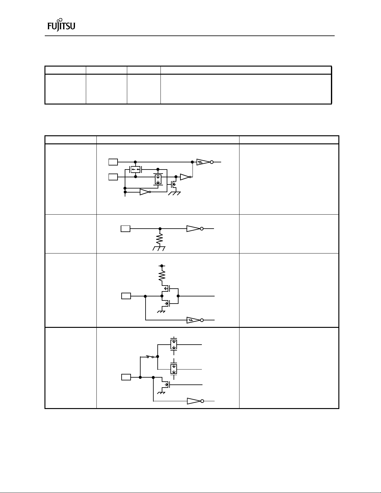
Table 1–2 lists the pin functions and shows the Fig. 1.4 input/output circuits.
T able 1–2 Pin Description
Pin No
0.65 0.8
22 23
23 24
21 22
19 20
48 to 41 49 to
42
40 to 33 41 to
34
32 to 27 33 to
28
14 to 11 15 to
12
12 to 11 13 to
12
15 16
16 17
17 18
18 19
20 21
25 26
Pin Name Circuit Function
X0 A Clock oscillator pins
X1
MODA B Operation-mode select pins
RST
P00/SEG20
to
P07/SEG27
P10/SEG28
to
P17/SEG35
P20/SEG36
to
P25/SEG41
P30 to P31 F N-channel open-drain type general-purpose I/O ports
P32/V1 to
P33/V2
P40 E General-purpose I/O ports
P41/PWM E General-purpose I/O port
P42/PWC/
INT1
P43/SI E General-purpose I/O port
P44/SO E General-purpose I/O port
P45/SCK E General-purpose I/O port
C Reset I/O pin
D N-channel open-drain type general-purpose I/O ports
D N-channel open-drain type general-purpose I/O ports
D N-channel open-drain type general-purpose I/O ports
D N-channel open-drain type general-purpose I/O ports
E General-purpose I/O port
This pin is connected directly to V
This pin consists of an N-ch open-drain output with a pull-up resistor and
hysteresis input. A Low l evel is pu t out from this pin. A “LOW” vo ltage o n
this port generates a RESET condition.
Also serve as LCDC controller segment outputs.
Switching between port output and segment output is performed by the
mask option every 8 bits.
Also serve as LCDC controller segment outputs.
Switching between port output and segment output is performed by the
mask option.
Also serve as LCDC controller segment outputs.
Switching between port output and segment output is performed by the
mask option.
Also serve as LCDC controller power supply.
A pull-up resistor option is provided.
Serves as PWM timer toggle output (PWM).
A pull-up resistor option is provided.
Also serves as pul se-width coun t tim er input (PWC) a nd exter nal interr upt
input (INT1). The PWC and INT1 inputs are hysteresis type. A pull-up
resistor option is provided.
Also serves as serial I/O and UART data input (SI). The SI input is
hysteresis type.
A pull-up resistor option is provided.
Also serves as serial I/O and UART data output (SO).
A pull-up resistor option is provided.
Also serves as serial I/O and UART clock input/output (SCK). The SCK
input is hysteresis type.
A pull-up resistor option is provided.
SS
with pull down resistor.
1– 8
Page 13
GENERAL
Pin No
0.65 0.8
26 27
5 to 1
64 to 57
55 to 49
9 to 6 7 to 10
10 11
56 57
24 25
6 to 1
64 to
58
56 to
50
Table 1–2 Pin Description
Pin Name Circuit Function
P46/INT0 E General-purpose input port
Also serves as external-interrupt input (INT0).
The input is hysteresis type.
A pull-up resistor option is provided.
SEG0 to
G For LCDC controller segment ouput
SEG19
COM0 TO
COM3
V3 - For LCD driver power supply
Vcc - Power Pin
Vss - Power (GND) Pin
G For LCDC controller common output
(Continued)
T able 1–3 Pin Description for External ROM
• External EPROM pins (for MB89PV950)
Pins No. Pin Name I/O Function
66 Vpp O For High-level output
67 A12
68 A7
69 A6
70 A5
71 A4
72 A3
73 A2
74 A1
75 A0
77 O1
79 O3
80 Vss O For power supply (GND)
82 04
83 O5
84 O6
85 O7
86 O8
87 CE
88 A10 O For address output
89 OE O
91 A11
93 A8
94 A13
95 A14
96 Vcc O For EPROM power supply
O For address output
I For data input78 O2
I For data input
O
O For address output92 A9
O For address output
For ROM out put enable
The High level is output in standby mode .
For ROM output enable.
The Low level is always output.
1– 9
Page 14
GENERAL
Table 1–3 Pin Description for External ROM
(Continued)
• External EPROM pins (for MB89PV950)
Pins No. Pin Name I/O Function
65
76
81
90
N.C. —
For internal connection
Keep open.
Fig. 1.4 I/O Circuits
Classification Circuit Remarks
A • Crystal oscillator
X1
• Feedback resistor: About 1 M
5 V (1 to 5 MHz)
X0
Standby control signal
B • CMOS input
• Pull down resistor (N-ch)
Ω
/
R
C • Output pull-up resistor (P-ch):
Ω
• About 50 M
R
P-ch
N-ch
• Hysteresis input
(5 V)
D • N-ch open-drain output
• CMOS input
N-ch
• The segment output is optional.
1– 10
Page 15
GENERAL
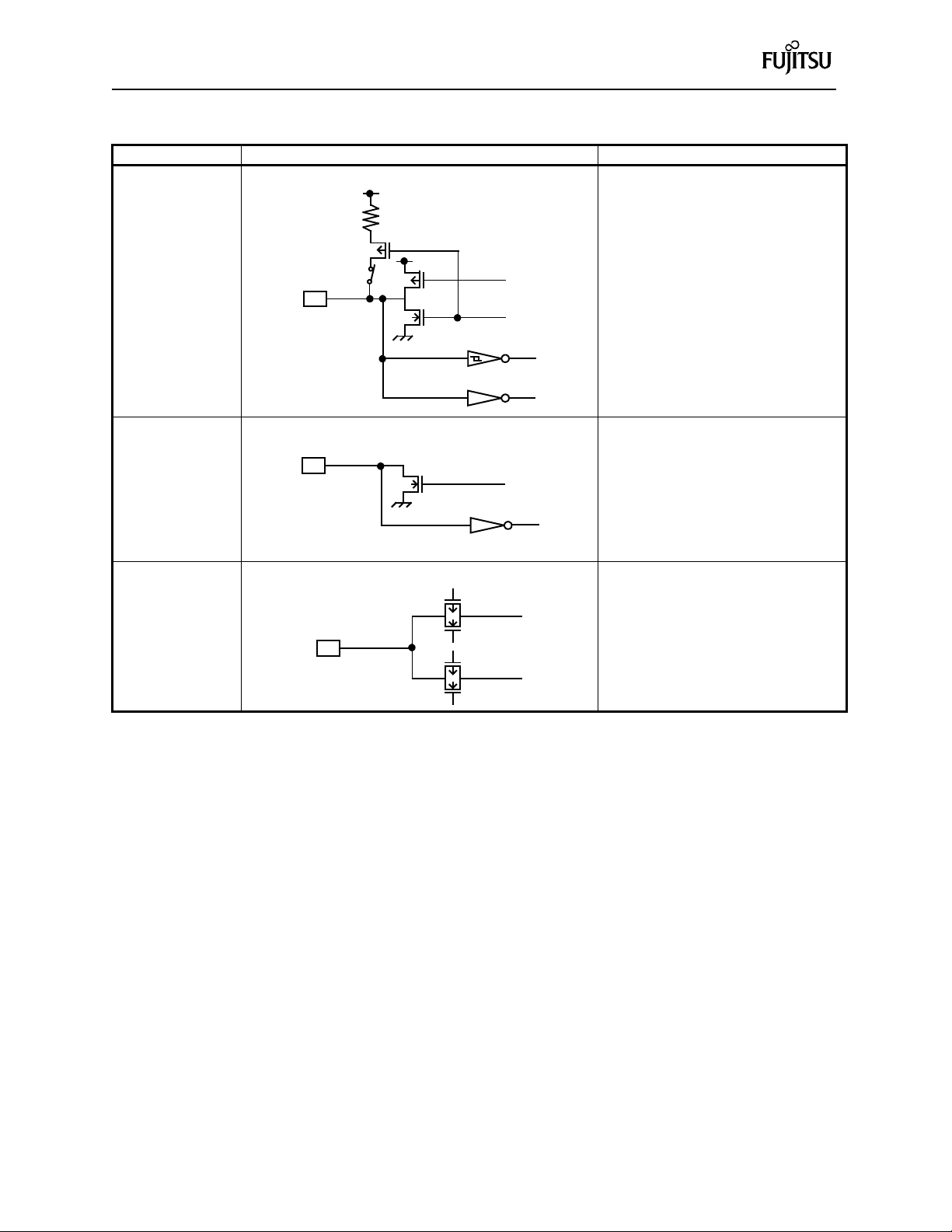
Fig. 1.4 I/O Circuits
(Continued)
Classification Circuit Remarks
E • CMOS output
• CMOS input
R
P-ch
P-ch
N-ch
• Hysteresis input
(peripheral input)
• The pull-up resistor is optional.
F • N-ch open-drain output
• CMOS input
N-ch
G • LCDC output
1– 11
Page 16
1.6 Handling Devices
(1) Preventing latch-up
GENERAL
Latchup may occur on CMOS ICs if voltage higher than V
or lower than VSS is applied to input and output
CC
pins other than medium to high-voltage pins or if higher than the voltage which shows on Absolute Maximum
Ratings is applied between V
and VSS.
CC
When latch-up occurs, supply current increases rapidly and might thermally damage elements. When using,
take great care not to exceed the absolute maximum ratings.
(2) Treatment of Unused Input Pins
Leaving unused input pins open could cause malfunctions. They should be connected to pull-up or pulldown resistor.
(3) Power Supply Voltage Fluctuations
Although V
power supply voltage is assured to operate within the rated, a rapid change to the IC is therefore
CC
cause malfunctions, ev en if it occurs within the rated range. Stabilizing voltage supplied of the IC is therefore
important. As stabilization guidelines, it is recommended to control power so that V
(P-P. value) will be less that 10% of the standard V
value at the commercial frequency (50 to 60 Hz) and
CC
ripple fluctuations
CC
the transient fluctuation rate will be less than 0.1 V/ms at the time of a momentary fluctuation such as when
power is switched.
(4) Precaution When Using an External Clock
Even when an external clock is used, oscillation stabilization time is required for power-on reset (option
selection) and release from stop mode.
(5) Recommended Screening Conditions
The OTPROM product should be screened by high-temperature aging before mounting.
Verify program
High-temperature aging (150°C, 48H)
Read
Mount
The programming test cannot be performed for all bits of the preprogrammed OTPROM product due to its
characteristics. Consequently, 100% programming yielding cannot be ensured.
1– 12
Page 17

2. HARDWARE CONFIGURATION
2.1 CPU ... ...................................................................................2-3
2.2 Peripherals .......................................................................... 2-18
Page 18
HARDWARE CONFIGURATION
This chapter describes each block of the CPU hardware.
CPU
0000
0080
00C0
0100
0140
H
H
H
H
Register
H
MB89951
I/O
Reserved
RAM
2.1 CPU
This section describes the memory space and register composing CPU
hardware.
2.1.1 Memory Space
F2MC-8L CPU has a memory space of 64 Kilobytes. All I/O, data, and
program areas are located in this space. The I/O area is near the lowest
address and the data area is immediately above it. The data area can be
divided into register, stack, and direct-address areas according to the
applications. The program area is located near the highest address, and
the tables of interrupt and reset vectors and vector-call instructions are at
the highest address in this area. Fig.2.1 shows the structure of the
memory space for the MB89950 series of microcontrollers.
MB89PV950
H
H
H
Register
H
I/O
RAM
0000
0080
0100
0180
H
H
H
Register
H
MB89953
I/O
RAM
0000
0080
0100
0200
0280
H
H
H
Register
H
H
MB89P955
I/O
RAM
0000
0080
0100
0200
F000
0480
H
Vacant
E000
H
ROM
Vacant
C000
H
ROM
Vacant
8000
H
ROM
Vacant
H
ROM
Fig. 2.1 Memory Space of MB89950 Series Microcontrollers
2– 3
Page 19
HARDWARE CONFIGURATION
CPU
(1) I/O area
This area is where various peripherals such as control and data registers
are located. The memory map for the I/O area is given in APPENDIX A.
(2) RAM area
This area is where the static RAM is located. Addresses from
017F
(
H
0100
H
to
013F
in MB89951,
H
0100
to
H
01FF0
in MB89P955 and
H
0100
H
to
MB89PV950) are also used as the general-purpose register area. One can
access these registers through register-related instructions or just treat
them as ordinary RAM.
(3) ROM area
This area is wh ere the in ternal ROM is locate d. Addres ses from
are also used for the table of interrupt, reset and vector-call
FFFF
H
FFC0
H
to
instructions. T able 2–1 shows the correspondence between each interrupt
number or reset and the table addresses to be referenced for the MB89950
series of microcontrollers.
Table 2–1 Table of Reset and Interrupt Vectors
CALLV #0
CALLV #1
CALLV #2
CALLV #3
CALLV #4
CALLV #5
CALLV #6
CALLV #7
Table address
Upper data Lower data
FFC0
FFC2
FFC4
FFC6
FFC8
FFCA
FFCC
FFCE
H
H
H
H
H
H
H
H
FFC1
FFC3
FFC5
FFC7
FFC9
FFCB
FFCD
FFCF
H
H
H
H
H
H
H
H
Interrupt #B
Interrupt #A
Interrupt #9
Interrupt #8
Interrupt #7
Interrupt #6
Interrupt #5
Interrupt #4
Interrupt #3
Interrupt #2
Interrupt #1
Interrupt #0
Reset mode
Reset vector
FFFC
Note:
FFFD
is already reserved . W hen using
H
in the reset mode, write
H
Table address
Upper data Lower data
00
FFE5
FFE7
FFE9
FFEB
FFED
FFEF
FFF1
FFF3
FFF5
FFF7
FFF9
FFFB
FFFF
.
H
H
H
H
H
H
H
H
H
H
H
H
H
H
H
FFE4
H
FFE6
H
FFE8
H
FFEA
H
FFEC
H
FFEE
H
FFF0
H
FFF2
H
FFF4
H
FFF6
H
FFF8
H
FFFA
H
----- FFFD
FFFE
H
2– 4
Page 20
HARDWARE CONFIGURATION
CPU
Before execution
A
1234
2.1.2 Arrangement of 16-bit Data in Memory Space
When the MB89950 series of microcontrollers handle 16-bit data, the data
written at the lower address is treated as the upper 8-bit data and that written
at the next address is treated as the lower 8-bit data as shown in Fig. 2.2.
Memory
MOVW ABCDH , A
ABCF
H
ABCE
H
ABCD
ABCC
H
H
H
Fig. 2.2 Arrangement of 16 bit Data in Memory Space
This is the same when 16 bits are specified by the operand during execution
of an instruction. Bits closer to the OP code are treated as the upper byte
and those next to it are treated as the lower byte. This is also the same
when the memory address or 16-bit immediate data is specified by the
operand.
After execution
1234
A
Memory
ABCF
H
34
H
ABCE
H
12
H
ABCD
ABCC
H
H
H
[Example]
MOV A, 5678
MOV A, #1234
; Extended address
H
; 16-bit immediate data
H
Assemble
XXXXH XX XX
60 56 78
XXXX
XXXX
XXXX
H
H
H
E4 12 34
XX
; Extended address
; 16-bit immediate data
Fig. 2.3 Arrangement of 16 bit Data during Execution of Instruction
Data saved in the stack by an interrupt is also treated in the same manner.
2– 5
Page 21
HARDWARE CONFIGURATION
CPU
2.1.3 Internal Registers in CPU
The MB89950 series of microcontrollers have dedicated registers in the
CPU and general-purpose registers in memory. The types of dedicated
registers are as follows.
•
Program counter (PC) 16-bit length register indicating the location
where instruction s ar e stored .
•
Accumulator (A) 16-bit length register storing results of
operations temporarily. The lower one byte
is used to execute 8-bit data processing
instructions.
•
Temporary accumulator (T) 16-bit length register where the operations
are performed between this register and the
accumulator. The lower one byte is used to
execute 8-bit data processing instructions.
•
Index register (IX) 16-bit length register for index modification.
•
Extra pointer (EP) 16-bit length register for indicating memory
address.
•
Stack pointer (SP) 16-bit length register indicating stack area.
•
Processor status (PS) 16-bit length register where register
pointers and condition codes are stored.
16 bits
P C
A
T
IX
EP
SP
PS
Program counter
Accumulator
Temporary accumulator
Index register
Extra pointer
Stack pointer
Processor status
2– 6
Page 22
HARDWARE CONFIGURATION
CPU
for a register bank pointer (RP) and 8 lower bits for a condition code register
(CCR). (See Fig. 2.4.)
The 16 bits of the processor status (PS) can be divided into 8 upper bits
1514131211109876543210
PS
RP
Vacant Vacant Vacant
RP
HI NZVC
IL1, 0
CCR
Fig. 2.4 Structure of Processor Status
The RP indicates the address of the current register bank. The relationship
between the contents of the RP and the real addresses is as shown in
Figure 2.5.
Source address
R P
‘0’ ‘0’ ‘0’ ‘0’ ‘0’ ‘0’ ‘0’ ‘1’ R4 R3 R2 R1 R0 b2 b1 b0
↓↓↓↓↓↓↓↓↓↓↓↓↓↓↓↓
A15 A14 A13 A12 A11 A10 A9 A8 A7 A6 A5 A4 A3 A2 A1 A0
Lower bits of OP code
Fig. 2.5 Rule for Translating Real Addresses at General-purpose Register Area
The CCR has bits indicating the results of operations and transfer data
contents, and bits controlling the CPU operation when an interrupt occurs.
- H-flag H-flag is set when a carry or a borrow out of bit 3 into bit 4
is generated as a result of operations; it is cleared in other
cases. This flag is used for decimal-correction instructions.
- I-flag An interrupt is enabled when this flag is 1 and is disabled
when it is 0. The I-flag is 0 at reset.
- IL1 and IL0 These bits indicate the level of the currently-enabled
interrupt. The CPU executes interrupt processing only when
an interrupt with a value smaller than the value indicated by
this bit is requested.
IL1 IL0 Interrupt level High and low
00
1
High
01
10 2
11 3
low = No interrupt
- N-flag The N-flag is set when the most significant bit is 1 as a result
of operations; it is cleared when the MSB is 0.
2– 7
Page 23
HARDWARE CONFIGURATION
CPU
- Z-flag Z-flag is set when zero is the result of operations; it is
cleared in other cases.
- V-flag V -flag is set when a two’s complement overflow occurs as a
result of operations; it is reset when an overflow does not
occur.
- C-flag C-flag is set when a carry or a borrow out of bit 7 is generated
as a result of operations; it is cleared in other cases. When
the shift instruction is executed, the value of the C- flag is
shifted out.
•
General-purpose register..... 8-bit length register where data are stored.
8-bit general-purpose registers are provided in the register banks in the
memory for storing data. Eight registers are provided per bank for and up
to 16 banks can be used for MB89953 (8 banks are provided in MB89951,
32 banks are provided in MB89P955 and MB89PV950).
The register bank pointer (RP) indicates the currently-used bank.
Note: The register banks are as follows depend on RAM area.
MB89951
MB89953
MB89P955
MB89PV950
0100
0100
0100
0100
H
H
H
H
to
to
to
to
013F
017F
01FF
01FF
8 banks
H
16 banks
H
32 banks
H
32 banks
H
Address =
0100
+ 8*(RP)
H
Memory area
Fig. 2.6 Register Bank Configuration
R0
R1
R2
R3
R4
R5
R6
R7
16 banks
2– 8
Page 24
HARDWARE CONFIGURATION
CPU
Clock
oscillator
2.1.4 Clock Control Block
This block controls the standby operation and software reset.
(1) Machine clock control block diagram
(a) Machine clock control section
STP SLP SPL
Pin state
Stop
CPU operation clock
Clock control
Peripheral operation clock
From time-base timer
Power-on reset
Watchdog timer reset
External reset
Software reset
HC1
HC3
Stop release signal
Selector
Option
(b) Reset control section
Reset control
(2) Register list
Address:
0008
H
8 bits
STBC
Internal reset signal
Standby control register
2– 9
Page 25
HARDWARE CONFIGURATION
CPU
0008
(3) Description of registers
The detail of each register is described below.
STBCAddress:
H
(a) Standby control register (STBC)
Bit 7 Bit 6 Bit 5 Bit 4 Bit 3 Bit 2 Bit 1 Bit 0
Address:
0008
STPSLPSPLRST————
H
(W) (W) (R/W) (W )
(Initial value)
0001XXXX
[Bit 7] STP: Stop bit
This bit is used to specify switching CPU to the stop mode.
0
1
No operation
Stop mode
This bit is cleared at reset or stop cancellation.
0 is always read when this bit is read.
[Bit 6] SLP: Sleep bit
This bit is used to specify switching the CPU to the sleep mode.
0
1
No operation
Sleep mode
This bit is cleared at reset, sleep cancellation or stop cancellation.
0 is always read when this bit is read.
[Bit 5] SPL: Pin state specifying bit
This bit is used to specify the external pin state in the stop mode.
0
1
Holds pin state and level immediately before stop mode
High impedance
This bit is cleared at reset.
[Bit 4] RST: Software reset bit
This bit is used to specify the software reset.
0
1
Generates 4-cycle reset signal
No operation
1 is always read when this bit is read.
2– 10
Page 26
HARDWARE CONFIGURATION
CPU
(4) Description of operation
(a) Low-power consumption mode
This chip has three operation modes shown in the table below. The sleep
mode and stop mode reduce the power consumption. The system clock
can be selected out of three according to the system condition to minimize
power consumption.
Table 2–2 Operating Mode of Low-power Consumption Modes
Each operating clock pulse
Oscillation
mode
RUN
SLEEP
STOP Stop Stops Stops External interrupt
Clock
pulse
Oscillates
CPU
2.5 MHz
Stops
(5 MHz clock)
Time-base
timer
2.5 MHz 2.5 MHz
peripheral
Each
Wake-up source
in each mode
Various interrupt
requests
• The SLEEP mode stops only the operating clock pulse of the CPU; other
operations are continued.
• The STOP mode stops the oscillation. Data can be held with the lowest
power consumption in this mode.
a. SLEEP mode
• Switching to Sleep mode
- Writing 1 at the SLP (bit 6) of the STBC register switches the mode to
SLEEP mode.
- The SLEEP mode is the mode to stop clock pulse operating the CPU;
only the CPU stops and the peripherals continue to operate.
- If an interrupt is requested when 1 is written at the SLP (bit 6),
instruction ex ecution continues without switching to the SLEEP mode.
- In the SLEEP mode, the contents of registers and RAM immediately
before entering the SLEEP mode are held.
• Canceling SLEEP mode
- The SLEEP mode is canceled by inputting the reset signal or
requesting an interrupt.
- When the reset signal is input during the SLEEP mode, the CPU is
switched to the reset state and the SLEEP mode is canceled.
- When an interrupt level higher than 11 is requested from a peripheral
during the SLEEP mode, the SLEEP mode is canceled.
- When the I flag and IL bit are enable after canceling, the CPU executes
the interrupt processing like an ordinary interrupt. When they are
disabled, the CPU starts processing the next instruction given before
entering the SLEEP mode.
2– 11
Page 27

HARDWARE CONFIGURATION
CPU
b. STOP mode
• Switching to STOP mode
- Writing 1 at the STP (bit 7) of the STBC register switches the mode to
STOP mode.
- The STOP mode stops clock oscillation and the CPU and all
peripherals stop.
- The input/output pins and output pins in the STOP mode can be
controlled by the SPL (bit 5) of the STBC register so that they are held
in the state immediately before entering the STOP mode, or so that
they enter in the high-impedance state.
- If an interrupt is requested when 1 is written at the STP (bit 7),
instruction execution continues without switching to the STOP mode.
- In the STOP mode, the contents of registers and RAM immediately
before entering the STOP mode are held.
• Canceling STOP mode
- The STOP mode is canceled either by inputting the reset signal or by
requesting an interrupt.
- When the reset signal is input during the STOP mode, the CPU is
switched to the reset state and the STOP mode is canceled.
- When an interrupt higher than level 11 is requested from the external
interrupt circuit during the STOP mode, the STOP mode is canceled.
- When the I flag and IL bit are enabled after canceling, the CPU
executes the interrupt processing like an ordinary interrupt. When they
are disabled, the CPU starts processing the next instruction given
before entering the STOP mode.
- The oscillation stabilization time can be selected from the two types
in Table 2–3 as options.
- If the STOP mode is canceled by inputting the reset signal, the CPU
is switched to the oscillation stabilization state. Therefore, the reset
sequence is not executed unless the oscillation stabilization time is
elapsed. The oscillation stabilization time corresponds to the
optionally selected oscillation stabilization time of the main clock.
However, when Power-on reset unavailable is selected by the mask
option, the CPU is not switched to the oscillation stabilization state
even if the STOP mode is canceled by inputting the reset signal.
Table 2–3 Selection of Oscillation Stabilization Time
Oscillation
stabilization time
18
14
/f
CH
/f
CH
About 2
About 2
Oscillation stabilization
Remarks
time at 5 MHz
About 52.4 ms For crystal oscillator
About 3.28 ms For crystal oscillator
2– 12
Page 28
HARDWARE CONFIGURATION
CPU
(b) State transition diagram
STOP
Clock stops.
(8)
(3)
Oscillation stabilization
waiting
(7)
SLEEP
Clock oscillates.
(5)
(4)
Clock oscillates.
(9)
RUN
(1) (2)
Power-on
(1) When power-on reset available selected
(2) When power-on reset unavailable selected
(3) After oscillation stabilizing
(4) Set STP bit to 1.
(5) Set SLP bit to 1.
(7) External reset when power-on reset unavailable selected
(8) External reset or interrupt when power-on reset available selected
(9) External reset or interrupt
2– 13
Page 29
HARDWARE CONFIGURATION
CPU
(c) Reset
There are four types of reset depending on the source shown in Table 2–4.
Table 2–4 Sources of Reset
Reset name Description
External-pin reset
Software reset
Watchdog reset
Power-on reset
When the power-on reset or reset during the stop state is used, the
oscillation stabilization time is needed after the oscillator starts operating.
The time-base timer controls this stabilization time. Consequently, the
operation does not start immediately even after canceling the reset.
Howev er, if P ower-on reset is not selected by the mask option, no oscillation
stabilization time is required in any state after external pins have been
released from the reset.
When setting external-reset pin to Low
When writing 0 at RST (bit 4) of STBC
When watchdog timer overflows
When turning power on
Note: A longer time than the optionally-specified oscillation stabilization
time should be allowed for reset at power-on of P ower-on reset
unavailable products. In other cases, the time is based on theorist
timing given in the
characteristics.”
MB89950 SERIES DATA SHEET
“AC
2– 14
Page 30
HARDWARE CONFIGURATION
CPU
Peripheral #1
F2MC-8L bus
Test
register
G L
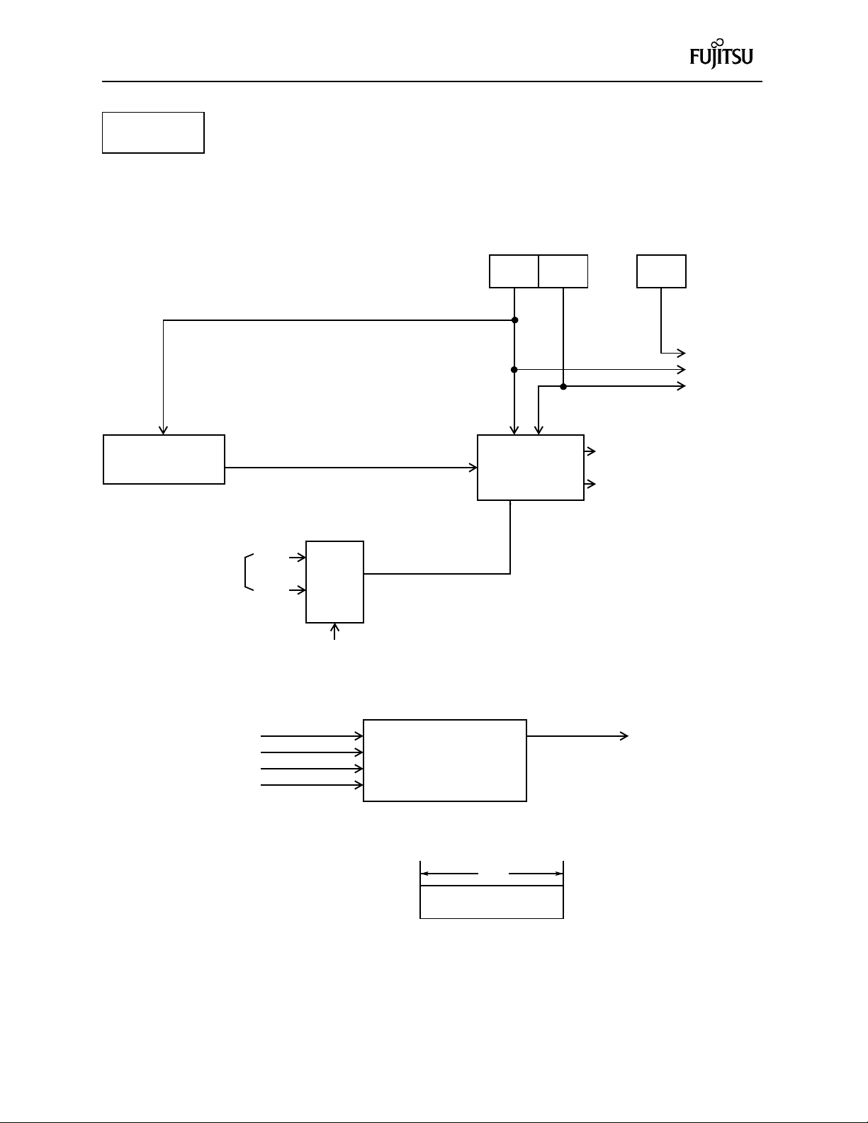
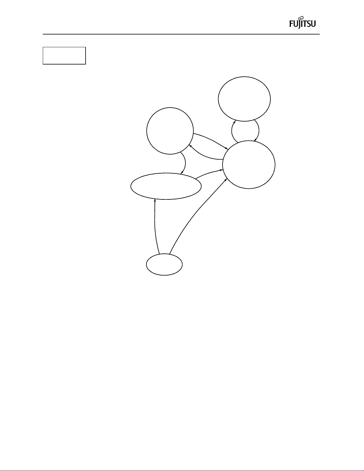
2.1.5 Interrupt Controller
The interrupt controller for the F2MC-8L family is located between the CPU
and each peripheral. This controller receives interrupt requests from the
peripherals, assigns priority to them. When the interrupt controller transfers
the priority to the CPU, it also decides the priority of same-level interrupts.
(1) Block diagram
CPU
2
Address decoder
Level
G
Peripheral #2
•
•
Peripheral #n
G
•
•
•
G
L
•
•
•
L
Level
•
•
•
Level
•
•
•
Level
deciding
block
G
G
Same level
priority
deciding
block
Interrupt
vector
generation
•
block
•
•
(2) Register list
Interrupt controller consists of interrupt-level registers (ILR1, 2, and 3) and
interrupt-test register (ITR).
8 bits
Address:
Address:
Address:
Address:
007C
007D
007E
007F
H
H
H
H
ILR1
ILR2
ILR3
ITR
W Interrupt level register #1
W Interrupt level register #2
W Interrupt level register #3
— Interrupt test register
2– 15
Page 31

HARDWARE CONFIGURATION
CPU
Address:
Address:
Address:
Address:
[Example]
007C
007D
007E
007F
Interrupt requests
from peripherals
ILR1
H
ILR2
H
ILR3
H
ITR
H
(3) Description of registers
The details of each register is described below.
(a) Interrupt level register 1 to 3 (ILRx: Interrupt Level Register x)
Bit 7 Bit 6 Bit 5 Bit 4 Bit 3 Bit 2 Bit 1 Bit 0
Address:
Address:
Address:
007C
007D
007E
L31 L30 L21 L20 L11 L10 L01 L00
H
L71 L70 L61 L60 L51 L50 L41 L40
H
LB1 LB0 LA1 LA0 L91 L90 L81 L80
H
(W) (W) (W) (W) (W ) (W) (W) (W)
(Initial value)
11111111
B
The ILRx sets the interrupt level of each peripheral. The digits in the center
of each bit correspond to the interrupt numbers.
MB89820 hardware manual
L3X
Interrupt control module
IR0
IR1
IR2
IR3
IRB
Interrupt
number
#0
#1
#2
#3
#11
Table address
Upper Lower
FFFA
FFF8
FFF6
FFF4
FFE4
FFFB
FFF9
FFF7
FFF5
FFE5
007C
007D
007E
007F
[Bits 7 and 6][Bits 5 and 4][Bits 3 and 2][Bits 1 and 0]Lx1, Lx0: Interrupt
level setting bit
Lx1 Lx0 Required interrupt level
0
1
1
X
0
1
1
2
3 (None)
When an interrupt is requested from a peripheral, the interrupt controller
transfers the interrupt level based on the value set at the 2 bits of the ILRx
corresponding to the interrupt to the CPU.
(b) Interrupt test register (ITR)
ILR1Address:
H
ILR2Address:
H
ILR3Address:
H
ITRAddress:
H
Address:
007F
The ITR is used for testing. Do not access it.
Bit 7 Bit 6 Bit 5 Bit 4 B it 3 Bit 2 Bit 1 Bit 0
——————
H
(Initial value)
XXXXXX00
B
**
(—) (—)
2– 16
Page 32

HARDWARE CONFIGURATION
CPU
(4) Description of operation
The functions of interrupt controllers are described below.
(a) Interrupt functions
The MB89950 series of microcontrollers have 7 inputs for interrupt requests
from the peripherals. The interrupt level is set by 2-bit registers
corresponding to each input. When an interrupt is requested from a
peripheral, the interrupt controller receives it and transfers the contents of
the correspo ndi ng level register to the C PU. The interrupt to the de vice is
processed as follows:
(1) An interrupt source is generated inside a peripheral.
(2) If an interrupt is enabled after referring to the interrupt-enable bit
inside the peripheral, an interrupt request is output from the
peripheral to the interrupt controller.
(3) After receiving this interrupt request, the interrupt controller
determines the priority of simultaneously-requested interrupts and
then transfers the interrupt level for the applicable interrupt to the
CPU.
(4) The CPU compares the interrupt level requested from the interrupt
controller with the IL bi t in the processor status register.
(5) As a result of the comparison, if the interrupt level has priority over
the current interrupt processing level, the contents of the I-flag in the
same processor status register are checked.
(6) As a result of the check in step (5), if the I-flag is enabled for an
interrupt, the contents of the IL bit are set to the required level. As
soon as the currently-executing instruction is terminated, the CPU
performs the interrupt processing and transfers control to the
interrupt-processing routine.
(7) When an interrupt source is cleared by software in the user’s interrupt
processing routine, the CPU terminates the interrupt processing.
Fig. 2.7 outlines the interrupt operation for the MB89950 series of
microcontrollers.
Internal bus
Register file
IPLA IR
(6)
CPU
Peripheral
Enable FF
AND
(7)
Source FF
(1)
Peripheral
(2)
Fig. 2.7 Interrupt-processing Flowchart
2– 17
PS I IL
Check Comparator
(5) (4)
(3)
Level
comparator
Interrupt controller
Page 33

Peripherals
Pin Input Type Output
Type
P00 to
P07
P10 to
P17
P20 to
P25
P30 to
P33
P40 to
P45
CMOS N-ch
open drain
CMOS N-ch
open drain
CMOS N-ch
open drain
CMOS N-ch
open drain
CMOS CMOS
Hysteresis Timer serial/external
push-pull
HARDWARE CONFIGURATION
2.2 Peripherals
2.2.1 I/O Ports
• The MB89950 series of microcontrollers have fiv e par alle l ports (33 pins).
Ports 0 and 1 serve as 8-bit I/O ports; port 2 serves 6-bit I/O port; port
3 serves as 4-bit I/O ports; port 4 serves as 7-bit I/O port.
• Ports 0, 1, 2, 3 and 4 are also used as peripherals.
(1) List of port functions
Table 2–5 List of Port Functions
Function bit 7 bit 6 bit 5 bit 4 bit 3 bit 2 b it 1 bit 0
Parallel port 0 P07 P06 P05 P04 P03 P02 P01 P00
Segment output SEG 27
—————————————
Parallel port 1 P17 P16 P15 P14 P13 P12 P11 P10
Segment port 1 SEG 35
Parallel port 2
Parallel port 3
LCD voltage
Parallel port 4
interrupt
—————————————
——
——
————
————
—
INT0 SCK SO SI PWC
—
P25 P24 P23 P22 P21 P20
SEG41
————————
P33 P32 P31 P30
V2 V1
P46 P45 P44 P43 P42 P41 P40
/INT1
SEG20
SEG28
SEG36
——
PWM
—
Address:
Address:
Address:
Address:
Address:
Address:
0000
0002
0004
000C
000E
000F
(2) Register list
I/O port consists of the following registers.
8 bits
H
H
H
H
H
H
PDR0
PDR1
PDR2
PDR3
PDR4
DDR4
R/W Port 0 data register
R/W Port 1 data register
R/W Port 2 data register
R/W Port 3 data register
R/W Port 4 data register
W Port 4 data direction register
Initi al value = 11111111
Initi al value = 11111111
Initi al value = 11111111
Initi al value = 11111111
Initial value = XXXXXXXX
Initial value = X0000000
B
B
B
B
B
B
2– 18
Page 34

HARDWARE CONFIGURATION
Peripherals
(3) Description of functions
The function of each port is described below.
P00 to P07: N-ch open-drain type input/output ports
(also used as segment output)
P10 to P17: N-ch open-drain type input/output ports
(also used as segment output)
P20 to P25: N-ch open-drain type input/output ports
(also used as segment output)
• Operation for output port
The value written at the PDR is output to the pin. When the PDR is read,
usually, the value of the pin is read instead of the contents of the output
latch. However , when the Read Modify Write instruction is executed, the
contents of the output latch are read. Therefore, the bit-processing
instruction can be used even if input and output are mixed with each other.
• Operation for input port
When using these ports as input ports, set 1 at the PDR and turn the
output transistor off. The value of the pin can always be read when the
PDR is read. When the segment output is selected by the LCD controller
port/segment select bit, the input data is always read as 0.
• Operation for segment output
When using these ports as segment outputs, the segment output must
be selected by the mask option. When segment output is selected using
the LCD controller port/segment select bit, these ports can be used as
segment outputs.
• State at reset
At reset, these ports serve as port inputs. The PDR is initialized to 1 and
the output transistor is turned off at all bits.
• State in stop mode
For segment output, the output state when the CPU enters the stop mode
is held. For port output, the pins states in stop mode are controlled by
SPL bit in standby control register (STBC).
When SPL=0, pin states before entering stop mode are held.
When SPL=1, port pins go high impedance in stop mode.
2– 19
Page 35

Peripherals
HARDWARE CONFIGURATION
Internal-data bus
PDR
PDR read
PDR read
(when Read Modify Write instruction
executed)
Output latch
PDR write
Stop, SPL = 1
Fig. 2.8 Ports 0, 1 and 2
Note: Selection of segment output using the mask option is available only
for mass-produced products. The mask option must be consistent
with LCD segment output select register (SEGR).
Segment output select register
Stop, SPL = 1
Segment output
Mask option
(Note)
Pin
N-ch
2– 20
Page 36

HARDWARE CONFIGURATION
Peripherals
P30, P31: N-ch open-drain output, CMOS input
P32, P33: N-ch open-drain type input/output ports
(also used as LCD controller power supply V1,V2)
• Operation for output port
The value written at the PDR is output to the pin. When the PDR is read,
usually, the value of the pin is read instead of the contents of the output
latch. However , when the Read Modify Write instruction is executed, the
contents of the output latch are read. Therefore, the bit-processing
instruction can be used even if input and output are mixed with each other.
• Operation for input port
When using these ports as input ports, set 1 at the PDR and turn the
output transistor off. The value of the pin can always be read when the
PDR is read. When V1/V2 is selected by PSEL bit of LCDR, the input
data is always read as 0.
• Operation for V1 and V2
The PSEL bit in LCDR (see page 2-60) must be cleared in order to choose
P32/P33 as LCD controller power supply.
• State at reset
At reset, these ports serve as LCD controller power supply . The PDR is
initialized to 1 and the output transistor is turned off at all bits. Since PSEL
bit of LCDR will be reset to zero (see page 2-60), therefore P32/P33 will
be configured to V1/V2 right after reset.
• State in stop mode
If P32/P33 is chosen as V1/V2 and stop mode is triggered, the voltage
at those pins before stop mode will be held. For port output, the pins
states in stop mode are controlled by SPL bit in standby control register
(STBC).
When SPL=0, pin states before entering stop mode are held.
When SPL=1, port pins go high impedance in stop mode.
2– 21
Page 37

HARDWARE CONFIGURATION
Internal-data bus
PDR
PDR read
PDR read
(when Read Modify Write instruction
executed)
Output latch
PDR write
Stop, SPL = 1
Fig. 2.9 Port 3
Only for P32 and P33
PSEL of LCDR
V1/ V2
Stop
Pin
N-ch
2– 22
Page 38

HARDWARE CONFIGURATION
Peripherals
P40 to P46: CMOS type I/O ports
(also used as peripheral input and output)
• Switching input and output
This port has a data-direction register (DDR) and a port-data register
(PDR) for each bit. Input and output can be set independently for each
bit. The pin with the DDR set to 1 is set to output, and the pin with the
DDR set to 0 is set to input. When the peripheral output bit is enabled,
these ports are set to output irrespective of the DDR setting conditions.
• Operation for output port (DDR = 1)
The value written at the PDR is output to the pin where the DDR is set
to 1. When the PDR is read, usually, the value of the pin is read instead
of the contents of the output latch. However , when the Read Modify Write
instruction is executed, the contents of the output latch are read
irrespective of the DDR setting conditions. Therefore, the bit-processing
instruction can be used even if input and output are mixed with each
other. When data is written to the PDR, the written data is held in the
output latch irrespective of the DDR setting conditions.
• Operation for input port (DDR = 0)
When used as the input port, the output impedance goes High.
Therefore, when the PDR is read, the value of the pin is read.
• Peripheral output operation
When using as the peripheral output, setting is performed by the
peripheral output enable bit (See the description of each peripheral). The
peripheral output enable bit has priority in switching input and output.
Even if the output from each peripheral is enabled, the read value of the
port is effective, so the peripheral output value can be checked.
• Peripheral input operation
The pin value at a port with the peripheral input function is always input
for the peripheral input irrespective of the setting of the DDR and
peripheral. Set the DDR to input when using an external signal for the
peripheral input.
• State when reset
When reset, the DDR is initialized to 0 and the output impedance goes
High at all bits. When reset, the PDR is not initialized. Therefore, set
the value of the PDR before setting the DDR to output.
• State in stop mode
With the SPL bit of the standby-control register set to 1, the output
impedance goes High in stop mode irrespective of the value of the DDR.
2– 23
Page 39

Peripherals
HARDWARE CONFIGURATION
External interrupt enable
Stop, SPL = 1
To external interrupt
Stop, SPL = 1
Peripheral input
Internal-data bus
PDR
PDR read
PDR read
(when Read Modify Write instruction executed)
Output latch
PDR write
DDR
DDR write
Stop, SPL = 1
Fig. 2.10 Port 4
Peripheral
output
Peripheral
output enable
Pull-up resistor
(option)
P-ch
P-ch
Pin
N-ch
2– 24
Page 40

HARDWARE CONFIGURATION
Peripherals
IRQ2
2.2.2 8-bit PWM Timer (Timer 1)
• This timer can be used as an 8-bit timer or PWM control circuit with
8-bit resolution.
• Four kinds of clock frequency can be selected.
(1) Block diagram
Internal-data bus
P/T
CNTR
P/T — P1 P0 TRE TIR 0E TIE
COMR
Start
CLK
CLEAR
OVER FLOW
Compare register
8-bit
counter
8
CPU clock pulse*
Timer-2 output
(PWC timer)
Selector
1/2
1/32
1/128
* CPU clock pulse is 1/2 oscillation.
(2) Register list
Address:
Address:
Timer/
PWM
0012
0013
8
Comparator
PWM generator and
output control
Output
enable
Output
P41/PWM
8 bits
H
H
CNTR
COMR
R/W Control register
W Compare register
signal
2– 25
Page 41

HARDWARE CONFIGURATION
Peripherals
Address:
Address:
0012H
0013H
CNTR
COMR
(3) Description of registers
(a) Control register (CNTR)
Bit 7 Bit 6 Bit 5 Bit 4 Bit 3 Bit 2 Bit 1 Bit 0
Address:
0012
P/T — P1 P0 TPE TIR OE TIE
H
(R/W) (R/W) (R/W) (R/W) (R/W) (R/W) (R/W)
(Initial value)
0X000000
B
[Bit 7] P/T: Timer/PWM operation mode switching bit
The operation is performed as the ti mer whe n bit 7 i s set to 0, and as the
0
Timer
1
PWM control circuit
When switching, set channel to stop counting (TPE = 0), interrupt disabled
(TIE = 0) and interrupt request flag cleared (TIR = 0).
[Bits 5 and 4] P1 and P0: Clock-pulse select bits
Clock pulses from the prescaler or WT0 output of timer 2 (pulse-width count
timer) can be selected using P1 and P0.
P1 P0 Clock cycle
0
0
1
1
Internal clock pulse 1 instruction cycle
0
Internal clock pulse 16 instruction cycles
1
Internal clock pulse 64 instruction cycles
0
Timer 2 cycle
1
Note that these bits must not be rewritten when the counter is operating
(TPE = 1).
[Bit 3] TPE: Counting enable bit
When these bits are set to 1, the timer or PWM control circuit starts
operation.
0
Stops counting
1
Starts counting
[Bit 2] TIR1: PWM channel interrupt request flag bit
Bit 2 goes to 1 when an interrupt source occurs. To clear the generated
interrupt source, write 0 at this bit. The meaning of bit to be read is as
follows:
2– 26
Page 42

HARDWARE CONFIGURATION
Values of counter and COMR do not match.
0
Values of counter and COMR match.
1
Peripherals
Note that 1 is always read when the Read Modify Write instruction is
executed.
The meaning of each bit to be written is as follows:
0
Clears this bit
1
Does not change this bit nor affect other bits
Note: In the PWM operation mode, neither the read nor write values of
these bits have any meaning.
[Bit 1] OE: Output signal control bit
When bit 1 is 1, the port serves as the PWM timer output. In the timer
operation mode, a signal that is reversed each time the values of the counter
and the compare register match is output. In the PWM operation mode, a
PWM signal is output.
0
General-purpose ports (P41)
1
Counter/PWM output pins (PWM)
Even if the DDR of P41 is set for input (bit 1 of DDR4 is set to 1), when this
bit is 1, it serves as the counter/PWM output pin.
Address:
Address:
0012H
0013H
CNTR
COMR
[Bit 0] TIE: Interrupt enable bit (Timer mode)
If bit 0 is set to 1, an interrupt occurs when the values of the counter and
the compare register match.
0
Disables counter interrupt output
1
Enables counter interrupt output
However, in the PWM operation mode, an interrupt does not occur
irrespective of the value of this bits.
(b) Compare register (COMR)
This register holds the value to be compared with the counter value in the
timer operation mode, and also clears the counter when the value agrees
with the counter value. In the PWM operation mode, the High pulse width
can be specified by this register value.
Bit 7 Bit 6 Bit 5 Bit 4 Bit 3 Bit 2 Bit 1 Bit 0
Address:
0013
H
(W) (W) (W) (W) (W ) (W) (W) (W)
(Initial value)
XXXXXXXX
B
2– 27
Page 43

HARDWARE CONFIGURATION
Peripherals
Count-clock pulse
TPE
P41/PWM
TIR bit setting
(4) Description of operation
(a) Timer function
Setting the P/TX bit of the CNTR to 0 gives the timer-operation mode. When
the TPE bit of the CNTR is set to 1, the counter starts incrementing from
. When the value of the counter agrees with that of the COMR, the
00
H
counter is cleared on the next count clock pulse and incrementing restarts.
Therefore, the TIR bits are set and the output pin is reversed (but, when
the TPE bit is 0, the output pin is fixed at Low level) in cycles of the count
clock pulses when
than those of the count clock pulses when
is written at the COMR, or in cycles 256 times longer
00
H
is written.
FF
H
If the value of the COMR is rewritten in the timer-operation mode, it becomes
effective from the next cycle (when the value of the counter is
, the value
00
H
of the COMR is transferred to the comparator latch).
00 00 00 00 00 01 FF 00
Value of COMR
00 FF
Fig. 2.11 Timer Operation
If the TIE bit of the CNTR is set to 1, an interrupt occurs when the values
of the counter and COMR match. During interrupt processing, the TIR bit
is used as the interrupt flag. The TIR bit is set irrespective of the value of
the TIE bit. However, if the values of the counter and COMR match, the
TIR bit is set to 1 even after an interrupt is disabled.
Writing 0 at the TIR bit permits clearing of the interrupt source or the TIR
bit. When the Read Modify Write instruction is read, the TIR bit is set so
that 1 can always be read to prevent erroneous clearing.
By using P0 and P1 bit in CNTR, 1 out of 4 clock sources can be selected
for the counter.
2– 28
Page 44

HARDWARE CONFIGURATION
Wh
COMR i
Peripherals
•
en
Counter value
PWM pulse output
•
When COMR is
Counter value
PWM pulse output
(b) PWM operation
Setting the P/TX bit of the CNTR to 1 gives the PWM operation mode. The
COMR specifies the duty of the output pulse. Pulses can be output with
1/256 resolution and a duty of 0% to 99.6%.
When 0 (
0%; when 128 (
) is written at the COMR, the duty of the PWM output pulse is
00
H
) is written, the duty is 50%, and when 255 (
80
H
FF
written, it is 99.6%.
The value of COMR is transferred to the comparator latch when the value
of the counter is
. If the value of the COMR is rewritten in the PWM
00
H
operation mode, it becomes effective from the next cycle.
At starting (counter = 00), output is high. When the counter matches the
compare register, output goes low.
00
s
H
80
••••••••• •••••••
00
H
H
••••• •••••
00
H
80
••••• •••••
H
FF
00
H
H
••••• •••••
00
FF
H
H
H
80
) is
H
•
When COMR is
Counter value
comparison match
FF
H
••••••••• •••••••••
00
H
FF
H
00
H
Fig. 2.12 PWM Pulse Output
In the PWM operation mode, the values at the TIR bit of the CNTR have
no meaning. No interruption occurs even if the TIE bit are 1.
The cycle of the PWM pulse can be changed by switching the count clock
pulse.
The count clock pulse can be selected from three clock pulses of the
prescaler and the clock pulse of the internal timer by the clock pulse select
bits P1 and P0 of the CNTR.
2– 29
Page 45

Peripherals
Internal-data bus
HARDWARE CONFIGURATION
2.2.3 Pulse-width Count Timer (Timer 2)
• This timer has timer and pulse-width measurement functions.
• The timer function has two modes: reload timer and one-shot.
• In the reload timer mode, the set values are counted down repeatedly.
• In the one-shot mode, counting down is started from the set values and
stops at the first underflow.
• The pulse-width measurement function enables measurement of High,
Low, or one-cycle widths of pulses input from pins.
• For inputting from pins, the 5-bit noise-clearing circuit is selectable.
(1) Block diagram
PCR2
NCCR
PCR1
Function switching circuit
Timing generator
8-bit down counter
RLBR
Selector
Input-pulse edge
detector
1/2
1/8
1/64
Noise clear
CPU clock pulse*
Selector
To PWM timer
IRQ3
From time-base
timer
P42/PWC/
INT1
* The CPU clock pulse is an oscillation-divided pulse.
2– 30
Page 46

HARDWARE CONFIGURATION
[
Peripherals
0014
0015
0016
0017
(2) Register list
8 bits
Address:
Address:
Address:
Address:
0014
0015
0016
0017
H
H
H
H
PCR1
PCR2
RLBR
NCCR
R/W Pulse-width control register 1
R/W Pulse-width control register 2
R/W Reload buffer register
R/W Noise-clear control register
(3) Description of registers
PCR1Address:
H
PCR2Address:
H
RLBRAddress:
H
NCCRAddress:
H
(a) Pulse-width control register 1 (PCR1)
Bit 7 Bit 6 Bit 5 Bit 4 Bit 3 Bit 2 Bit 1 Bit 0
Address:
0014
EN — IE — — UF IR BF
H
(R/W) (R/W) (R/W) (R/W) (R/W) (R)
Bit 7] EN: Count enable bit
(Initial value)
000XX000
B
At the timer function, when 1 is written at this bit, the value of the data
register is loaded to start counting down. When 0 is written, counting down
stops. At the pulse-width measurement function, when 1 is written at this
bit, the measurement-enable state is set. Under this condition, counting
down is started when the edge of the measured pulse is detected. When
0 is written at this bit during measurement, counting down stops; the count
is not transferred to the reload buffer register (RLBR).
Timer function
0
Count disable
1
Count enable/start
Pulse-width measurement function
Pulse-width measureme nt stop/disable
Pulse-width measurem ent ena ble/start
[Bit 5] IE: Interrupt request enable bit
When bit 5 is 1, an interrupt request is output when the interrupt request
flags (UF, IR, and BF) are set.
0
Interrupt disabled
1
Interrupt enabled
[Bit 2] UF: Underflow interrupt request bit
Bit 2 indicates whether the timer underflowed. The meaning of each bit to
be read is as follows:
0
No underflow
1
Underflow occurred
2– 31
Page 47

HARDWARE CONFIGURATION
[
Peripherals
1 is always read when the Read Modify Write instruction is executed.
The meaning of each bit to be written is as follows:
0
Clears this bit
1
Unchanges this bit and other bits unaffected
[Bit 1] IR: Measurement-end interrupt request bit
When the IE bit (bit 5) of the PCR1 is 1, an interrupt occurs at the end of
pulse-width measurement.
The meaning of each bit to be read is as follows:
0
Pulse-width measurement not terminated
1
Pulse-width measurement terminated
1 is always read when the Read Modify Write instruction is executed.
The meaning of each bit to be written is as follows:
0
Clears this bit
1
Unchanges this bit and other bits unaffected
[Bit 0] BF: Buffer-full flag
When the IE bit (bit 5) of the PCR1 is 1, an interrupt occurs when any
measured value is found in the RDBR. This bit is set at the end of pulsewidth measurement and cleared when data in the buffer is read.
0014
0015
0016
0017
The meaning of each bit to be read is as follows:
0
Pulse-width measured value not found
1
Pulse-width measured value found
PCR1Address:
H
PCR2Address:
H
RLBRAddress:
H
NCCRAddress:
H
(b) Pulse-width control register 2 (PCR2)
Bit 7 Bit 6 Bit 5 Bit 4 Bit 3 Bit 2 Bit 1 Bit 0
Address:
0015
FC RM TO — C1 C0 W1 W0
H
(R/W) (R/W) (R/W) (R/W) (R/W) (R/W) (R/W)
Bit 7] FC: Function select bit
(Initial value)
000X0000
B
Bit 7 is used to select the timer and pulse-width measurement functions.
0
Timer function
1
Pulse-width measurement function
One should not change the function select bit when timer function is enabled
(EN=1).
2– 32
Page 48

HARDWARE CONFIGURATION
Peripherals
[Bit 6] RM: Timer mode select bit
In the timer function, bit 6 is used to select the timer mode.
0
Reload timer mode
1
One-shot timer mode
The mode should be changed only when the operation is stopped (when
the EN bit (bit 7) of the PCR1 is 0).
[Bit 5] TO: Timer output bit
The value of bit 5 is inverted each time the counter underflows. Bit 5 is a
write bit; it must not be rewritten when the EN bit (bit 7) of the PCR1 is 1.
[Bits 3 and 2] C1 and C2: Count clock pulse select bits
Setting is performed as shown below using a combination of bits 3 and 2.
These bits are irrelevant to the value of the FC bit (bit 7).
C1 C0 Count clock pulse
0
0
1
1
Internal clock pulse 1 instruction cycle
0
Internal clock pulse 4 instruction cycles
1
Internal clock pulse 32 instruction cycles
0
Do not set.
1
0014
0015
0016
0017
PCR1Address:
H
PCR2Address:
H
RLBRAddress:
H
NCCRAddress:
H
Timer function
Pulse-width measurement function
[Bits 1 and 0] W1 and W0: Measured pulse select bits
Setting is performed as shown below using a combination of bits 1 and 0.
These bits are ignored when the timer is in operation (FC = 0).
W1 W0 Measured pulse width
0
0
1
1
High level
0
Low level
1
Rising-to-rising
0
Falling-to-falling
1
(c) Reload buffer register (RLBR)
At the timer function, the RLBR is a read-and-write reload register. At pulse-
width measurement, it is a read-only data buffer register for holding the
measured values. In this case, writing is impossible. The BF bit (bit 0) of
the PCR1 is cleared by reading data.
Bit 7 Bit 6 Bit 5 Bit 4 Bit 3 Bit 2 Bit 1 Bit 0
Address:
0016
H
(R/W) (R/W) (R/W) (R/W) (R/W) (R/W) (R/W) (R/W)
⇒
(R) (R) (R) (R) (R) (R) (R) (R)
⇒
(Initial value)
XXXXXXXX
B
2– 33
Page 49

HARDWARE CONFIGURATION
Peripherals
(d) Noise-clear control register (NCCR)
Bit 7 Bit 6 Bit 5 Bit 4 Bit 3 Bit 2 Bit 1 Bit 0
——————NCS1NCS0
H
(Initial value)
------00
B
Address:
Address:
0014
0015
0016
0017
H
H
H
H
PCR1Address:
PCR2
RLBRAddress:
NCCR
Address:
0017
[Bits 1 and 0] NCS1 and NCS0: Sampling clock pulse select bits
The sampling clock pulse of the noise-clearing circuit is selected as shown
NCS1 NCS0 Clock pulse selected Clock cycle at 5MHz Noise pulse width
0 0 No noise clear - -
µ
0 1 Oscillation clock pulse × 4 0.8 [
1 0 Oscillation clock pulse × 32 12.8 [
1 1 Oscillation clock pulse × 128 51.2 [
s] 4.0 [µs]
µ
s] 64 [µs]
µ
s] 256 [µs]
(4) Description of operation
(R/W) (R/W)
(a) Timer function
The timer function has the following two modes.
a. Reload timer mode
Each time the counter underflows, the value written at the RLBR is
reloaded to continue counting down. In this mode, when the counter
underflows, the interrupt request flag UF (bit 2) is set. An interrupt request
is also output when the IE bit (bit 5) is set to 1. Each time the timer
underflows, the value of the TO bit (bit 5) is inverted.
b. One-shot mode
Counting stops at an underflow. In this mode, when the counter
underflows, the underflow interrupt request flag UF (bit 2) is set and the
EN bit (bit 7) is automatically set to 0 to stop counting.
In both modes, counting starts when 1 is written at the EN bit (bit 7) and
stops when 0 is written.
2– 34
Page 50

HARDWARE CONFIGURATION
Peripherals
(b) Pulse-width measurement function
a. Measurement start
Writing 1 at the EN bit (bit 7) and FC bit (bit 7) causes the counter to
enter the operation-enabled state. In this condition, counting starts when
the edge of the measured pulse input is detected. At the pulse-width
measurement function, counting down is started from FF
.
H
b. Measurement end and measured value
When measurement is terminated, the measured value is transferred to
the buffer, and the measurement-end flag IR (bit 1) and buffer-full flag
BF (bit 0) are set. causing the counter to re-enter the operation-enabled
state. At this time, an interrupt request is output when the IE bit (bit 5)
is set to 1. When the previous measured value cannot be read after
continuous pulse-width measurement, it is held by continuing to set the
BF flag. The new measured value is discarded.
c. Long pulse
When the counter underflows during measurement, the UF bit (bit 2) is
set to 1 to continue counting. In this case, an interrupt request is also
output when the IE bit (bit 5) is set to 1.
d. Measurement stop
Measurement stops when 0 is written at the EN bit (bit 7).
e. Calculation of pulse width
The count value when measurement is terminated is transferred as the
measured value to the buffer. Therefore, the pulse width should be
calculated using the following equation.
Pulse width = [(256 – count value) + (Number of TO counts inverted ×
256)] × one cycle width of count clock pulse
f. Others
The counter remains in the operation-enabled state even after the end
of measurement, so continuous pulse-width measurement is possible.
Measurement of a High pulse width is started from the changing edge
of the input pulse. If the EN bit is enabled (EN = 1) when the input pulse
is already High, counting is performed after the next rising edge.
Input pulse
EN signal
CountCount stop
Fig. 2.13 Measurement of High Pulse Width
2– 35
Page 51

HARDWARE CONFIGURATION
Peripherals
Sampling clock pulse
Integrated value
(c) Noise-clearing circuit operation
Figure 2.15 shows the operation of the noise-clearing circuit. The PWC
input is sampled by the clock pulse selected by the clock pulse select bits
(NCS1 and NCS0) of the noise-clear control register. Integrating the
sampled signal clears the noise. The maximum width of cleared noise is
as follows:
Nw = Sampling clock cycle × 5
When noise clearing is prohibited, the PWC input is input directly to the
pulse-width count timer.
PWC input
Internal signal
Fig. 2.14 Operation of Noise Clearing Circuit
(5) Usage precautions
(a) Do not rewrite the value of PCR2 when the EN bit is 1 (during timer
operation and pulse -width measurement).
(b) At mode switching (FC bit rewriting), the state of each flag does not
change. Clear each flag immediately after the mode is switched.
(c) Read the measured value before the next underflow. When the value
is read after an underflow, the TO bit is inverted, sometimes disabling
calculation of the correct measured value.
(d) When the previous measured value is not read after continuous pulse-
width measurement, it is held without transferring the new value to the
buffer.
2– 36
Page 52

Peripherals
HARDWARE CONFIGURATION
2.2.4 UART
• Full-duplex double buffers
• CLK synchronous and asynchronous data transfer
• 8 baud rates (for internal clock)
The baud rate can also be freely selected by external clock input or input
from the internal timer.
• Variable data length
• NRZ transfer format
• Two data and clock pins can be switched for use.
• The data and clock input/output polarities can be inverted.
(1) Block diagram
(a) Baud rate generator and serial clock generator
CPU clock
PWM timer output
P45/SCK
PDS1, 0
1/4
1/6
1/13
1/65
RC2
to
RC0
1/2
CS1, 0 CR SMDE
n
1/2
1/4
1/2
UART serial clock
Serial I/O clock
RSEL SCKE*
1/8
Serial clock
P45/SCK
* At switching between port output and serial clock output, the SCKE bit
of the UART is valid when the RSEL bit is 0; the SCKE bit of the serial
I/O is valid when the RSEL bit is 1.
2– 37
Page 53

Peripherals
HARDWARE CONFIGURATION
(b) Data transmitter/receiver
P43/SI
Start bit
detection
CR RDRF ORFE
Transmitter
byte count
MC1, 0, SBL TDRE
Timing
Transmitter
control
Reset
MC1, 0
Start
Receiver
byte count
Reset
Shift clock
Transfer clock
Shift clock
Transfer clock
Shifter
SODR
PEN
Parity
generator
Shifter
SIDR
PEM, TD8/TP
Parity
generator
Data bus
RD8/RP
P44/SO
RSEL SOE*
Serial I/O data
RDRF ORFE TDRE TIE RIE
* At switching between port output and serial data output, the SOE bit of
the UART is v alid when the RSEL bit is 0; the SOE bit of the serial I/O is
valid when the RSEL bit is 1.
IRQ4
2– 38
Page 54

Peripherals
HARDWARE CONFIGURATION
(2) Register list
Address:
0020
H
8 bits
SMC1
R/W Serial mode control register 1
0020
0021
0022
0023
Address:
Address:
Address:
Address:
Address:
0021
0022
0023
0023
0024
H
H
H
H
H
SRC
SSD
SIDR
SODR
SMC2
R/W Serial rate control register
R/W Serial status and data register
R Serial input data register
W Serial output data register
R/W Serial mode control register 2
(3) Description of registers
(a) Serial mode control register 1 (SMC1)
SMC1Address:
H
SRCAddress:
H
SSDAddress:
H
SIDRAddress:
H
This register is used to select the UART operation mode.
Bit 7 Bit 6 Bit 5 Bit 4 Bit 3 Bit 2 Bit 1 Bit 0
Address:
0020
PEN SBL MC1 MC0 SMDE — SCKE SOE
H
(R/W) (R/W) (R/W) (R/W) (R/W) (R/W) (R/W)
(Initial value)
00000-00
B
0023
0024
SODRAddress:
H
[Bit 7] PEN: Parity enable
Bit 7 is used to determine whether to append a parity bit (when transmitting)
SMC2Address:
H
or to detect it (when receiving) for serial data input/output.
No parity (Initial value)
0
(Odd or even parity is set by TD8/TP of the SSD register.)
Parity
1
[Bit 6] SBL: Stop bit length
Bit 6 is used to determine the stop bit length of transmit data. At the receiving
end, only the first bit of the stop bit is recognized; second and later bits are
ignored.
0
2-bit length (Initial value)
1
1-bit length
2– 39
Page 55

Peripherals
HARDWARE CONFIGURATION
[Bits 5 and 4] MC1 and MC0: Mode control
Bits 5 and 4 are used to select the transfer mode (data length).
MC1 MC2 Mode Data Length
00 0 5 (4)
01 1 8 (7)
1 0 reserved reserved
11 3 9 (8)
[Bit 3] SMDE:
0
Synchronous transfer (Initial value)
1
Asynchronous transfer
[Bit 1] SCKE: SCLK enable
When 1 is written at bit 1, the UART serial clock output pin is switched to
the port to output an external synchronous clock pulse.
(Initial value)
V alue s in par enthes es
indicate the data length
with parity.
If the mode in which a synchronous clock pulse is input from the outside is
set by the CS1 and CS0 bits of the SRC register, the value can also be
read from the port as the input pin.
Functions as general-purpose input/output port that does not
output serial clock pulse
0
When the port is set to input (DDR = 0), it also functions as a
serial clock input pin. (Initial value)
Functions as UART serial clock input/output port1
In the external clock input mode, set this bit to 0.
This bit is valid when the RSEL bit of the SMC2 is 0.
[Bit 0] SOE: Serial output enable
When 1 is written at bit 0, the port is switched to the UART serial data output
pin to enable serial data output.
Functions as port that does not output serial data
0
(Initial value)
Functions as UART serial data output port (SOUT)
1
This bit is valid when the RSEL bit of the SMC2 is 0.
2– 40
Page 56

Peripherals
C
HARDWARE CONFIGURATION
(b) Serial rate control register (SRC)
This register is used to control the data transfer speed (baud rate) of the
UART .
0020
0021
0022
0023
0023
0024
SMC1Address:
H
Address:
SRCAddress:
H
SSDAddress:
H
SIDRAddress:
H
SODRAddress:
H
[Bit 5] CR: Clock rate
Bit 5 is used to select the asynchronous transfer clock rate. However , when
0021
the CS1 and CS0 bits are
SMC2Address:
H
of the value of the CR bit.
0
1
Bit 7 Bit 6 Bit 5 Bit 4 Bit 3 Bit 2 Bit 1 Bit 0
— — CR CS1 CS0 RC2 RC1 RC0
H
(R/W) (R/W) (R/W) (R/W) (R/W) (R/W)
(Initial value)
--011000
, the 1/8 clock rate is selected irrespective
11
B
B
1/16 of clock input (Initial value)
1/64 of clock input
Note: The synchronous transfer clock rate is as follows irrespective of the
value of the CR bit:
lock source PWM timer,
dedicated baud rate generator ..........1/2
External clock,
dedicated baud rate generator ..........1/1
Note that the dedicated baud rate generator may select the clock
rate according to the CR value.
[Bits 4 and 3] CS1 and CS0: Clock select
Bits 4 and 3 are used to select the clock input of the UART port. If the
external or internal clock is selected as clock input, the baud rate is a 1/16
or 1/64 clock frequency according to the value of the CR bit (initial value:
). For details, see (4) of Description of operation.
11
B
[Bits 2 to 0] RC2 to RC0:
Bits 2 to 0 are needed only when generating a serial clock pulse with the
dedicated baud rate generator. The baud rate can be selected from eight
kinds by these bits (initial value:
). For the baud rate setting, see (4)
000
B
of Description of Operation.
2– 41
Page 57

Peripherals
0020
0021
0022
HARDWARE CONFIGURATION
(c) Serial status and data register (SSD)
This register is used to indicate the current status of the UART port. When
the data communication length is 9 bits, the most significant data (bit 8) is
included.
SMC1Address:
H
SRCAddress:
H
SSDAddress:
H
Address:
0022
Bit 7 Bit 6 Bit 5 Bit 4 Bit 3 Bit 2 Bit 1 Bit 0
RDRF ORFE TDRE TIE RIE —
H
(R) (R) (R) (R/W) (R/W) (R/W) (R)
(Initial value)
00100-1X
B
TD8 RD8
/TP /RP
0023
0023
0024
SIDRAddress:
H
SODRAddress:
H
SMC2Address:
H
[Bit 7] RDRF:
The RDRF flag is used to indicate the data status of the serial input data
register (SIDR).
0
Empty (Initial value)
1
Contains data
When the SIDR register is read after reading the SSD register with the
RDRF flag set to 1, the RDRF flag is cleared. When this flag is set to 1,
the receiver interrupt request is output.
[Bit 6] ORFE:
The ORFE flag is used to indicate that an overrun or framing error has
occurred. This flag is initialized to 0 at reset.
0
Normal (Initial Value)
1
Error
If this flag is set, data is not transferred from the receive shift register to the
SIDR register.
When the SIDR register is read after reading the SSD register with the
ORFE flag set to 1, the ORFE flag is cleared. When this flag is set to 1,
the receiver interrupt request is output.
RDRF ORFE
0
0
1
1
0
1
0
1
The status of input data is specified by the RDRF and ORFE flags as follows:
SIDR data status
Empty
Framing error (If new data is input under this condition, RDRF is not set.)
Normal da ta
Overrun (previous dat a remains)
2– 42
Page 58

Peripherals
HARDWARE CONFIGURATION
[Bit 5] TDRE:
The TDRE flag is used to indicate the status of the serial output data register
(SODR).
0
Contains data
1
Empty (Initial value)
If SODR (Serial Output Data Register) is empty, and newly written data to
SODR, SODR will be driven out of the serial output pin (P44/SO).
When the TDRE flag is set to 1, a transmitter interrupt request is output.
[Bit 4] TIE: Transmitter interrupt request enable bit
Bit 4 is used to enable the transmitter interrupt request.
0
Disables interrupt (Initial value)
1
Enables interrupt
[Bit 3] RIE: Receiver interrupt request enable bit
Bit 3 is used to enable the receiver interrupt request.
0
Disables interrupt (Initial value)
1
Enables interrupt
[Bit 1] TD8/TP:
When parity is not provided, bit 1 is treated as bit 8 of the SODR register.
When parity is provided, this bit is used to determine whether the parity of
serial output data is even or odd.
0
Odd parity
1
Even parity (Initial value)
[Bit 0] RD8/RP:
When parity is not provided, bit 0 is treated as bit 8 of the SIDR register.
When parity is provided, this bit is used to determine whether the parity of
serial input data is even or odd (Initial value: undefined).
0
Odd parity
1
Even parity
2– 43
Page 59

Peripherals
HARDWARE CONFIGURATION
(d) Serial input data register (SIDR)
Serial outp ut data registe r (SODR)
0020
0021
0022
0023
0023
0024
0020
0021
0022
0023
0023
SMC1Address:
H
SRCAddress:
H
SIDR
Address:
0023
Bit 7 Bit 6 Bit 5 Bit 4 Bit 3 Bit 2 Bit 1 Bit 0
H
(R) (R) (R) (R) (R) (R) (R) (R)
The SIDR register is used for input of serial data (Initial value: undefined).
SSDAddress:
H
SIDRAddress:
SODR
H
SODRAddress:
H
Address:
0023
Bit 7 Bit 6 Bit 5 Bit 4 Bit 3 Bit 2 Bit 1 Bit 0
H
(W) (W) (W) (W) (W ) (W) (W) (W)
The SODR register is used for output of serial data (Initial value:
SMC2Address:
H
SMC1Address:
H
SRCAddress:
H
SSDAddress:
H
SIDRAddress:
H
undefined).
(e) Serial mode control register 2 (SMC2)
Bit 7 Bit 6 Bit 5 Bit 4 Bit 3 Bit 2 Bit 1 Bit 0
Address:
0024
— — PSEN — RSEL — PDS 1 PD S0
H
— — (R/W) — (R/W) — (R/W) (R/W)
(Initial value)
[Bit 5] PSEN:
--1-0-00
B
Bit 5 is used to determine whether to start or stop the operation of the baud
SODRAddress:
H
rate generator.
0024
SMC2Address:
H
0
Stops operation
1
Starts operation (Initial value)
[Bit 3] RSEL:
Bit 3 is used to select whether either the UART or serial I/O to output data
and clock.
0
UART (Initial value)
1
Serial I/O
2– 44
Page 60

HARDWARE CONFIGURATION
[Bits 1 and 0] PDS1 and PDS0:
Bits 1 and 0 are used to select the division of the divider at the front of the
baud rate generator.
PDS1 PDS0
0 0 Select 4 dividing (Initial value)
0 1 Select 6 dividi ng
1 0 Select 13 divid ing
1 1 Select 65 divid ing
2– 45
Page 61

HARDWARE CONFIGURATION
(4) Description of operation
Peripherals
(a) Operation modes
The UART has the operation modes listed in T able 2–6; they can be switched
by setting the value at the serial mode control register 1 (SMC1).
Table 2–6 Operation Modes of UART
Mode Parity Data Length Clock Mode Stop Bit Length
Provided 4 Asynchronous/synchronous 1 bit or 2 bits
0
Not provided 5 Asynchronous/synchronous 1 bit or 2 bits
Provided 7 Asynchronous/synchronous 1 bit or 2 bits
1
Not provided 8 Asynchronous/synchronous 1 bit or 2 bits
Provided 8 Asynchronous/synchronous 1 bit or 2 bits
3
Not provided 9 Asynchronous/synchronous 1 bit or 2 bits
However, the stop bit length can be specified only for the transmitter
channel. The 1-bit length is always specified for the receiver channel.
(b) Interrupt occurrence and flag setting conditions
The UART has three flags and two interrupt sources.
The three flags are ORFE, RDRF , and TDRE. The ORFE flag is an overrun/
framing error flag which is set when an error occurs at receiving. The RDRF
flag indicates that the receive data is ready at the SIDR register. The TDRE
flag indicates that writing to the transmit data register (SODR) is enabled.
The two interrupt sources are one for receiving, and one for transmitting.
At receiving, an interrupt is requested by the RDRF or ORFE flag. At
transmitting, an interrupt is requested by the TDRE flag.
a. Receiving in modes 0, 1, and 3
Both the RDRF (receive data register full) and ORFE (overrun/framing
error) flags are set when receiving and transfer are completed and the
last stop bit is detected. An interrupt request is then output to the CPU.
When the RDRF flag is active, the received data is transferred to the
serial data input register (SIDR).
Data
RDRF
Stop (Stop)
SIN interrupt
Fig. 2.15 RDRF Flag Set Timing
2– 46
Page 62

Peripherals
HARDWARE CONFIGURATION
Data
RDRF = 1
ORFE
SIN interrupt
SODR write
TDRE
Stop
(Overrun error)
Data
RDRF = 0
ORFE
SIN interrupt
Stop
(Framing error)
Fig. 2.16 ORFE Flag Set Timing
b. Transmission
When the next data is ready to write after data written to the SODR (serial
output data register) is transferred to the interrupt shift register, the TDRE
(transmit data register empty) flag is set and an interrupt request is output
to the CPU.
Interrupt request output to CPU
SOUT interrupt
SOUT output
SCK
SI, SO
S01234567PPS0123
S: Start bit 0 to 7: Data bitsP: Stop bit
Fig. 2.17 TDRE Flag Set Timing
(c) Transfer data format
The UART can handle only NRZ (non-return-to-zero)-type data. The
relationship between transmitter/receiver clocks and data is shown in the
figure below.
01011001011
Start LSB MSB Stop
Transmitted data is
01001101
(mode 1) or
B
101001101
Stop Stop
(mode 3)
B
Fig. 2.18 Transfer Data Format (Synchronous Transfer)
Vari es with mode
2– 47
Page 63

Peripherals
HARDWARE CONFIGURATION
As shown in the figure, data transfer starts from the start bit (Low-level data),
the data bit length specified by the LSB first is transferred, and transfer ends
at the stop bit (High-level data).
In asynchronous transfer, the relationship between SCK and SI is not as
shown in the above figure. In addition, at asynchronous transfer, the
relationship is not as shown in the above diagram even when SCK is set to
input.
(d) Transfer clock selection
The transfer clock can be selected from the external clock (SCK pin), PWM
timer, and the dedicated baud rate generator. This selection is done by the
CS0, CS1, and CR bits of the serial rate control register (SRC). The division
ratios are listed in Table 2–7.
Table 2–7 Clock Division Ratio
CS1 CS0 Clock Input CR Asynchronous Sychronous
0 0 External clock
0 1 PWM timer
10
11 --- 1/8 1/1
Dedicated baud
rate generator
01/16
11/64
01/16
11/64
01/16
11/64
1/1
1/2
1/2
When using the dedicated baud rate generator, select the input clock of the
baud rate generator by PDS1 and PDS0 of the SMC2. indicates the input
clocks to be used and the division, and Table 2–9 indicate s the re ference
baud rates.
Table 2–8 Input Clock of Baud Rate Generator
PDS1 PDS0 Division Clock
0 0 1/4 CPU operation
0 1 1/6 CPU operation
1 0 1/13 CPU operation
1 1 1/65 CPU operation
2– 48
Page 64

Peripherals
Table 2–9 Selection of Baud Rate (When Dedicated Baud Rate Generate Used)
HARDWARE CONFIGURATION
RC2 RC1 RC0 Division
ratio
000 2
001 2
010 2
011 2
100 2
101 2
110 2
111 2
0
1
2
3
4
5
6
7
Baud rate (bps) Remarks
4.9152 MHz 5 MHz Clock
1/4 1/4 1/65 PDS division
1/64 1/8 1/16 CS ,CR di visi on
9600 78125 2404
4800 39063 1202
2400 19531 601
1200 9766 300
6004883150
300 2441 75
150 1221 38
75 610 19
(e) Selection of input/output signal
The UART shares the data and clock input/output with the serial I/O.
Therefore, the output signal selected by the RSEL bit is output. At switching
between port output and peripheral output, the peripheral enable bit
selected by the RSEL bit becomes valid.
• When the RSEL bit is 0, UART is selected.
• When the RSEL bit is 1, serial I/O is selected.
(5) Precautions for UART
• After canceling register initialization by reset, 11 shift clocks are required
to initialize the internal control section.
• When using the external clock, the minimum pulse width is as follows:
CPU operating clock cycle × 4
2– 49
Page 65

Peripherals
HARDWARE CONFIGURATION
2.2.5 8-bit Serial I/O
• 8-bit serial data synchronous transfer.
• LSB first or MSB first can be selected for data transfer.
• The 4 shift-clock mode can be selected (three internal and one external).
(1) Block diagram
Internal-data bus
P43/SI
P44/SO
(Note)
P45/
SCK
(Note)
D0 to D7
(MSB first)
SI input
Synchronizer
Output enable
Output enable
(Shift direction)
➪ ➪ ➪ ➪ ➪ ➪
Serial data register (SDR)
Controller
D7 to D0
(LSB first)
SO output
Synchronizer
Shift-clock
pulse select
Transfer
direction
select
D7 to D0
SIOF
SIOE
SCKE
SOE
CKS1
CKS0
BDS
SST
Serial mode
register
2
(SMR)
Overflow
Internal clock
pulse
3
Clear
Shift-clock counter
Note: The SO and SCK outputs serve as UART outputs. They can be used
as the outputs of the serial I/O when the RSEL bit of the SMC2 in
the UART is 1.
(2) Register list
8 bits
Address:
Address:
001C
001D
H
H
SMR
SDR
R/W Serial mode register
R/W Serial data register
2– 50
IRQ5
Page 66

Peripherals
HARDWARE CONFIGURATION
(3) Description of registers
The detail of each register is described below.
001C
001D
SMRAddress:
H
The SMR is used to control serial I/O.
(a) Serial-mode register (SMR)
SDRAddress:
H
Address:
001C
Bit 7 Bit 6 Bit 5 Bit 4 Bit 3 Bit 2 Bit 1 Bit 0
SIOF SIOE SCKE SOE CKS1 CKS0 BDS SST
H
(R/W) (R/W) (R/W) (R/W) (R/W) (R/W) (R/W) (R/W)
(Initial value)
00000000
B
[Bit 7] SIOF: Serial I/O interrupt-request flag
This bit is used to indicate the serial I/O transfer state.
The meaning of each bit when reading is as follows:
0
1
Serial data transfer not terminated
Serial data transfer terminated
Note that 1 is always read when the Read Modify Write instruction is read.
If this bit is set when an interrupt is enabled (SIOE = 1), an interrupt request
is output to the CPU.
The meaning of each bit when writing is as follows:
0
1
Clears this bit
Unchanges this bit and other bits unaffected
The end-of-transfer decision may be made by either the SST bit (bit 0) of
the SMR or by this bit.
[Bit 6] SIOE: Serial I/O interrupt-enable bit
This bit is used to enable a serial I/O interrupt request.
0
1
Serial I/O interrupt-output disabled
Serial I/O interrupt-output enabled
[Bit 5] SCKE: Shift-clock output-enable bit
This bit is used to control the shift-clock I/O pins.
0
1
General-purpose port pin (P45) or SCK input pin
SCK (shift clock) output pin
When using the P45/SCK pin as an external clock, always set the DDR4
to input (bit 5 of DDR4 = 0).
This bit is valid when the RSEL bit of the SMC2 in the UART is 1.
2– 51
Page 67

Peripherals
HARDWARE CONFIGURATION
[Bit 4] SOE: Serial-data output-enable bit
This bit is used to control the output pin for serial I/O.
0
1
General-purpose port pin (P44)
SO (serial data) output pin
When using P43/SI pin as SI pin, always set the DDR4 to input (bit 3 of
DDR4 = 0).
This bit is valid when the RSEL bit of the SMC2 in the UART is 1.
[Bits 3 and 2] CKS1 and CKS0: Shift-clock select bits
These bits are used to select the serial shift-clock modes.
CKS1 CKS0
0
0
1
1
0
1
0
1
Mode
Internal shift-clock mode
Internal shift-clock mode
Internal shift-clock mode
External shift-clock mode
(Clock rate)
(2 instruction cycle)
(8 instruction cycle)
(32 instruction cycle)
(SCK)
[Bit 1] BDS: Transfer direction select bit
At serial data transfer , this bit is used to decide the transfer direction: from
the least significant bit first (LSB first) or from the most significant bit first
(MSB first).
SCK
Output
Output
Output
Input
001C
001D
0
1
LSB first
MSB first
Note that when this bit is rewritten after writing data to the SDR, the data
become invalid.
[Bit 0] SST: Serial I/O transfer-start bit
This bit is used to start serial I/O transfer. The bit is automatically cleared
to 0 when transfer is terminated.
0
1
Stops serial I/O transfer
Starts serial I/O transfer
Before starting transfer, ensure that transfer is stopped (SST = 0).
(b) Serial-data register (SDR)
SMRAddress:
H
This 8-bit register is used to hold serial I/O transfer data. (Note: Do not
SDRAddress:
H
write data to this register during the serial I/O operation.)
Bit 7 Bit 6 Bit 5 Bit 4 Bit 3 Bit 2 Bit 1 Bit 0
Address:
001D
H
(R/W) (R/W) (R/W) (R/W) (R/W) (R/W) (R/W) (R/W)
(Initial value)
XXXXXXXX
B
2– 52
Page 68

Peripherals
Shift-clock pulse
SDR
HARDWARE CONFIGURATION
(4) Description of operation
The operation of 8-bit serial I/O is described below.
(a) Outline
This module consists of the serial-mode register (SMR) and serial-data
register (SDR). At serial output, data in the SDR is output in bit serial to
the serial out put pin (SO) i n synchroni zation with the fa lling edge o f a serial
shift-clock pulse generated from the internal or external clock. At serial
input, data is input in bit serial from the serial input pin (SI) to the SDR at
the rising edge of a serial shift-clock pulse.
#7
#6 #5 #4 #3 #2 #1 #0
CK
P S conversion
0
Shift-clock pulse
SO
SO
#1
#0
#2
Serial output
#5 #6
#7
Shift-clock pulse
SI SI
#7 #6 #5 #4 #3 #2 #1 #0
SDR
CK
S P conversion
(b) Operation modes
The serial I/O has three internal shift-clock modes and one external shift-
clock mode according to the type of shift-clock, which are specified by the
SMR. Mode switching or clock selection should be made with serial I/O
stopped (SST bit of SMR = 0).
a. Internal shift-clock mode
Operation is performed by the internal clock. A shift-clock pulse with a
duty of 50% is output at the SCK pin as a synchronous timing output.
Data is transferred bit-by-bit at every clock pulse.
b. External shift-clock mode
Data is transferred bit-by-bit at every clock pulse in synchronization with
the external shift-clock pulse input from the SCK pin. The transfer speed
can be from DC to 1 (2 instruction cycles). When one instruction cycle
is 1 µs (at 5 MHz oscillation), the transfer speed can be up to 500 kHz.
Shift-clock pulse
SI
#0 #1 #2
Serial input
#5 #6
#7
Do not write data to the SMR and SDR during the serial I/O operation in
either mode.
2– 53
Page 69

Peripherals
SCK
SST
IRQ
HARDWARE CONFIGURATION
(c) Interrupt functi ons
This module can output an interrupt request to the CPU. To output an
interrupt request, set the SIOE bit (bit 6) of the SMR to 1 to enable an
interrupt and then set the interrupt flag SIOF bit (bit 7) of the SMR after
8-bit data transfer is terminated.
SO
SCK
SST
SIOF
SO
SCK
SST
SIOF
#0 #1 #2 #5 #6 #7
#3 #4
(d) Shift start/stop timing
Data transfer starts when 1 is written at the SST bit (bit 0) of the SMR, and
stops when 0 is written. When data transfer is terminated, the SST bit is
automatically cleared to 0, which stops the operation.
a. Internal shift-clock mode (LSB first)
[When transfer terminated]
#0 #1 #2 #5 #6 #7
#3 #4
[When transfer suspended]
SO
SCK
SST
SIOF
SO
#0 #1 #2 #5
#3 #4
b. External shift-clock mode (LSB first)
[When transfer terminated]
#0 #1 #2 #5 #6 #7
#3 #4
2– 54
Page 70

Peripherals
SCK
SST
SIOF
HARDWARE CONFIGURATION
[When transfer suspended]
SO
SCK
SI
SO
SCK
SI
SO
#0 #1 #2 #5
#3 #4
Note: When data is written at the SDR, the output data changes at the
falling edge of the external-clock pulse.
Fig. 2.19 Shift Start/Stop Timing
(e) Input/output shift timing
Data is output from the serial output pin (SO) at the falling edge of the shift-
clock pulse, and is input from the serial input pin (SI) to the SDR at the
rising edge of the shift-clock pulse.
a. LSB first (BDS = 0)
#0 #1 #2 #5 #6 #7
SO output
#0 #1 #2 #5 #6 #7#3 #4
SI input
#3 #4
b. MSB first (BDS = 1)
#7 #6 #5 #2 #1 #0
SO output
#7 #6 #5 #2 #1 #0#4 #3
DI7 to DI0 indicate input data, and DO7 to DO0 indicate output data.
SI input
#4 #3
Fig. 2.20 Input/Output Shift Timing
2– 55
Page 71

Peripherals
P46/INT0
HARDWARE CONFIGURATION
2.2.6 External Interrupt
• The edges of external-interrupt sources can be detected to set the
corresponding flag.
• An interrupt can be generated at the same time the flag is set.
• The interrupts can release the STOP or SLEEP mode.
(1) Block diagram
1
0
P42/PWC/INT1
1
0
MUX
EIR1 SL11 SL10 EIE1 EIR0 SL01 SL00 EIE0
MUX
(2) Registers
8 bits
Address:
0030
H
EIC
R/W External-interrupt control register
(3) Description of registers
EIC
IRQ0
IRQ1
0030
(a) External-interrupt co ntr ol registe r (EIC)
The EIC controls interrupts by the INT pins.
EICAddress:
H
Address:
0030
Bit 7 Bit 6 Bit 5 Bit 4 Bit 3 Bit 2 Bit 1 Bit 0
EIR1 SL11 SL10 EIE1 EIR0 SL01 SL00 EIE0
H
(R/W) (R/W) (R/W) (R/W) (R/W) (R/W) (R/W) (R/W)
(Initial value)
00000000
B
2– 56
Page 72

Peripherals
HARDWARE CONFIGURATION
[Bit 7] EIR1: External-interrupt request flag
When the edge specified by the SL11 and SL10 bits is input to the INT1
pin, bit 7 is set to 1. When the EIE1 bit is 1, an interrupt request (IRQ1) is
output if this bit is set.
The meaning of each bit to be read is as follows:
0
1
1 is always read when the Read Modify Write instruction is read.
The meaning of each bit to be written is as follows:
0
1
[Bits 6 and 5] SL11 and SL10: Edge-polarity mode select bits
These bits are used to control the input edge polarity mode of the INT1 pin.
SL11 SL10
0
0
1
1
[Bit 4] EIE1: Interrupt-enable bit
This bit is used to enable an external-interrupt request by the INT1 pin.
Specified edge not input to INT1 pin
Specified edge input to INT1 pin (IRQ1 is output.)
Clears this bit
Unchanges this bit and other bits unaffected
No edge detected
0
Rising edge
1
Falling edge
0
Both-edge mode
1
0
1
[Bit 3] EIR0: External-interrupt request flag
When the edge specified by the SL01 and SL00 bits is input to the INT0
pin, bit 3 is set to 1. When the EIE0 is 1, an interrupt request (IRQ0) is
output if this bit is set.
The meaning of each bit to be read is as follows:
0
1
1 is always read when the Read Modify Write instruction is read.
The meaning of each bit to be written is as follows:
0
1
Disables interrupt request
Enables interrupt request by EIR1 setting
Specified edge not input to INT pin
Specified edge input to INT pin (IRQ0 is output.)
Clears this bit
Unchanges this bit and other bits unaffected
2– 57
Page 73

Peripherals
HARDWARE CONFIGURATION
[Bits 2 and 1] SL01 and SL00: Edge-polarity mode select bits
Bit 2 and bit 1 are used to control the input edge polarity mode of the INT0
pin.
When internal pull-up resistors option is chosen for P42 or P46, only falling
edge can wake up the CPU from stop mode or sleep mode.
SL01 SL00
0
No edge detected
0
0
1
1
[Bit 0] EIE0: Interrupt-enable bit
Bit 0 is used to enable an external-interrupt request by the INT0 pin.
0
1
(4) Precautions for external-interrupt circuit
When enabling an interrupt after clearing reset, always clear the interrupt
flag simultaneously. An interrupt request is output immediately when the
interrupt flags (EIR0, EIR1) are set to 1.
Disables interrupt request
Enables interrupt request by EIR0 setting
Rising edge
1
Falling edge
0
Both-edge mode
1
2– 58
Page 74

Peripherals
HARDWARE CONFIGURATION
2.2.7 LCD Controller/driver
The LCD controller/driver consists of the display controller that generates
segment and common signals according to the display data and memory
data, and the segment and common drivers that can drive the LCD panel
directly.
• Direct LCD driving
• 4 common outputs (COM0 to COM3) and 42 segment outputs (SEG0 to
SEG41)
• 21-byte display data memory
• 1/2, 1/3, or 1/4 selected as duty.
• SEG20 to SEG41 can be used as general-purpose ports (option).
(1) Block diagram
Main clock
Internal
bus
LCD control register
Prescaler
RAM for display
(LCDR)
(21 bytes)
Timing
controller
42
Power supply (V1 to V3)
4
Circuit
commutating
to AC
Common
driver
Segment
driver
:
:
COM0
COM1
COM2
COM3
SEG00
SEG01
SEG02
SEG03
SEG04
:
:
SEG37
SEG38
SEG39
SEG40
SEG41
Controller
Fig. 2.21 LCD Controller /Driver Block Diagram
2– 59
Driver
Page 75

Peripherals
HARDWARE CONFIGURATION
(2) Registers
8 bits
0079
007A
Address:
Address:
0079
007A
H
H
LCDR
SEGR
R/W LCD control register
R/W Segment output select register
(3) Description of registers
The detail of LCD control register is described below.
LCDRAddress:
H
SEGRAddress:
H
(a) LCD control register (LCDR)
Bit 7 Bit 6 Bit 5 Bit 4 Bit 3 Bit 2 Bit 1 Bit 0
Address:
0079
— PSEL VSEL BK MS1 MS0 FP1 FP0
H
(R/W) (R/W) (R/W) (R/W) (R/W) (R/W) (R/W)
(Initial value)
x0010000
B
[Bits 7]: Always write 0.
[Bit 6] PSEL:
This bit is used to select LCD voltage V1, V2 and P32, P33.
Select P32 and P33
1
Select V1 and V2 (Initial value)
0
[Bit 5] VSEL: Drive power control bit
This bit is used to control LCD drive power.
0
1
Connection of internal resistor for divided voltage enters off state
Connection of internal resistor for divided voltage enters on state
[Bit 4] BK: Display or display blanking select bit
This bit is used to select display or display blanking. The segment output
in display blanking is an non-conforming waveform.
0
1
Display
Display blanking
2– 60
Page 76

Peripherals
HARDWARE CONFIGURATION
[Bits 3 and 2] MS1 and MS0: Display mode select bit
These bits are used to select display mode. The mode is set according to
the following table.
MS1
0
0
1
1
MS0
0
1
0
1
Display mode
LCD stop
1/2 duty output mode
1/3 duty output mode
1/4 duty output mode
Number of time divisions: N
—
2
3
4
[Bits 1 and 0] FP1 and FP0 (Frame Period 1 and 0): Clock cycle select bit
These bits are used to select the LCD clock cycle. The frame frequency is
shown below . Calculate the optimum frame frequency and set the register
according to the LCD module.
FP1 Frame frequencyFP0
0
0
1
1
0
1
0
1
fCH/(211 × N)
/(212 × N)
f
CH
/(213 × N)
f
CH
/(214 × N)
f
CH
610 Hz (N = 4)
305 Hz (N = 4)
153 Hz (N = 4)
76 Hz (N = 4)
N: Number of time divisions
f
: Clock frequency (5 MHz)
CH
0079H
007AH
LCDRAddress:
SEGRAddress:
(b) Segment output select register (SEGR)
Bit 7 Bit 6 Bit 5 Bit 4 Bit 3 Bit 2 Bit 1 Bit 0
Address:
007A
— SEG15 SEG14 SEG13 SEG12 SEG11 SEG10 SEG00
H
(R/W) (R/W) (R/W) (R/W) (R/W) (R/W) (R/W)
(Initial value)
-0000000
B
[Bits 6 to 0] SEG15 to SEG00: Port/segment output select bit
0
1
Selects port function
Selects segment output
SEG00: Selection bit for P00/SEG20 to P07/SEG27
SEG10: Selection bit for P10/SEG28 to P13/SEG31
SEG11: Selection bit for P14/SEG32 and P15/SEG33
SEG12: Selection bit for P16/SEG34
SEG13: Selection bit for P17/SEG35
SEG14: Selection bit for P20/SEG36 to P23/SEG39
SEG15: Selection bit for P24/SEG40 to P25/SEG41
Note: The setting of this register MUST be consistent with the mask option.
This register cannot override the mask option.
2– 61
Page 77

Peripherals
HARDWARE CONFIGURATION
(4) RAM for display
The LCD controller/driver contains the 21 × 8-bit RAM for generating a
segment output signal. The data of this RAM is automatically read in
synchronization with the common signal select timing and the waveform
corresponding to this data is output from the segment output pin.
42 segment signals correspond to 21 locations of the display RAM. Each
location bi t is in synchron ization with the common signa l select timing : bits
0 and 4 with COM0, bits 1 and 5 with COM1, bits 2 and 6 with COM2, and
bits 3 and 7 with COM3. If the value of each bit is 1, the signal is converted
to LCD voltage and if it is 0, the signal is converted to non-LCD and is
output. However, at reset, COM0 to COM3 and SEG0 to SEG19 go Low,
and SEG20 to SEG41 go high impedance because they also serve as I/O
ports.
The waveform is output from the segment pins irrespective of the CPU
operation. Therefore, reading and writing from and to the display RAM are
possible in any timing.
When using SEG20 to SEG41 as general-purpose output ports, the 11
upper bytes (
006E
to
H
) are usually used as RAM.
0078
H
Address COM3COM2COM1COM0 Segment
064H
065H
:
:
06DH
06EH
06FH
070H
071H
072H
073H
074H
075H
076H
077H
078H
b3 b2 b1 b0 SEG00
b7 b6 b5 b4 SEG01
b3 b2 b1 b0 SEG02
b7 b6 b5 b4 SEG03
:
:
b3 b2 b1 b0 SEG18
b7 b6 b5 b4 SEG19
b3 b2 b1 b0 SEG20
b7 b6 b5 b4 SEG21
b3 b2 b1 b0 SEG22
b7 b6 b5 b4 SEG23
b3 b2 b1 b0 SEG24
b7 b6 b5 b4 SEG25
b3 b2 b1 b0 SEG26
b7 b6 b5 b4 SEG27
b3 b2 b1 b0 SEG28
b7 b6 b5 b4 SEG29
b3 b2 b1 b0 SEG30
b7 b6 b5 b4 SEG31
b3 b2 b1 b0 SEG32
b7 b6 b5 b4 SEG33
b3 b2 b1 b0 SEG34
b7 b6 b5 b4 SEG35
b3 b2 b1 b0 SEG36
b7 b6 b5 b4 SEG37
b3 b2 b1 b0 SEG38
b7 b6 b5 b4 SEG39
b3 b2 b1 b0 SEG40
b7 b6 b5 b4 SEG41
:
:
:
:
:
:
:
:
Multiplexed
with port 0
Multiplexed
with port 1
Multiplexed
with port 2
2– 62
Page 78

Peripherals
HARDWARE CONFIGURATION
(5) Operation
First, write the data to be displayed to display RAM. Then, set the value
corresponding to the LCD panel to be used to LCDR (LCD control register).
The LCD drive wavef orm is output according to the data in the display RAM,
when the clock pulse is supplied.
The display drive output has a 2-frame AC waveform. The combination of
bias and duty shown below may be possible. Note that the combination of
1/3 bias and 1/2 duty should not be used. Examples of waveforms are
shown on the following pages.
1/2 duty
1/2 bias
1/3 bias
In the 1/2 duty mode, the COM2 and COM3 output waveforms are nonselective level. The COM3 output waveform is also a non-conforming
waveform at 1/3 duty.
When LCD operation is terminated, both common and segment produce
waveforms at L level. However, when SEG20 to SEG41 are specified as
general-purpose port by the mask option, segment data are not output.
×
1/3 duty
×
×
1/4 duty
×
: Recommended mode
: Application disabled
2– 63
Page 79

Peripherals
HARDWARE CONFIGURATION
(6) LCD drive output waveform
(a) Waveform at 1/2 bias and 1/2 duty
COM0
COM1
COM2
COM3
SG
n
COM3
—
—
COM2
—
—
COM1
0
0
COM0
0
1
V
L3
VL2 = V
VL0 = V
V
L3
VL2 = V
VL0 = V
V
L3
VL2 = V
VL0 = V
V
L3
VL2 = V
VL0 = V
V
L3
VL2 = V
VL0 = V
SG
SG
L1
ss
L1
ss
L1
ss
L1
ss
L1
ss
n
n+1
V
L3
SG
n + 1
VL2 = V
VL0 = V
1 frame
Fig. 2.22 Example of Waveform at Pin Corresponding to the RAM Data for Display
L1
ss
2– 64
Page 80

Peripherals
HARDWARE CONFIGURATION
(b) Waveform at 1/3 bias and 1/3 duty
COM0
COM1
COM2
COM3
COM3
—
—
COM2
1
1
COM1
0
0
COM0
0
1
V
L3
V
L2
V
L1
VL0 = V
V
L3
V
L2
V
L1
VL0 = V
V
L3
V
L2
V
L1
VL0 = V
V
L3
V
L2
V
L1
VL0 = V
SG
SG
ss
ss
ss
ss
n
n+1
V
L3
V
SG
n
L2
V
L1
VL0 = V
V
L3
V
SG
n + 1
L2
V
L1
VL0 = V
1 frame
Fig. 2.23 Example of Waveform at Pin Corresponding to the RAM Data for Display
ss
ss
2– 65
Page 81

Peripherals
HARDWARE CONFIGURATION
(c) Waveform at 1/3 bias and 1/4 duty
COM0
COM1
COM2
COM3
COM3
0
0
COM2
1
1
COM1
0
0
COM0
0
1
V
L3
V
L2
V
L1
VL0 = V
V
L3
V
L2
V
L1
VL0 = V
V
L3
V
L2
V
L1
VL0 = V
V
L3
V
L2
V
L1
VL0 = V
SG
SG
ss
ss
ss
ss
n
n+1
V
L3
V
SG
n
L2
V
L1
VL0 = V
V
L3
V
SG
n + 1
L2
V
L1
VL0 = V
1 frame
Fig. 2.24 Example of Waveform at Pin Corresponding to the RAM Data for Display
ss
ss
2– 66
Page 82

Peripherals
HARDWARE CONFIGURATION
(7) Voltage setting at power pins (V3, V2 and V1) for driving LCD
Set the voltages at the LCD power pins (V3, V2 and V1) as shown below.
V3 V2 V1
1/2 bias V
1/3 bias V
LCD
LCD
1/2 V
2/3 V
LCD
LCD
V
: LCD operating voltage
LCD
1/2 V
1/3 V
LCD
LCD
A connection example for supply power to drive the LCD is shown in
Fig. 2.25.
V3
V2
V1
2R
R
R
1/2 bias
V
V3
V2
LCD
V1
2R
R
R
R
1/3 bias
V
LCD
Fig. 2.25 Connection Examples for Supply Power for Driving LCD
Note: To set a 1/2 bias when using the external dividing resistor (ladder
circuit), short-circuit the pins V2 and V1.
Built-in voltage dividing resistor
The built-in voltage dividing resistors are connected as shown in Fig. 2.26.
Writing 1 at the VSEL bit connects the built-in voltage dividing resistors.
Therefore, write 1 at the VSEL bit to connect the resistors and set 0 to
disconnect the resistors.
The built-in voltage dividing circuit is connected to the V
through the
SS
transistor within chip. Therefore, the current flowing into the resistor can
be cut when the LCD stops.
2– 67
Page 83

Peripherals
HARDWARE CONFIGURATION
V3
R
V2
R
VSEL
MS0
MS1
Internal-equivalent circuit
Fig. 2.26 Built-in Voltage Dividing resistors
2– 68
Page 84

Peripherals
TBTC*
HARDWARE CONFIGURATION
2.2.8 Time-base Timer
• This timer has a 20-bit binary counter and uses a clock pulse with 1/2
oscillation of the main clock.
• Can be selected from four interval times
• This function cannot be used when the main clock is stopped.
(1) Block diagram
12345678910
1/2
20-bit counter
11 12 13 14 15 16 17 18 19 20
1/2
TBC0
MPX
TBC1
TBR
TBIE
TBIF
Interrupt request
IRQ6
* TBTC is a clock pulse with 1/2 oscillation of the main clock oscillation.
(2) Register list
The time-base timer has one time-base timer control register (TBCR).
8 bits
Address:
000A
H
TBCR
R/W Time-base timer control register
2– 69
Page 85

Peripherals
HARDWARE CONFIGURATION
(3) Description of registers
The detail of time-base timer control register (TBCR) is described below.
000A
TBCRAddress:
H
(a) Time-base timer control register (TBCR)
Bit 7 Bit 6 Bit 5 Bit 4 Bit 3 Bit 2 Bit 1 Bit 0
Address:
000A
— — — TBIE TBIF TBR TBC1 TBC0
H
(R/W) (R/W) (W) (R/W) (R/W)
(Initial value)
XXX00000
B
[Bit 4] TBIE: Interval-timer interrupt enable bit
This bit is used to enable an interrupt by the interval timer.
Disables interval interrupt
0
Enables interval interrupt
1
[Bit 3] TBIF: Interval timer overflow bit
When writing, this bit is used to clear the interval timer overflow flag.
0
1
Clears interval timer overflow flag
No operation
When reading, this bit indicates that an interval timer overflow has occurred.
0
No interval timer overflow
1
Interval timer overflow
During Read Modify Write instruction, 1 is always read. If the TBIF bit is
set to 1 when the TBIE bit is 1, an interrupt request is output. This bit is
cleared upon reset.
[Bit 2] TBR: Time-base timer clear bit
This bit is used to clear time-base timer.
0
1
Clears time-base timer
No operation
This bit is always read 1.
[Bits 1 and 0] TBC1, TBC0: Interval time specification bits
These bits are used to specify interval timer cycle
.
TBC1 TBC0 Interval time
0
0
1
1
0
1
0
1
215/f
217/f
219/f
221/f
CH
CH
CH
CH
Value at f
104.86 [ms]
= 5 MHz
CH
6.55 [ms]
26.21 [ms]
0.42 [s]
fCH: clock frequency
2– 70
Page 86

Peripherals
T
WTE3 to WTE0
HARDWARE CONFIGURATION
2.2.9 Wat chdog Timer Reset
A watchdog reset is generated using the output of the time-based timer as
a clock pulse.
(1) Block diagram
Start
CLR
2-bit counter RS
OF
(2) Registers
The watchdog timer reset has one watchdog timer control register (WDTE).
8 bits
Reset controlTime-base timer
0009
Address:
0009
H
WDTE
R/W Watchdog timer control register
(3) Description of register
The detail of the watchdog timer control register (WDTE) is described below .
WDTEAddress:
H
(a) Watchdog timer control register (WDTE)
Bit 7 Bit 6 Bit 5 Bit 4 Bit 3 Bit 2 Bit 1 Bit 0
Address:
0009
————WTE3WTE2WTE1WTE0
H
(Initial value)
XXXXXXXX
(W) (W) (W) (W)
B
[Bits 3 to 0] WTE3 to WTE0: Watchdog timer control bits
These bits are used to control the watchdog timer.
First write only after reset
0101
Other than the above
Starts watchdog timer
No operation
Second and later write
0101
Other than the above
Clears watchdog timer counter
No operation
The watchdog timer can be stopped only by reset. These bits are read 1111.
2– 71
Page 87

Peripherals
HARDWARE CONFIGURATION
(4) Description of operation
The watchdog timer enables the detection of program malfunction.
(a) Starting watchdog timer
The watchdog timer starts when 0101 is written at the watchdog timer
control bits.
(b) Clearing watchdog timer
When 0101 is written at the watchdog timer control bits after start, the
watchdog timer is cleared. The counter of the watchdog timer is cleared
when changing to the standby mode (STOP, SLEEP, WATCH).
(c) Watchdog timer reset
If the watchdog timer is not cleared within the time given in the table below,
a watchdog timer reset occurs to reset the chip internally.
Time-base timer cycle
Minimum time
Maximum time
21
f
1/2
CH
Approx. 419 ms
Approx. 839 ms
fCH = 5 MHz
(d) Stopping watchdog timer
Once started, the watchdog timer will not stop until a reset occurs.
2– 72
Page 88

3. OPERATION
3.1 Clock Pulse Generator .......................................... ..... ..... .... ...3-3
3.2 Reset .. ................................................................................... 3-4
3.3 Interrupt ..................................................................................3-6
3.4 Low-power Consumption Modes ........................................ ...3-8
3.5 Pin States For Sleep, Stop, and Reset ..................................3-9
Page 89

OPERATION
The operation of MB89950 is described below.
3.1 Clock Pulse Generator
The MB89950 series of microcontrollers contain the system clock pulse generator. The crystal oscillator is
connected to the X0 and X1 pins to generate clock pulses. Clock pulses can also be supplied internally by
inputting externally-generated clock pulses to the X0 pin. The X1 pin should be kept open.
Xtal
C C
Note :
Suggested value of C is 20 pF.
MB89950
X0
X1
Fig. 3.1 Clock Pulse Generator
OSC.
OPEN
MB89950
X0
X1
3– 3
Page 90

OPERATION
3.2 Reset
The detail of reset operation and reset sources are described below.
3.2.1 Reset Operation
When reset conditions occur, the MB89950 series of microcontrollers suspend the currently-executing
instruction to enter the reset state. The contents written at the RAM do not change before and after reset.
However, if a reset occurs during writing of 16-bit long data, data is written to the upper bytes and may not
be written to lower bytes. If a reset occurs around write timing, the contents of the addresses being written
are not assured.
When the reset conditions are cleared, the MB89950 series of microcontrollers are released from the reset
state and start operation after fetching the mode data from address
vectors from address
, and the lower bytes from address
FFFE
H
FFFF
flowchart for the reset operation.
Reset clear
, the upper bytes of the reset
FFFD
H
, in that order. Fig. 3.2 shows the
H
Fetches mode data from address
Fetches reset vectors from addresses
FFFE
Fetches instruction codes from reset
vectors and executes the instruction
FFFF
and
H
Executes the next instruction
H
Fig. 3.2 Outline of Reset Operation
Fig. 3.3 indicates the structure of data to be stored in addresses
FFFF
FFFE
FFFD
Lower 8 bits of reset vector
H
H
Upper 8 bits of reset vector
H
Enter the address where the instruction, which will be executed first
after reset is cleared, is stored.
76543210
FFFD
FFFD
,
H
H
FFFE
, and
H
FFFF
.
H
Reserved; always set 0.
Fig. 3.3 Reset Vector Structure
3– 4
Page 91

OPERATION
3.2.2 Reset Sources
The MB89950 series of microcontrollers have the following reset sources.
(1) External pin When a Low level is input to the RST pin
(2) Specification by software When 0 is written at the RST bit of the standby-control register
(3) Power-on Power on when the power-on reset option is selected
(4) Watchdog function When the watchdog function is enabled by the watchdog-control register
and reaccess to this register is not obtained within the specified time
When the stop mode is cleared by reset or power-on reset (optionally selected), operation is started after
elapse of the oscillation stabilization time.
For details, see page 2-9.
3– 5
Page 92

OPERATION
3.3 Interrupt
If the interrupt controller and CPU are ready to accept interrupts when an interrupt request is received from
the internal peripherals or an external-interrupt, the CPU finished the currently-executing instruction and
executes the interrupt-processing program. Fig. 3.4 shows the interrupt-processing flowchart.
Internal bus
Interrupt
processing
IL updated
(6) Clear request.
(7) Interrup t
processing
Restore PC, PS.
RETI
(8)
(5)
(6)
Register file
IPLA IR
Enable FF
Source FF
(1)
MB89600 CPU
RAM
AND
Peripheral
PS I IL
Check Comparator
(4) (4)
Level
comparator
(3)
Interrupt controller
(4)
Main program
Reset clear
(1) Initialize
interrupt.
(2) Main program
execution
(5)
PC, PS saved
(4)
Level
decided
(3)
Interrupt
generation
(8)
PC, PS restored
Fig. 3.4 Interrupt-processing Flowchart
All interrupts are disabled right after reset. Therefore, the main program (1) should initialize interrupts .
Each peripheral generating interrupts and the interrupt-level-setting registers (ILR1 to ILR3) in the interrupt
controller corresponding to these interrupts should be initialized. The levels of all interrupts can be set by
the interrupt-level-setting registers (ILR1 to ILR3) from address 007CH to 007EH in the interrupt controller.
The interrupt level can be set from 1 to 3, where 1 indicates the highest level, and 2 the second highest
level. Lev el 3 indicates that no interrupt occurs. The interrupt request of this level cannot be accepted. After
setting the peripherals, the main program executes various controls (2). Interrupts are generated from the
peripherals (3). The highest-priority interrupt requests are identified from those occurring at the same time
by the interrupt controller and are transferred to the CPU. The CPU then checks the current interrupt level
and the status of the I-flag (4), and starts the interrupt processing.
The CPU performs the interrupt processing to save the contents of the current PC and PS in the stack (5)
and fetches the entry addresses of the interrupt program from the interrupt vectors. After updating the IL
value in the PS to the required one, the CPU starts executing the interrupt-processing routine.
Clear the interrupt sources (6) and process the interrupts in the user’s interrupt-processing routine. Finally,
the CPU restores the PC and PS values from the stack (8) by the RETI instruction; and then return to the
interrupted instruction.
2
Note: Unlike the F
MC-8 family, A and T are not saved in the stack at the interrupt time.
3– 6
Page 93

OPERATION
Table 3–1 lists the relationships between each interrupt source and interrupt vector.
Table 3–1 Interrupt Sources and Interrupt Vectors
Interrupt Source
IRQ0 (External interrupt 0)
IRQ1 (External interrupt 1
IRQ2 (8-bit PWM timer)
IRQ3 (Pulse-width count timer)
IRQ4 (UART)
IRQ5 (8-bit serial I/O)
IRQ6 (Interval timer)
IRQ7 (Unused)
IRQ8 (Unused)
IRQ9 (Unused)
IRQA (Unused)
IRQB (Unused)
Upper vector
address
FFFA
H
FFF8
H
FFF6
H
FFF4
H
FFF2
H
FFF0
H
FFEE
H
FFEC
H
FFEA
H
FFE8
H
FFE6
H
FFE4
H
Lower vector
address
FFFB
H
FFF9
H
FFF7
H
FFF5
H
FFF3
H
FFF1
H
FFEF
H
FFED
H
FFEB
H
FFE9
H
FFE7
H
FFE5
H
3– 7
Page 94

OPERATION
3.4 Low-power Consumption Modes
The MB89950 series of microcontrollers have two standby modes: sleep and stop to reduce the power
consumption. Writing to the standby control register (STBC) gives a transition to these two standby modes.
See section 2.1.4 for setting and releasing each mode.
Whether or not an oscillation stabilization period is required at release from each low-power consumption
mode depends on the mask option of the power-on reset (See page 2-9).
Table 3–2 Low-power Consumption Mode at Each Clock Mode
Operation mode
RUN SLEEP STOP
Operate Hold Hold
Operate Operate Stop
CPU
Peripheral
Function
Main clock Operate Operate Stop
Instruction Operate Stop Stop
ROM
RAM
I/O Operate Hold Hold
Timer-base timer Operate Operate Stop
8-bit PWM Operate Operate Stop
Pulse width
counter
8-bit SIO Operate Operate Stop
UART Operate Operate Stop
LCDC Operate Operate Stop
External Interrupt Operate Operate Operate
Watchdog timer Operate Operate Stop
3– 8
Page 95

OPERATION
3.5 Pin States For Sleep, Stop, and Reset
The state of each pin of the MB89950 series of microcontrollers at sleep, stop and reset is as follows:
(1) Sleep The pin state immediately before the sleep state is held.
(2) Stop The pin state immediately before the stop state is held when the stop
mode is started and bit 5 of the standby-control register (STBC) is set to
0; the impedance of the output and input/output pins goes High when the
bit is set to 1.
(3) Reset The impedance of all I/O and peripheral pins (excluding pins for pull-up
option) goes High.
Table 3–3 Pin State of MB89950
Pin name Normal Sleep Stop SPL=0 Stop SPL=1 Reset
COM0 to COM3 COM outputs COM outputs Low level outputs Low level outputs Low level output
SEG00 to SEG19 Segment outputs Seg ment outputs Low level outputs Low level outputs Low level output
P00/SEG20 to
P07/SEG27
P10/SEG28 to
P17/SEG35
P20/SEG36 to
P25/SEG41
X0
X1
MODA
RST
P30,P31
P32/V1, P33/V2
V3 Input Input Input Input Input
P40 to P46/INT0
Port I/O
/Peripheral output
Input for oscillation Input for oscillation High impedance
Output for oscillation Output for oscillation High output High output
Mode input Mode input Mode input Mode input Mode input
Reset input Reset input Reset input Reset input Reset input
Port I/O Port I/O Port I/O High impedance
Port/LCD bias Port/LCD bias Port/LCD bias
Port/Peripheral I/O Port/Peripheral I/O Port/Peripheral I/O
Port I/O
/Peripheral output
Port I/O
/Peripheral
output = Low
High impedance
/Peripheral
output = Low
*1
High impedance*1Input for oscillation
High impedance
/LCD bias
High
impedance
*1 The internal input level is fixed to prevent leakage due to open input . Pins for which the pull-up
option is selected, enter the pull-up state.
*2 The reset pin may serve as the output depending on the option setting.
*3 For P42 and P46, when edge detection for the external interrupt is selected, only the external
interrupt can be input even in the stop mode (SPL = 1).
*4 Whether the pins behave as I/O port or LCD bias depends on the PSEL bit of LCDR (see page 2-60).
*5 These pins are selected as LCD bias after reset. To turn P32 and P33 to ports after reset, set
PSEL bit of LCDR to 1 afterwards.
*1,*3
*1
*1
*4
High impedance
Output for
oscillation
High impedance
High impedance
High impedance
*1
*2
*5
*1
3– 9
Page 96

4. INSTRUCTIONS
4.1 Legend ..................................................................................4-3
4.2 Transfer Instructions .............................................................. 4-4
4.3 Operation Instructions ...........................................................4-5
4.4 Branch Instructions ................................................................4-6
4.5 Other Instructions ..................................................................4-7
4.6 F2MC-8L Family Instruction Map ...........................................4 -8
Page 97

4.1 Legend
INSTRUCTIONS
Symbol Meaning
ext Extended addressing (addresses 0000 to FFFF)
dir Direct addressing (addresses 0000 to 00FF)
dir : n Direct bit addressing (bit position: n = 0 to 7)
rel Relative addressing (8 bits)
# Immediate addressing, vector addressing
AH Upper byte of A
AL Lower byte of A
TL Lower byte of T
@ Register indirect addressing
Index (with offset)
Extra pointer, accumulator
Ri Memory registers R0 to R7
d8 Immediate data (8 bits)
d16 Immediate data (16 bits)
vct Vector number (0 to 7
off Offset (-128 to 127)
MOD Remainder
Flag (NZVC)
+: Changed by execution of instruction
•
: Not changed
R: Reset by execution of instruction
S: Set by execution of instruction
4– 3
Page 98

4.2 Transfer Instructions
INSTRUCTIONS
No
1 MOV dir,A 3 2 (dir) ← (A) - - - - - - - 45
2 MOV @IX+off,A 4 2 ((IX)+off) ← (A) - - - - - - - 46
3 MOV ext,A 4 3 (ext) ← (A) - - - - - - - 61
4 MOV @EP,A 3 1 ((EP)) ← (A) - - - - - - - 47
5 MOV Ri,A 3 1 (Ri) ← (A) - - - - - - - 48 to 4F
6 MOV A,#d8 2 2 (A) ← d8 AL - - + + - - 04
7 MOV A,dir 3 2 (A) ← dir AL - - + + - - 05
8 MOV A,@IX+off 4 2 (A) ← ((IX)+off) AL - - + + - - 06
9 MOV A,ext 4 3 (A) ← (ext) AL - - + + - - 60
10 MOV A,@A 3 1 (A) ← ((A)) AL - - + + - - 92
11 MOV A,@EP 3 1 (A) ← ((EP)) AL - - + + - - 07
12 MOV A,Ri 3 1 (A) ← (Ri) AL - - + + - - 08 to 0F
13 MOV dir,#d8 4 3 (dir) ← d8 - - - - - - - 85
14 MOV @IX+off,#d8 5 3 ((IX)+off) ← d8 - - - - - - - 86
15 MOV @EP,#d8 4 2 ((EP))← d8 - - - - - - - 87
16 MOV Ri,#d8 4 2 (Ri) ← d8 - - - - - - - 88 to 8F
17 MOVW dir,A 4 2 (dir) ←(AH),(dir+1)← (AL) - - - - - - - D5
18 MOVW @IX+off,A 5 2 ((IX)+off)←(AH),((IX)+off+ 1)←(AL) - - - - - - - D6
19 MOVW ext,A 5 3 (ext) ← (AH),(ext+1)←(AL) - - - - - - - D4
20 MOVW @EP,A 4 1 ((EP)) ← (AH),((EP)+1)← (AL) - - - - - - - D7
21 MOVW EP,A 2 1 (EP) ← (A) - - - - - - - E3
22 MOVW A,#d16 3 3 (A) ← d16 AL AH dH + + - - E4
12 MOVW A,dir 4 2 (AH)←(dir),(AL)←(dir+1) AL AH dH + + - - C5
24 MOVW A,@IX+off 5 2 (AH)←((IX)+off),(AL)←((IX)+off+1) AL AH dH + + - - C6
25 MOVW A,ext 5 3 (AH)←(ext),(AL)←(ext+1) AL AH dH + + - - C4
26 MOVW A,@A 4 1 (AH)←((A)),(AL)← ((A)+1) AL AH dH + + - - 93
27 MOVW A,@EP 4 1 (AH)←((EP)),(AL) ←((EP)+1) AL AH dH + + - - C7
28 MOVW A,EP 2 1 (A) ←(EP) - - dH - - - - F3
29 MOVW EP,#d16 3 3 (EP)←d16 - - - - - - - E7
30 MOVW IX,A 2 1 (IX)←(A) - - - - - - - E2
31 MOVW A,IX 2 1 (A) ← (IX) - - dH - - - - F2
32 MOVW SP,A 2 1 (SP)← (A) - - - - - - - E1
33 MOVW A,SP 2 1 (A) ← (SP) - - dH - - - - F1
34 MOV @A,T 3 1 ((A)) ← (T) - - - - - - - 82
35 MOVW @A,T 4 1 ((A)) ← (TH),((A)+1) ← (TL) - - - - - - - 83
36 MOVW IX,#d16 3 3 (IX)← d16 - - - - - - - E6
37 MOVW A,PS 2 1 (A) ← (PS) - - dH - - - - 70
38 MOVW PS,A 2 1 (PS)← (A) - - - + + + + 71
39 MOVW SP,#d16 3 3 (SP)← d16 - - - - - - - E5
40 SWAP 2 1 (AH) ⇔ (AL) - - AL - - - - 10
41 SETB dir:n 4 2 (dir):n ← 1 - - - - - - - A8 to AF
42 CLRB dir:n 4 2 (dir):n ← 0 - - - - - - - A0 to A7
43 XCH A,T 2 1 (AL) ⇔ (TL) AL - - - - - - 42
44 XCHW A,T 3 1 (A) ⇔ (T) AL AH dH - - - - 43
45 XCHW A,EP 3 1 (A) ⇔ (EP) - - dH - - - - F7
46 XCHW A,IX 3 1 (A) ⇔ (IX) - - dH - - - - F6
47 XCHW A,SP 3 1 (A) ⇔ (SP) - - dH - - - - F5
48 MOVW A,PC 2 1 (A) ← (PC) - - dH - - - - F0
Mnemonic
~#
Operation TL TH AH N Z V C
OP Code
Notes
1. In byte transfer to A, T u A is only for low bytes.
2. Operands for two or more operand instructions should be stored in the order designated in Mnemonic
2
(Opposite order to F
MC-8 family).
4– 4
Page 99

4.3 Operation Instructions
INSTRUCTIONS
No
1 ADDC A,Ri 3 1 (A) ← (A)+(Ri)+C - - - + + + + 28 to 2F
2 ADDC A,#d8 2 2 (A) ← (A)+d8+C - - - + + + + 24
3 ADDC A,dir 3 2 (A) ← (A)+(dir)+C - - - + + + + 25
4 ADDC A,@IX+off 4 2 (A) ← (A)+((IX)+off)+C - - - + + + + 26
5 ADDC A,@EP 3 1 (A) ← (A)+((EP))+C - - - + + + + 27
6 ADDCW A 3 1 (A) ← (A)+(T)+C - - dH + + + + 23
7 ADDC A 2 1 (AL)← (AL)+(TL)+C - - - + + + + 22
8 SUBC A,Ri 3 1 (A) ← (A)-(Ri)-C - - - + + + + 38 to 3F
9 SUBC A,#d8 2 2 (A) ← (A)-d8-C - - - + + + + 34
10 SUBC A,dir 3 2 (A) ← (A)-(dir)-C - - - + + + + 35
11 SUBC A,@IX+off 4 2 (A) ← (A)-((IX)+off)-C - - - + + + + 36
12 SUBC A,@EP 3 1 (A) ← (A)-((EP))+C - - - + + + + 37
13 SUBCW A 3 1 (A) ← (T)-(A)-C - - dH + + + + 33
14 SUBC A 2 1 (AL)← (TL)-(AL)-C - - - + + + + 32
15 INC Ri 4 1 (Ri)← (Ri)+1 - - - + + + - C8 to CF
16 INCW EP 3 1 (EP)← (EP)+1 - - - - - - - C3
17 INCW IX 3 1 (IX)← (IX)+1 - - - - - - - C2
18 INCW A 3 1 (A) ← (A)+1 - - dH + + - - C0
19 DEC Ri 4 1 (Ri)← (Ri)-1 - - - + + + - D8 to DF
20 DECW EP 3 1 (EP)← (EP)-1 - - - - - - - D3
21 DECW IX 3 1 (IX)← (IX)-1 - - - - - - - D2
22 DECW A 3 1 (A) ← (A)-1 - - dH + + - - D0
12 MULU A 19 1 (A) ← (AL)*(TL) - - dH - - - - 01
24 DIVU A 21 1 (A) ← (T)/(AL), MOD”(T) dL 00 00 - - - - 11
25 ANDW A 3 1 (A) ← (A) ∩ (T) - - dH + + R - 63
26 ORW A 3 1 (A) ← (A) ∪ (T) - - dH + + R - 73
27 XORW A 3 1 (A) ← (A)
28 CMP A 2 1 (TL)-(AL) - - - + + + + 12
29 CMPW A 3 1 (T)-(A) - - - + + + + 13
30 RORC A 2 1 C → A - - - + + - + 03
Mnemonic
~#
Operation TL TH AH N Z V C
⊕
(T) - - dH + + R - 53
OP Code
31 ROLC A 2 1 C ← A - - - + + - + 02
32 CMP A,#d8 2 2 (A)-d8 - - - + + + + 14
33 CMP A,dir 3 2 (A)- dir - - - + + + + 15
34 CMP A,@EP 3 1 (A)-((EP)) - - - + + + + 17
35 CMP A,@IX+off 4 2 (A)-((IX)+off) - - - + + + + 16
36 CMP A,Ri 3 1 (A)-(Ri) - - - + + + + 18 to 1F
37 DAA 2 1 decimal adjust for addition - - - + + + + 84
38 DAS 2 1 decimal adjust for subtraction - - - + + + + 94
39 XOR A 2 1 (A) ← (AL)
40 XOR A,#d8 2 2 (A) ← (AL)
41 XOR A,dir 3 2 (A) ← (AL)
42 XOR A,@EP 3 1 (A) ← (AL)
43 XOR A,@IX+off 4 2 (A) ← (AL)
44 XOR A,Ri 3 1 (A) ← (AL) ⊕ (Ri) - - - + + R - 58 to 5F
45 AND A 2 1 (A) ← (AL) ∩ (TL) - - - + + R - 62
46 AND A,#d8 2 2 (A) ← (AL) ∩ d8 - - - + + R - 64
47 AND A,dir 3 2 (A) ← (AL) ∩ (dir) - - - + + R - 65
48 AND A,@EP 3 1 (A) ← (AL) ∩ ((EP)) - - - + + R - 67
49 AND A,@IX+off 4 2 (A) ← (AL) ∩ ((IX)+off) - - - + + R - 66
50 AND A,Ri 3 1 (A) ← (AL) ∩ (Ri) - - - + + R - 68 to 6F
51 OR A 2 1 (A) ← (AL) ∪ (TL) - - - + + R - 72
52 OR A,#d8 2 2 (A) ← (AL) ∪ d8 - - - + + R - 74
53 OR A,dir 3 2 (A) ← (AL) ∪ (dir) - - - + + R - 75
54 OR A,@EP 3 1 (A) ← (AL) ∪ ((EP)) - - - + + R - 77
55 OR A,@IX+off 4 2 (A) ← (AL) ∪ ((IX)+off) - - - + + R - 76
56 OR A,Ri 3 1 (A) ← (AL) ∪ (Ri) - - - + + R - 78 to 7F
57 CMP dir,#d8 5 3 (dir) - d8 - - - + + + + 95
58 CMP @EP,#d8 4 2 ((EP))- d8 - - - + + + + 97
59 CMP @IX+off,#d8 5 3 ((IX)+off) - d8 - - - + + + + 96
60 CMP Ri,#d8 4 2 (Ri) - d8 - - - + + + + 98 to 9F
61 INCW SP 3 1 (SP)← (SP) + 1 - - - - - - - C1
62 DECW SP 3 1
(SP)← (SP) - 1
⊕
(TL) - - - + + R - 52
⊕
d8 - - - + + R - 54
⊕
(dir) - - - + + R - 55
⊕
((EP)) - - - + + R - 57
⊕
((IX)+off) - - - + + R - 56
- - - - - - - D1
4– 5
Page 100

4.4 Branch Instructions
INSTRUCTIONS
No
1 BZ/BEQ rel 3 2 if Z=1 then PC←PC+rel - - - - - - - FD
2 BNZ/BNE rel 3 2 if Z=0 then PC←PC+rel - - - - - - - FC
3 BC/BLO rel 3 2 if C=1 then PC←PC+rel - - - - - - - F9
4 BNC/BHS rel 3 2 if C=0 then PC←PC+rel - - - - - - - F8
5 BN rel 3 2 if N=1 then PC←PC+rel - - - - - - - FB
6 BP rel 3 2 if N=0 then PC←PC+rel - - - - - - - FA
7 BLT rel 3 2 if V⊕N=1 then PC←PC+rel - - - - - - - FF
8 BGE rel 3 2 if V⊕N=0 then PC←PC+rel - - - - - - - FE
9 BBC dir:b,rel 5 3 if (dir:b)=0 then PC←PC+rel - - - - + - - B0 to B7
10 BBS dir:b,rel 5 3 if (dir:b)=1 then PC←PC+rel - - - - + - - B8 to BF
11 JMP @A 2 1 (PC)←(A) - - - - - - - E0
12 JMP ext 3 3 (PC)←ext - - - - - - - 21
13 CALLV #vct 6 1 vector call - - - - - - - E8 to EF
14 CALL ext 6 3 subroutine call - - - - - - - 31
15 XCHW A,PC 3 1 (PC)←(A), (A)←(PC)+1 - - dH - - - - F4
16 RET 4 1 return from subroutine - - - - - - - 20
17 RETI 6 1 return from interrupt - - - restore 30
Mnemonic
~#
Operation TL TH AH N Z V C
OP Code
4– 6
 Loading...