

Page 1

FUJITSU SEMICONDUCTOR
CONTROLLER MANUAL
PROGRAMMING MANUAL
CM26-00301-2E
F2MC-8FX
8-BIT MICROCONTROLLER
Page 2

Page 3

F2MC-8FX
8-BIT MICROCONTROLLER
PROGRAMMING MANUAL
FUJITSU LIMITED
Page 4

Page 5

PREFACE
■ Purpose and Audience
2
The F
(ASIC). It can be widely applied from household to industrial equipment starting with portable
equipment.
This manual is intended for engineers who actually develop products using the F
microcontrollers, especially for programmers who prepare programs using the assembly
language for the F
8FX.
Note: F
■ Trademark
The company names and brand names herein are the trademarks or registered trademarks of
their respective owners.
■ Organization of This Manual
This manual consists of the following six chapters:
CHAPTER 1 OUTLINE AND CONFIGURATION EXAMPLE OF F
MC-8FX is original 8-bit one-chip microcontrollers that support application specific IC
2
MC is the abbreviation of FUJITSU Flexible Microcontroller.
This chapter outlines the F
2
MC-8FX
2
MC-8FX series assembler. It describes various instructions for the F2MC-
2
MC-8FX CPU
2
MC-8FX CPU and explains its configuration by example.
CHAPTER 2 MEMORY SPACE
This chapter explains the F
2
MC-8FX CPU memory space.
CHAPTER 3 REGISTERS
This chapter explains the F
2
MC-8FX dedicated registers and general-purpose registers.
CHAPTER 4 INTERRUPT PROCESSING
This chapter explains the functions and operation of F
2
MC-8FX interrupt processing.
CHAPTER 5 CPU SOFTWARE ARCHITECTURE
This chapter explains the instructions for the F
2
MC-8FX CPU.
CHAPTER 6 DETAILED RULES FOR EXECUTION INSTRUCTIONS
This chapter explains each execution instruction, used in the assembler, in reference format.
APPENDIX
The appendix contains instruction and bus operation lists and an instruction map.
i
Page 6

• The contents of this document are subject to change without notice.
Customers are advised to consult with sales representatives before ordering.
• The information, such as descriptions of function and application circuit examples, in this document are presented solely for
the purpose of reference to show examples of operations and uses of FUJITSU semiconductor device; FUJITSU does not
warrant proper operation of the device with respect to use based on such information. When you develop equipment
incorporating the device based on such information, you must assume any responsibility arising out of such use of the
information. FUJITSU assumes no liability for any damages whatsoever arising out of the use of the information.
• Any information in this document, including descriptions of function and schematic diagrams, shall not be construed as license
of the use or exercise of any intellectual property right, such as patent right or copyright, or any other right of FUJITSU or any
third party or does FUJITSU warrant non-infringement of any third-party's intellectual property right or other right by using
such information. FUJITSU assumes no liability for any infringement of the intellectual property rights or other rights of third
parties which would result from the use of information contained herein.
• The products described in this document are designed, developed and manufactured as contemplated for general use, including
without limitation, ordinary industrial use, general office use, personal use, and household use, but are not designed, developed
and manufactured as contemplated (1) for use accompanying fatal risks or dangers that, unless extremely high safety is
secured, could have a serious effect to the public, and could lead directly to death, personal injury, severe physical damage or
other loss (i.e., nuclear reaction control in nuclear facility, aircraft flight control, air traffic control, mass transport control,
medical life support system, missile launch control in weapon system), or (2) for use requiring extremely high reliability (i.e.,
submersible repeater and artificial satellite).
Please note that FUJITSU will not be liable against you and/or any third party for any claims or damages arising in connection
with above-mentioned uses of the products.
• Any semiconductor devices have an inherent chance of failure. You must protect against injury, damage or loss from such
failures by incorporating safety design measures into your facility and equipment such as redundancy, fire protection, and
prevention of over-current levels and other abnormal operating conditions.
• Exportation/release of any products described in this document may require necessary procedures in accordance with the
regulations of the Foreign Exchange and Foreign Trade Control Law of Japan and/or US export control laws.
• The company names and brand names herein are the trademarks or registered trademarks of their respective owners.
Copyright© 2004-2008 FUJITSU LIMITED All rights reserved.
ii
Page 7

CONTENTS
CHAPTER 1 OUTLINE AND CONFIGURATION EXAMPLE OF F2MC-8FX CPU ........... 1
1.1 Outline of F2MC-8FX CPU .................................................................................................................. 2
1.2 Configuration Example of Device Using F
CHAPTER 2 MEMORY SPACE ........................................................................................ 5
2.1 CPU Memory Space ........................................................................................................................... 6
2.2 Memory Space and Addressing .......................................................................................................... 7
2.2.1 Data Area ...................................................................................................................................... 9
2.2.2 Program Area .............................................................................................................................. 11
2.2.3 Arrangement of 16-bit Data in Memory Space ............................................................................ 13
CHAPTER 3 REGISTERS ............................................................................................... 15
3.1 F2MC-8FX Registers ........................................................................................................................ 16
3.2 Program Counter (PC) and Stack Pointer (SP) ................................................................................ 17
3.3 Accumulator (A) and Temporary Accumulator (T) ............................................................................ 18
3.3.1 How To Use The Temporary Accumulator (T) ............................................. ... .... ... ...................... 20
3.3.2 Byte Data Transfer and Operation of Accumulator (A) and Tempor a ry Accu m ulato r (T) ...... ... ... 21
3.4 Program Status (PS) ......................................................................................................................... 23
3.5 Index Register (IX) and Extra Pointer (EP) ....................................................................................... 26
3.6 Register Banks ................................................................................................................................. 27
3.7 Direct Banks ..................................................................................................................................... 28
2
MC-8FX CPU .................................................................. 3
CHAPTER 4 INTERRUPT PROCESSING ...................................................................... 29
4.1 Outline of Interrupt Operation ........................................................................................................... 30
4.2 Interrupt Enable/Disable and Interrupt Priority Functions ................................................................. 32
4.3 Creating an Interrupt Processing Program ....................................................................................... 34
4.4 Multiple Interrupt ............................................................................................................................... 36
4.5 Reset Operation ................................................................................................................................ 37
CHAPTER 5 CPU SOFTWARE ARCHITECTURE ......................................................... 39
5.1 Types of Addressing Modes ................................................ ... .... ...................................................... 40
5.2 Special Instructions ........................................................................................................................... 43
CHAPTER 6 DETAILED RULES FOR EXECUTION INSTRUCTIONS .......................... 47
6.1 ADDC (ADD Byte Data of Accumulator and Tempor ar y Accu mu la tor with Carry to Accumulator)
48
6.2 ADDC (ADD Byte Data of Accumulator and Memory with Carry to Accu m ulato r) ............................ 50
6.3 ADDCW (ADD Word Data of Accumulator and Temporary Accumulator with Carry to Accumulator)
52
6.4 AND (AND Byte Data of Accumulator and Temporary Accumulator to Accumulator) ...................... 54
6.5 AND (AND Byte Data of Accumulator and Memory to Accumulator) ............................................... 56
6.6 ANDW (AND Word Data of Accumulator and Temporary Accumulator to Accumulator) ................. 58
iii
Page 8

6.7 BBC (Branch if Bit is Clear) .............................................................................................................. 60
6.8 BBS (Branch if Bit is Set) .................................................................................................................. 62
6.9 BC (Branch relative if C=1)/BLO (Branch if LOwer) ......................................................................... 64
6.10 BGE (Branch Great or Equal: relative if larger than or equal to Zero) .............................................. 66
6.11 BLT (Branch Less Than zero: relative if < Zero) ............................................................................... 68
6.12 BN (Branch relative if N = 1) ............................................................................................................. 70
6.13 BNZ (Branch relative if Z = 0)/BNE (Branch if Not Equal) ................................................................ 72
6.14 BNC (Branch relative if C = 0)/BHS (Branch if Higher or Same) ...................................................... 74
6.15 BP (Branch relative if N = 0: PLUS) .................................................................................................. 76
6.16 BZ (Branch relative if Z = 1)/BEQ (Branch if Equal) ......................................................................... 78
6.17 CALL (CALL subroutine) ...... ... ... ... .... ................................................................................................ 80
6.18 CALLV (CALL Vectored subroutine) ................................................................................................. 82
6.19 CLRB (Clear direct Memory Bit) ....................................................................................................... 84
6.20 CLRC (Clear Carry flag) ............................... .... ... ... ... .... ... ................................................................ 86
6.21 CLRI (CLeaR Interrupt flag) .............................................................................................................. 88
6.22 CMP (CoMPare Byte Data of Accumulator and Temporary Accumulator) ....................................... 90
6.23 CMP (CoMPare Byte Data of Accumulator and Memory) .......... ... ... ... ... .... ... ................................... 92
6.24 CMP (CoMPare Byte Data of Immediate Data and Memory) ........................................................... 94
6.25 CMPW (CoMPare Word Data of Accumulator and Temporary Accumulator) .................................. 96
6.26 DAA (Decimal Adjust for Addition) .................................................................................................... 98
6.27 DAS (Decimal Adjust for Subtraction) ............................................................................................. 100
6.28 DEC (DECrement Byte Data of General-purpose Register) ........................................................... 102
6.29 DECW (DECrement Word Data of Accumulator) ........................................................................... 104
6.30 DECW (DECrement Word Data of Extra Pointer) ........................................................................... 106
6.31 DECW (DECrement Word Data of Index Pointer) .......................................................................... 108
6.32 DECW (DECrement Word Data of Stack Pointer) .......................................................................... 110
6.33 DIVU (DIVide Unsigned) ................................................................................................................. 112
6.34 INC (INCrement Byte Data of General-purpose Register) .............................................................. 114
6.35 INCW (INCrement Word Data of Accumulator) .............................................................................. 116
6.36 INCW (INCrement Word Data of Extra Pointer) ............................................................................. 118
6.37 INCW (INCrement Word Data of Index Register) ........................................................................... 120
6.38 INCW (INCrement Word Data of Stack Pointer) ............................................................................. 122
6.39 JMP (JuMP to address pointed by Accumulator) ............................................................................ 124
6.40 JMP (JuMP to effective Address) ................................................................................................... 126
6.41 MOV (MOVE Byte Data from Temporary Accumulator to Addr es s Poin te d by Accum ula to r) ........ 128
6.42 MOV (MOVE Byte Data from Memory to Accumulator) .................................................................. 130
6.43 MOV (MOVE Immediate Byte Data to Memory) ............................................................................. 132
6.44 MOV (MOVE Byte Data from Accumulator to memory) .................................................................. 134
6.45 MOVW (MOVE Word Data from Temporary Accumulator to Address Pointed by Accumulator)
136
6.46 MOVW (MOVE Word Data from Memory to Accumulator) ............................................................. 138
6.47 MOVW (MOVE Word Data from Extra Pointer to Accumulator) ..................................................... 140
6.48 MOVW (MOVE Word Data from Index Register to Accumulator) ................................................... 142
6.49 MOVW (MOVE Word Data from Program Status Register to Accumulator) .................................. 144
6.50 MOVW (MOVE Word Data from Program Counter to Accumulator) .............................................. 146
6.51 MOVW (MOVE Word Data from Stack Pointer to Accumulator) .................................................... 148
6.52 MOVW (MOVE Word Data from Accumulator to Memory) ............................................................. 150
6.53 MOVW (MOVE Word Data from Accumulator to Extra Pointer) ..................................................... 152
iv
Page 9

6.54 MOVW (MOVE Immediate Word Data to Extra Pointer) ................................................................ 154
6.55 MOVW (MOVE Word Data from Accumulator to Index Register) ................................................... 156
6.56 MOVW (MOVE Immediate Word Data to Index Register) .............................................................. 158
6.57 MOVW (MOVE Word data from Accumulator to Program Status Register) ................................... 160
6.58 MOVW (MOVE Immediate Word Data to Stack Pointer) ................................................................ 162
6.59 MOVW (MOVE Word data from Accumulator to Stack Pointer) ..................................................... 164
6.60 MULU (MULtiply Unsigned) ............................................................................................................ 166
6.61 NOP (NoOPeration) ........................................................................................................................ 168
6.62 OR (OR Byte Data of Accumulator and Temporary Accumulator to Accumulator) ........................ 170
6.63 OR (OR Byte Data of Accumulator and Memory to Accumulator) .................................................. 172
6.64 ORW (OR Word Data of Accumulator and Temporary Accumulator to Accumulator) .................... 174
6.65 PUSHW (PUSH Word Data of Inherent Register to Stack Memory) .............................................. 176
6.66 POPW (POP Word Data of Intherent Register from Stack Memory) .............................................. 178
6.67 RET (RETurn from subroutine) ....................................................................................................... 180
6.68 RETI (RETurn from Interrupt) ....................... .................................................................... .............. 182
6.69 ROLC (Rotate Byte Data of Accumulator with Carry to Left) .......................................................... 184
6.70 RORC (Rotate Byte Data of Accumulator with Carry to Right) ....................................................... 186
6.71 SUBC (SUBtract Byte Data of Accumulator from Temporary Accumulator with Carry to Accumulator)
188
6.72 SUBC (SUBtract Byte Data of Memory from Accumulator with Carry to Accumulator) .................. 190
6.73 SUBCW (SUBtract Word Data of Accumulator from Temporary Accumulator with Carry to Accumulator)
192
6.74 SETB (Set Direct Memory Bit) ........................................................................................................ 194
6.75 SETC (SET Carry flag) ................................................................................................................... 196
6.76 SETI (SET Interrupt flag) ................................................................................................................ 198
6.77 SWAP (SWAP Byte Data Accumulator "H" and Accumulator "L") .................................................. 200
6.78 XCH (eXCHange Byte Data Accumulator "L" and Temporary Accumulator "L") ............................ 202
6.79 XCHW (eXCHange Word Data Accumulator and Extrapointer) ..................................................... 204
6.80 XCHW (eXCHange Word Data Accumulator and Index Register) ................................................. 206
6.81 XCHW (eXCHange Word Data Accumulator and Program Counter) ............................................. 208
6.82 XCHW (eXCHange Word Data Accumulator and Stack Pointer) ................................................... 210
6.83 XCHW (eXCHange Word Data Accumulator and Temporary Accumulator) .................................. 212
6.84 XOR (eXclusive OR Byte Data of Accumulator and Temporary Accumulator to Accumulator) ...... 214
6.85 XOR (eXclusive OR Byte Data of Accumulator and Memory to Accumulator) ............................... 216
6.86 XORW (eXclusive OR Word Data of Accumulator and Temporary Accumula to r to Accm u l at or )
218
APPENDIX ......................................................................................................................... 221
APPENDIX A Instruction List ...................................................................................................................... 222
A.1 F
A.2 Operation List ................................................................................................................................. 226
A.3 Flag Change Table .... ... .................................................................... ... ... .... .................................... 233
APPENDIX B Bus Operation List ............................................................................................................... 240
APPENDIX C Instruction Map .................................................................................................................... 251
2
MC-8FX CPU Instruction Overview .................... ... .... ................................................................. 223
INDEX...................................................................................................................................253
v
Page 10

vi vii
Page 11

Main changes in this edition
Page Changes (For details, refer to main body.)
11 2.2.2 Program Area
Table 2.2-2 CALLV Jump Address Table
( " FFC8
53 Execution example : ADDCW A
( NZVC = "1010" → NZVC = "0000" )
147 Execution example : MO VW A, PC
( A = "F0 63" → A = "F0 62" )
( PC = "F0 63" → PC = "F0 62" )
176 6.65 PUSHW (PUSH Word Data of Inherent Register to Stack Memory)
( " Transfer the word value from the memory indicated by SP to dr. Then, subtract 2 fromthe value of SP. " →
" Subtract 2 from the value of SP. Then, transfer the word value from the memory indicated by SP to dr. " )
6.65 PUSHW (PUSH Word Data of Inherent Register to Stack Memory)
■ PUSHW (PUSH Word Data of Inherent Register to Stack Memory)
( "((SP)) <-- (dr) (Word transfer) " → " (SP) ← (SP) - 2 (Word subtraction) " )
( " (SP) <-- (SP) - 2 (Word subtraction) " → " ((SP)) ← (dr) (Word transfer) " )
" → " FFC9H " )
H
226 A.2 Operation List
( "((iX)+off) <-- d8 " → " ((IX)+off) ← d8 " )
232 Table A.2-4 Operation List (for Other Instructions)
( "(SP) ← (SP)-2, ((SP)) ← (A)
(A) ← ((SP)),
(SP ) ← (SP)+2
(SP) ← (SP)-2,
((SP)) ← (IX)
(IX) ← ((SP)),
(SP) ← (SP)+2
No operation
(C) ← 0
(C) ← 1
(I) ← 0
(I) ← 1 " ) is added.
The vertical lines marked in the left side of the page show the changes.
Page 12

viii
Page 13

CHAPTER 1
OUTLINE AND
CONFIGURATION EXAMPLE
2
OF F
This chapter outlines the F2MC-8FX CPU and explains
its configuration by example.
MC-8FX CPU
1.1 Outline of F2MC-8FX CPU
1.2 Configuration Example of Device Using F
2
MC-8FX CPU
1
Page 14

2
CHAPTER 1 OUTLINE AND CONFIGURATION EXAMPLE OF F
MC-8FX CPU
1.1 Outline of F2MC-8FX CPU
The F2MC-8FX CPU is a high-performance 8-bit CPU designed for the embedded control
of various industrial and OA equipment.
■ Outline of F2MC-8FX CPU
The F2MC-8FX CPU is a high-performance 8-bit CPU designed for the control of various industrial and
OA equipment. It is especially intended for applications requiring low voltages and low power
consumption. This 8-bit CPU can perform 16-bit data operations and transfer and is suitable for
applications requiring 16-bit control data. The F
8L CPU, and the instruction cycle number is shortened, the division instruction is strengthened, and a direct
area is enhanced.
■ F2MC-8FX CPU Features
The F2MC-8FX CPU features are as follows:
• Minimum instruction execution time: 100 ns
2
MC-8FX CPU is upper compatibility CPU of the F2MC-
• Memory: 64 Kbytes
• Instruction configuration suitable for controller
Data type: bit, byte, word
Addressing modes: 9 types
High code efficiency
16-bit data operation: Operations between accumulator (A) and temporary accumulator (T)
Bit instruction: set, reset, check
Multiplication/division instruction: 8 × 8 = 16 bits, 16/16 = 16 bits
• Interrupt priorities : 4 levels
2
Page 15

2
CHAPTER 1 OUTLINE AND CONFIGURATION EXAMPLE OF F
MC-8FX CPU
1.2 Configuration Example of Device Using F2MC-8FX CPU
The CPU, ROM, RAM and various resources for each F2MC-8FX device are designed in
modules. The change in memory size and replacement of resources facilitate
manufacturing of products for various applications.
■ Configuration Example of Device Using F2MC-8FX CPU
Figure 1.2-1 shows a configuration example of a device using the F2MC-8FX CPU.
Common pins
Figure 1.2-1 Configuration Example of Device Using F
A T
IX EP Serial port
PC SP
RP CCR
External bus control section
ALU
2
MC-8FX CPU
F
Clock generator
Timer/counter
A/D converter
MC-8FX BUS
2
F
Interrupt controller
F2MC-8FX Device
PWM
RAM
RO M
2
MC-8FX CPU
Pins inherent
to the product
Pins inherent to the product
3
Page 16

CHAPTER 1 OUTLINE AND CONFIGURATION EXAMPLE OF F
2
MC-8FX CPU
4
Page 17

CHAPTER 2
MEMORY SPACE
This chapter explains the F2MC-8FX CPU memory space.
2.1 CPU Memory Space
2.2 Memory Space and Addressing
5
Page 18

CHAPTER 2 MEMORY SPACE
2.1 CPU Memory Space
All of the data, program, and I/O areas managed by the F2MC-8FX CPU are assigned to
the 64 Kbyte memory space of the F2MC-8FX CPU. The CPU can access each resource
by indicating its address on the 16-bit address bus.
■ CPU Memory Space
Figure 2.1-1 shows the address configuration of the F2MC-8FX memory space.
The I/O area is located close to the least significant address, and the data area is arranged right above it.
The data area can be divided into the register bank, stack and direct areas for each application. In contrast
to the I/O area, the program area is located close to the most significant address. The reset, interrupt reset
vector and vector call instruction tables are arranged in the highest part.
Figure 2.1-1 F
FFFFH
0000H
2
MC-8FX Memory Space
Program area
Data area
I/O
6
Page 19

CHAPTER 2 MEMORY SPACE
2.2 Memory Space and Addressing
In addressing by the F2MC-8FX CPU, the applicable addressing mode related to memory
access may change according to the address.
Therefore, the use of the proper addressing mode increases the code efficiency of
instructions.
■ Memory Space and Addressing
The F2MC-8FX CPU has the following addressing modes related to memory access. ([ ] indicates one
byte):
• Direct addressing: Specify the lower 8 bits of the address using the operand. The accesses of operand
address 00
to FFH are mapped to 0080H to 047FH by setting of direct bank pointer (DP).
80
H
[Structure] [← OP code →] [← lower 8 bits →] ([← if operand available →]
• Extended addressing:Specify all 16 bits using the operand.
to 7FH are always 0000H to 007FH. The accesses of operand address
H
[Structure] [← OP code →] [← upper 8 bits →] [← lower 8 bits →]
• Bit direct addressing:Specify the lower 8 bits of the address using the operand. The accesses of operand
address 00
to FFH are mapped to 0080H to 047FH by setting of direct bank pointer (DP).
80
H
The bit positions are included in the OP code.
[Structure] [← OP code: bit →] [← lower 8 bits →]
• Indexed addressing: Add the 8 bits of the operand to the index register (IX) together with the sign and
use the result as the address.
[Structure] [← OP code →] [← 8 offset bits →] ([← if operand available →])
• Pointer addressing: Use the contents of the extra pointer (EP) directly as the address.
[Structure] [← OP code →]
• General-purpose register addressing: Specify the general-p urpose registers. The register numbers are
[Structure] [← OP code: register →]
• Immediate addressing:Use one byte following the OP code as data.
[Structure] [← OP code →] [← Immediate data →]
• Vector addressing: Read the data from a table corresponding to the table number. The table numbers
are included in the OP code.
[Structure] [← OP code: table →]
• Relative addressing: Calculate the address relatively to the contents of the current PC. This addressing
mode is used during the execution of the relative jump and bit check instructions.
[Structure] [← OP code: table →] [← 8 bit relative value →]
Figure 2.2-1 shows the memory space accessible by each addressing mode.
to 7FH are always 0000H to 007FH. The accesses of operand address
H
included in the OP code.
7
Page 20

CHAPTER 2 MEMORY SPACE
FFFF
H
FFD0
H
FFC0
H
H
047F
0200
H
Figure 2.2-1 Memory Space and Addressin g
Interrupt vector
CALLV table
Program area
External area
Register bank
+127 bytes
-128 bytes
0100
0000
H
Data area
H
I/O area
: Direct addressing
: Extended addressing
: Bit direct addressing
: Index addressing
: Pointer addressing
: General-purpose register addressing
: Immediate addressing
: Vector addressing
: Relative addressing
8
Page 21

CHAPTER 2 MEMORY SPACE
2.2.1 Data Area
The F2MC-8FX CPU data area can be divided into the following three for each purpose:
• General-purpose register bank area
• Stack area
• Direct area
■ General-Purpose Register Bank Area
The general-purpose register bank area in the F2MC-8FX CPU is assigned to 0100H to 01FFH. The generalpurpose register numbers are converted to the actual addresses according to the conversion rule shown in
Figure 2.2-2 by using the register bank pointer (RP) and the lower 3 bits of the OP code.
Figure 2.2-2 Conversion Rule for Actual Addresses of General-purpose Register Bank Area
Transaction address
■ Stack Area
RP
"0"
A15 A14 A13 A12A11A10 A9 A8 A7 A6 A5 A4 A3 A2 A1 A0
The stack area in the F2MC-8FX CPU is used as the saving area for return addresses and dedicated
registers when the subroutine call instruction is executed and when an interrupt occurs. Before pushing data
into the stack area, decrease the contents of the 16-bit stack pointer (SP) by 2 and then write the data to be
saved to the address indicated by the SP. To pop data off the stack area, return data from the address
indicated by the SP and then increase the contents of the SP by 2. This shows that the most recently pushed
data in the stack is stored at the address indicated by the SP. Figure 2.2-3 and Figure 2.2-4 give examples of
saving data in the stack area and returning data from it.
"0""0"
"0"
"0"
"0"
"0"
R4 R3 R2 R1 R0 b2 b1 b0
"1"
Lower bits of OP code
9
Page 22

CHAPTER 2 MEMORY SPACE
Figure 2.2-3 Example of Saving Data in Stack Area
Before execution
1235H
SP 67H SP 67H
A
ABCDH
Figure 2.2-4 Example of Returning Data from Stack Area
Before execution MEMORY
MEMORY
1235H
1234H
1233H
1232H
PUSHWA
POPW IX
After execution
1233
H
A
ABCDH
After execution
MEMORY
CDH
ABH
MEMORY
1235H
1234H
1233H
1232H
SP SP 567AH
IX IX FEDCH
■ Direct Area
5678H 567BH
567AH
XXXXH
5679H
DCH DCH
FEH FEH
5678H
567BH
567AH
5679H
5678H
The direct area in the F2MC-8FX CPU is located at the lower side of the memory space or the 1152 bytes
from 0000
can be used at a time by direct addressing and bit direct addressing is 256 bytes. 128 bytes of 0000
007F
to 047FH and is mainly accessed by direct addressing and bit direct addressing. The area that
H
can be used at any time as a direct area. 0080H to 047FH is a direct bank of 128 bytes × 8 and can
H
to
H
use one direct bank as a direct area by setting the direct bank pointer (DP). Conversion from the operand
address of direct addressing and bit direct addressing to the real address is done by the conversion rule
shown in Table 2.2-1 by using DP.
Access to it is obtained by the 2-byte instruction.
The I/O control registers and part of RAM that are frequently accessed are arranged in this direct area.
Table 2.2-1 Conversion Rule for Actual Address of Direct Addressing and Bit Direct
Addressing
Operand address Direct bank pointer (DP) Actual address
00
to 7F
H
H
80H to FFH
000
001
010
011
100
101
110
111
0000H to 007F
to 00FF
0080
H
0100
to 017F
H
0180
to 01FF
H
0200
to 027F
H
to 02FF
0280
H
0300
to 037F
H
0380
to 03FF
H
0400
to 047F
H
H
H
H
H
H
H
H
H
H
10
Page 23

CHAPTER 2 MEMORY SPACE
2.2.2 Program Area
The program area in the F2MC-8FX CPU includes the following two:
• Vector call instruction table
• Reset and interrupt vector table
■ Vector Call Instruction Table
FFC0H to FFCFH of the memory space is used as the vector call instruction table. The vector call
instruction for the F
in the OP code and makes a subroutine call using the d ata written there as the jump address. Table 2.2-2
indicates the correspondence of the vector numbers with the jump address table.
Table 2.2-2 CALLV Jump Address Table
CALLV Jump address table
#k Upper address Lower address
2
MC-8FX CPU provides access to this area according to the vector numbers included
#0 FFC0
#1 FFC2
#2 FFC4
#3 FFC6
#4 FFC8
#5 FFCA
#6 FFCC
#7 FFCE
H
H
H
H
H
H
H
H
■ Reset and Interrupt Vector Table
FFCCH to FFFFH of the memory space is used as the table indicating the starting address of an interrupt or
reset Table 2.2-3 indicates the correspondence between the interrupt numbers or resets and the reference
table.
FFC1
FFC3
FFC5
FFC7
FFC9
FFCB
FFCD
FFCF
H
H
H
H
H
H
H
H
11
Page 24

CHAPTER 2 MEMORY SPACE
Table 2.2-3 Reset and Interrupt Vector Table
Interrupt No. Table address Interrupt No. Table address
Upper data Lower data Upper data Lower data
Reset FFFE
FFFC
#0 FFFA
#1 FFF8
#2 FFF6
#3 FFF4
#4 FFF2
#5 FFF0
#6 FFFE
#7 FFEC
#8 FFEA
#9 FFE8
#10 FFE6
FFFC
FFFD
Note: The actual number varies according to the product.
H
H
H
H
H
H
H
H
H
H
H
H
H
: Reserved
H
: Mode
H
FFFF
FFFD
FFFB
FFF9
FFF7
FFF5
FFF3
FFF1
FFFF
FFFD
FFFB
FFF9
FFE7
H
H
H
H
H
H
H
H
H
H
H
H
H
#11 FFE4
#12 FFE2
#13 FFE0
#14 FFDE
#15 FFDC
#16 FFDA
#17 FFD8
#18 FFD6
#19 FFD4
#20 FFD2
#21 FFD0
#22 FFCE
#23 FFCC
H
H
H
H
H
H
H
H
H
H
H
H
H
FFE5
FFE3
FFE1
FFDF
FFDD
FFDB
FFD9
FFD7
FFD5
FFD3
FFD1
FFCF
FFCD
H
H
H
H
H
H
H
H
H
H
H
H
H
Use the interrupt number #22 and #23 exclusively for vector call instruction, CALLV #6 and
CALLV #7
12
Page 25

CHAPTER 2 MEMORY SPACE
2.2.3 Arrangement of 16-bit Data in Memory Space
The F2MC-8FX CPU can perform 16-bit data transfer and arithmetic operation though it
is an 8-bit CPU. Arrangement of 16-bit data in the memory space is shown below.
■ Arrangement of 16-bit Data in Memory Space
As shown in Figure 2.2-5, the F2MC-8FX CPU treats 16-bit data in the memory as upper data if it is
written at the first location having a lower address and as lower dat a if it is writ ten at the next lo cation after
that.
Figure 2.2-5 Arrangement of 16-bit Data in Memory
Before execution MEMORY
After execution
MEMORY
MOVW ABCDH, A
ABCFH ABCFH
ABCEH 34H ABCEH
A
1234
H
A
1234H
ABCDH 12H ABCDH
ABCCH ABCCH
As when 16 bits are specified by the operand during the execution of an instruction, bytes are assumed to
be upper and lower in the order of their proximity to the OP code. This applies when the operand indicates
the memory address and 16-bit immediate data as shown in Figure 2.2-6.
Figure 2.2-6 Arrangement of 16-bit Data during Instruction Execution
[Example]
:
.
MOV A, 5678H ; Extended address
MOVWA, #1234H ; 16-bit immediate data
:
.
Assembled
:
.
H XX X X ; Extended address
XXXX
XXXX
H 60 5 6 78 ; 16-bit immediate data
H E4 12 34
XXXX
XXXX
H XX
:
.
The same may also apply to data saved in the stack by interrupts.
13
Page 26

CHAPTER 2 MEMORY SPACE
14
Page 27

CHAPTER 3
REGISTERS
This chapter explains the F2MC-8FX dedicated registers
and general-purpose registers.
3.1 F2MC-8FX Registers
3.2 Program Counter (PC) and Stack Pointer (SP)
3.3 Accumulator (A) and Temporary Accumulator (T)
3.4 Program Status (PS)
3.5 Index Register (IX) and Extra Pointer (EP)
3.6 Register Banks
3.7 Direct Banks
15
Page 28

CHAPTER 3 REGISTERS
3.1 F2MC-8FX Registers
In the F2MC-8FX series, there are two types of registers: dedicated registers in the CPU,
and general-purpose registers in memory.
■ F2MC-8FX Dedicated Registers
The dedicated register exists in the CPU as a dedicated hardware resource whose application is restricted to
the CPU architecture.
The dedicated register is composed of seven types of 16-bit registers. Some of these registers can be
operated with only the lower 8 bits.
Figure 3.1-1 shows the configuration of seven dedicated registers.
Figure 3.1-1 Configuration of Dedicated Registers
Initial value
FFFDH
0000
H
0000H
0000H
0000H
0000H
RP CCR
CCR: IL1, 0 = 11
Other flags = 0
RP : 00000
DP : 000
16 bits
PC
A
T
IX
EP
SP
DP
PS
Program counter: indicates the location of the stored instructions
Accumulator: temporarily stores the result of operations and transfer
Temporar y accumulator: performs operations with the accumulator
Index register: indicates address indexes
Extra pointer: indicates memory addresses
Stack pointer: indicates the current location of the top of the stack
Program status: stores register bank pointers, direct bank pointer
and condition codes
■ F2MC-8FX General-Purpose Registers
The general-purpose register is as follows:
• Register bank: 8-bit length: stores data
16
Page 29

CHAPTER 3 REGISTERS
3.2 Program Counter (PC) and Stack Pointer (SP)
The program counter (PC) and stack pointer (SP) are application-specific registers
existing in the CPU.
The program counter (PC) indicates the address of the location at which the instruction
currently being executed is stored.
The stack pointer (SP) holds the addresses of the data location to be referenced by the
interrupt and stack push/pop instructions. The value of the current stack pointer (SP)
indicates the address at which the last data pushed onto the stack is stored.
■ Program Counter (PC)
Figure 3.2-1 shows the operation of the program counter (PC).
Figure 3.2-1 Program Counter Operation
Before execution
H
PC
1234
■ Stack Pointer (SP)
Figure 3.2-2 shows the operation of the stack pointer (SP).
Before execution
A
1234H
SP SP
5678H
MEMORY
1234H
5679H
5678H
5677H
5676H
00H
Figure 3.2-2 Stack Pointer Operation
MEMORY
Instruction "NOP" executed
XXH
XXH
PUSHW A
After execution
PC
After execution
A
1235H
1234
5676H
MEMORY
1235H
1234H
H
5679H
5678H
5677H
5676H
XXH
00H
MEMORY
XXH
XXH
32H
12H
17
Page 30

CHAPTER 3 REGISTERS
3.3 Accumulator (A) and Temporary Accumulator (T)
The accumulator (A) and temporary accumulator (T) are application-specific registers
existing in the CPU.
The accumulator (A) is used as the area where the results of operations are temporarily
stored.
The temporary accumulator (T) is used as the area where the old data is temporarily
saved for data transfer to the accumulator (A) or the operand for operations.
■ Accumulator (A)
For 16-bit operation all 16 bits are used as shown in Figure 3.3-1. For 8-bit operation only the lower 8 bits
are used as shown in Figure 3.3-2.
Figure 3.3-1 Accumulato r (A) Operation (16-bit Operation)
Before execution After execution
TT
Figure 3.3-2 Accumulator (A) Operation (8-bit Operation)
Before execution
A
T
■ Temporary Accumulator (T)
When 16-bit data is transferred to the accumulator (A), all the old 16-bit data in the accumulator is
transferred to the temporary accumulator (T) as shown in Figure 3.3-3. When 8-bit data is transferred to the
accumulator, old 8-bit data stored in the lower 8 bits of the accumulator is transferred to the lower 8 bits of
the temporary accumulator as shown in Figure 3.3-4. Although all 16-bits are used as the operand for 16-bit
operations as shown in Figure 3.3-5, only the lower 8 bits are used for 8-bit operations as shown in Figure
3.3-6.
1234
H
5678
H
CF 1 CF
ADDCW A
AA
After execution
H
1234
5678H
ADDC A
CF CF
1
A
T
68AD
5678
12ADH
5678H
H
H
0
0
18
Page 31
CHAPTER 3 REGISTERS
Figure 3.3-3 Data Transfer between Accumulator (A) and Temporary Accumulator (T) (16-bit Transfer)
Before execution After execution
A
5678H A
T
XXXX
H
1234
H
5678H
T
MOVW A, #1234H
Figure 3.3-4 Data Transfer between Accumulator (A) and Temporary Accumulator (T) (8-bit Transfer)
Before exec
A
5678
T
XXXXH
ution
H
After execution
A
5612H
T
XX78H
MOV A, #12H
Figure 3.3-5 Operations between Accumulator (A) and Temporary Accumulator (T) (16-bit Operations)
1234H+5678H+1
Before execution
A
1234
H
5678H
+
After execution
A
68ADH
TT
5678H
ADDCW A
1
CF CF
0
Figure 3.3-6 Operations between Accumulator (A) and Temporary Accumulator (T) (8-bit Operations)
34H+78H+1
Before execution
1234
A
T
H
5678H
+
After execution
A
12ADH
T
5678H
ADDC A
CF CF
10
19
Page 32

CHAPTER 3 REGISTERS
3.3.1 How To Use The Temporary Accumulator (T)
The F2MC-8FX CPU has a special-purpose register called a temporary accumulator. This
section described the operation of this register.
■ How to Use the Temporary Accumulator (T)
The F2MC-8FX CPU has various binary operation instructions, some data transfer instructions and the
temporary accumulator (T) for 16-bit data operation. Although there is no instruction for direct data
transfer to the temporary accumulator, the value of the original accumulator is transferred to the temporary
accumulator before executing the instruction for data transfer to the accumulator. Therefore, to perform
operations between the accumulator and temporary accumulator, execute operations after carrying out the
instruction for data transfer to the accumulator twice. Since data is not automatically transferred by all
instructions to the temporary accumulator, see the columns of TL and TH in the instruction list for details
of actual data transfer instructions. An example of addition with carry of 16-bit data stored at addresses
1280
and 0042H is shown below.
H
MOVW A, 0042H -
MOVW A, 1280H ADDCW A -
Figure 3.3-7 shows the operation for the accumulator and temporary accumulator when the above example
is executed.
Figure 3.3-7 Operation of Accum ulator (A) and Temporary Accumulator (T) in Word Data Processing
Before execution
+
0
1281H
1280H
0043H
0042H
5678H
1234H
...
...
A A A
XXXXH
T T T CF T
XXXXH
RAM RAM RAM RAM
1281H
1280H
0043H
0042H
78H 78H 78H 78H
56H 56H 56H 56H
...
...
34H 34H 34H 34H
12H 12H 12H 12H
1281H
1280H
0043H
0042H
1234H
XXXXH
...
...
Last result
A
1281H
1280H
0043H
0042H
68ACH
1234H
...
...
20
Page 33

CHAPTER 3 REGISTERS
3.3.2 Byte Data Transfer and Operation of Accumulator (A) and Temporary Accumulator (T)
When data transfer to the accumulator (A) is performed byte-by-byte, the transfer data
is stored in the AL. Automatic data transfer to the temporary accumulator (T) is also
performed byte-by-byte and only the contents of the original AL are stored in the TL.
Neither the upper 8 bits of the accumulator nor the temporary accumulator are affected
by the transfer. Only the lower 8 bits are used for byte operation between the
accumulator and temporary accumulator. None of the upper 8 bits of the accumulator or
temporary accumulator are affected by the operation.
■ Example of Operation of Accumulator (A) and T emporary Accumulator (T) in Byte Data
Processing
An example of addition with carry of 8-bit data stored at addresses 1280H and 0042H is shown below.
MOV A, 0042H -
MOV A, 1280H
ADDC A -
Figure 3.3-8 shows the operation of the accumulator and temporary accumulator when the above example
is executed.
Figure 3.3-8 Operation of Accumulator and Temporary Accumulator in Byte Data Processing
Before execution
A A A A
ABXXH
T T T CF 1 T
CDXXH
RAM RAM RAM RAM
1280H
0042H
56H 56H 56H 56H
...
...
EFH EFH EFH EFH
1280H
0042H
ABEFH
CDXXH
...
...
-
1280H
0042H
AB56H
CDEFH
...
Last result
+
*1
1280H
...
0042H
*2
AB 46H
CDEFH
...
...
*1 The TH does not change when there is automatic data transfer to the temporary accumulator.
*2 The AH is not changed by the result of the addition of the AL, TL, and CF.
21
Page 34

CHAPTER 3 REGISTERS
■ Direct Data Transfer from Temporary Accumulator (T)
The temporary accumulator (T) is basically temporary storage for the accumulator (A). Therefore, data
from the temporary accumulator cannot be transferred directly to memory. However, as an exception, using
the accumulator as a pointer enabling saving of the contents of the temporary accumulator in memory. An
example of this case is shown below.
Figure 3.3-9 Direct Data Transfer from Temporary Accumulator (T)
[Example] MOVW @A, T
Before execution
A A
1234H
T T
CDEFH
RAM RAM
1235H
1234H
XXH
XXH
After execution
1234H
CDEFH
1235H
1234H
EFH
CDH
22
Page 35

CHAPTER 3 REGISTERS
3.4 Program Status (PS)
The program status (PS) is a 16-bit application-specific register existing in the CPU.
In upper byte of program status (PS), the upper 5-bit is the register bank pointer (RP)
and lower 3-bit is the direct bank pointer (DP). The lower byte of program status (PS) is
the condition code register (CCR). The upper byte of program status (PS), i.e. RP and
DP, is mapped to address 0078H. So it is possible to make read and write accesses to
them by an access to address 0078H.
■ Structure of Program Status (PS)
Figure 3.4-1 shows the structure of the program status.
The register bank pointer (RP) indicates the address of the register bank currently in use. The relationship
between the contents of the register bank pointer and actual addresses is as shown in Figure 3.4-2.
DP shows the memory area (direct bank) used for direct addressing and bit direct addressing. Conversion
from the operand address of direct addressing and bit direct addressing to the real address follows the
conversion rule shown in Table 3.4-1 by using DP.
The condition code register (CCR) has bits for indicating the result of operations and the content of transfer
data and bits for controlling the operation of the CPU in the event of an interrupt.
Figure 3.4-1 Structure of Program Status (PS)
1514131211109876543210
PS
Figure 3.4-2 Conversion Rule for Actual Address of General-purpose Register Area
Transaction address
RP
RP
"0"
"0"
"0"
"0"
A15 A14 A13 A12 A11A10 A9 A8 A7 A6 A5 A4 A3 A2 A1 A0
DP CCR
"0"
"0"
"0"
HI NZVC
"1"
IL0, 1DP
RP
R4 R3 R2 R1 R0 b2 b1 b0
Lower bits of OP code
23
Page 36

CHAPTER 3 REGISTERS
Table 3.4-1 Conversion Rule for Actual Address of Direct Addressing and Bit
Direct Addressing
Operand address Direct bank pointer (DP) Actual ad dress
00
to 7F
H
H
80H to FFH
000
001
010
011
100
101
110
111
0000H to 007F
0080
to 00FF
H
0100
to 017F
H
0180
to 01FF
H
0200
to 027F
H
0280
to 02FF
H
0300
to 037F
H
0380
to 03FF
H
0400
to 047F
H
H
H
H
H
H
H
H
H
H
■ Program Status (PS) Flags
The program status flags are explained below.
•H flag
This flag is 1 if a carry from bit 3 to bit 4 or a borrow fro m bit 4 to bit 3 is generated as the result of an
operation, and it is 0 in other cases. Because it is used for decimal compensation instructions, it cannot
be guaranteed if it is used for applications other than addition or subtraction.
•I flag
An interrupt is enabled when this flag is 1 and is disabled when it is 0. It is set to 0 at reset which results
in the interrupt disabled state.
•IL1, IL0
These bits indicate the level of the currently-enabled interrupt. The interrupt is processed only when an
interrupt request with a value less than that indicated by these bits is issued.
IL1 IL0 Interrupt level High and low
0 0 0 Highest
01 1
10 2
11 3
Lowest
24
•N flag
This flag is 1 when the most significant bit is 1 and is 0 when it is 0 as the result of an operation.
•Z flag
This flag is 1 when the most significant bit is 0 and is 0 in other cases as the result of an operation.
•V flag
Page 37

This flag is 1 when a two’s complement overflow occurs and is 0 when one does not as the result of an
operation.
•C flag
This flag is 1 when a carry or a borrow, from bit 7 in byte mode and from bit 15 in w ord mode, is
generated as the result of an operation but 0 in other cases. The shifted-out value is provided by the shift
instruction.
■ Access to Register Bank Pointer and Direct Bank Pointer
The upper byte of program status (PS), i.e. register bank pointer (RP) and direct bank pointer (DP), is
mapped to address 0078
, besides using instructions that have access to PS (MOVW A, PS or MOVW PS, A).
0078
H
. So it is possible to make read and write accesses to them by an access to address
H
CHAPTER 3 REGISTERS
25
Page 38

CHAPTER 3 REGISTERS
3.5 Index Register (IX) and Extra Pointer (EP)
The index register (IX) and extra pointer (EP) are 16-bit application-specific registers
existing in the CPU.
The index register (IX) adds an 8-bit offset value with its sign to generate the address
stored by the operand.
The extra pointer (EP) indicates the address stored by the operand.
■ Index Register (IX)
Figure 3.5-1 indicates the operation of the index register.
Figure 3.5-1 Operation of Index Register (IX)
Before execution MEMORY
XXXX
A
IX IX
H
5678H
■ Extra Pointer (EP)
Figure 3.5-2 shows the operation of the extra pointer.
Before execution
A
XXXXH
EP
5678H
After execution
56CFH
56CEH
56CDH
56CCH
Figure 3.5-2 Operation of the Extra Pointer (EP)
5679H
5678H
5677H
34H 34H
12H 12H
MOVW A, @IX+55H 5678H+0055H
= 56CDH
MEMORY
34H 34H
12H 12H
EP
1234H
A
5678H
+
After execution
A
1234H
5678H
56CFH
56CEH
56CDH
56CCH
5679
5678H
5677H
MEMORY
MEMORY
H
26
5676H
MOVW A, @EP
5676H
Page 39
CHAPTER 3 REGISTERS
3.6 Register Banks
The register bank register is an 8-bit general-purpose register existing in memory.
There are eight registers per bank of which there can be 32 altogether . The current bank
is indicated by the register bank pointer (RP).
■ Register Bank Register
Figure 3.6-1 shows the configuration of the register bank.
Figure 3.6-1 Configuration of Register Bank
Address = 0100H + 8 * (RP)
R0
R1
R2
R3
R4
R5
R6
R7
Memory area
Maximum of 32 banks
27
Page 40

CHAPTER 3 REGISTERS
3.7 Direct Banks
The direct bank is in 0080H to 047FH of direct area, and composed of 128 bytes × 8
banks. The access that uses direct addressing and bit direct addressing in operand
address 80H to FFH can be extended to 8 direct banks according to the value of the
direct bank pointer (DP). The current bank is indicated by the direct bank pointer (DP).
■ Direct Bank
Figure 3.7-1 shows the configuration of a direct bank.
The access that uses direct addressing and bit direct addressing in operand address 80
extended to 8 direct banks according to the value of the direct bank pointer (DP). The access that uses
direct addressing and bit direct addressing in operand address 00
direct bank pointer (DP). This access is directed to fixed direct area 0000
to 7FH is not affected by the value of the
H
to 007FH.
H
Figure 3.7-1 Configuration of Direct Bank
to FFH can be
H
Direct addressing
and
Operand address
in bit direct addressing
FF
H
80
H
7F
H
00
H
Memory
Direct bank 7
(DP=111)
Direct bank 1
(DP=001)
Direct bank 0
(DP=000)
Fixed direct area
047F
0400
017F
0100
00FF
0080
007F
0000
H
H
H
H
H
H
H
H
Direct area
28
Page 41

CHAPTER 4
INTERRUPT PROCESSING
This chapter explains the functions and operation of
F2MC-8FX interrupt processing.
4.1 Outline of Interrupt Operation
4.2 Interrupt Enable/Disable and Interrupt Priority Functions
4.3 Creating an Interrupt Processing Program
4.4 Multiple Interrupt
4.5 Reset Operation
29
Page 42

CHAPTER 4 INTERRUPT PROCESSING
4.1 Outline of Interrupt Operation
F2MC-8FX series interrupts have the following features:
• Four interrupt priority levels
• All maskable features
• Vector jump feature by which the program jumps to address mentioned in the
interrupt vector.
■ Outline of Interrupt Operation
In the F2MC-8FX series, interrupts are transferred and processed according to the following procedure:
1. An interrupt source occurs in resources.
2. Refer to interrupt enable bits in resources. If an interrupt is enabled, interrupt requests are issued from
resources to the interrupt controller.
3. As soon as an interrupt request is received, the interrupt controller decides the priorities of the interrupt
requested and then transfers the interrupt level corresponding to the interrupts appli cable to the CPU.
4. The CPU compares the interrupt levels requested by the interrupt controller with the IL bit in the
program status register.
5. In the comparison, the CPU checks the contents of the I flag in the same program status register only if
the priority is higher than the current interrupt processing level.
6. In the check in 5., the CPU sets the contents of the IL bit to the requested level only if the I flag is
enabled for interrupts, processes interrupts as soon as the instruction currently being executed is
completed and then transfers control to the interrupt processing routine.
7. The CPU clears the interrupt source caused in 1. using software in the user’s interrupt processing
routine to terminate the processing of interrupts.
30
Page 43
Figure 4.1-1 shows the flow diagram of F
CHAPTER 4 INTERRUPT PROCESSING
2
MC-8FX interrupt operation.
Figure 4.1-1 Outline of F
F2MC-8FX CPU
Internal bus
Peripheral
Interrupt request
enable bit
Interrupt request
flag
7
1
2
MC-8FX Interrupt Operation
I
6
Check
IL
4
Comparator
5
3
AND
2
Level comparator
Peripheral
Interrupt
controller
31
Page 44

CHAPTER 4 INTERRUPT PROCESSING
4.2 Interrupt Enable/Disable and Interrupt Priority Functions
In the F2MC-8FX series, interrupt requests are transferred to the CPU using the three
types of enable/disable functions listed below.
• Request enable check by interrupt enable flags in resources
• Checking the level using the interrupt level determination function
• Interrupt start check by the I flag in the CPU
Interrupts generated in resources are transferred to the CPU with the priority levels
determined by the interrupt priority function.
■ Interrupt Enable/Disable Functions
• Request enable check by interrupt enable flags in resources
This is a function to enable/disable a request at the interrupt source. If interrupt enable flags in resources
are enabled, interrupt request signals are sent from resources to the interrupt controller. This function is
used for controlling the presence or absence of an interrupt, resource-by-resource. It is very useful
because when software is described for each resource operation, interrupts in another resource do not
need to be checked for whether they are enabled or disabled.
• Checking the level using the interrupt level determination function
This function determines the interrupt level. The interrupt levels corresponding to interrup ts generated
in resources are compared with the IL bit in the CPU. If the value is less than the IL bit, a decisio n is
made to issue an interrupt request. This function is able to assign priorities if there are two or more
interrupts.
• Interrupt start check by the I flag in the CPU
The I flag enables or disables the entire interrupt. If an interrupt request is issued and the I flag in the
CPU is set to interrupt enable, the CPU temporarily suspends the flow of instruction execution to
process interrupts. This function is able to temporarily disable the entire interrupt.
■ Interrupt Requests in Resources
As shown in Figure 4.2-1, interrupts generated in resources are converted by the corresponding interrupt
level registers in the interrupt controller into the values set by software and then transferred to the CPU.
The interrupt level is defined as high if its numerical value is lower, and low if it is higher.
32
Page 45

CHAPTER 4 INTERRUPT PROCESSING
Figure 4.2-1 Relationship between Interrupt Request and Interrupt Level in Resources
Resource #1
Interrupt
request F/F
Resource #2
...
Resource #n
To CPU
1H
2H
0H
...
...
...
3H
Interrupt controller
Interrupt level register
33
Page 46

CHAPTER 4 INTERRUPT PROCESSING
4.3 Creating an Interrupt Processing Program
In the F2MC-8FX series, basically, interrupt requests from resources are issued by
hardware and cleared by software.
■ Creating an Interrupt Processing Program
The interrupt processing control flow is as follows:
1. Initialize resources before operation.
2. Wait until an interrupt occurs.
3. In the event of an interrupt, if the interrupt can be accepted, perform interrupt processing to branch to
the interrupt processing routine.
4. First, set software so as to clear the interrupt s ource at the beginning of the interrupt processi ng routine.
This is done so that the resource causing an interrupt can regenerate the interrupt during th e interrupt
processing program.
5. Next, perform interrupt processing to transfer the necessary data.
6. Use the interrupt release instruction to release the interrupt from interrupt processing.
7. Then, continue to execute the main program until an interrupt recurs. The typical interrupt processing
flow is shown in Figure 4.3-1.
The numbers in the figure correspond to the numbers above.
Main program
Set the interrupt request from
the resource in hardware and
issue an interrupt request.
The time to transfer control to the interrupt processing routine after the occurrence of an interrupt 3 in
Figure 4.3-1) is 9 instruction cycles. An interrupt can only be processed in the last cycle of each instruction.
The time shown in Figure 4.3-2 is required to transfer control to the interrupt processing routine aft er an
interrupt occurs.
The longest cycle (17 + 9 = 26 instruction cycles) is required when an interrupt request is issued
immediately after starting the execution of the DIVU instruction.
Figure 4.3-1 Interrupt Processing Flow
Interrupt processing program
Set he interrupt level
Initialize the
resource.
to the IL bit.
→
Prevent multiple
interrupts of the
same level.
Clear the interrupt source: To accept a multiple interrupts
from the same resource.
Interrupt processing program: Transfer the actual
processing data.
Release the interrupt from the interrupt processing.
34
Page 47
CHAPTER 4 INTERRUPT PROCESSING
Figure 4.3-2 Interrupt Response Time
CPU operation
Interrupt wait time
Note: It will take (a) + (b) instruction cycles to transfer control to
the interrupt processing routine after an interrupt occurs.
Normal
instruction execution
Sample wait (a)
Interrupt request issued
Interrupt
handling
9 instruction
cycles (b)
Interrupt processing program
Indicates the last instruction cycle
in which an interrupt is sampled.
35
Page 48

CHAPTER 4 INTERRUPT PROCESSING
4.4 Multiple Interrupt
The F2MC-8FX CPU can have a maximum of four levels as maskable interrupts. These
can be used to assign priorities to interrupts from resources.
■ Multiple Interrupt
A specific example is given below.
• When giving priority over the A/D converter to the timer interrupt
START MOV ADIL, #2 Set the interrupt level of the A/D converter to 2.
MOV TMIL, #1 Set the interrupt level of the timer to 1. ADIL and
TMIL are IL bits in the interrupt controller.
CALL STAD Start the A/D converter.
CALL ST TM St art the timer.
When the above program is started, interrupts are generated from the A/D converter and timer after an
elapsed time. In this case, when the timer interrupt occurs while processing the A/D convert er interrupt, it
will be processed through the sequence shown in Figure 4.4-1.
Main program
Initialize the resource.
The A/D converter
interrupt occurs.
The main program
is resumed.
When starting processing of an A/D converter interrupt, the IL bit in the PS register of the CPU is
automatically the same as the value of request (2 here). Therefore, when a level 1 or 0 interrupt request is
issued during the processing of an A/D converter interrupt, the processing proceeds without disabling the
A/D converter interrupt request. When temporarily disablin g interrupts lower in priority than this interrupt
during A/D converter interrupt processing, disable the I flag in the PS register of the CPU for the interrupts
or set the IL bit to 0.
When control is returned to the interrupted routine by the release instruction after completion of each
interrupt processing routine, the PS register is set to the value saved in the stack. Consequently, the IL bit
takes on the value before interruption.
For actual coding, refer to the Hardware Manual for each device to check the addresses of the interrupt
controller and each resource and the interrupts to be supported.
.
.
.
Figure 4.4-1 Example of Multiple Interrupt
...
...
A/D converter interrupt processing
IL=2
Timer interrupt
occurs.
Suspended
Resumed
Process the A/D
converter interrupt.
Release the timer interrupt.
ı
ı
Process the timer interrupt.
IL=1
Process the timer interrupt.
Release the timer interrupt.
36
Page 49

CHAPTER 4 INTERRUPT PROCESSING
4.5 Reset Operation
In the F2MC-8FX series, when a reset occurs, the flag of program status is 0 and the IL
bit is set to 11. When cleared, the reset operation is executed from the starting address
written to set vectors (FFFEH, FFFFH).
■ Reset Operation
A reset affects:
• Accumulator, temporary accumulator: Initializes to 0000
• Stack pointer: Initializes to 0000
• Extra pointer, index register: Initializes to 0000
• Program status: Sets flag to 0, sets IL bit to 11, sets RP bit to 00000 and Initializes DP bit to 000
• Program counter: Reset vector values
• RAM (including general-purpose registers): Keeps value before reset
H
H
H
• Resources: Basically stop
• Others: Refer to the manual for each product for the condition of each pin
Refer to the manual for each product for details of the value and operation of each register for special reset
conditions.
37
Page 50

CHAPTER 4 INTERRUPT PROCESSING
38
Page 51

CHAPTER 5
CPU SOFTWARE
ARCHITECTURE
This chapter explains the instructions for the F2MC-8FX
CPU.
5.1 Types of Addressing Modes
5.2 Special Instructions
39
Page 52

CHAPTER 5 CPU SOFTWARE ARCHITECTURE
5.1 Types of Addressing Modes
The F2MC-8FX CPU has the following ten addressing modes:
• Direct addressing (dir)
• Extended addressing (ext)
• Bit direct addressing (dir:b)
• Indexed addressing (@IX+off)
• Pointer addressing (@EP)
• General-purpose register addressing (Ri)
• Immediate addressing (#imm)
• Vector addressing (#k)
• Relative addressing (rel)
• Inherent addressing
■ Direct Addressing (dir)
This addressing mode, indicated as "dir" in the instruction list, is used to access the direct area from 0000
to 047FH. In this addressing, when the operand address is 00H to 7FH, it accesses 0000H to 007FH.
Moreover, when the operand address is 80
by direct bank pointer DP setting.
to FFH, the access is good to 0080H to 047FH at the mapping
H
H
[Example]
DP
■ Extended Addressing (ext)
This addressing mode, indicated as "ext" in the instruction list, is used to access the entire 64-Kbyte area. In
this addressing mode, the upper byte is specified by the first operand and th e lower byte by the second
operand.
■ Bit Direct Addressing (dir:b)
This addressing mode, indicated as "dir:b" in the instruction list, is used for bit-by-bit access of the direct
area from 0000
to 007FH. Moreover, when the operand address is 80H to FFH, the access is good to 0080H to 047FH at the
mapping by direct bank pointer DP setting. The position of the bit in the specified address is specified by
the value for the instruction code of three subordinate position bits.
to 047FH. In this addressing, when the operand address is 00H to 7FH, it accesses 0000
H
[Example]
DP
XXX
B
B
MOV 92H,A
SETB 34H: 2
0112
H
0034
45
H
76543 210
XXXXX1XXB
H
45
A001
H
H
40
Page 53

■ Index Addressing (@IX+off)
This addressing mode, indicated as "@IX+off" in the instruction list, is used to access the entire 64-Kbyte
area. In this addressing mode, the contents of the first operand are sign-extended and then added to the
index register (IX). The result is used as the address.
CHAPTER 5 CPU SOFTWARE ARCHITECTURE
[Example]
IX
MOVW A, @IX+5AH
27A5
H
+
■ Pointer Addressing (@EP)
This addressing mode, indicated as "@EP" in the instruction list, is used to access the entire 64-Kbyte area.
In this addressing mode, the contents of the extra pointer (EP) are used as the address.
[Example]
MOVW A, @EP
H
27A5
EP 12H
■ General-Purpose Register Addressing (Ri)
This addressing mode, indicated as "Ri" in the instruction list, is used to access the register bank area. In
this addressing mode, one upper byte of the address is set to 01 an d one lower byte is created from the
contents of the register bank pointer (RP) and the 3 lower bits of the instruction to access this address.
2800H
27FFH
27A6H
27A5H
34H
34
12
H
H
A
1234H
A
1234H
[Example] MOV A, R2
01010
RP
B
■ Immediate Addressing (#imm)
This addressing mode, indicated as "#imm" in the instruction list, is used for acquiring the immediate data.
In this addressing mode, the operand is used directly as the immediate data. The byte or word is specified
by the instruction code.
[Example]
MOV A, #56H
0152
H
AB
H
A
AB
H
A56
H
41
Page 54

CHAPTER 5 CPU SOFTWARE ARCHITECTURE
■ Vector Addressing (#k)
This addressing mode, indicated as "#k" in the instruction list, is used for branching to the subroutine
address registered in the table. In this addressing mode, the information about #k is contained in the
instruction code and the table addresses listed in Table 5.1-1 are created.
Table 5.1-1 Jump Address Table
#k Address table (upper jump address: lower jump address)
0 FFC0
1 FFC2H:FFC3
2 FFC4H:FFC5
3 FFC6H:FFC7
4 FFC8H:FFC9
5FFCA
6FFCC
7 FFCEH:FFCF
[Example]
CALLV #5
■ Relative Addressing (rel)
This addressing mode, indicated as "rel" in the instruction list, is used for branching to the 128-byte area
across the program counter (PC). In this addressing mode, the contents of the operand are added with their
sign, to the program counter. The result is stored in the program counter.
(Conversion)
H
H
H
FFCA
FFCBH
:FFC1
:FFCB
:FFCD
FEH
H
DCH
H
H
H
H
H
H
H
H
PC
FEDCH
[Example]
Old PC
In this example, the program jumps to the address where the instruction code BNE is stored, resulting in an
infinite loop.
■ Inherent Addressing
This addressing mode, which has no operand in the instruction list, is used for operations to be determined
by the instruction code. In this addressing mode, the operation varies for every instruction.
[Example]
42
Old PC
BNE +FEH
9ABC
H
NOP
9ABC
9ABCH + FFFEH
{
H
New PC
New PC
9ABAH
9ABDH
Page 55

CHAPTER 5 CPU SOFTWARE ARCHITECTURE
5.2 Special Instructions
In the F2MC-8FX series, the following six special instructions are available:
•JMP @A
• MOVW A, PC
•MULU A
• DIVU A
• XCHW A, PC
•CALLV #k
■ JMP @A
This instruction is used for branching to an address where the contents of the accumulator (A) are used. The
contents of one of the N jump addresses arranged in table form is selected and transferred to the
accumulator. Executing this instruction enables the N-branch processing.
■ MOVW A, PC
This instruction is used for performing the opposite operation to JMP @A. In other words, it stores, the
contents of the program counter (PC) in the accumulator (A). When this instruction is executed in the main
routine and a specific subroutine is to be called, make sure that the contents of the accumulator are the
specified value in the subroutine, that is the branch is from the expected section, enabling a decision on
crash.
[Example]
[Example]
JMP @A
Before execution
MOVW A, PC
Before execution
A
Old PC
1234
XXXXH
XXXX
1234H
After execution
H
H
New PC
A
New PCOld PC
After execution
A
1234H
1234H
1234H
1234H
When this instruction is executed, the contents of the accumulator are the same as those of the address
where the code for the next instruction is stored and not the address where the code for this instruction is
stored. The above example shows that the value 1234
address where the instruction code next to MOVW A, PC is stored.
stored in the accumulator agrees with that of the
H
43
Page 56

CHAPTER 5 CPU SOFTWARE ARCHITECTURE
■ MULU A
This instruction is used for multiplying 8 bits of the AL by 8 bits of the TL without a sign and stores the 16bit result in the accumulator (A). The contents of the temporary accumulator (T) do not change. In the
operation, the original contents of the AH and TH are not used. Since the flag does not change, attention
must be paid to the result of multiplication when branching accordingl y.
■ DIVU A
This instruction is used for dividing 16 bits of the temporary accumulator (T) by 16 bits of the A without a
sign and stores the results as 16 bits in the A and the remainder as 16 bits in the T. When A is 0000
is 1 as 0 division. At this time, the operation result is not guaranteed.
■ XCHW A, PC
This instruction is used for exchanging the contents of the accumulator (A) for those of the program
counter (PC). As a result, the program branches to the address indicated by the contents of the original
accumulator and the contents of the current accumulator become the value of the address next to the one
where the instruction code XCHW A, PC is stored. This instruction is provided especially for specifying
tables using the main routine and for subroutines to use them.
[Example]
[Example]
MULU A, T
Before execution
A
5678H
TT1234
H
DIVU A
Before execution
A
1234
H
T
5678
H
After execution
1860H
A
1234H
After execution
A
0004H
T
0DA8H
, Z flag
H
44
[Example]
XCHW A, PC
Before execution
5678
A
PC
1234H
After execution
PC
1235H
A
H
5678
H
When this instruction is executed, the contents of the accumulator are the same as those of the address
where the code for the next instruction is stored and not the address where the code for this instruction is
stored. The above example shows that the value of the accumulator 1235
where the instruction code next to XCHW A, PC is stored. Consequently, 1235
agrees with that of the address
H
not 1234H is indicated.
H
Page 57

CHAPTER 5 CPU SOFTWARE ARCHITECTURE
Figure 5.2-1 Example of Using XCHW A, PC
[Main routine]
...
MOVW A, #PUTSUB
XCHW A, PC
DB 'PUT OUT DATA', EOL
MOVW A, #1234
...
■ CALLV #k
This instruction is used for branching to a subroutine address registered in the table. In this addressing
mode, the information about #k is included in the instruction code and the tale addresses listed in Table 5.21 are created. After saving the contents of the current program counter (PC) in the stack, the program
branches to the address in the table. Because it is a 1-byte instruction, using it for frequently-used
subroutines reduces the size of the entire program.
[Subroutine]
PUTSUB XCHW A, EP
PUSHW A
PTS1 MOV A, @EP
INCW EP
H
MOV IO, A
...
Output table data here.
CMP A, #EOL
BNE PTS1
POPW A
XCHW A, EP
JMP @A
Table 5.2-1 Jump Address Table
#k Address table (upper jump address : lower jump address)
0FFC0
1FFC2
2FFC4
3FFC6
4FFC8
5FFCA
6FFCC
7FFCE
:FFC1
H
:FFC3
H
:FFC5
H
:FFC7
H
:FFC9
H
:FFCB
H
:FFCD
H
:FFCF
H
H
H
H
H
H
H
H
H
45
Page 58

CHAPTER 5 CPU SOFTWARE ARCHITECTURE
[Example]
CALLV #3
Before execution
PC PC
5678
H
H
SP
1234
1234
1233
1232
H
H
H
H
1234
...
DC
FE
XX
XX
H
H
H
H
(-2)
SP
FFC7
FFC6
...
1233
1232
After execution
FEDC
H
1232
H
H
DC
H
FE
H
H
...
H
79
H
56
H
H
...
46
Page 59

CHAPTER 6
DETAILED RULES
FOR EXECUTION
INSTRUCTIONS
This chapter explains each execution instruction, used
in the assembler, in reference format.
All execution insurrections are described in alphabetical
order.
For information about the outline of each item and the meaning of
symbols (abbreviations) explained for each execution instruction,
see "CHAPTER 5 CPU SOFTWARE ARCHITECTURE".
47
Page 60

CHAPTER 6 DETAILED RULES FOR EXECUTION INSTRUCTIONS
6.1 ADDC (ADD Byte Data of Accumulator and Temporary Accumulator with Carry to Accumulator)
Add the byte data of TL to that of AL, add a carry to the LSB and then return the results
to AL. The contents of AH are not changed.
■ ADDC (ADD Byte Data of Accumulator and Temporary Accumulator with Carry to
Accumulator)
Operation
(AL) ← (AL) + (TL) + (C) (Byte addition with carry)
Assembler format
ADDC A
Condition code (CCR)
NZVC
++++
+: Changed by executing instruction
-: Not changed
N: Set to 1 if the MSB of AL is 1 as the result of operation and set to 0 in other cases.
Z: Set to 1 if the result of operation is 00
V: Set to 1 if an overflow occurs as the result of operation and set to 0 in other cases.
C: Set to 1 if a carry occurs as the result of operation and set to 0 in other cases.
Number of execution cycle: 1
Byte count: 1
OP code: 22
and set to 0 in other cases.
H
48
Page 61
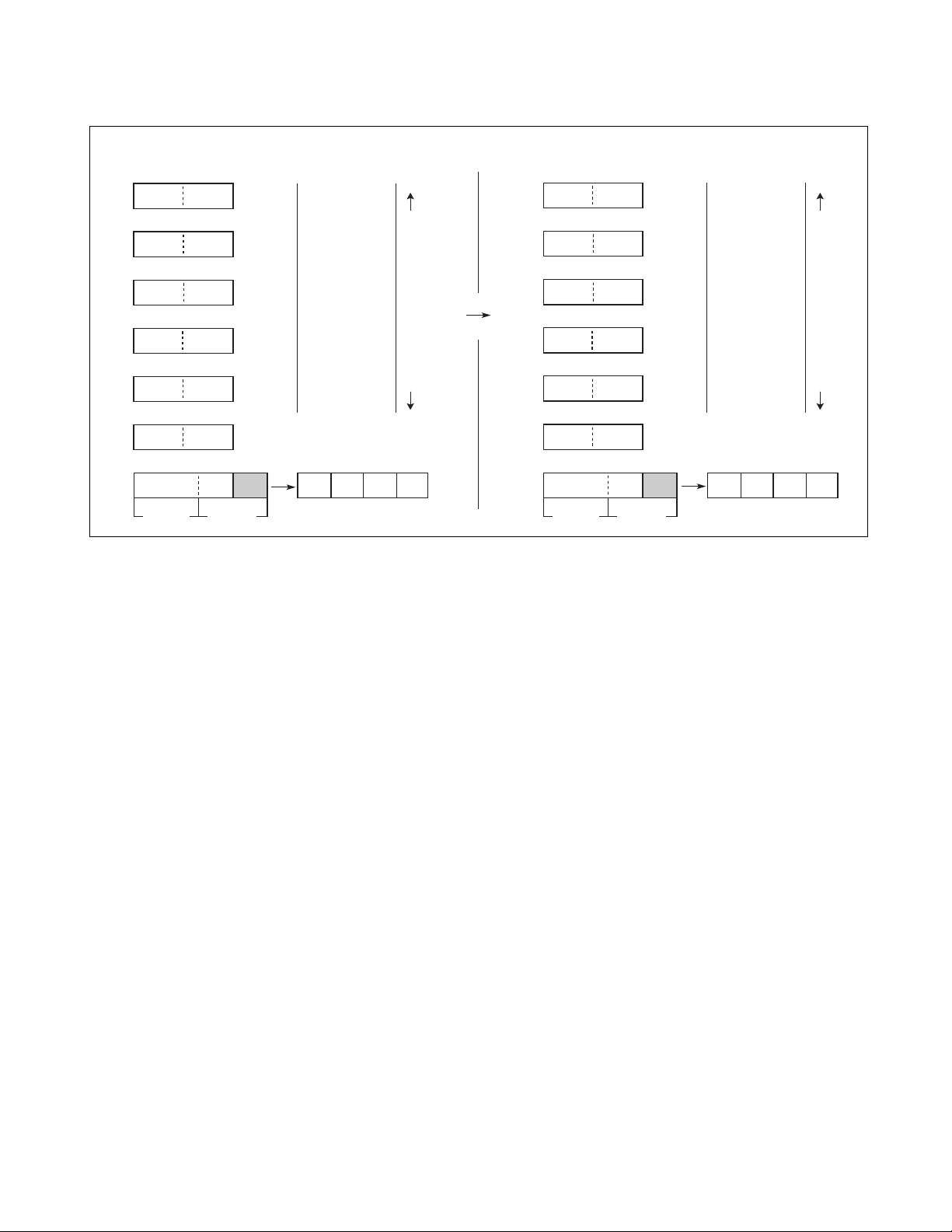
Execution example : ADDC A
CHAPTER 6 DETAILED RULES FOR EXECUTION INSTRUCTIONS
A
T
IX
SP
PC
EP
PS
12 34
56 78
Byte Byte
Memory FFFF
H
A
T
12 AC
56 78
Memory FFFF
IX
SP
PC
Byte
0000
H
EP
NZVC
0000
(Before execution) (After execution)
PS
Byte Byte
Byte
NZVC
1010
0000
H
H
49
Page 62
CHAPTER 6 DETAILED RULES FOR EXECUTION INSTRUCTIONS
6.2 ADDC (ADD Byte Data of Accumulator and Memory with Carry to Accumulator)
Add the byte data of EA memory (memory expressed in each type of addressing) to that
of AL, add a carry to the LSB and then return the results to AL. The contents of AH are
not changed.
■ ADDC (ADD Byte Data of Accumulator and Memory with Carry to Accumulator)
Operation
(AL) ← (AL) + (EA) + (C) (Byte addition with carry)
Assembler format
ADDC A, EA
Condition code (CCR)
NZVC
++++
+: Changed by executing instruction
-: Not changed
N: Set to 1 if the MSB of AL is 1 as the result of operation and set to 0 in other cases.
Z: Set to 1 if the result of operation is 00
V: Set to 1 if an overflow occurs as the result of operation and set to 0 in other cases.
C: Set to 1 if a carry occurs as the result of operation and set to 0 in other cases.
Table 6.2-1 Number of Execution Cycles / Byte Count / OP Code
EA #d8 dir @IX+off @EP Ri
Number of execution
cycles
Byte count 2 2 2 1 1
OP code 24 25 26 27 28 to 2F
and set to 0 in other cases.
H
23 3 2 2
50
Page 63
CHAPTER 6 DETAILED RULES FOR EXECUTION INSTRUCTIONS
Execution example : ADDC A, #25H
A
T
IX
SP
PC
EP
PS
12 34
Byte Byte
Memory FFFF
H Memory FFFFH
12 5A
A
T
IX
SP
PC
Byte Byte
0000H 0000H
EP
NZVC
0100
(Before execution) (After execution)
PS
Byte Byte
NZVC
0000
51
Page 64

CHAPTER 6 DETAILED RULES FOR EXECUTION INSTRUCTIONS
6.3 ADDCW (ADD Word Data of Accumulator and Temporary Accumulator with Carry to Accumulator)
Add the word data of T to that of A, add a carry to the LSB and then return the results to
A.
■ ADDCW (ADD Word Data of Accumulator and Temporary Accumulator with Carry to
Accumulator)
Operation
(A) ← (A) + (T) + (C) (Word addition with carry)
Assembler format
ADDCW A
Condition code (CCR)
NZVC
++++
+: Changed by executing instruction
-: Not changed
N: Set to 1 if the MSB of A is 1 as the result of operation and set to 0 in other cases.
Z: Set to 1 if the result of operation is 0000
V: Set to 1 if an overflow occurs as the result of operation and set to 0 in other cases.
C: Set to 1 if a carry occurs as the result of operation and set to 0 in other cases.
Number of execution cycle: 1
Byte count: 1
OP code: 23
and set to 0 in other cases.
H
52
Page 65

CHAPTER 6 DETAILED RULES FOR EXECUTION INSTRUCTIONS
Execution example : ADDCW A
A
T
IX
SP
PC
EP
PS
12 34
56 78
Byte Byte
Memory FFFF
H Memory FFFFH
68 AD
A
T
56 78
IX
SP
PC
Byte Byte
NZVC
0100
(Before execution) (After execution)
0000H 0000H
EP
NZVC
PS
0000
Byte Byte
53
Page 66

CHAPTER 6 DETAILED RULES FOR EXECUTION INSTRUCTIONS
6.4 AND (AND Byte Data of Accumulator and Temporary Accumulator to Accumulator)
Carry out the logical AND on the byte data of AL and TL for every bit and return the
result to AL. The byte data of AH is not changed.
■ AND (AND Byte Data of Accumulator and Temporary Accumulator to Accumulator)
Operation
(AL) ← (AL) ^ (TL) (Byte AND)
Assembler format
AND A
Condition code (CCR)
NZVC
++R-
+: Changed by executing instruction
-: Not changed
R: Set to 0 by executing instruction
N: Set to 1 if the MSB of AL is 1 as the result of operation and set to 0 in other cases.
Z: Set to 1 if the result of operation is 00
V: Always set to 0
C: Not changed
Number of execution cycle: 1
Byte count: 1
OP code: 62
and set to 0 in other cases.
H
54
Page 67

Execution example : AND A
CHAPTER 6 DETAILED RULES FOR EXECUTION INSTRUCTIONS
A
T
IX
SP
PC
EP
PS
12 34
XX 2C
Byte Byte
Memory FFFF
H Memory FFFFH
12 24
A
T
XX 2C
IX
SP
PC
Byte Byte
NZVC
0000
(Before execution) (After execution)
0000H 0000H
EP
NZVC
PS
0000
Byte Byte
55
Page 68

CHAPTER 6 DETAILED RULES FOR EXECUTION INSTRUCTIONS
6.5 AND (AND Byte Data of Accumulator and Memory to Accumulator)
Carry out the logical AND on the byte data of AL and EA memory (memory expressed in
each type of addressing) for every bit and return the result to AL. The byte data of AH is
not changed.
■ AND (AND Byte Data of Accumulator and Memory to Accumulator)
Operation
(AL) ← (AL) ^ (EA) (Byte AND)
Assembler format
AND A, EA
Condition code (CCR)
NZVC
++R-
+: Changed by executing instruction
-: Not changed
R: Set to 0 by executing instruction
N: Set to 1 if the MSB of AL is 1 as the result of operation and set to 0 in other cases.
Z: Set to 1 if the result of operation is 00
V: Always set to 0
C: Not changed
Table 6.5-1 Number of Execution Cycles / Byte Count / OP Code
EA #d8 dir @IX+off @EP Ri
Number of execution
cycles
Byte count 2 2 2 1 1
OP code 64 65 66 67 68 to 6F
23 3 2 2
and set to 0 in other cases.
H
56
Page 69

CHAPTER 6 DETAILED RULES FOR EXECUTION INSTRUCTIONS
Execution example : AND , @EP
A
T
IX
Memory FFFF
02 53
H Memory FFFFH
A
T
IX
31 0123H
SP
PC
EP
01 23 01 23
Byte Byte
0000H 0000H
SP
PC
EP
NZVC
PS
Byte Byte
0010
(Before execution) (After execution)
PS
02 11
31 0123H
NZVC
0000
Byte Byte
57
Page 70

CHAPTER 6 DETAILED RULES FOR EXECUTION INSTRUCTIONS
6.6 ANDW (AND Word Data of Accumulator and Temporary Accumulator to Accumulator)
Carry out the logical AND on the word data of A and T for every bit and return the
results to A.
■ ANDW (AND Word Data of Accumulator and Temporary Accumulator to Accumulator)
Operation
(A) ← (A) ^ (T) (Word AND)
Assembler format
ANDW A
Condition code (CCR)
NZVC
++R-
+: Changed by executing instruction
-: Not changed
R: Set to 0 by executing instruction
N: Set to 1 if the MSB of A is 1 as the result of operation and set to 0 in other cases.
Z: Set to 1 if the result of operation is 0000
V: Always set to 0
C: Not changed
Number of execution cycle: 1
Byte count: 1
OP code: 63
and set to 0 in other cases.
H
58
Page 71

CHAPTER 6 DETAILED RULES FOR EXECUTION INSTRUCTIONS
Execution example : ANDW A
A
T
IX
SP
PC
EP
PS
56 63
34 32
Byte Byte
Memory FFFF
H Memory FFFFH
14 22
A
T
34 32
IX
SP
PC
Byte Byte
NZVC
0000
(Before execution) (After execution)
0000H 0000H
EP
NZVC
PS
0000
Byte Byte
59
Page 72

CHAPTER 6 DETAILED RULES FOR EXECUTION INSTRUCTIONS
6.7 BBC (Branch if Bit is Clear)
Branch when the value of bit b in dir memory is 0. Branch address corresponds to the
value of addition between the PC value (word value) of the next instruction and the
value with rel code-extended (w ord value).
■ BBC (Branch if Bit is Clear)
Operation
(bit)b = 0: (PC) ← (PC) + 3 + rel (Word addition)
(bit)b = 1: (PC) ← (PC) + 3 (Word addition)
Assembler format
BBC dir:b, rel
Condition code (CCR)
NZVC
-+--
+: Changed by executing instruction
-: Not changed
N: Not changed
Z: Set to 1 when the value of dir:b is 0 and set to 0 when it is 1.
V: Not changed
C: Not changed
Number of execution cycles: 5
Byte count: 3
OP code: B0 to B7
60
Page 73

CHAPTER 6 DETAILED RULES FOR EXECUTION INSTRUCTIONS
Execution example : BBC 84H : 0, 0FBH
Memory FFFF
A
H Memory FFFFH
A
B0 E800H
T
IX
SP
T
IX
SP
bit0
PC
E8 00 E7 FE
XXXX XXX0 0084H
Byte Byte
0000H 0000H
EP
PC
EP
NZVC
PS
00
Byte Byte
0000
(Before execution) (After execution)
PS
00
Byte Byte
B0 E800H
E7FEH
bit0
XXXX XXX0 0084H
NZVC
0001
61
Page 74

CHAPTER 6 DETAILED RULES FOR EXECUTION INSTRUCTIONS
6.8 BBS (Branch if Bit is Set)
Branch when the value of bit b in dir memory is 1. Branch address corresponds to the
value of addition between the PC value (word value) of the next instruction and the
value with rel code-extended (w ord value).
■ BBS (Branch if Bit is Set)
Operation
(bit)b = 0: (PC) ← (PC) + 3 (Word addition)
(bit)b = 1: (PC) ← (PC) + 3 + rel (Word addition)
Assembler format
BBS dir:b, rel
Condition code (CCR)
NZVC
-+--
+: Changed by executing instruction
-: Not changed
N: Not changed
Z: Set to 1 when the value of dir:b is 0 and set to 0 when it is 1.
V: Not changed
C: Not changed
Number of execution cycles: 5
Byte count: 3
OP code: B8 to BF
62
Page 75
CHAPTER 6 DETAILED RULES FOR EXECUTION INSTRUCTIONS
Execution example : BBS 84H : 0, 0FBH
Memory FFFF
A
H Memory FFFFH
A
B0 E800H
T
IX
SP
T
IX
SP
bit0
0084
PC
E8 00 E7 FE
EP
XXXX XXX1
Byte Byte
H
0000H 0000H
PC
EP
NZVC
PS
00
Byte Byte
0000
(Before execution) (After execution)
PS
00
Byte Byte
B0 E800H
E7FEH
bit0
XXXX XXX1
0084
NZVC
0000
H
63
Page 76

CHAPTER 6 DETAILED RULES FOR EXECUTION INSTRUCTIONS
6.9 BC (Branch relative if C=1)/BLO (Branch if LOwer)
Execute the next instruction if the C-flag is 0 and the branch if it is 1. Branch address
corresponds to the value of addition between the PC value (word value) of the next
instruction and the value with rel code-extended (word value).
■ BC (Branch relative if C=1)/BLO (Branch if LOwer)
Operation
(C) = 0: (PC) ← (PC) + 2 (Word addition)
(C) = 1: (PC) ← (PC) + 2 + rel (Word addition)
Assembler format
BC rel/BLO rel
Condition code (CCR)
NZVC
----
+: Changed by executing instruction
-: Not changed
N: Not changed
Z: Not changed
V: Not changed
C: Not changed
Number of execution cycles: 4 (at divergence)/ 2 (at non-divergence)
Byte count: 2
OP code: F9
64
Page 77
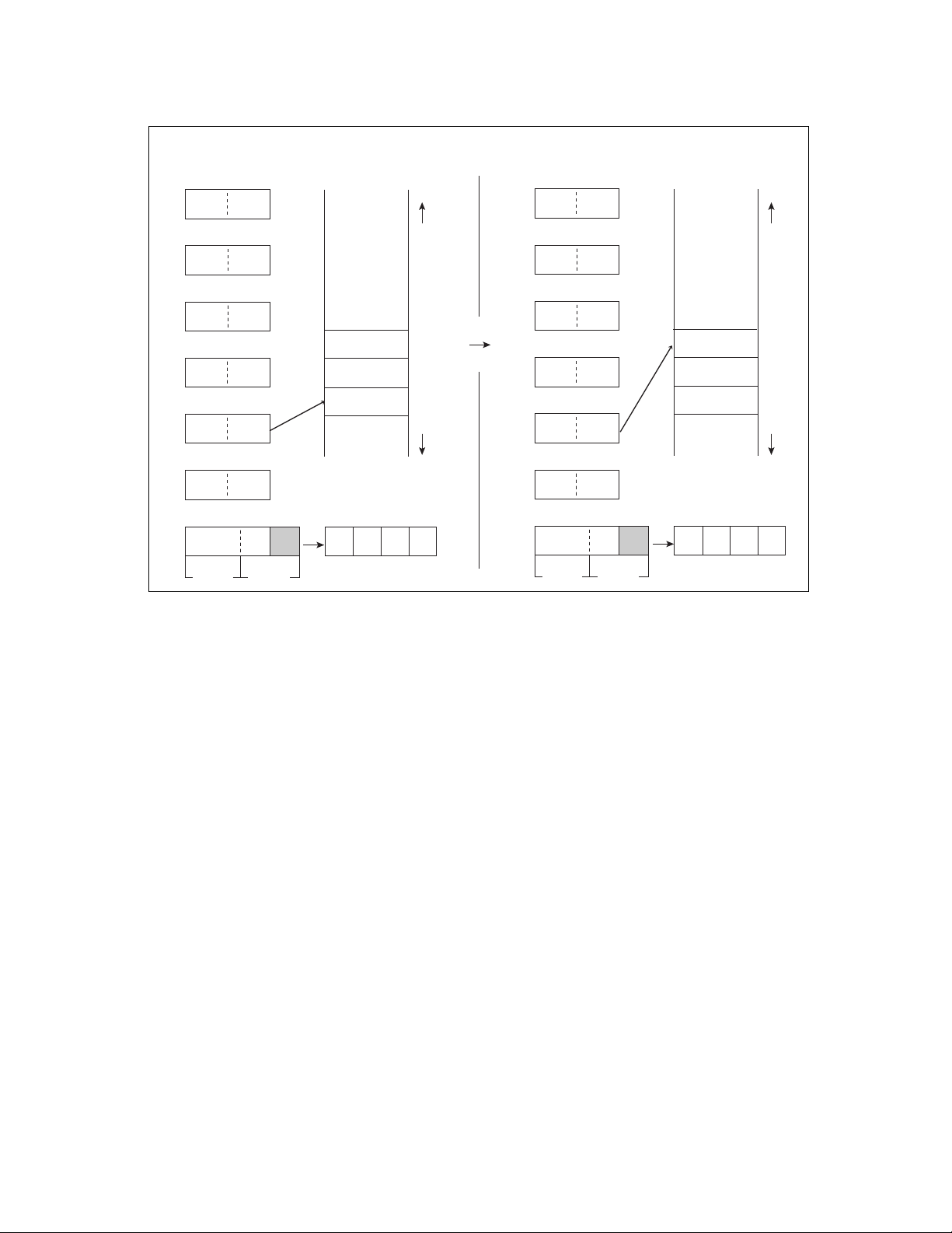
CHAPTER 6 DETAILED RULES FOR EXECUTION INSTRUCTIONS
Execution example : BC 0FEH
Memory FFFF
A
T
IX
SP
FE
F9
PC
E8 02 E8 04
EP
Byte Byte
H Memory FFFFH
A
T
IX
SP
F802H
PC
0000H 0000H
EP
NZVC
PS
Byte Byte
1011
(Before execution) (After execution)
PS
Byte Byte
E804
FE
F9
E802H
NZVC
1011
H
65
Page 78

CHAPTER 6 DETAILED RULES FOR EXECUTION INSTRUCTIONS
6.10 BGE (Branch Great or Equal: relative if larger than or equal to Zero)
Execute the next instruction if the logical exc l usive-OR f or the V and N flags is 1 and the
branch if it is 0. Branch address corresponds to the value of addition between the PC
value (word value) of the next instruction and the value with rel code-extended (word
value).
■ BGE (Branch Great or Equal: relative if larger than or equal to Zero)
Operation
(V) ∀ (N) = 1: (PC) ← (PC) + 2 (Word addition)
(V) ∀ (N) = 0: (PC) ← (PC) + 2 + rel (Word addition)
Assembler format
BGE rel
Condition code (CCR)
NZVC
----
+: Changed by executing instruction
-: Not changed
N: Not changed
Z: Not changed
V: Not changed
C: Not changed
Number of execution cycles: 4 (at divergence)/ 2 (at non-divergence)
Byte count: 2
OP code: FE
66
Page 79
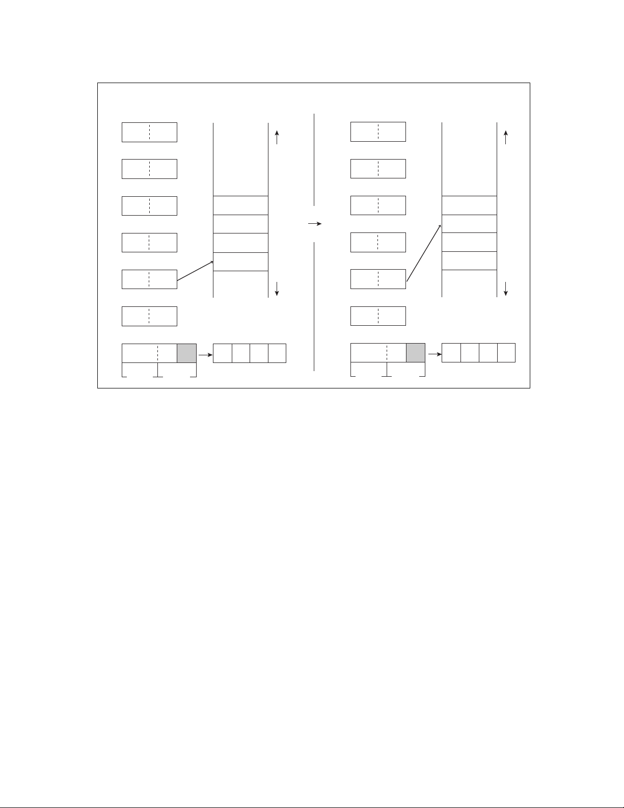
Execution example : BGE 02H
CHAPTER 6 DETAILED RULES FOR EXECUTION INSTRUCTIONS
A
T
IX
SP
Memory FFFF
02
H Memory FFFFH
A
T
IX
SP
F456H F456HFE
PC
F4 56 F4 58
Byte Byte
0000H 0000H
EP
PC
EP
NZVC
PS
Byte Byte
0111
(Before execution) (After execution)
PS
Byte Byte
F458
02
FE
NZVC
0111
H
67
Page 80

CHAPTER 6 DETAILED RULES FOR EXECUTION INSTRUCTIONS
6.11 BLT (Branch Less Than zero: relative if < Zero)
Execute the next instruction if the logical exc l usive-OR f or the V and N flags is 0 and the
branch if it is 1. Branch address corresponds to the value of addition between the PC
value (word value) of the next instruction and the value with rel code-extended (word
value).
■ BLT (Branch Less Than zero: relative if < Zero)
Operation
(V) ∀ (N) = 0: (PC) ← (PC) + 2 (Word addition)
(V) ∀ (N) = 1: (PC) ← (PC) + 2 + rel (Word addition)
Assembler format
BLT rel
Condition code (CCR)
NZVC
----
+: Changed by executing instruction
-: Not changed
N: Not changed
Z: Not changed
V: Not changed
C: Not changed
Number of execution cycles: 4 (at divergence)/ 2 (at non-divergence)
Byte count: 2
OP code: FF
68
Page 81

Execution example : BLT 02H
CHAPTER 6 DETAILED RULES FOR EXECUTION INSTRUCTIONS
Memory FFFF
A
T
IX
H Memory FFFFH
A
T
IX
F458H F458H
SP
02
SP
F456H F456HFF
PC
F4 56 F4 5A
EP
Byte Byte
0000H 0000H
PC
EP
NZVC
PS
Byte Byte
0111
(Before execution) (After execution)
PS
Byte Byte
F45A
02
FF
NZVC
0111
H
69
Page 82

CHAPTER 6 DETAILED RULES FOR EXECUTION INSTRUCTIONS
6.12 BN (Branch relative if N = 1)
Execute the next instruction if the N-flag is 0 and the branch if it is 1. Branch address
corresponds to the value of addition between the PC value (word value) of the next
instruction and the value with rel code-extended (word value).
■ BN (Branch relative if N = 1)
Operation
N = 0: (PC) ← (PC) + 2 (Word addition)
N = 1: (PC) ← (PC) + 2 + rel (Word addition)
Assembler format
BN rel
Condition code (CCR)
NZVC
----
+: Changed by executing instruction
-: Not changed
N: Not changed
Z: Not changed
V: Not changed
C: Not changed
Number of execution cycles: 4 (at divergence)/ 2 (at non-divergence)
Byte count: 2
OP code: FB
70
Page 83

Execution example : BN 02H
CHAPTER 6 DETAILED RULES FOR EXECUTION INSTRUCTIONS
Memory FFFF
A
T
IX
SP
H Memory FFFFH
A
T
IX
SP
02
PC
FC 5F FC 63
EP
FB
Byte Byte
FC5F
H FC5FH
0000H 0000H
PC
EP
NZVC
PS
Byte Byte
1011
(Before execution) (After execution)
PS
Byte Byte
FC63
02
FB
NZVC
1011
H
71
Page 84

CHAPTER 6 DETAILED RULES FOR EXECUTION INSTRUCTIONS
6.13 BNZ (Branch relative if Z = 0)/BNE (Branch if Not Equal)
Execute the next instruction if the Z-flag is 1 and the branch if it is 0. Branch address
corresponds to the value of addition between the PC value (word value) of the next
instruction and the value with rel code-extended (word value).
■ BNZ (Branch relative if Z = 0)/BNE (Branch if Not Equal)
Operation
(Z) = 1: (PC) ← (PC) + 2 (Word addition)
(Z) = 0: (PC) ← (PC) + 2 + rel (Word addition)
Assembler format
BNZ rel/BNE rel
Condition code (CCR)
NZVC
----
+: Changed by executing instruction
-: Not changed
N: Not changed
Z: Not changed
V: Not changed
C: Not changed
Number of execution cycles: 4 (at divergence)/ 2 (at non-divergence)
Byte count: 2
OP code: FC
72
Page 85

Execution example : BNZ 0FAH
A
CHAPTER 6 DETAILED RULES FOR EXECUTION INSTRUCTIONS
Memory FFFF
H Memory FFFFH
A
T
IX
SP
FA
T
IX
SP
FE1EH FE1EHFC
PC
FE 1E FE 20
Byte Byte
0000H 0000H
EP
PC
EP
NZVC
PS
Byte Byte
0001
(Before execution) (After execution)
PS
Byte Byte
FE20
FA
FC
NZVC
0001
H
73
Page 86

CHAPTER 6 DETAILED RULES FOR EXECUTION INSTRUCTIONS
6.14 BNC (Branch relative if C = 0)/BHS (Branch if Higher or Same)
Execute the next instruction if the C-flag is 1 and the branch if it is 0 . Branch address
corresponds to the value of addition between the PC value (word value) of the next
instruction and the value with rel code-extended (word value).
■ BNC (Branch relative if C = 0)/BHS (Branch if Higher or Same)
Operation
(C) = 1: (PC) ← (PC) + 2 (Word addition)
(C) = 0: (PC) ← (PC) + 2 + rel (Word addition)
Assembler format
BNC rel/BHS rel
Condition code (CCR)
NZVC
----
+: Changed by executing instruction
-: Not changed
N: Not changed
Z: Not changed
V: Not changed
C: Not changed
Number of execution cycles: 4 (at divergence)/ 2 (at non-divergence)
Byte count: 2
OP code: F8
74
Page 87

Execution example : BNC 01H
CHAPTER 6 DETAILED RULES FOR EXECUTION INSTRUCTIONS
Memory FFFF
A
T
IX
H Memory FFFFH
A
T
IX
E804H
SP
01
SP
E802H E802HF8
PC
E8 02 E8 05
Byte Byte
0000H 0000H
EP
PC
EP
NZVC
PS
Byte Byte
1011
(Before execution) (After execution)
PS
Byte Byte
E805
E804H
01
F8
NZVC
1011
H
75
Page 88

CHAPTER 6 DETAILED RULES FOR EXECUTION INSTRUCTIONS
6.15 BP (Branch relative if N = 0: PLUS)
Execute the next instruction if the N-flag is 1 and the branch if it is 0 . Branch address
corresponds to the value of addition between the PC value (word value) of the next
instruction and the value with rel code-extended (word value).
■ BP (Branch relative if N = 0: PLUS)
Operation
(N) = 1: (PC) ← (PC) + 2 (Word addition)
(N) = 1: (PC) ← (PC) + 2 + rel (Word addition)
Assembler format
BP rel
Condition code (CCR)
NZVC
----
+: Changed by executing instruction
-: Not changed
N: Not changed
Z: Not changed
V: Not changed
C: Not changed
Number of execution cycles: 4 (at divergence)/ 2 (at non-divergence)
Byte count: 2
OP code: FA
76
Page 89

Execution example : BP 04H
CHAPTER 6 DETAILED RULES FOR EXECUTION INSTRUCTIONS
A
T
IX
SP
Memory FFFF
04
H Memory FFFFH
A
T
IX
SP
FC5FH FC5FHFA
PC
FC 5F FC 61
EP
Byte Byte
0000H 0000H
PC
EP
NZVC
PS
Byte Byte
1110
(Before execution) (After execution)
PS
Byte Byte
FC61
04
FA
NZVC
1110
H
77
Page 90

CHAPTER 6 DETAILED RULES FOR EXECUTION INSTRUCTIONS
6.16 BZ (Branch relative if Z = 1)/BEQ (Branch if Equal)
Execute the next instruction if the Z-flag is 0 and the branch if it is 1 . Branch address
corresponds to the value of addition between the PC value (word value) of the next
instruction and the value with rel code-extended (word value).
■ BZ (Branch relative if Z = 1)/BEQ (Branch if Equal)
Operation
(Z) = 0: (PC) ← (PC) + 2 (Word addition)
(Z) = 1: (PC) ← (PC) + 2 + rel (Word addition)
Assembler format
BZ rel/BEQ rel
Condition code (CCR)
NZVC
----
+: Changed by executing instruction
-: Not changed
N: Not changed
Z: Not changed
V: Not changed
C: Not changed
Number of execution cycles: 4 (at divergence)/ 2 (at non-divergence)
Byte count: 2
OP code: FD
78
Page 91
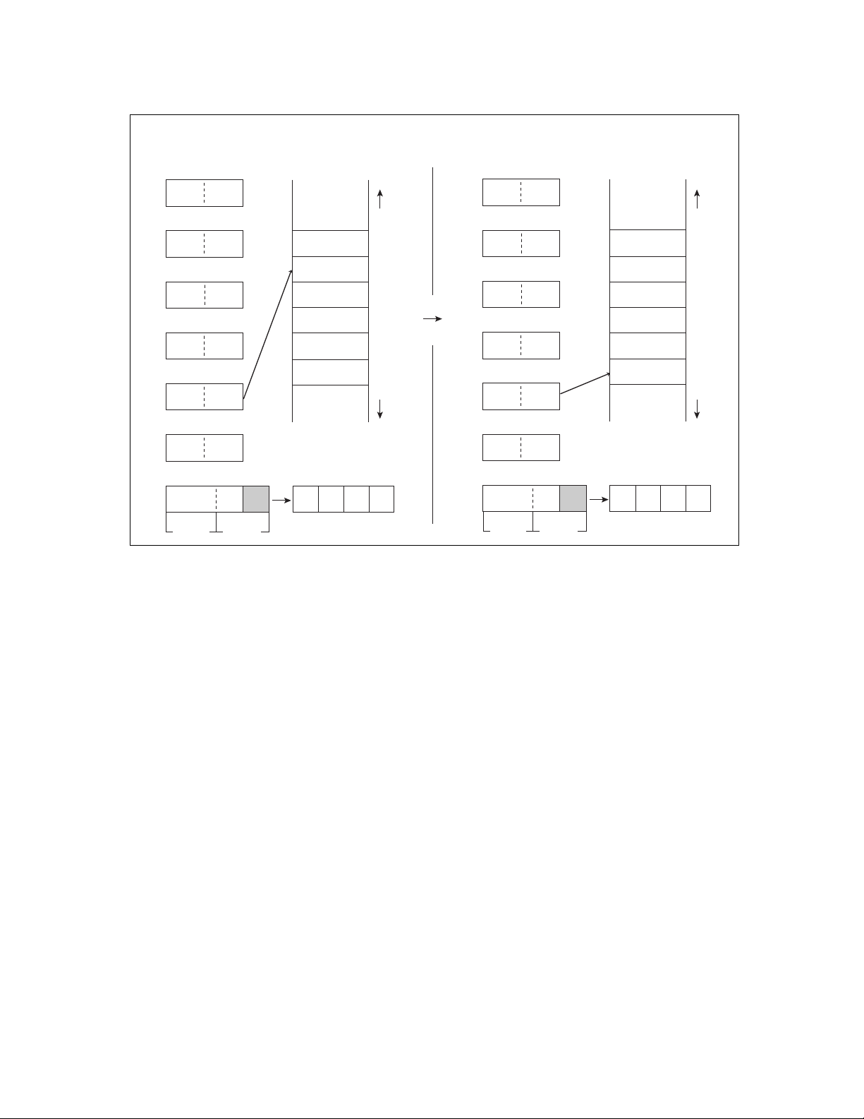
Execution example : BZ 0FAH
CHAPTER 6 DETAILED RULES FOR EXECUTION INSTRUCTIONS
Memory FFFF
A
H Memory FFFFH
A
FE20H
T
FA
FD
FE1EH
IX
SP
PC
FE 1E FE 1A
Byte Byte
0000H 0000H
EP
T
IX
SP
PC
EP
NZVC
PS
Byte Byte
0001
(Before execution) (After execution)
PS
Byte Byte
FA
FD
FE1EH
FE1AH
NZVC
0001
79
Page 92

CHAPTER 6 DETAILED RULES FOR EXECUTION INSTRUCTIONS
6.17 CALL (CALL subroutine)
Branch to address of ext. Return to the instruction next to this one by using the RET
instruction of the branch subroutine.
■ CALL (CALL subroutine)
Operation
(SP) ← (SP) - 2 (Word subtraction), ((SP)) ← (PC) (Word transfer)
(PC) ← ext
Assembler format
CALL ext
Condition code (CCR)
NZVC
----
+: Changed by executing instruction
-: Not changed
N: Not changed
Z: Not changed
V: Not changed
C: Not changed
Number of execution cycles: 6
Byte count: 3
OP code: 31
80
Page 93
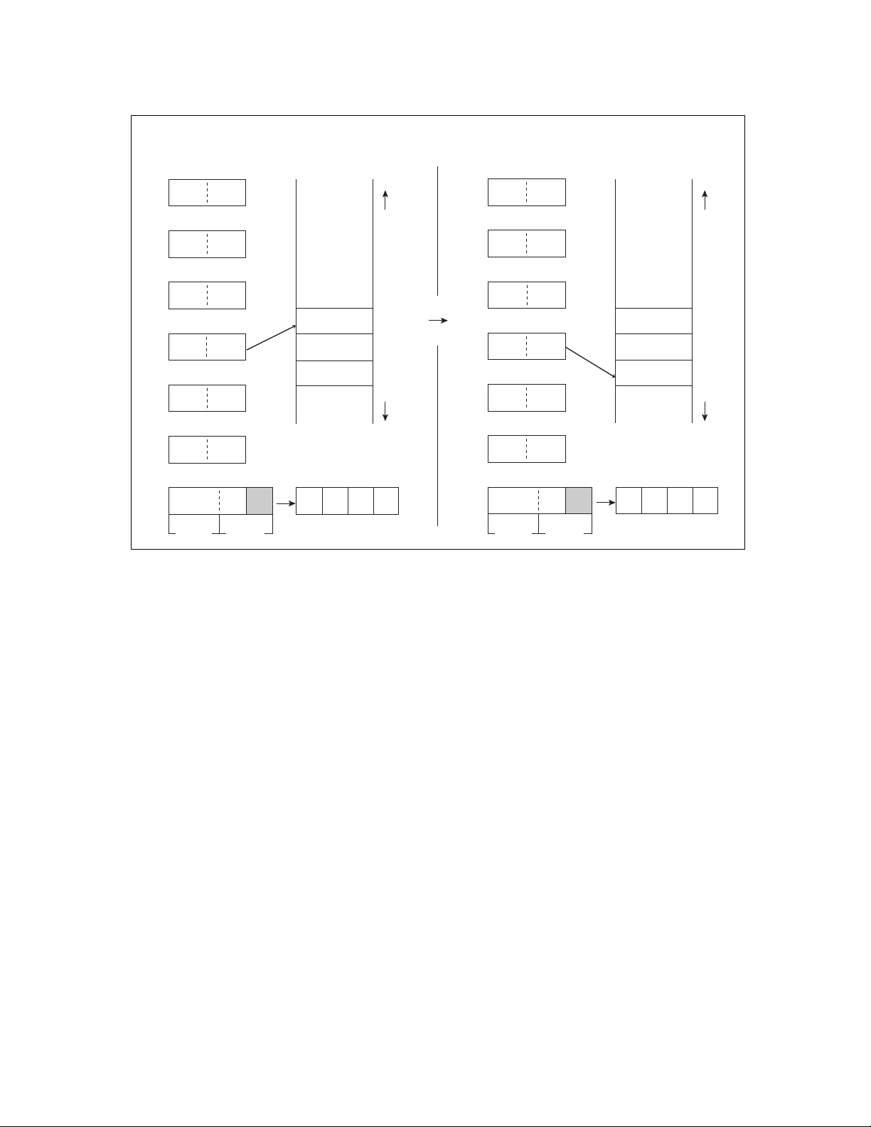
CHAPTER 6 DETAILED RULES FOR EXECUTION INSTRUCTIONS
Execution example : CALL 0FC00H
Memory FFFF
A
T
IX
H Memory FFFFH
A
T
IX
020AH
SP
02 OA 02 08
PC
F6 23 FC 00
Byte Byte
0000H 0000H
EP
SP
PC
EP
NZVC
PS
Byte Byte
0000
(Before execution) (After execution)
PS
Byte Byte
020AH
26
F6
0208H
NZVC
0000
81
Page 94

CHAPTER 6 DETAILED RULES FOR EXECUTION INSTRUCTIONS
6.18 CALLV (CALL Vectored subroutine)
Branch to the vector address (VA) of vct. Return to the instruction next to this one by
using the RET instruction of the branch subroutine. The vector address (VA) indicated
by VCT is shown on the next page.
■ CALLV (CALL Vectored subroutine)
Operation
(SP) ← (SP) - 2 (Word subtraction), ((SP)) ← (PC) (Word transfer)
(PC) ← (VA)
Assembler format
CALLV #vct
Condition code (CCR)
NZVC
----
+: Changed by executing instruction
-: Not changed
N: Not changed
Z: Not changed
V: Not changed
C: Not changed
Number of execution cycles: 7
Byte count: 1
OP code: E8 to EF
82
Page 95
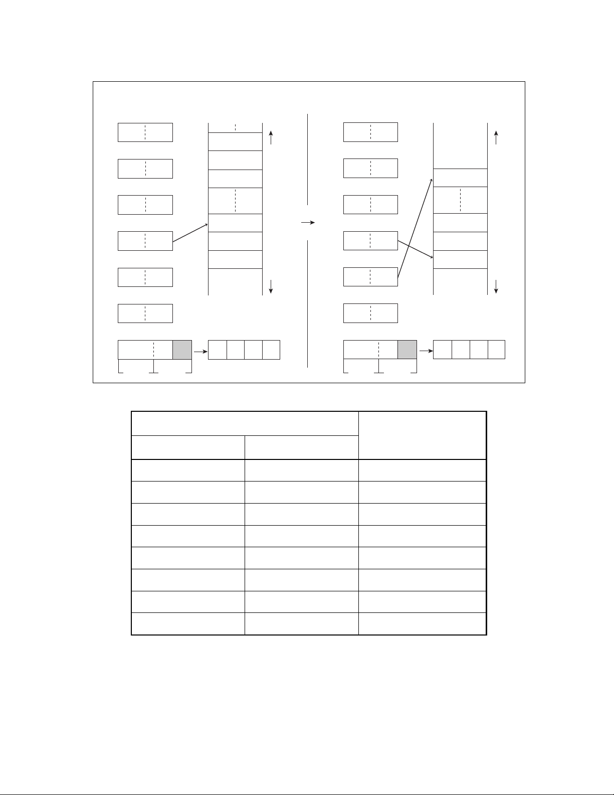
CHAPTER 6 DETAILED RULES FOR EXECUTION INSTRUCTIONS
Execution example : CALL #02H
A
T
IX
SP
PC
EP
PS
02 08
E8 00
Byte Byte
Memory FFFF
vct
02
NZVC
0000
(Before execution) (After execution)
00
EC
Byte Byte
H Memory FFFFH
A
H
FFC5
T
FFC4H
IX
0208H
SP
02 06
PC
EC 00
0000H 0000H
EP
PS
Byte Byte
Table 6.18-1 Call Storage Address of Vector Call Instruction
EC00H
0208H
01
E8
NZVC
0000
0206H
Vector address (VA)
Lower address Upper address
FFCE
FFCC
FFCA
FFC8
FFC6
FFC4
FFC2
FFC0
H
H
H
H
H
H
H
H
FFCF
FFCD
FFCB
FFC9
FFC7
FFC5
FFC3
FFC1
H
H
H
H
H
H
H
H
Instruction
CALL#7
CALL#6
CALL#5
CALL#4
CALL#3
CALL#2
CALL#1
CALL#0
83
Page 96

CHAPTER 6 DETAILED RULES FOR EXECUTION INSTRUCTIONS
6.19 CLRB (Clear direct Memory Bit)
Set the contents of 1 bit (indicated by 3 lower bits (b) of mnemonic) of the direct area to
0.
■ CLRB (Clear direct Memory Bit)
Operation
(dir:b) ← 0
Assembler format
CLRB dir:b
Condition code (CCR)
NZVC
----
+: Changed by executing instruction
-: Not changed
N: Not changed
Z: Not changed
V: Not changed
C: Not changed
Number of execution cycles: 4
Byte count: 2
OP code: A0 to A7
84
Page 97

CHAPTER 6 DETAILED RULES FOR EXECUTION INSTRUCTIONS
Execution example : CLRB 84H : 0
A
T
IX
SP
PC
EP
PS
Memory FFFF
H Memory FFFFH
A
T
IX
SP
0084H0000 000X
PC
Byte Byte
0000H 0000H
EP
NZVC
00 00
Byte Byte
0000
(Before execution) (After execution)
PS
Byte Byte
0084
NZVC
0000
H0000 0000
85
Page 98

CHAPTER 6 DETAILED RULES FOR EXECUTION INSTRUCTIONS
6.20 CLRC (Clear Carry flag)
Set the C-flag to 0.
■ CLRC (Clear Carry flag)
Operation
(C) ← 0
Assembler format
CLRC
Condition code (CCR)
NZVC
---R
+: Changed by executing instruction
-: Not changed
R: Set to 0 by executing instruction
N: Not changed
Z: Not changed
V: Not changed
C: Set to 0.
Number of execution cycle: 1
Byte count: 1
OP code: 81
86
Page 99

Execution example : CLRC
CHAPTER 6 DETAILED RULES FOR EXECUTION INSTRUCTIONS
A
T
IX
SP
PC
EP
PS
Byte Byte
Memory FFFF
H Memory FFFFH
A
T
IX
SP
PC
Byte Byte
NZVC
0100
(Before execution) (After execution)
0000H 0000H
EP
NZVC
PS
0000
Byte Byte
87
Page 100

CHAPTER 6 DETAILED RULES FOR EXECUTION INSTRUCTIONS
6.21 CLRI (CLeaR Interrupt flag)
Set the I-flag to 0.
■ CLRI (CLeaR Interrupt flag)
Operation
(I) ← 0
Assembler format
CLRI
Condition code (CCR)
INZVC
R----
+: Changed by executing instruction
-: Not changed
R: Set to 0 by executing instruction
I: Set to 0
N: Not changed
Z: Not changed
V: Not changed
C: Not changed
Number of execution cycle: 1
Byte count: 1
OP code: 80
88
 Loading...