

Page 1
查询MB90520A供应商
FUJITSU SEMICONDUCTOR
DATA SHEET
DS07-13707-3E
16-bit Proprietary Microcontroller
CMOS
F2MC-16LX MB90520A/520B Series
MB90522A/523A/522B/523B/F523B/V520A
DESCRIPTION
■
The MB90520A/520B series is a general-purpose 16-bit microcontroller designed for process control applications
in consumer products that require high-speed real-time processing.
The microcontroller instruction set is based on the AT architecture of the F
for high-level languages, extended addressing modes, enhanced multiplication and division instructions, and a
complete range of bit manipulation instructions. The microcontroller has a 32-bit accumulator for processing long
word (32-bit) data.
The MB90520A/520B series peripheral resources include an 8/10-bit A/D converter, 8-bit D/A converter, UART
(SCI) , extended I/O serial interfaces 0 and 1, 8/16-bit up/do wn counter/timers 0 and 1, 8/16-bit PPG timers 0 and
1, a range of I/O timers (16-bit free-run timers 1 and 2, input capture (ICU) 0 and 1, and output compare (OCU)
0 and 1) , an LCD controller/driver, 8 external interrupt inputs, and 8 wakeup interrupts.
2
* : F
MC stands for FUJITSU Flexible MicroController, a registered trademark of FUJITSU LIMITED.
FEATURES
■
•Clock
• Internal PLL clock multiplication circuit
• Selectable machine clock (PLL clock) : Base oscillation divided by two or multiplied by one to four
(For a 4 MHz base oscillation, the machine clock range is 4 MHz to 16 MHz) .
PACKAGES
■
2
MC* family with additional instructions
(Continued)
120-pin, Plastic, LQFP 120-pin, Plastic, QFP
(FPT-120P-M05) (FPT-120P-M13)
Page 2

MB90520A/520B Series
(Continued)
• Sub-clock (32.768 KHz) operation available
Minimum instruction execution time : 62.5 ns (for oscillation = 4 MHz, PLL clock setting = ×4, VCC = 5.0 V)
•
16MB CPU memory space
Internal 24-bit addressing
•
Instruction set optimized for controller applications
Rich data types (bit, byte, word, long-word)
Extended addressing modes (23 types)
Enhanced signed multiplication and division instructions and RETI instruction
Enhanced calculation precision using a 32-bit accumulator
•
Instruction set designed for high-level language (C) and multi-tasking
System stack pointer
Enhanced pointer-indirect instructions and barrel shift instructions
•
Faster execution speed
4-byte instruction queue
ROM mirror function (48 Kbytes of bank FF is mirrored in bank 00)
•
Program patch function
•
Interrupt function
32 programmable interrupts with 8 levels
•
Automatic data transmission function independent of CPU operation
Extended intelligent I/O service function (EI
•
Low-power consumption (stand-by) modes
Sleep mode (CPU operating clock stops, peripherals continue to operate.)
Pseudo-clock mode (Only oscillation clock and timebase timer continue to operate.)
Clock mode (Main oscillation clock stops, sub-clock and clock timer continue to operate.)
Stop mode (Main oscillation and sub-clock both stop.)
CPU intermittent operation mode
Hardware stand-by mode (Change to stop mpde by operating hardware stand-by pins.)
•
Process
CMOS technology
•I/
O ports
General-purpose I/O ports (CMOS input/output) : 53 ports
General-purpose I/O ports (inputs with pull-up resistors) : 24 ports
General-purpose I/O ports (Nch open-drain outputs) : 8 ports
•
Timers
Timebase timer, clock timer, watchdog timer : 1 channel each
8/16-bit PPG timers 0 and 1 : 8-bit × 2 channels or 16-bit × 1 channel
16-bit reload timers 0 and 1 : 2 channels
16-bit I/O timers :
16-bit free-run timers 0 and 1 : 2 channels
16-bit input capture 0 : 2 channels (2 channels per unit)
16-bit output compare 0 and 1 : 8 channels (4 channels per unit)
8/16-bit up/down counter/timers 0 and 1 : 8-bit × 2 channels or 16-bit × 1 channel
Clock output function : 1 channel
•
Communications macro (communication interface
Extended I/O serial interfaces 0 and 1 : 2 channels
UART (full-duplex, double-buffered, SCI : Can also be used for synchronous serial transfer) : 1 channel
:
An address match detection function (2
2
OS) : Up to 16 channels
)
×
addresses
)
2
Page 3

MB90520A/520B Series
•
External event interrupt control function
DTP/external interrupts : 8 channels (Can be set to detect rising edges, falling edges, “H” levels, or “L” le v els)
Wake-up interrupts : 8 channels (Detects “L” levels only)
Delayed interrupt generation module : 1 channel (for task switching)
•
Analog/digital conversion
8/10-bit A/D converter : 8 channels (Can be initiated by an external trigger. Minimum conversion time = 10.2
µs for a 16 MHz machine clock)
8-bit D/A converter : 2 channels (R-2R type. Settling time = 12.5 µs for a 16 MHz machine clock)
•
Display function
LCD controller/driver : 32 × segment drivers + 4 × common drivers
•
Other
Supports serial writing to flash memory. (Only on versions with on-board flash memory.)
Note : The MB90520A and 520B series cannot be used in external bus mode. Always set these devices to single-
chip mode.
3
Page 4
MB90520A/520B Series
PRODUCT LINEUP
■
Part
Number MB90522A MB90523A MB90522B MB90523B MB90F523B MB90V520A
Parameter
Classification Mask ROM Flash ROM
ROM size 64 Kbytes 128 Kbytes 64 Kbytes 128 Kbytes 128 Kbytes
RAM size 4 Kbytes 6 Kbytes
Separate emulator
power supply
Process CMOS
Operating power
supply voltage
Internal regulator circuit not mounted mounted
CPU functions
Low power operation
(standby modes)
I/O ports
Timebase timer
*1
*2
No
3.0 V to 5.5 V 2.7 V to 5.5 V 3.0 V to 5.5 V
Number of instructions : 340
Instruction sizes : 8-bit, 16-bit
Instruction length : 1 byte to 7 bytes
Data sizes : 1-bit, 8-bit, 16-bit
Minimum instruction execution time : 62.5 ns (for a 16 MHz machine clock)
Interrupt processing time : 1.5 µs min. (for a 16 MHz machine clock)
Sleep mode, clock mode, pseudo-clock mode, stop mode, hardware standby mode,
and CPU intermittent operation mode
General-purpose I/O ports (CMOS outputs) : 53
General-purpose I/O ports (inputs with pull-up resistors) : 24
General-purpose I/O ports (Nch open drain outputs) : 8
Total : 85
18-bit counter
Interrupt interval : 1.024 ms, 4.096 ms, 16.384 ms, 131.072 ms
(for a 4 MHz base oscillation)
Evaluation
product
Watchdog timer
16-bit
I/O
timers
16-bit reload timer
4
16-bit
freerun
timer
16-bit
output
compare
16-bit
input
capture
Reset trigger period
• For a 4 MHz base oscillation : 3.58, 14.33, 57.23, 458.75 ms
• For 32.768 sub-clock operation : 0.438, 3.500, 7.000, 14.000 s
Number of channels : 2
Generates an interrupt on overflow
Number of channels : 8
Pin change timing : Free run timer register value equals output compare register value.
Number of channels : 2
Saves the value of the freerun timer register when a pin input occurs (rising edge, falling
edge, either edge) .
Number of channels : 2
Count clock frequency : 0.125, 0.5, or 2.0 µs for a 16 MHz machine clock
Can be used to count an external event clock.
(Continued)
Page 5
(Continued)
Parameter
MB90520A/520B Series
Part
Number MB90522A MB90523A MB90522B MB90523B MB90F523B MB90V520A
Clock timer
8/16-bit PPG timer
8/16 -bit up/down
counter/timers
15-bit timer
Interrupt interval : 0.438, 0.5, or 2.0 µs for sub-clock frequency = 32.768 kHz
Number of channels : 1 (Can be used in 2 × 8-bit channel mode)
Can generate a pulse waveform output with specified period and 0 to 100% duty ratio.
Number of channels : 1 (Can be used in 2 × 8-bit channel mode)
External event inputs : 6 channels
Reload/compare function : 8-bit × 2 channels
Clock monitor Clock output frequency : Machine clock/2
Delayed interrupt
generation module
Interrupt generation module for task switching. (Used by REALOS.)
Input channels : 8
DTP/External
interrupts
Generates interrupts to the CPU on rising edges, falling edges with input “H” level, or “L”
level.
Can be used for external event interrupts and to activate EI
Wakeup interrupts
Input channels : 8
Triggered by “L” level.
Number of channels : 8
8/10-bit A/D converter
(successive
approximation type)
Resolution : 8-bit or 10-bit selectable
Conversion can be performed sequentially for multiple consecutive channels.
• Single-shot conversion mode : Converts specified channel once only.
• Continuous conversion mode : Repeatedly converts specified channel.
• Intermittent conversion mode : Converts specified channel then halts temporarily.
1
to machine clock/2
2
OS.
8
8-bit D/A converter
(R-2R type)
Number of channels : 2
Resolution : 8-bit
Number of channels : 1
UART (SCI)
Clock synchronous transfer : 62.5 Kbps to 1 Mbps
Clock asynchronous transfer : 1202 bps to 31250 bps
Supports bi-directional and master-slave communications.
Extended I/O serial
interface
Number of channels : 2
Clock synchronous transfer : 31.25 Kbps to 1 Mbps (Using internal shift clock)
Transmission format : Selectable LSB-first or MSB-first
Number of common outputs : 4
Number of segment outputs : 32
LCD controller/driver
Number of power supply pins for LCD drive : 4
LCD display memory : 16 bytes
Divider resistor for LCD drive : Internal
*1 : As for the necessity of a DIP switch setting (S2) when using the emulation pod (MB2145-507) .
Refer to the hardware manual for the emulation pod (MB2145-507) fomr details.
*2 : Take note of the maximum operating frequency and A/D con verter precision restrictions when operating at 3.0 V
to 3.6 V. See the “Electrical Characteristics” section for details.
5
Page 6
MB90520A/520B Series
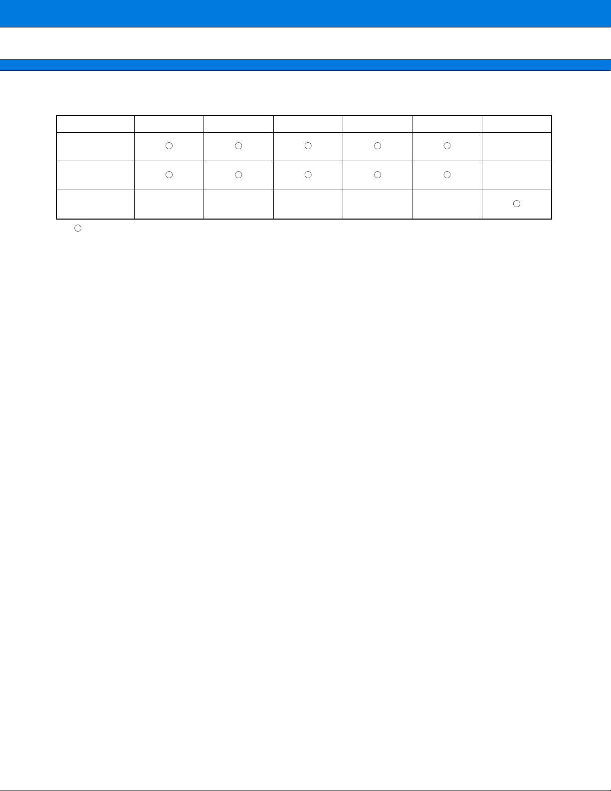
PACKAGES AND CORRESPONDING PRODUCTS
■
Package MB90522A MB90523A MB90522B MB90523B MB90F523B MB90V520A
FPT-120P-M05
(LQFP)
×
FPT-120P-M13
(QFP)
PGA-256C-A01
(PGA)
: Available, : Not available
Note : See the “■ PACKAGE DIMENSIONS” section for more details.
ЧЧЧЧЧ
×
×
6
Page 7
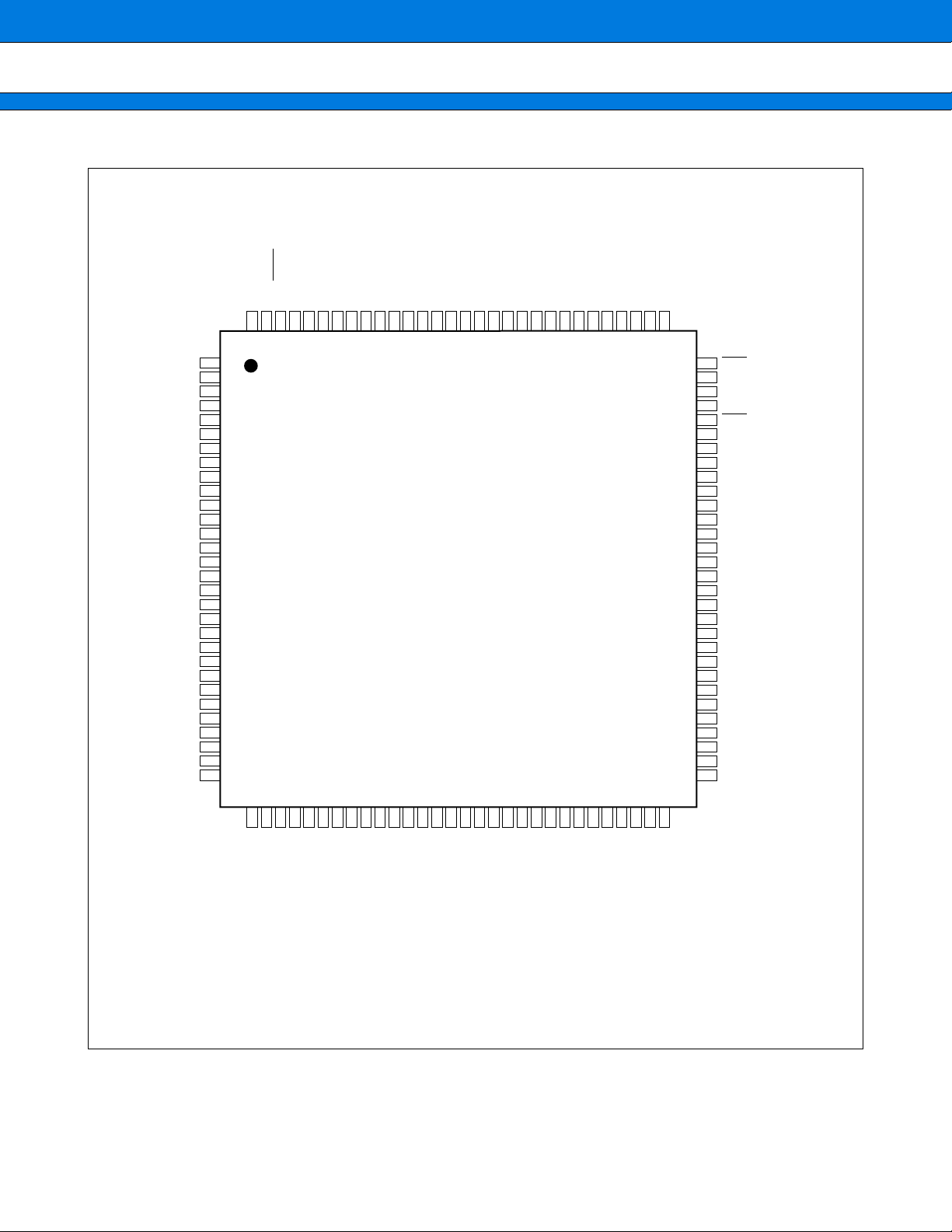
PIN ASSIGNMENT
■
MB90520A/520B Series
(TOP VIEW)
P31/CKOT
P32/OUT0
P33/OUT1
P34/OUT2
P35/OUT3
P36/PG00
P37/PG01
CC
V
P40/PG10
P41/PG11
P42/SIN0
P43/SOT0
P44/SCK0
P45/SIN1
P46/SOT1
P47/SCK1
SEG0
SEG1
SEG2
SEG3
SEG4
SEG5
SEG6
SEG7
PA0/SEG8
PA1/SEG9
PA2/SEG10
PA3/SEG11
PA4/SEG12
PA5/SEG13
P30
VSSP27/ADTG
P26/ZIN0/INT7
P25/BIN0
P24/AIN0
P23/IC11
P22/IC10
P21/IC01
P20/IC00
P17/WI7
P16/WI6
P15/WI5
P14/WI4
P13/WI3
P12/WI2
P11/WI1
P10/WI0
P07
P06/INT6
P05/INT5
P04/INT4
P03/INT3
P02/INT2
P01/INT1
120
119
118
117
116
115
114
113
112
111
110
109
108
107
106
105
104
103
102
101
1
2
3
4
5
6
7
8
9
10
11
12
13
14
15
16
17
18
19
20
21
22
23
24
25
26
27
28
29
30
3132333435363738394041424344454647484950515253545556575859
1009998979695949392
P00/INT0
VCCX1X0V
SS
91
90
89
88
87
86
85
84
83
82
81
80
79
78
77
76
75
74
73
72
71
70
69
68
67
66
65
64
63
62
61
60
RST
MD0
MD1
MD2
HST
V3
V2
V1
V0
P97/SEG31
P96/SEG30
P95/SEG29
P94/SEG28
P93/SEG27
P92/SEG26
P91/SEG25
X0A
X1A
P90/SEG24
P87/SEG23
P86/SEG22
P85/SEG21
P84/SEG20
P83/SEG19
P82/SEG18
P81/SEG17
P80/SEG16
V
SS
P77/COM3
P76/COM2
PA6/SEG14
PA7/SEG15
SS
V
C
P50/SIN2/AIN1
P51/SOT2/BIN1
P52/SCK2/ZIN1
CC
DV
CC
DVSS
AV
AVRL
AVRH
P53/DA0
P54/DA1
(FPT-120P-M05)
(FPT-120P-M13)
SS
AV
P60/AN0
P61/AN1
P62/AN2
P63/AN3
P64/AN4
P65/AN5
P66/AN6
P67/AN7
CC
V
P70/TI0/OUT4
P71/TO0/OUT5
P72/TI1/OUT6
P73/TO1/OUT7
P74/COM0
P75/COM1
7
Page 8
MB90520A/520B Series
PIN DESCRIPTIONS
■
Pin No.
*1
LQFP-120
QFP-120
92, 93 X0, X1 A Oscillator pin
74, 73 X0A, X1A B Sub-oscillator pin
89 to 87
90 RST
86 HST
95 to 101
102 P07 D
103 to 110
111, 112,
113, 114
115
116
117
Pin Name
*2
MD0 to
MD2
P00 to
P06
INT0 to
INT6
P10 to
P17
WI0 to
WI7
P20, P21,
P22, P23
IC00, IC01,
IC10, IC11
P24
AIN0
P25
BIN0
P26
ZIN0
INT7 Event input pin for ch.7 of the DTP/external interrupt circuit
Circuit
Type
Input pins for setting the operation mode.
C
Connect directly to V
C External reset input pin
C Hardware standby input pin
General-purpose I/O ports
The settings in the pull-up resistor setup register (RDR0) are enabled
when ports are set as inputs.
D
The RDR0 settings are ignored when ports are set as outputs.
Event input pins for ch.0 to ch.6 of the DTP/external interrupt circuit
General-purpose I/O port
The settings in the pull-up resistor setup register (RDR0) are enabled when
ports are set as inputs.
The RDR0 settings are ignored when ports are set as outputs.
General-purpose I/O ports
The settings in the pull-up resistor setup register (RDR1) are enabled when
ports are set as inputs.
D
The RDR1 settings are ignored when ports are set as outputs.
Event input pins for the wakeup interrupts.
General-purpose I/O ports
Trigger input pins for input capture units (ICU) 0 and 1.
E
Input operates continuously when channels 0 and 1 of input capture units
(ICU) 0 and 1 are operating. Accordingly, output to the pins from other func-
tions that share this pin must be suspended unless performed intentionally.
General-purpose I/O port
E
Also can be used as the count clock A input to 8/16-bit up/down counter/
timer 0.
General-purpose I/O port
E
Also can be used as the count clock B input to 8/16-bit up/down counter/
timer 0.
General-purpose I/O port
Also can be used as the control clock Z input to 8/16-bit up/down counter/
E
timer 0.
Function
CC or VSS.
*1 : FPT-120P-M05
*2 : FPT-120P-M13
8
(Continued)
Page 9
MB90520A/520B Series
Pin No.
*1
LQFP-120
QFP-120
118
120 P30 E General-purpose I/O port
1
2
3
4
Pin Name
*2
P27
ADTG
P31
CKOT
P32
OUT0
P33
OUT1
P34
OUT2
Circuit
Type
E
E
E
E
E
General-purpose I/O port
External trigger input to the 8/10-bit A/D converter
Input operates continuously when the 8/10-bit A/D converter is performing
input. Accordingly, output to the pin from other functions that share this
pin must be suspended unless performed intentionally.
General-purpose I/O port
Output pin for clock monitor function
The clock monitor is output when clock monitor output is enabled.
General-purpose I/O port
Only available when waveform output from output compare 0 is disabled.
Event output pin for ch.0 of output compare unit 0 (OCU)
Only available when event output is enabled for output compare unit 0.
General-purpose I/O port
Only available when waveform output from output compare 1 is disabled.
Event output pin for ch.1 of output compare unit 0 (OCU)
Only available when event output is enabled for output compare unit 0.
General-purpose I/O port
Only available when waveform output from output compare 2 is disabled.
Event output pin for ch.2 of output compare unit 0 (OCU)
Only available when event output is enabled for output compare unit 0.
Function
5
6
7
*1 : FPT-120P-M05
*2 : FPT-120P-M13
P35
OUT3
P36
PG00
P37
PG01
General-purpose I/O port
Only available when waveform output from output compare 3 is disabled.
E
Event output pin for ch.3 of output compare unit 0 (OCU)
Only available when event output is enabled for output compare unit 0.
General-purpose I/O port
Only available when waveform output from PG00 is disabled.
E
Output pin for 8/16-bit PPG timer 0
Only available when waveform output is enabled for PG00.
General-purpose I/O port
Only available when waveform output from PG01 is disabled.
E
Output pin for 8/16-bit PPG timer 0
Only available when waveform output is enabled for PG01.
(Continued)
9
Page 10
MB90520A/520B Series
Pin No.
LQFP-120
QFP-120
9, 10
11
12
*1
*2
Pin Name
P40, P41
PG10,
PG11
P42
SIN0
P43
Circuit
Type
D
D
D
Function
General-purpose I/O ports
Only available when waveform outputs from PG10 and PG11 are disabled.
The settings in the pull-up resistor setup register (RDR4) are enabled
when ports are set as inputs. The RDR4 settings are ignored when ports
are set as outputs.
Output pins for 8/16-bit PPG timer 1
Only available when waveform output is enabled for PG10 and PG11.
General-purpose I/O port
The settings in the pull-up resistor setup register (RDR4) are enabled
when ports are set as inputs. The RDR4 settings are ignored when ports
are set as outputs.
UART (SCI) serial data input pin
Input operates continuously when the UART is performing input.
Accordingly, output to the pin from other functions that share this pin must
be suspended unless performed intentionally.
General-purpose I/O port
The settings in the pull-up resistor setup register (RDR4) are enabled
when ports are set as inputs. The RDR4 settings are ignored when ports
are set as outputs.
13
14
15
SOT0
P44
SCK0
P45
SIN1
P46
SOT1
UART (SCI) serial data output pin
Only available when serial data output is enabled for the UART (SCI) .
General-purpose I/O port
The settings in the pull-up resistor setup register (RDR4) are enabled
when ports are set as inputs. The RDR4 settings are ignored when ports
D
are set as outputs.
UART (SCI) serial clock input/output pin
Only available when serial clock output is enabled for the UART (SCI) .
General-purpose I/O port
The settings in the pull-up resistor setup register (RDR4) are enabled
when ports set as inputs. The RDR4 settings are ignored when ports set
are as outputs.
D
Data input pin for extended I/O serial interface 1
Input operates continuously when the performing serial input. Accordingly,
output to the pin from other functions that share this pin must be
suspended unless performed intentionally.
General-purpose I/O port
The settings in the pull-up resistor setup register (RDR4) are enabled
when ports set as inputs. The RDR4 settings are ignored when ports are
D
set as outputs.
Data output pin for extended I/O serial interface 1
Only available when serial data output is enabled for SOT1.
*1 : FPT-120P-M05
*2 : FPT-120P-M13
10
(Continued)
Page 11
MB90520A/520B Series
Pin No.
LQFP-120
QFP-120
16
35
36
*1
*2
Pin Name
P47
SCK1
P50
SIN2
AIN1
P51
SOT2
BIN1
Circuit
Type
D
E
E
Function
General-purpose I/O port
The settings in the pull-up resistor setup register (RDR4) are enabled
when ports are set as inputs. The RDR4 settings are ignored when ports
are set as outputs.
Serial clock input/output pin for extended I/O serial interface 1
Only available when serial clock output is enabled for SCK1.
General-purpose I/O port
Data input pin for extended I/O serial interface 2
Input operates continuously when the performing serial input.
Accordingly, output to the pin from other functions that share this pin must
be suspended unless performed intentionally.
Also can be used as the count clock A input to 8/16-bit up/down counter/
timer 1.
General-purpose I/O port
Data output pin for extended I/O serial interface 2
Only available when serial data output is enabled for SOT2.
Also can be used as the count clock B input to 8/16-bit up/down counter/
timer 1.
37
40, 41
46 to 53
55, 57
P52
SCK2
ZIN1
P53, P54
DA0, DA1 Analog output pins for ch.0 and ch.1 of the 8-bit D/A converter
P60 to P67
AN0 to
AN7
P70, P72
TI0, TI1
OUT4,
OUT6
General-purpose I/O port
Serial clock input/output pin for extended I/O serial interface 2
E
Only available when serial clock output is enabled for SCK2.
Also can be used as the control clock Z input to 8/16-bit up/down counter/
timer 1.
General-purpose I/O ports
I
General-purpose I/O ports
Port input is enabled when the analog input enable register (ADER) is set
to the ports.
K
Analog inputs for the 8/10-bit A/D converter
Analog input is enabled when the analog input enable register (ADER) is
set.
General-purpose I/O ports
Event input pins for 16-bit reload timers 0 and 1
Input operates continuously when 16-bit reload timers 0 and 1 input an
E
external clock. Accordingly, output to these pins from other functions that
share the pins must be suspended unless performed intentionally.
Event output pins for ch. 4 and ch. 6 of output compare unit 1 (OCU)
Only available when event output from output compare 1 is enabled.
*1 : FPT-120P-M05
*2 : FPT-120P-M13
(Continued)
11
Page 12
MB90520A/520B Series
Pin No.
LQFP-120
QFP-120
56, 58
59 to 62
64 to 71
*1
*2
Pin Name
P71, P73
TO0, TO1
OUT5,
OUT7
P74 to P77
COM0 to
COM3
P80 to P87
SEG16 to
SEG23
Circuit
Type
E
L
L
Function
General-purpose I/O ports
Only available when event outputs from 16-bit reload timers 0 and 1 are
disabled.
Output pins for 16-bit reload timers 0 and 1.
Only available when output is enabled for 16-bit reload timers 0 and 1.
Event output pins for ch. 5 and ch. 7 of output compare unit 1 (OCU)
Only available when event output from output compare 1 is enabled.
General-purpose I/O ports
Only available when the LCD controller/driver control register is set to the
ports.
Common pins for the LCD controller/driver
Only available when the LCD controller/driver control register is set to the
common outputs.
General-purpose I/O ports
Only available when the LCD controller/driver control register is set to the
ports.
LCD segment output pins for the LCD controller/driver
Only available when the LCD controller/driver control register is set to the
segment outputs.
72,
P91 to P97
75 to 81
SEG25 to
17 to 24
PA0 to PA7
25 to 32
*1 : FPT-120P-M05
*2 : FPT-120P-M13
P90,
SEG24,
SEG31
SEG0 to
SEG7
SEG8 to
SEG15
General-purpose I/O ports (Support up to I
OL = 10 mA)
Only available when the LCD controller/driver control register is set to the
ports.
M
LCD segment output pins for the LCD controller/driver
Only available when the LCD controller/driver control register is set to the
segment outputs.
F LCD segment 00 to 07 pins for the LCD controller/driver
General-purpose I/O ports
Only available when the LCD controller/driver control register is set up to
the ports.
L
LCD segment 08 to 15 pins for the LCD controller/driver
Only available when the LCD controller/driver control register is set to the
segment outputs.
(Continued)
12
Page 13
MB90520A/520B Series
(Continued)
Pin No.
Pin Name
LQFP-120
QFP-120
*1
*2
34 C G
82 to 85 V0 to V3 N Power supply input pins for the LCD controller/driver
Circuit
Type
Function
Capacitor connection pin for stabilizing power supply
Connect an external ceramic capacitor of approximately 0.1 µF. If operating at 3.3 V or lower, connect to V
CC.
8, 54, 94 V
33, 63, 91, 119 V
42 AV
43 AVRH J
44 AVRL H “L” reference voltage for the A/D converter
45 AV
38 DV
39 DV
*1 : FPT-120P-M05
*2 : FPT-120P-M13
CC
SS
Power
supply
Power
supply
Power supply input pins for the digital circuit
GND level power supply input pins for the digital circuit
Power supply input for the analog circuit
CC H
Ensure that a voltage greater than AVCC is applied to VCC before turning
the analog power supply on or off.
“H” reference voltage for the A/D converter
Ensure that a voltage greater than AVRH is applied to AV
the power supply to this pin on or off.
SS H GND level power supply input pin for the analog circuit
CC H
SS H
“H” reference voltage for the D/A converter
Ensure that this voltage does not exceed VCC.
“L” reference voltage for the D/A converter
Apply the same voltage level as VSS.
CC before turning
13
Page 14
MB90520A/520B Series
I/O CIRCUIT TYPE
■
Type Circuit Remarks
• High-speed oscillation feedback
X0
Nch
Pch
X1
A
Pch
Nch
Standby control signal
Clock input
resistor
Approx. 1 MΩ
X0A
Nch
Pch
X1A
B
Pch
Nch
Standby control signal
Clock input
resistor
Approx. 10 MΩ
• Hysteresis input
• Low-speed oscillation feedback
C
R
Hysteresis input
• Selectable pull-up option
• CMOS hysteresis input
• CMOS level output
• With standby control
Pch
Pull-up connect/
CC
V
disconnect selection
signal
Pch
Digital output
D
Digital output
Hysteresis input
I
OL = 4 mA
Nch
V
R
SS
Standby control
14
CC
V
Pch
E
R
IOL = 4 mA
Nch
VSS
Standby control
Digital output
Digital output
Hysteresis input
• CMOS level output
• With standby control
(Continued)
• CMOS hysteresis input
Page 15
MB90520A/520B Series
Type Circuit Remarks
• Segment output pins
VCC
F
R
Nch
VSS
• Capacitor connection pin
CC
V
Pch
(This is an N.C. pin on the
MB90522A and MB90523A.)
G
Nch
VSS
• Analog power supply input
CC
V
Pch
H
VSS
AVP
Nch
protection circuit
• CMOS hysteresis input
CC
V
Pch
Digital output
• CMOS level output
(CMOS output is not availab le when
analog output is operating.)
Digital output
I
I
OL = 4 mA
R
Nch
VSS
Hysteresis input
• Also used as analog output
(Analog output has priority)
• With standby control
Standby control
Analog output
• A/D converter ref+ power supply
VCC
Pch
J
Nch
VSS
Pch
Nch
ANE
AVP
ANE
input pin
(Incorporates power supply
protection circuit.)
(Continued)
15
Page 16
MB90520A/520B Series
(Continued)
Type Circuit Remarks
• CMOS hysteresis input
CC
V
Pch
Digital output
Digital output
K
IOL = 4 mA
R
L
IOL = 4 mA
R
Nch
VSS
Standby control
Analog input
CC
V
Pch
Digital output
Digital output
Nch
V
SS
Hysteresis input
Hysteresis input
• CMOS level output
• Also used as analog input.
• With standby control
• CMOS hysteresis input
• CMOS level output
• Also used as segment output pin.
• With standby control
(only available when segment
output is not operating.)
M
Standby control
Segment output/common output
• CMOS hysteresis input
VCC
Pch
• N-ch open-drain output
• Also used as segment output pin.
• With standby control
(only available when segment
output is not operaing.)
IOL = 10 mA
Nch
R
VSS
Standby control
Segment output
Open drain
Hysteresis input
• Reference voltage pin for LCD
CC
V
Pch
R
controller
N
Nch
IOL = 10 mA
VSS
16
Page 17

MB90520A/520B Series
HANDLING DEVICES
■
Take note of the following points when handling devices :
• Do not exceed maximum rated voltage (to prevent latch-up)
• Supply voltage stability
• Power-on precautions
• Power supply pins
• Crystal oscillator circuit
• Notes on using an external clock
• Precautions when not using sub-clock mode
• Treatment of unused pins
• Treatment of N.C. pins
• Treatment of pins when A/D converter is not used
• Sequence for connecting and disconnecting the A/D converter power supply and analog input pins
• Shared use of general-purpose I/O ports and LCD controller/driver SEG/COM pins
• Conditions when output from ports 0 and 1 is undefined
• Initialization
• Notes on using the DIV A, Ri and DIVW A, RWi instructions
• Notes on using REALOS
Device Handling Precautions
•
Do not exceed maximum rated voltage (to prevent latch-up
Latch-up occurs in CMOS ICs if a voltage greater than V
CC or less than VSS is applied to an input or output pin
)
(other than a high or medium withstand voltage pin) or if the voltage applied between VCC and VSS exceeds
the rating. If latch-up occurs, the power supply current increases rapidly resulting in thermal damage to circuit
elements. Therefore, ensure that maximum ratings are not exceeded in circuit operation.
Similarly, when turning the analog power supply on or off, ensure the analog power supply voltages (AV
AVRH, DVCC) and analog input voltages do not exceed the digital voltage (VCC) .
Also ensure that the voltages applied to the LCD power supply pins (V3 to V0) do not e xceed the power supply
voltage (V
•
Supply voltage stability
CC) .
Rapid changes in supply voltage may cause the device to misoperate, even if the voltage remains within the
allowed operating range. Accordingly, ensure that the V
CC supply is stable.
The standard for power supply voltage stability is a peak-to-peak VCC ripple voltage at the mains supply
frequency (50 to 60 Hz) of 10% or less of VCC and a transient voltage change rate of 0.1 V/ms or less when
turning the power supply on or off.
•
Power-on precautions
To prev ent misoper ation of the internal regulator circuit at power-on, ensure that the power supply rising time
(0.2 V to 2.7 V) is at least 50 µs.
•
Power supply pins
When multiple V
CC and VSS pins are provided, connect all VCC and VSS pins to power supply or ground e xternally .
Although pins at the same potential are connected together in the internal device design so as to prevent
misoperation such as latch-up, connecting all V
CC and VSS pins appropriately minimizes unwanted radiation,
prevents misoperation of strobe signals due to increases in the ground level, and keeps the overall output
current rating.
Also, ensure that the impedance of the V
CC and VSS connections to the power supply are as low as possible.
CC,
17
Page 18
MB90520A/520B Series
Connection of a bypass capacitor of approximately 0.1 µF between V
power supply noise. Connect the capacitor close to the V
•
Crystal oscillator circuit
CC and VSS pins.
CC and VSS is recommended to prevent
Noise on the X0 and X1 pins can be a cause of device misoperation. Place the X0 and X1 pins, crystal oscillator
(or ceramic oscillator) , and bypass capacitor to ground as close together as possible . Also, design the circuit
board so that the X0 and X1 pin wiring does not cross other wiring.
Surrounding the X0/X1 and X0A/X1A pins with ground in the printed circuit board design is recommended to
ensure stable operation.
•
Notes on using an external clock
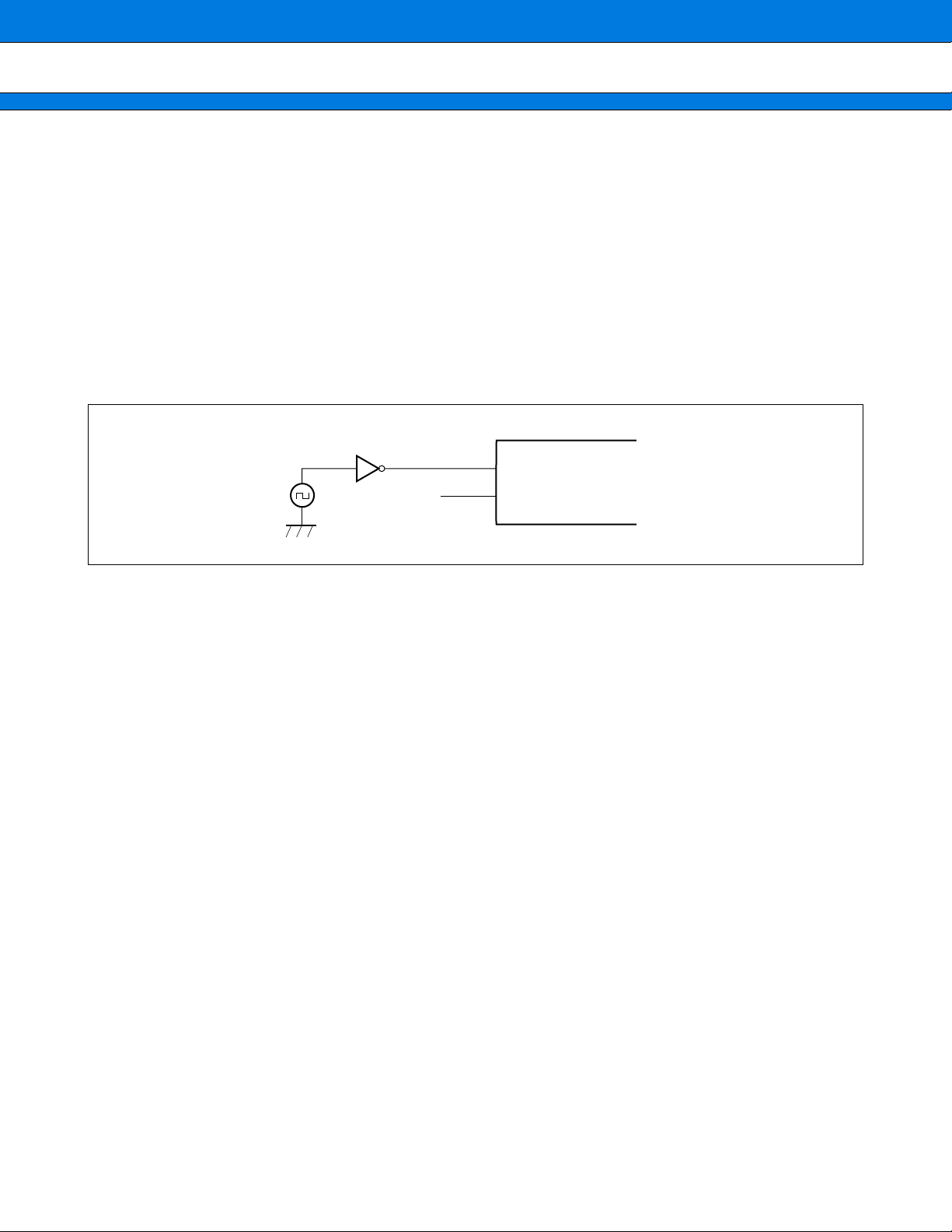
When using an external clock, drive the X0 pin only and leave the X1 pin open.
The figure below shows an example of how to use an external clock.
Example of how to use an external clock
X0
Open circuit
•
Precautions when not using sub-clock mode
X1
MB90520A/520B series
Connect an oscillator to X0A and X1A, even if not using sub-clock mode.
•
Treatment of unused pins
Leaving unused input pins unconnected can cause misoperation or permanent damage to the device due to
latchup. Always pull-up or pull-down unused pins using a 2 kΩ or larger resistor.
If some I/O pins are unused, either set as outputs and leave open circuit or set as inputs and treat in the same
way as input pins.
•
Treatment of N.C. pins
Always leave N.C. (non connect) pins open circuit.
•
Treatment of pins when A/D converter not used
When not using the A/D converter and D/A converter, always connect AV
AVRL = V
•
Sequence for connecting and disconnecting the A/D converter power supply and analog input pins
SS.
Do not apply voltage to the A/D and D/A converter power supply (AV
inputs (AN0 to AN7) until the digital power supply (V
CC) is turned on.
CC = DVCC = AVRH = VCC and AVSS =
CC, AVRH, AVRL, DVCC, DVSS) or analog
When turning the device off, turn off the digital power supply after disconnecting the A/D converter power
supply and analog inputs. When turning the power on or off, ensure that AVRH and DVCC do not e xceed AVCC
(turning the analog and digital power supplies on and off simultaneously is OK) .
•
Shared use of general-purpose I/O ports and LCD controller/driver SEG/COM pins
The SEG08 to SEG31 and COM0 to COM3 pins are shared with general-purpose I/O por ts. The electrical
ratings for SEG08 to SEG23 and COM0 to COM3 are the same as f or CMOS outputs and the electrical ratings
for SEG24 to SEG31 are the same as for N-ch open-drain ports.
18
Page 19
MB90520A/520B Series
•
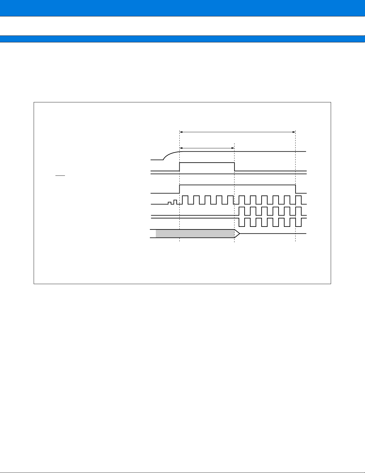
Conditions when output from ports 0 and 1 is undefined
After turning on the power supply, the outputs from ports 0 and 1 are undefined during the oscillation stabilization delay time controlled by the regulator circuit (during the power-on reset) . The figure below shows the
timing.
Note that this undefined output period does not occur on products without an internal regulator circuit as these
products do not have an oscillation stabilization delay time.
Timing chart for undefined output from ports 0 and 1
*2
VCC (Power supply pin)
PONR (Power-on reset) signal
RST (External asynchronous reset) signal
RST (Internal reset) signal
Oscillation clock signal
KA (Internal operating clock A) signal
KB (Internal operating clock B) signal
PORT (port output) signal
Oscillation stabilization delay time
Regulator circuit stabilization
delay time
Undefined output time
*1
*1 : Regulator circuit oscillation stabilization delay time : 217/Oscillation clock frequency
(approx. 8.19 ms for a 16 MHz oscillation clock frequency)
*2 : Oscillation stabilization delay time : 2
18
/Oscillation clock frequency
(approx. 16.38 ms for a 16 MHz oscillation clock frequency)
Note : See the “■ PRODUCT LINEUP” section f or details of which MB90520A/520B series products hav e an internal
regulator circuit.
•
Initialization
The device contains internal registers that are only initialized by a po wer-on reset. To initialize these registers,
restart the power supply.
•
Notes on using the DIV A, Ri and DIVW A, RWi instructions
Set the corresponding bank registers (DTB, ADB, USB, SSB) to “00
H” when using the signed division instruc-
tions “DIV A, Ri” and “DIVW A, RWi”.
If the corresponding bank registers (DTB, ADB, USB, SSB) are set to other than “00
H”, the remainder value
produced by the instruction is not stored in the instruction operand register.
•
Notes on using REALOS
The extended intelligent I/O service (EI
2
OS) cannot be used when using REALOS.
Caution on Operations during PLL Clock Mode
If the PLL clock mode is selected, the microcontroller attempt to be working with the self-oscillating circuit ev en
when there is no external oscillator or external clock input is stopped. Performance of this operation, however,
cannot be guaranteed.
19
Page 20
MB90520A/520B Series
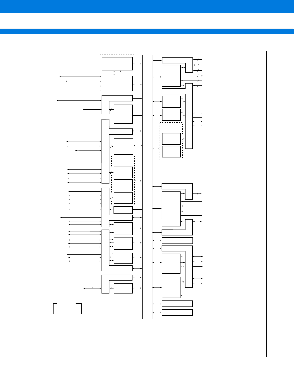
• BLOCK DIAGRAM
F2MC-16LX
CPU
X0, X1
X0A, X1A
RST
HST
P07
P00/INT0 to P06/INT6
P24/AIN0
P25/BIN0
P26/ZIN0/INT7
P20/IC00
P21/IC01
P22/IC10
P23/IC11
P32/OUT0
P33/OUT1
P34/OUT2
P35/OUT3
P31/CKOT
P30
P36/PG00
P37/PG01
P40/PG10
P41/PG11
P42/SIN0
P43/SOT0
P44/SCK0
P45/SIN1
P46/SOT1
P47/SCK1
Main clock
Sub-clock
7
Clock controller
(Includes
timebase timer)
Port 0
7
DTP/
external
interrupt
circuit
Port 2
8/16-bit
3
up/down
counter/
timer 0, 1
16-bit
I/O timer 1
Input
2
capture 0
(ICU)
16-bit
freerun
timer 0
Output
4
compare 0
(OCU)
Clock
output
Port 3
2
8/16-bit
PPG
2
timer 0, 1
UART
(SCI)
SIO ch.1
Port 4
*1
*2
*2
Ports 8, 9*3, A
LCD
controller/
driver
Port 7
16-bit
reload
timer 0
16-bit
reload
timer 1
16-bit
I/O timer 2
Output
compare 1
(OCU)
16-bit
freerun
timer 1
Internal data bus
Port 6
8/10-bit
A/D
converter
Port 2
Interrupt controller
Port 5
SIO ch.2
24
8
P80/SEG16 to P87/SEG23
8
P90/SEG24 to P97/SEG31
8
PA0/SEG08 to PA7/SEG15
8
SEG00 to SEG07
4
4
4
8
V0 to V3
4
P74/COM0 to P77/COM3
P70/TI0/OUT4
P71/TO0/OUT5
P72/TI1/OUT6
P73/TO1/OUT7
8
P60/AN0 to P67/AN7
AVCC
AVSS
AVRH
AVRL
P27/ADTG
P50/SIN2/AIN1
P51/SOT2/BIN1
P52/SCK2/ZIN1
*2
P10/WI0 to P17/WI7
Other pins
MD0 to MD2, C,
V
CC, VSS
Port 1
88
Wakeup
interrupts
8-bit
D/A
converter
× 2 ch
RAM
ROM
2
P53/DA0
P54/DA1
DVCC
DVSS
*1 : The clock control circuit includes the watchdog timer and timebase timer low power consumption control
circuits.
*2 : Incorporates a pull-up register setting register. CMOS level input and output.
*3 : As this port shares pins with the LCD output, the port uses N-ch open-drain circuits.
20
Page 21
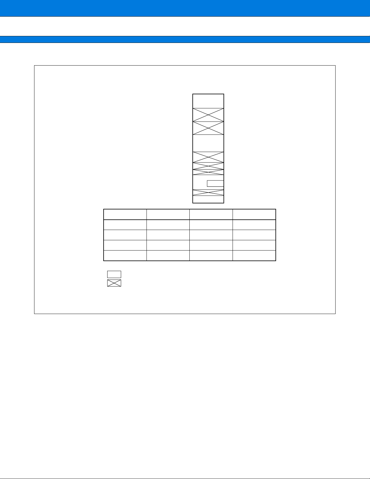
MEMORY MAP
■
MB90520A/520B Series
Single chip mode with mirror function
FFFFFFH
ROM area
Address #1
Part No.
FE0000
010000H
Address #2
004000H
002000H
Address #3
000100H
0000C0H
000000H
Address #1
H
ROM area
(image of
FF bank)
Registers
RAM
Peripherals
*
Address #2*Address #3
MB90522A/B FF0000H 004000H 001100H
MB90523A/B FE0000H 004000H 001100H
MB90F523B FE0000H 004000H 001100H
MB90V520A 001900H
: Internal memory access
: Access prohibited
*
* : The values of addresses #1, #2, and #3 vary by product.
Note : The upper part of 00 bank contains a mirror of the ROM data in FF bank. This is called the mirror ROM
function and enables use of the C compiler’ s small memory model. As the lower 16 bits of the FF bank and
00 bank addresses are the same, tables located in ROM can be referenced without needing to declare far
pointers.
For e xample, accessing 00C000
H actually accesses the contents of ROM at FFC000H. Note that, as the FF
bank ROM area exceeds 48 KBytes, the entire R OM image cannot be mirrored in 00 bank. Accordingly, as
ROM data from FF4000
the range FF4000
H to FFFFFFH is mirrored in 004000H to 00FFFFH, always locate R OM data tables in
H to FFFFFFH.
21
Page 22
MB90520A/520B Series
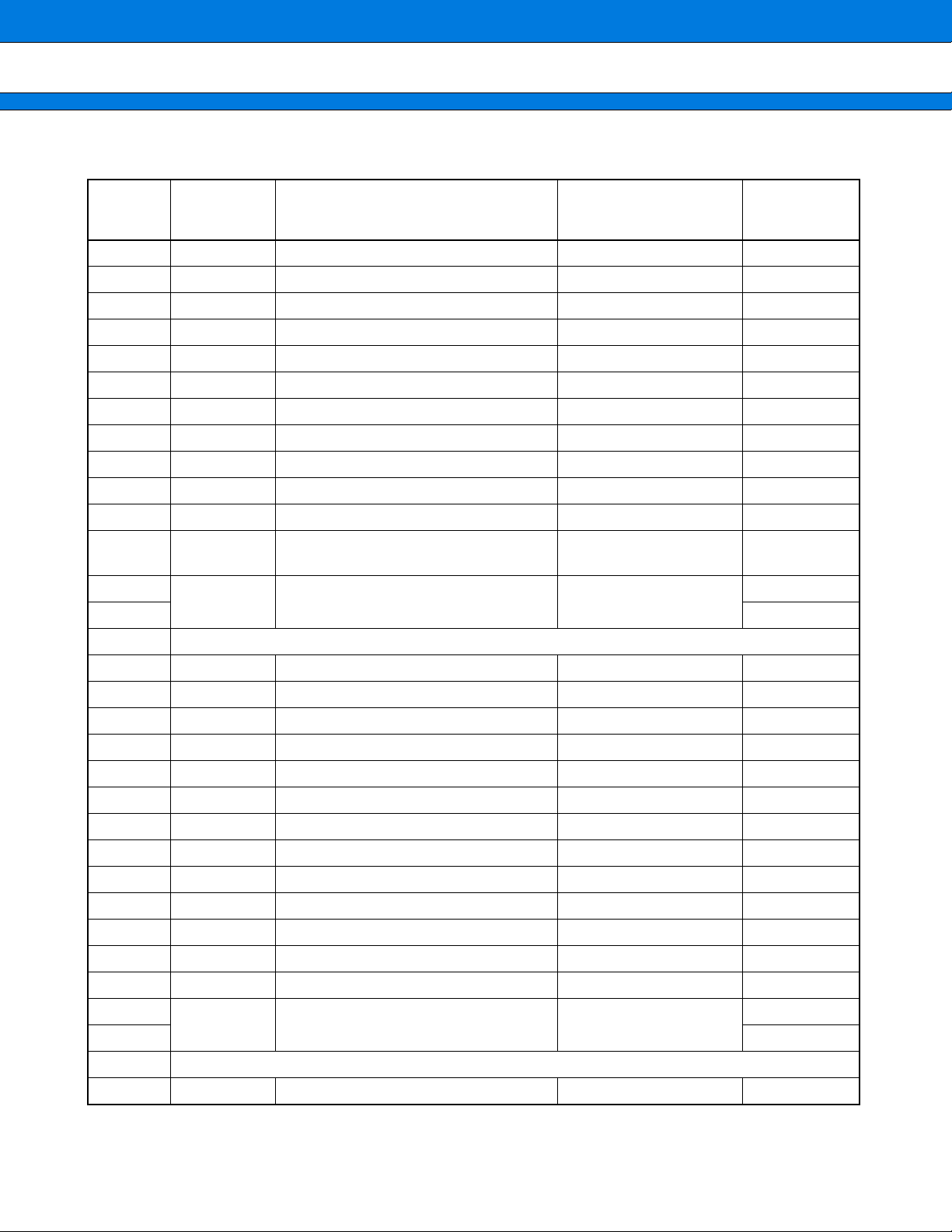
I/O MAP
■
Abbreviated
Address
Register
Name
Register Name Peripheral Name Initial Value
000000
H PDR0 Port 0 data register Port 0 XXXXXXXXB
000001H PDR1 Port 1 data register Port 1 XXXXXXXXB
000002H PDR2 Port 2 data register Port 2 XXXXXXXXB
000003H PDR3 Port 3 data register Port 3 XXXXXXXXB
000004H PDR4 Port 4 data register Port 4 XXXXXXXXB
000005H PDR5 Port 5 data register Port 5 XXXXXXXXB
000006H PDR6 Port 6 data register Port 6 XXXXXXXXB
000007H PDR7 Port 7 data register Port 7 XXXXXXXXB
000008H PDR8 Port 8 data register Port 8 XXXXXXXXB
000009H PDR9 Port 9 data register Port 9 XXXXXXXXB
00000AH PDRA Port A data register Port A XXXXXXXXB
00000BH LCDCMR Port 7/COM pin selection register
00000CH
LCD controller/driver
Port 7,
XXXX 0 0 0 0B
XXXXXXXX
OCP4 OCU compare register ch.4 16-bit I/O timer
00000DH XXXXXXXXB
00000EH (Access prohibited)
00000F
H EIFR Wakeup interrupt flag register Wakeup interrupts XXXXXXX0B
000010H DDR0 Port 0 direction register Port 0 0 0 0 0 0 0 0 0B
B
000011H DDR1 Port 1 direction register Port 1 0 0 0 0 0 0 0 0B
000012H DDR2 Port 2 direction register Port 2 0 0 0 0 0 0 0 0B
000013H DDR3 Port 3 direction register Port 3 0 0 0 0 0 0 0 0B
000014H DDR4 Port 4 direction register Port 4 0 0 0 0 0 0 0 0B
000015H DDR5 Port 5 direction register Port 5 XXX 0 0 0 0 0B
000016H DDR6 Port 6 direction register Port 6 0 0 0 0 0 0 0 0B
000017H DDR7 Port 7 direction register Port 7 0 0 0 0 0 0 0 0B
000018H DDR8 Port 8 direction register Port 8 0 0 0 0 0 0 0 0B
000019H DDR9 Port 9 direction register Port 9 0 0 0 0 0 0 0 0B
00001AH DDRA Port A direction register Port A 0 0 0 0 0 0 0 0B
00001BH ADER Analog input enable register Port 6, A/D converter 1 1 1 1 1 1 1 1B
00001CH
XXXXXXXX
OCP5 OCU compare register ch.5 16-bit I/O timer
00001DH XXXXXXXXB
00001EH (Access prohibited)
00001FH EICR Wakeup interrupt enable register Wakeup interrupts 0 0 0 0 0 0 0 0B
(Continued)
B
22
Page 23
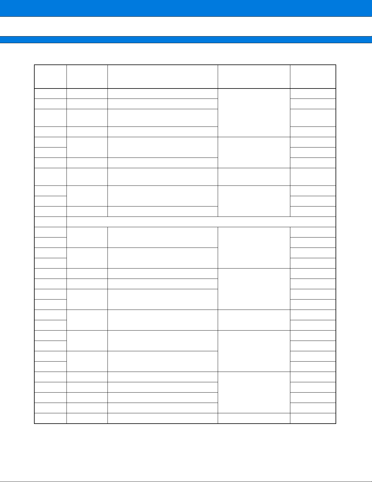
Address
Abbreviated
Register
Name
MB90520A/520B Series
Register Name Peripheral Name Initial Value
000020
H SMR Serial mode register
0 0 0 0 0 0 0 0B
000021H SCR Serial control register 0 0 0 0 0 1 0 0B
UART
000022H
SIDR/
SODR
Serial input data register/
Serial output data register
(SCI)
XXXXXXXXB
000023H SSR Serial status register 0 0 0 0 1 X 0 0B
000024H
000025H 0 0 0 0 0 0 1 0B
SMCS1 Serial mode control status register 1
Extended I/O serial
interface 1
XXXX
0 0 0 0B
000026H SDR1 Serial data register 1 XXXXXXXXB
000027H CDCR
Communication prescaler control
register
000028H
SMCS2 Serial mode control status register 2
000029H 0 0 0 0 0 0 1 0B
Communication prescaler
register
Extended I/O serial
interface 2
0 XXX 1 1 1 1B
XXXX
0 0 0 0B
00002AH SDR2 Serial data register 2 XXXXXXXXB
00002BH (Access prohibited)
00002C
H
0
0 0 0 XX 0 0B
OCS45 OCU control status register ch.45
00002DH XXX 0 0 0 0 0B
16-bit I/O timer
00002EH
0 0 0 XX 0 0B
0
OCS67 OCU control status register ch.67
00002FH XXX 0 0 0 0 0B
000030H ENIR DTP/interrupt enable register
000031H EIRR DTP/interrupt request register XXXXXXXXB
000032H
DTP /external interrupt
circuit
0 0 0 0 0 0 0 0B
0
0 0 0 0 0 0 0B
ELVR Request level setting register
000033H 0 0 0 0 0 0 0 0B
000034H
XXXXXXXX
OCP6 OCU compare register ch.6 16-bit I/O timer
000035H XXXXXXXXB
000036H
0
0 0 0 0 0 0 0B
ADCS A/D control status register
000037H 0 0 0 0 0 0 0 0B
8/10-bit A/D converter
000038H
XXXXXXXX
ADCR A/D data register
000039H 0 0 0 0 1 XXXB
00003AH DADR0 D/A converter data register ch.0
XXXXXXXXB
00003BH DADR1 D/A converter data register ch.1 XXXXXXXXB
8-bit D/A converter
00003CH DACR0 D/A control register 0 XXXXXXX 0B
00003DH DACR1 D/A control register 1 XXXXXXX 0B
00003EH CLKR Clock output enable register Clock monitor function XXXX 0 0 0 0B
(Continued)
B
B
23
Page 24
MB90520A/520B Series
Abbreviated
Address
Register
Name
Register Name Peripheral Name Initial Value
00003F
000040
H (Access prohibited)
H PRLL0 PPG0 reload register L
XXXXXXXXB
000041H PRLH0 PPG0 reload register H XXXXXXXXB
000042H PRLL1 PPG1 reload register L XXXXXXXXB
000043H PRLH1 PPG1 reload register H XXXXXXXXB
8/16-bit PPG timer 0, 1
000044H PPGC0 PPG0 operation mode control register 0 X 0 0 0 XX 1B
000045H PPGC1 PPG1 operation mode control register 0 X 0 0 0 0 0 1B
000046H PPGOE PPG0, 1 output control register 0 0 0 0 0 0 0 0B
000047H (Access prohibited)
000048
H
0
0 0 0 0 0 0 0B
TMCSR0 Timer control status register ch.0
000049H XXXX 0 0 0 0B
16-bit reload timer 0
00004AH
00004BH XXXXXXXXB
TMR0/
TMRLR0
16-bit timer register ch.0/
16-bit reload register ch.0
00004CH
XXXXXXXX
0
0 0 0 0 0 0 0B
TMCSR1 Timer control status register ch.1
00004DH XXXX 0 0 0 0B
16-bit reload timer 1
00004EH
00004FH XXXXXXXXB
TMR1/
TMRLR1
16-bit timer register ch.1/
16-bit reload register ch.1
000050H
XXXXXXXX
XXXXXXXX
IPCP0 ICU data register ch.0
000051H XXXXXXXXB
B
B
B
000052H
16-bit I/O timer
XXXXXXXX
IPCP1 ICU data register ch.1
000053H XXXXXXXXB
000054H ICS01 ICU control status register 0 0 0 0 0 0 0 0B
000055H (Access prohibited)
000056
H
0 0 0 0 0 0 0B
0
TCDT0 Freerun timer data register 0
000057H 0 0 0 0 0 0 0 0B
16-bit I/O timer
000058H TCCS0 Freerun timer control status register 0 0 0 0 0 0 0 0 0B
000059H (Access prohibited)
00005AH
XXXXXXXX
OCP0 OCU compare register ch.0
00005BH XXXXXXXXB
00005CH
OCP1 OCU compare register ch.1
16-bit I/O timer
XXXXXXXX
00005DH XXXXXXXXB
00005EH
XXXXXXXX
OCP2 OCU compare register ch.2
00005FH XXXXXXXXB
24
B
B
B
B
(Continued)
Page 25
Address
Abbreviated
Register
Name
MB90520A/520B Series
Register Name Peripheral Name Initial Value
000060
H
XXXXXXXX
OCP3 OCU compare register ch.3
000061H XXXXXXXXB
000062H
OCS01 OCU control status register ch.0, ch.1
16-bit I/O timer
0
0 0 0 XX 0 0B
000063H XXX 0 0 0 0 0B
000064H
0 0 0 XX 0 0B
0
OCS23 OCU control status register ch.2, ch.3
000065H XXX 0 0 0 0 0B
000066H
0 0 0 0 0 0 0B
0
TCDT1 Freerun timer data register 1
000067H 0 0 0 0 0 0 0 0B
16-bit I/O timer
000068H TCCS1 Freerun timer control status register 1 0 0 0 0 0 0 0 0B
000069H (Access prohibited)
00006A
H LCR0 LCDC control register 0
0 0 0 1 0 0 0 0B
LCD controller/driver
00006BH LCR1 LCDC control register 1 0 0 0 0 0 0 0 0B
00006CH
XXXXXXXX
OCP7 OCU compare register ch.7 16-bit I/O timer
00006DH XXXXXXXXB
00006EH (Access prohibited)
00006F
H ROMM ROM mirror function selection register
ROM mirror function
selection module
XXXXXXX1B
000070H
to
00007F
H
VRAM Data memory for LCD display LCD controller/driver XXXXXXXXB
B
B
000080H UDCR0 Up/down count register 0
0 0 0 0 0 0 0 0B
000081H UDCR1 Up/down count register 1 0 0 0 0 0 0 0 0B
000082H RCR0 Reload compare register 0 0 0 0 0 0 0 0 0B
8/16-bit up/down
counter/timer 0, 1
000083H RCR1 Reload compare register 1 0 0 0 0 0 0 0 0B
000084H CSR0 Counter status register 0 0 0 0 0 0 0 0 0B
000085H (Reserved)
000086H
CCR0 Counter control register 0
000087H 0 0 0 0 0 0 0 0B
*3
8/16-bit up/down
counter/timer 0, 1
X
0 0 0 0 0 0 0B
000088H CSR1 Counter status register 1 0 0 0 0 0 0 0 0B
000089H (Reserved)
00008AH
CCR1 Counter control register 1
00008BH X 0 0 0 0 0 0 0B
00008CH RDR0
00008DH RDR1
Port 0
input pull-up resistor setup register
Port 1
input pull-up resistor setup register
*3
8/16-bit up/down
counter/timer 0, 1
X
0 0 0 0 0 0 0B
Port 0 0 0 0 0 0 0 0 0B
Port 1 0 0 0 0 0 0 0 0B
(Continued)
25
Page 26
MB90520A/520B Series
Abbreviated
Address
Register
Name
Register Name Peripheral Name Initial Value
00008E
H RDR4
00008FH
to
00009D
H
00009EH PACSR Address detection control register
00009FH DIRR
0000A0H LPMCR
Port 4
input pull-up resistor setup register
(Access prohibited)
(Area reserved for system use)
Delayed interrupt request output/clear
register
Low power consumption mode control
register
Port 4 0 0 0 0 0 0 0 0B
*4
Address match detection
function
Delayed interrupt
generation module
Low power consumption
0 0 0 0 0 0 0 0B
XXXXXXX 0B
0
0 0 1 1 0 0 0B
(standby) mode
0000A1H CKSCR Clock selection register 1 1 1 1 1 1 0 0B
0000A2H
to
0000A7
0000A8
H
H WDTC Watchdog timer control register Watchdog timer XXXXXXXXB
(Access prohibited)
0000A9H TBTC Timebase timer control register Timebase timer 1 XX 0 0 0 0 0B
0000AAH WTC Clock timer control register Clock timer 1 X 0 0 1 0 0 0B
0000ABH
to
0000AD
H
(Access prohibited)
0000AE
H FMCS Flash memory control status register 1 Mbit flash memory 0 0 0 X 0 0 0 0B
0000AFH (Access prohibited)
0000B0
H ICR00 Interrupt control register 00
0 0 0 0 0 1 1 1B
0000B1H ICR01 Interrupt control register 01 0 0 0 0 0 1 1 1B
0000B2H ICR02 Interrupt control register 02 0 0 0 0 0 1 1 1B
0000B3H ICR03 Interrupt control register 03 0 0 0 0 0 1 1 1B
0000B4H ICR04 Interrupt control register 04 0 0 0 0 0 1 1 1B
0000B5H ICR05 Interrupt control register 05 0 0 0 0 0 1 1 1B
0000B6H ICR06 Interrupt control register 06 0 0 0 0 0 1 1 1B
Interrupt controller
0000B7H ICR07 Interrupt control register 07 0 0 0 0 0 1 1 1B
0000B8H ICR08 Interrupt control register 08 0 0 0 0 0 1 1 1B
0000B9H ICR09 Interrupt control register 09 0 0 0 0 0 1 1 1B
0000BAH ICR10 Interrupt control register 10 0 0 0 0 0 1 1 1B
0000BBH ICR11 Interrupt control register 11 0 0 0 0 0 1 1 1B
0000BCH ICR12 Interrupt control register 12 0 0 0 0 0 1 1 1B
0000BDH ICR13 Interrupt control register 13 0 0 0 0 0 1 1 1B
(Continued)
26
Page 27
(Continued)
Address
Abbreviated
Register
Name
MB90520A/520B Series
Register Name Peripheral Name Initial Value
0000BE
H ICR14 Interrupt control register 14
0 0 0 0 0 1 1 1B
Interrupt controller
0000BFH ICR15 Interrupt control register 15 0 0 0 0 0 1 1 1B
0000C0H
to
0000FF
(Access prohibited)
H
*1
000100H
to
00####
(RAM area)
H
*2
00####H
to
001FEF
001FF0H
001FF1H
001FF2H
001FF3H
001FF4H
(Reserved area)
H
Detection address setting register 0
(low byte)
PADR0
Detection address setting register 0
(middle byte)
Detection address setting register 0
(high byte)
Detection address setting register 1
(low byte)
PADR1
Detection address setting register 1
(middle byte)
*3
XXXXXXXX
XXXXXXXXB
XXXXXXXXB
Address match
detection function
XXXXXXXX
XXXXXXXXB
B
B
001FF5H
Detection address setting register 1
(high byte)
XXXXXXXXB
001FF6H
to
001FFF
(Reserved area)
H
*3
Initial value notation
0 : Initial value of bit is “0”.
1 : Initial value of bit is “1”.
X : Initial value of bit is undefined.
*1 : Access is prohibited to the address range 0000C0
H to 0000FFH. See the “■ MEMORY MAP” section.
*2 : See the “■ MEMORY MAP” section for details of the “ (RAM area) ”.
*3 : “ (Reserved areas) ” are addresses used internally by the system and may not be used.
*4 : The “ (Area reserved for system use) ” contains setting registers used by the evaluation tools.
Notes : • LPMCR, CKSCR, and WDTC are initialized by some types of reset and not by others. The initial values
listed are for the case when the registers are initialized.
• The boundary address “####
H” between the “ (RAM area) ” and “ (Reserved area) ” differs depending on
the product. See the “■ MEMORY MAP” section for details.
• OCU compare registers ch.0 to ch.3 use 16-bit freerun timer 0 and OCU compare registers ch.4 to ch.7
use 16-bit freerun timer 1. Note that 16-bit freerun timer 0 is also used by input capture 0 and 1 (ICU) .
27
Page 28
MB90520A/520B Series
INTERRUPTS, INTERRUPT VECTORS, AND INTERRUPT CONTROL REGISTERS
■
2
EI
Interrupt
Reset #08 FFFFDC
INT 9 instruction #09 FFFFD8
Exception #10 FFFFD4H
OS
Support
×
×
×
8/10-bit A/D converter #11 FFFFD0
Timebase timer #12 FFFFCCH
×
DTP0/DTP1
(external interrupt 0/external interrupt 1)
16-bit freerun timer 0 overflow #14 FFFFC4H
×
Interrupt Vector Interrupt Control Register
Priority
No. Address ICR Address
H High
H
H
ICR00 0000B0H
#13 FFFFC8H
ICR01 0000B1H
Extended I/O serial interface 1 #15 FFFFC0H
Wakeup interrupt #16 FFFFBCH
×
ICR02 0000B2H
Extended I/O serial interface 2 #17 FFFFB8H
DTP2/DTP3
(external interrupt 2/external interrupt 3)
8/16-bit PPG timer 0 counter borrow #19 FFFFB0H
×
DTP4/DTP5
(external interrupt 4/external interrupt 5)
#18 FFFFB4H
#20 FFFFACH
ICR03 0000B3H
ICR04 0000B4H
8/16-bit up/down counter/timer 0
compare match
8/16-bit up/down counter/timer 0
overflow, up/down direction change
8/16-bit PPG timer 1 counter borrow #23 FFFFA0H
×
DTP6/DTP7
(external interrupt 6/external interrupt 7)
#21 FFFFA8H
#22 FFFFA4H
#24 FFFF9CH
Output compare 1 (OCU) ch.4, ch.5 match #25 FFFF98H
Clock timer #26 FFFF94H
×
Output compare 1 (OCU) ch.6, ch.7 match #27 FFFF90H
16-bit freerun timer 1 overflow #28 FFFF8CH
8/16-bit up/down counter/timer 1
compare match
8/16-bit up/down counter/timer 1
overflow, up/down direction change
×
#29 FFFF88H
#30 FFFF84H
Input capture 0 (ICU) capture #31 FFFF80H
Input capture 1 (ICU) capture #32 FFFF7CH
Output compare 0 (OCU) ch.0 match #33 FFFF78H
Output compare 0 (OCU) ch.1 match #34 FFFF74H
ICR05 0000B5H
ICR06 0000B6H
ICR07 0000B7H
ICR08 0000B8H
ICR09 0000B9H
ICR10 0000BAH
ICR11 0000BBH
28
(Continued)
Page 29
(Continued)
Interrupt
2
OS
EI
Support
MB90520A/520B Series
Interrupt Vector Interrupt Control Register
Priority
No. Address ICR Address
Output compare 0 (OCU) ch.2 match #35 FFFF70
H
ICR12 0000BCH
Output compare 0 (OCU) ch.3 match #36 FFFF6CH
UART (SCI) receive complete #37 FFFF68H
ICR13 0000BDH
16-bit reload timer 0 #38 FFFF64H
UART (SCI) send complete #39 FFFF60H
ICR14 0000BEH
16-bit reload timer 1 #40 FFFF5CH
Flash memory #41 FFFF58H
Delayed interrupt generation module #42 FFFF54H Low
×
×
ICR15 0000BFH
: Supported
×
: Not supported
: Supported, includes EI
2
OS stop function
29
Page 30
MB90520A/520B Series
PERIPHERAL RESOURCES
■
1. I/O Ports
• The I/O ports can be used as general-purpose I/O ports (parallel I/O ports) . The MB90520A and 520B series
have 11 ports (85 pins) . The ports share pins with the inputs and outputs of the peripheral functions.
• The port data registers (PDR) are used to output data to the I/O pins and capture the input signals from the
I/O ports.
Similarly, the port direction registers (DDR) set the I/O direction (input or output) for each individual port bit.
• The following tables list the I/O ports and peripheral functions with which they share pins.
Pin Name
(Port)
Pin Name (Peripheral) Peripheral Function that Shares Pin
Port 0
Port 1 P10 − P17 WI0 − WI7 Wakeup interrupts
Port 2
Port 3
Port 4
Port 5
Port 6 P60 − P67 AN0 − AN7 8/16-bit A/D converter
P00 − P06 INT0 − INT6 External interrupts
P07 Not shared
P20 − P23 IN00 − IN11 Input capture (unit 0)
P24, P25 AIN0, BIN0 8/16-bit up/down counter/timer 0
P26 ZIN0/INT7 8/16-bit up/down counter/timer 0, external interrupt
P30 Not shared
P31 CKOT Clock monitor function
P32 − P35 OUT0 − OUT3 Output compare (unit 0)
P36, P37 PPG00, PPG01 8/16-bit PPG timer 0
P40, P41 PPG10, PPG11 8/16-bit PPG timer 1
P42 − P44 SIN0, SOT0, SCK0 UART (SCI)
P45 − P47 SIN1, SOT1, SCK1 Extended I/O serial interface 0
SIN2/AIN1,
P50 − P52
P53, P54 DA0, DA1 8-bit D/A converter
SOT1/BIN1,
SCK1/ZIN1
8/16-bit up/down counter/timer 0
Extended I/O serial interface 1
TIN0/OUT4,
Port 7
P70 − P73
P74 − P77 COM0 − COM3 LCD control driver common output
Port 8 P80 − P87 SEG16 − SEG23 LCD control driver segment output
Port 9 P90 − P97 SEG24 − SEG31 LCD control driver segment output
Port A PA0 − PA7 SEG8 − SEG15 LCD control driver segment output
Notes
• Port 9 contains general-purpose I/O ports with N-ch open-drain output circuits.
• Connect an external pull-up resistor when using port 9 pins as outputs.
• Port 6 shares pins with the analog inputs. When using port 6 as a general-purpose por t, ensure that the
corresponding analog input enable register (ADER) bits are set to “0”. ADER is initialized to “FF
30
TOT0/OUT5,
TIN1/OUT6,
TOT1/OUT7
16-bit reload timers 0, 1
Output compare (unit 1)
H” after a reset.
Page 31

MB90520A/520B Series
•
Block diagrams
P00 to P07, P10 to P17
Pull-up resistor
option connect/
disconnect setting
Pch
Pin
PDR (Port data register)
PDR read
Output latch
PDR write
DDR (Port direction register)
Internal data bus
Direction latch
DDR write
DDR read
Peripheral function input
Pch
Nch
Standby control (SPL = 1)
Standby control : Controls stop mode (SPL = 1) , time-base-timer mode (SPL = 1) , clock mode (SPL = 1) ,
and hardware standby mode
P20 to P27
Peripheral function input
PDR (Port data register)
PDR read
PDR write
DDR (Port direction register)
Internal data bus
Direction latch
DDR write
DDR read
Output latch
Pch
Pin
Nch
Standby control (SPL = 1)
Standby control : Controls stop mode (SPL = 1) , time-base-timer mode (SPL = 1) , clock mode (SPL = 1) ,
and hardware standby mode
31
Page 32

MB90520A/520B Series
P40 to P47
Peripheral function input*
Pull-up resistor
option connect/
disconnect setting
PDR (Port data register)
PDR read
Output latch
PDR write
DDR (Port direction register)
Internal data bus
DDR write
DDR read
Direction latch
Peripheral function output*
Peripheral function
output approval*
Standby control (SPL = 1)
Pch
Pch
Pin
Nch
Standby control : Controls stop mode (SPL = 1) , time-base-timer mode (SPL = 1) , clock mode (SPL = 1) ,
and hardware standby mode
* : Peripheral function I/O is equivalent to I/O of peripheral function.
P30 to P37, P50 to P52, P70 to P73
Peripheral function input*
PDR (Port data register)
PDR read
Output latch
PDR write
DDR (Port direction register)
Internal data bus
DDR write
DDR read
Direction latch
Peripheral function output*
Peripheral function
output approval*
Pch
Pin
Nch
Standby control (SPL = 1)
Standby control : Controls stop mode (SPL = 1) , time-base-timer mode (SPL = 1) , clock mode (SPL = 1) ,
and hardware standby mode
* : Peripheral function I/O is equivalent to I/O of peripheral function.
32
Page 33

P53, P54
MB90520A/520B Series
D/A analog pin
output approval
D/A analog output
PDR (Port data register)
PDR read
Output latch
PDR write
DDR (Port direction register)
Internal data bus
DDR write
Direction latch
Pch
Pin
Nch
DDR read
Standby control (SPL = 1)
Standby control : Controls stop mode (SPL = 1) , time-base-timer mode (SPL = 1) , clock mode (SPL = 1) ,
and hardware standby mode
P74 to P77
Common pin
output approval
LCD common output
PDR (Port data register)
PDR read
Output latch
PDR write
DDR (Port direction register)
Internal data bus
DDR write
Direction latch
Pch
Pin
Nch
DDR read
Standby control (SPL = 1)
Standby control : Controls stop mode (SPL = 1) , time-base-timer mode (SPL = 1) , clock mode (SPL = 1) ,
and hardware standby mode
33
Page 34

MB90520A/520B Series
P60 to P67
PDR (Port data register)
PDR read
Output latch
PDR write
DDR (Port direction register)
Internal data bus
DDR write
Direction latch
Analog input
Pch
Pin
Nch
DDR read
Standby control (SPL = 1)
Standby control : Controls stop mode (SPL = 1) , time-base-timer mode (SPL = 1) , clock mode (SPL = 1) ,
and hardware standby mode
P80 to P87, PA0 to PA7
Segment pin
output approval
LCD Segment output
PDR (Port data register)
PDR read
Output latch
PDR write
DDR (Port direction register)
Internal data bus
DDR write
Direction latch
Pch
Pin
Nch
DDR read
Standby control (SPL = 1)
Standby control : Controls stop mode (SPL = 1) , time-base-timer mode (SPL = 1) , clock mode (SPL = 1) ,
and hardware standby mode
34
Page 35

P90 to P97
MB90520A/520B Series
Segment pin
output approval
LCD Segment output
PDR (Port data register)
PDR read
Output latch
PDR write
DDR (Port direction register)
Internal data bus
DDR write
DDR read
Direction latch
Nch
Standby control (SPL = 1)
Pin
Standby control : Controls stop mode (SPL = 1) , time-base-timer mode (SPL = 1) , clock mode (SPL = 1) ,
and hardware standby mode
35
Page 36

MB90520A/520B Series
2. Timebase Timer
• The timebase timer is an 18-bit freerun timer (timebase timer/counter) that counts up synchronized with the
main clock (oscillation clock : HCLK divided by 2) .
• The timer can generate interrupt requests at a specified interval, with four different interval time settings
available.
• The timer supplies the operating clock f or peripheral functions including the oscillation stabilization delay timer
and watchdog timer.
•
Timebase timer interval settings
Internal Count Clock Period Interval Time
12
2
/HCLK (approx. 1.024 ms)
14
/HCLK (approx. 4.096 ms)
2/HCLK (0.5 µs)
2
16
2
/HCLK (approx. 16.384 ms)
19
2
/HCLK (approx. 131.072 ms)
• HCLK : Oscillation clock frequency
• The values enclosed in ( ) indicate the times for a clock frequency of 4 MHz.
•
Period of clocks supplied from timebase timer
Peripheral Function Clock Period
10
2
/HCLK (approx. 0.256 ms)
13
/HCLK (approx. 2.048 ms)
Oscillation stabilization delay
for the main clock
Watchdog timer
PPG timer 2
2
15
2
/HCLK (approx. 8.192 ms)
17
2
/HCLK (approx. 32.768 ms)
12
2
/HCLK (approx. 1.024 ms)
14
/HCLK (approx. 4.096 ms)
2
16
2
/HCLK (approx. 16.384 ms)
19
2
/HCLK (approx. 131.072 ms)
9
/HCLK (approx. 0.128 ms)
• HCLK : Oscillation clock frequency
• The values enclosed in ( ) indicate the times for a clock frequency of 4 MHz.
36
Page 37

MB90520A/520B Series
•
Block diagram
HCLK divided
by 2
Timebase timer/counter
1
× 22× 2
× 2
Reset
Clear stop mode, etc.
Switch clock mode
Timebase timer control register
Timebase timer interrupt signal
3
*1
*2
*3
(TBTC)
To PPG timer
× 28× 29× 210× 211× 212× 213× 214× 215× 216× 217× 2
Counter clear
circuit
TBOF clear TBOF set
OF
OF
Interval timer
selector
TBIE TBOF TBR TBC1 TBC0
OF
To watchdog timer
18
OF
To oscillation
stabilization delay
time selector
in clock controller
OF : Overflow
HCLK : Oscillation clock frequency
*1 : Power-on reset, release of hardware standby mode, watchdog reset
*2 : Clear stop mode, main clock mode, PLL clock mode, and pseudo-clock mode
*3 : Main → PLL clock, Sub → main clock, Sub → PLL clock
The actual interrupt request number for the timebase timer is :
Interrupt request number : #12 (0C
H)
37
Page 38

MB90520A/520B Series
3. Watchdog Timer
• The watchdog timer is a timer/counter used to detect faults such as program runaway.
• The watchdog timer is a 2-bit counter that counts the clock signal from the timebase timer or clock timer.
• Once started, the watchdog timer must be cleared before the 2-bit counter overflows. If an overflow occurs,
the CPU is reset.
•
Interval time for the watchdog timer
HCLK : Oscillation Clock (4 MHz) SCLK : Sub-Clock (8.192 kHz)
Min Max Clock Period Min Max Clock Period
Approx. 3.58 ms Approx. 4.61 ms 2
Approx. 14.33 ms Approx. 18.30 ms 2
Approx. 57.23 ms Approx. 73.73 ms 2
Approx. 458.75 ms Approx. 589.82 ms 2
* : The difference between the maximum and minim um watchdog timer interval times is due to the timing when the
counter is cleared.
* : As the watchdog timer is a 2-bit counter that counts the carry-up signal from the timebase timer or clock timer,
clearing the timebase timer (when operating on HCLK) or the clock timer (when operating on SCLK) lengthens
the time until the watchdog timer reset is generated.
14
± 211 / HCLK Approx. 0.438 s Approx. 0.563 s 212 ± 29 / SCLK
16
± 213 / HCLK Approx. 3.500 s Approx. 4.500 s 215 ± 212 / SCLK
18
± 215 / HCLK Approx. 7.000 s Approx. 9.000 s 216 ± 213 / SCLK
21
± 218 / HCLK Approx. 14.00 s Approx. 18.00 s 217 ± 214 / SCLK
•
Watchdog timer count clock
WTC : WDCS
HCLK : Oscillation clock
PCLK : PLL clock
SCLK : Sub-clock
“0” Count the clock timer output.
Count the clock timer output.
“1” Count the timebase timer output.
• Events that stop the watchdog timer
1 : Stop due to a power-on reset
2 : Reset due to recovery from hardware standby mode
3 : Watchdog reset
• Events that clear the watchdog timer
1 : External reset input from the RST pin.
2 : Writing “0” to the software reset bit.
3 : Writing “0” to the watchdog control bit (second and subsequent times) .
4 : Changing to sleep mode (clears the watchdog timer and temporarily halts the count) .
5 : Changing to pseudo-clock mode (clears the watchdog timer and temporarily halts the count) .
6 : Changing to clock mode (clears the watchdog timer and temporarily halts the count) .
7 : Changing to stop mode (clears the watchdog timer and temporarily halts the count) .
38
Page 39

MB90520A/520B Series
•
Block diagram
Change to sleep mode
Change to pseudo-clock mode
Change to clock mode
Change to stop mode
Main clock
(HCLK divided by 2)
Reset
Watchdog timer control register (WDTC)
PONR STBR WRST ERST SRST WTE WT1 WT0
Watchdog timer
Counter
clear
control circuit
(Timebase timer/counter)
1
× 2
× 2
(Clock counter)
2
Start
Counter
clock
selector
4
2
× 28× 29× 210× 211× 212× 213× 214× 215× 216× 217× 2
2-bit
counter
Clear
Watchdog timer
reset
generation circuit
To
internal
reset
circuit
4
18
Sub-clock
HCLK : Oscillation clock frequency
× 21× 2
2
× 25× 26× 27× 28× 29× 210× 211× 212× 213× 214× 2
15
39
Page 40

MB90520A/520B Series
4. 8/16-bit PPG (Programmable Pulse Generator) Timers 0 and 1
The 8/16-bit PPG timer is a two-channel reload timer module (PPG0 and PPG1) that can generate pulse outputs
with the periods specified in the table below and with duty ratios between 0 and 100%. Note that the pulse
periods are different depending on the operation mode.
Operation
Mode
8-bit
PPG output
Independent
2ch operation
mode
16-bit
PPG output
operation
mode
8 + 8-bit
PPG output
operation
*1
mode
PPG00, PPG01 (PPG ch0) PPG10, PPG11 (PPG ch1)
Count Clock
φ/1 (62.5 ns) 1/φ to 2
φ/2 (125 ns) 2/φ to 2
φ/4 (250 ns) 2
φ/8 (500 ns) 2
φ/16 (1000 ns) 2
HCLK/512 (128 µs)
φ/1 (62.5 ns) 1/φ to 2
φ/2 (125 ns) 2/φ to 2
φ/4 (250 ns) 2
φ/8 (500 ns) 2
φ/16 (1000 ns) 2
HCLK/512 (128 µs)
*2
Interval Time
8
/φ 1/φ to 29/φ 1/φ to 28/φ 1/φ to 29/φ
9
/φ 22/φ to 210/φ 2/φ to 29/φ 22/φ to 210/φ
2
/φ to 210/φ 23/φ to 211/φ 22/φ to 210/φ 23/φ to 211/φ
3
/φ to 211/φ 24/φ to 212/φ 23/φ to 211/φ 24/φ to 212/φ
4
/φ to 212/φ 25/φ to 213/φ 24/φ to 212/φ 25/φ to 213/φ
9
/HCLK to
2
17
2
/HCLK
16
/φ 1/φ to 217/φ 1/φ to 216/φ 1/φ to 217/φ
17
/φ 22/φ to 218/φ 2/φ to 217/φ 22/φ to 218/φ
2
/φ to 218/φ 23/φ to 219/φ 22/φ to 218/φ 23/φ to 219/φ
3
/φ to 219/φ 24/φ to 220/φ 23/φ to 219/φ 24/φ to 220/φ
4
/φ to 220/φ 25/φ to 221/φ 24/φ to 220/φ 25/φ to 221/φ
9
/HCLK to
2
25
2
/HCLK
Output Pulse
Width
10
/HCLK to
2
18
2
/HCLK
10
/HCLK to
2
26
2
/HCLK
Interval Time
9
/HCLK to
2
17
2
/HCLK
9
/HCLK to
2
25
2
/HCLK
Output Pulse
10
2
2
10
2
2
φ/1 (62.5 ns) 1/φ to 26/φ 1/φ to 29/φ 1/φ to 216/φ 1/φ to 217/φ
φ/2 (125 ns) 2/φ to 2
φ/4 (250 ns) 2
φ/8 (500 ns) 2
φ/16 (1000 ns) 2
HCLK/512 (128 µs)
2
3
4
2
2
9
/φ 22/φ to 210/φ 2/φ to 217/φ 22/φ to 218/φ
/φ to 210/φ 23/φ to 211/φ 22/φ to 218/φ 23/φ to 219/φ
/φ to 211/φ 24/φ to 212/φ 23/φ to 219/φ 24/φ to 220/φ
/φ to 212/φ 25/φ to 213/φ 24/φ to 220/φ 25/φ to 221/φ
9
/HCLK to
17
/HCLK
10
/HCLK to
2
18
2
/HCLK
9
/HCLK to
2
25
2
/HCLK
10
2
2
Width
/HCLK to
18
/HCLK
/HCLK to
26
/HCLK
/HCLK to
26
/HCLK
*1 : 8 + 8-bit PPG output operation mode consists of using the lower 8 bits as a prescaler for the PPG timer.
*2 : The values enclosed in ( ) indicate the times for a machine clock frequency of 16 MHz.
40
Page 41

MB90520A/520B Series
• PPG timer channels and PPG pins
The figure below shows the relationship between the 8/16-bit PPG channels and PPG pins on the MB90520A/
520B series.
PPG0
PPG1
Pin
PPG00 output pin
Pin
PPG01 output pin
Pin
PPG10 output pin
Pin
PPG11 output pin
41
Page 42

MB90520A/520B Series
•
Block diagram
8/16-bit PPG timer 0
PRLH0
("H" level register)
PPG0 temporary
buffer (PRLBH0)
Reload register
"L" level/"H" level
Count start value
PPG0 down counter
PPG0 reload
register
("L" level register)
selector
(PCNT0)
PRLL0
Reload
Select signal
Underflow
PEN0 PE00 PIE0
Clear
Pulse selector
"H" level data bus
"L" level data bus
PPG0 operation mode control register
(PPGC0)
PUF0 Reserved
R
SQ
2
Interrupt
request output
Operation mode control signal
PPG1 underflow
PPG0 underflow
(to PPG1)
CLK
Timebase timer output
(HCLK/512)
Peripheral clock (φ/1)
Peripheral clock (φ/2)
Peripheral clock (φ/4)
Peripheral clock (φ/8)
Peripheral clock (φ/16)
: Undefined
Reserved : Reserved bit
HCLK : Oscillation clock frequency
φ : Machine clock frequency
PPG0
Invert
PCS2 PCS0 PCM2
PPG01 output control register (PPGOE)
output latch
Count
clock
selector
3
Select signal
PCS1
PPG output control circuit
PCM1 PCM0 PE11 PE01
Pin
PPG00
Pin
PPG01
42
Page 43

8/16-bit PPG timer 1
PPG1
reload
register
Operation
mode control signal
PRLH1
("H" level register)
PRLL1
("L" level register)
MB90520A/520B Series
"H" level data bus
"L" level data bus
PPG1 operation mode control register
(PPGC1)
PEN1 PE10 PIE1 PUF1 MD1 MD0 Reserved
2
PPG1 temporary
buffer (PRLBH1)
Count start value
PPG1 underflow
(to PPG0)
PPG0 underflow
(from PPG0)
Reload selector
"L" level/"H"
level selector
Reload
PPG1 down counter
(PCNT1)
CLK
Timebase timer output
(HCLK/512)
Peripheral clock (φ/1)
Peripheral clock (φ/2)
Peripheral clock (φ/4)
Peripheral clock (φ/8)
Peripheral clock (φ/16)
Underflow
Select signal
Clear
PPG1
Invert
PPG output control circuit
output latch
MD0
R
SQ
Interrupt
request output
Pin
PPG10
Pin
PPG11
: Undefined
Reserved : Reserved bit
HCLK : Oscillation clock frequency
φ : Machine clock frequency
Count
clock
selector
3
Select signal
PCS1
PCS2
PPG01 output control register (PPGOE)
PCS0 PCM2
PCM1 PCM0 PE11 PE01
43
Page 44

MB90520A/520B Series
5. 16-bit Reload Timers 0 and 1 (With Event Count Function)
The 16-bit reload timers have the following functions.
• The count clock can be selected from three internal clock and the external event clock.
• Either software trigger or external trigger can be selected as the start signals for 16-bit reload timers 0 and 1.
• An interrupt to the CPU can be generated when an underflow occurs on 16-bit reload timer 0 and 1. This
interrupt allows the timers to be used as interval timers.
• Two different oper ation modes can be selected when an underflow occurs on 16-bit reload timer 0 and 1 : oneshot mode in which timer operation halts when an underflow occurs or reload mode in which the reload register
value is loaded into the timer and counting continues.
• Extended intelligent I/O service (EI
• The MB90520A/520B series contains two 16-bit reload timer channels.
2
OS) is supported.
•16-
bit reload timer operation modes
Count Clock Start Trigger Operation when an Underflow Occurs
One-shot mode
Software trigger
Internal clock
(3 clocks available)
Reload mode
One-shot mode
External trigger
Reload mode
One-shot mode
Software trigger
Reload mode
Event clock
One-shot mode
External trigger
Reload mode
•
Interval times for the 16-bit reload timers
Count Clock Count Clock Period Example Interval Times
1
T (0.125 µs) 0.125 µs to 8.192 ms
2
3
T (0.5 µs) 0.5 µs to 32.768 ms
Internal clock
Event clock 2
2
5
2
T (2.0 µs) 2.0 µs to 131.1 ms
3
T or longer 0.5 µs or longer
Note : The values enclosed in ( ) and the example interval times are for a machine clock frequency of 16 MHz.
“T” is the machine cycle and is 1/ (machine clock frequency) .
44
Page 45

MB90520A/520B Series
•
Block diagram
TMRLR
TMR
16-bit timer register
Count clock generation circuit
Machine
clock
φ
Pin
TIN
Prescaler
Input
control
circuit
3
Function selection
3
Clear
trigger
External clock
Internal data bus
16-bit reload register
CLK
Gate
input
Internal
clock
Clock
pulse
detection
circuit
Clock
selector
2
UF
CLK
Select
signal
Reload signal
Wait signal
Output control circuit
Output signal
generation
circuit
Reload
control circuit
Operation
control
circuit
Output to internal
peripheral functions
Pin
EN TOT
Timer control status register (TMCSR)
CSL1 CSL0 MOD2MOD1 MOD0 OUTE OUTL RELD UFINTE CNTE TRG
Interrupt
request output
45
Page 46

MB90520A/520B Series
6. 16-bit I/O Timers
The 16-bit I/O timers consist of a two-channel 16-bit freerun timer, two-channel input capture, and eight-channel
output compare. The output compare channels can be used to generate eight independent waveform outputs
based on the 16-bit freerun timer. The input capture channels can be used to measure input pulse widths and
external clock periods.
•
Structure of I/O timers in the MB90520A/520B series
16-bit Freerun Timer Output Compare Input Capture
16-bit I/O timer
(unit 0)
16-bit I/O timer
(unit 1)
16-bit freerun timer 0
16-bit freerun timer 1
Output compare 0 to 3
(unit 0)
Output compare 4 to 8
(unit 1)
Input capture 0 and 1
(unit 0)
• 16-bit freerun timer functions
• The count value for the 16-bit freer un timer sets the base time for the input capture and output compare
functions.
• An interrupt can be generated when the 16-bit freerun timer overflows.
• Extended intelligent I/O service (EI
2
OS) can be generated.
• 16-bit freerun timers 0 and 1 can be cleared to “0000H” when an external reset is input, on setting the timer
clear bit (TCCS : CLR = 1) , and when a compare match occurs on output compare 0 to 4.
• The count clock frequency can be selected from the following four clocks :
4/φ (250 ns) , 16/φ (1.0 µs) , 64/φ (4.0 µs) , 256/φ (16.0 µs)
Note : φ is the machine clock frequency. The values in ( ) are for 16 MHz machine clock.
•Input capture functions
• The input capture saves the value of the 16-bit freerun timer and generates an interr upt request when the
specified edge is detected on the trigger input from the external trigger input pin (IC00 or IC01/IC10 or IC11) .
• Input capture channels 0 and 1 can perform input capture and generate interrupt request independently.
• Extended intelligent I/O service (EI
2
OS) can be generated.
• Detection of rising edges, falling edges, or either edge can be selected as the trigger edge.
• When using input capture 0, either the IC00 or IC01 pin can be used. Note, however, that masking one pin
only is not possible.
• When using input capture 1, either the IC10 or IC11 pin can be used. Note, however, that masking one pin
only is not possible.
• Output compare functions
• The output compare channels compare the values set in output compare registers 0 to 7 with the 16-bit freerun
timers 0 and 1 count values and invert the lev el of the corresponding output compare pin and clear the 16-bit
freerun timer to “0000
• Extended intelligent I/O service (EI
H” when a match is detected.
2
OS) can be generated.
• The initial output levels at the output compare pins can be set after the microcontroller boots.
• The output levels from the eight output compare channels are controlled independently. Similarly, interrupt
requests are also generated independently by each channel.
46
Page 47

MB90520A/520B Series
•
Block diagram
16-bit freerun timer
Timer data registers
(TCDT0, TCDT1* )
OF
φ
Timer control
status registers
(TCCS0,TCCS1 *)
Prescaler
2
IVFReserved IVFE STOP MODE CLR CLK1 CLK0
φ : Machine clock frequency
OF : Overflow
* : Name for 16-bit freerun timer channel 1
16-bit counter
STOPCLK CLR
Output compare register 0
(Output compare register 4* )
match signal
Counter value output
to input capture
and output compare
Internal data bus
Freerun timer
overflow interrupt request
Input capture
Edge detection circuit
IN00
Pin
Pin
IN01
IN10
Pin
Pin
IN11
Input capture
control status register
(ICS01)
16-bit freerun timer 0
Input capture register 1 (IPCP0)
Input capture register 0 (IPCP1)
2
2
Internal data bus
ICP1 ICP0 ICE1 ICE0 EG11 EG10 EG01 EG00
Input capture
interrupt request
47
Page 48

MB90520A/520B Series
Output compare
Output compare control
status registers
(OSC23, OSC67*)
CMOD OTE1 OTE0 OTD1OTD0 IOP1 IOP0 IOE1 IOE0 CST1 CST0
Timer data registers
(TCDT0, TCDT1* )
OCP3 (OCP7*)
Output compare register 3 (7*)
OCP2 (OCP6*)
Internal data bus
Output compare register 2 (6*)
OCP1 (OCP5*)
Output compare register 1 (5*)
16-bit freerun timer 0 (1*)
Compare control circuit 3 (7*)
Compare control circuit 2 (6*)
Compare control circuit 1 (5*)
Compare control circuit 0 (4*)
Output compare
interrupt request
2
2
OUT3 (OUT7*)
Output control
circuit 3 (7*)
Pin
OUT2 (OUT6*)
Output control
circuit 2 (6*)
Pin
OUT1 (OUT5*)
Output control
circuit 1 (5*)
Pin
OUT0 (OUT4*)
Output control
circuit 0 (4*)
Pin
OCP0 (OCP4*)
Output compare control
status registers
(OSC01, OSC45*)
* : Name for output compare unit 1
48
Output compare register 0 (4*)
2
2
CMOD OTE1 OTE0 OTD1 OTD0 IOP1 IOP0 IOE1 IOE0 CST1 CST0
Output compare
interrupt request
Page 49

MB90520A/520B Series
7. 8/16-bit Up/Down Counter/Timers 0 and 1
• The 8/16-bit up/down counter/timers can operate in timer mode, up/down count mode, and phase difference
count mode.
• The unit can be used as either a 2-channel × 8-bit or 1-channel × 16-bit up/down counter/timer.
•8/16-
bit up/down counter/timer functions
Operation
Mode
8-bit
× 2-channel
mode
16-bit
× 1-channel
mode
Count Mode
Timer mode
Up/down count
mode
Phase
difference count
mode
(multiply by 2)
Phase
difference count
mode
(multiply by 4)
Timer mode
Up/down count
mode
Phase
difference count
mode
(multiply by 2)
Phase
difference count
mode
(multiply by 4)
Count Clock
(Count Edge)
2/φ, 4/φ
(φ : Machine clock frequency)
Counts up on detecting specified edge on the AIN pin.
Counts down on detecting specified edge on the BIN pin.
Reads the AIN pin input level on
detecting a rising or falling edge
on the BIN pin and counts up or
counts down.
Reads the AIN pin input level on
detecting a rising or falling edge
on the BIN pin and counts up or
counts down. Similarly, reads
the BIN pin input level on detecting a rising or falling edge on the
AIN pin and counts up or counts
down.
Function of
ZIN Pin
Counter clear
function
Gate function
Counter clear
function
Gate function
Counter clear
function
Gate function
Counter clear
function
Gate function
Counter clear
function
Gate function
Counter clear
function
Gate function
Other Functions
• Compare function
• Reload function
• Compare/reload function
• Compare/reload prohibit
• The direction of the
previous count can be
determined from the up/
down flag.
• Interrupt requests can be
generated on the following
conditions :
1 : Compare match
2 : Underflow or overflow
3 : Count direction
change
49
Page 50

MB90520A/520B Series
•
Block diagram
8/16-bit up/down counter/timer 0
RCR0
Reload compare register 0
UDCR0
Counter control
register 0 (CCR0: L)
CTUTUCRERLDE UDCC CGSC CGE1CGE0
ZIN0
Pin
Machine clock
AIN0
Pin
Pin
BIN0
Edge/level
detection
circuit
Pre-
scaler
Edge
detection
circuit
CDCF CFIE CLKSCMS1CMS0CES1 CES0M16E
Internal data bus
Up/down count register 0
Counter
clear circuit
Count clock
Counter status
Up/down
count
selector
register 0 (CSR0)
CITE UDIE CMPFOVFFUDFF UDF1 UDF0CSTR
control circuit
Overflow
Underflow
Reload
Carry/
Borrow
(to
channel
1)
Compare
control circuit
Interrupt
request
Interrupt
request
50
Counter control register 0 (CCR0: H)
M16E
(to channel 1)
Page 51

8/16-bit up/down counter/timer 1
RCR1
Reload compare register 1
UDCR1
Counter control
register 1 (CCR1: L)
CTUTUCRERLDE UDCC CGSC CGE1CGE0
MB90520A/520B Series
Internal data bus
Reload
control circuit
Up/down count register 1
ZIN1
Pin
Carry/Borrow
(from channel 0)
Machine clock
AIN1
Pin
Pin
BIN1
M16E
(from
channel 1)
Counter control register 1 (CCR1: H)
Edge/level
detection
circuit
Pre-
scaler
Edge
detection
circuit
CDCF CFIE CLKSCMS1CMS0CES1 CES0
Up/down
count clock
selector
Counter
clear circuit
Count clock
Counter status
register 1 (CSR1)
CITE UDIE CMPFOVFFUDFF UDF1 UDF0CSTR
Overflow
Underflow
control circuit
• Pins and interrupt numbers
8/16-bit up/down counter/timer 0
AIN0 pin : P24/AIN0
BIN0 pin : P25/BIN0
ZIN0 pin : P26/ZIN0
Compare match interrupt number : #21 (15
H)
Interrupt number for underflow/overflow interrupt, count direction change interrupt : #2 (16
Compare
Interrupt
request
Interrupt
request
H)
8/16-bit up/down counter/timer 1
AIN1 pin : P50/AIN1
BIN1 pin : P51/BIN1
ZIN1 pin : P52/ZIN1
Compare match interrupt number : #29 (1D
H)
Interrupt number for underflow/overflow interrupt, count direction change interrupt : #3 (1E
H)
51
Page 52

MB90520A/520B Series
8. Extended I/O Serial Interfaces 0 and 1
• The extended I/O serial interfaces are serial I/O interfaces that perform clock-synchronized data transfer.
• The MB90520A/520B series contain two internal extended I/O serial interface channels.
• Either LSB-first or MSB-first data transmission format can be selected.
•
Extended I/O serial interface functions
Transmission direction
Transmission mode • Clock synchronous (data transfer only)
Transmission clock
Transmission speed
Data transmission
format
Interrupt request
generation
2
EI
OS support • Supports use of the extended intelligent I/O service.
• Transmit and receive can be handled simultaneously. (A setting is required to select
transmit or receive.)
• Internal shift clock mode (Uses the communications prescaler output clock.)
• External shift clock mode (Inputs the clock signal from SCK1 and SCK2.)
• When using internal shift clock :
Up to 1 MHz operation can be achieved (for a 16 MHz machine clock with the divisor
setting for the communication prescaler set to 8) . Speeds faster than 1 MHz are not
possible.
• When using an external shift clock :
As a minimum of 5 machine cycles are required, when the machine clock is 16 MHz
the maximum input frequency for the external shift clock is 16 MHz / 5 = 3.2 MHz.
• LSB-first or MSB-first, selectable
• Data transfer only
• Number of data bits = 8 (fixed)
• Interrupt generated when transfer completes
Function
52
Page 53

MB90520A/520B Series
•
Block diagram
Machine clock
Pin
SIN
Pin
SCK
(MSB-first)
D7 to D0
Communications
prescaler
Internal data bus
Serial data register
(SDR)
Control circuit Shift clock counter
D7 to D0 (LSB-first)
Transmission direction selection
Read
Write
Pin
SOT
SMD2 SMD1 SMD0 SIE SIR BUSY STOP STRT
Serial mode control
status register (SMCS)
MD DIV3 DIV2 DIV1 DIV0
Communications prescaler
register (CDCR)
MODE BDS SOE SCOE
Interrupt request
53
Page 54

MB90520A/520B Series
9. UART (SCI : Serial Communication Interface)
• The UART (SCI) is a general-pur pose serial communications interface for performing synchronous or asynchronous communications with external devices.
• The interface provides bi-directional communications in both clock synchronous and clock asynchronous
modes.
• Includes a master-slave communication function (multi-processor mode) .
• Can generate interrupt requests at receive complete, receive error detected, and transmit complete timings.
Also supports EI
2
OS.
•
UART (SCI) functions
Data buffer • Full-duplex double-buffered
Transmission modes
Baud rate
Number of data bits
Signal format • Non return to zero (NRZ) format
Receive error detection
Interrupt requests
Function
• Clock synchronous (with no start/stop bit, no parity bit)
• Clock asynchronous (start-stop sync)
• Can use dedicated baud rate generator.
• Can use external clock input.
• Can use clock supplied by 16-bit reload timer 0.
• For machine clock speeds of 6 MHz, 8 MHz, 10 MHz, 12 MHz, and 16 MHz :
Available speeds for asynchronous communications : 31250 bps, 9615 bps,
4808 bps, 2404 bps, and 1202 bps
Available speeds for synchronous communications : 1 Mbps, 500 Kbps,
250 Kbps, 125 Kbps, and 62.5 Kbps
• 7 bits (when parity is used for asynchronous normal mode)
• 8 bits (when parity is not used)
• Framing errors (not available in clock synchronous mode)
• Overrun errors
• Parity errors (not available in clock synchronous mode and multi-processor
mode)
• Receive interrupt (Receive complete or receive error detected)
• Transmit interrupt (Transmission complete)
• Both transmit and receive support the extended intelligent I/O service (EI
2
OS) .
Master/slave communication
function
(multi-processor mode)
2
EI
OS support • Supports the extended intelligent I/O service (EI2OS)
54
• Used for 1 (master) to n (slave) communications. (Can only be used as master)
Page 55

MB90520A/520B Series
•
UART (SCI) operation modes
Operation Mode
Mode 0 Asynchronous
Mode 1 Asynchronous
Mode 2
: Available
×
: Not available
+1 : Address/data bit used for communication control
Notes :
• The number of data bits must be set to eight for multi-processor and clock synchronous modes.
• A parity bit cannot be used in multi-processor and clock synchronous modes.
• Only data can be transferred in clock synchronous mode. Star t and stop bits cannot be added to the transmission data.
Clock
synchronous
Normal mode
(1-to-1)
Multi-processor mode
(1-to-n)
Clock synchronous
mode
(one-to-one)
No. of Data Bits Parity Bit No. of Stop Bits
7 bits 8 bits None Use 1 bit 2 bits
× ×
× ×××
(+1)
55
Page 56

MB90520A/520B Series
•
Block diagram
Dedicated baud rate
generator
16-bit
reload timer 0
Pin
SCK
Clock
selector
Receive clock
Start bit
detection circuit
Receive
control
circuit
Control bus
Transmit
clock
Receive
interrupt
request output
Transmit
interrupt
request output
Transmission
control circuit
Transmission
start circuit
Pin
SIN
Receive status
evaluation circuit
Communi-
cation
prescaler
register
MD
DIV3
DIV2
DIV1
DIV0
Receive bit
counter
Receive parity
counter
Receive
shift register
Serial input
data register
Internal data bus
Serial
mode
register
MD1
MD0
CS2
CS1
CS0
SCKE
SOE
Transmit
bit counter
Transmit
parity counter
Transmission
shift register
Receive complete
Serial output
data register
Serial
control
register
PEN
P
SBL
CL
A/D
REC
RXE
TXE
Pin
SOT
Transmission start
Receive error
detection signal
2
for EI
OS
Serial
status
register
PE
ORE
FRE
RDRF
TDRE
RIE
TIE
56
Page 57

MB90520A/520B Series
10. DTP (Data Transfer Peripheral) /External Interrupt Circuit
The DTP/external interrupt function detects interrupt requests and data transfer requests input from external
devices and passes these to the CPU as e xternal interrupt requests. This block can also activate the extended
intelligent I/O service (EI
2
OS) .
•
DTP/external interrupt functions
External Interrupt DTP Function
Input pins • 8 channels (INT0 to INT7)
• Can be set independently for each channel (each pin) in the detection level setup register
Interrupt
conditions
(ELVR) .
• “H” level, “L” level,
rising edge, or falling edge input
“H” level or “L” level input
Interrupt control • Interrupts can be enabled or disabled in the DTP/external interrupt enable register (ENIR) .
Interrupt flag • The DTP/external interrupt request register (EIRR) stores interrupt requests.
Processing
selection
Interrupt
execution
2
EI
OS support • Supports the extended intelligent I/O service (EI2OS)
• Set EI
• Jumps to interrupt handler routine
2
OS to be disabled (ICR : ISE = 0) • Set EI2OS to be enabled (ICR : ISE = 1)
• Jumps to interrupt handler routine after
automatic data transfer by EI
2
OS completes.
57
Page 58

MB90520A/520B Series
•
Block diagram
Internal data bus
Detection level setting register (ELVR)
LB7 LA7 LB6 LA6 LB5 LA5 LB4 LA4
Pin
INT7
Pin
INT6
Pin
INT5
Level/Edge
selector
Level/Edge
selector
Level/Edge
selector
LB3 LA3 LB2 LA2 LB1 LA1 LB0 LA0
Pin
INT3
Pin
INT2
Pin
INT1
Level/Edge
selector
Level/Edge
selector
Level/Edge
selector
Pin
INT4
DTP/external interrupt input
detection circuit
Interrupt request
signal
Level/Edge
selector
ER7 ER6 ER5 ER4 ER3 ER2
EN7 EN6 EN5 EN4 EN3 EN2 EN1 EN0
Pin
INT0
ER1 ER0
Level/Edge
selector
DTP/external interrupt request
register (EIRR)
Interrupt request
signal
DTP/external interrupt enable
register (ENIR)
58
Page 59

MB90520A/520B Series
11. Wakeup Interrupts
• The wakeup interrupt function detects wakeup interrupt requests from e xternal devices b y detecting “L” le v els
input to the wakeup interrupt input pins (WI0 to WI7) and passes these to the CPU for interrupt processing.
• Wak eup interrupts can be used to wakeup the microcontroller from standby mode. (Howe ver, wakeup interrupts
cannot be used to recover from hardware standby mode.)
• Not supported by the extended intelligent I/O service (EI
2
OS) .
•
Wakeup interrupt functions
Function and Control
Input pins • 8 channels (8 pins : WI0 to WI7)
Interrupt trigger • “L” level inputs. One interrupt flag is shared by all eight channels.
Interrupt control
• Interrupt requests can be enabled or disabled in the wakeup interrupt control
register (EICR) .
Interrupt flag • Interrupt requests are stored in the wakeup interrupt flag register (EIFR) .
2
EI
OS support • Not supported by the extended intelligent I/O service (EI2OS) .
•
Block diagram
WI0
WI1
WI2
Internal data bus
Wakeup interrupt
control register (EICR)
EN7 EN6 EN5 EN4 EN3 EN2 EN1 EN0
Pin
Pin
Pin
Wakeup interrupt
flag register (EIFR)
WIF
Interrupt request detection circuit
interrupt request
Wakeup
WI3
WI4
WI5
WI6
WI7
: Undefined
Pin
Pin
Pin
Pin
Pin
59
Page 60

MB90520A/520B Series
12. Delayed Interrupt Generation Module
The delayed interrupt generation module is used to generate the task switching interrupt. Generation of this
hardware interrupt can be specified by software.
•
Delayed interrupt generation module functions
Function and Control
• Writing “1” to bit R0 of the delayed interrupt request generation/clear register
Interrupt trigger
(DIRR : R0 = 1) generates an interrupt request.
• Writing “0” to bit R0 of the delayed interrupt request generation/clear register
(DIRR : R0 = 0) clears the interrupt request.
Interrupt control • No enable/disable register is provided for this interrupt.
Interrupt flag • Set in bit R0 of the delayed interrupt request generation/clear register (DIRR : R0) .
2
EI
OS support • Not supported by the extended intelligent I/O service (EI2OS) .
•
Block diagram
Delayed interrupt request generation/clear
register (DIRR)
Internal data bus
R0
S
Interrupt
request latch
R
Interrupt request
signal
: Undefined
60
Page 61

MB90520A/520B Series
13. 8/10-bit A/D Converter
• The 8/10-bit A/D converter uses RC successive appro ximation to convert analog input voltages to an 8-bit or
10-bit digital value.
• The input signals can be selected from the eight analog input pin channels.
• Either a software trigger, internal timer output, or external pin trigger can be selected to trigger the start of A/
D conversion.
•8/10-
bit A/D converter functions
• Sampling time : Can be selected from 64, 128, or 4096 machine cycles.
The minimum is 4 µs.
A/D conversion
time
Conversion method • RC successive approximation with sample & hold circuit
Resolution • 8-bit or 10-bit, selectable
Analog input pins
Interrupts • An interrupt request can be generated when A/D conversion completes.
A/D conversion
start trigger
2
EI
OS support • Supported by the extended intelligent I/O service (EI2OS) .
•8/10-
bit A/D converter conversion modes
Single-shot
conversion mode
• Compare time : Can be selected from 44, 99, or 176 machine cycles.
The minimum is 4.4 µs.
• A/D conversion time = sampling time + conversion time.
The minimum A/D conversion time is 10.2 µs.
• Up to eight channels can be used. However, two or more channels cannot be used
simultaneously.
• Selectable : software, internal timer output, or falling edge on input from external pin
Performs A/D conversion sequentially from the start channel to the end channel. A/D conversion halts after conversion completes for the end channel.
Function
Description
Continuous
conversion mode
Incremental
conversion mode
Performs A/D conversion sequentially from the start channel to the end channel. A/D conversion starts again from the start channel after conversion completes for the end channel.
A/D conversion is performed for one channel then halts until the next trigger. After conversion is performed for the end channel, the next conversion is performed for the start channel, and repeated this operation.
61
Page 62

MB90520A/520B Series
•
Block diagram
A/D control
status register
(ADCS)
BUSY INT
ADTG
TO
AN7
AN6
AN5
AN4
AN3
AN2
AN1
AN0
PAUS STS1 STS0 STAT
INTE
Trigger
selector
φ
Analog
channel
selector
Interrupt request output
Re-
served
2
Sample &
hold circuit
AVRH, AVRL
AV
AVSS
MD1 MD0
CC
ANS2
2
Comparator
D/A converter
ANS1ANS0 ANE2 ANE1ANE0
6
Decoder
Internal data bus
Control circuit
A/D data
register
(ADCR)
SELB ST1
ST0 CT1
TO : Internal timer output
: Undefined
Reserved : Always set to “0”.
φ : Machine clock
2
2
CT0 D9 D8 D7 D6 D5 D4 D3 D2 D1 D0
62
Page 63

MB90520A/520B Series
14. 8-bit D/A Converter
• The 8-bit D/A converter performs R-2R D/A conversion with 8-bit resolution.
• Two D/A converter channels with independent analog outputs are provided.
•D/
A converter functions
Function
D/A conversion time •The settling time is 12.5 µs. This is independent of the machine clock.
Conversion method • R-2R conversion
Resolution • 8-bit
Analog output pins • Two output pins are provided. Both pins can be used simultaneously.
Interrupts • None
D/A conversion trigger
2
EI
OS support • Not supported by the extended intelligent I/O service (EI2OS) .
•D/
A converter theoretical output voltage
• Set the digital value in the D/A data register (DADR) , then enable D/A output in the
D/A control register (DACR) to start analog output from the D/A output pin.
D/A Data Register Setting Theoretical Output Voltage Value
00
H 0 / 256 × DVCC voltage ( = 0 V)
00H 1 / 256 × DVCC voltage
••• •••
FE
H 254 / 256 × DVCC voltage
FF
H 255 / 256 × DVCC voltage
Note : DV
Also, always ensure that DV
CC voltage : D/A converter reference voltage. This must not exceed VCC.
SS is equipotential to VSS.
63
Page 64

MB90520A/520B Series
•
Block diagram
Internal data bus
D/A data register (DADR)
DA7 DA6 DA5 DA4 DA3 DA2 DA1 DA0
D/A conversion circuit
DVR
DA7
DA6
DA5
DA4
DA3
DA2
2R
2R
2R
2R
2R
R
R
R
R
R
Pin
DA
2R
2R
2R
DV
R
R
2R
SS
DA1
DA0
Standby control (SPL = 1)
D/A control register (DACR)
DAE
Internal data bus
Standby control : Controls stop mode (SPL = 1) , pseudo-clock mode (SPL = 1) , clock mode (SPL = 1) ,
and hardware standby mode.
64
Page 65

MB90520A/520B Series
15. Clock Timer
• The clock timer is a 15-bit freerun timer that counts up synchronized with the sub-clock.
• Seven different interval time settings are available.
• This timer provides the clock for the sub-clock’s oscillation stabilization delay timer and the watchdog timer.
• This timer always counts the sub-clock, regardless of the settings in the clock selection register (CKSC) .
•
Clock timer functions
Function
Interval time • Selectable from the seven settings shown in the table below.
Clock timer size • 15-bit
Clock supply • Oscillation stabilization delay timer for sub-clock and watchdog timer
Source clock • Sub-oscillation clock divided by four. (SCLK : Sub-clock)
Interrupts • Interval time overflow
2
EI
OS support • Not supported by the extended intelligent I/O service (EI2OS) .
•
Clock timer interval times
Sub-Clock Period Interval Time
9
2
/SCLK (approx. 62.5 ms)
10
/SCLK (approx. 125.0 ms)
2
11
2
/SCLK (approx. 250.0 ms)
SCLK (122 µs)
12
2
/SCLK (approx. 500.0 ms)
13
2
/SCLK (approx. 1.0 s)
14
/SCLK (approx. 2.0 s)
2
16
2
/SCLK (approx. 4.0 s)
SCLK : Sub-clock frequency
The values enclosed in ( ) are the times for a sub-clock frequency of 8.192 kHz.
Note that the sub-oscillation clock is divided by four to generate the sub-clock frequency. The sub-oscillation clock
operates at 32.768 kHz.
•
Clock periods generated by clock timer
Clock Supply Clock Period
Oscillation stabilization delay timer
for sub-clock
Watchdog timer
14
2
/SCLK (approx. 2.0 s)
10
2
/SCLK (approx. 125.0 ms)
13
2
/SCLK (approx. 1.0 s)
14
/SCLK (approx. 2.0 s)
2
16
2
/SCLK (approx. 4.0 s)
SCLK : Sub-clock frequency
The values enclosed in ( ) are the times for a sub-clock frequency of 8.192 kHz.
Note that the sub-oscillation clock is divided by four to generate the sub-clock frequency. The sub-oscillation clock
operates at 32.768 kHz.
65
Page 66

MB90520A/520B Series
•
Block diagram
SCLK
Change to hardware standby mode
Clock timer counter
1
× 22× 23× 24× 25× 26× 27× 28× 29× 210× 211× 212× 2
× 2
Power-on reset
Change to stop mode
Clock timer interrupt
13
× 2
OF
OF
OF
OF
OF
OF
Counter
clear circuit
Interval
timer selector
WDCS SCE WTIE WTOF WTR WTC2 WTC1 WTC0
Clock timer control register (WTC)
To oscillation stabilization
delay timer for sub-clock
14
OF
To
watchdog
timer
15
× 2
OF : Overflow
SCLK : Sub-clock frequency
66
Page 67

MB90520A/520B Series
16. LCD Controller/Driver
• The LCD controller/driver can drive an LCD (Liquid Crystal Display) directly.
• The LCD is driven by 4 common outputs and 32 segment outputs.
• The output mode can be set to 1/2, 1/3, or 1/4 duty.
•
LCD controller/driver functions
Divider resistor for LCD
drive power
Common outputs
Segment outputs • Max 32 outputs (of these, 24 pins can be used as I/O ports in blocks of 8 pins.)
Display data memory • 16 bytes of RAM for internal display are provided
Duty • 1/2, 1/3, or 1/4 can be selected.
Bias • 1/3 only supported
Drive clock • Either the oscillation clock (HCLK) or sub-clock (SCLK) can be used.
Interrupts • None
2
EI
OS support • Not supported by the extended intelligent I/O service (EI2OS) .
•
Bias, duty, and common output combinations
Bias 1/2 Duty Output Mode 1/3 Duty Output Mode 1/4 Duty Output Mode
1/3 bias
• Either the internal resistor (approx. 100 kΩ) or an externally connected resistor
• Max 4 outputs (The corresponding pins cannot be used as I/O ports when using
COM0 and COM1 outputs
can be selected.
an LCD.)
used
Function
COM0 to COM2 outputs
used
COM0 to COM3 outputs
used
67
Page 68

MB90520A/520B Series
•
Block diagram
Internal data bus
Common pin selection register
(LCDCMR)
LCDC control
register 0
(LCR0)
CSS
LCEN VSEL BK MS1
HCLK
SCLK
Prescaler
Display data memory
controller
(16 bytes)
COM3 COM2 COM1 COM0
2
Timing
MS0 FP1 FP0
2
32
V0
Pin
4
V1
Internal
divider
resistor
Common
driver
AC
conversion circuit
Pin
Pin
Pin
Pin
Pin
Pin
Pin
Pin
Pin
V2
V3
COM0
COM1
COM2
COM3
SEG0
SEG1
Re-
SEG5
served
LCDC control register 1
(LCR1)
: Undefined bit
HCLK : Main clock
SCLK : Sub-clock
Re-
SEG4 SEG3 SEG2SEG1 SEG0
served
Controller
Pin
Pin
Pin
Pin
SEG2
SEG29
SEG30
SEG31
6
Segment
driver
Driver
68
Page 69

MB90520A/520B Series
17. Communications Prescaler
• Supplies the clock to the dedicated baud rate generator used by the UART (SCI) and extended I/O serial
interfaces.
• By dividing the machine clock to produce the clock supply to the dedicated baud rate gener ator, the baud rate
can be specified independently of the machine clock speed.
• The communications prescaler can divide the machine clock frequency φ by the following seven ratios to
generate the clock supply to the dedicated baud rate generator and extended I/O serial interface :
φ/2, φ/3, φ/4, φ/5, φ/6, φ/7, φ/8
•
Communications prescaler functions
Function
Clock supply
• Dedicated baud rate generator for the UART (SCI) and the extended I/O serial
interface. However, the same clock is supplied to both peripherals.
Divided clock frequency • φ/2, φ/3, φ/4, φ/5, φ/6, φ/7, φ/8 (φ : Machine clock frequency)
Interrupts • None
2
EI
OS support • Not supported by the extended intelligent I/O service (EI2OS) .
Note : As the same output from the communications prescaler is supplied to both the UAR T (SCI) and the extended
I/O serial interface, the transfer cloc k speed settings must be revised if the communications prescaler settings
are changed.
•
Block diagram
CDCR
MD
DIV3 DIV2 DIV1 DIV0
Communications prescaler
φ
φ/2 φ/3 φ/4 φ/5 φ/6 φ/7 φ/8
Extended serial I/O
SMCS:SMD2 ∼ SMD0 = 000
UART
SMR:CS2 ∼ CS0 = 000B ∼ 100B
B ∼ 100B
: Undefined
φ : Machine clock frequency
69
Page 70

MB90520A/520B Series
18. Address Match Detection Function
• If the program address during program e xecution matches the v alue set in one of the detection address setting
registers (PADR) , the address match detection function replaces the instruction being executed with the INT9
instruction and executes the interrupt handler program.
• The address match detection function provides a simple method of correcting programming errors (patching)
using RAM or similar.
•
Address match detection functions
Function
No. of address settings • Two channels (two addresses can be set)
Interrupts
2
EI
OS support • Not supported by the extended intelligent I/O service (EI2OS) .
•
Block diagram
Internal data bus
Detection address setting register
Detection address setting register
PACSR
Address detection control register (PACSR)
• An interrupt is generated when the program address matches the detection
address setting register.
Address latch
PADR0 (24 bit)
PADR1 (24 bit)
ADE1Reserved Reserved Reserved Reserved ADD1 ADE0 ADD0
Comparator
INT9 instruction
(generates an INT9 interrupt)
Reserved : Always set to “0”.
70
Page 71

MB90520A/520B Series
19. ROM Mirror Function Selection Module
The ROM mirror function selection module enables ROM data in FF bank to be read by accessing 00 bank.
•
ROM mirror function selection module functions
Mirror setting address
• Data in FFFFFF
in 00 bank.
H to FF4000H in FF bank can be read from 00FFFFH to 004000H
Interrupts • None
2
EI
OS support • Not supported by the extended intelligent I/O service (EI2OS) .
•
Relationship between addresses in the ROM mirror function
004000H
00FFFFH
FE0000H
FEFFFFH
FF0000H
FF4000H
FFFFFFH
00 bank mirror area
ROM area in MB90523A, 523B, and F523B
ROM area in MB90522A and 522B
Mirrored ROM data area
in FF bank
Function
•
Block diagram
Address
Internal data bus
Data
ROM mirror function selection register (ROMM)
Address space
FF bank 00 bank
ROM
MI
71
Page 72

MB90520A/520B Series
20. Low Power Consumption (Standby) Modes
The power consumption of F2MC-16LX devices can be reduced by various settings relating to the operating
clock selection.
•
Functions of each CPU operation mode
CPU Operation
Clock
PLL clock
Main clock
Sub-clock
Operation
Mode
Normal run
Sleep
Pseudo-
clock
Stop The oscillation clock is stopped and the CPU and peripherals halt operation.
Normal run
Sleep
Stop The oscillation clock is stopped and the CPU and peripherals halt operation.
Normal run
Sleep
Clock
The CPU and peripheral functions operate using the oscillation clock (HCLK) multiplied by the PLL circuit.
The peripheral functions only operate using the oscillation clock (HCLK) multiplied
by the PLL circuit.
The timebase timer only operates using the oscillation clock (HCLK) multiplied by
the PLL circuit.
The CPU and peripheral functions operate using the oscillation clock (HCLK) divided by 2.
The peripheral functions only operate using the oscillation clock (HCLK) divided
by 2.
The CPU and peripheral functions operate using the sub-clock (SCLK) . The oscillation clock stops.
The peripheral functions only operate using the sub-clock (SCLK) . The oscillation
clock stops.
The clock timer only operates using the sub-clock (SCLK) . The oscillation clock
stops.
Explanation
72
CPU
intermittent
operation
Hardware
standby
Stop
Normal run
Stop
The oscillation clock and sub-clock are stopped and the CPU and peripherals halt
operation.
The oscillation clock (HCLK) divided by 2 operates intermittently for fixed time intervals.
The oscillation clock and sub-clock are stopped and the CPU and peripherals halt
operation.
Page 73

MB90520A/520B Series
21. Clock Monitor Function
The clock monitor function outputs the machine clock divided by a specified amount to the clock monitor pin
(CKOT) .
•
Clock monitor functions
Function
Output frequency • Machine clock divided by 2 to 32 (8 settings available)
Interrupts • None
2
EI
OS support • Not supported by the extended intelligent I/O service (EI2OS) .
•
Output frequency of the clock monitor function
FRQ2 - 0
Bits
000
B φ/2
Machine Clock
Divide Ratio
001B φ/2
010
B φ/2
011
B φ/2
100B φ/2
101
B φ/2
110
B φ/2
111
B φ/2
When
Period Frequency Period Frequency Period Frequency
1
2
3
4
5
6
7
8
125 ns 8 MHz 250 ns 4 MHz 500 ns 2 MHz
250 ns 4 MHz 500 ns 2 MHz 1.0 µs1 MHz
500 ns 2 MHz 1.0 µs1 MHz2.0 µs 500 kHz
1.0 µs1 MHz2.0 µs500 kHz4.0 µs 250 kHz
2.0 µs 500 kHz 4.0 µs250 kHz8.0 µs 125 kHz
4.0 µs 250 kHz 8.0 µs 125 kHz 16.0 µs62.5 kHz
8.0 µs 125 kHz 16.0 µs 62.5 kHz 32.0 µs 31.25 kHz
16.0 µs 62.5 kHz 32.0 µs31.25 kHz64.0 µs 15.625 kHz
φφφφ ====
16 MHz When
φφφφ ====
8 MHz When
φφφφ ====
4 MHz
•
Block diagram
Internal data bus
: Undefined
φ : Machine clock frequency
φ
Clock output enable
register (CLKR)
Prescaler
CKENFRQ2
Count
clock
selector
3
FRQ1 FRQ0
Pin
CKOT
Output enable
73
Page 74

MB90520A/520B Series
22. 1 Mbit Flash Memory
• This section describes the flash memory on the MB90F523B and does not apply to evaluation products and
MASK ROM versions.
• The flash memory is located in banks FE to FF in the CPU memory map.
•
Flash memory functions
Function
Memory size • 1 Mbit (128 KBytes)
Memory configuration • 128 KWords × 8 bits or 64 KWords × 16 bits
Sector configuration • 16 KBytes + 8 KBytes + 8 KBytes + 32 KBytes + 64 KBytes
Sector protect function • Selectable for each sector
Programming algorithm
• Automatic programming algorithm (Embedded Algorithm
MBM29F400TA)
• Compatible with JEDEC standard commands
Operation commands
• Includes an erase pause and restart function
• Data polling and toggle bit write/erase completion
• Erasing by sector available (sectors can be combined in any combination)
No. of write/erase cycles • Min 10,000 guaranteed
• Can be written and erased using a parallel writer
(Minato Electronics model 1890A, Ando Denki AF9704, AF9705, AF9706,
Memory write/erase
method
AF9708, and AF9709)
• Can be written and erased using a dedicated serial writer
(YDC AF200, AF210, AF120, and AF110)
• Can be written and erased by the program
Interrupts • Write and erase completion interrupts
2
EI
OS support • Not supported by the extended intelligent I/O service (EI2OS) .
*
: Equivalent to
* : Embedded Algorithm is a trademark of Advanced Micro Devices.
•
Sector configuration of flash memory
Flash memory CPU address Writer address*
SA0 (64 Kbyte)
SA1 (32 Kbyte)
SA2 (8 Kbyte)
SA3 (8 Kbyte)
SA4 (16 Kbyte)
FE0000
H
FEFFFH
FF0000H
FF7FFFH
FF8000H
FF9FFFH
FFA000H
FFBFFFH
FFC000H
FEFFFFH
60000H
6FFFFH
70000H
77FFFH
78000H
79FFFH
7A000H
7BFFFH
7C000H
7FFFFH
* : The writer address is the address to use instead of the CPU address when writing data from a parallel
flash memory writer. Use the writer address when programming or erasing using a general-purpose
parallel writer.
74
Page 75

MB90520A/520B Series
•
Pins used for Fujitsu standard serial on-board programming
Pin Function Explanation
MD2, MD1,
MD0
Mode pins
Setting MD2 = MD1 = 1, MD0 = 0 selects flash memory serial programming mode.
Flash memory serial programming mode uses the PLL clock with the
X0, X1 Oscillation input pin
multiplier set to 1 as the machine clock. Set the oscillation frequency
used for serial programming to between 3 MHz and 16 MHz.
P00, P01
Write program activation
pins
Input P00 = 0 (“L” level) and P01 = 1 (“H” level)
RST Reset pin
HST Hardware standby pin Input an “H” level during flash memory serial programming mode.
SIN0 Serial data input pin
Uses the UART (SCI) in clock synchronous mode.SOT0 Serial data output pin
SCK0 Serial clock input pin
CC pin
V
CC Power supply voltage pins
V
SS GND pin Connect to common GND with the flash microcontroller writer.
Capacitor pin for power supply stabilization. Connect an external capacitor of approx. 0.1 µF.
If the user system can provide the programming voltage (5 V ± 10%) ,
do not need to connect to the flash microcontroller writer.
• Overall configuration of connection between serial writer and MB90F523A
Fujitsu standard serial on-board programming uses a flash microcontroller writer made by YDC.
Host interface cable (AZ221)
Flash microcontroller
RS232C
memory card
writer
+
Standard cable (AZ210)
Clock synchronous
serial
Can operate standalone
MB90F523A/B
user system
Note : Contact YDC for details of the functions and operation of the flash microcontroller writer (AF220, AF210,
AF120, or AF110) , standard connection cable (AZ210) , and connectors.
75
Page 76

MB90520A/520B Series
Electrical Characteristics\
■
1. Absolute Maximum Ratings
(VSS = AVSS = 0.0 V)
Parameter Symbol
V
CC VSS − 0.3 VSS + 6.0 V
AV
CC VSS − 0.3 VSS + 6.0 V *
Power supply voltage
AVRH,
AVRL
VSS − 0.3 VSS + 6.0 V *
DVCC VSS − 0.3 VSS + 6.0 V *
Input voltage VI VSS − 0.3 VSS + 6.0 V *
Output voltage VO VSS − 0.3 VSS + 6.0 V *
“L” level maximum output current IOL 15 mA *
“L” level average output current IOLAV 4mA*
“L” level total maximum output current ΣIOL 100 mA
“L” level total average output current ΣI
OLAV 50 mA *
“H” level maximum output current IOH −15 mA *
“H” level average output current IOHAV −4mA*
Rating
Unit Remarks
Min Max
1
1
2
3
3
4
5
6
4
5
“H” level total maximum output current ΣIOH −100 mA
“H” level total average output current ΣI
OHAV −50 mA *
Power consumption Pd
400 mW
6
MB90522A/523A/
F523B
300 mW MB90522B/523B
Operating temperature Ta −40 +85 °C
Storage temperature Tstg −55 +150 °C
*1 : AV
CC, AVRH, AVRL, and DVCC shall never exceed VCC . AVRH and AVRL shall never exceed AVCC.
Also, AVRL shall never exceed AVRH.
*2 : VCC ≥ AVCC ≥ DVCC ≥ 3.0 V.
*3 : V
I and VO shall never exceed VCC + 0.3 V.
*4 : The maximum output current is the peak value for a single pin.
*5 : The average output current is the average current value for a single pin during a 100 ms period.
*6 : The total average current is the average current for all pins during a 100 ms period.
Note : Average output current = operating current × operating ratio
WARNING: Semiconductor devices can be permanently damaged by application of stress (voltage, current,
temperature, etc.) in excess of absolute maximum ratings. Do not exceed these ratings.
76
Page 77

2. Recommended Operating Conditions
Parameter Symbol
Min Max
MB90520A/520B Series
(VSS = AVSS = 0.0 V)
Value
Unit Remarks
Power supply voltage V
CC 3.0 5.5 V
Smoothing capacitor CS 0.1 1.0 µF
Operating temperature Ta −40 +85 °C
Note : Use a ceramic capacitor or other capacitor with equivalent frequency characteristics. The capacitance of
the smoothing capacitor connected to the V
CC pin must be greater than CS.
WARNING: The recommended operating conditions are required in order to ensure the normal operation of the
semiconductor device. All of the device’s electrical characteristics are warranted when the device is
operated within these ranges.
Always use semiconductor devices within their recommended operating condition ranges. Operation
outside these ranges may adversely affect reliability and could result in device failure.
No warranty is made with respect to uses, operating conditions, or combinations not represented on
the data sheet. Users considering application outside the listed conditions are advised to contact their
FUJITSU representatives beforehand.
C pin diagram
C
C
S
77
Page 78

MB90520A/520B Series
3. DC Characteristics
(AVCC = VCC = 5.0 V ± 10%, AVSS = VSS = DVSS = 0.0 V, Ta = −40 °C to +85 °C)
Parameter
“H” level input
voltage
“L” level input
voltage
“H” level
output voltage
“L” level output
voltage
Sym-
bol
Pin Name Condition
P20 to P27,
P30 to P37,
P53, P54,
V
IHS
P70 to P77,
P80 to P87,
PA0 to PA7
V
IHM MD0 to MD2
P20 to P27,
P30 to P37,
P53, P54,
ILS
V
P70 to P77,
P80 to P87,
PA0 to PA7
V
ILM MD0 to MD2
All output pins
V
other than P90
OH
to P97
V
OL All output pins
CC = 3.0 V to 5.5 V
V
VCC = 4.5 V
I
OH = −2.0 mA
VCC = 4.5 V
I
OL = 2.0 mA
Value
Min Typ Max
0.8 V
VCC −
0.3
V
SS −
0.3
VSS −
0.3
CC −
V
0.5
CC
0.2 VCC V
V
VCC +
0.3
VCC +
0.3
VSS +
0.3
0.4 V
Unit Remarks
V
V
V
Input leak
current
Open-drain
output leak
current
Pull-up
resistor
Pull-down
resistor
Power supply
current
*
All output pins
I
other than P90
IL
to P97
P90 to P97
I
leak
output pins
VCC = 5.5 V
V
SS < VI < VCC
0.1 5 µA
− 5 5 µA
P00 to P07,
P10 to P17
R
UP
P40 to P47,
MD0, MD1
R
DOWN MD2 50 100 200 kΩ
For VCC = 5 V,
ICC VCC
internal frequency
= 16 MHz,
normal operation
50 100 200 kΩ
40 65 mA
30 60 mA MB90F523B
30 40 mA
MB90522A/
523A
MB90522B/
523B
(Continued)
78
Page 79

MB90520A/520B Series
CC = VCC = 5.0 V ± 10%, AVSS = VSS = DVSS = 0.0 V, Ta = −40 °C to +85 °C)
(AV
Parameter
Power supply
current
*
Sym-
bol
ICC
Pin Name Condition
For VCC = 5 V,
internal frequency
= 8 MHz,
normal operation
For V
CC = 5 V,
internal frequency
= 16 MHz,
A/D operation in
progress
For V
CC = 5 V,
internal frequency
= 8 MHz,
A/D operation in
progress
For V
CC = 5 V,
internal frequency
= 16 MHz,
D/A operation in
VCC
progress
For V
CC = 5 V,
internal frequency
= 8 MHz,
D/A operation in
progress
Value
Unit Remarks
Min Typ Max
20 25 mA
MB90522A/
523A
15 20 mA MB90F523B
15 20 mA
50 70 mA
MB90522B/
523B
MB90522A/
523A
45 65 mA MB90F523B
35 45 mA
25 30 mA
MB90522B/
523B
MB90522A/
523A
20 25 mA MB90F523B
20 25 mA
55 70 mA
MB90522B/
523B
MB90522A/
523A
50 70 mA MB90F523B
40 50 mA
30 35 mA
MB90522B/
523B
MB90522A/
523A
25 30 mA MB90F523B
20 25 mA
MB90522B/
523B
I
I
CCS
CCL
Writing or erasing
flash memory
For VCC = 5 V,
internal frequency
= 16 MHz,
sleep mode
CC = 5 V,
For V
internal frequency
= 8 MHz,
sleep mode
For VCC = 5 V,
internal frequency
= 8 kHz,
sub-clock mode,
Ta = 25 °C
50 75 mA MB90F523B
815mA
15 20 mA
710mA
12 18 mA
MB90522A/
523A
MB90F523B
/522B/523B
MB90522A/
523A
MB90F523B
/522B/523B
MB90522A/
0.1 1.0 mA
523A/522B/
523B
4 7 mA MB90F523B
(Continued)
79
Page 80

MB90520A/520B Series
(Continued)
(AVCC = VCC = 5.0 V ± 10%, AVSS = VSS = DVSS = 0.0 V, Ta = −40 °C to +85 °C)
Parameter
Power supply
current
*
Input
capacitance
LCD divider
resistor
Output
impedance for
COM0 to
COM3
Output
impedance for
SEG00 to
SEG31
LCDC leak
current
Sym-
bol
Pin Name Condition
ICCLS
VCC
I
CCT
I
CCH
Other than
C
AV
IN
CC, AVSS, C,
V
CC, and VSS
V0 − V1,
R
LCD
V1 − V2,
V2 − V3
R
VCOM COM0 to COM3
VSEG
SEG00 to
SEG31
R
V0 to V3,
COM0 to
I
LCDC
COM3,
SEG00 to
SEG31
For VCC = 5 V,
internal frequency
= 8 kHz,
sub-sleep mode,
Ta = 25 °C
For VCC = 5 V,
internal frequency
= 8 kHz,
clock mode,
Ta = 25 °C
Sleep mode,
Ta = 25 °C
10 80 pF
50 100 200 kΩ
V1 to V3 = 5.0 V
±5 µA
Value
Unit Remarks
Min Typ Max
30 50 µA
15 30 µA
520µA
2.5 kΩ
15 kΩ
* : Current values are provisional and are subject to change without notice to allow for improvements to the char-
acteristics. The power supply current is measured with an external clock.
80
Page 81

4. AC Characteristics
(1) Reset and Hardware Standby Input Timings
(AV
CC = VCC = 5.0 V ± 10%, AVSS = VSS = DVSS = 0.0 V, Ta = −40 °C to +85 °C)
MB90520A/520B Series
Parameter Symbol
Reset input time t
Hardware standby input time t
RSTL RST
HSTL HST 4 tCP
Pin
Name
* : See “ (3) Clock Timings” for more information about t
RST
HST
0.2 VCC
Measurement conditions for AC ratings
Pin
CL is the load capacitance for the pin during testing.
CL
Condition
Unit Remarks
Min Typ
*
4 t
Value
CP (internal operating clock cycle time) .
tRSTL, tHSTL
CP
*
ns
ns
0.2 VCC
81
Page 82

MB90520A/520B Series
(2) Power-On Reset
(AV
CC = VCC = 5.0 V ± 10%, AVSS = VSS = DVSS = 0.0 V, Ta = −40 °C to +85 °C)
Parameter Symbol
Power supply rise time t
Pin
Name
R VCC
Condi-
tion
Value
Unit Remarks
Min Typ
0.05 30 ms *
Power supply cutoff time t
* : V
CC must be less than 0.2 V before power-on.
OFF VCC 4 ms For repeated operation
Notes : • The above rating values are for generating a power-on reset.
• When HST
= “L”, always apply the power supply in accordance with the abo ve ratings regardless of whether
a power-on reset is required.
• Some internal registers are only initialized by a power-on reset. Alwa ys apply the power supply in cordance
with the above ratings if you wish to initialize these registers.
tR
2.7 V
VCC
0.2 V0.2 V
t
0.2 V
OFF
Sudden changes in the power supply voltage may cause a power-on reset.
The recommended practice if you wish to change the power supply voltage while the device is operating is
to raise the voltage smoothly as shown below. Also, changes to the supply voltage should be performed when
the PLL clock is not in use. The PLL clock may be used, however, if the rate of voltage change is 1 V/s or less.
VCC
3.0 V
V
SS
Recommended rate of voltage
rise is 50 mV/ms or less.
Maintain RAM data
82
Page 83

(3) Clock Timings
MB90520A/520B Series
(AV
CC = VCC = 5.0 V ± 10%, AVSS = VSS = DVSS = 0.0 V, Ta = −40 °C to +85 °C)
Parameter
Clock frequency
Clock cycle time
Input clock pulse width
Input clock rise/fall
time
Internal operating
clock frequency
Internal operating
clock cycle time
X0 and X1 clock timing
Sym-
bol
F
C X0, X1 3 16 MHz
F
CL X0A, X1A 32.768 kHz
HCYL X0, X1 62.5 333 ns
t
Pin
Name
Condi-
tion
Min Typ Max
Value
Unit Remarks
tLCYL X0A, X1A 30.5 µs
P
WH
PWL
P
WLH
PWLL
tCR
tCF
f
CP 1.5 16 MHz When using main clock
f
LCP 8.192 kHz When using sub-clock
X0
10 ns
X0A 15.2 µs
X0 5ns
Recommended duty
ratio = 30% to 70%
When using an
external clock
tCP 62.5 666 ns When using main clock
t
LCP 122.1 µs When using sub-clock
tHCYL
X0
X0A and X1A clock timing
X0A
0.8 VCC
0.2 VCC
PWH PWL
tCF
tLCYL
0.8 VCC
0.2 VCC
PWLH PWLL
tCF
0.8 VCC0.8 VCC
0.2 VCC
tCR
0.8 VCC0.8 VCC
0.2 VCC
tCR
83
Page 84

MB90520A/520B Series
PLL guaranteed operation range
Relationship between internal operating clock frequency and power supply voltage
Guaranteed operation range for MB90V520A
5.5
4.5
3.0
2.7
Guaranteed operation
Supply Voltage VCC (V)
range for MB90522A, 523A,
MB90522B, 523B, and F523B
PLL guaranteed
operation range
A/D, D/A guaranteed
voltage range
1.5 3 8
Internal Clock f
10 16
CP (MHz)
Relationship between oscillation frequency and internal operating clock frequency
16
12
Internal Clock fCP (MHz)
9
8
6
4
3
2
×4 ×3 ×2 ×1
3468
Source Oscillation Clock f
12 16
CP (MHz)
The AC ratings are measured at the following reference voltages.
Input signal waveform
Hysteresis input pin
0.8 VCC
0.2 VCC
Output signal waveform
Output pin
Divided by 2
2.4 V
0.8 V
Pins other than hysteresis input or MD input pins
0.7 V
CC
0.3 VCC
84
Page 85

(4) Clock Output Timings
MB90520A/520B Series
(AV
CC = VCC = 5.0 V ± 10%, AVSS = VSS = DVSS = 0.0 V, Ta = −40 °C to +85 °C)
Parameter Symbol
Cycle time t
CLK ↑ → CLK ↓ t
CLK
Value
Unit Remarks
Min Typ
62.5 ns
CYC
Pin
Name
Condition
CLK VCC = 5.0 V ± 10%
CHCL 20 ns
tCYC
CHCL
t
2.4 V 2.4 V
0.8 V
85
Page 86

MB90520A/520B Series
(5) UART (SCI) Timings
(AV
CC = VCC = 5.0 V ± 10%, AVSS = VSS = DVSS = 0.0 V, Ta = −40 °C to +85 °C)
Parameter
Serial clock cycle time t
SCK ↓ → SOT delay time t
Sym-
bol
SCYC SCK0 to SCK2
SLOV
Pin Name Condition
SCK0 to SCK2
SOT0 to SOT2
Internal shift clock
mode, output pin
Valid SIN → SCK ↑ t
SCK ↑ → valid SIN hold time t
Serial clock “H” pulse width t
Serial clock “L” pulse width t
SHSL SCK0 to SCK2
SLSH SCK0 to SCK2 4 tCP
SCK ↓ → SOT delay time tSLOV
Valid SIN → SCK ↑ t
SCK ↑ → valid SIN hold time t
SCK0 to SCK2
IVSH
SCK0 to SCK2
SHIX
SCK0 to SCK2
SOT0 to SOT2
SCK0 to SCK2
IVSH
SCK0 to SCK2
SHIX
SIN0 to SIN2
SIN0 to SIN2
SIN0 to SIN2
SIN0 to SIN2
* : See “ (3) Clock Timings” for more information about t
load is
L = 80 pF + 1 TTL
C
External shift clock
mode, output pin
load is
C
L = 80 pF + 1 TTL
CP (internal operating clock cycle time) .
Notes : • These are the AC ratings for CLK synchronous mode.
• C
L is the load capacitor connected to the pin for testing.
Value
Unit
Min Typ
*
8 t
CP
ns
−80 80 ns
100 ns
60 ns
*
4 t
CP
*
ns
ns
150 ns
60 ns
60 ns
Re-
marks
86
Page 87

Internal shift clock mode
MB90520A/520B Series
SCK0 to SCK2
SOT0 to SOT2
SIN0 to SIN2
External shift clock mode
SCK0 to SCK2
SOT0 to SOT2
tSCYC
2.4 V
0.8 V 0.8 V
tSLOV
2.4 V
0.8 V
tIVSH
0.8 V
0.2 VCC
tSLSH tSHSL
0.2 VCC 0.2 VCC
tSLOV
2.4 V
0.8 V
tIVSH
CC
0.8 VCC 0.8 VCC
tSHIX
0.8 VCC
0.2 VCC
tSHIX
SIN0 to SIN2
0.8 V
CC
0.2 VCC
0.8 VCC
0.2 VCC
87
Page 88

MB90520A/520B Series
(6) Timer Input Timings
(AV
CC = VCC = 5.0 V ± 10%, AVSS = VSS = DVSS = 0.0 V, Ta = −40 °C to +85 °C)
Parameter Symbol Pin Name Condition
IC00/01,
IC10/11
TI0, TI1
Input pulse width
t
TIWH
tTIWL
* : See “ (3) Clock Timings” for more information about t
0.8 VCC 0.8 VCC
IC00/01
IC10/11
TI0, TI1
tTIWH
(7) Timer Output Timings
CC = VCC = 5.0 V ± 10%, AVSS = VSS = DVSS = 0.0 V, Ta = −40 °C to +85 °C)
(AV
Parameter Symbol Pin Name Condition
Value
Unit Remarks
Min Typ
4 t
CP (internal operating clock cycle time) .
0.2 VCC 0.2 VCC
CP
tTIWL
*
ns
Value
Unit Remarks
Min Typ
CLK ↑ → T
OUT change time tTO
CLK
TOUT
(T
OUT : OUT0 to OUT7, PG00/01, PG10/11, TO0, TO1)
OUT0 to OUT7
PG00/01
PG10/11
TO0, TO1
2.4 V
t
2.4 V
0.8 V
30 ns
TO
88
Page 89

5. Electrical Characteristics for the A/D Converter
(AVCC = VCC = 5.0 V ± 10%, AVSS = VSS = DVSS = 0.0 V, 3.0 V ≤ AVRH − AVRL, Ta = −40 °C to +85 °C)
MB90520A/520B Series
Parameter
Sym-
bol
Pin Name
Min Typ Max
Value
Unit Remarks
Resolution 8/10 bit
Total error ±5.0 LSB
Linearity error ±2.5 LSB
Differential linearity error ±1.9 LSB
Zero transition voltage V
Full-scale transition voltage V
OT AN0 to AN7
FST AN0 to AN7
AVSS
− 3.5 LSB
AVRH
− 6.5 LSB
SS
AV
+ 0.5 LSB
AVRH
− 1.5 LSB
SS
AV
+ 4.5 LSB
AVRH
+ 1.5 LSB
mV
mV
A/D conversion time 163 tcp ns
Compare time 99 tcp ns
Analog port input current I
Analog input voltage V
AIN AN0 to AN7 10 µA
AIN AN0 to AN7 AVRL AVRH V
AVRH AVRL + 3.0 AV
CC V
Reference voltage
AVRL 0 AVRH − 3.0 V
At machine
clock = 16
MHz
At machine
clock = 16
MHz
A AVCC 5 mA
I
Power supply current
I
AH AVCC 5 µA*
Reference voltage supply
current
IR AVRH 400 µA
I
RH AVRH 5 µA*
Variation between channels AN0 to AN7 4LSB
* : Current when 8/10-bit A/D converter not used and CPU in stop mode (V
Note : See “ (3) Clock Timings” in “4. A C Ratings” for more information about t
CC = AVCC = AVRH = 5.0 V)
CP (internal operating clock cycle time) .
89
Page 90

MB90520A/520B Series
6. A/D Converter Glossary
Resolution : The change in analog voltage that can be recognized by the A/D converter.
Linearity error : The deviation between the actual conversion characteristics and the line linking the
zero transition point (“00 0000 0000B” ←→ “00 0000 0001B”) and the full scale transi-
tion point (“11 1111 1110
Differential linearity error : The variation from the ideal input voltage required to change the output code by 1 LSB.
Total error :
The total error is the difference between the actual value and the theoretical value.
This includes the zero-transition error, full-scale transition error, and linearity error.
3FFH
B” ←→ “11 1111 1111B”) .
Total Error
3FEH
3FDH
004H
Digital Output
003H
002H
001H
AVRL
1 LSB = (Theoretical value)
AVRH − AVRL
1024
Total error for digital output N =
OT (Theoretical value) = AVRL + 0.5 LSB [V]
V
FST (Theoretical value) = AVRH − 1.5 LSB [V]
V
V
NT : Voltage at which digital output changes from (N − 1) to N
Actual conversion
characteristic
Theoretical characteristic
0.5 LSB
Analog Input
*
NT − {1 LSB × (N − 1) + 0.5 LSB}
V
[V]
1 LSB
0.5 LSB
{1 LSB × (N − 1) + 0.5 LSB}
NT
V
(Measured value)
Actual conversion
characteristic
AVRH
[LSB]
* : For 10-bit resolution, this value is 1024 (210) . For 8-bit resolution, this value is 256 (28) .
90
(Continued)
Page 91

(Continued)
MB90520A/520B Series
Linearity Error
3FFH
3FEH
3FDH
004H
Digital Output
003H
002H
001H
Linearity error for digital output N =
Actual conversion characteristic
{1 LSB × (N − 1)
+ VOT}
Actual conversion
characteristic
Theoretical characteristic
VOT (Measured value)
AVRL AVRH AVRL AVRH
Analog Input
FST
V
(Measured
value)
V
(Measured value)
VNT − {1 LSB × (N − 1) + VOT}
Differential linearity error for digital output N =
1 LSB =
VFST − VOT
1022
*
[V]
N + 1
NT
Digital Output
N − 1
N − 2
1 LSB
V (N + 1) T − VNT
1 LSB
Differential Linearity Error
Theoretical characteristic
Actual conversion
characteristic
N
V (N + 1)T
(Measured value)
VNT
(Measured value)
Actual conversion
characteristic
Analog Input
[LSB]
− 1 LSB [LSB]
VOT : Voltage at which digital output changes from “000H” to “001H”
V
FST : Voltage at which digital output changes from “3FEH” to “3FFH”
* : For 10-bit resolution, this value is 1022 (2
10
− 2) . For 8-bit resolution, this value is 254 (28 − 2) .
91
Page 92

MB90520A/520B Series
7. Notes for A/D Conversion
The recommended external circuit impedance of analog inputs for MB90V520 is approximately 5 k Ω or less,
that for MB90F523B is appro ximately 15.5 kΩ or less, and that for MB90522A/523A/522B/523B is appro ximately
10 kΩ or less.
If using an external capacitor, the capacitance should be several thousand times the level of the chip’s internal
capacitor to allow for the partial potential between the external and internal capacitance.
If the impedance of the external circuit is too high, the analog voltage sampling interval may be too short. (for
sampling time = 4 µs, machine clock frequency = 16 MHz) .
• Block diagram of analog input circuit model
Analog input
MB90522A/523A/522B/523B
R
ON = 2.2 kΩ approx.
C = 45 pF approx.
MB90F523B
R
ON = 2.6 kΩ approx.
C = 28 pF approx.
Note : The values listed are an indication only.
•Error
The relative error increases as |AVRH − AVRL| becomes smaller.
CRON
Comparator
92
Page 93

MB90520A/520B Series
8. Electrical Characteristics for the D/A Converter
(AVCC = VCC = 5.0 V ± 10%, AVSS = VSS = DVSS = 0.0 V, Ta = −40 °C to +85 °C)
Parameter Symbol
Resolution 8 bit
Differential linearity error ±0.9 LSB
Absolute accuracy ±1.2 %
Linearity error ±1.5 LSB
Conversion time 10 20 µs
Pin
Name
Min Typ Max
Value
Unit Remarks
For load capacitance
= 20 pF
Analog reference voltage DV
I
Current consumption for
reference voltage
Analog output impedance 20 kΩ
DVR
IDVRS 10 µA Stop mode
CC VSS + 3.0 AVCC V
120 300 µA
DVCC
9. Flash Memory Program/Erase
Parameter Condition
Sector erase time
Chip erase time 5 s
Word (16-bit width)
programming time
Program/Erase cycle 10,000 cycle
Data hold time 100 K h
Ta = + 25 °C
V
CC = 5.0 V
Min Typ Max
115s
16 3,600 µs Excludes system-level overhead
Value
Unit Remarks
Excludes 00H programming
prior erasure
Excludes 00H programming
prior erasure
93
Page 94

MB90520A/520B Series
EXAMPLE CHARACTERISTICS
■
Power supply current (MB90523A)
ICC − VCC
Ta = +25 °C, External clock input
60
50
40
30
ICC (mA)
20
10
0
23 45 6
VCC (V)
CCL − VCC
I
f = 16 MHz
f = 12 MHz
f = 10 MHz
f = 8 MHz
f = 4 MHz
f = 2 MHz
Ta = +25 °C, External clock input
70
60
50
40
30
ICCL (µA)
20
f = 8 kHz
I
CCS − VCC
Ta = +25 °C, External clock input
20
f = 16 MHz
15
10
ICCS (mA)
5
0
23456
VCC (V)
CCLS − VCC
I
f = 12 MHz
f = 10 MHz
f = 8 MHz
f = 4 MHz
f = 2 MHz
Ta = +25 °C, External clock input
20
15
f = 8 kHz
10
ICCLS (µA)
5
94
10
0
23
4
VCC (V)
56
0
23456
VCC (V)
(Continued)
Page 95

(Continued)
10
8
6
4
ICCT (µA)
2
0
23456
MB90520A/520B Series
ICCT − VCC
Ta = +25 °C, External clock input
f = 8 kHz
VCC (V)
Example MB90523A V
Ta = +25 °C, V
1000
900
800
700
600
500
400
VCC − VOH (mV)
300
200
100
0
210 3 4 5 6 7 8 9 10 11 12
OH − IOH Characteristics
CC = 4.5 V
IOH (mA)
Example MB90523A V
Ta = +25 °C, V
1000
900
800
700
600
500
VOL (mV)
400
300
200
100
0
210 3 4 5 6 7 8 9 10 11 12
OL − IOL Characteristics
CC = 4.5 V
IOL (mA)
95
Page 96

MB90520A/520B Series
ORDERING INFORMATION
■
Part No. Package Remarks
MB90522APFF
MB90523APFF
MB90522BPFF
MB90F523BPFF
MB90522APFV
MB90523APFV
MB90522BPFV
MB90F523BPFV
120-pin, Plastic LQFP
(FPT-120P-M05)
120-pin, Plastic QFP
(FPT-120P-M13)
96
Page 97

PACKAGE DIMENSIONS
■
MB90520A/520B Series
120-pin Plastic LQFP
(FPT-120P-M05)
120
LEAD No.
130
0.40(.016)
16.00±0.20(.630±.008)SQ
14.00±0.10(.551±.004)SQ
INDEX
0.16±0.03
(.006±.001)
6190
0.07(.003)
* : Pins width and pins thickness include plating thickness.
6091
0.08(.003)
Details of "A" part
+0.20
–0.10
1.50
(Mounting height)
+.008
–.004
.059
31
M
"A"
0.145±0.055
(.006±.002)
0~8°
0.50±0.20
(.020±.008)
0.45/0.75
(.018/.030)
0.10±0.10
(.004±.004)
(Stand off)
0.25(.010)
C
1998 FUJITSU LIMITED F120006S-3C-4
Dimensions in mm (inches)
(Continued)
97
Page 98

MB90520A/520B Series
(Continued)
120-pin Plastic QFP
(FPT-120P-M13)
22.60±0.20(.890±.008)SQ
20.00±0.10(.787±.004)SQ
6190
* : Pins width and pins thickness include plating thickness.
0.145±0.055
(.006±.002)
91
INDEX
120
LEAD No.
0.50(.020)
C
2000 FUJITSU LIMITED F120013S-c-3-5
0.22±0.05
(.009±.002)
301
0.08(.003)
60
0.08(.003)
Details of "A" part
31
"A"
M
+0.32
–0.20
3.53
+.013
.139 –.008
0°~8°
0.50±0.20
(.020±.008)
0.60±0.15
(.024±.006)
(Mouting height)
0.25(.010)
+0.10
–0.15
0.20
+.004
.008 –.006
(Stand off)
Dimensions in mm (inches)
98
Page 99

MB90520A/520B Series
FUJITSU LIMITED
All Rights Reserved.
The contents of this document are subject to change without notice.
Customers are advised to consult with FUJITSU sales
representatives before ordering.
The information and circuit diagrams in this document are
presented as examples of semiconductor device applications, and
are not intended to be incorporated in devices for actual use. Also,
FUJITSU is unable to assume responsibility for infringement of
any patent rights or other rights of third parties arising from the use
of this information or circuit diagrams.
The products described in this document are designed, developed
and manufactured as contemplated for general use, including
without limitation, ordinary industrial use, general office use,
personal use, and household use, but are not designed, developed
and manufactured as contemplated (1) for use accompanying fatal
risks or dangers that, unless extremely high safety is secured, could
have a serious effect to the public, and could lead directly to death,
personal injury, severe physical damage or other loss (i.e., nuclear
reaction control in nuclear facility, aircraft flight control, air traffic
control, mass transport control, medical life support system, missile
launch control in weapon system), or (2) for use requiring
extremely high reliability (i.e., submersible repeater and artificial
satellite).
Please note that Fujitsu will not be liable against you and/or any
third party for any claims or damages arising in connection with
above-mentioned uses of the products.
Any semiconductor devices have an inherent chance of failure. You
must protect against injury, damage or loss from such failures by
incorporating safety design measures into your facility and
equipment such as redundancy, fire protection, and prevention of
over-current levels and other abnormal operating conditions.
If any products described in this document represent goods or
technologies subject to certain restrictions on export under the
Foreign Exchange and Foreign Trade Law of Japan, the prior
authorization by Japanese government will be required for export
of those products from Japan.
F0203
FUJITSU LIMITED Printed in Japan
 Loading...