


查询MB98A81063-15供应商
To Top / Lineup / Index
FUJITSU SEMICONDUCTOR
DATA SHEET
MEMORY
5V-ONLY
FLASH MEMORY CARD
MB98A81063-15/MB98A81183-15/MB98A81273-15/
MB98A81373-15/MB98A81473-15/MB98A81573-15
1M/2M/4M/8M/16M/32M-BYTE 5V-ONLY
FLASH ERASABLE AND PROGRAMMABLE MEMORY CARD
DS05-30333-3E
DESCRIPTION
■
The Fujitsu 5V-Only Flash memory cards are electrically erasable and programmable memory cards capable of
storing and retrieving large amounts of data. The memory circuits are housed in a credit-card sized 68-pin
package. Internal circuit is protected by two metal panels, one at the top and the other at the bottom of the card,
that help to reduce chip damage from electrostatic discharge.
A unique feature of the Fujitsu memory cards allows the user to organize the card into either an 8-bit or a 16-bit
bus configuration. All cards are portable and operate on low power at high speed.
In accordance with the Personal Computer Memory Card Internal Association (PCMCIA) and Japan Electrical
Industry Development Association (JEID A) industry standard specifications, Flash memory cards offer additional
EEPROM memory that is used to store attribute data. The attribute memory is a Flash memory card option.
(See page 3 for description of the three available options.)
PRODUCT LINE & FEATURES
■
• Meet PCMCIA and JEIDA industry standards for 68-pin memory card
Type I : 85.6 mm × 54.0 mm × 3.3 mm
•+5 V±5% power supply program and erase
• Command control for Automated Program / Automated Erase operation
• Erase Suspend Read / Program Capability (Only Erase Suspend Read is possible for MB98A81063)
• 128 KB Sector Erase (at ×16 mode)
• Any Combination of Sectors Erase and Full Chip Erase
• Detection of completion of program/erase operation with Data
• Ready/Busy Output with R/B (Except for MB98A81063)
• Reset Function with RESET pin (Except for MB98A81063)
• Write protect function with WP switch
•Low V
Write Inhibit
CC
Polling or Toggle bit.

To Top / Lineup / Index
MB98A81063-15/81183-15/81273-15/81373-15/81473-15/81573-15
PACKAGE
■
CRD-68P-M17
2
MB98A81063-15/81183-15/81273-15/81373-15/81473-15/81573-15
DESCRIPTIONS
■
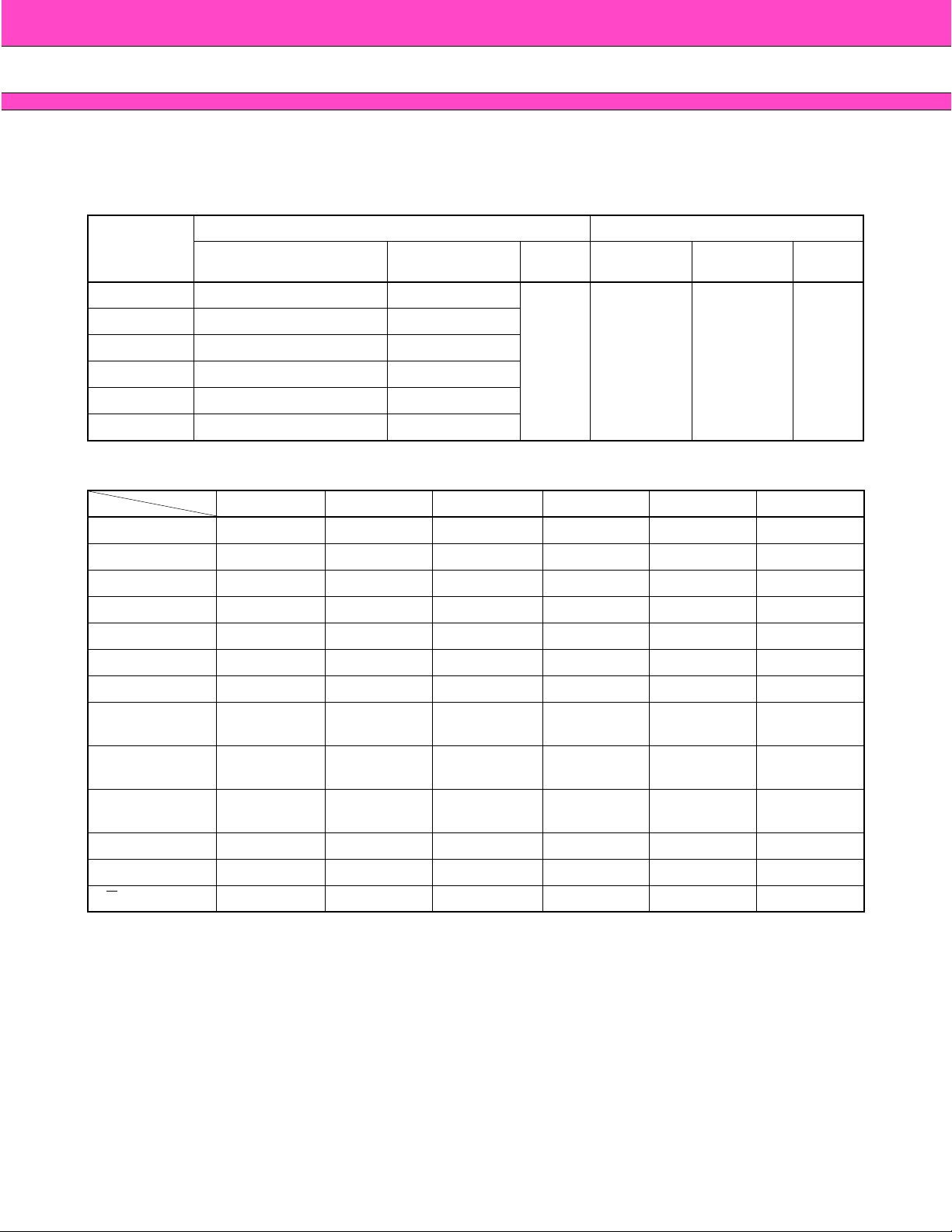
DESCRIPTION TABLE
Common Memory Attribute Memory
Part Number
Memory Device
MB98A81063 4M bit Flash Memory × 21M × 8/512K × 16
MB98A81183 8M bit Flash Memory × 22M × 8/1M × 16
Organization
(W × bit)
Access
Time
Memory
Device
To Top / Lineup / Index
Organization
(W × bit)
Access
Time
MB98A81273 16M bit Flash Memory × 24M × 8/2M × 16
MB98A81373 16M bit Flash Memory × 48M × 8/4M × 16
150 ns
max.
16K bit
EEPROM × 1
2K × 8
250 ns
max.
MB98A81473 16M bit Flash Memory × 816M × 8/8M × 16
MB98A81573 16M bit Flash Memory × 16 32M × 8/16M × 16
DIFFERENCES
MB98A81063 MB98A81183 MB98A81273 MB98A81373 MB98A81473 MB98A81573
Density 1MB 2MB 4MB 8MB 16MB 32MB
Memory Device 4M bit 8M bit 16M bit ←←←
Quantity 2224816
Read 1 B unit ←←←←←
Program 1 B unit ←←←←←
Chip Erase 512 KB unit 1 MB unit 2 MB unit ←←←
Sector Erase 64 KB unit ←←←←←
Number of
Sectors
Erase Suspend
Read
16 32 64 128 256 512
Yes Yes Yes Yes Yes Yes
Erase Suspend
Program
Address A
No Yes Yes Yes Yes Yes
to A
0
19
A0 to A
20
A0 to A
21
A0 to A
22
A0 to A
23
A0 to A
RESET No Yes Yes Yes Yes Yes
R/B No Yes Yes Yes Yes Yes
24
3
To Top / Lineup / Index
MB98A81063-15/81183-15/81273-15/81373-15/81473-15/81573-15
DESCRIPTIONS (Continued)
■
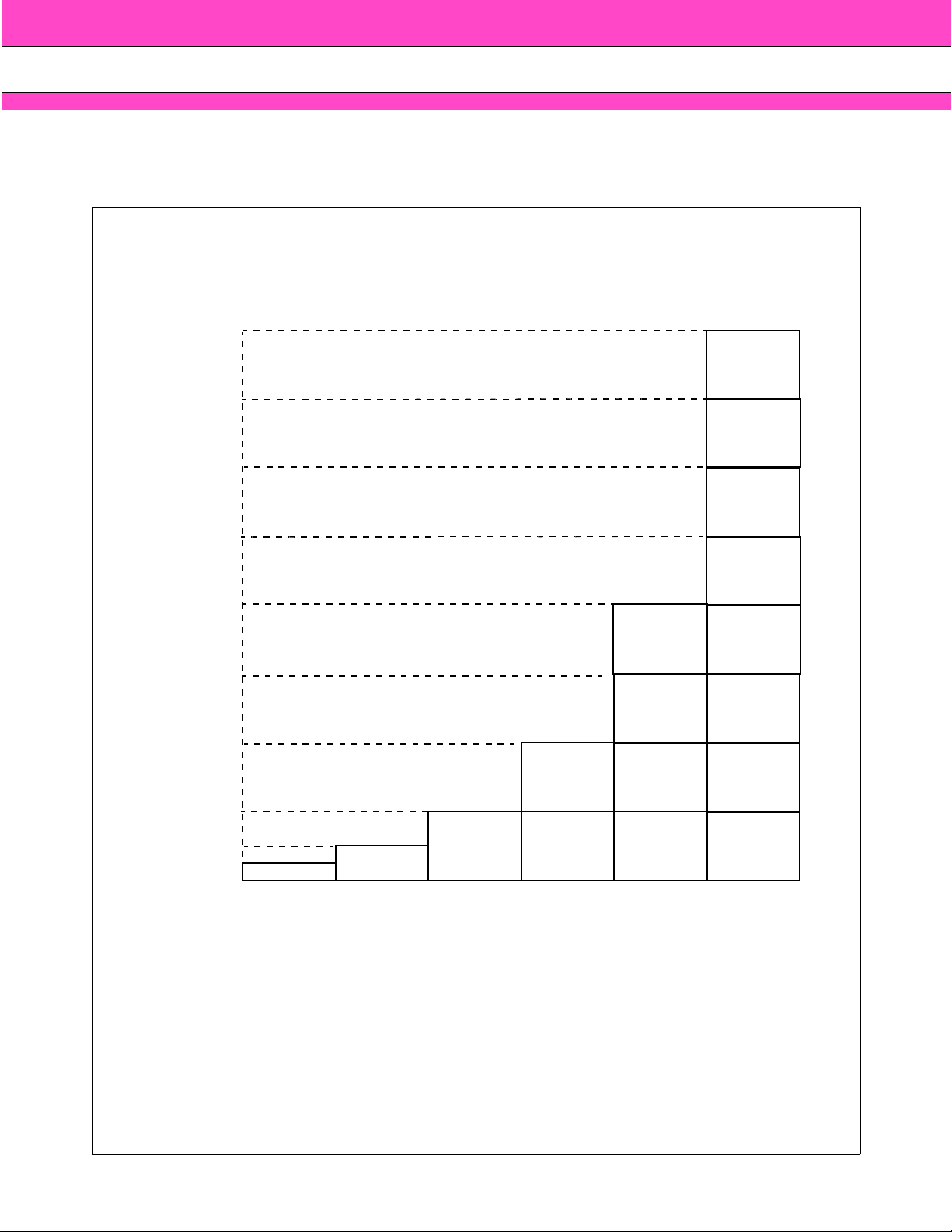
ADDRESS MAP (for × 16 mode, not contained A0)
FFFFFFh
DFFFFFh
BFFFFFh
chip15, 14
chip13, 12
9FFFFFh
7FFFFF
5FFFFFh
3FFFFFh
1FFFFFh
0FFFFFh
07FFFFh
000000h
chip11,10
chip9, 8
h
chip7, 6
chip5, 4
chip3, 2
chip1, 0
chip1, 0
MB98A81063MB98A81183 MB98A81273 MB98A81373 MB98A81473 MB98A81573
chip1, 0
chip1, 0
chip3, 2
chip1, 0
chip7, 6
chip5, 4
chip3, 2
chip1, 0
4
To Top / Lineup / Index
MB98A81063-15/81183-15/81273-15/81373-15/81473-15/81573-15
PIN ASSIGNMENTS
■
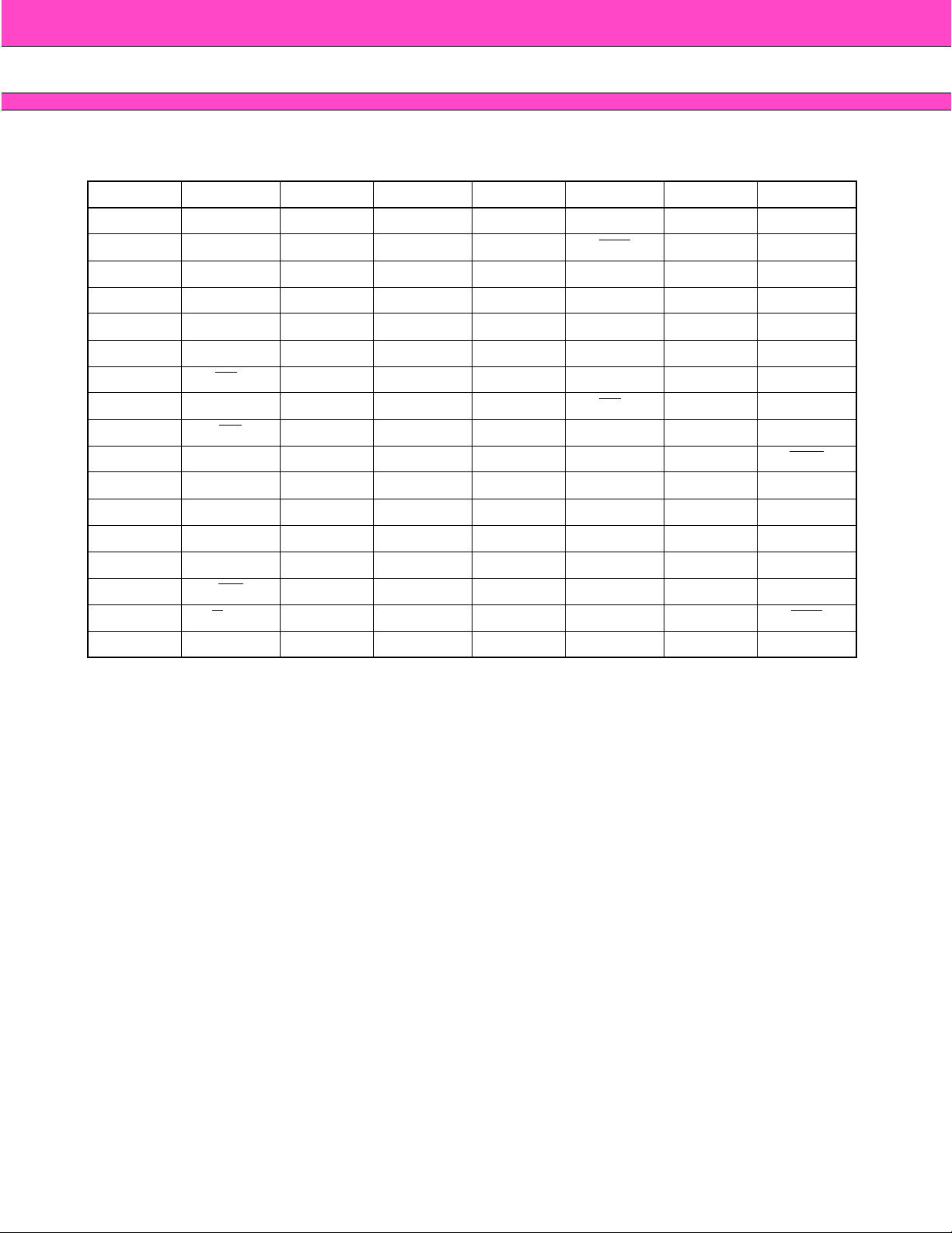
Pin No. Symbol Pin No. Symbol Pin No. Symbol Pin No. Symbol
1 GND 18 N.C. 35 GND 52 N.C.
2D
3
19 A
16
36 CD1 53 A22/N.C.*
3D
4D
5D
6D
7CE
8A
4
5
6
7
124 A541 D
10
9OE
10 A
11 A
12 A
13 A
14 A
11
9
8
13
14
15 WE 32 D
20 A
21 A
22 A
23 A
25 A
26 A
27 A
28 A
29 A
30 D
31 D
15
12
7
6
4
3
2
1
0
0
1
2
37 D
38 D
39 D
40 D
11
12
13
14
15
42 CE259N.C.
43 N.C. 60 N.C.
44 N.C. 61 REG
45 N.C. 62 BVD2
46 A
47 A
48 A
17
18
19
49 A20/N.C.* 66 D
54 A23/N.C.*
55 A24/N.C.*
56 N.C.
57 N.C.
58 RESET/N.C.
63 BVD1
64 D
65 D
16 R/B/N.C.* 33 WP 50 A21/N.C.* 67 CD2
17 V
CC
34 GND 51 V
CC
68 GND
* : See “DESCRIPTIONS”.
8
9
10
5
To Top / Lineup / Index
MB98A81063-15/81183-15/81273-15/81373-15/81473-15/81573-15
PIN DESCRIPTIONS
■
Symbol Pin Name Input/Output Function
A
to A
0
24
D
to D
0
15
CE
1 Card Enable for Lower Byte Input
CE
2 Card Enable for Upper Byte Input
REG
Address Input Input Address Inputs, A0 to A24.
Data Inputs/Outputs.
Data Input/Output Input/Output
This data bus size (8-bit or 16-bit) is selected with
CE
1 and CE2.
Active Low.
-Lower byte (D0 to D7) is selected for read/write/
erase function of flash memory cards.
Active Low.
-Upper byte (D8 to D15) is selected for read/write /
erase function of flash memory cards.
Active Low.
Attribute Memory Select Input
-Attribute memory is selected for read/write
function of identification data of flash memory
cards. (N.C. or “FF” data or attribute data.)
OE
WE
, CD2 Card Detect Output
CD1
Output Enable Input
Write Enable Input
Active Low.
-Output enable for flash memory cards.
Active Low.
-Write enable for flash memory cards.
These pins detect if the card has been correctly
inserted. Both pins are tied to GND internally.
Write controller for flash memory cards.
WP Write Protect Output
This pin outputs the Protect/Non Protect status of
“WP Switch”.
BVD1, BVD2 Battery Voltage Detect Output Both pins are tied to V
RESET Hardware Reset Input
R/B
V
CC
Ready/Busy Output
Power Supply — Power Supply Voltage. (+5.0 V ±5%)
The card may be reset by driving the RESET pin
to V
.
IH
System can be detect the completion of program
or erase operation.
GND Ground — System Ground.
N.C. Non Connection —
PIN LOCATIONS
■
Fig. 1 - BOTTOM VIEW (CONNECTOR SIDE)
CC
internally.
Front Side
34
68
Back Side
1
35
6
MB98A81063-15/81183-15/81273-15/81373-15/81473-15/81573-15
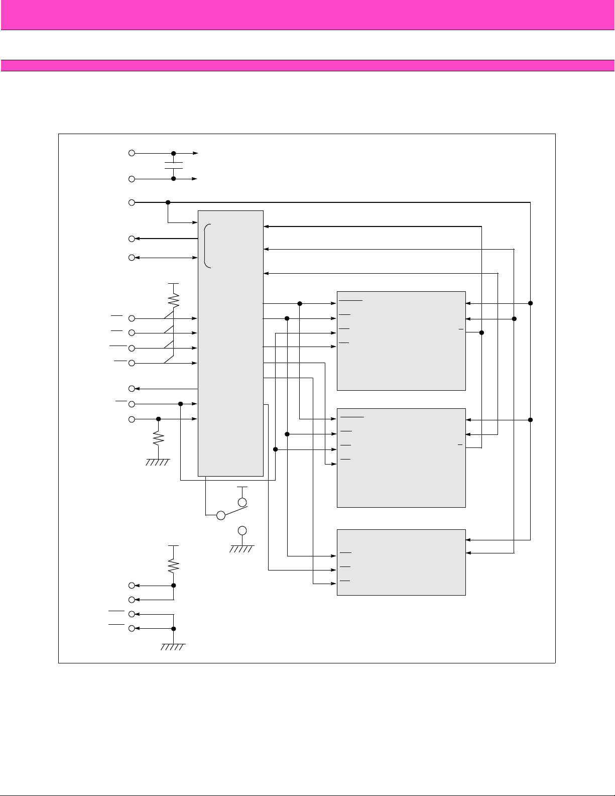
BLOCK DIAGRAM
■
MB98A81063, MB98A81183, MB98A81273 and MB98A81373
V
CC
Internal circuit
To Top / Lineup / Index
GND
Address
R/B*1
D0 to D
CE1
CE2
REG
WE
WP
OE
RESET*1
15
510 K
V
CC
100 K
Internal circuit
Buffer
I/O Buffer
Decoder
WP Control
V
CC
RESET
WE
OE
CE
RESET
WE
OE
CE
(EVEN BYTE)
4M Flash chip × 1 (81063)
8M Flash chip × 1 (81183)
16M Flash chip × 1 (81273)
16M Flash chip × 2 (81273
(ODD BYTE)
4M Flash chip × 1 (81063)
8M Flash chip × 1 (81183)
16M Flash chip × 1 (81273)
16M Flash chip × 2 (81373)
Address
I/O
R/B
Address
I/O
R/B
V
CC
10 K
BVD1
BVD2
CD1
CD2
*1: Not available for MB98A81063.
WP Switch
Fig. 2.1 - Block Diagram
WE
OE
CE
Attribute memory
16K EEPROM
Address
I/O
7
To Top / Lineup / Index
MB98A81063-15/81183-15/81273-15/81373-15/81473-15/81573-15
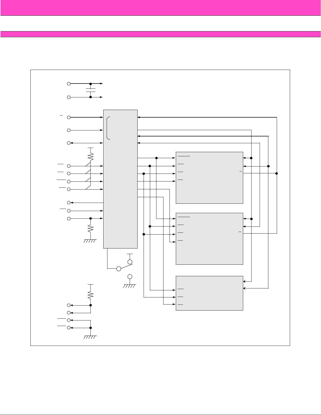
BLOCK DIAGRAM (Continued)
■
MB98A81473 and MB98A81573
V
CC
Internal circuit
GND
R/B
Address
D0 to D
CE1
CE2
REG
WE
RESET
15
WP
OE
V
100 K
510 K
Internal circuit
Control circuit
Buffer
I/O Buffer
Decoder
WP Control
CC
RESET
WE
OE
CE
RESET
WE
OE
CE
V
CC
(EVEN BYTE)
16M Flash chip × 4 (81473)
16M Flash chip × 8 (81573)
(ODD BYTE)
16M Flash chip × 4 (81473)
16M Flash chip × 8 (81573)
Address
I/O
R/B
Address
I/O
R/B
Address
I/O
BVD1
V
10 K
CC
WP Switch
WE
OE
CE
Attribute memory
16K EEPROM
BVD2
CD1
CD2
Fig. 2.2 - Block Diagram
8
To Top / Lineup / Index
MB98A81063-15/81183-15/81273-15/81373-15/81473-15/81573-15
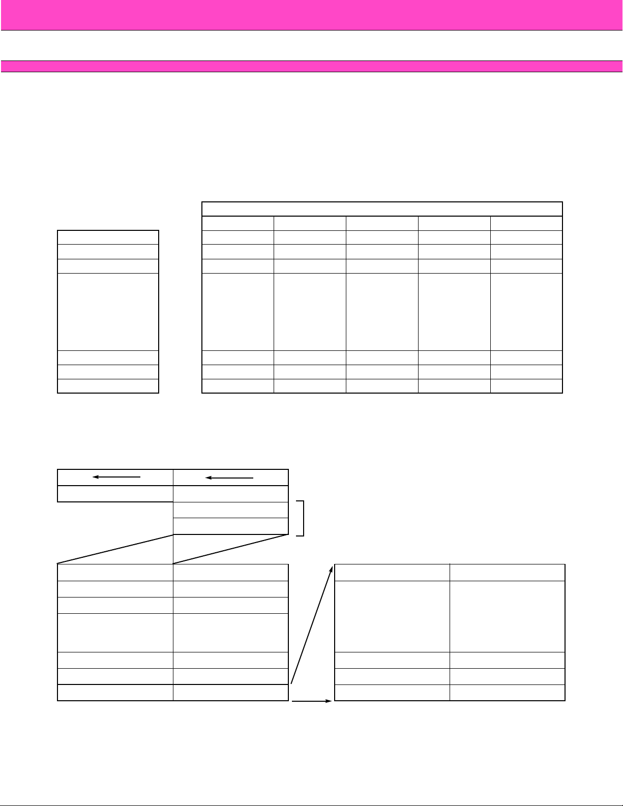
CHIP AND SECTOR DECODING
■
• Chip can be selected with;
- A
, A22, A23 and A24 for × 8-bit mode No.1.
0
- A
, A23 and A24 for × 8-bit mode No.2 and × 16-bit mode.
22
• Sector per each chip can be selected with A
ERASE SECTOR DECODING TABLE
A
*2 A20*1 A
21
Sector 31 1 1 1 1 1
Sector 30 1 1 1 1 0
Sector 29 1 1 1 0 1
•
•
•
Total 32 sectors*1*2
per 1 chip
•
•
•
Sector 2 0 0010
Sector 1 0 0 0 0 1
Sector 0 0 0000
•
•
•
•
•
, A18, A19, A20 and A21.
17
Sector Address (SA)
•
•
•
•
•
19
•
•
•
•
•
A
18
•
•
•
•
•
A
17
•
•
•
•
•
*1:A20 is not available for MB98A81063. MB98A81063 has 8 sectors.
*2:A
is not available for MB98A81063 and MB98A81183. MB98A81063 has 8
21
sectors and MB98A81183 has 16 sectors.
CARD CHIP / SECTOR CONFIGURATION
D
D
15
8
UPPER BYTE LOWER BYTE
Chip 15 Chip 14
Chip 13 Chip 12
Chip 11 Chip 10
•
•
•
Chip 5 Chip 4 Sector 2 (64K × 8 bits) Sector 2 (64K × 8 bits)
Chip 3 Chip 2 Sector 1 (64K × 8 bits) Sector 1 (64K × 8 bits)
Chip1 Chip 0
D7 D
EVEN ADDRESS BYTE
ODD ADDRESS BYTE
•
•
•
0
× 16 bit mode
× 8 bit mode No. 1
(16M Flash Chip
Sector 31
Sector 0 (64K × 8 bits) Sector 0 (64K × 8 bits)
Chip 1
*1
)
*2
(64K × 8 bits) Sector 31*2(64K × 8 bits)
•
•
•
•
•
•
Chip 0
(16M Flash Chip*1)
•
•
•
•
•
•
Card Chip Configuration for 32MB Card Sector Configuration for 2 Chips
*1:4M Flash Chip for MB98A81063. 8M Flash chip for
MB98A81183.
*2:Sector 7 for MB98A81063. Sector 15 for MB98A81183.
9

To Top / Lineup / Index
MB98A81063-15/81183-15/81273-15/81373-15/81473-15/81573-15
FUNCTION DESCRIPTIONS
■
1. Read Mode
The data in the common and attribute memory can be read with “OE=VIL” and “WE=VIH”. The address is selected
with A
The following 1) and 2) are the descriptions for Common Memory Read and Attribute Memory Read mode.
(1) Common Memory Read
(2) Attribute Memory Read
2. Standby Mode
3. Output Disable Mode
4. Write Mode
(1) Common Memory Wr ite
(2) Attribute Memory Write
5. Command Definitions
6. Automated Program Capability
7. Automated Chip Erase Capability
to A24. And CE1 and CE2 select output mode (× 8/× 16 output mode, See “FUNCTION TRUTH TABLES”.).
0
- Two modes of Common Memory Read, reading the data in memory array and Intelligent ID are available.
The card enter each Read mode by writing “Read Memory/Reset Command” or “Intelligent ID Read Command”.
The card automatically resets to the condition of Common Memory Read mode upon initial power-up.
- The data on the attribute memory can be read with “REG
- An address on attribute memory can be selected with A
-CE1 and CE2 at “VIH” place the card in Standby mode. D0 to D15 are placed in a high-Z state independent of
the status “OE
- The outputs are disabled with OE and WE at “VIH”. D0 to D15 are placed in high-Z state.
- The card is in Write mode with “OE
- Commands can be written at the Write mode. See “5.Command Definitions”.
- Two types of the Write mode, “WE
-REG
- Attribute memory is not controlled by writing Commands. And attribute memory has the Data polling function,
- User can select the card operation by writing the specific address and data sequences into the command
- Programming operation can swich the data from “1” to “0”.
- The data is programmed on a byte-by-byte or word-by-word basis.
- The card will automatically provide adequate internally generated programming pulses and verify the
- Addresses are latched at falling edge of WE
- We can check whether a byte (word) progr amming operation is completed successfully b y sequence flug with
- Any commands written to the chip during programming operation will be ignored.
- We can execute chip erase operation by 6 bus cycle operation. Chip erase does not require the user to pre-
- The card returns to Common Memory Read mode automatically after the chip erasing is completed.
at L-level selects Attrib ute memory and “OE=VIH”, “WE and CE=VIL” place it in write mode. Two types of
the write mode, “WE
which can detect whether the attribute memory status is in programming operation. When the read operation
is executed at programming cycle, the opposite data is output from D
written data is output from D
register. If incollect address and data are written or improper sequence is done, the card is reseted to read
mode. See “COMMAND DEFINISION TABLE”.
programmed cell margine by writing four bus cycle operation. The card returns to Common Memory Read
mode automatically after the programming is completed.
rising edge of WE or CE on the command write cycle begins programming operation.
R/B
(Except for MB98A81063), Data Polling or Toggle Bit function. See “WRITE OPERATION STATUS”.
program prior to erase. Upon executing the Erase command sequence the chip automatically will program
and verify the entire memory for an all zero data pattern prior to electrical erase. The system is not required
to provide any controls or timing during these operations.
”, “WE” and “REG”.
=VIH” and “WE and CE=VIL”.
control” and “CE control” are available.
control” and “CE control” are available.
pin at the completion of programming operation.
7
or CE and data is latched at rising edge of WE or CE. The fourth
=VIL”, “OE=VIL” and “WE=VIH”.
to A11 pin. And CE1 and CE2 select output mode.
0
(I7), and the same data (O7) as the
7
10
To Top / Lineup / Index
MB98A81063-15/81183-15/81273-15/81373-15/81473-15/81573-15
FUNCTION DESCRIPTIONS (Continued)
■
- Whether or not chip erase operation is completed successfully can be checked by sequence flug with R/B
(Except for MB98A81063), Data
- Any commands written to the chip during programming operation will be ignored.
8. Automated Sector Erase Capability
- We can execute the erase operation on any sectors by 6 bus cycle operation.
- A time-out of 50 µs (typ.) from the rising edge of the last Sector Erase command will initiate the Sector Erase
command(s) for other sector than the sector that sector erase command have been valid.
- Multiple sectors in a chip can be erased concurrently . This sequence is followed with writes of 30H to addresses
in other sectors desired to be concurrently erased. The time between writes 30H must be less than 50 µs,
otherwise that command will not be accepted. Any command other than Sector Erase or Erase Suspend during
this time-out period will reset the chip to Read mode. The automated sector erase begins after the 50 µs (typ.)
time out from the rising edge of WE
window is still open can be monitored with D
- Sector Erase does not require the user to pre-program prior to erase. The chip automatically programs “0” to
all memory locations in the sector(s) prior to electrical erase. The system is not required to provide any controls
or timing during these operations.
- The card returns to Common Memory Read mode automatically after the sector erasing is completed.
- Whether or not sector erase operation is completed successfully can be checked by sequence flug with R/B
Data Polling or Toggle Bit function. The sequence flug must be read from the address of the sector inv olv ed in
erase operation. See “WRITE OPERATION STATUS”.
9. Erase Suspend
- Erase Suspend command allows the user to interrupt the sector erase operation and then do data reads or
program from or to a non-busy sector in the chip which has the sector(s) suspended erase (only data read is
possible for MB98A81063). This command is applicab le only during the sector erase oper ation (including the
sector erase time-out period after the sector erase commands 30H) and will be ignored if written during the
chip erase or programming operation. Writing this command during the time-out will result in immediate
termination of the time-out period. The addresses are “don’t cares” in wrinting the Erase Suspend or Resume
commands in the chip.
- When the Erase Suspend command is written during a Sector Erase operation, the chip will enter the Erase
Suspend Read mode. User can read the data from other sectors than those in suspention. The read operation
from sectors in suspention results D
non-busy sectors by writing program commands for MB98A81183 and MB98A8xx7x.
- A read from a sector being erase suspended may result in invalid data.
10. Intelligent Identifier (ID) Read Mode
- Each common memory can execute an Intelligent Identifier oper ation, initiated by writing Intelligent ID command
(90H). Following the command write, a read cycle from address 00H retrieves the manufacture code, and a
read cycle from address 01H returns the device code as follows. To terminate the operation, it is necessary
to write Read/Reset command.
Part Number Maker Code Device Code
MB98A81063 04 h / 0404 h A4 h / A4A4 h
MB98A81183 04 h / 0404 h D5 h / D5D5 h
MB98A81273/81373/1473/81573 04 h / 0404 h 3D h / 3D3D h
Polling or Toggle Bit function. See “WRITE OPERATION STATUS”.
pulse for the last Sector Erase command pulse. Whether the sector er ase
and D11.
3
toggling for MB98A81183 and MB98A8xx7x. User can program to
2/D10
,
11. Hardware Reset (not applied for MB98A81063)
- The Card may be reset by driving the RESET pin to VIH. The RESET pin must be kept High (VIH) for at least
500 ns. Any operation in progress will be terminated and the card will be reset to the read mode 20 µs after
the RESET pin is driven High. If a hardware reset occurs during a program operation, the data at that particular
location will be indeterminate.
- When the RESET pin is high and the internal reset is complete, the Card goes to standby mode and cannot
be accessed. Also, note that all the data output pins are High-Z for the duration of the RESET pulse. Once
the RESET pin is taken low, the Card requires 500 ns of wake up time until outputs are valid for read access.
- If hardware reset occurs during a erase operation, there is a possibility that the erasing sector(s) cannot be
used after this.
11
To Top Lineup Index//
MB98A81063-15/81183-15/81273-15/81373-15/81473-15/81573-15
FUNCTION DESCRIPTIONS (Continued)
■
12. Data Protection
- The card has WP (Write Protect) switch for write lockout.
- T o a void initiation of a write cycle during V
than 3.2 V (typically 3.7 V). If V
CC
< V
circuits are disabled. Under this condition the device will reset to the read mode. Subsequent writes will be
ignored until the V
level is greater than V
CC
logically correct to prevent unintentional writes when V
-If V
would be less than V
CC
operation will not resume ev en if V
during program/erase operation, the operation will stop. And after that, the
LKO
returns recommended voltage level. Theref ore, prog ram command must
CC
be written again because the data on the address interrupted program operation is invalid. And regarding
interrupting erase operation, there is possibility that the erasing sector(s) cannot be used.
- Noise pulses of less than 5 ns (typical) on OE
FUNCTION TRUTH TABLE
■
MAIN MEMORY FUNCTION*1
power-up and power-do wn, a write cycle is locked out f or VCC less
CC
, the command register is disabled and all internal program/erase
LKO
It is the users responsibility to ensure that the control pins are
LKO.
is above 3.2 V.
CC
, CE or WE will not initiate a write cycle.
Mode RESET*3 REG
CE2CE1A0OE WE
WP
*2
Data Input/Output
D8 to D
D0 to D
15
WP SW
7
Hardware Reset H XXXXXXX High-Z
Standby
Read (×8 No.1)
Read (×8 No.1) H
Read (×8 No.2)
Read (×16) L D
Write (×8 No.1)
Output Disable H High-Z P
L
Write (×8 No.1)
Output Disable H
Write (×8 No.2)
Output Disable H High-Z P
Write (×16)
XHHXXXX High-Z
OUT
D
(Even Byte)
OUT
D
(Odd Byte)
High-Z
OUT
D
(Even Byte)
HL
H
L
L
LHX
X
L
L
High-Z
OUT
D
(Odd Byte)
H
HL
L
H
High-Z
D
(Odd Byte)
HL
IN
H
L
L
X
D
(Odd Byte)
LD
High-Z
IN
P or NP
IN
IN
L
Output Disable H High-Z P
NP
NP
P
NP
NP
Output Disable XXXXHHX High-Z P or NP
Notes:
*1:H =V
, L = VIL, X = Either VIL or VIH, WP SW = Write Protect Switch, P = Protect, NP = Non Protect
IH
*2:L-level is output when WPSW = NP. H-level is output when WPSW = P.
*3:Not available for MB98A81063.
12
MB98A81063-15/81183-15/81273-15/81373-15/81473-15/81573-15
FUNCTION TRUTH TABLE (Continued)
■
ATTRIBUTE MEMORY FUNCTION*1
To Top Lineup Index//
Mode RESET*3 REG
Standby
Read (×8 No.1)
CE2CE1A0OE WE
XHHXXXX High-Z
L
WP
*2
HL
Read (×8 No.1) H H
Data Input/Output
D8 to D
D0 to D
15
High-Z
WP SW
7
OUT
D
P or NP
LHX
Read (×8 No.2)
Read (×16) L D
Write (×8 No.1)
H
L
XH
L
High-Z
OUT
IN
D
NP
L
Output Disable H High-Z P
Write (×8 No.1)
HL
L
L
H
L
High-Z
INVALID
IN
D
NP
Output Disable H
Write (×8 No.2)
HL
H
L
INVALID
IN
D
High-Z
NP
Output Disable H High-Z P
L
Write (×16)
X
L
L
INVALID
IN
D
D
IN
NP
Output Disable H High-Z P
P
Output Disable XXXXHHX High-Z P or NP
Notes:
*1:H = V
, L = VIL, X = Either VIL or VIH, WP SW = Write Protect Switch, P = Protect, NP = Non Protect
IH
*2:L-level is output when WPSW = NP. H-level is output when WPSW = P.
*3:Not available for MB98A81063.
13
To Top / Lineup / Index
MB98A81063-15/81183-15/81273-15/81373-15/81473-15/81573-15
COMMAND DEFINITION TABLE
■
Command table for 8-bit Mode
Command
Read/Reset 1 2
Read/Reset 2 4
Read
Intelligent
ID Codes
Byte Program 4
Sector Erase 6
Chip Erase 6
Sector Erase
Suspend
Sector Erase
Resume
Bus
Cycle
1st Bus
Write Cycle
Write Read
CA F0H RA RD
Write Write Write Read
RCMA1 AAH RCMA2 55H RCMA1 F0H RA RD
Write Write Write Read
4
ICMA1 AAH ICMA2 55H ICMA1 90H IA ID
Write Write Write Write
PCMA1 AAH PCMA2 55H PCMA1 A0H PA PD
Write Write Write Write Write Write
SCMA1 AAH SCMA2 55H SCMA1 80H SCMA1 AAH SCMA2 55H SA 30H
Write Write Write Write Write Write
CCMA1 AAH CCMA2 55H CCMA1 80H CCMA1 AAH CCMA2 55H CCMA1 10H
Write
1
CA B0H
Write
1
CA 30H
2nd Bus
Write/Read
Cycle
3rd Bus Write
Cycle
4th Bus
Write/Read
Cycle
5th Bus Write
Cycle
6th Bus Write
Cycle
Notes:
CA: Chip Address. (address in chip selected by A
SA: Sector Address (address in 64 KB selected by A
PA: Program Address (address to be programmed)
RA: Read Address (address to be read)
IA: Intelligent ID read address (Manufacture Code 0000H, Device Code 0002H)
PD: Programming data
RD: Read data
ID: Intelligent Identifier (ID) Code
CCMA1, CCMA2: Command adddress for chip erase
SCMA1, SCMA2: Command address for sector erase
PCMA1, PCMA2: Command address for program
RCMA1, RCMA2: Command address for Read/Reset
ICMA1, ICMA2: Command address for intelligent ID read
14
, A22, A23 and A24)
0
, A17, A18, A19, A20, A21, A22, A23 and A24)
0
See “Command Address Table for
8-bit Mode” in page 16.
MB98A81063-15/81183-15/81273-15/81373-15/81473-15/81573-15
Command Table for 16-bit Mode*1
To Top / Lineup / Index
Command
Bus
Cycle
Read/Reset 1 2
Read/Reset 2 4
Read
Intelligent
ID Codes
Byte Program 4
Sector Erase 6
Chip Erase 6
Sector Erase
Suspend
Sector Erase
Resume
1st Bus
Write Cycle
Write Read
— F0F0H RA RD
Write Write Write Read
RCMA1 AAAAH RCMA2 5555H RCMA1 F0F0H RA RD
Write Write Write Read
4
ICMA1 AAAAH ICMA2 5555H ICMA1 9090H IA ID
WriteWriteWriteWrite
PCMA1 AAAAH PCMA2 5555H PCMA1 A0A0H PA PD
WriteWriteWriteWriteWriteWrite
SCMA1 AAAAH SCMA2 5555H SCMA1 8080H SCMA1 AAAAH SCMA2 5555H SA 3030H
WriteWriteWriteWriteWriteWrite
CCMA1 AAAAH CCMA2 5555H CCMA1 8080H CCMA1 AAAAH CCMA2 5555H CCMA1 1010H
1
1
Write
CA B0B0H
Write
CA 3030H
2nd Bus
Write/Read
Cycle
3rd Bus
Write Cycle
4th Bus
Write/Read
Cycle
5th Bus
Write Cycle
Write Cycle
6th Bus
Notes:
CA: Chip Address. (address in chip selected by A
SA: Sector Address (address in 128 KB selected by A
, A23 and A24)
22
, A18, A19, A20, A21, A22, A23 and A24)
17
PA: Program Address (address to be programmed)
RA: Read Address (address to be read)
IA: Intelligent ID read address (Manufacture Code 0000H, Device Code 0001H)
PD: Programming data
RD: Read data
ID: Intelligent Identifier (ID) Code
CCMA1, CCMA2: Command address for chip erase
SCMA1, SCMA2: Command address for sector erase
PCMA1, PCMA2: Command address for program
RCMA1, RCMA2: Command address for Read/Reset
See “Command Address Table for
16-bit Mode” in page 16.
ICMA1, ICMA2: Command address for intelligent ID read
*1: Address number is not contained “A
”.
0
15
To Top / Lineup / Index
MB98A81063-15/81183-15/81273-15/81373-15/81473-15/81573-15
COMMAND DEFINITION TABLE (Continued)
■
Command Address Table for 8-bit Mode
Command
Address
CCMA1 (CA AND 000001h) OR AAAAh (CA AND 000001h) OR AAAh CA
CCMA2 (CA AND 000001h) OR 5554h (CA AND 000001h) OR 554h CA
SCMA1 (SA AND 000001h) OR AAAAh (SA AND 000001h) OR AAAh CA
SCMA2 (SA AND 000001h) OR 5554h (SA AND 000001h) OR 554h CA
PCMA1 (PA AND 000001h) OR AAAAh (PA AND 000001h) OR AAAh CA
PCMA2 (PA AND 000001h) OR 5554h (PA AND 000001h) OR 554h CA
RCMA1 (RA AND 000001h) OR AAAAh (RA AND 000001h) OR AAAh CA
RCMA2 (RA AND 000001h) OR 5554h (RA AND 000001h) OR 554h CA
ICMA1 (IA AND 000001h) OR AAAAh (IA AND 000001h) OR AAAh CA
ICMA1 (IA AND 000001h) OR 5554h (IA AND 000001h) OR 554h CA
MB98A81063 MB98A81183
MB98A81273, 81373, 81473,
Command Address Table for 16-bit Mode
Command
Address
CCMA1 5555h 555h CA
CCMA2 2AAAh 2AAh CA
SCMA1 5555h 555h CA
MB98A81063 MB98A81183
MB98A81273, 81373, 81473,
81573
81573
SCMA2 2AAAh 2AAh CA
PCMA1 5555h 555h CA
PCMA2 2AAAh 2AAh CA
RCMA1 5555h 555h CA
RCMA2 2AAAh 2AAh CA
ICMA1 5555h 555h CA
ICMA1 2AAAh 2AAh CA
16

MB98A81063-15/81183-15/81273-15/81373-15/81473-15/81573-15
WRITE OPERATION STATUS
■
Hardware Sequence Flag Table
To Top / Lineup / Index
Status D
Programming D
7
7
, D
, D
D6, D
15
Toggle0010
15
D5, D
14
13
D3, D
D2, D10*4 R/B*4
11
Erasing 0 Toggle 0 1 Toggle 0
In
Progress
Exceeded
Time
Limits
Erase
Suspend
Read
Erase Suspend*4
Program
Programming D
Erasing 0 Toggle 1 1 N/A 0
Erase Suspend*4
Program
(1)11 00*11
(2)DataDataDataDataData 1
, D
D
7
15
, D
7
15
D
, D
7
15
*2 0 0 *1, *3 0
Toggle1010
Toggle 1 0 N/A 0
Notes:
(1): Erase Suspended Sector (2): Non-Erase Suspended Sector
*1. Performing successive read operations from the erase-suspended sector will cause D
*2. Performing successive read operations from any address will cause D
, D14 to toggle.
6
, D10 to toggle.
2
*3. Reading the byte address being programmed while in the erase-suspend program mode will indicate logic
“1” at the D
, D10 bit. However, successive reads from the erase-suspended sector will cause D2, D10 to
2
toggle.
*4. Not applied for MB98A81063.
D7, D15 (Data Polling)
The card features Data Polling as a method to indicate to the host that the Program/Erase Operation are in
progress or completed. During the program operation an attempt to read the program address will produce the
compliment of the data last written to D
program address will produce the true data last written to D
read the erase address will produce a “0” at the D
attempt to read the device will produce a “1” at the D
For Chip Erase, the Data
Polling is v alid after the rising edge of the sixth WE pulse in the six write pulse sequence.
. Upon completion of the program operation, an attempt to read the
7/D15
. During the erase operation, an attempt to
7/D15
output. Upon completion of the erase operation an
7/D15
output.
7/D15
For sector erase, the Data Polling is valid after the last rising edge of the sector erase WE pulse. Even if the
device has completed the operation and D
still invalid. The valid data on D
to D7/D8 to D15 will be read on the successive read attempts.
0
has a valid data, the data outputs on D0 to D6/D8 to D14 may be
7/D15
The Data Polling feature is only active during the programming operation, erase operation, sector erase timeout, Erase Suspend Read mode and Erase Suspend Program mode.
D6, D14 (Toggle Bit l)
The card also features the “Toggle Bit” as a method to indicate to the host system that the Program/Erase
Operation are in progress or completed.
During an Program or Erase cycle, successive attempts to read (OE
result in D
toggling between one and zero . Once the Program or Erase cycle is completed, D6/D14 will stop
6/D14
toggling and valid data will be read on the next successive attempts. During programming, the Toggle Bit is
valid after the rising edge of the fourth WE
Bit is valid after the rising edge of the sixth WE
pulse in the four write pulse sequence. For chip erase, the Toggle
pulse in the six write pulse sequence. For sector erase, the
Toggle Bit is valid after the last rising edge of the sector erase WE
the sector time out.
Either CE
or OE toggling will cause the D6/D14 to toggle.
or CE toggling) data from the card will
pulse. The Toggle Bit is also active during
17

To Top / Lineup / Index
MB98A81063-15/81183-15/81273-15/81373-15/81473-15/81573-15
D5, D13 (Exceeded Timing Limits)
D5/D13 will indicate if the program or erase time has e xceeded the specified limits (internal pulse count). Under
these conditions D
cycle was not successfully completed. Data
If this failure condition occurs during sector erase operation, it specifies that a particular sector is bad and it
may not be reused, howe ver , other sectors are still functional and may be used for the program or erase oper ation.
The chip must be reset to use other sectors. Write the Reset command sequence to the chip, and then
execute Program or Erase command sequence. This allows the system to continue to use the other active
sectors in the chip.
If this failure condition occurs during the chip erase operation, it specifies that the entire chip is bad or
combination of sectors are bad.
If this failure condition occurs during the byte programming oper ation, it specifies that the entire sector containing
that byte is bad and this sector may not be reused, (other sectors are still functional and can be reused).
The D
failure condition ma y also appear if a user tries to program a non b lank location without er asing. In
5/D13
this case the card locks out and never completes the card operation. Hence, the system never reads a valid
data on D
bit and D6/D14 never stops toggling. Once the card has e xceeded timing limits , the D5/D13 bit will
7/D15
indicate a “1”. Please note that this is not a device failure condition since the device was incorrectly used.
will produce a “1”. This is a failure condition which indicates that the program or erase
5/D13
Polling is the only operating function of the card under this condition.
D3, D11 (Sector Erase Timer)
After the completion of the initial sector erase command sequence the sector erase time-out will begin. D3/D11
will remain low until the time-out is complete. Data
Polling and Toggle Bit are valid after the initial sector er ase
command sequence.
If Data
Polling or the Toggle Bit indicates the card has been written with a valid erase command, D3/D11 may
be used to determine if the sector erase timer window is still open. If D
is high (“1”) the internally controlled
3/D11
erase cycle has begun; attempts to write subsequent commands to the card will be ignored until the erase
operation is completed as indicated by Data
Polling or Toggle Bit. If D3/D11 is low (“0”), the card will accept
additional sector erase commands. To insure the command has been accepted, the system software should
check the status of D
prior to and following each subsequent sector erase command. If D3/D11 were high
3/D11
on the second status check, the command may not have been accepted.
Refer to Table : Hardware Sequence Flags.
D2, D10 (Toggle Bit ll, not applied for MB98A81063)
This Toggle bit, along with D6, can be used to determine whether the card is in the Erase operation or in Erase
Suspend.
Successive reads from the erasing sector will cause D
erase-suspended-read mode, successive reads from the er ase-suspended sector will cause D
to toggle during the Erase operation. If the card is in the
2
to toggle. When
2
the card is in the erase-suspended-program mode, successive reads from the byte address of the non-erase
suspended sector will indicate a logic ‘1‘ at the D
D
is different from D2 in that D6 toggles only when the standard Program or Erase, or Erase Suspend Prog ram
6
bit.
2
operation is in progress.
R/B (Ready/Busy, not applied for MB98A81063)
The card provides a R/B output pin as a way to indicate to the system that the program or erase operation are
either in progress or has been completed. If the output is low, the card is busy with either a program or erase
operation. If the card is placed in an Erase Suspend mode, the R/B
output will be high.
During programming, the R/B pin is driven low after the rising edge of the fourth WE pulse. During an erase
operation, the R/B
pin is driven low after the rising edge of the sixth WE pulse. The R/B pin will indicate a busy
condition during the RESET pulse.
18

MB98A81063-15/81183-15/81273-15/81373-15/81473-15/81573-15
PROGRAM / ERASE FLOWCHART
■
Fig. 3 - PROGRAM FLOWCHART
To Top / Lineup / Index
START
SET PA
SET ADDRESS
PCMA1,PCMA2*2
WRITE COMMAND
(PCMA1/AAH or AAAAH)*2
INCREMENT PA
WRITE COMMAND
(PCMA2/55H or 5555H)*2
WRITE COMMAND
(PCMA1/A0H/A0A0H)*2
WRITE DATA (PA/PD)
DA TA POLLING or
TOGGLE BIT *1
NO
LAST ADDRESS ?
YES
COMPLETED
*1 See Fig. 7, 6, 9, 10.
*2 See “COMMAND DEFINITION TABLE”.
Notes:
PD : PROGRAM DATA
PA : PROGRAM ADDRESS
19

To Top / Lineup / Index
MB98A81063-15/81183-15/81273-15/81373-15/81473-15/81573-15
PROGRAM / ERASE FLOWCHART (Continued)
■
Fig. 4 - CHIP ERASE FLOWCHART
START
SET CA
SET ADDRESS
(CCMA1,CCMA2)*2
WRITE COMMAND
(CCMA1/AAH or AAAAH)*2
INCREMENT CA
WRITE COMMAND
(CCMA2/55H or 5555H)*2
WRITE COMMAND
(CCMA1/80H or 8080H)*2
WRITE COMMAND
(CCMA1/AAH or AAAAH)*2
WRITE COMMAND
(CCMA2/55H or 5555H)*2
WRITE COMMAND
(CCMA1/10H or 1010H)*2
DA TA POLLING or TOGGLE BIT *1
YES
DESIRED OTHER
CHIPS ERASE ?
NO
COMPLETED
20
*1 See Fig. 7, 8, 9, 10.
*2 See “COMMAND DEFINITION TABLE”.
Note:
CA : CHIP ADDRESS

MB98A81063-15/81183-15/81273-15/81373-15/81473-15/81573-15
PROGRAM / ERASE FLOWCHART (Continued)
■
Fig. 5 - SECTOR ERASE FLOWCHART
START
SET SA
SET ADDRESS SCMA1,SCMA2*3
WRITE COMMAND
(SCMA1/AAH or AAAAH)*3
To Top / Lineup / Index
WRITE COMMAND
(SCMA2/55H or 5555H)*3
WRITE COMMAND
(SCMA1/80H or 8080H)*3
WRITE COMMAND
(SCMA1/AAH or AAAAH)*3
WRITE COMMAND
(SCMA2/55H or 5555H)*3
WRITE COMMAND
(SA/30H or 3030H)
DESIRED OTHER
SECTORS ERASE ?
DA TA
POLLING or TOGGLE BIT *1
*2
NO
COMPLETED
YES
WRITE COMMAND
(SA/30H or 3030H)
*1 See Fig.7, 8, 9, 10.
*2 Possible for the sectors in a chip
*3 See “COMMAND DEFINITION TABLE”.
Note:
SA : SECTOR ADDRESS
21

To Top / Lineup / Index
MB98A81063-15/81183-15/81273-15/81373-15/81473-15/81573-15
PROGRAM / ERASE FLOWCHART (Continued)
■
Fig. 6 - ERASE SUSPEND FLOWCHART
EXECUTING
SECTOR ERASE
WRITE COMMAND
(CA/B0H or B0B0H)
READ DATA (SA)*1
Yes
No
*1 Detection whether suspend mode is valid
can be done by Data
also. (MB98A81063 does not have R/B
*2 Only Read operation for MB98A81063.
Toggle
bit=Toggle?*1
No
Read or Program*2
STOP Erase
Suspend mode?
Yes
WRITE COMMAND
(CA/30H or 3030H)
FINISHED
Polling and R/B
).
22
Notes:
CA: CHIP ADDRESS
SA: SECTOR ADDRESS
RA: READ ADDRESS

To Top / Lineup / Index
MB98A81063-15/81183-15/81273-15/81373-15/81473-15/81573-15
PROGRAM / ERASE FLOWCHART (Continued)
■
Fig. 7 - DATA POLLING FLOWCHART: × 8-bit mode No.1
START
TIMER START *1
READ (VA) *2
D7=Data?
No
5
=1 or Time-up?
D
READ (VA) *2
Yes
No
Yes
D7=Data?
No
ERROR
*1 User sets the time period referring to
“PROGRAM AND ERASE PERFORMANCES”.
*2 ProgramVA=PA
Chip EraseVA=CA
Sector EraseVA=SA
Yes
COMPLETED
23

To Top / Lineup / Index
MB98A81063-15/81183-15/81273-15/81373-15/81473-15/81573-15
PROGRAM / ERASE FLOWCHART (Continued)
■
Fig. 8 - TOGGLE BIT FLOWCHART: × 8-bit mode No.1
START
TIMER START *1
READ (VA) *2
D6=Toggle?
Yes
No
*1 User sets the time period referring to
“PROGRAM AND ERASE PERFORMANCES”.
*2 Program VA=PA
Chip Erase VA=CA
Sector EraseVA=SA
5
=1 or Time-up?
D
READ (VA) *2
D6=Toggle?
Yes
ERROR
Yes
No
No
COMPLETED
24

MB98A81063-15/81183-15/81273-15/81373-15/81473-15/81573-15
PROGRAM / ERASE FLOWCHART (Continued)
■
Fig. 9 - DATA POLLING FLOWCHART: × 16-bit mode
START
To Top / Lineup / Index
No
EF=0
TIMER START *1
READ (VA) *2
7
=Data?
D
No
5
=1 or Time-up?
D
Yes
READ (VA) *2
7
D
=Data?
No
EF=1
Yes
Yes
*1 User sets the time period referring to
“PROGRAM AND ERASE PERFORMANCES”.
*2 Program VA=PA
Chip Erase VA=CA
Sector EraseVA=SA
Notes:
EF: Error Flag
EF=0: Operation Completed
EF=1: Lower Byte Error
EF=2: Upper Byte Error
EF=3: Lower/Upper Byte Error
1
READ (VA) *1
15
D
=Data?
No
Yes
1
No
13
D
=1 or Time-up?
Yes
READ (VA)
Yes
15
D
=Data?
No
EF=EF+2
EF=0?
No
Yes
COMPLETED
ERROR
25

To Top / Lineup / Index
MB98A81063-15/81183-15/81273-15/81373-15/81473-15/81573-15
PROGRAM / ERASE FLOWCHART (Continued)
■
Fig. 10 - TOGGLE BIT FLOWCHART: × 16-bit mode
START
No
EF=0
TIMER START *1
READ (VA) *2
D6=Toggle?
Yes
D5=1 or Time-up?
Yes
READ (VA)
D6=Toggle?
Yes
EF=1
No
No
*1 User sets the time period referring to
“PROGRAM AND ERASE PERFORMANCES”.
*2 Program VA=PA
Chip Erase VA=CA
Sector EraseVA=SA
Notes:
EF: Error Flag
EF=0: Operation Completed
EF=1: Lower Byte Error
EF=2: Upper Byte Error
EF=3: Lower/Upper Byte Error
1
READ (VA) *1
No
D14=Toggle?
Yes
26
1
No
D13=1 or Time-up?
Yes
READ (VA)
D14=Toggle?
Yes
EF=EF+2
EF=0?
Yes
COMPLETED
No
No
ERROR

MB98A81063-15/81183-15/81273-15/81373-15/81473-15/81573-15
ABSOLUTE MAXIMUM RATINGS (See WARNING)
■
Parameter Symbol Value Unit
To Top / Lineup / Index
Temperature under Bias T
Storage Temperature T
WARNING:
Supply Voltage V
Input Voltage V
Output Voltage V
CC
IN
OUT
A
STG
Semiconductor devices can be permanently damaged by application of stress (voltage, current,
–0.5 to +6.0 V
–0.5 to VCC +0.5 V
–0.5 to VCC +0.5 V
0 to +60 °C
–30 to +70 °C
temperature, etc.) in excess of absolute maximum ratings. Do not exceed these ratings.
RECOMMENDED OPERATING CONDITIONS
■
(Referenced to VSS)
Parameter Symbol Min. Typ. Max. Unit
V
Supply Voltage V
CC
CC
Ground GND — 0 — V
Ambient Temperature T
WARNING:
The recommended operating conditions are required in order to ensure the normal operation of the
A
semiconductor device. All of the device’s electrical characteristics are warranted when the device is
operated within these ranges.
Always use semiconductor devices within their recommended operating conditions ranges Operation
outside these ranges may adversely affect reliability and could result in device failure.
No warranty is made with respect to uses, operating conditions, or combinations not represented on
the data sheet. Users considering application outside the listed conditions are advised to contact their
FUJITSU representatives beforehand.
4.75 5.0 5.25 V
0—55°C
CAPACITANCE
■
Parameter Symbol Min. Max. Unit
Input Capacitance *1 C
I/O Capacitance *2 C
IN
I/O
Notes:
*1 This value does not apply to CE
1, CE2, WE, REG and RESET.
*2 This value does not apply to CD1, CD2, BVD1 and BVD2.
(TA = 25°C, f = 1 MHz, VIN = V
= GND)
I/O
—75pF
—50pF
27

To Top / Lineup / Index
MB98A81063-15/81183-15/81273-15/81373-15/81473-15/81573-15
DC CHARACTERISTICS
■
Parameter Test Conditons Symbol
Input Leakage Current *1 V
Output Leakage Current *2 V
= VCC max., VIN = 0 V or V
CC
= VCC max., VIN = 0 V or V
CC
V
= VCC max.
CC
CE1, CE2 = V
CC VIN
= 0 V or V
CC
CC
CC
Standby Current
= VCC max., CE1, CE2 = V
V
Active Read Current
CC
VIN = VIL or V
V
= VCC max., CE1, CE2 = V
CC
Cycle = 200 ns, I
IH
= 0 mA
OUT
IH
IL
Program Current Program in progress (× 16 mode) I
Erase Current Erase in progress (× 16 mode) I
Input Low Voltage — V
Input High Voltage — V
Output Low Voltage I
Output High Voltage *3 I
= 3.2 mA, VCC = VCC min. V
OL
= 2.0 mA, VCC = VCC min. V
OH
Common Memory
Low V
Lock-out Voltage
CC
V
Attribute Memory — 3.8 — V
I
I
I
I
I
SB1
SB2
CC1
CC2
CC3
LI
LO
IH
OL
OH
LKO
Value
Unit
Min. Typ. Max.
— ±1.0 ±20 µA
— ±1.0 ±20 µA
—0.51.7mA
—4.08.0mA
— 100 160 mA
——120mA
——120mA
IL
–0.3 — 0.8 V
2.4 — VCC+0.3 V
——0.4V
3.8 — — V
3.2 3.7 4.2 V
Notes:
*1 This value does not apply to CE
1, CE2, WE and REG.
*2 This value does not apply to BVD1, BVD2, CD1 and CD2.
*3 This value does not apply to BVD1 and BVD2.
28

MB98A81063-15/81183-15/81273-15/81373-15/81473-15/81573-15
AC TEST CONDITIONS
■
•
Output Load
OUT
D
(I/O)
Fig. 11 - AC TEST CONDITIONS
•
Input Pulse Levels: VIH = 2.6 V, VIL = 0.6 V
+5 V
R1
•
Input Pulse Rise and Fall Times: 5 ns
(Transient between 0.8 V and 2.4 V)
•
Timing Reference Levels
To Top / Lineup / Index
L
C
R1
1.8 K
1.8 K
Ω
Ω
Ι
Load
Ι Ι
Load
PROGRAM AND ERASE PERFORMANCES
■
R2
990
990
Ω
Ω
R2
L
C
100 pF
5 pF
*
Including jig and stray capacitance
Parameter Measured
All parameters except t
RCHZ
t
CLZ
t
and t
OLZ
, t
ROHZ
CHZ, tOHZ
, t
Input: VIL = 0.8 V, VIH = 2.4 V
, t
RCLZ
OL
= 0.8 V, VOH = 2.0 V
OLZ
CHZ
, t
, t
ROLZ
RCHZ
, t
, t
OHZ
RCLZ
, t
and t
Output: V
CLZ
, t
, t
ROHZ
ROLZ
MAIN MEMORY PROGRAM / ERASE PERFORMANCE
(MB98A81063)
Parameter Min. Typ. Max. Unit
Byte Program Time *1 — 8 500 µs
Chip Programming Time *1 — 4.2 25 Sec.
Sector Erase Time *2 — 1 15 Sec.
Program/Erase Cycles 100,000 — — Cycles
,
Notes:
*1 Excludes system-level overhead.
*2 Excludes 00H programming prior to erasure.
(MB98A81183)
Parameter Min. Typ. Max. Unit
Byte Program Time *1 — 8 500 µs
Chip Programming Time *1 — 8.4 50 Sec.
Sector Erase Time *2 — 1 15 Sec.
Program/Erase Cycles 100,000 — — Cycles
Notes:
*1 Excludes system-level overhead.
*2 Excludes 00H programming prior to erasure.
29

To Top / Lineup / Index
MB98A81063-15/81183-15/81273-15/81373-15/81473-15/81573-15
PROGRAM AND ERASE PERFORMANCES (Continued)
■
(MB98A81273, 81373, 81473, 81573)
Parameter Min. Typ. Max. Unit
Byte Programming Time *1 — 8 500 µs
Chip Programming Time *1 — 16.8 100 Sec.
Sector Erase Time *2 — 1 15 Sec.
Program/Erase Cycles 100,000 — — Cycles
Notes:
*1 Excludes system-level overhead.
*2 Excludes 00H programming prior to erasure.
ATTRIBUTE MEMORY PROGRAM PERFORMANCE
Parameter Min. Typ. Max. Unit
Byte Program Time — — 1 ms
Number of Program per Byte 100,000 — — Times
AC CHARACTERISTICS
■
(Recommended operating conditions unless otherwise noted.)
MAIN MEMORY READ CYCLE*1
Parameter Symbol Min. Max. Unit
Read Cycle Time tRC 150 — ns
Card Enable Access Time tCE — 150 ns
Address Access Time tACC — 150 ns
Output Enable Access Time tOE — 75 ns
Card Enable to Output in Low-Z*2 tCLZ 5 — ns
Card Disable to Output in High-Z*2 tCHZ — 60 ns
Output Enable to Output in Low-Z*2 tOLZ 5 — ns
Output Disable to Output in High-Z*2 tOHZ — 60 ns
Output Hold from Address, CE
, or OE Change *3 tOH 5 — ns
Ready Time from RESET tRDY — 20 ms
Notes:
*1 Rise/Fall time < 5 ns.
*2 Transition is measured at the point of ±500 mV from steady state voltage. This parameter is specified using
Load ll in Fig. 11.
*3 This parameter is specified from the rising edge of OE
30
, CE1 or CE2, whichever occurs first.

To Top / Lineup / Index
MB98A81063-15/81183-15/81273-15/81373-15/81473-15/81573-15
AC CHARACTERISTICS (Continued)
■
(Recommended operating conditions unless otherwise noted.)
MAIN MEMORY PROGRAM / ERASE CYCLE*1 *2
Parameter Symbol Min. Typ. Max. Unit
Write Cycle Time tWC 150 — — ns
Address Setup Time tAS 20 — — ns
Address Hold Time tAH 20 — — ns
Data Setup Time tDS 50 — — ns
Data Hold Time tDH 20 — — ns
Read Recovery Time (WE
control) tGHWL 10 — — ns
Read Recovery Time (CE
Output Enable Hold Time tOEH 10 — — ns
Card Enable Setup Time tCS 20 — — ns
Card Enable Hold Time tCH 0 — — ns
Write Enable Pulse Width tWP 80 — — ns
Write Enable Setup Time tWS 0 — — ns
Write Enable Hold Time tWH 0 — — ns
Card Enable Pulse Width tCP 100 — — ns
Duration of Byte Program Operation
(WE
control)
Duration of Erase Operation *3
control)
(WE
Duration of Byte Program Operation
(CE
control)
Duration of Erase Operation *3
control)
(CE
Setup Time *4 tVCS 50 — — µs
V
CC
Reset Pulse Width tRP 500 — — ns
Busy Delay Time tBSY 100 — — ns
control) tGHEL 10 — — ns
tWHWH1 — 8 — µs
tWHWH2 — 1 15 s
tEHEH1 — 8 — µs
tEHEH2 — 1 15 s
Notes:
*1 Read timing parameters during Program/Erase operations are the same as those during read only operations.
Refer to AC characteristics for Main Memory Read Cycle.
*2 Rise/Fall time ≤ 5 ns.
*3 These do not include the preprogramming time.
*4 Not 100% tested.
31

To Top / Lineup / Index
MB98A81063-15/81183-15/81273-15/81373-15/81473-15/81573-15
AC CHARACTERISTICS (Continued)
■
ATTRIBUTE MEMORY READ CYCLE *1
Parameter Symbol Min. Max. Unit
Read Cycle Time tRRC 250 — ns
Address Access Time tRAA — 250 ns
Card Enable Access Time tRCE — 250 ns
Output Enable Access Time tROE — 125 ns
Output Hold from Address Change tROH 5 — ns
Card Enable to Output Low-Z *2 tRCLZ 5 — ns
Output Enable to Output Low-Z *2 tROLZ 5 — ns
Card Enable to Output High-Z *2 tRCHZ — 60 ns
Output Enable to Output High-Z *2*3 tROHZ — 60 ns
Notes:
*1 Rise/Fall time < 5 ns.
*2 Transition is measured at the point of ±500 mV from steady state voltage. This parameter is specified using
Load ll in Fig. 3.
*3 This parameter is specified from the rising edge of OE
, CE1 or CE2, whichever occurs first.
ATTRIBUTE MEMORY PROGRAM CYCLE
Parameter Symbol Min. Max. Unit
Address Setup Time tRAS 20 — ns
Card Enable Setup Time tRCS 0 — ns
Output Enable Setup Time tOES 20 — ns
Write Pulse Width tRWP 100 1000 ns
Address Hold Time tRAH 50 — ns
Data Setup Time tRDS 50 — ns
Data Hold Time tRDH 20 — ns
Card Enable Hold Time tRCH 0 — ns
Output Enable Hold Time tROEH 20 — ns
Program Time tRWR — 1 ms
32

To Top / Lineup / Index
MB98A81063-15/81183-15/81273-15/81373-15/81473-15/81573-15
TIMING DIAGRAM
■
MAIN / ATTRIBUTE MEMORY READ CYCLE TIMING DIAGRAM (WE = VIH, REG = VIH)*1
READ CYCLE 1:
0
A
to A24
0
to A11)
(A
0
7
D
to D
CE1 = OE =
IH
V
IL
V
OH
V
PREVIOUS DATA VALID
OL
V
CE1 = VIH, CE2 = OE = VIL: × 8-bit No.2 Bus OrganizationREAD CYCLE 2:
1 = CE2 = OE = VIL: × 16-bit Bus Organization
CE
V
IL
, CE2 = VIH: × 8-bit No.1 Bus Organization
RC
t
(tRRC)
ACC (tRAA)
t
OH (tROH)
t
DATA VALID
RC
t
(tRRC)
A1 to A24 *2
1
(A
to A11)
8
15
to D
D
or
0
15
to D
D
IH
V
IL
V
ACC (tRAA)
t
OH (tROH)
t
OH
V
PREVIOUS DATA VALID
OL
V
Notes:
*1 The addresses and parameters in ( ) are applied for attribute memory access.
*2 A
= Either VIH or VIL.
0
DATA VALID
:Undefined
33

To Top / Lineup / Index
MB98A81063-15/81183-15/81273-15/81373-15/81473-15/81573-15
TIMING DIAGRAM (Continued)
■
MAIN / ATTRIBUTE MEMORY READ CYCLE TIMING DIAGRAM (Continued) (WE = VIH, REG = VIH)*1
CE2 = VIH: × 8-bit No.1 Bus OrganizationREAD CYCLE 3:
IH
0
A
to A
(A0 to A11)
CE1
OE
V
24
IL
V
ACC (tRAA)
t
IH
V
IL
V
IH
V
IL
V
CLZ
t
(tRCLZ)
CE
t
(tRCE)
OE
t
(tROE)
CHZ
t
(tRCHZ)
OHZ
t
(tROHZ)
OLZ
t
(tROLZ)
DATA VALI D
D0 to D
OH
V
7
OL
V
High-Z
Note:
*1 The addresses and parameters in ( ) are applied for attribute memory access.
:Undefined
34

To Top / Lineup / Index
MB98A81063-15/81183-15/81273-15/81373-15/81473-15/81573-15
TIMING DIAGRAM (Continued)
■
MAIN / ATTRIBUTE MEMORY READ CYCLE TIMING DIAGRAM(Continued)(WE = VIH, REG = VIH)*1
CE1 = VIH: × 8-bit No.2 Bus OrganizationREAD CYCLE 4:
IH
1
A
to A24 *2
1
to A11)
(A
CE2
OE
D8 to D
15
V
IL
V
IH
V
IL
V
IH
V
IL
V
OH
V
OL
V
High-Z
ACC (tRAA)
t
CLZ
t
(tRCLZ)
CE
t
(tRCE)
OLZ
t
(tROLZ)
OE
t
(tROE)
DATA VALID
CHZ
t
(tRCHZ)
OHZ
t
(tROHZ)
A1 to A24 *2
1
(A
to A11)
CE1=CE2
OE
15
D0 to D
CE1 = CE2 = VIL: × 16-bit Bus OrganizationREAD CYCLE 5:
IH
V
IL
V
IH
V
IL
V
IH
V
IL
V
OH
V
OL
V
High-Z
ACC (tRAA)
t
CLZ
t
(tRCLZ)
CE
t
(tRCE)
OLZ
t
(tROLZ)
OE
t
(tROE)
DATA VALID
CHZ
t
(tRCHZ)
OHZ
t
(tROHZ)
:Undefined
Notes:
*1 The addresses and parameters in ( ) are applied for attribute memory access.
*2 A
= Either VIH or VIL.
0
35

To Top / Lineup / Index
MB98A81063-15/81183-15/81273-15/81373-15/81473-15/81573-15
TIMING DIAGRAM (Continued)
■
MAIN MEMORY PROGRAM CYCLE TIMING DIAGRAM (WE = CONTROLLED, REG = VIH)
Data
Polling Cycle
RC
t
A0 to A
*1
CE*1
1st
IH
V
24
IL
V
IH
V
IL
V
Bus Cycle
PCMA1 *2 PCMA2 *2 PCMA1 *2 PA *2 PA *2
WC
t
2nd
Bus Cycle
AS
t
3rd
Bus Cycle
AH
t
4th
Bus Cycle
t
RC
OE
WE
Data *1
R/B
CC
V
V
V
V
V
V
V
V
V
IH/OH
IL/OL
OH
OL
IH
IL
IH
IL
GHWL
t
CS
t
tVCS
tWP
tDS
AAH
(AAAAH)
CH
t
WPH
t
tDH
55H
(5555H)
A0H
(A0A0H)
PD *2
OEH
t
BSY
t
WHWH1
t
D
7,D15
PD *2
Data
:Undefined
Notes:
*1 See “FUNCTION TRUTH TABLE”.
*2 PCMA1/PCMA2 = Command Address for Program, PA = Program Address, PD = Program Data. See
“COMMAND DEFINITION TABLE”.
36

To Top / Lineup / Index
MB98A81063-15/81183-15/81273-15/81373-15/81473-15/81573-15
TIMING DIAGRAM (Continued)
■
MAIN MEMORY PROGRAM CYCLE TIMING DIAGRAM (CE = CONTROLLED, REG = VIH)
Data
Polling Cycle
RC
t
A0 to A
*1
WE
1st
IH
V
24
IL
V
IH
V
IL
V
Bus Cycle
PCMA1 *2 PCMA2 *2 PCMA1 *2 PA *2 PA *2
WC
t
2nd
Bus Cycle
AS
t
3rd
Bus Cycle
AH
t
4th
Bus Cycle
t
RC
OE
CE*1
Data *1
R/B
CC
V
V
V
V
V
V
V
V
IH
IL
IH
IL
IH/OH
IL/OL
V
OL
OH
GHEL
t
WS
t
tVCS
tCP
tDS
AAH
(AAAAH)
WH
t
CPH
t
tDH
55H
(5555H)
A0H
(A0A0H)
PD *2
t
BSY
t
OEH
t
EHEH1
D7,D
PD *2
15
Data
:Undefined
Notes:
*1 See “FUNCTION TRUTH TABLE”.
*2 PCMA1/PCMA2 = Command Address for Program, PA = Program Address, PD = Program Data. See
“COMMAND DEFINITION TABLE”.
37

To Top / Lineup / Index
MB98A81063-15/81183-15/81273-15/81373-15/81473-15/81573-15
TIMING DIAGRAM (Continued)
■
MAIN MEMORY ERASE CYCLE TIMING DIAGRAM (WE = CONTROLLED, REG = VIH)
A0 to A
*1
CE*1
OE
WE
1st
t
CS
Bus Cycle
CCMA1/
SCMA1 *2
WC
t
tWP
IH
V
24
IL
V
IH
V
IL
V
IH
V
IL
V
GHWL
t
IH
V
IL
V
CH
t
WPH
t
tDH
2nd
Bus Cycle
CCMA2/
SCMA2 *2
AS
t
3rd
Bus Cycle
CCMA1/
SCMA1 *2
AH
t
4th
Bus Cycle
CCMA1/
SCMA1 *2
5th
Bus Cycle
CCMA2/
SCMA2 *2
6th
Bus Cycle
CCMA1/
SA *2
tVCS
tDS
AAH
(AAAAH)
55H
(5555H)
80H
(8080H)
AAH
(AAAAH)
55H
(5555H)
10H/30H
(1010H/3030H)
Data *1
CC
V
V
V
IH/OH
IL/OL
:Undefined
Notes:
*1 See “FUNCTION TRUTH TABLE”.
*2 CCMA1/CCMA2 = Command Address for Chip Erase, SCMA1/SCMA2 = Command Address for Sector
Erase, SA = Sector Address. See “COMMAND DEFINITION TABLE”.
38

To Top / Lineup / Index
MB98A81063-15/81183-15/81273-15/81373-15/81473-15/81573-15
TIMING DIAGRAM (Continued)
■
MAIN MEMORY ERASE CYCLE TIMING DIAGRAM (CE = CONTROLLED, REG = VIH)
A0 to A
*1
WE
OE
CE*1
1st
t
WS
Bus Cycle
CCMA1/
SCMA1 *2
WC
t
tCP
IH
V
24
IL
V
IH
V
IL
V
IH
V
IL
V
GHEL
t
IH
V
IL
V
WH
t
CPH
t
tDH
2nd
Bus Cycle
CCMA2/
SCMA2 *2
AS
t
3rd
Bus Cycle
CCMA1/
SCMA1 *2
AH
t
4th
Bus Cycle
CCMA1/
SCMA1 *2
5th
Bus Cycle
CCMA2/
SCMA2 *2
6th
Bus Cycle
CCMA1/
SA *2
tVCS
tDS
AAH
(AAAAH)
55H
(5555H)
80H
(8080H)
AAH
(AAAAH)
55H
(5555H)
10H/30H
(1010H/3030H)
Data *1
CC
V
V
V
IH/OH
IL/OL
:Undefined
Notes:
*1 See “FUNCTION TRUTH TABLE”.
*2 CCMA1/CCMA2 = Command Address for Chip Erase, SCMA1/SCMA2 = Command Address for Sector
Erase, SA = Sector Address. See “COMMAND DEFINITION TABLE”.
39

To Top / Lineup / Index
MB98A81063-15/81183-15/81273-15/81373-15/81473-15/81573-15
TIMING DIAGRAM (Continued)
■
MAIN MEMORY DATA POLLING CYCLE TIMING DIAGRAM (REG = VIH)
A0 to A
*2
CE*2
OE
WE
D7,D
*2
IH
Command Write Cycle
V
24
IL
V
WC
t
IH
V
IL
V
IH
V
IL
V
OEH
t
IH
V
IL
V
IH/OH
V
15
IL/OL
V
D
7,D15
t
WHWH1,2
t
EHEH1,2
(t
ACC
CE
t
)*3
t
OE
Polling Read Cycle
Data
VA *1
15
D7,D
*4
D7,D15 Valid Data
OHZ
t
CHZ
t
D0 to D6 *2
8
14
D
to D
V
V
IL/OL
0
D
to D6,
8
to D
D
D0 to D6, D8 to D14
14
Invalid Data
IH/OH
Notes:
*1 VA = PA for Programming Cycle, VA = SA for Sector Erase, VA = CA for Chip Erase.
*2 See “FUNCTION TRUTH TABLE”.
*3 tEHEH1, 2 for CE
Control.
*4 Program/Erase operation is finished.
40
D0 to D6, D8 to D14
Valid Data
:Undefined

MB98A81063-15/81183-15/81273-15/81373-15/81473-15/81573-15
TIMING DIAGRAM (Continued)
■
MAIN MEMORY TOGGLE BIT TIMING DIAGRAM (REG = VIH)
Toggle Bit
A0 to A
*2
CE*2
Command Write Cycle
IH
V
24
IL
V
IH
V
IL
V
Read Cycle
VA *1 VA *1 VA *1 VA *1
RC
t
To Top / Lineup / Index
OE
WE
Data *2
V
V
V
V
V
V
IH/OH
IL/OL
IH
IL
OEH
t
IH
IL
OE
t
*3
*4
D6,D14
Toggle
D6,D14
Toggle
D6,D14
Stop
Valid Data
Toggling
:Undefined
Notes:
*1 VA = PA for Programming Cycle, VA = SA for Sector Erase, VA = CA for Chip Erase.
*2 See “FUNCTION TRUTH TABLE”.
*3 Program/Erase operation is finished.
*4 PD, 10H (1010H) or 30H (3030H)
41

To Top / Lineup / Index
MB98A81063-15/81183-15/81273-15/81373-15/81473-15/81573-15
AC CHARACTERISTICS (Continued)
■
(Recommended operating conditions unless otherwise noted.)
ATTRIBUTE MEMORY WRITE CYCLE TIMING DIAGRAM (WE = CONTROLLED, REG = VIL)
H
I
RAS
t
: × 8-bit No.1 Bus OrganizationWRITE CYCLE 1:
RCS
t
RAH
t
RCH
t
A0 to A
CE1
CE2 = V
IH
V
11
IL
V
IH
V
IL
V
OE
WE
D0 to D
D7 *1
ROES
t
IH
V
IL
V
RWP
IH
V
IL
V
IH
V
7
IL
V
OH
V
OL
V
High-Z
High-Z
t
RDS
t
DATA VALID
RDH
t
ROEH
t
RWR
t
High-Z
7
I
7
O
42
Note:
*1 Data
: Undefined
polling operation.

To Top / Lineup / Index
MB98A81063-15/81183-15/81273-15/81373-15/81473-15/81573-15
AC CHARACTERISTICS (Continued)
■
(Recommended operating conditions unless otherwise noted.)
ATTRIBUTE MEMORY WRITE CYCLE TIMING DIAGRAM (WE = CONTROLLED, REG = VIL)
CE1 = CE2 : × 16-bit Bus OrganizationWRITE CYCLE 2:
IH
1
to A
A
CE1=CE2
V
11
IL
V
RAH
RAS
t
RCS
IH
V
IL
V
t
t
RCH
t
OE
WE
D0 to D7 *1
7
*
D
2
ROES
t
IH
V
IL
V
RWP
IH
V
IL
V
IH
V
High-Z
t
RDS
t
RDH
t
ROEH
t
High-Z
DATA VALID
IL
V
RWR
t
OH
V
OL
V
High-Z
7
I
7
O
Notes:
*1 Inputs from D
*2 Data
polling operation.
to D15 are not defined.
8
: Undefined
43

To Top / Lineup / Index
MB98A81063-15/81183-15/81273-15/81373-15/81473-15/81573-15
AC CHARACTERISTICS (Continued)
■
(Recommended operating conditions unless otherwise noted.)
R/B Timing Diagram During Program / Erase Operations (except for MB98A81063)
CE
WE
R/B
RESET Timing Diagram (except for MB98A81063)
RESET
RP
t
RDY
t
RSY
t
Entire programming or
erase operation
Possible next operation
44

MB98A81063-15/81183-15/81273-15/81373-15/81473-15/81573-15
UNIQUE FEATURES FOR FLASH MEMORY CARD
■
1. SPECIAL MONITORING PINS
1.1 CD1, CD2: Card Detection Pins
CD1 and CD2 are to detect whether or not the card has been
correctly inserted. (See Fig. 12.)
When the memory card has been correctly inserted, CD1 and
CD2
are detected by the system. CD1, CD2 are tied to ground
on the card side as shown in Fig. 12.
(A)
(B)
To Top / Lineup / Index
CC
V
CD1
CC
V
CD2
1.2 WP: Write Protect Pins
This pin monitors the position of the Write Protect
switch. As shown in Fig. 13, the Flash memory card
has a Write Protect switch at the top of the card
To write to the card, the switch must be turned to the
“Non Protect” position and the WE
time, L-level is output on the WP pin.
T o prev ent writing to the card, the switch must be turned
to the ”Protect” position. At that time, H-lev el is output
on the WP pin.
WP Switch WP (output)
Protect
Non Protect
pin low . And at that
H
L
system side
- Fig. 12-
.
Flash Memory Card
Non Protect
- Fig. 13 -
card side
Write Protect Switch
Protect
45

To Top / Lineup / Index
MB98A81063-15/81183-15/81273-15/81373-15/81473-15/81573-15
CARD INFORMATION
■
Memory Card have CIS (Card Information Structure) in Attribute memory.
1. CIS
Address MB98A81063 MB98A81183 MB98A81273 MB98A81373 MB98A81473 MB98A81573
0000 h 01 h
0002 h 03 h
0004 h 53 h
0006 h 0D h 1D h 0E h 1E h 3E h 7E h
0008 h FF h
000A h 15 h
000C h 1C h
000E h 04 h
0010 h 01 h
0012 h 46 h
0014 h 55 h
0016 h 4A h
0018 h 49 h
001A h 54 h
001C h 53 h
001E h 55 h
0020 h 00 h
0022 h 4D h
0024 h 42 h
0026 h 39 h
0028 h 38 h
002A h 41 h
002C h 38 h
002E h 30 h
0030 h 30 h
46
0032 h 36 h 38 h 37 h
0034 h 33 h
0036 h 73 h
0038 h 65 h
003A h 72 h
003C h 69 h
(Continued)

To Top / Lineup / Index
MB98A81063-15/81183-15/81273-15/81373-15/81473-15/81573-15
(Continued)
Address MB98A81063 MB98A81183 MB98A81273 MB98A81373 MB98A81473 MB98A81573
003E h 65 h
0040 h 73 h
0042 h 00 h
0044 h FF h
0046 h 17 h
0048 h 03 h
004A h 41 h
004C h 01 h
004E h FF h
0050 h 18 h
0052 h 03 h
0054 h 04 h
0056 h A4 h D5 h 3D h
0058 h FF h
005A h 1E h
005C h 07 h
005E h 02 h
0060 h 11 h
0062 h 01 h
0064 h 01 h
0066 h 01 h
0068 h 01 h
006A h FF h
006C h 10 h
006E h 06 h
0070 h CA h
0072 h FF h
0074 h 3C h
0076 h 00 h
0078 h 02 h 45 h 9D h AD h CD h 0D h
007A h FF h
007C h FF h
47

To Top / Lineup / Index
MB98A81063-15/81183-15/81273-15/81373-15/81473-15/81573-15
2. Explanation for CIS
Address MB98A81573 Attribute
0000 h 01 h Common memory device information tuple
0002 h 03 h Link to next tuple
0004 h 53 h Flash memory with 150 ns access time
0006 h 7E h 32MB device size
0008 h FF h End of list
000A h 15 h Level 1 version/product - information tuple
000C h 1C h Link to next tuple
000E h 04 h
0010 h 01 h
0012 h 46 h
0014 h 55 h
0016 h 4A h
0018 h 49 h
001A h 54 h
001C h 53 h
001E h 55 h
0020 h 00 h
0022 h 4D h
0024 h 42 h
0026 h 39 h
0028 h 38 h
002A h 41 h
002C h 38 h
002E h 30 h
0030 h 30 h
Conformed to JEIDA Ver.4.2/PCMCIA 2.1
Product/Maker Information for “FUJITSU MB98A80070 series”
0032 h 37 h
0034 h 33 h
0036 h 73 h
0038 h 65 h
003A h 72 h
003C h 69 h
003E h 65 h
0040 h 73 h
48
(Continued)
MB98A81063-15/81183-15/81273-15/81373-15/81473-15/81573-15
(Continued)
Address MB98A81573 Attribute
0042 h 00 h
0044 h FF h End of list
0046 h 17 h Attribute memory device information tuple
0048 h 03 h Link to next tuple
004A h 41 h EEPROM with 250 ns access time
004C h 01 h 2 KB device size
004E h FF h End of list
0050 h 18 h JEDEC device ID tuple for common memory
0052 h 03 h Link to next tuple
0054 h 04 h Manufacture ID
To Top / Lineup / Index
0056 h 3D h Device ID
0058 h FF h End of list
005A h 1E h Device geometry information for common memory device tuple
005C h 07 h Link to next tuple
005E h 02 h System bus width is 2 Bytes
0060 h 11 h Erase block size is 64 KBytes
0062 h 01 h Read block size is 1 Byte
0064 h 01 h Program block size is 1 Byte
0066 h 01 h No special partitioning requirements
0068 h 01 h Non interleaved
006A h FF h End of list
006C h 10 h Checksum tuple
006E h 06 h Link to next tuple
0070 h CA h
0072 h FF h
0074 h 3C h
0076 h 00 h
Offset to checksum area
Length of check
0078 h 0D h Checksum
007A h FF h End of list
007C h FF h The end of chain tuple
49

To Top / Lineup / Index
MB98A81063-15/81183-15/81273-15/81373-15/81473-15/81573-15
PACKAGE DIMENSIONS
■
68-PIN MEMORY CARD
(CASE No.: CRD-68P-M17)
2-R1.00(.039)
1.60±0.05
(.063±.002)
1.00±0.05
(.039±.002)
41.91
(1.650)
REF
1.00±0.05
"A"
1.00±0.05
(.039±.002)
(.039±.002)
Details of "A" part
1.27±0.10(.050±.004)TYP.
Dimention comform with PCMCIA/JEIDA. (PC CARD STANDARD)
85.60±0.20(3.370±.008)
10.50(.413)
14.50
54.00±0.10
(2.126±.004)
10.50(.413)
3.30±0.10(.130±.004) 3.30±0.20(.130±.008)
Connector edge Base
1PIN
(.571)
1.27±0.10
(.050±.004)
C
1997 FUJITSU LIMITED K68017SC-3-3
Dimensions in mm (inches)
50

MB98A81063-15/81183-15/81273-15/81373-15/81473-15/81573-15
FUJITSU LIMITED
For further information please contact:
Japan
FUJITSU LIMITED
Corporate Global Business Support Division
Electronic Devices
KAWASAKI PLANT, 4-1-1, Kamikodanaka
Nakahara-ku, Kawasaki-shi
Kanagawa 211-8588, Japan
Tel: 81(44) 754-3763
Fax: 81(44) 754-3329
To Top / Lineup / Index
All Rights Reserved.
The contents of this document are subject to change without
notice. Customers are advised to consult with FUJITSU sales
representatives before ordering.
http://www.fujitsu.co.jp/
North and South America
FUJITSU MICROELECTRONICS, INC.
Semiconductor Division
3545 North First Street
San Jose, CA 95134-1804, USA
Tel: (408) 922-9000
Fax: (408) 922-9179
Customer Response Center
Mon. - Fri.: 7 am - 5 pm (PST)
Tel: (800) 866-8608
Fax: (408) 922-9179
http://www.fujitsumicro.com/
Europe
FUJITSU MIKROELEKTRONIK GmbH
Am Siebenstein 6-10
D-63303 Dreieich-Buchschlag
Germany
Tel: (06103) 690-0
Fax: (06103) 690-122
http://www.fujitsu-ede.com/
Asia Pacific
FUJITSU MICROELECTRONICS ASIA PTE LTD
#05-08, 151 Lorong Chuan
New Tech Park
Singapore 556741
Tel: (65) 281-0770
Fax: (65) 281-0220
http://www.fmap.com.sg/
The information and circuit diagrams in this document are
presented as examples of semiconductor device applications,
and are not intended to be incorporated in devices for actual use.
Also, FUJITSU is unable to assume responsibility for
infringement of any patent rights or other rights of third parties
arising from the use of this information or circuit diagrams.
FUJITSU semiconductor devices are intended for use in
standard applications (computers, office automation and other
office equipment, industrial, communications, and measurement
equipment, personal or household devices, etc.).
CAUTION:
Customers considering the use of our products in special
applications where failure or abnormal operation may directly
affect human lives or cause physical injury or property damage,
or where extremely high levels of reliability are demanded (such
as aerospace systems, atomic energy controls, sea floor
repeaters, vehicle operating controls, medical devices for life
support, etc.) are requested to consult with FUJITSU sales
representatives before such use. The company will not be
responsible for damages arising from such use without prior
approval.
Any semiconductor devices have an inhereut chance of
failure. You must protect against injury, damage or loss from
such failures by incorporating safety design measures into your
facility and equipment such as redundancy, fire protection, and
prevention of over-current levels and other abnormal operating
conditions.
If any products described in this document represent goods or
technologies subject to certain restrictions on export under the
Foreign Exchange and Foreign Trade Law of Japan, the prior
authorization by Japanese government will be required for
export of those products from Japan.
F9811
FUJITSU LIMITED Printed in Japan
51
 Loading...