


查询MBM29F002BC-55供应商
FUJITSU SEMICONDUCTOR
DATA SHEET
FLASH MEMORY
CMOS
2M (256K × 8) BIT
MBM29F002TC
FEATURES
■
• Single 5.0 V read, write, and erase
Minimizes system level power requirements
• Compatible with JEDEC-standard commands
Pinout and software compatible with single-power supply Flash
Superior inadvertent write protection
• 32-pin TSOP(I) (Package Suffix: PFTN-Normal Bend Type, PFTR-Reverse Bend Type)
32-pin PLCC (Package Suffix: PD)
• Minimum 100,000 write/erase cycles
• High performance
55 ns maximum access time
• Sector erase architecture
One 16K byte, two 8K bytes, one 32K byte, and three 64K bytes
Any combination of sectors can be erased. Also supports full chip erase
• Boot Code Sector Architecture
T = Top sector
B = Bottom sector
• Embedded Erase™ Algorithms
Automatically pre-programs and erases the chip or any sector
• Embedded Program™ Algorithms
Automatically programs and verifies data at specified address
•Data
•Low V
• Hardware RESET pin
• Erase Suspend/Resume
• Sector protection
• Temporary sector unprotection
Polling and Toggle Bit feature for detection of program or erase cycle completion
write inhibit ≤ 3.2 V
CC
Resets internal state machine to the read mode
Supports reading or programming data to a sector not being erased
Hardware method that disables any combination of sector from write or erase operation
Temporary sector unprotection via the RESET
-55/-70/-90
pin
/MBM29F002BC
DS05-20868-3E
-55/-70/-90
Embedded Erase™, Embedded Program™ and ExpressFlash™ are trademarks of Advanced Micro Devices, Inc.
MBM29F002TC
PACKAGE
■
-55/-70/-90
/MBM29F002BC
-55/-70/-90
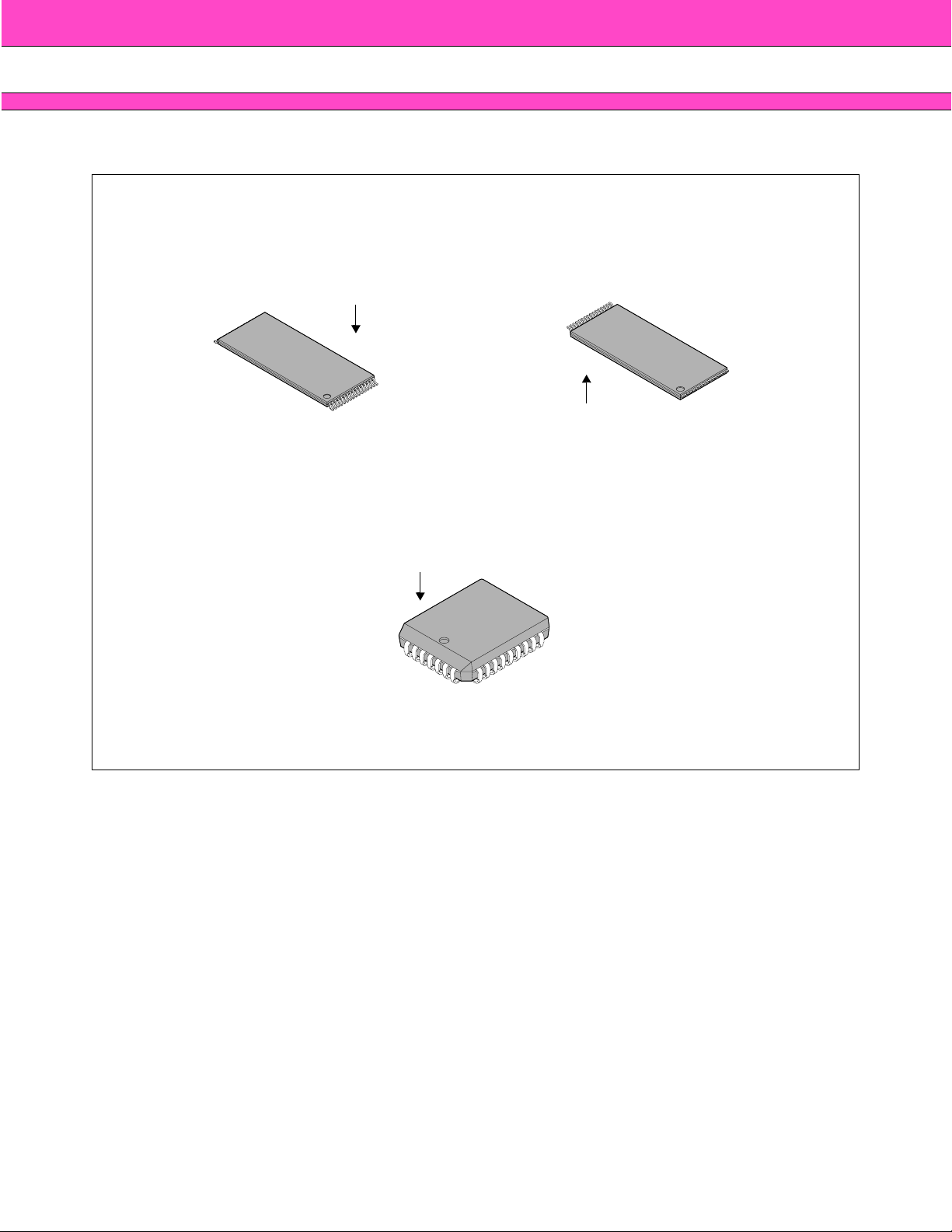
32-pin plastic TSOP(I)
Marking Side
(FPT-32P-M24)
32-pin plastic TSOP(I)
Marking Side
(FPT-32P-M25)
32-pin plastic QFJ (PLCC)
Marking Side
(LCC-32P-M02)
2

MBM29F002TC
GENERAL DESCRIPTION
■
The MBM29F002TC/BC is a 2 M-bit, 5.0 V-Only Flash memory organized as 256K bytes of 8 bits each. The
MBM29F002TC/BC is offered in a 32-pin TSOP(I) and 32-pin PLCC packages. This device is designed to be
programmed in-system with the standard system 5.0 V V
erase operations. The device can also be reprogrammed in standard EPROM programmers.
The standard MBM29F002TC/BC offers access times between 55 ns and 90 ns allowing oper ation of high-speed
microprocessors without wait states. To eliminate bus contention the de vice has separate chip enable (CE
enable (WE), and output enable (OE) controls.
The MBM29F002TC/BC is command set compatible with JEDEC standard E
to the command register using standard microprocessor write timings. Register contents serve as input to an
internal state-machine which controls the erase and programming circuitry. Write cycles also internally latch
addresses and data needed for the programming and er ase operations. Reading data out of the de vice is similar
to reading from 12.0 V Flash or EPROM devices.
The MBM29F002TC/BC is programmed by executing the program command sequence. This will invoke the
Embedded Program Algorithm which is an internal algorithm that automatically times the program pulse widths
and verifies proper cell margin. Each sector can be programmed and verified in less than 0.5 seconds. Erase
is accomplished by executing the erase command sequence. This will invoke the Embedded Erase Algorithm
which is an internal algorithm that automatically preprograms the array if it is not already programmed before
ex ecuting the erase operation. During erase, the device automatically times the er ase pulse widths and v erifies
proper cell margin.
-55/-70/-90
/MBM29F002BC
supply. A 12.0 V VPP is not required for program or
CC
2
PROMs. Commands are written
-55/-70/-90
), write
This device also features a sector erase architecture. The sector erase mode allows for sectors of memory to
be erased and reprogrammed without affecting other sectors. A sector is typically erased and verified within 1
second (if already completely preprogrammed). The MBM29F002TC/BC is erased when shipped from the
factory .
The MBM29F002TC/BC device also f eatures hardware sector protection. This feature will disab le both program
and erase operations in any number of secotrs (0 through 6)
Fujitsu has implemented an Erase Suspend feature that enab les the user to put erase on hold f or any period of
time to read data from or program data to a non-busy sector. Thus, true background erase can be achieved.
The device f eatures single 5.0 V power supply operation for both read and program functions . Internally generated
and regulated voltages are provided for the program and erase operations. A low V
inhibits write operations during power transitions. The end of program or erase is detected by Data Polling of
DQ
, or by the Toggle Bit I feature on DQ6. Once the end of a program or erase cycle has been completed, the
7
device automatically resets to the read mode.
The MBM29F002TC/BC also has a hardware RESET
Program or Embedded Erase operations will be terminated. The internal state machine will then be reset into
the read mode. The RESET
during the Embedded Program or Embedded Erase operation, the de vice will be automatically reset to a read
mode. This will enable the system microprocessor to read the boot-up firmware from the Flash memory.
Fujitsu's Flash technology combines years of EPROM and E
of quality, reliability , and cost eff ectiv eness. The MBM29F002TC/BC memory electrically erases all bits within a
sector simultaneously via Fowler-Nordheim tunneling. The bytes are programmed one byte at a time using the
EPROM programming mechanism of hot electron injection.
pin may be tied to the system reset circuity. Therefore, if a system reset occurs
pin. When this pin is driven low , execution of an y Embedded
.
detector automatically
CC
2
PROM experience to produce the highest levels
3

MBM29F002TC
FLEXIBLE SECTOR-ERASE ARCHITECTURE
■
• One 16K byte, two 8K bytes, one 32K byte, and three 64K bytes
• Individual-sector, multiple-sector, or bulk-erase capability
• Individual or multiple-sector protection is user definable
-55/-70/-90
/MBM29F002BC
-55/-70/-90
3FFFFH
16K byte
3BFFFH
8K byte
39FFFH
8K byte
37FFFH
32K byte
2FFFFH
64K byte
1FFFFH
64K byte
0FFFFH
64K byte
00000H
MBM29F002TC Sector Architecture MBM29F002BC Sector Architecture
64K byte
64K byte
64K byte
32K byte
8K byte
8K byte
16K byte
3FFFFH
2FFFFH
1FFFFH
0FFFFH
07FFFH
05FFFH
03FFFH
00000H
4
MBM29F002TC
PRODUCT LINE UP
■
-55/-70/-90
/MBM29F002BC
-55/-70/-90
Part No. MBM29F002TC/BC
V
= 5.0 V ± 5% -55 — —
CC
Ordering Part No.
V
= 5.0 V ± 10% — -70 -90
CC
Max. Address Access Time (ns) 55 70 90
Max. CE
Access Time (ns) 55 70 90
Max. OE Access Time (ns) 30 30 35
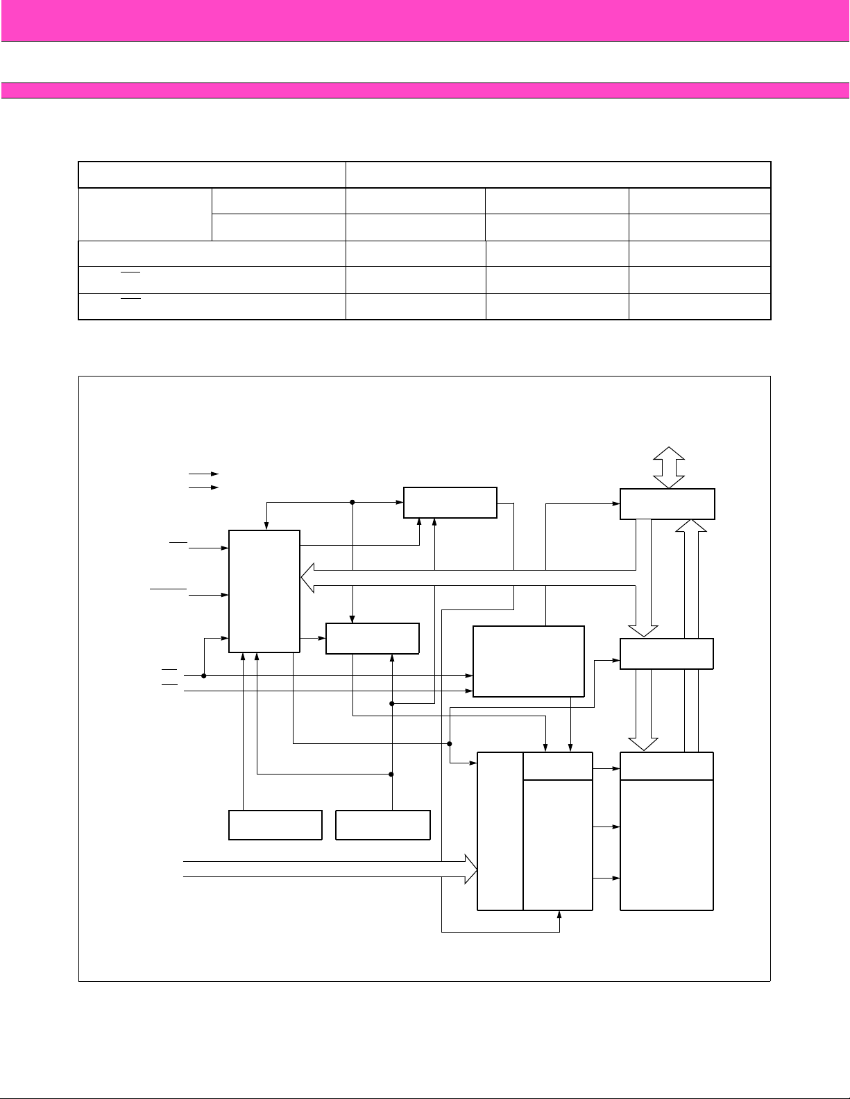
BLOCK DIAGRAM
■
DQ0 to DQ
CC
V
SS
V
WE
RESET
CE
OE
State
Control
Command
Register
Program Voltage
Generator
Erase Voltage
Generator
Chip Enable
Output Enable
Logic
STB
Input/Output
Buffers
Data Latch
7
A0 to A
STB
CC
Low V
Detector
17
Timer for
Program/Erase
Address
Latch
Y-Decoder
X-Decoder
Y-Gating
Cell Matrix
5
MBM29F002TC
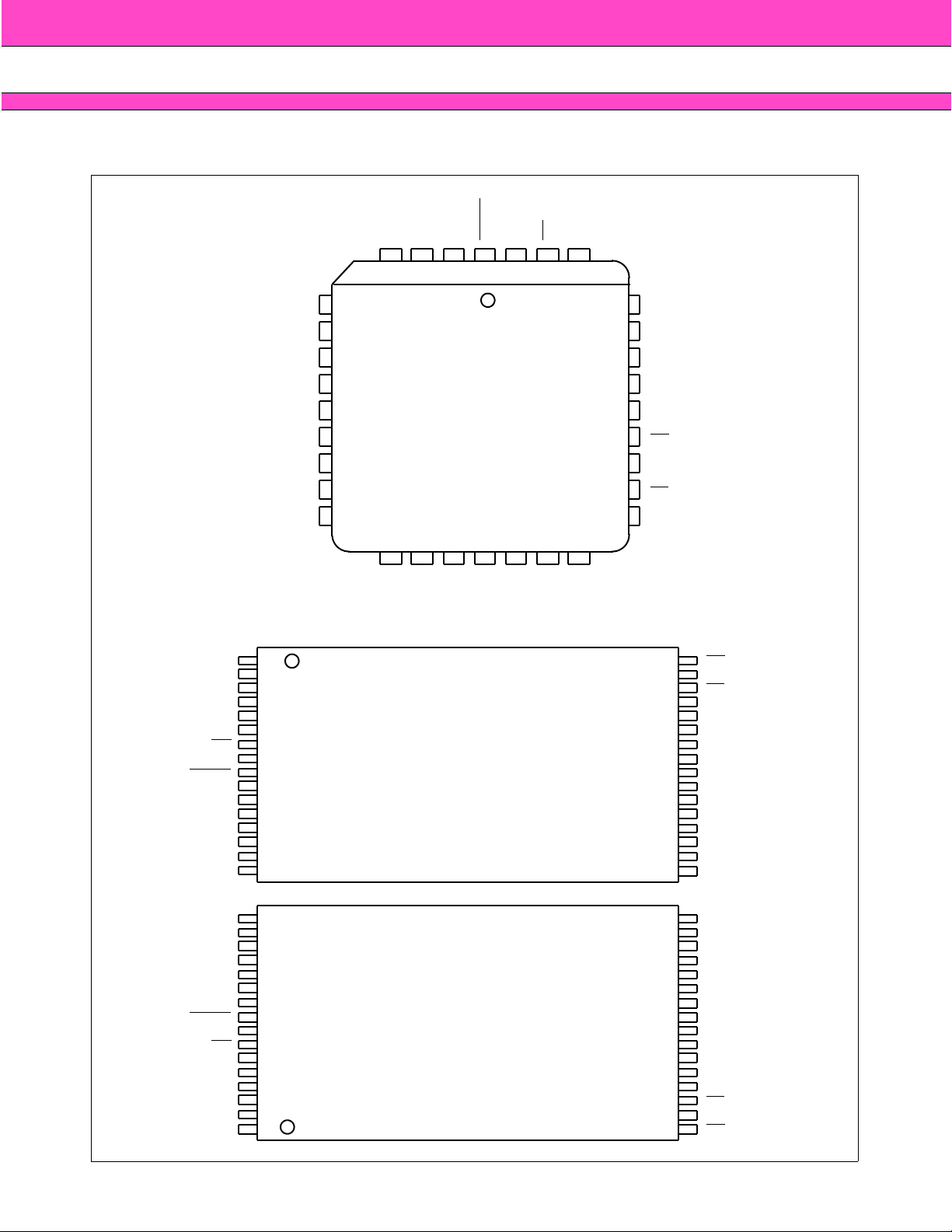
CONNECTION DIAGRAMS
■
-55/-70/-90
/MBM29F002BC
PLCC
-55/-70/-90
A
A
A
A
A
A
WE
V
RESET
A
A
A
A
A
A
A
12
15
A
16
A
A
CC
RESET
V
WE
17
A
4 3 2 1 32 31 30
A
A
A
A
A
A
A
A
DQ
7
5
6
6
5
7
4
8
3
9
2
10
1
11
0
12
0
13
29
28
27
26
25
24
23
22
21
A
A
A
A
A
OE
A
CE
DQ
14
13
8
9
11
10
7
14 15 16 17 18 19 20
1
DQ
2
DQ
SS
DQ3DQ 4DQ 5DQ
V
6
LCC-32P-M02
TSOP (I)
11
1
9
2
8
3
13
4
14
5
17
6
Marking Side
7
CC
8
9
10
16
11
15
12
12
13
7
14
6
15
5
16
4
Standard Pinout
32
31
30
29
28
27
26
25
24
23
22
21
20
19
18
17
OE
A
CE
DQ
DQ
DQ
DQ
DQ
V
DQ
DQ
DQ
A
A
A
A
10
7
6
5
4
3
SS
2
1
0
0
1
2
3
FPT-32P-M24
A
A
A
A
A
A
A
RESET
V
WE
A
A
A
A
A
A
4
15
5
14
6
13
7
12
12
11
15
10
16
Marking Side
9
CC
8
7
6
17
5
14
4
13
3
8
2
9
1
11
Reverse Pinout
17
18
19
20
21
22
23
24
25
26
27
28
29
30
31
32
A
A
A
A
DQ
DQ
DQ
V
DQ
DQ
DQ
DQ
DQ
CE
A
OE
3
2
1
0
0
1
2
SS
3
4
5
6
7
10
16
FPT-32P-M25
6
MBM29F002TC
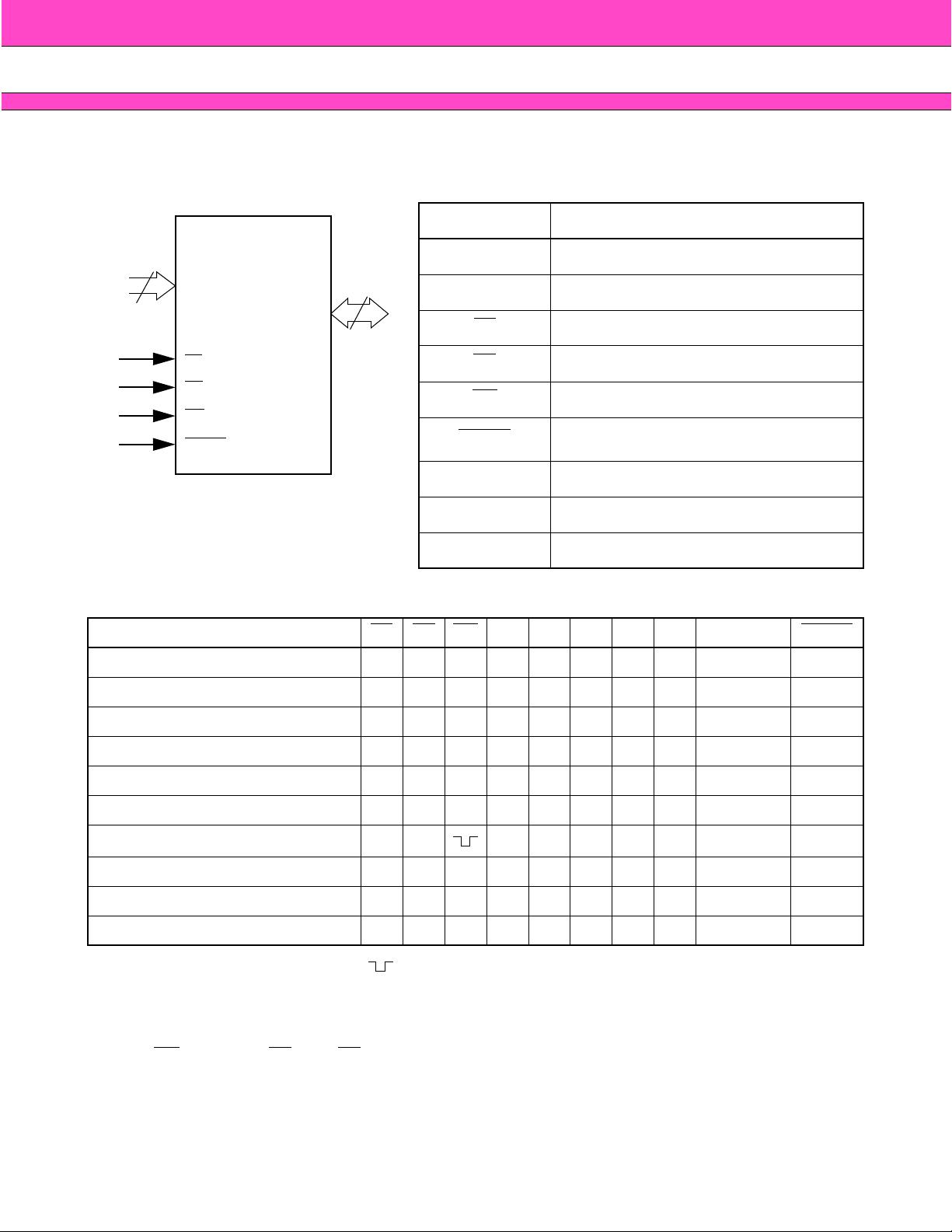
LOGIC SYMBOL
■
-55/-70/-90
Table 1 MBM29F002TC/BC Pin Configuration
Pin Function
/MBM29F002BC
-55/-70/-90
to A
A
0
to DQ
0
17
7
18
A 0 to A
17
DQ0 to DQ
8
7
DQ
CE
CE
OE
WE
RESET
OE
WE Write Enable
RESET
Hardware Reset Pin/Sector Protection
N.C. No Internal Connection
V
SS
V
CC
Table 2 MBM29F002TC/BC User Bus Operations
Operation CE
OE WE A
A1A6A9A10DQ0 to DQ7RESET
0
Auto-Select Manufacturer Code (1) L L H L L L V
Auto-Select Device Code (1) L L H H L L V
Address Inputs
Data Inputs/Outputs
Chip Enable
Output Enable
Unlock
Device Ground
Device Power Supply
LCode H
ID
LCode H
ID
Read (3) L L H A
0
A1A
6
A9A
10
D
OUT
H
Standby HXXXXXXX HIGH-Z H
Output Disable LHHXXXXX HIGH-Z H
Write (Program/Erase) L H L A
Enable Sector Protection (2) L V
ID
Verify Sector Protection (2) L L H L H L V
Temporary Sector Unprotection X X X X X X X X X V
0
A1A
6
A9A
10
D
IN
H
XXXVIDXX H
LCode H
ID
ID
Reset (Hardware) XXXXXXXX HIGH-Z L
Legend:
Notes:
L = VIL, H = VIH, X = VIL or VIH, = Pulse Input. See DC Characteristics for voltage levels.
1.Manufacturer and device codes ma y also be accessed via a command register write sequence. Refer to
Table 6.
2.Refer to the section on Sector Protection.
3.WE
can be VIL if OE is VIL, OE at VIH initiates the write operations.
7

MBM29F002TC
ORDERING INFORMATION
■
-55/-70/-90
/MBM29F002BC
-55/-70/-90
Standard Products
Fujitsu standard products are available in several packages. The order number is formed by a combination of:
MBM29F002 T C -70 PFTN
PACKAGE TYPE
PFTN = 32-Pin Thin Small Outline Package
(TSOP) Standard Pinout
PFTR = 32-Pin Thin Small Outline Package
(TSOP) Reverse Pinout
PD = 32-Pin Rectangular Plastic Leaded
Chip Carrier (PLCC)
SPEED OPTION
See Product Selector Guide
C = Device Revision
BOOT CODE SECTOR ARCHITECTURE
T = Top sector
B = Bottom sector
DEVICE NUMBER/DESCRIPTION
MBM29F002
2 Mega-bit (256K × 8-Bit) CMOS Flash Memory
5.0 V-only Read, Write, and Erase
8

MBM29F002TC
FUNCTIONAL DESCRIPTION
■
-55/-70/-90
/MBM29F002BC
-55/-70/-90
Read Mode
The MBM29F002TC/BC has two control functions which must be satisfied in order to obtain data at the outputs.
is the power control and should be used for a de vice selection. OE is the output control and should be used
CE
to gate data to the output pins if a device is selected.
Address access time (t
access time (t
) is the delay from stable addresses and stable CE to valid data at the output pins. The output
CE
enable access time is the delay from the falling edge of OE
addresses have been stable for at least t
) is equal to the delay from stable addresses to valid output data. The chip enable
ACC
to valid data at the output pins (assuming the
time).
ACC-tOE
Standby Mode
There are two ways to implement the standb y mode on the MBM29F002TC/BC de vices, one using both the CE
and RESET
When using both pins, a CMOS standby mode is achie ved with CE
pins; the other via the RESET pin only.
and RESET inputs both held at V
CC
Under this condition the current consumed is less than 5 µA. A TTL standby mode is achieved with CE
RESET
Algorithm operation, V
access time (t
When using the RESET
pins held at VIH. Under this condition the current is reduced to approximately 1 mA. During Embedded
Active current (I
CC
) from either of these standby modes.
CE
pin only, a CMOS standby mode is achieved with RESET input held at V
) is required even CE = VIH. The device can be read with standard
CC2
±0.3 V (CE
SS
= “H” or “L”). Under this condition the current consumed is less than 5 µA. A TTL standby mode is achiev ed with
RESET
1 mA. Once the RESET
pin held at VIL (CE = “H” or “L”). Under this condition the current required is reduced to approximately
pin is taken high, the device requires 500 ns of wake up time before outputs are valid
for read access.
In the standby mode the outputs are in the high impedance state, independent of the OE
input.
Output Disable
With the OE input at a logic high level (VIH), output from the device is disabled. This will cause the output pins
to be in a high impedance state.
±0.3 V.
and
Autoselect
The autoselect mode allows the reading out of a binary code from the device and will identify its manuf acturer
and type. This mode is intended for use b y prog r amming equipment for the purpose of automatically matching
the device to be programmed with its corresponding programming algorithm. This mode is functional over the
entire temperature range of the device.
To activate this mode, the programming equipment must force V
identifier bytes may then be sequenced from the device outputs by toggling address A
addresses are don't cares except A
, A1, A6 and A10. (See Table 3.)
0
The manufacturer and device codes may also be read via the command register, for instances when the
MBM29F002TC/BC is erased or programmed in a system without access to high voltage on the A
command sequence is illustrated in Table 6. (Refer to Autoselect Command section.)
Byte 0 (A
= VIL) represents the manufacturer's code (Fujitsu = 04H) and b yte 1 (A0 = VIH) represents the device
0
identifier code for MBM29F002TC = B0H, MBM29F002BC = 34H. These two b ytes are giv en in the table 3. All
identifiers for manuf actures and device will exhibit odd parity with DQ
the proper device codes when executing the Autoselect, A
1
The Autoselect mode also f acilitates the determination of sector protection in the system. By performing a read
operation at the address location XX02H with the higher order address bits A
desired sector address, the device will return 01H for a protected sector and 00H for a non-protected sector.
(11.5 V to 12.5 V) on address pin A9. Two
ID
from VIL to VIH. All
0
defined as the parity bit. In order to read
7
must be VIL. (See Table 3.)
, A14, A15, A16 and A17 set to the
13
pin. The
9
9
MBM29F002TC
Table 3 .1 MBM29F002TC/BC Sector Protection Verify Autoselect Codes
-55/-70/-90
/MBM29F002BC
-55/-70/-90
Type A
to A
13
17
Manufacture’s Code X V
MBM29F002TC X V
A
10
IL
IL
A
6
V
IL
V
IL
A
1
V
IL
V
IL
A
0
V
IL
V
IH
Code (HEX)
04H
B0H
Device Code
MBM29F002BC X V
Sector Protection
Sector
Addresses
IL
V
IL
V
IL
V
IL
V
IL
V
IH
V
IH
V
IL
34H
01H*
* :Outputs 01H at protected sector addresses and outputs 00H at unprotected sector addresses.
Table 3 .2 Expanded Autoselect Code Table
Type Code DQ
DQ
7
DQ
6
DQ
5
DQ
4
DQ
3
DQ
2
DQ
1
0
Manufacture’s Code 04H 00000100
MBM29F002TCB0H 10110000
Device Code
MBM29F002BC34H 00110100
Sector Protection 01H 00000001
Table 4 Sector Address Tables (MBM29F002TC)
A
17
A
16
A
15
A
14
A
13
Address Range
SA0 0 0 X X X 00000H to 0FFFFH
SA1 0 1 X X X 10000H to 1FFFFH
SA2 1 0 X X X 20000H to 2FFFFH
SA3 1 1 0 X X 30000H to 37FFFH
SA4 1 1 1 0 0 38000H to 39FFFH
SA5111013A000H to 3BFFFH
SA6 1 1 1 1 X 3C000H to 3FFFFH
Table 5 Sector Address Tables (MBM29F002BC)
A
17
A
16
A
15
A
14
A
13
Address Range
SA0 0 0 0 0 X 00000H to 03FFFH
SA1 0 0 0 1 0 04000H to 05FFFH
SA2 0 0 0 1 1 06000H to 07FFFH
SA3 0 0 1 X X 08000H to 0FFFFH
SA4 0 1 X X X 10000H to 1FFFFH
SA5 1 0 X X X 20000H to 2FFFFH
SA6 1 1 X X X 30000H to 3FFFFH
10

MBM29F002TC
-55/-70/-90
/MBM29F002BC
-55/-70/-90
Write
Device erasure and progr amming are accomplished via the command register. The contents of the register serve
as inputs to the internal state machine. The state machine outputs dictate the function of the device.
The command register itself does not occupy any addressab le memory location. The register is a latch used to
store the commands, along with the address and data information needed to execute the command. The
command register is written by bringing WE
the falling edge of WE or CE, whichever happens later; while data is latched on the rising edge of WE or CE,
whichever happens first. Standard microprocessor write timings are used.
Refer to AC Write Characteristics and the Erase/Programming Waveforms for specific timing parameters.
to VIL, while CE is at VIL and OE is at VIH. Addresses are latched on
Sector Protection
The MBM29F002TC/BC features hardware sector protection. This feature will disable both program and erase
operations in any number of sectors (0 through 6)
equipment at the user's site. The device is shipped with all sectors unprotected.
The sector protection feature is enabled using prog ramming
.
T o activ ate this mode, the programming equipment must f orce V
V
= 11.5 V), CE = VIL. The sector addresses (A13, A14, A15, A16, and A17) should be set to the sector to be
ID
protected. Tables 4 and 5 define the sector address for each of the seven (7) individual sectors. Programming
of the protection circuitry begins on the falling edge of the WE pulse and is terminated with the rising edge of
the same. Sector addresses must be held constant during the WE
protection waveforms and algorithm.
To verify programming of the protection circuitry, the programming equipment must force V
with CE
A
device will produce 00H for unprotected sector. In this mode, the lower order addresses, except for A
and A
codes.
It is also possible to determine if a sector is protected in the system by writing an Autoselect command. P erforming
a read operation at the address location XX02H, where the higher order addresses (A
are the desired sector address will produce a logical “1” at DQ
codes.
and OE at VIL and WE at VIH. Scanning the sector addresses (A13, A14, A15, A16, and A17) while (A10, A6,
, A0) = (0, 0, 1, 0) will produce a logical “1” code at device output DQ0 for a protected sector. Otherwise the
1
are DON’T CARES. Address locations with A1 = VIL are reserved for Autoselect man ufacturer and de vice
10
on address pin A9 and control pin OE, (suggest
ID
pulse. See figures 14 and 21 for sector
on address pin A9
ID
, A1, A6,
0
, A14, A15, A16, and A17)
13
for a protected sector . See Table 3 f or A utoselect
0
11

MBM29F002TC
-55/-70/-90
/MBM29F002BC
-55/-70/-90
Temporary Sector Unprotection
This feature allows temporary unprotection of previously protected sectors of the MBM29F002TC/BC device in
order to change data. The Sector Unprotection mode is activated by setting the RESET
V). During this mode, formerly protected sectors can be programmed or erased by selecting the sector addresses.
Once the 12 V is taken away from the RESET pin, all the previously protected sectors will be protected again.
Refer to Figures 14 and 21.
Table 6 MBM29F002TC/BC Command Definitions
pin to high voltage (12
Command
Sequence
Read/Reset* 1 XXXH F0H ——————————
Reset/Read* 3 555H AAH 2AA H 55H 555H F0H RA RD — — — —
Manufacture Code 3 555H AAH 2AAH 55H 555H 90H 00H 04H — — — —
Device Code 3 555H AAH 2AAH 55H 555H 90H 01H ID — — — —
Byte Pro g ram 4 555H AAH 2AAH 55H 555H A0H PA PD — — — —
Chip Erase 6 555H AAH 2 AAH 55H 555H 80H 555H AAH 2AAH 55H 555H 10H
Sector E rase 6 555H AAH 2AAH 55 H 555H 80H 555H AAH 2AAH 55H SA 30H
Sector Erase Suspend Erase can be suspended during sector erase with Addr (“H” or “L”), Data (B0H)
Sector Erase Resume Erase can be resumed after suspend with Addr (“H” or “L”), Data (30H)
Notes:
*: Either of the two reset commands will reset the device.
1.Address bits A
Sector Address (SA).
2.Bus operations are defined in Table 2.
3.RA = Address of the memory location to be read.
PA = Address of the memory location to be programmed. Addresses are latched on the falling edge of
the WE
SA = Address of the sector to be erased. The combination of A
any sector.
4.RD = Data read from location RA during read operation.
PD = Data to be programmed at location PA. Data is latched on the rising edge of WE
ID = Device Code (Refer to the section on Sector Protection Verify Autoselect Codes.)
Bus
Write
Cycles
Req'd
pulse.
First Bus
Write Cycle
Addr. Data Addr. Data Addr. Data Addr. Data Addr. Data Addr. Data
to A17 = X = “H” or “L” for all address commands except or Program Address (PA) and
11
Second Bus
Write Cycle
Third Bus
Write Cycle
Fourth Bus
Read/Write
Cycle
, A16, A15, A14, and A13 will uniquely select
17
Fifth Bus
Write Cycle
.
Sixth Bus
Write Cycle
Command Definitions
Device operations are selected by writing specific address and data sequences into the command register.
Writing incorrect address and data values or writing them in the improper sequence will reset the device to the
read mode. Table 6 defines the valid register command sequences. Note that the Erase Suspend (B0H) and
Erase Resume (30H) commands are valid only while the Sector Erase operation is in prog ress. Moreo v er , both
Read/Reset commands are functionally equivalent, resetting the device to the read mode.
12

MBM29F002TC
-55/-70/-90
/MBM29F002BC
-55/-70/-90
Read/Reset Command
The read or reset operation is initiated by writing the read/reset command sequence into the command register .
Microprocessor read cycles retrieve arra y data from the memory . The de vice remains enabled f or reads until the
command register contents are altered.
The device will automatically power-up in the read/reset state . In this case, a command sequence is not required
to read data. Standard microprocessor read cycles will retrieve array data. This default value ensures that no
spurious alteration of the memory content occurs during the power transition. Refer to the AC Read
Characteristics and Waveforms for the specific timing parameters.
Autoselect Command
Flash memories are intended for use in applications where the local CPU alters memory contents. As such,
manufacture and device codes must be accessible while the device resides in the target system. PROM
programmers typically access the signature codes by raising A
voltage onto the address lines is not generally desirable system design practice.
The device contains an autoselect command operation to supplement traditional PROM programming
methodology. The operation is initiated by writing the autoselect command sequence into the command register .
Following the command write, a read cycle from address XX00H retrie ves the manuf acture code of 04H. A read
cycle from address XX01H returns the device code D5H. (See Table 3).
to a high voltage. However, multiplexing high
9
All manufacturer and device codes will exhibit odd parity with the DQ
Sector state (protection or unprotection) will be informed by address XX02H.
Scanning the sector addresses (A
logical “1” at device output DQ
To terminate the operation, it is necessary to write the read/reset command sequence into the register and also
to write the Autoselect command during the operation, ex ecute it after writing Read/Reset command sequence.
, A16, A15, A14, and A13) while (A10, A6, A1, A0) = (0, 0, 1, 0) will produce a
17
for a protected sector.
0
defined as the parity bit.
7
Byte Programming
The device is programmed on a byte-by-byte basis. Programming is a four bus cycle operation. There are two
“unlock” write cycles. These are follo wed by the progr am set-up command and data write cycles. Addresses are
latched on the falling edge of CE
or WE, whichever happens first. The rising edge of CE or WE (whiche ver happens first) begins programming.
CE
Upon executing the Embedded Program Algorithm command sequence, the system is
further controls or timings. The device will automatically provide adequate internally generated program pulses
and verify the programmed cell margin.
This automatic programming operation is completed when the data on DQ
bit at which time the device returns to the read mode and addresses are no longer latched. (See T able 7, Hardware
Sequence Flags.) Therefore, the device requires that a valid address to the device be supplied by the system
at this particular instance of time. Data
programmed.
or WE, whichever happens later and the data is latched on the rising edge of
required to provide
not
is equivalent to data written to this
7
Polling must be performed at the memory location which is being
Any commands written to the chip during this period will be ignored. If a hardware reset occurs during the
programming operation, it is impossible to guarantee the data are being written.
Programming is allowed in any sequence and across sector boundaries. Beware that a data “0” cannot be
programmed back to a “1”. Attempting to do so ma y either hang up the device or result in an apparent success
according to the data polling algorithm but a read from reset/read mode will show that the data is still “0”. Only
erase operations can convert “0”s to “1”s.
TM
Figure 16 illustrates the Embedded Programming
Algorithm using typical command strings and bus operations.
13

MBM29F002TC
-55/-70/-90
/MBM29F002BC
-55/-70/-90
Chip Erase
Chip erase is a six bus cycle operation. There are two “unlock” write cycles. These are followed by writing the
“set-up” command. Two more “unlock” write cycles are then followed by the chip erase command.
Chip erase does
Algorithm command sequence the device will automatically program and v erify the entire memory for an all zero
data pattern prior to electrical erase. The system is not required to provide any controls or timings during these
operations.
The automatic erase begins on the rising edge of the last WE
when the data on DQ
mode.
Figure 17 illustrates the Embedded Erase™ Algorithm using typical command strings and bus operations.
require the user to program the device prior to erase . Upon ex ecuting the Embedded Erase
not
pulse in the command sequence and terminates
is “1” (see Write Operation Status section) at which time the device returns to read the
7
Sector Erase
Sector erase is a six bus cycle operation. There are two “unloc k” write cycles. These are f ollow ed by writing the
“set-up” command. Two more “unlock” write cycles are then follo wed by the Sector Er ase command. The sector
address (any address location within the desired sector) is latched on the falling edge of WE
(Data = 30H) is latched on the rising edge of WE. After time-out of 50
erase command, the sector erase operation will begin.
Multiple sectors may be erased concurrently b y writing the six bus cycle oper ations on Table 6. This sequence
is followed with writes of the Sector Erase command to addresses in other sectors desired to be concurrently
erased. The time between writes must be less than 50 µs otherwise that command will not be accepted and
erasure will start. It is recommended that processor interrupts be disabled during this time to guarantee this
condition. The interrupts can be re-enabled after the last Sector Erase command is written. A time-out of 50 µs
from the rising edge of the last WE
edge of the WE occurs within the 50
sector erase timer window is still open, see section DQ
Erase or Erase Suspend during this time-out period will reset the device to the read mode, ignoring the previous
command string. Resetting the device once ex ecution has begun will corrupt the data in that sector . In that case,
restart the erase on those sectors and allow them to complete. (Refer to the Write Operation Status section f or
DQ
, Sector Erase Timer operation.) Loading the sector erase buffer may be done in any sequence and with
3
any number of sectors (0 to 6).
will initiate the ex ecution of the Sector Erase command(s). If another falling
s time-out window the timer is reset. (Monitor DQ3 to determine if the
µ
, Sector Erase Timer .) Any command other than Sector
3
s from the rising edge of the last sector
µ
, while the command
Sector erase does
all memory locations in the sector(s) to be erased prior to electrical erase. When erasing a sector or sectors the
remaining unselected sectors are not affected. The system is
during these operations.
The automatic sector erase begins after the 50 µs time out from the rising edge of the WE
sector erase command pulse and terminates when the data on DQ
at which time the device returns to the read mode. Data polling must be perf ormed at an address within any of
the sectors being erased.
Figure 17 illustrates the Embedded Erase™ Algorithm using typical command strings and bus operations.
14
require the user to program the device prior to erase . The device automatically progr ams
not
required to provide any controls or timings
not
pulse for the last
is “1” (see Write Operation Status section)
7

MBM29F002TC
-55/-70/-90
/MBM29F002BC
-55/-70/-90
Erase Suspend
The Erase Suspend command allows the user to interrupt a Sector Erase operation and then perf orm data reads
from or programs to a sector not being erased. This command is applicable ONLY during a Sector Erase operation
which includes the time-out period for sector erase. The Erase Suspend command will be ignored if written
during the Chip Erase operation or Embedded Program Algorithm. Writing the Erase Suspend command during
the Sector Erase time-out results in immediate termination of the time-out period and suspension of the erase
operation.
Any other command written during the Erase Suspend mode will be ignored except the Erase Resume command.
Writing the Erase Resume command resumes the erase operation. The addresses are DON’T CARES when
writing the Erase Suspend or Erase Resume command.
When the Erase Suspend command is written during the Sector Erase operation, the device will take a maxim um
of 15 µs to suspend the erase operation. When the device has entered the er ase-suspended mode, the DQ
will be at logic “1”, and DQ
DQ
and DQ7 to determine if the erase operation has been suspended. Further writes of the Erase Suspend
6
command are ignored.
When the erase operation has been suspended, the device def aults to the erase-suspend-read mode . Reading
data in this mode is the same as reading from the standard read mode except that the data must be read from
sectors that have not been erase-suspended. Successiv ely reading from the erase-suspended sector while the
device is in the erase-suspend-read mode will cause DQ
will stop toggling. The user must use the address of the erasing sector for reading
6
to toggle. (See the section on DQ2.)
2
bit
7
After entering the erase-suspend-read mode, the user can program the device by writing the appropriate
command sequence for Byte Program. This program mode is known as the erase-suspend-program mode.
Again, programming in this mode is the same as programming in the regular Byte Program mode except that
the data must be programmed to sectors that are not erase-suspended. Successively reading from the erasesuspended sector while the device is in the erase-suspend-progr am mode will cause DQ
the erase-suspended program operation is detected by Data polling of DQ
is the same as the regular Byte Program operation. Note that DQ
while DQ
To resume the operation of Sector Erase, the Resume command (30H) should be written. Any further writes of
the Resume command at this point will be ignored. Another Erase Suspend command can be written after the
chip has resumed erasing.
can be read from any address.
6
must be read from the Byte Program address
7
, or by the Toggle Bit I (DQ6) which
7
to toggle. The end of
2
15

MBM29F002TC
Write Operation Status
-55/-70/-90
/MBM29F002BC
Table 7 Hardware Sequence Flags
-55/-70/-90
In Progress
Exceeded
Time Limits
Notes:
1.Performing successive read operations from the erase-suspended sector will cause DQ
2.Performing successive read operations from any address will cause DQ
3.Reading the byte address being programmed while in the erase-suspend program mode will indicate logic
Status DQ
Embedded Program Algorithm DQ
DQ
7
Toggle 0 0 1
7
DQ
6
DQ
5
Embedded Erase Algorithm 0 Toggle 0 1 Toggle
Erase Suspend Read
(Erase Suspended Sector)
Erase
Suspended
Mode
Erase Suspend Read
(Non-Erase Suspended Sector)
Erase Suspend Program
(Non-Erase Suspended Sector)
Embedded Program Algorithm DQ
1100
Data Data Data Data Data
DQ
Toggle
7
(Note 2)
Toggle 1 0 1
7
00
Embedded Erase Algorithm 0 Toggle 1 1 N/A
Erase
Suspended
Mode
“1” at the DQ
bit. However, successive reads from the erase-suspended sector will cause DQ2 to toggle.
2
Erase Suspend Program
(Non-Erase Suspended Sector)
DQ
Toggle 1 0 N/A
7
to toggle.
2
to toggle.
6
3
DQ
2
Toggle
(Note 1)
1
(Note 3)
DQ
7
Data Polling
The MBM29F002TC/BC device features Data
Polling as a method to indicate to the host that the embedded
algorithms are in progress or completed. During the Embedded Program Algorithm, an attempt to read the device
will produce the complement of the data last written to DQ
Algorithm, an attempt to read the device will produce the true data last written to DQ
Erase™ Algorithm, an attempt to read the device will produce a “0” at the DQ
Embedded Erase Algorithm an attempt to read the device will produce a “1” at the DQ
for Data Polling (DQ
Data
polling will also flag the entry into Erase Suspend. DQ7 will switch “0” to “1” at the start of the Erase Suspend
) is shown in Figure 18.
7
mode. Please note that the address of an erasing sector must be applied in order to observe DQ
. Upon completion of the Embedded Program
7
. During the Embedded
7
output. Upon completion of the
7
output. The flowchart
7
in the Erase
7
Suspend Mode.
During Program in Erase Suspend, Data
polling will perform the same as in regular program execution outside
of the suspend mode.
For chip erase, the Data
For sector erase, the Data
Polling is v alid after the rising edge of the sixth WE pulse in the six write pulse sequence.
Polling is valid after the last rising edge of the sector erase WE pulse. Data Polling
must be performed at sector address within any of the sectors being erased and not a sector that is within a
protected sector. Otherwise, the status may not be valid.
16

MBM29F002TC
-55/-70/-90
/MBM29F002BC
-55/-70/-90
Just prior to the completion of Embedded Algorithm operation DQ7 may change asynchronously while the output
enable (OE
) is asserted low. This means that the device is driving status information on DQ7 at one instant of
time and then that byte's valid data at the ne xt instant of time. Depending on when the system samples the DQ
output, it may read the status or valid data. Ev en if the device has completed the Embedded Algorithm operations
and DQ
has a valid data, the data outputs on DQ0 to DQ6 may be still inv alid. The v alid data on DQ0 to DQ7 will
7
be read on the successive read attempts.
7
The Data
Polling feature is only active during the Embedded Programming Algorithm, Embedded Erase
Algorithm, Erase Suspend, erase-suspend-program mode, or sector erase time-out. (See Table 7.)
See Figure 9 for the Data
DQ
6
Polling timing specifications and diagrams.
Toggle Bit I
The MBM29F002TC/BC also features the “Toggle Bit I” as a method to indicate to the host system that the
embedded algorithms are in progress or completed.
During an Embedded Program or Erase Algorithm cycle, successive attempts to read (OE
the device
at any address
Erase Algorithm cycle is completed, DQ
will result in DQ6 toggling between one and zero. Once the Embedded Program or
will stop toggling and valid data will be read on
6
toggling) data from
the next
successive
attempts. During programming, the Toggle Bit I is valid after the rising edge of the fourth WE pulse in the four
write pulse sequence. For chip erase , and sector erase the Toggle Bit I is valid after the rising edge of the sixth
WE
pulse in the six write pulse sequence. For Sector Erase, the Toggle Bit I is valid after the last rising edge of
the sector erase WE pulse. The Toggle Bit I is active during the sector erase time out.
In programming, if the sector being written to is protected, the Toggle Bit I will toggle for about 2 µs and then
stop toggling without the data having changed. In erase, the de vice will erase all the selected sectors e xcept f or
the ones that are protected. If all selected sectors are protected, the chip will toggle the Toggle Bit I for about
100 µs and then drop back into read mode, having changed none of the data.
Either CE
cause DQ
or OE toggling will cause the DQ6 to toggle. In addition, an Erase Suspend/Resume command will
to toggle.
6
See Figure 10 for the Toggle Bit I timing specifications and diagrams.
DQ
5
Exceeded Timing Limits
DQ
will indicate if the program or erase time has exceeded the specified limits (internal pulse count). Under
5
these conditions DQ
cycle was not successfully completed. Data P olling DQ
this condition. The CE
will produce a “1”. This is a failure condition which indicates that the program or erase
5
, DQ6 is the only operating function of the device under
7
circuit will partially power down the device under these conditions (to approximately 2
mA). The OE and WE pins will control the output disable functions as described in Table 2.
The DQ
failure condition ma y also appear if a user tries to program a 1 to a location that is previously programmed
5
to 0. In this case the device locks out and never completes the Embedded Algorithm operation. Hence, the
system never reads a v alid data on DQ
limits, the DQ
bit will indicate a “1.” Please note that this is not a device f ailure condition since the device was
5
bit and DQ6 never stops toggling. Once the de vice has e xceeded timing
7
incorrectly used. If this occurs, reset the device.
17

MBM29F002TC
DQ
3
Sector Erase Timer
-55/-70/-90
/MBM29F002BC
-55/-70/-90
After the completion of the initial sector erase command sequence the sector erase time-out will begin. DQ
remain low until the time-out is complete. Data Polling and Toggle Bit I are valid after the initial sector erase
command sequence.
If Data
Polling or the Toggle Bit I indicates the device has been written with a valid erase command, DQ3 may
be used to determine if the sector erase timer window is still open. If DQ
is high (“1”) the internally controlled
3
erase cycle has begun; attempts to write subsequent commands (other than Erase Suspend) to the device will
be ignored until the erase operation is completed as indicated by Data Polling or Toggle Bit I. If DQ
is low (“0”),
3
the device will accept additional sector erase commands. To insure the command has been accepted, the system
software should check the status of DQ
prior to and following each subsequent sector erase command. If DQ3
3
were high on the second status check, the command may not have been accepted.
Refer to Table 7: Hardware Sequence Flags.
DQ
2
Toggle Bit II
This toggle bit II, along with DQ
, can be used to determine whether the device is in the Embedded Erase™
6
Algorithm or in Erase Suspend.
Successive reads from the erasing sector will cause DQ
to toggle during the Embedded Erase™ Algorithm. If
2
the device is in the erase-suspended-read mode, successiv e reads from the erase-suspended sector will cause
DQ
to toggle. When the device is in the erase-suspended-program mode, successive reads from the byte
2
address of the non-erase suspended sector will indicate a logic “1” at the DQ
bit.
2
will
3
Mode DQ
Program DQ
7
7
DQ
6
toggles 1
DQ
Erase 0 toggles toggles
Erase Suspend Read (1)
(Erase-Suspended Sector)
Erase Suspend Program DQ
Notes:
1.These status flags apply when outputs are read from a sector that has been erase-suspended.
1 1 toggles
(2) toggles 1 (2)
7
2.These status flags apply when outputs are read from the byte address of the non-erase suspended sector.
DQ
is different from DQ2 in that DQ6 toggles only when the standard program or Erase, or Erase Suspend
6
Program operation is in progress. The behavior of these two status bits, along with that of DQ
, is summarized
7
as follows:
For e xample, DQ
DQ
does not). See also Table 7 and Figure 15.
6
Furthermore, DQ
mode, DQ
2
and DQ6 can be used together to determine the erase-suspend-read mode (DQ2 toggles while
2
can also be used to determine which sector is being erased. When the device is in the erase
2
toggles if this bit is read from the erasing sector.
2
18

MBM29F002TC
RESET
Hardware Reset
-55/-70/-90
/MBM29F002BC
-55/-70/-90
The MBM29F002TC/BC device ma y be reset by driving the RESET
(V
) for at least 500 ns. An y operation in progress will be terminated and the internal state machine will be reset
IL
to the read mode 20 µs after the RESET
the data at that particular location will be indeterminate.
When the RESET
accessed. Also, note that all the data output pins are tri-stated for the duration of the RESET
RESET pin is taken high, the device requires t
The RESET pin may be tied to the system reset input. Theref ore, if a system reset occurs during the Embedded
Program or Erase Algorithm, the device will be automatically reset to read mode and this will enab le the system’s
microprocessor to read the boot-up firmware from the Flash memory.
pin is low and the internal reset is complete, the device goes to standb y mode and cannot be
pin is driven low . If a hardware reset occurs during a program operation,
of wake up time until outputs are valid for read access.
RH
pin to VIL. The RESET pin must be kept low
pulse. Once the
19

MBM29F002TC
-55/-70/-90
/MBM29F002BC
-55/-70/-90
Data Protection
The MBM29F002TC/BC is designed to offer protection against accidental erasure or programming caused by
spurious system level signals that ma y e xist during power transitions . During power up the de vice automatically
resets the internal state machine in the Read mode. Also, with its control register architecture, alter ation of the
memory contents only occurs after successful completions of specific multi-bus cycle command sequences.
The device also incorporates several features to prevent inadvertent write cycles resulting from V
and power-down transitions or system noise.
power-up
CC
Low VCC Write Inhibit
To avoid initiation of a write cycle during VCC power-up and power-do wn, a write cycle is locked out for VCC less
than 3.2 V (typically 3.7 V). If V
are disabled. Under this condition the device will reset to the read mode . Subsequent writes will be ignored until
the V
to prevent unintentional writes when V
level is g reater than V
CC
< V
CC
LKO
, the command register is disabled and all internal program/erase circuits
LKO
. It is the users responsibility to ensure that the control pins are logically correct
is above 3.2 V.
CC
Write Pulse “Glitch” Protection
Noise pulses of less than 5 ns (typical) on OE, CE, or WE will not initiate a write cycle.
Logical Inhibit
Writing is inhibited by holding any one of OE = VIL, CE = VIH or WE = VIH. To initiate a write cycle CE and WE
must be a logical zero while OE
is a logical one.
Power-Up Write Inhibit
Power-up of the device with WE = CE = VIL and OE = VIH will not accept commands on the rising edge of WE.
The internal state machine is automatically reset to the read mode on power-up.
20

MBM29F002TC
ABSOLUTE MAXIMUM RATINGS
■
Storage Temperature ........................................................................................ –55°C to +125°C
Ambient Temperature with Power Applied ........................................................–40°C to +85°C
Voltage with Respect to Ground All pins except A
V
(Note 1) ......................................................................................................–2.0 V to +7.0 V
CC
A
, OE, and RESET (Note 2)............................................................................–2.0 V to +13.5 V
9
-55/-70/-90
/MBM29F002BC
, OE, and RESET (Note 1).–2.0 V to +7.0 V
9
-55/-70/-90
Notes:
WARNING:
■
WARNING:
1.Minimum DC voltage on input or I/O pins is –0.5 V. During voltage transitions, inputs may negative
overshoot V
+0.5 V. During voltage transitions, outputs may positive overshoot to V
2.Minimum DC input voltage on A
and RESET
voltage on A
difference between input voltage and power supply. (V
Semiconductor devices can be permanently damaged by application of stress (voltage, current,
temperature, etc.) in excess of absolute maximum ratings. Do not exceed these ratings.
to –2.0 V for periods of up to 20 ns. Maximum DC voltage on output and I/O pins is VCC
SS
+2.0 V for periods up to 20 ns.
CC
, OE, and RESET pins are –0.5 V. During voltage transitions, A9, OE,
9
pins may negative overshoot VSS to –2.0 V for periods of up to 20 ns. Maximum DC input
, OE, and RESET are +13.0 V which may ov ershoot to 14.0 V for periods up to 20 ns. V oltage
9
– VCC) do not exceed 9 V.
IN
RECOMMENDED OPERATING RANGES
Ambient Temperature (TA)................................................................................ –40°C to +85°C
V
Supply Voltages
CC
MBM29F002TC/BC-55 ................................................................................. +4.75 V to +5.25 V
MBM29F002TC/BC-70/-90........................................................................... +4.50 V to +5.50 V
Operating ranges define those limits between which the functionality of the device is guaranteed.
The recommended operating conditions are required in order to ensure the normal operation of the
semiconductor device. All of the device’s electrical characteristics are warranted when the device is
operated within these ranges.
Always use semiconductor devices within their recommended operating condition ranges. Operation
outside these ranges may adversely affect reliability and could result in device failure.
No warranty is made with respect to uses, operating conditions, or combinations not represented on
the data sheet. Users considering application outside the listed conditions are advised to contact their
FUJITSU representatives beforehand.
21

MBM29F002TC
MAXIMUM OVERSHOOT
■
-55/-70/-90
/MBM29F002BC
-55/-70/-90
V
V
+0.8 V
–0.5 V
–2.0 V
CC
+2.0 V
CC
+0.5 V
+2.0 V
20 ns
20 ns
20 ns
Figure 1 Maximum Negative Overshoot Waveform
20 ns
20 ns
20 ns
22
Figure 2 Maximum Positive Overshoot Waveform 1
+14.0 V
+13.0 V
CC
V
+0.5 V
Note: This waveform is applied for A9, OE, and RESET.
20 ns
Figure 3 Maximum Positive Overshoot Waveform 2
20 ns
20 ns
MBM29F002TC
DC CHARACTERISTICS
■
-55/-70/-90
/MBM29F002BC
-55/-70/-90
Parameter
Symbol
I
LI
I
LO
I
LIT
I
CC1
I
CC2
I
CC3
I
CC4
V
IL
V
IH
Parameter Description Test Conditions Min. Max. Unit
Input Leakage Current VIN = VSS to VCC, VCC = VCC Max. — ±1.0
= VSS to VCC,
V
Output Leakage Current
A9, OE, RESET Inputs Leakage
Current
OUT
V
= VCC Max.
CC
VCC = VCC Max.
A
, OE, RESET = 12.5 V
9
VCC Active Current (Note 1) CE = VIL, OE = V
VCC Active Current (Note 2) CE = VIL, OE = V
V
= VCC Max., CE = VIH
CC
RESET = V
IH
IH
IH
—±1.0µA
—50µA
—35mA
—50mA
—1mA
µ
VCC Current (Standby)
= VCC Max., CE = VCC ±0.3 V,
V
CC
RESET = V
V
= VCC Max.
CC
RESET = V
±0.3 V
CC
IL
—5µA
—1mA
VCC Current (Standby, Reset)
= VCC Max.
V
CC
RESET = V
±0.3 V
SS
—5µA
Input Low Level — –0.5 0.8 V
Input High Level — 2.0 VCC+0.5 V
A
V
ID
V
OL
V
OH1
V
OH2
V
LKO
Notes:
V oltage fo r Autoselect and Sector
Protection (A
, OE, RESET)
9
—11.512.5V
(Note 3, 4)
Output Low Voltage Level IOL = 12.0 mA, VCC = VCC Min. — 0.45 V
= –2.5 mA, VCC = VCC Min. 2.4 — V
I
OH
Output High Voltage Level
IOH = –100 µAV
–0.4 — V
CC
Low VCC Lock-Out Voltage — 3.2 4.2 V
1.The I
(at 6 MHz). The frequency component typically is 2 mA/MHz, with OE
2.I
current listed includes both the DC operating current and the frequency dependent component
CC
at VIH.
active while Embedded Algorithm (program or erase) is in progress.
CC
3.Applicable to sector protection function.
4.(V
– VCC) do not exceed 9 V.
ID
23

MBM29F002TC
AC CHARACTERISTICS
■
-55/-70/-90
• Read Only Operations Characteristics
/MBM29F002BC
-55/-70/-90
Parameter
Symbols
JEDEC Standard
t
AVAV
t
AVQV
t
ELQV
t
GLQV
t
EHQZ
t
GHQZ
t
AXQX
Note:
t
RC
t
ACC
t
CE
t
OE
t
DF
t
DF
t
OH
—t
READY
1.Test Conditions:
Read Cycle Time — Min. 55 70 90 ns
Address to Output Delay
Chip Enable to Output Delay OE = VILMax. 55 70 90 ns
Output Enable to Output Delay — Max. 30 30 35 ns
Chip Enable to Output HIGH-Z — Max. 20 20 20 ns
Output Enable to Output HIGH-Z — Max. 20 20 20 ns
Output Hold Time From Addresses,
CE
or OE, Whichever Occurs First
RESET Pin Low to Read Mode — Max. 20 20 20
Output Load: 1 TTL gate and 30 pF
Input rise and fall times: 5 ns
Input pulse levels: 0.0 V to 3.0 V
Timing measurement reference level
Input: 1.5 V
Output: 1.5 V
Description Test Setup
CE
= V
IL
OE = V
Max. 55 70 90 ns
IL
—Min.0 0 0ns
2. Test Conditions:
Note:
Output Load: 1 TTL gate and 100 pF
Input rise and fall times: 5 ns
Input pulse levels: 0.45 V to 2.4 V
Timing measurement reference level
-55
(Note1)
-70
(Note2)
Input: 0.8 V and 2.0 V
Output: 0.8 V and 2.0 V
-90
(Note2)
Unit
s
µ
Note:
Device
Under
Test
L
C
1. C
= 30 pF including jig capacitance
L
= 100 pF including jig capacitance
2. C
L
Figure 4 Test Conditions
IN3064
or Equivalent
6.2 k
Ω
5.0 V
2.7 k
Ω
Diodes = IN3064
or Equivalent
24

MBM29F002TC
• Write/Erase/Program Operations
-55/-70/-90
/MBM29F002BC
-55/-70/-90
Parameter Symbols
MBM29F002TC/BC
Description
JEDEC Standard -55 -70 -90
t
AVAV
t
AVWL
t
WLAX
t
DVWH
t
WHDX
—t
—t
t
GHWL
t
GHEL
t
ELWL
t
WLEL
t
WHEH
t
WC
t
AS
t
AH
t
DS
t
DH
OES
OEH
t
GHWL
t
GHEL
t
CS
t
WS
t
CH
Write Cycle Time Min. 55 70 90 ns
Address Setup Time Min. 0 0 0 ns
Address Hold Time Min. 40 45 45 ns
Data Setup Time Min. 25 30 45 ns
Data Hold Time Min. 0 0 0 ns
Output Enable Setup Time Min. 0 0 0 ns
Output Enable
Hold Time
Read Min. 0 0 0 ns
Toggle Bit I and Data Polling Min. 10 10 10 ns
Read Recover Time Before Write Min. 0 0 0 ns
Read Recover Time Before Write Min. 0 0 0 ns
CE Setup Time Min. 0 0 0 ns
WE Setup Time Min. 0 0 0 ns
CE Hold Time Min. 0 0 0 ns
Unit
t
EHWH
t
WLWH
t
ELEH
t
WHWL
t
EHEL
t
WHWH1
t
WHWH2
—t
—t
—t
—t
—t
—t
t
WH
t
WP
t
CP
t
WPH
t
CPH
t
WHWH1
t
WHWH2
VCS
VIDR
VLHT
WPP
OESP
CSP
WE Hold Time Min. 0 0 0 ns
Write Pulse Width Min. 30 35 45 ns
Write Pulse Width Min. 30 35 45 ns
Write Pulse Width High Min. 20 20 20 ns
Write Pulse Width High Min. 20 20 20 ns
Byte Programming Operation Typ. 8 8 8
µ
Typ. 1 1 1 sec
Sector Erase Operation (Note 1)
Max. 8 8 8 sec
VCC Setup Time Min. 50 50 50
Rise Time to V
ID
Min. 500 500 500 ns
Voltage Transition Time (Note 2) Min. 4 4 4
Write Pulse Width (Note 2) Min. 100 100 100
OE Setup Time to WE Active (Note 2) Min. 4 4 4
CE Setup Time to WE Active (Note 2) Min. 4 4 4
µ
µ
µ
µ
µ
(Continued)
s
s
s
s
s
s
25
MBM29F002TC
(Continued)
-55/-70/-90
/MBM29F002BC
-55/-70/-90
Parameter Symbols
JEDEC Standard -55 -70 -90
—t
—t
—t
Notes:
1.This does not include the preprogramming time.
2.This timing is for Sector Protection operation.
RP
RH
EOE
RESET Pulse Width Min. 500 500 500 ns
RESET Hold Time Before Read Min. 50 50 50 ns
Delay Time from Embedded Output Enable Max. 30 30 35 ns
Description
MBM29F002TC/BC
Unit
26
MBM29F002TC
SWITCHING WAVEFORMS
■
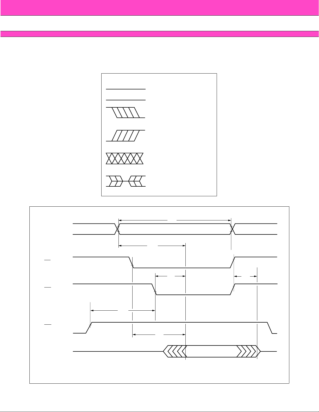
• Key to Switching Waveforms
-55/-70/-90
WAVEFORM INPUTS OUTPUTS
/MBM29F002BC
-55/-70/-90
Addresses
Must Be
Steady
May
Change
from H to L
May
Change
from L to H
“H” or “L”
Any Change
Permitted
Does Not
Apply
t RC
Addresses Stable
Will Be
Steady
Will Be
Changing
from H to L
Will Be
Changing
from L to H
Changing,
State
Unknown
Center Line is
HighImpedance
“Off” State
CE
OE
WE
DQ 0 to DQ 7
t ACC
t OE
t OEH
t CE
High-Z
Output Valid
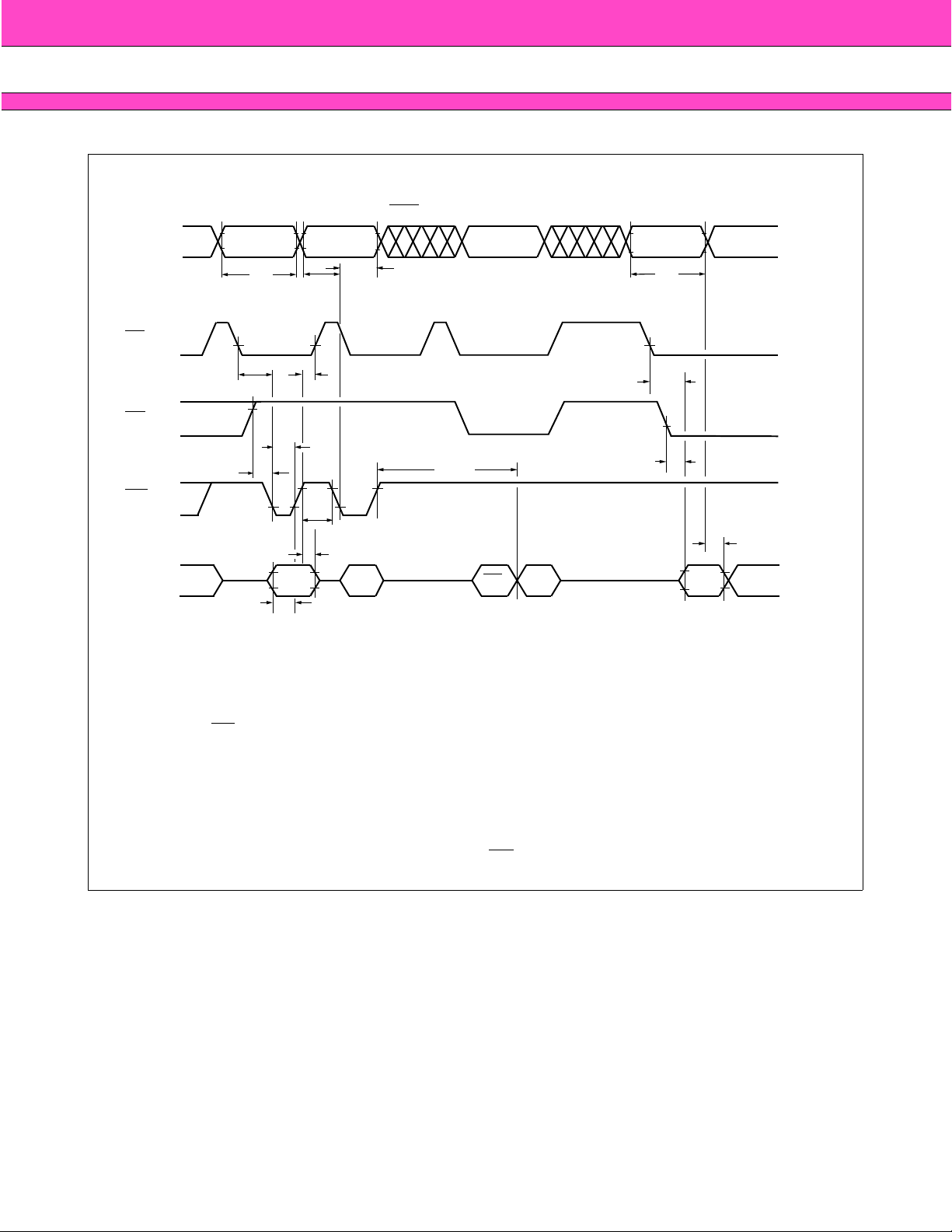
Figure 5.1 AC Waveforms for Read Operations
t DF
High-Z
27

MBM29F002TC
Addresses
RESET
-55/-70/-90
t RH
/MBM29F002BC
t RC
Addresses Stable
t ACC
-55/-70/-90
t OH
DQ 0 to DQ 7
High-Z
Output Valid
Figure 5.2 AC Waveforms for Read Operations
28
MBM29F002TC
Data Polling3rd Bus Cycle
-55/-70/-90
/MBM29F002BC
-55/-70/-90
Addresses
CE
OE
WE
Data
555H PA PA
AH
t
t
WPH
t
WP
t
AS
DH
t
PDA0H
GHWL
t
WC
t
CH
t
CS
t
DS
t
WHWH1
t
DQ
RC
t
CE
t
OE
t
OH
t
OUT
OUT
D
7
D
Notes:
1.PA is address of the memory location to be programmed.
2.PD is data to be programmed at byte address.
3.DQ
is the output of the complement of the data written to the device.
7
4.D
is the output of the data written to the device.
OUT
5.Figure indicates last two bus cycles of four bus cycle sequence.
Figure 6 AC Waveforms for Alternate WE Controlled Program Operations
29
MBM29F002TC
-55/-70/-90
/MBM29F002BC
Data Polling3rd Bus Cycle
-55/-70/-90
Addresses
WE
OE
CE
Data
555H PA PA
AH
t
CPH
t
AS
t
CP
DH
t
PDA0H
WHWH1
t
DQ
7
WC
t
t
WH
GHEL
t
WS
t
DS
t
t
D
OUT
Notes:
1.PA is address of the memory location to be programmed.
2.PD is data to be programmed at byte address.
3.DQ
is the output of the complement of the data written to the device.
7
4.D
is the output of the data written to the device.
OUT
5.Figure indicates last two bus cycles of four bus cycle sequence.
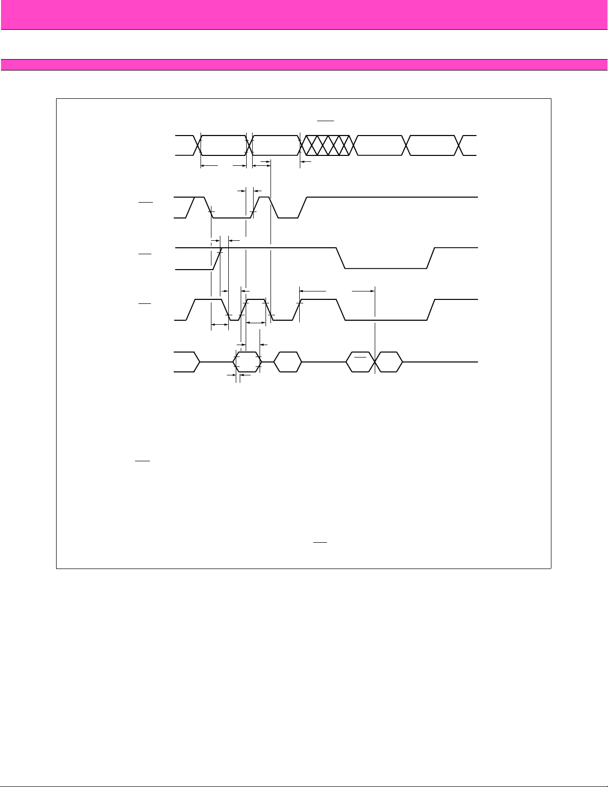
Figure 7 AC Waveforms for Alternate CE Controlled Program Operations
30
MBM29F002TC
-55/-70/-90
/MBM29F002BC
-55/-70/-90
Addresses
CE
OE
WE
Data
V CC
555H
t WC
t CS
t GHWL
t VCS
t WP
t DS
2AAH 555H
t AS t AH
t CH
t WPH
t DH
555H
2AAH SA*
55H55H 80H AAHAAH
10H/
30H
* : SA is the sector address for Sector Erase. Addresses = 555H for Chip Erase.
Figure 8 AC Waveforms Chip/Sector Erase Operations
31

MBM29F002TC
CH
CE
OE
t
-55/-70/-90
OEH
t
/MBM29F002BC
OE
t
-55/-70/-90
DF
t
WE
7
DQ
DQ0 to DQ
Data
6
Data
CE
t
WHWH1 or 2
t
*
7
DQ
EOE
t
DQ0 to DQ6 = Output Flug
DQ7 =
Valid Data
0
DQ
to DQ
Valid Data
7
* : DQ7 = Valid Data (The device has completed the Embedded operation.)
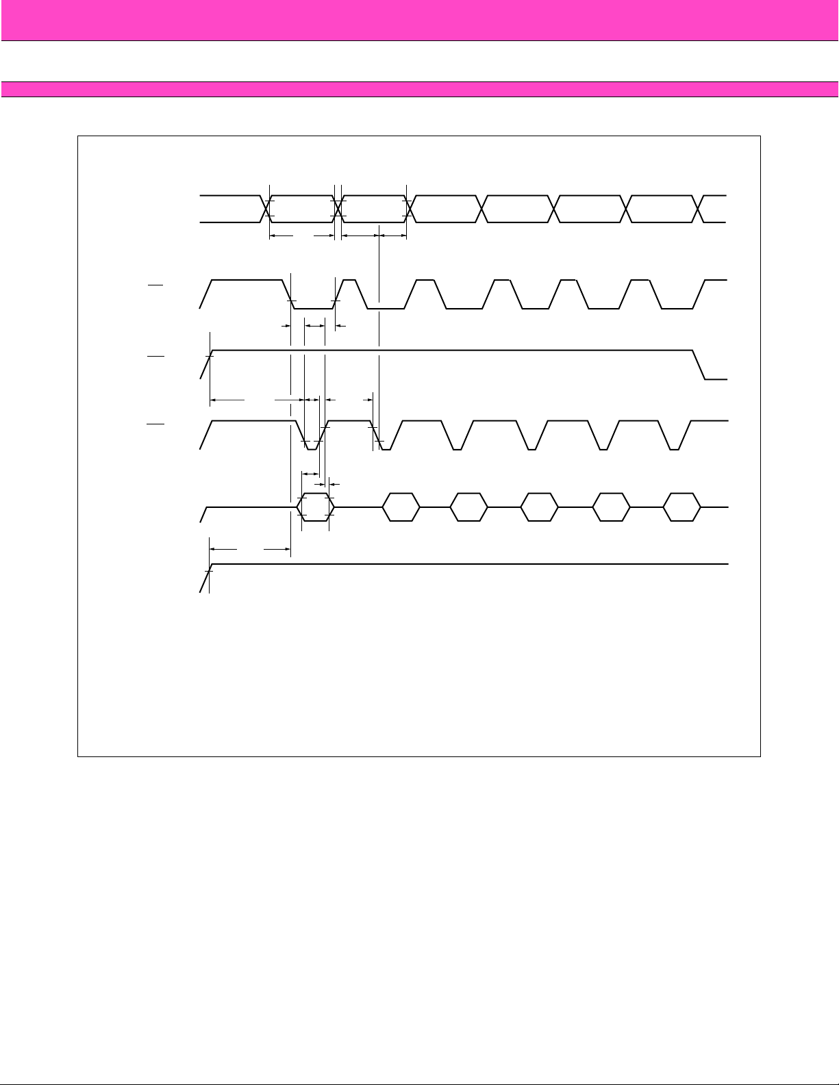
Figure 9 AC Waveforms for Data Polling During Embedded Algorithm Operations
CE
OEH
t
High-Z
High-Z
32
WE
OES
t
OE
*
DQ
6
Data
DQ6 = Toggle
DQ6 = Toggle
t
OE
DQ6 =
Stop Toggling
DQ
* : DQ6 stops toggling (The device has completed the Embedded operation.)
Figure 10 AC Waveforms for Toggle Bit I during Embedded Algorithm Operations
0
to DQ
Valid
7

MBM29F002TC
RESET
Figure 11 RESET Timing Diagram
-55/-70/-90
t
RP
t
READY
/MBM29F002BC
-55/-70/-90
33

MBM29F002TC
-55/-70/-90
/MBM29F002BC
-55/-70/-90
A17, A16, A15,
A
14, A13
A 0
A 1
A 6
V ID
5 V
A 9
ID
V
5 V
OE
WE
SAx SAy
t VLHT
t VLHT
t WPPt OESP
t VLHT
t VLHT
CE
Data
t VCS
V
CC
SGAx = Sector Address for initial sector
SGAy = Sector Address for next sector
t CSP
Figure 12 AC Waveforms for Sector Protection Timing Diagram
01H
t OE
34

CC
V
VID
5 V
RESET
CE
MBM29F002TC
tVIDR
tVCS
-55/-70/-90
/MBM29F002BC
tVLHT
-55/-70/-90
5 V
WE
DQ
WE
6
Enter
Embedded
Erasing
Program or Erase Command Sequence
tVLHT
Unprotection period
Figure 13 Temporary Sector Unprotection Timing Diagram
Erase
Erase
Suspend
Erase Suspend
Read
Enter Erase
Suspend Program
Erase
Suspend
Program
Erase
Resume
Erase Suspend
Read
tVLHT
Erase Erase
Complete
DQ
2
Note:
Toggle
2
DQ
and DQ6
with OE
DQ
is read from the erase-suspended sector.
2
Figure 14 DQ2 vs. DQ
6
35

MBM29F002TC
EMBEDDED ALGORITHMS
-55/-70/-90
/MBM29F002BC
Start
Write Program Command
Sequence
(See Below)
Polling Device
Data
-55/-70/-90
Increment Address Last Address
Program Command Sequence (Address/Command):
No
?
Yes
Programming Completed
555H/AAH
2AAH/55H
555H/A0H
Program Address/Program Data
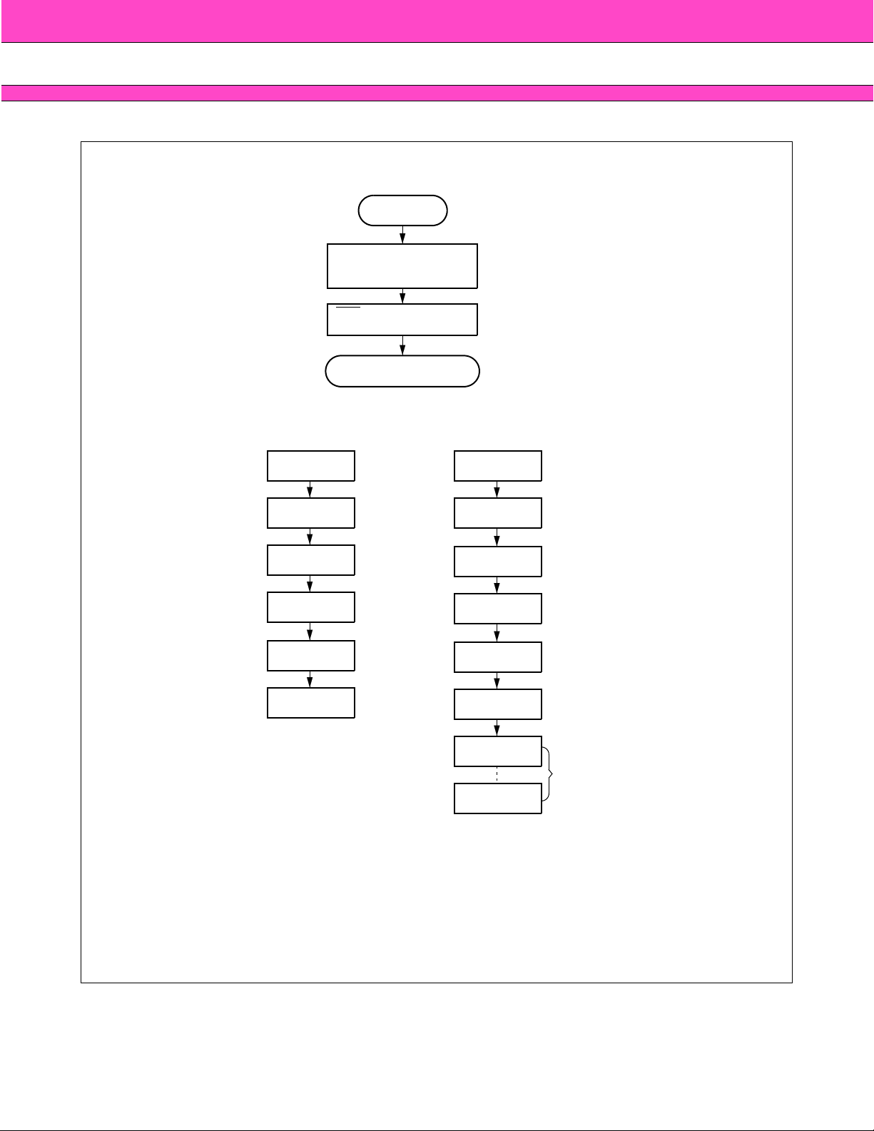
Figure 15 Embedded ProgramTM Algorithm
36
MBM29F002TC
Write Erase Command
Data
Polling or Toggle Bit I
Successfully Completed
Erasure Completed
-55/-70/-90
Start
Sequence
(See Below)
/MBM29F002BC
-55/-70/-90
Chip Erase Command Sequence
(Address/Command):
555H/AAH
2AAH/55H
555H/80H
555H/AAH
2AAH/55H
555H/10H
Individual Sector/Multiple Sector
Erase Command Sequence
(Address/Command):
555H/AAH
2AAH/55H
555H/80H
555H/AAH
2AAH/55H
Sector Address/30H
Sector Address/30H
Sector Address/30H
Additional sector
erase commands
are optional.
To insure the command has been accepted, the system software should check the status
Note:
of DQ
prior to and following each subsequent sector erase command. If DQ3 were high on
3
the second status check, the command may not have been accepted.
Figure 16 Embedded Erase™ Algorithm
37

MBM29F002TC
-55/-70/-90
Start
/MBM29F002BC
-55/-70/-90
Note:
Read Byte
0
(DQ
to DQ7)
Addr. = VA
VA = Address for programming
= Any of the sector addresses
within the sector being erased
during sector erase or multiple
erases operation.
DQ7 = Data?
Yes
= Any of the sector
addresses within the sector not
being protected during sector
erase or multiple sector erases
No
No
DQ5 = 1?
operation.
Yes
Read Byte
0
(DQ
to DQ7)
Addr. = VA
DQ7 = Data?
Fail
DQ
is rechecked even if DQ5 = “1” because DQ7 may change simultaneously with DQ5.
7
Yes
No
Pass
38
Figure 17 Data Polling Algorithm

MBM29F002TC
Addr. = “H” or “L”
-55/-70/-90
Start
Read Byte
0
(DQ
to DQ7)
/MBM29F002BC
-55/-70/-90
DQ
Note:
changing to “1”.
DQ6 = Toggle
?
No
is rechecked e ven if DQ5 = “1” because DQ6 may stop toggling at the same time as DQ5
6
DQ5 = 1
?
Read Byte
0
to DQ7)
(DQ
Addr. = “H” or “L”
DQ6 = Toggle
?
Fail
No
Yes
Yes
No
Yes
Pass
Figure 18 Toggle Bit I Algorithm
39

MBM29F002TC
-55/-70/-90
/MBM29F002BC
Start
-55/-70/-90
Increment PLSCNT
No
No
Setup Sector Addr.
(
A17, A16, A15, A14, A
PLSCNT = 1
OE
= VID, A9 = VID,
= VIL, RESET = V
CE
Activate WE Pulse
Time out 100 µs
IH,
WE = V
(A9 should remain VID)
CE = OE = V
Read from Sector
19
Addr. (A
A
, A18, A17)
1
= 1, A0 = A6 = 0
Data = 01H?PLSCNT = 25?
13
)
IH
IL,
40
Yes
Remove VID from A
Write Reset Command
Device Failed
Figure 19 Sector Protection Algorithm
Yes
9
Protect Another Sector?
No
Remove
Write Reset Command
VID from A
Sector Protection
Completed
Yes
9

MBM29F002TC
-55/-70/-90
Start
/MBM29F002BC
-55/-70/-90
Notes:
RESET = V
(Note 1)
Perform Erase or
Program Operations
RESET = V
Temporary Sector
Unprotection Completed
(Note 2)
1.All Protected sectors unprotected.
2.All previously protected sectors are protected once again.
Figure 20 Temporary Sector Unprotection Algorithm
ID
IH
41
MBM29F002TC
ERASE AND PROGRAMMING PERFORMANCE
■
-55/-70/-90
/MBM29F002BC
-55/-70/-90
Parameter
Sector Erase Time — 1 8 sec
Byte Programming Time — 8 150
Chip Programming Time — 2.1 5 sec
Erase/Program Cycle 100,000 — — cycles
TSOP(I) PIN CAPACITANCE
■
Parameter
Symbol
C
IN
C
OUT
C
IN2
Test conditions T
Note:
Parameter Description Test Setup Typ. Max. Unit
Input Capacitance VIN = 0 7 8 pF
Output Capacitance V
Control Pin Capacitance VIN = 0 8 10 pF
= 25°C, f = 1.0 MHz
A
Min. Typ. Max.
Limits
= 0 8 10 pF
OUT
Unit Comments
µ
Excludes 00H programming
prior to erasure
Excludes system-level
s
overhead
Excludes system-level
overhead
PLCC PIN CAPACITANCE
■
Parameter
Symbol
C
IN
C
OUT
C
IN2
Notes:
1. Sampled, not 100% tested.
2. Test conditions T
Parameter Description Test Setup Typ. Max. Unit
Input Capacitance VIN = 0 7 8 pF
Output Capacitance V
Control Pin Capacitance VIN = 0 8 10 pF
= 25°C, f = 1.0 MHz
A
= 0 8 10 pF
OUT
42
MBM29F002TC
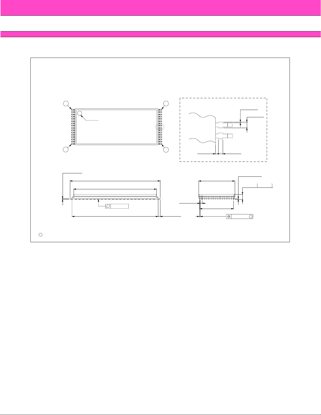
PACKAGE DIMENSIONS
■
32-pin plastic TSOP(I)
(FPT-32P-M24)
-55/-70/-90
/MBM29F002BC
-55/-70/-90
LEAD No.
C
1994 FUJITSU LIMITED F32035S-2C-1
1 32
INDEX
16
0.15±0.05
(.006±.002)
20.00±0.20
(.787±.008)
18.40±0.20
(.724±.008)
0.10(.004)
19.00±0.20
(.748±.008)
"A"
17
0.50±0.10
(.020±.004)
Details of "A" part
0.15(.006) 0.25(.010)
0.50(.0197)
TYP
8.00±0.20
(.315±.008)
7.50(.295)
REF.
0.20±0.10
(.008±.004)
0.15(.006)
MAX
0.35(.014)
MAX
0.05(.002)MIN
(STAND OFF)
+0.10
+.004
–0.05
1.10
0.10(.004)
(Mounting height)
M
.043
–.002
Dimensions in mm(inches)
43

MBM29F002TC
32-pin plastic TSOP(I)
(FPT-32P-M25)
-55/-70/-90
/MBM29F002BC
-55/-70/-90
LEAD No.
0.15±0.05
(.006±.002)
C
1997 FUJITSU LIMITED F32036S-2C-2
1
INDEX
16
19.00±0.20
(.748±.008)
0.10(.004)
18.40±0.20
(.724±.008)
20.00±0.20
(.787±.008)
"A"
32
17
0.50±0.10
(.020±.004)
Details of "A" part
0.50(.0197)
TYP
0.20±0.10
(.008±.004)
7.50(.295)
REF.
8.00±0.20
(.315±.008)
0.15(.006)
MAX
0.35(.014)
MAX
0.25(.010)0.15(.006)
0.10(.004)
M
0.05(.002)MIN
(STAND OFF)
+0.10
–0.05
1.10
(Mounting height)
.043
+.004
–.002
Dimensions in mm(inches)
44

MBM29F002TC
32-pin plastic QFJ(PLCC)
(LCC-32P-M02)
-55/-70/-90
/MBM29F002BC
-55/-70/-90
12.37±0.13
(.487±.005)
11.43±0.08
(.450±.003)
14 32 30
5
INDEX
13 21
2014
0.66(.026)
TYP
0.43(.017)
TYP
10.41±0.51
(.410±.020)
29
13.97±0.08
(.550±.003)
+0.05
–0.02
0.20
+.002
.008 –.001
0.10(.004)
14.94±0.13
(.588±.005)
3.40±0.16
(.134±.006)
2.25±0.38
(.089±.015)
0.64(.025)
MIN
12.95±0.51
(.510±.020)
R0.95(.037)
TYP
7.62(.300)REF
1.27±0.13
(.050±.005)
No
: LEAD No.
10.16(.400)
REF
C
1994 FUJITSU LIMITED C32021S-2C-4
Dimensions in mm(inches)
45

MBM29F002TC
-55/-70/-90
FUJITSU LIMITED
For further information please contact:
Japan
FUJITSU LIMITED
Corporate Global Business Support Division
Electronic Devices
KAWASAKI PLANT, 4-1-1, Kamikodanaka
Nakahara-ku, Kawasaki-shi
Kanagawa 211-8588, Japan
Tel: (044) 754-3763
Fax: (044) 754-3329
/MBM29F002BC
All Rights Reserved.
The contents of this document are subject to change without
notice. Customers are advised to consult with FUJITSU sales
representatives before ordering.
-55/-70/-90
http://www.fujitsu.co.jp/
North and South America
FUJITSU MICROELECTRONICS, INC.
Semiconductor Division
3545 North First Street
San Jose, CA 95134-1804, USA
Tel: (408) 922-9000
Fax: (408) 922-9179
Customer Response Center
Mon. - Fri.: 7 am - 5 pm (PST)
Tel: (800) 866-8608
Fax: (408) 922-9179
http://www.fujitsumicro.com/
Europe
FUJITSU MIKROELEKTRONIK GmbH
Am Siebenstein 6-10
D-63303 Dreieich-Buchschlag
Germany
Tel: (06103) 690-0
Fax: (06103) 690-122
http://www.fujitsu-ede.com/
Asia Pacific
FUJITSU MICROELECTRONICS ASIA PTE LTD
#05-08, 151 Lorong Chuan
New Tech Park
Singapore 556741
Tel: (65) 281-0770
Fax: (65) 281-0220
http://www.fmap.com.sg/
The information and circuit diagrams in this document are
presented as examples of semiconductor device applications,
and are not intended to be incorporated in devices for actual use.
Also, FUJITSU is unable to assume responsibility for
infringement of any patent rights or other rights of third parties
arising from the use of this information or circuit diagrams.
FUJITSU semiconductor devices are intended for use in
standard applications (computers, office automation and other
office equipment, industrial, communications, and measurement
equipment, personal or household devices, etc.).
CAUTION:
Customers considering the use of our products in special
applications where failure or abnormal operation may directly
affect human lives or cause physical injury or property damage,
or where extremely high levels of reliability are demanded (such
as aerospace systems, atomic energy controls, sea floor
repeaters, vehicle operating controls, medical devices for life
support, etc.) are requested to consult with FUJITSU sales
representatives before such use. The company will not be
responsible for damages arising from such use without prior
approval.
Any semiconductor devices have an inhereut chance of
failure. You must protect against injury, damage or loss from
such failures by incorporating safety design measures into your
facility and equipment such as redundancy, fire protection, and
prevention of over-current levels and other abnormal operating
conditions.
If any products described in this document represent goods or
technologies subject to certain restrictions on export under the
Foreign Exchange and Foreign Trade Law of Japan, the prior
authorization by Japanese government will be required for
export of those products from Japan.
46
F9903
FUJITSU LIMITED Printed in Japan
 Loading...