

Page 1

查询CS81 Series供应商
To Top / Lineup / Index
FUJITSU SEMICONDUCTOR
DATA SHEET
Semicustom
CMOS
Standard cell array
CS81 Series
DESCRIPTION
■
The CS81 series of 0.18 µm CMOS standard cell arrays is a line of highly integrated CMOS ASICs f eaturing high
speed and low power consumption at the same time.
DS06-20206-1E
This series incorporates up to 40 million gates which have a gate delay time of 11 ps, resulting in both integr ation
and speed about three times higher than conventional products.
In addition, this series can operate at a power-supply voltage of up to 1.1 V, substantially reducing power consumption.
FEATURES
■
• Technology : 0.18 µm silicon-gate CMOS, 3- to 5-layer wiring capable of integrating a mixture of highspeed processes and cells on a single chip (under development)
• Supply voltage : +1.8 V ± 0.15 V (typical) to +1.1 V ± 0.1 V
• Junction temperature range : −40 to +125 °C (standard specification)
• Gate delay time : t
• Gate power consumption : 5 nW/MHz/BC (1.1 V, 2-NAND, F/O = 1)
• High-load drive capability : I
• Output buffer cells with noise reduction circuits
• Inputs with on-chip input pull-up/pull-down resistors (33 kΩ typical) and bidirectional buffer cells
• Buffer cell dedicated to crystal oscillator
• Special interfaces (P-CML, LVDS, PCI, AGP, USB, SDRAM-I/F, SSTL, etc. under development)
• IP macros (CPU, DSP, PCI, IEEE1394, USB, IrDA, PLL, ADC, DAC, etc. under development)
• Capable of incorporating compiled cells (RAM/ROM/multiplier, etc.)
• Configurable internal bus circuits
• Advanced hardware/software co-design environment
• Short-term development using a timing driven layout tool
• Support for static timing sign-off
Dramatically reducing the time for generating test vectors for timing verification and the simulation time
• Hierarchical design environment for supporting large-scale circuits
• Simulation (before layout) considering the input slew rate and detailed RC delay calculation (after layout) ,
supporting development with minimized timing trouble after trial manufacture
• Support for memory (RAM/ROM) SCAN
• Support for memory (RAM) BIST
• Support for boundary SCAN
= 11 ps (1.8 V, inverter, F/O = 1)
pd
= 2/4/8/12 mA mixable
OL
(Continued)
Page 2
CS81 Series
(Continued)
• Support for path delay test
• A variety of package options (TQFP, HQFP, EBGA, FBGA, TAB-BGA, FCBGA)
MACRO LIBRARY (Including macros being prepared)
■
1. Logic cells (about 400 types)
• Adder • Decoder
• AND-OR Inverter • Non-SCAN Flip Flop
•Clock Buffer •Inverter
•Latch •Buffer
• NAND • OR-AND Inverter
•AND •OR
•NOR •Selector
• SCAN Flip Flop • BUS Driver
•ENOR •EOR
•AND-OR •Others
To Top / Lineup / Index
2. IP macros
CPU/DSP
Interface macro PCI, IEEE1394, USB, IrDA, etc.
Multimedia processing macros JPEG, MPEG, etc.
Mixed signal macros ADC, DAC, OPAMP, etc.
Compiled macros RAM, ROM, multiplier, adder, multiplier-accumulator, etc.
PLL Analog PLL, digital PLL
FR, SPARClite, standard CPU (under preparation)
Communications DSP, DSP for AV
3. Special I/O interface macros
• T-LVTTL • SSTL • HSTL • P-CML
• LVDS • PCI • AGP • USB
• IEEE1394
2
Page 3
To Top / Lineup / Index
CS81 Series
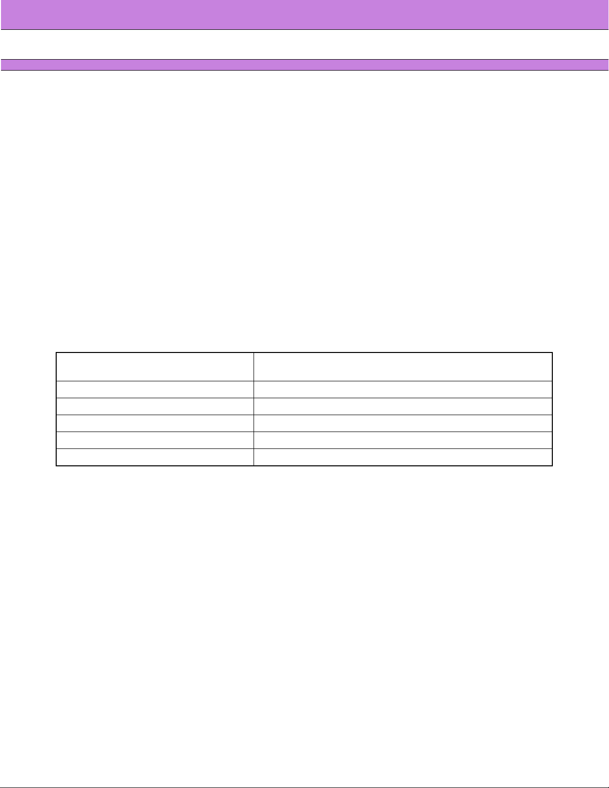
COMPILED CELLS
■
Compiled cells are macro cells which are automatically generated with the bit/word configuration specified. The
CS81 series has the following types of compiled cells. (Note that each macro is different in word/bit range
depending on the column type.)
1. Clock synchronous single-port RAM (1 address, 1 RW)
Column type Memory capacity Word range Bit range Unit
4 16 to 72 K 16 to 1 K 1 to 72 Bit
16 64 to 72 K 64 to 4 K 1 to 18 Bit
2. Clock synchronous dual-port RAM (2 addresses, 1 RW/ 1 R)
Column type Memory capacity Word range Bit range Unit
4 16 to 72 K 16 to 1 K 1 to 72 Bit
16 64 to 72 K 64 to 4 K 1 to 18 Bit
3. Clock synchronous ROM
Column type Memory capacity Word range Bit range Unit
8 128 to 512 K 32 to 4 K 4 to 128 Bit
16 128 to 512 K 64 to 8 K 2 to 64 Bit
HIGH-CAPACITY MEMORY
■
•
Clock synchronous single port RAM (1 address, 1 RW)
Column type Memory capacity Word range Bit range Unit
Under development
3
Page 4
CS81 Series
ABSOLUTE MAXIMUM RATINGS
■
Parameter Symbol Application
To Top / Lineup / Index
Rating
Min. Max.
(V
= 0 V)
SS
Unit
Power supply voltage V
Input voltage
*1
Output voltage V
Storage temperature T
Power-supply pin current
*2
VDD, V
DD
V
DDE
1.8 V input pin VSS − 0.5
V
I
3.3 V input pin V
1.8 V output pin VSS − 0.5
O
3.3 V output pin V
Plastic package −55 +125 °C
ST
Per VDD/V
I
D
Per V
(Internal) VSS − 0.5 +2.5 V
DDI
(External) VSS − 0.5 +4.0 V
+ 0.5
V
DDI
( ≤ 2.5 V)
+ 0.5
V
− 0.5
SS
DDE
( ≤ 4.0 V)
+ 0.5
V
DDI
( ≤ 2.5 V)
+ 0.5
V
− 0.5
SS
DDI/VDDE
pin TBD mA
SS
pin TBD mA
DDE
( ≤ 4.0 V)
L type output buffer IOL = 2 mA ±13 mA
Output current
*3
M type output buffer I
I
O
H type output buffer I
V type output buffer I
= 4 mA ±13 mA
OL
= 8 mA ±13 mA
OL
= 12 mA ±26 mA
OL
*1 : Do not apply any voltage of 1.1 V or more between the LVDS (resistor built-in type) differential inputs.
*2 : Maximum supply current which can be supplied constantly.
V
V
V
V
*3 : Maximum output current which can be supplied constantly . Exceeding the r ating is allowed only within 1 second
for only one LSI pin. The maximum rating of the P-CML output buffer is 20 mA.
WARNING: Semiconductor devices can be permanently damaged by application of stress (voltage, current,
temperature, etc.) in excess of absolute maximum ratings. Do not exceed these ratings.
4
Page 5

RECOMMENDED OPERATING TEMPERATURE
■
•
Single power supply (V
= +1.8 V ± 0.15 V)
DD
Parameter Symbol
To Top / Lineup / Index
CS81 Series
Value
Min. Typ. Max.
(V
= 0 V)
SS
Unit
Power supply voltage (1.8 V supply voltage) V
“H” level input voltage (1.8 V CMOS level) V
“L” level input voltage (1.8 V CMOS level) V
Operating junction temperature T
•
Dual power supply (V
= +1.8 V ± 0.15 V, V
DDI
DDE
DD
IH
IL
j
= +3.3 V ± 0.3 V)
1.65 1.8 1.95 V
VDD × 0.65 VDD + 0.3 V
−0.3 VDD × 0.35 V
−40 +125 °C
= 0 V)
(V
SS
Value
Parameter Symbol
Unit
Min. Typ. Max.
Power supply voltage
“H” level input voltage
“L” level input voltage
1.8 V supply voltage V
3.3 V supply voltage V
DDI
DDE
1.8 V CMOS level
V
IH
3.3 V CMOS level 2.0 V
1.8 V CMOS level
V
IL
1.65 1.8 1.95
3.0 3.3 3.6
VDD × 0.65 V
DDI
DDE
−0.3 VDD × 0.35
V
+ 0.3
V
+ 0.3
V
3.3 V CMOS level −0.3 0.8
Operating junction temperature T
j
−40 +125 °C
WARNING: The recommended operating conditions are required in order to ensure the normal operation of the
semiconductor device. All of the device’s electrical characteristics are warranted when the device is
operated within these ranges.
Always use semiconductor devices within their recommended operating condition ranges. Operation
outside these ranges may adversely affect reliability and could result in device failure.
No warranty is made with respect to uses, operating conditions, or combinations not represented on
the data sheet. Users considering application outside the listed conditions are advised to contact their
FUJITSU representatives beforehand.
5
Page 6

CS81 Series
ELECTRICAL CHARACTERISTICS
■
1. DC characteristics
•
Single power supply : V
Parameter Symbol Conditions
Power supply voltage I
DD
DDS
= 1.8 V
Static state
*1, *2
To Top / Lineup / Index
(V
= 1.8 V ± 0.15 V, VSS = 0 V, Tj = −40 °C to +125 °C)
DDI
Value
Min. Typ. Max.
TBD mA
Unit
“H” level output voltage V
“L” level output voltage V
“H” level output current I
“L” level output current I
Output short-circuit
current
Input leak current
*3
*4
Input pull-up/pull-down
resistance
*5
OHIOH
OL
OH
OL
I
OS1
I
LI
I
LZ
R
P
= −100 µAV
IOL = −100 µAV
L type
Output pin
V
= VDD − 0.2 V
OH
M type −2.0
H type −4.0
− 0.2 V
DD
− 0.2 V
DDE
−1.0
V type −6.0
L type 1.0
Output pin
V
= 0.2 V
OL
M type 2.0
mA
H type 4.0
V type 6.0
L type
M type
H type
TBD mA
V type
U type
Input pin 5
Tristate pin (for input) 5
Pull-up VI = 0
Pull-down V
= V
I
DD
TBD 18 TBD kΩ
DD
DDE
V
V
mA
µA
*1 : When the memory macro is in standby mode and analog macro is in power-down mode. At both case, conditions
are V
= VDD, VIL = VSS, and Tj = +25 °C.
IH
*2 : The above v alue ma y not be guar anteed when the input/output b uffer with pull-up/pull-down resistor or crystal
oscillator buffer is used.
*3 : The maximum current which flows when the output pin is shorted to V
or VSS. Keep the output short-circuit
DD
current below the maximum rating.
*4 : The input leakage current may e xceed the abo v e value when the input buffer with pull-up/pull-down resistor is
used.
*5 : Input pull-up/pull-down is optional in input and bidirectional buffers.
6
Page 7

To Top / Lineup / Index
CS81 Series
•
Dual power supply : V
= 1.8 V and V
DDI
(V
DDI
= 1.8 V ± 0.15 V, V
Parameter Symbol Conditions
Power supply voltage I
DDS
Static state
3.3 V Output pin
I
= −100 µA
“H” level output voltage V
OH
OH
1.8 V Output pin
I
= −100 µA
OH
“L” level output voltage V
IOL = −100 µAV
OL
3.3 V Output pin
V
= V
OH
“H” level output current I
OH
1.8 V Output pin
= V
V
OH
3.3 V Output pin
V
= 0.4 V
OL
− 0.4 V
DDE
− 0.2 V
DDI
= 3.3 V
DDE
*1, *2
= 3.3 V ± 0.3 V, VSS = 0 V, Tj = −40 °C to +125 °C)
DDE
Value
Min. Typ. Max.
TBD mA
− 0.2 V
V
L type
DDE
− 0.2 V
V
DDI
− 0.2 V
DDE
DDE
DDI
DDE
−2.0
M type −4.0
H type −8.0
V type −12.0
L type
−1.0
M type −2.0
H type −3.0
V type −6.0
L type 2.0
M type 4.0
mA
H type 8.0
Unit
V
V
V
mA
mA
“L” level output current I
Output short-circuit
current
Input leak current
*3
*4
Input pull-up/pull-down
resistance
*5
I
OL
OS1
I
I
R
V type 12.0
L type 1.0
1.8 V Output pin
V
= 0.2 V
OL
M type 2.0
mA
H type 4.0
V type 6.0
L type
DD
M type
TBD mA
H type
Output pin
V
= 0 V or V
O
V type
Input pin 5
LI
Tristate pin (for input) 5
LZ
1.8 V I/O buffer
Pull-up V
Pull-down V
P
= 0
I
= V
I
TBD 18 TBD
DDI
3.3 V I/O buffer
Pull-up V
Pull-down V
= 0
I
= V
I
10 33 60
DDE
µA
kΩ
7
Page 8

To Top / Lineup / Index
CS81 Series
*1 : When the memory macro is in standby mode and analog macro is in power-down mode. At both case, conditions
are V
*2 : The above v alue ma y not be guar anteed when the input/output b uffer with pull-up/pull-down resistor or crystal
oscillator buffer is used.
= VDD, VIL = VSS, and Tj = +25 °C.
IH
*3 : The maximum current which flows when the output pin is shorted to V
or VSS. Keep the output short-circuit
DD
current below the maximum rating.
*4 : The input leakage current may e xceed the abo v e value when the input buffer with pull-up/pull-down resistor is
used.
*5 : Input pull-up/pull-down is optional in input and bidirectional buffers.
2. AC characteristics
(VDD = 1.8 V ± 0.15 V, VSS = 0 V, Tj = −40 °C to +125 °C)
Parameter Symbol
Min. Max.
Delay time t
*1
pd
typ*2 × m (TBD) typ*2 × n (TBD) ns
*1 : Delay time = propagation delay time, Enable time, Disable time
*2 : “typ” is calculated from the cell specification.
INPUT/OUTPUT CAPACITANCE
■
Parameter Symbol Value Unit
Input pin C
Output pin C
IN
OUT
Value
(f = 1 MHz, V
= VI = 0 V, Ta = +25 °C)
DD
Max.16 pF
Max.16 pF
Unit
Input/output capacitance C
8
I/O
Max.16 pF
Page 9

To Top / Lineup / Index
CS81 Series
DESIGN METHOD
■
SCCAD2 is the standard cell integrated design environment providing three major functions, enabling highquality , large-scale system LSIs to be de veloped in a shorter period of time. They include: the timing driven lay out
function for automatic placement/routing based on timing constraints to pre vent timing prob lems after lay out, the
function for shortening the development cycle time b y dividing a large-scale circuit and performing simultaneous
logical/physical design of multiple circuits, and the function for automatically generating power/signal wiring
patterns while evaluating the supply voltage drop , signal noise, delay penalty, and crosstalk (Contact y our nearest
Fujitsu office for more information and availability.).
SUPPORT TOOLS
■
• Simulation
Synopsys, Inc. : VSS, VCS
Cadence Design Systems, Inc. : Verilog-XL, NC-Verilog, Leapfrog
Model Technology, Inc. : V-System
FUJITSU LIMITED : LCADFE
• Logic synthesis
Synopsys, Inc. : DesignCompiler
• Floor plan
Cadence Design Systems, Inc. : LDP, PDP
•Clock tree
Cadence Design Systems, Inc. : CT-Gen
• Timing analysis
Synopsys, Inc. : PrimeTime
FUJITSU LIMITED : GISTA
• Power calculation
Sente, Inc. : Watt Watcher
Synopsys, Inc. : DesignPower, PowerCompiler
FUJITSU LIMITED : PScope, SilicoScope IRD
•Layout
Cadence Design Systems, Inc. : SiliconEnsemble DSM
• Test tools
FUJITSU LIMITED : ATREX, FANTCAD, RAPARA, TERBAN, FANSCAD
• Format verification
Chrysalis Symbolic Design, Inc. : Design VERIFYer
• Verification tool
Cadence Design Systems, Inc. : Dracula
• Design environment tool
FUJITSU LIMITED : METRO/SCCAD2/IPSymphony
• HW/SW co-simulation
Synopsys, Inc. : EAGLE-i
Yokogawa Electric Corporation : VIRTUAL-ICE
GAIO Technology Co. LTD. : Asim-G
9
Page 10

CS81 Series
PACKAGES
■
The table below lists the package types available and the reference number of gates used.
Consult Fujitsu for the combination of each package and the time of availability.
• Number of gates used and package types
To Top / Lineup / Index
Package
and
pin count
-
T
A
B
B
G
A
E
B
G
A
H
Q
F
P
T
Q
F
P
L
Q
F
P
304
352
480
560
660
720
576
672
208
240
304
256
100
120
144
176
208
Cavity
DOWN
DOWN
DOWN
DOWN
DOWN
DOWN
DOWN
DOWN
UP
UP
UP
UP
UP
UP
UP
UP
UP
Pin pitch
0.80 mm/4 rows
0.80 mm/4 rows
1.00 mm/5 rows
1.00 mm/5 rows
1.00 mm/5 rows
1.00 mm/6 rows
−
0.50 mm
0.50 mm
0.50 mm
0.40 mm
−
−
0
Material
2000K 4000K
1167 K
1660 K
2547 K
1561 K
2948 K
737 K
737 K
737 K
1028 K
1561 K
3620 K
Usable gate numbers
6000K
8000K
4885 K
5305 K
10000K 12000K 14000K 16000K
12513 K
8474 K
11246 K
20000K
21569 K
F
112
B
144
G
168
A
176
192
224
272
320
288
240
304
368
F
1089
C
1225
B
1369
G
1681
A
1849
2116
UP
UP
UP
UP
UP
UP
UP
UP
UP
UP
UP
UP
DOWN
DOWN
DOWN
DOWN
DOWN
DOWN
0.80 mm
0.80 mm
0.80 mm
0.80 mm
0.80 mm
0.80 mm
0.80 mm
0.80 mm
0.75 mm
0.50 mm
0.50 mm
0.50 mm
1.27 mm
1.27 mm
1.27 mm
1.00 mm
1.00 mm
1.00 mm
737 K
737 K
1028 K
1028 K
1561 K
2202 K
3813 K
3813 K
6643 K
3813 K
6643 K
6643 K
TBD
Note : This list contains packages under planning. ● : Plastic
10
Page 11

CS81 Series
FUJITSU LIMITED
For further information please contact:
Japan
FUJITSU LIMITED
Corporate Global Business Support Division
Electronic Devices
KAWASAKI PLANT, 4-1-1, Kamikodanaka
Nakahara-ku, Kawa saki-shi
Kanagawa 211-8588, Japan
Tel: 81(44) 754-3763
Fax: 81(44) 754-3329
http://www.fujitsu.co.jp/
North and South America
FUJITSU MICROELECTRONICS, INC.
Semiconductor Division
3545 North First Street
San Jose, CA 95134-1804, USA
Tel: (408) 922-9000
Fax: (408) 922-9179
Customer Response Center
Mon. - Fri.: 7 am - 5 pm (PST)
Tel: (800) 866-8608
Fax: (408) 922-9179
http://www.fujitsumicro.com/
Europe
FUJITSU MIKROELEKTRONIK GmbH
Am Siebenstein 6-10
D-63303 Dreieich-Buchschlag
Germany
Tel: (06103) 690-0
Fax: (06103) 690-122
http://www.fujitsu-ede.com/
Asia Pacific
FUJITSU MICROELECTRONICS ASIA PTE LTD
#05-08, 151 Lorong Chuan
New Tech Park
Singapore 556741
Tel: (65) 281-0770
Fax: (65) 281-0220
http://www.fmap.com.sg/
To Top / Lineup / Index
All Rights Reserved.
The contents of this document are subject to change without
notice. Customers are advised to consult with FUJITSU sales
representatives before ordering.
The information and circuit diagrams in this document are
presented as examples of semiconductor device applications,
and are not intended to be incorporated in devices for actual use.
Also, FUJITSU is unable to assume responsibility for
infringement of any patent rights or other rights of third parties
arising from the use of this information or circuit diagrams.
FUJITSU semiconductor devices are intended for use in
standard applications (computers, office automation and other
office equipment, industrial, communications, and measurement
equipment, personal or household devices, etc.).
CAUTION:
Customers considering the use of our products in special
applications where failure or abnormal operation may directly
affect human lives or cause physical injury or property damage,
or where extremely high levels of reliability are demanded (such
as aerospace systems, atomic energy controls, sea floor
repeaters, vehicle operating controls, medical devices for life
support, etc.) are requested to consult with FUJITSU sales
representatives before such use. The company will not be
responsible for damages arising from such use without prior
approval.
Any semiconductor devices have an inherent chance of failure.
You must protect against injury, damage or loss from such
failures by incorporating safety design measures into your
facility and equipment such as redundancy, fire protection, and
prevention of over-current levels and other abnormal operating
conditions.
If any products described in this document represent goods or
technologies subject to certain restrictions on export under the
Foreign Exchange and Foreign Trade Law of Japan, the prior
authorization by Japanese government will be required for
export of those products from Japan.
F9906
FUJITSU LIMITED Printed in Japan
 Loading...