

Page 1
Lime
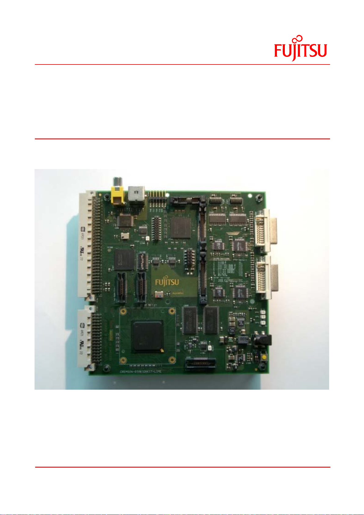
CREMSON-STARTERKITLIME Rev. 1.03
Lime Evaluation Board
Feb 2007
1.03
Revision 1.03 Page 1
© 2007 Fujitsu Microelectronics Europe
Page 2

MB86276 Evaluation Board Manual
Warranty and Disclaimer
To the maximum extent permitted by applicable law, Fujitsu Microelectronics Europe GmbH restricts its
warranties and its liability for Lime Evaluation Board and all its deliverables (e.g. software include or
header files, application examples, target boards, evaluation boards, engineering samples of IC’s etc.), its
performance and any consequential damages, on the use of the Product in accordance with (i) the terms of
the License Agreement and the Sale and Purchase Agreement under which agreements the Product has
been delivered, (ii) the technical descriptions and (iii) all accompanying written materials. In addition, to the
maximum extent permitted by applicable law, Fujitsu Microelectronics Europe GmbH disclaims all warranties
and liabilities for the performance of the Product and any consequential damages in cases of unauthorised
decompiling and/or reverse engineering and/or disassembling.
Note, the Lime Evaluation Board and all its deliverables are intended and must only be used in an
evaluation laboratory environment.
1. Fujitsu Microelectronics Europe GmbH warrants that the Product will perform substantially in
accordance with the accompanying written materials for a period of 90 days form the date of receipt
by the customer. Concerning the hardware components of the Product, Fujitsu Microelectronics
Europe GmbH warrants that the Product will be free from defects in material and workmanship under
use and service as specified in the accompanying written materials for a duration of 1 year from the
date of receipt by the customer.
2. Should a Product turn out to be defect, Fujitsu Microelectronics Europe GmbH’s entire liability and
the customer’s exclusive remedy shall be, at Fujitsu Microelectronics Europe GmbH’s sole
discretion, either return of the purchase price and the license fee, or replacement of the Product or
parts thereof, if the Product is returned to Fujitsu Microelectronics Europe GmbH in original packing
and without further defects resulting from the customer’s use or the transport. However, this warranty
is excluded if the defect has resulted from an accident not attributable to Fujitsu Microelectronics
Europe GmbH, or abuse or misapplication attributable to the customer or any other third party not
relating to Fujitsu Microelectronics Europe GmbH.
3. To the maximum extent permitted by applicable law Fujitsu Microelectronics Europe GmbH disclaims
all other warranties, whether expressed or implied, in particular, but not limited to, warranties of
merchantability and fitness for a particular purpose for which the Product is not designated.
4. To the maximum extent permitted by applicable law, Fujitsu Microelectronics Europe GmbH’s and its
suppliers´ liability is restricted to intention and gross negligence.
NO LIABILITY FOR CONSEQUENTIAL DAMAGES
To the maximum extent permitted by applicable law, in no event shall Fujitsu
Microelectronics Europe GmbH and its suppliers be liable for any damages whatsoever
(including but without limitation, consequential and/or indirect damages for personal injury,
assets of substantial value, loss of profits, interruption of business operation, loss of
information, or any other monetary or pecuniary loss) arising from the use of the Product.
Should one of the above stipulations be or become invalid and/or unenforceable, the remaining stipulations
shall stay in full effect
Page 2 of 18 Revision 1.03
© 2007 Fujitsu Microelectronics Europe
Page 3
MB86276 Evaluation Board Manual
Document Revision History
Revision Number Date Description of changes
1.00 25/10/05 Preliminary
1.01 06/01/06 First Version for Board Revision PA6
1.02 09/01/07 Added note for proprietary board designs and errata, general
information update and minor corrections
1.03 19/02/07 Corrected GMODE table
Evaluation Board Revision History
Revision Number Date Description of changes
PA5 30/11/05 First Board Version PA5
PA7 13/01/06 Revised version
- adds SW102 for Lime reset
- changes thermal pins to VCC18
Revision 1.03 Page 3 of 18
© 2007 Fujitsu Microelectronics Europe
Page 4

MB86276 Evaluation Board Manual
CONTENTS
Warranty and Disclaimer..................................................................................2
1 Overview.....................................................................................................5
2 MB86276 ‘Lime’ Features...........................................................................5
3 System Components ..................................................................................6
4 Layout and Interface Location ....................................................................7
5 Power Status LED’s....................................................................................8
6 Configuration DIP Switches ........................................................................9
6.1 CLKSEL0/CLKSEL1 ............................................................................10
6.2 CPU Mode ...........................................................................................10
6.3 General Purpose Mode Pins................................................................11
7 Interfaces and connectors ........................................................................12
7.1 Connectors between CPU board and graphic board ...........................12
7.2 Interface for the digital RGB output .....................................................15
7.3 Interface for LVDS out .........................................................................15
7.4 Interface for the digital RGB input........................................................16
7.5 Interface for the digital YUV422 input ..................................................16
8 Schematic Lime Evaluation Board (PA7)..................................................17
9 Important Notes for Proprietary Board Designs........................................17
10 Errata ........................................................................................................17
11 Worldwide Headquarters and Disclaimer..................................................18
Page 4 of 18 Revision 1.03
© 2007 Fujitsu Microelectronics Europe
Page 5

MB86276 Evaluation Board Manual
1 Overview
The CREMSON-STARTERKIT-LIME is a low-cost multifunctional evaluation board for Fujitsu’s
MB86276 ‘Lime’ Graphic Controller. The board is a part of a modular system and is connected to
the ‘CREMSON-STARTERKIT-CPU-Modul’ board as a simple target board for both software
development and testing, allowing design engineers to begin with software development
immediately before their proprietary (final) target system is available.
2 MB86276 ‘Lime’ Features
• CMOS 0.18μm technology
• Internal and memory frequency : 133MHz
• Base-clock for display clocks : 400.9MHz
• Display resolutions typically from 320x240
• 6 layers of overlay display (windows)
• Alpha Plane and constant alpha value
• Digital Video input (various formats
• Video Scaler (up/down scaling)
• Brightness, Contrast, Saturation control
• RGB digital output (8bit x 3)
• Built-in alpha blending, anti-aliasing
• Rendering Engine for various kinds
• Texture Mapping Unit for 2D polygon
• Bit-Blt Unit for transfers up to 4096x4096
• Alpha Bit-Blt and ROP2 functions
• External 32-bit SDRAM interface for
• Parallel host interface (FR, SH3, SH4)
• New additional serial control interface
• Internal and external DMA support
• I2C interface and GPIO inputs/outputs
• Supply voltage 3.3V (I/O), 1.8V (Internal)
• BGA-256 Package (1.27mm pitch)
• Typical power consumption < 1.0W
• Temperature range -40..+85 °C
Revision 1.03 Page 5 of 18
© 2007 Fujitsu Microelectronics Europe
Page 6
MB86276 Evaluation Board Manual
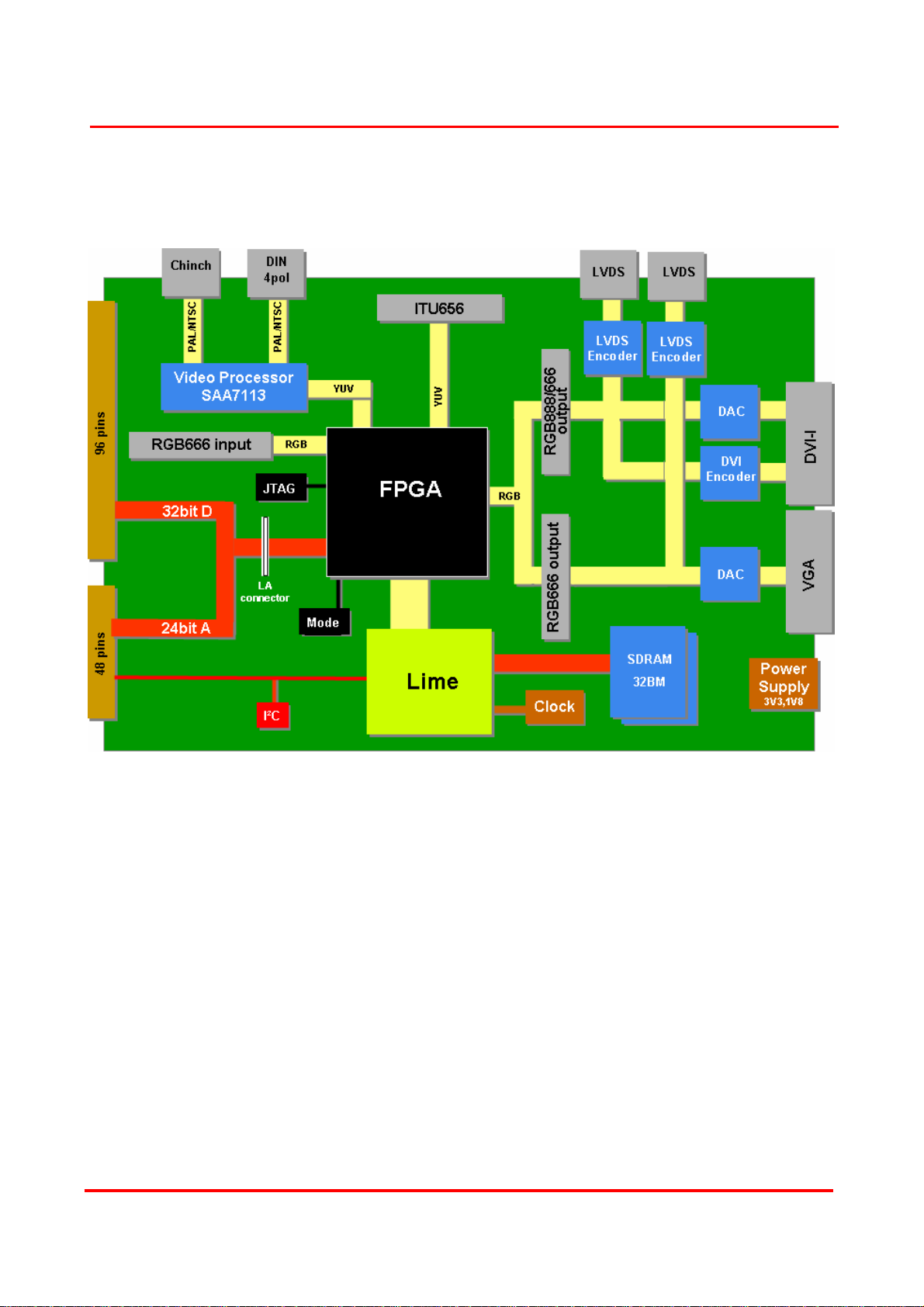
3 System Components
This diagram provides a functional overview of the system (note that it does not give a true
representation of the physical board – e.g. the FPGA device is actually two FPGA’s).
Figure 1 Functional Block Diagram
The main components and interfaces of the CREMSON-STARTERKIT-LIME evaluation board:
Lime Graphic Controller
64Mbytes SDRAM
Video outputs
o 2 x DVI
o 2 x RGB digital
o 2 x LVDS
Video inputs
o Digital RGB666
o Digital YUV422 (ITU656)
o CVBS
o S-Video
Others
o Xilinx FPGA’s
o Test LED’s
o Configuration settings
Page 6 of 18 Revision 1.03
© 2007 Fujitsu Microelectronics Europe
Page 7
MB86276 Evaluation Board Manual
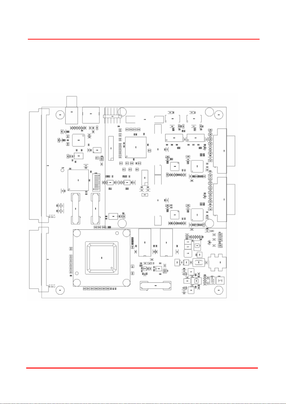
4 Layout and Interface Location
The location of the various interfaces of the board (the outline of which is shown below) is best
determined using the current schematics (in this document) and the physical board’s silkscreen
markings. Locate the connector’s ID (e.g. X703) in the schematics and then check the silkscreen
markings on the physical board.
Figure 1 Interfaces of the Lime evaluation board
Revision 1.03 Page 7 of 18
© 2007 Fujitsu Microelectronics Europe
Page 8
MB86276 Evaluation Board Manual
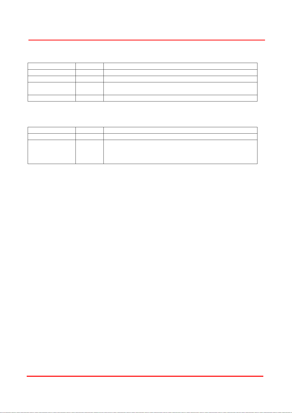
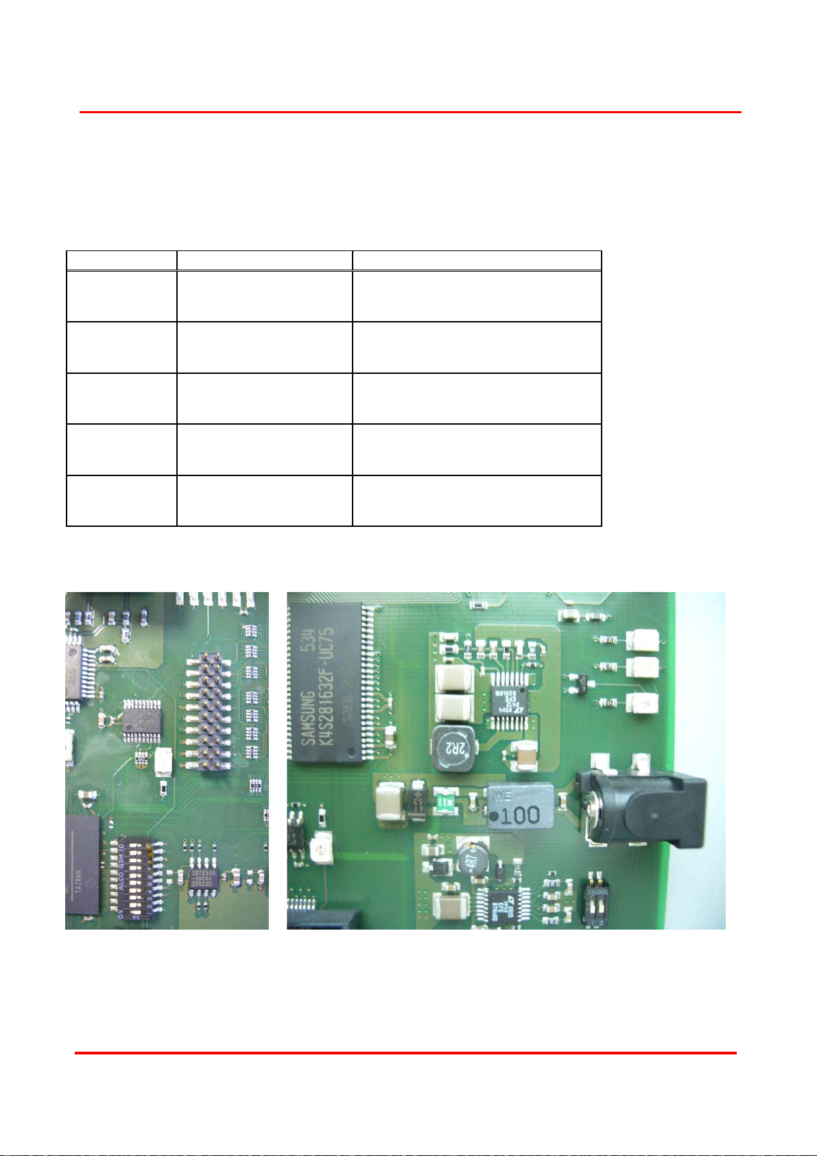
5 Power Status LED’s
LED’s are connected to the power nets of the board and therefore an illuminated LED shows the
availability of its corresponding power net. The power LED’s are located at the lower right corner of
the board, the Reset LED under the external SDRAM and the FPGA power LED near the video
input.
LED Function Description
D105
Reset
D106
1.8V supply
1.8V power supply
D107
3.3V supply
3.3V power supply
D108
5.0V supply
5.0V power supply
D700
3.3V supply
3.3V power supply
(Red)
Reset level active
(Green)
(Green)
(Green)
(Red)
Table 1 Power Status LED’s
Figure 2 Power Status LED's
Page 8 of 18 Revision 1.03
© 2007 Fujitsu Microelectronics Europe
Page 9
MB86276 Evaluation Board Manual
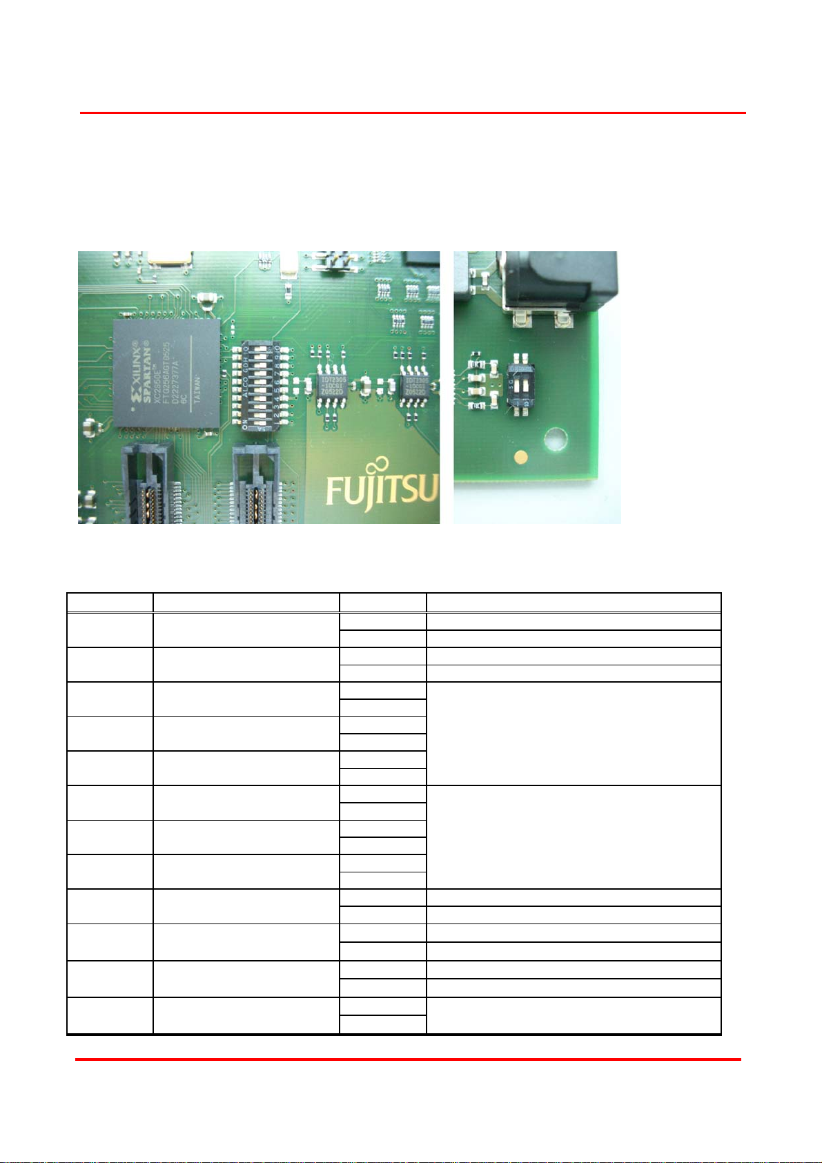
6 Configuration DIP Switches
The table shows DIP switches SW100 and SW101 of the Lime evaluation board. These should be
configured according to the intended host CPU interface mode and output display connection.
Before connecting the evaluation board for the first time, make sure that all switches are correctly
set. Possible settings and defaults are shown below.
Figure 3 Configuration DIP Switches
DIP switch Function Set Description
SW100-1 CLKSEL0
SW100-2 CLKSEL1
SW100-3 CPU MODE 0
SW100-4 CPU MODE 1
SW100-5 CPU MODE 2
SW100-6 MUX GMODE 0
SW100-7 MUX GMODE 1
SW100-8 MUX GMODE 2
SW100-9 BS Mode
SW100-10 RDY Mode
SW101-1
SW101-2 FPGA configuration
Switching Regulator
shutdown
ON Other oscillator settings
OFF 14.32 MHz source (Default)
ON 14.32 MHz source (Default)
OFF Other oscillator settings
ON
OFF
ON
OFF
ON
OFF
ON
OFF
ON
OFF
ON
OFF
ON Connects to CPU with BS signal
OFF Connects to CPU without BS signal
ON Sets the XRDY signal to the ‘not ready’ level
OFF Sets the XRDY signal to the ‘ready’ level
ON Switch On
OFF Switch Off
ON
OFF
Host CPU mode select¹
General purpose mode pins²
Reserved
Revision 1.03 Page 9 of 18
© 2007 Fujitsu Microelectronics Europe
Page 10

MB86276 Evaluation Board Manual
¹,² Check the CPU mode and the General Purpose Mode tables in the hardware manual (see also below).
For Hardware Manual cross-reference purposes: (see following sections)
ON = Low
OFF = High
6.1 CLKSEL0/CLKSEL1
The following table (copied from the MB86276 ‘Lime’ Hardware Manual available at the time this
document was written) lists the CLKSEL settings that can be selected.
CLKSEL1 CLKSEL0 Input frequency Assured operation range (*
L L 13.5 MHz 13.365 to 13.5 MHz
L H 14.32 MHz 14.177 to 14.32 MHz
H L 17.73 Hz 17.553 to 17.73 MHz
H H 33.33 Hz 32.997 to 33.33 MHz
1
)
Table 2 Clock Select
*1 Assured operation input frequency range: Standard value –1%
6.2 CPU Mode
The following table (copied from the MB86276 ‘Lime’ Hardware Manual available at the time this
document was written) lists the CPU modes that can be selected.
CPU MODE 2 CPU MODE 1 CPU MODE 0 CPU
L L
L L
L H
L H H SPARClite
H L L General purpose 16bit CPU with SRAM interface
H L H
H H L
H H H I2C Slave
L SH3 (Fujitsu FR series MCU’s)
H SH4
L V832
General purpose 16bit CPU with address and data multiplex
interface
General-purpose 32bit CPU with address and data multiplex
interface
Table 3 CPU Modes
Page 10 of 18 Revision 1.03
© 2007 Fujitsu Microelectronics Europe
Page 11

MB86276 Evaluation Board Manual
6.3 General Purpose Mode Pins
The following table (copied from the MB86276 ‘Lime’ Hardware Manual available at the time this
document was written, talking the Errata Sheet nto consideration) lists the General Purpose modes
that can be selected and the pin multiplex functionality that results (note also the dependency on
the corresponding CPU mode listed in the previous section).
MUX
GMODE
2
L L
L L
L H
L H H
H L L Reserved Reserved Reserved Reserved Reserved
H L H Reserved Reserved Reserved Reserved Reserved
H H L Reserved Reserved Reserved Reserved Reserved
H H H Reserved Reserved Reserved Reserved Reserved
MUX
GMODE
1
MUX
GMODE
0
Host Interface
L
H
L
32bit CPU
I2C Slave
32bit CPU
I2C Slave
16bit CPU
I2C Slave
16bit CPU
I2C Slave
Primary
RGB output
RGB888 --
RGB888 -- RBT656/601 GPIO[4:0]
RGB666 RGB888 RBT656/601 GPIO[2:0]
RGB666 RGB666
PIN Multiplex
Secondary
RGB output
Video
Capture
Native
RGB666
Native
RGB666
GPIO
--
--
Table 4 Multiplex Modes
Revision 1.03 Page 11 of 18
© 2007 Fujitsu Microelectronics Europe
Page 12

MB86276 Evaluation Board Manual
7 Interfaces and connectors
7.1 Connectors between CPU board and graphic board
This section describes the connector allocation between the CPU board and the graphic board.
The connection of the two sub-boards is realized by two connectors: a 96-pole DIN plug and a 48pole DIN plug.
Figure 3 Connection Block Diagram
Page 12 of 18 Revision 1.03
© 2007 Fujitsu Microelectronics Europe
Page 13

MB86276 Evaluation Board Manual
Pin Name Pin Name Pin Name
A1 n.c. B1 n.c. C1 n.c.
A2 3.3V B2 3.3V C2 3.3V
A3 5.0V B3 5.0V C3 5.0V
A4 GND B4 GND C4 GND
A5 D0 B5 D1 C5 D2
A6 D3 B6 D4 C6 D5
A7 D6 B7 D7 C7 D8
A8 D9 B8 D10 C8 D11
A9 D12 B9 D13 C9 D14
A10 D15 B10 D16 C10 D17
A11 D18 B11 D19 C11 D20
A12 D21 B12 D22 C12 D23
A13 D24 B13 D25 C13 D26
A14 D27 B14 D28 C14 D29
A15 D30 B15 D31 C15 GND
A16 GND B16 GND C16 GND
A17 A0 B17 A1 C17 A2
A18 A3 B18 A4 C18 A5
A19 A6 B19 A7 C19 A8
A20 A9 B20 A10 C20 A11
A21 A12 B21 A13 C21 A14
A22 A15 B22 A16 C22 A17
A23 A18 B23 A19 C23 A20
A24 A21 B24 A22 C24 A23
A25 A24 B25 A25 C25 n.c.
A26 n.c. B26 n.c. C26 n.c.
A27 n.c. B27 n.c. C27 GND
A28 S0 B28 S1 C28 S2
A29 S3 B29 S4 C29 S5
A30 S6 B30 S7 C30 GND
A31 n.c. B31 n.c. C31 n.c.
A32 GND B32 GND C32 GND
Table 5 96-Pole Connector Pin*¹ Reference
Revision 1.03 Page 13 of 18
© 2007 Fujitsu Microelectronics Europe
Page 14

MB86276 Evaluation Board Manual
Pin Name Pin Name Pin Name
A1 CS0 B1 GND C1 CS1
A2 CS2 B2 1.8V C2 CS3*
A3 CS4 B3 GND C3 CS5
A4 CS6 B4 1.8V C4 RDY
A5 BGRNT B5 GND C5 BRQ
A6 RDX B6 n.c. C6 WR0
A7 WR1 B7 n.c. C7 WR2
A8 WR3 B8 n.c. C8 AS
A9 ALE B9 n.c. C9 CLK
A10 DREQ0 B10 n.c. C10 DACK0
A11 DEOP0 B11 n.c. C11 n.c.
A12 IRQ_A B12 n.c. C12 SDA
A13 IRQ_B B13 n.c. C13 SCL
A14 SIN B14 n.c. C14 SOT
A15 GND B15 n.c. C15 SLK
A16 RESET B16 n.c. C16 GND
2
Table 6 48-Pole Connector Pin*¹ Reference
*¹ Note:
The pin number refers to the female connector of the CPU main board.
*2 Note:
CS3: This is currently used by the FR 467 and 369 CPU’s in connection with the Lime device.
Page 14 of 18 Revision 1.03
© 2007 Fujitsu Microelectronics Europe
Page 15

MB86276 Evaluation Board Manual
7.2 Interface for the digital RGB output
Figure 6 Digital RGB out
7.3 Interface for LVDS out
Figure 7 LVDS out
Revision 1.03 Page 15 of 18
© 2007 Fujitsu Microelectronics Europe
Page 16

7.4 Interface for the digital RGB input
Figure 8 Digital RGB in
7.5 Interface for the digital YUV422 input
MB86276 Evaluation Board Manual
Figure 9 Digital YUV422 (ITU656) input
RGB digital input
Page 16 of 18 Revision 1.03
© 2007 Fujitsu Microelectronics Europe
Page 17

MB86276 Evaluation Board Manual
8 Schematic Lime Evaluation Board (PA7)
Please refer to the pages following the Fujitsu Headquarters address information.
9 Important Notes for Proprietary Board Designs
Address line remapping via FPGA
Customers who wish to use Lime in legacy 32-bit modes (SH3, SH4, V832, and FR) and
may want to simplify the situation by directly mapping Lime's host interface to the host
interface connector should be aware that the FPGA on the Starterkit maps the CPU’s
address bus lines to those of the Lime device with an offset according to the CPU type.
For 16 bit CPU’s the offset is 1 (i.e. line 1 of the address bus is mapped to line 0 of Lime).
For 32 bit CPU’s the offset is 2 (i.e. line 2 of the address bus is mapped to line 0 of Lime).
Direct Access to Graphics Memory
If you are trying to access Lime on the Starterkit board from your own CPU board, direct
access to graphics memory can be very critical in verifying CPU-Lime communication. Also,
if you want to use Local Memory Transfer of display lists to store bitmaps in graphics
memory etc. direct access to the Graphics Memory is necessary. This requires modified
FPGA firmware which can be obtained by contacting the GCC Application Group
(
gdc_info@fme.fujitsu.com).
Using a non-Fujitsu CPU board / Component Initialization via I2C
I2C master communication using the Lime device is not possible for the slave devices
SAA7113 and DVI Panel Link Translator. These slave devices should therefore be
initialized through I2C using the host interface (i.e. the MCU must control the peripheral
directly).
10 Errata
Incorrect silkscreen board markings/comments in schematics
The silkscreen description and schematic comments for the settings of SW100 are
incorrect for the PA7 version of the board. The table lists the default settings as follows:
CLKSEL0 Default ON
CLKSEL1 Default OFF
The correct settings are: (14.32 MHz)
CLKSEL0 Default OFF
CLKSEL1 Default ON
Revision 1.03 Page 17 of 18
© 2007 Fujitsu Microelectronics Europe
Page 18

MB86276 Evaluation Board Manual
11 Worldwide Headquarters and Disclaimer
Japan
Tel: +81 3 5322 3353
Fax: +81 3 5322 3386
Fujitsu Limited
Shinjuku Dai-Ichi Seimei
Bldg. 2-7-1, Nishi-shinjuku
Shinjuku-ku,
Tokyo 163-0721
Japan
Asia Pacific
Tel: +65 281 0770
Fax: +65 281 0220
http://www.fujitsu.com http://www.fujitsu.com/sg/
USA
Tel: +1 408 737-5600
Fax: +1 408 737-5999
http://www.fujitsu.com/us/services/edevices/microelectr
onics/
Fujitsu Microelectronics
America Inc.
1250 E. Arques Avenue, M/S
333, Sunnyvale, CA
USA
94088-3470
Customer Response Center
Mon-Fri 7am-5pm (PST)
Europe
Tel: +49 6103 6900
Fax:+49 6103 690122
http://www.fujitsu.com/emea/services/microelectronics/
The contents of this document are subject to change without notice. Customers are advised to consult with FUJITSU sales
representatives before ordering.
The information and circuit diagrams in this document are presented as examples of semiconductor device applications, and are
not intended to be incorporated in devices for actual use. Also, FUJITSU is unable to assume responsibility for infringement of
any patent rights or other rights of third parties arising from the use of this information or circuit diagrams. No license is granted
by implication or otherwise under any patent or patent rights of Fujitsu Microelectronics GmbH.
FUJITSU semiconductor devices are intended for use in standard applications (computers, office automation and other office
equipment, industrial, communications and measurement equipment, personal or household devices, etc.).
CAUTION: Customers considering the use of our products in special applications where failure or abnormal operation may
directly affect human lives or cause physical injury or property damage, or where extremely high levels of reliability are demanded
(such as aerospace systems, atomic energy controls, sea floor repeaters, vehicle operating controls, medical devices for life
support, etc.) are requested to consult with FUJITSU sales representatives before such use. The company will not be responsible
for damages arising from such use without prior approval.
Any semiconductor devices have inherently a certain rate of failure. You must protect against injury, damage or loss from such
failures by incorporating safety design measures into your facility and equipment such as redundancy, fire protection, and
prevention of over-current levels and other abnormal operating conditions.
If any products described in this document represent goods or technologies subject to certain restrictions on export under the
Foreign Exchange and Foreign Trade Control Law of Japan, the prior authorisation by Japanese government should be required
for export of those products from Japan.
Fujitsu Microelectronics Asia Ltd
151 Lorong Chauan
New Tech Park #05-08
Singapore 556741
Fujitsu Microelectronics Europe GmbH
Pittlerstrasse 47
D-63225 Langen
Germany
Page 18 of 18 Revision 1.03
© 2007 Fujitsu Microelectronics Europe
Page 19

5
4
3
2
1
Power &
D D
Config
FPGA_CFG
EXT_RESET#
FPGA_CFG
EXT_RESET#
CONFIG[9..0]
RESET#[1..0]
#2Reference ID: 100
CONFIG[9..0]
RESET#[1..0]
RESET#1
Lime Evaluation Board
Revision: PA8
EXT_RESET#
C C
RESET#1
RESET#1
Video
FPGA_CFG
Lime Subsystem
Input
I2C[1..0]
VI_656_CLK
B B
Reference ID: 200 #4#8
VI_656_D[7..0]
Lime Evaluation Board
Hierarchy Part References
+---#1 Lime Eval Top
¦
+---#2 Power 1xx
+---#3 Video Input 2xx
+---#4 Video Output
+---#5 RGB Output 3xx
+---#6 DVI Output 4xx
+---#7 LVDS Output 5xx
+---#8 Lime Subsystem
+---#9 Lime 6xx
A A
+---#10 FPGA 7xx
+---#11 DRAM 8xx
5
I2C[1..0]
VI_656_CLK
I2C[1..0]
VI_656_CLK
VI_656_D[7..0] VO1_RGB[23..0]
Top
I2C Address Map
Device Function
Ux00 SAA7113 composite video input 0x48 0x49
Ux00 XC2S200E* video input selector 0x60 0x61
and host CPU bus mux
Ux00 SIL164 DVI transmitter #0 0x70 0x71
Ux01 SIL164 DVI transmitter #1 0x72 0x73
* I2C address of video input selector depends on
FPGA implementation
4
3
RESET#[1..0]
CONFIG[9..0]
VO0_SYNC[4..0]
VO1_SYNC[4..0]
VO0_CLK[3..0]
VO1_CLK[3..0]
VO0_RGB[23..0]
ReadWrite
2
RESET#1
I2C[1..0]
VO0_SYNC[4..0]
VO1_SYNC[4..0]
VO0_CLK[3..0]
VO1_CLK[3..0]
VO0_RGB[23..0]
VO1_RGB[23..0]VI_656_D[7..0]
RESET#1
I2C[1..0]
Video
Output
VO0_SYNC[4..0]
VO1_SYNC[4..0]
VO0_CLK[3..0]
VO1_CLK[3..0]
VO0_RGB[23..0]
VO1_RGB[23..0]
Top#3
© mycable GmbH
Boeker Stieg 43
D-24613 Aukrug
Germany
www.mycable.de
Title
Fujitsu Lime Evaluation Board
Size Document Number Re v
30200-001 PA8
A3
Date: Sheet of
111Tuesday, December 12, 2006
1
Page 20

5
4
3
2
1
VCC50
C105
10u
C114
10u
309kR109
110kR116
D102
CMDSH-3
L101 744773047
C108
10u 1812
L102 744773033
D103
CMDSH-3
PCB layout: refer to
application note!
U101
16
PVIN2
9
PVIN1
1
SVIN
5
RT
7
RUN/SS
3
ITH
6
SYNC/MODE
4
VFB
LTC3412EFE
SGND2
17
PGOOD
PGND1
PGND2
SGND1
SW1
SW2
SW3
SW4
C103
100n 0603
C109
100n 0603
C112
100n 0603
2
10
11
14
15
12
13
8
PG_VCC18
PCB layout: refer to
application note!
R100 30k1
D101
MBRM120LT3
U100
1
BOOST1
2
SW1
3
VIN1
4
VIN2
5
VIN3
6
VIN4
7
SW2
8
BOOST2
LT1940EFE
D104
MBRM120LT3
VCC33
10kR107
L103
7447785002
R115
232k
LT1940
GND
UM
R106 16k5
C115
22p
RUN/SS1
RUN/SS2
DIP Switch Settings
1 CLKSEL0 on
2 CLKSEL1 off
3 Host CPU MODE 0 n/a
4 Host CPU MODE 1 n/a
5 Host CPU MODE 2 n/a
6 Pin mux GMODE0 n/a
7 Pin mux GMODE1 n/a
8 Pin mux GMODE2 n/a
9 BS Mode n/a
10 RDY Mode n/a
n/a: settings depen d on the corresponding host CPU
interface mode and display connection
1 1940 shutdown off
2 FPGA user config n/a
If 3.3V and 5V is provided by the host CPU board, both
regulators must be shut down. No wall pow er supply
shall be conne cted to the Lime board in this case.
CONFIG[9..0]
FPGA_CFG
RESET#[1..0]
RESET#0
RESET#1
PCB label:
3.3V
R112
470R
D107
TLMC3100
PCB label:
5.0V
VCC50VCC33VCC33 VCC33VCC18
R113
680R
D108
TLMC3100
CONFIG[9..0]
FPGA_CFG
RESET#[1..0]
SW101
506-GDH02S
FPGA_CFG
SD33#
R125
10k
PCB label:
RESET
PCB label:
Config
SW100
506-GDH10S
CONFIG3
CONFIG0
CONFIG2
CONFIG1
CONFIG4
R110
390R
D105
TLMT3100
CONFIG5
CONFIG6
CONFIG7
CONFIG8
CONFIG9
PCB label:
PG 1.8V
Config
switch #no function default
Supply
switch #no function default
R111
470R
D106
TLMC3100
PCB label:
R101
10k
R102 0R
16
FB1
15
VC1
14
PG1
13
12
11
PG2
10
VC2
9
FB2
C116
100n
R103 15k
SD33#
R104 15k
C117
100u
C106 330p
C107 1n 0603
C110 1n 0603
C111 330p
R105
10k
C118
100u
Supply
VCC33
D100
SMAJ18A
15kR114
C123
100p
Place Cs close to
power input!
+
C100
100u
C104
100n
VCC33
C113
100n
R117
75k
VCC_EXT
L100
X100
1
2
3
D D
C C
KLD-SMT2-0202-A
VCC50
744226
C101
1n 0603
2 1
C120
C119
100n
C121
22u
1n
F100
microSMD110
C102
1n 0603
3 4
R108
4M7
C122
1n
RESET#1
B B
VCC50 VCC33VCC33VCC18 VCC33 VCC33VCC33
Place C126 - C130 directly to
R118
4k7
RESET#0
C127
100n
U104
OE
A
GND
NC7SZ125
R126 110k
NC7SZ125
C128
10n
5
VCC
4
Y
C126
100n
A A
EXT_RESET#
EXT_RESET#
5
1
2
3
the corresponding U102 pins!
U102
1
2
3
4
5
R127 470R
VCC33
4
V3
V1
CRT
RST#
PBR#
LTC2900-1IMS
C131
100n
LTC2900
1 4
2 3
V2
V4
VREF
VPG
GND
SW102
B3S1000
R119
4k7
10
9
8
7
6
9k53R121
C129
R122
R123
93k1
4k7
C130
100n
100n
3
R120
4k7
RESET#0
U103
1
CONTROL
2
RESIN
3
CT
4
GND
C125
100n
TLC7733ID
TLC7733
PG_VCC18
SENSE
RESET
RESET#
RESET#1
T100
MGSF1N02LT1
8
VDD
7
6
5
2
C124
100n
4k7R124
© mycable GmbH
Boeker Stieg 43
D-24613 Aukrug
Germany
www.mycable.de
Title
Fujitsu Lime Evalua tion Board: Power
Size Document Number Rev
A2
30200-002 PA8
Date: Sheet
1
211Tuesday, December 12, 2006
of
Page 21

5
4
3
2
1
VI_656_D[7..0]
D D
I2C[1..0]
VI_656_CLK
C C
VI_656_D[7..0]
I2C[1..0]
VI_656_CLK
VI_656_D0
VI_656_D1
VI_656_D2
VI_656_D3
VI_656_D4
VI_656_D5
VI_656_D6
VI_656_D7
I2C1 I2C_SDA
I2C0 I2C_SCL
RN200
1
2
3
4 5
33Rx4
RN201
1
2
3
4 5
33Rx4
R202
33R
8
7
6
8
7
6
SAA7113_CLK
Place RN300, RN301 and
R304 directly to the
corresponding U300 pins!
RESET#1
RESET#1
I2C addresses of SAA7113
read: 0x49, write: 0x48
PCB Layout: refer to layout guide
and SAA7113 application note!
U200
Video out
22
VPO0
21
VPO1
20
VPO2
19
VPO3
15
VPO4
14
VPO5
13
VPO6
12
VPO7
23
SDA
24
SCL
31
XTAL
32
XTALI
17
LLC
SAA7113H
I2C
Clock
IO
RTS026RTS127RTC025VDDA010VSSA0
11CE40
Video in 1
Video in 2
Boundary
Scan
35
4k7R203
AI11
AI1D
AI12
AOUT
AI21
AI2D
AI22
AGND
VSSA1
VSSA2
VDDA1
VDDA2
TCK
TMS
TRST
TDO
VDDDE118VDDDI29VDDDA33VDDDE234VSSDE116VSSDI28VSSDA30VSSDE2
JEITA RC-5231
4
5
VI_AI12
7
9
43
44
VI_AI22
1
6
2
41
3
42
38
TDI
37
39
8
36
C205
1n
C201
47n
C204
100n
GND_CV
C206
100n
C202
47n
C200
47n
R201
56R
C203
47n
GND_CVGND_CV GND_CV
VCC33
L200
BLM18PG600SN1
C207
Place filter network
10u
directly to VDDAx and
R200
18R
1
GND_CV
X200
2
VSSAx power pins!
GND_CV
VCC33
Keep SAA7113 clock signal
as short as possible!
B B
C212
1u
SAA7113_CLK
C213
100n
33RR205
L201
BLM18PG600SN1
Y200
4
VCC
OSC
3
OUT
SG8002 CA PC 24.576
GND
1
OE
2
Place R205 directly
to Y200 pin 3!
L303
A A
5
BLM18PG600SN1
GND_CV
New
4
R204
10k
VCC33
C214
100n
VI_AI12
VI_AI22
GND_CV
C215
47n
47n
C216
L202
BLM18PG600SN1
R207
56R
GND_CV
R209
56R
GND_CV
3
R206
18R
R208
18R
GND_CV
C208
C209
1n
100n
X201
MDIN04SSV-BC
4
2 1
567
3
C210
100n
GND_CV
C211
10u
2
Place capacitors directly
to digital power pins!
© mycable GmbH
Boeker Stieg 43
D-24613 Aukrug
Germany
www.mycable.de
Title
Fujitsu lime Evaluation Boa rd: Video Input
Size Document Number Re v
30200-003 PA8
A3
Date: Sheet of
311Tuesday, December 12, 2006
1
Page 22

5
D D
4
3
2
1
RESET#1
RESET#1
DVI Output
VO0_CLK2
I2C[1..0]
RESET#1
C C
VO0_RGB[23..0]
VO1_RGB[23..0]
I2C[1..0]
RESET#1
VO0_RGB[23..0]
VO1_RGB[23..0]
RESET#1
RGB Output
I2C[1..0]
VO0_RGB[23..0]
VO1_RGB[23..0]
VO0_RGBAN[2..0]
VO1_RGBAN[2..0]
VO0_CLK[1..0]
VO0_SYNC[4..0]
VO1_CLK[1..0]
VO1_SYNC[4..0]
#5 Reference ID: 300
VO0_SYNC[4..0]
VO1_SYNC[4..0]
B B
VO1_CLK[3..0]
VO0_CLK[3..0]
VO0_SYNC[4..0]
VO1_SYNC[4..0]
VO1_CLK[3..0]
VO1_CLK0
VO1_CLK1
VO1_CLK2
VO1_CLK3
VO0_CLK[3..0] VO0_CLK[1..0]
VO1_CLK[1..0]
VO1_CLK2
VO0_RGB[23..0]
VO1_RGB[23..0]
VO0_RGBAN[2..0]
VO1_RGBAN[2..0]
VO0_SYNC[2..0]
VO1_SYNC[2..0]
VO1_SYNC0
VO1_SYNC1
VO1_SYNC2
VO1_SYNC0
VO1_SYNC1
VO1_SYNC2
VO1_SYNC3
RESET#1
VO0_SYNC0
VO0_SYNC1
VO0_SYNC2
VO0_CLK3
VO1_CLK3
VO0_SYNC0
VO0_SYNC1
VO0_SYNC2
VO0_SYNC3
VO0_SYNC[3..0]
VO1_SYNC[3..0]
VO0_RGB[23..0]
VO1_RGB[23..0]
VO0_CLK2
VO1_CLK2
I2C[1..0]
VO0_RGB[23..0]
VO1_RGB[23..0]
VO0_RGBAN[2..0]
VO1_RGBAN[2..0]
VO0_SYNC[2..0]
VO1_SYNC[2..0]
#6 Reference ID: 400
RESET#1
LVDS Output
VO0_CLK3
VO1_CLK3
VO0_SYNC[3..0]
VO1_SYNC[3..0]
VO0_RGB[23..0]
VO1_RGB[23..0]
Reference ID: 500#7
VO0_CLK0
VO0_CLK1
VO0_CLK2
VO0_CLK3
A A
5
4
3
2
© mycable GmbH
Boeker Stieg 43
D-24613 Aukrug
Germany
www.mycable.de
Title
Fujitsu Lime Evaluation Boa rd: Video Output
Size Document Number Re v
30200-004
A3
Date: Sheet of
411Tuesday, December 12, 2006
1
PA8
Page 23

5
4
3
2
1
VCC33 VCC33
D D
VO1_RGB[23..0]
VO0_RGB[23..0]
VO0_CLK[1..0]
VO1_CLK[1..0]
C C
I2C[1..0]
RESET#1
VO0_SYNC[4..0]
VO1_SYNC[4..0]
B B
VO1_RGB[23..0]
VO0_RGB[23..0]
VO0_CLK[1..0]
VO0_CLK0
VO0_CLK1
VO1_CLK[1..0]
VO1_CLK0
VO1_CLK1
I2C[1..0]
RESET#1
VO0_SYNC[4..0]
VO1_SYNC[4..0]
VO1_SYNC0 VO1_HSYNC
VO1_SYNC1 VO1_VSYNC
VO1_SYNC2 VO1_DE
VO1_SYNC3 VO1_CSYNC
VO1_SYNC4 VO1_GV
Place filter network directly
to U500 power pins!
L300
BLM18PG600SN1
VO0_SYNC3 VO0_CSYNC
VO0_SYNC4 VO0_GV
C300
10u
VO0_RGB0 VO0_B0
VO0_RGB1 VO0_B1
VO0_RGB2 VO0_B2
VO0_RGB3 VO0_B3
VO0_RGB4 VO0_B4
VO0_RGB5 VO0_B5
VO0_RGB6 VO0_B6
VO0_RGB7 VO0_B7
VO0_RGB8 VO0_G0
VO0_RGB9 VO0_G1
VO0_RGB10 VO0_G2
VO0_RGB11 VO0_G3
VO0_RGB12 VO0_G4
VO0_RGB13 VO0_G5
VO0_RGB14 VO0_G6
VO0_RGB15 VO0_G7
VO0_RGB16 VO0_R0
VO0_RGB17 VO0_R1
VO0_RGB18 VO0_R2
VO0_RGB19 VO0_R3
VO0_RGB20 VO0_R4
VO0_RGB21 VO0_R5
VO0_RGB22 VO0_R6
VO0_RGB23 VO0_R7
VO0_CSYNC
VO0_CLK0 VO1_CLK0
VCC33
RESET#1 RESET#1
I2C0 I2C_SCL
I2C1 I2C_SDA
VO0_SYNC0 VO0_HSYNC
VO0_SYNC1 VO0_VSYNC
VO0_SYNC2 VO0_DE
NP
C302
C301
100n
10kR310
0RR312
10kR314
0RR316
C303
100n
1n
30
U300
VCC13VCC29VCC
16
B0
17
B1
18
B2
19
B3
20
B4
21
B5
22
B6
23
B7
3
G0
4
G1
5
G2
6
G3
7
G4
8
G5
9
G6
10
G7
41
R0
42
R1
43
R2
44
R3
45
R4
46
R5
47
R6
48
R7
12
SYNC#
11
BLANK
24
CLOCK
38
PSAVE#
ADV7125JSTZ240
GND1GND2GND14GND15GND25GND26GND39GND
ADV7125
Video DAC
Consider ADV7125 layout rules!
40
COMP
VREF
RSET
IOR#
IOG#
IOB#
GND_RGBO
IOR
IOG
IOB
34
32
28
33
31
27
GND_RGBO
35
36
37
VO0_B0
VO0_B2
VO0_B4
VO0_B6
VO0_G0
VO0_G2
VO0_G4
VO0_G6
VO0_R0
VO0_R2
VO0_R4
VO0_R6
VO0_HSYNC
VO0_DE
VO0_GV
I2C_SCL
C308
100n
R300
75R
C309
100n
68RR306
L302
BLM18PG600SN1
1 2
3 4
5 6
7 8
9 10
11 12
13 14
15 16
17 18
19 20
21
23 24
25
27 28
29 30
31 32
33 34
35 36
37 38
39 40
FTSH-120-01-L-DV-EJ-P
VO1_RGB[23..0]
VO0_RGBAN2
VO0_RGBAN1
VO0_RGBAN0
R302
R301
75R
75R
NP
100nC312
470RR307
GND_RGBO
GND_RGBO
X300
VO0_B1
VO0_B3
VO0_B5
VO0_B7
VO0_G1
VO0_G3
VO0_G5
VO0_G7
22
VO0_R1
VO0_R3
26
VO0_R5
RGB digital output #0
VO0_R7
VO0_VSYNC
VO0_CSYNC
VO0_CLK1
I2C_SDA
100nC314
VCC33 VCC33
10uC315
VO1_B0
VO1_B2
VO1_B4
VO1_B6
VO1_G0
VO1_G2
VO1_G4
VO1_G6
VO1_R0
VO1_R2
VO1_R4
VO1_R6
VO1_HSYNC
VO1_DE
VO1_GV
I2C_SCL
Place filter network directly
to U501 power pins!
L301
BLM18PG600SN1
VCC33
10u
1 2
3 4
5 6
7 8
9 10
11 12
13 14
15 16
17 18
19 20
21
23 24
25
27 28
29 30
31 32
33 34
35 36
37 38
39 40
FTSH-120-01-L-DV-EJ-P
C304
C305
100n
VO1_RGB0 VO1_B0
VO1_RGB1 VO1_B1
VO1_RGB2 VO1_B2
VO1_RGB3 VO1_B3
VO1_RGB4 VO1_B4
VO1_RGB5 VO1_B5
VO1_RGB6 VO1_B6
VO1_RGB7 VO1_B7
VO1_RGB8 VO1_G0
VO1_RGB9 VO1_G1
VO1_RGB10 VO1_G2
VO1_RGB11 VO1_G3
VO1_RGB12 VO1_G4
VO1_RGB13 VO1_G5
VO1_RGB14 VO1_G6
VO1_RGB15 VO1_G7
VO1_RGB16 VO1_R0
VO1_RGB17 VO1_R1
VO1_RGB18 VO1_R2
VO1_RGB19 VO1_R3
VO1_RGB20 VO1_R4
VO1_RGB21 VO1_R5
VO1_RGB22 VO1_R6
VO1_RGB23 VO1_R7
VO1_CSYNC
10kR311
0RR313
10kR315
0RR317
NP
X301
22
26
RGB digital output #1
100nC316
10uC317
C306
100n
VO1_B1
VO1_B3
VO1_B5
VO1_B7
VO1_G1
VO1_G3
VO1_G5
VO1_G7
VO1_R1
VO1_R3
VO1_R5
VO1_R7
VO1_VSYNC
VO1_CSYNC
VO1_CLK1
I2C_SDA
C307
1n
U301
16
B0
17
B1
18
B2
19
B3
20
B4
21
B5
22
B6
23
B7
3
G0
4
G1
5
G2
6
G3
7
G4
8
G5
9
G6
10
G7
41
R0
42
R1
43
R2
44
R3
45
R4
46
R5
47
R6
48
R7
12
SYNC#
11
BLANK
24
CLOCK
38
PSAVE#
ADV7125JSTZ240
30
VCC13VCC29VCC
GND1GND2GND14GND15GND25GND26GND39GND
ADV7125
Video DAC
GND_RGBO
40
34
IOR
32
IOG
28
IOB
33
IOR#
31
IOG#
27
IOB#
GND_RGBO
35
COMP
36
VREF
37
RSET
VO1_RED VO1_RGBAN2
VO1_RGBAN2
VO1_RGBAN1
VO1_RGBAN0
R304
R305
R303
75R
75R
75R
C310
C311
100n
100n
NP
100nC313
68RR308
470RR309
GND_RGBO
VO0_RGBAN[2..0]
VO1_RGBAN[2..0]
VO0_RGBAN0VO0_BLUE
VO0_RGBAN1VO0_GREEN
VO0_RGBAN2VO0_RED
VO1_RGBAN0VO1_BLUE
VO1_RGBAN1VO1_GREEN
VO0_RGBAN[2..0]
VO1_RGBAN[2..0]
A A
© mycable GmbH
Boeker Stieg 43
D-24613 Aukrug
Germany
www.mycable.de
Title
Fujitsu Lime Evaluation Board: Video Output: RGB Output
Size Document Number Rev
A2
30200-005
5
4
3
2
Date: Sheet
1
511Tuesday, December 12, 2006
PA8
of
Page 24

5
4
3
2
1
VO0_RGB[23..0]
VO0_SYNC[2..0]
D D
VO0_RGBAN[2..0]
VO0_CLK2
RESET#1
C C
VO1_RGB[23..0]
VO1_SYNC[2..0]
VO1_RGBAN[2..0]
B B
VO1_CLK2
I2C[1..0]
A A
VO0_RGB[23..0]
VO0_SYNC[2..0]
VO0_RGBAN[2..0]
VO0_CLK2
RESET#1
I2C addresses of SIL164 #0
read: 0x71, write: 0x70
VO1_RGB[23..0]
VO1_SYNC[2..0]
VO1_RGBAN[2..0]
VO1_CLK2
I2C[1..0]
I2C addresses of SIL164 #1
read: 0x73, write: 0x72
5
VO0_SYNC0 VO0_HSYNC
VO0_SYNC1 VO0_VSYNC
VO0_SYNC2 VO0_DE
VO0_RGBAN0 VO0_BLUE
VO0_RGBAN1 VO0_GREEN
VO0_RGBAN2 VO0_RED
VCC33
7
8
7
8
VO1_SYNC0 VO1_HSYNC
VO1_SYNC1 VO1_VSYNC
VO1_SYNC2 VO1_DE
VO1_RGBAN0 VO1_BLUE
VO1_RGBAN1 VO1_GREEN
VO1_RGBAN2 VO1_RED
VCC33
7
8
I2C0 I2C_SCL
I2C1 I2C_SDA
RESET#1
RN400
4k7x4
RN401
4k7x4
RN402
4k7x4
VO0_RGB0 VO0_B0
VO0_RGB1 VO0_B1
3456
2
1
3456
DVI1_PD
2
DVI1_ISEL
1
0RR404
0RR405
0RR406
0RR407
0RR409
VO1_RGB1 VO1_B1
VO1_RGB0 VO1_B0
3456
2
1
0RR414
0RR415
0RR416
0RR417
0RR419
L416
BLM18PG600SN1
VO0_RGB2 VO0_B2
VO1_RGB2 VO1_B2
VO0_RGB3 VO0_B3
VO0_RGB4 VO0_B4
DVI0_CTL1
DVI0_CTL2
DVI0_CTL3
VO1_RGB3 VO1_B3
VO1_RGB4 VO1_B4
DVI1_CTL1
NP
DVI1_CTL2
DVI1_CTL3
VO0_RGB5 VO0_B5
VO1_RGB5 VO1_B5
VO0_RGB6 VO0_B6
VO0_RGB7 VO0_B7
VO1_RGB7 VO1_B7
VO1_RGB6 VO1_B6
GND_DVI
VO0_RGB8 VO0_G0
VO0_RGB9 VO0_G1
VO0_RGB10 VO0_G2
VO0_RGB11 VO0_G3
VO0_RGB12 VO0_G4
VO0_RGB13 VO0_G5
VO0_RGB14 VO0_G6
VO0_RGB15 VO0_G7
VO0_RGB16 VO0_R0
VO0_RGB17 VO0_R1
VO0_RGB18 VO0_R2
VO0_RGB19 VO0_R3
VO0_RGB20 VO0_R4
VO0_RGB21 VO0_R5
VO0_RGB22 VO0_R6
VCC33
R400
390R
VO0_DE
VO0_HSYNC
VO0_VSYNC
DVI0_CTL3
DVI0_CTL2
DVI0_CTL1
DVI0_HTPLG
DVI0_PD
DVI0_ISEL
I2C_SDA
I2C_SCL
GND_DVI
DVI0_PLLVCC
VCC33
L407
BLM18PG600SN1
VO1_RGB14 VO1_G6
VO1_RGB15 VO1_G7
VO1_RGB19 VO1_R3
VO1_RGB20 VO1_R4
VO1_RGB12 VO1_G4
VO1_RGB9 VO1_G1
VO1_RGB17 VO1_R1
VO1_RGB16 VO1_R0
VO1_RGB10 VO1_G2
VO1_RGB13 VO1_G5
R410
390R
VO1_DE
VO1_HSYNC
VO1_VSYNC
DVI1_CTL3
DVI1_CTL2
DVI1_CTL1
DVI1_HTPLG
DVI1_PD
DVI1_ISEL
I2C_SDA
I2C_SCL
VCC33
L415
BLM18PG600SN1
VO1_RGB18 VO1_R2
VO1_RGB21 VO1_R5
VO1_RGB22 VO1_R6
VCC33
GND_DVI
DVI1_PLLVCC
VO1_RGB11 VO1_G3
VO1_RGB8 VO1_G0
4
Consider SIL164 PCB
VO0_RGB23 VO0_R7
layout application note!
VO0_B0
VO0_B1
VO0_B2
VO0_B3
VO0_B4
VO0_B5
VO0_CLK2
64
57
56
63
U400
1
VCC1
2
DE
3
VREF
4
HSYNC
5
VSYNC
6
CTL3/A3/DK3
7
CTL2/A2/DK2
8
CTL1/A1/DK1
9
EDGE/HTPLG
10
PD
11
MSEN
12
VCC2
13
ISEL/RST
14
DESL/SDA
15
BSEL/SCL
16
GND1
SiI164CT64
R408
510R
C414
10u
Place filter network directly
to U400 power pins!
VO1_RGB23 VO1_R7
U401
1
VCC1
2
DE
3
VREF
4
HSYNC
5
VSYNC
6
CTL3/A3/DK3
7
CTL2/A2/DK2
8
CTL1/A1/DK1
9
EDGE/HTPLG
10
PD
11
MSEN
12
VCC2
13
ISEL/RST
14
DESL/SDA
15
BSEL/SCL
16
GND1
SiI164CT64
R418
510R
C432
10u
Place filter network directly
to U401 power pins!
D558D459D360D261D162D0
IDCK-
GND3
IDCK+
SIL 164
PanelLink
Transmitter
PGND17PVCC118EXT_SWING19AGND120TXC-21TXC+22AVCC123TX0-24TX0+25AGND226TX1-27TX1+28AVCC229TX2-30TX2+31AGND3
VO0_TX0P
VO0_TXCM
VO0_TX0M
VO0_TXCP
C415
C416
100n
100n
Consider SIL164 PCB
layout application note!
VO1_CLK2
VO1_B0
VO1_B1
VO1_B2
VO1_B3
VO1_B4
VO1_B5
64
57
56
63
D558D459D360D261D162D0
IDCK-
GND3
IDCK+
SIL 164
PanelLink
Transmitter
PGND17PVCC118EXT_SWING19AGND120TXC-21TXC+22AVCC123TX0-24TX0+25AGND226TX1-27TX1+28AVCC229TX2-30TX2+31AGND3
VO1_TXCM
VO1_TX0P
VO1_TX0M
VO1_TXCP
C434
C433
100n
100n
VO0_B6
55
VO1_B6
55
VO0_B7
VO0_TX1M
VO1_B7
VO1_TX1M
VO0_G0
VO0_G1
VO0_G2
VO0_G3
DVI0_PLLVCC
51
49
D952D853D754D6
D1150D10
PVCC2
GND2
D12
D13
D14
D15
D16
D17
D18
D19
D20
D21
D22
D23
DKEN
RESEVED
VCC3
32
VO0_TX2M
VO0_TX2P
VO0_TX1P
1n C417
GND_DVI
VO1_G0
VO1_G1
VO1_G2
VO1_G3
DVI1_PLLVCC
51
49
D952D853D754D6
D1150D10
PVCC2
GND2
D12
D13
D14
D15
D16
D17
D18
D19
D20
D21
D22
D23
DKEN
RESEVED
VCC3
32
VO1_TX2M
VO1_TX1P
VO1_TX2P
1n C435
GND_DVI
Place filter network directly
to U400 power pins!
C401
C400
100n
10u
48
VO0_G4
47
VO0_G5
46
VO0_G6
45
VO0_G7
44
VO0_R0
43
VO0_R1
42
VO0_R2
41
VO0_R3
40
VO0_R4
39
VO0_R5
38
VO0_R6
37
VO0_R7
36
DVI0_DKEN
35
34
33
R403
10k
C407
1n
Place capacitors directly
to U400 power pins!
Place filter network directly
to U401 power pins!
C419
C418
100n
10u
48
VO1_G4
47
VO1_G5
46
VO1_G6
45
VO1_G7
44
VO1_R0
43
VO1_R1
42
VO1_R2
41
VO1_R3
40
VO1_R4
39
VO1_R5
38
VO1_R6
37
VO1_R7
36
DVI1_DKEN
35
34
33
R413
10k
C425
1n
Place capacitors directly
to U401 power pins!
3
L400
BLM18PG600SN1
GND_DVI
C408
100n
L408
BLM18PG600SN1
GND_DVI
C426
100n
C402
1n
VCC33
C420
1n
VCC33
VCC33
0RR402
C409
10u
VCC33
0RR412
C427
10u
DVI0_HTPLG
DVI1_HTPLG
C406
100n
C424
100n
3
1
3
1
3
3
D400
BZX84C3V3
221
D401
BZX84C3V3
221
2
VCC50
VO0_VSYNC
VO0_RED
VO0_GREEN
VO0_BLUE
VO0_HSYNC
VCC50
VO1_VSYNC
VO1_RED
VO1_GREEN
VO1_BLUE
VO1_HSYNC
L401
BLM18PG600SN1
L402
BLM18PG600SN1
L403
BLM18PG600SN1
L404
BLM18PG600SN1
L405
BLM18PG600SN1
L406
BLM18PG600SN1
L409
BLM18PG600SN1
L410
BLM18PG600SN1
L411
BLM18PG600SN1
L412
BLM18PG600SN1
L413
BLM18PG600SN1
L414
BLM18PG600SN1
X400
C403
C404
100n
10u
C405
33p
R401
220R
C410
C411
33p
33p
C422
C421
10u
100n
C423
33p
R411
220R
C429
C428
33p
33p
VO0_TX2M
VO0_TX2P
VO0_TX1M
VO0_TX1P
VO0_TX0M
VO0_TX0P
VO0_TXCP
VO0_TXCM
C413
C412
33p
33p
VO1_TX2M
VO1_TX2P
VO1_TX1M
VO1_TX1P
VO1_TX0M
VO1_TX0P
VO1_TXCP
VO1_TXCM
C431
C430
33p
33p
© mycable GmbH
Boeker Stieg 43
D-24613 Aukrug
Germany
www.mycable.de
Title
Fujitsu Lime Evaluation Board: Video Output: DVI Output
Size Document Number Rev
A2
30200-006
Date: Sheet
DVIS029T-002BS
1
2
3
4
5
6
7
8
9
10
11
12
13
14
15
16
17
18
19
20
21
22
23
24
C1
C2
C3
C4
C5A
C5B
X401
DVIS029T-002BS
1
2
3
4
5
6
7
8
9
10
11
12
13
14
15
16
17
18
19
20
21
22
23
24
C1
C2
C3
C4
C5A
C5B
1
611Tuesday, December 12, 2006
PA8
of
Page 25

5
4
3
2
1
C500
1n
VO0_R4
VO0_R3
VO0_R2
VO0_R1
VO0_R0
VO0_R6
VO0_LVDS_0M
VO0_LVDS_0P
VO0_LVDS_1M
VO0_LVDS_1P
VO0_LVDS_2M
VO0_LVDS_2P
VO0_LVDS_CM
VO0_LVDS_CP
VO0_LVDS_3M
VO0_LVDS_3P
LVDS_DIS#
VO0_CLK3
VO0_DE
L500
BLM18PG600SN1
C509
100n
C511
1n
VO1_R4
VO1_R3
VO1_R2
VO1_R1
VO1_R0
VO1_R6
VO1_LVDS_0M
VO1_LVDS_0P
VO1_LVDS_1M
VO1_LVDS_1P
VO1_LVDS_2M
VO1_LVDS_2P
VO1_LVDS_CM
VO1_LVDS_CP
VO1_LVDS_3M
VO1_LVDS_3P
LVDS_DIS#
VO1_CLK3
VO1_DE
L502
BLM18PG600SN1
C520
100n
C501
100n
C512
100n
VCC33
GND_LVDS
VCC33
VCC33
GND_LVDS
VCC33
C502
10u
VO0_LVDS_0M VO0_LVDS_0P
VO0_LVDS_1M VO0_LVDS_1P
VO0_LVDS_2M VO0_LVDS_2P
VO0_LVDS_CM
VO0_LVDS_3M
C510
100n
C513
10u
VO1_LVDS_0M VO1_LVDS_0P
VO1_LVDS_1M VO1_LVDS_1P
VO1_LVDS_2M VO1_LVDS_2P
VO1_LVDS_CM
VO1_LVDS_3M
C521
100n
X500
1 2
3 4
5 6
7 8
9 10
11 12
13 14
15 16
FTSH-108-01-L-DV-P
100nC503
10uC504
X501
1 2
3 4
5 6
7 8
9 10
11 12
13 14
15 16
FTSH-108-01-L-DV-P
100nC514
10uC515
GND_LVDS
VCC33
GND_LVDS
VCC33
VO0_LVDS_CP
VO0_LVDS_3P
VO1_LVDS_CP
VO1_LVDS_3P
VO0_RGB[23..0]
D D
VO1_RGB[23..0]
VO0_SYNC[3..0]
C C
VO1_SYNC[3..0]
VO0_CLK3
VO1_CLK3
RESET#1
B B
VO0_RGB[23..0]
VO1_RGB[23..0]
VO0_SYNC[3..0]
VO1_SYNC[3..0]
VO0_CLK3
VO1_CLK3
RESET#1 LVDS_DIS#
VO0_RGB4 VO0_B4
VO0_RGB2 VO0_B2
VO0_RGB7 VO0_B7
VO0_RGB0 VO0_B0
VO0_RGB1 VO0_B1
VO0_RGB5 VO0_B5
VO0_RGB3 VO0_B3
VO0_RGB6 VO0_B6
VO1_RGB1 VO1_B1
VO1_RGB2 VO1_B2
VO1_RGB3 VO1_B3
VO1_RGB5 VO1_B5
VO1_RGB6 VO1_B6
VO1_RGB4 VO1_B4
VO1_RGB7 VO1_B7
VO1_RGB0 VO1_B0
VO0_SYNC0 VO0_HSYNC
VO0_SYNC2 VO0_DE
VO0_SYNC3 VO0_CSYNC
VO0_SYNC1 VO0_VSYNC
VO1_SYNC0 VO1_HSYNC
VO1_SYNC1 VO1_VSYNC
VO1_SYNC2 VO1_DE
VO1_SYNC3 VO1_CSYNC
R501
0R
VO0_RGB8 VO0_G0
VO1_RGB8 VO1_G0
VCC33
VO0_RGB16 VO0_R0
VO0_RGB9 VO0_G1
VO0_RGB13 VO0_G5
VO0_RGB14 VO0_G6
VO0_RGB10 VO0_G2
VO0_RGB12 VO0_G4
VO0_RGB15 VO0_G7
VO0_RGB17 VO0_R1
VO0_RGB11 VO0_G3
VO1_RGB9 VO1_G1
VO1_RGB10 VO1_G2
VO1_RGB11 VO1_G3
VO1_RGB14 VO1_G6
VO1_RGB13 VO1_G5
VO1_RGB15 VO1_G7
VO1_RGB17 VO1_R1
VO1_RGB16 VO1_R0
VO1_RGB12 VO1_G4
R500
10k
VO0_RGB23 VO0_R7
VO0_RGB21 VO0_R5
VO0_RGB18 VO0_R2
VO0_RGB19 VO0_R3
VO0_RGB22 VO0_R6
VO0_RGB20 VO0_R4
VCC33
VO0_R7
VO0_R5
VO0_G0
VO0_G1
VO0_G2
VO0_G6
VO0_G7
VO1_RGB19 VO1_R3
VO1_RGB18 VO1_R2
VO1_RGB23 VO1_R7
VO1_RGB21 VO1_R5
VO1_RGB22 VO1_R6
VO1_RGB20 VO1_R4
NP
R502 0R
VO0_CSYNC
R503
0R
C505
1n
Place capacitors directly
to digital power pins!
NP
R504 0R
VO1_CSYNC
R505
0R
C516
1n
Place capacitors directly
to digital power pins!
VO0_G3
VO0_G4
VO0_G5
VO0_B0
VO0_B6
VO0_B7
VO0_B1
VO0_B2
VO0_B3
VO0_B4
VO0_B5
VO0_HSYNC
VO0_VSYNC
C508
C507
C506
100n
C517
100n
100n
VO1_R7
VO1_R5
VO1_G0
VO1_G1
VO1_G2
VO1_G6
VO1_G7
VO1_G3
VO1_G4
VO1_G5
VO1_B0
VO1_B6
VO1_B7
VO1_B1
VO1_B2
VO1_B3
VO1_B4
VO1_B5
VO1_HSYNC
VO1_VSYNC
C518
100n
10u
VCC33
C519
10u
Place capacitors directly
to LVDS power pins!
U500
1
VCC1
2
DS90CR285
TXIN5
3
TXIN6
4
Channel Link
TXIN7
5
GND1
6
Transmitter
TXIN8
7
TXIN9
8
TXIN10
9
VCC2
10
TXIN11
11
TXIN12
12
TXIN13
13
GND2
14
TXIN14
15
TXIN15
16
TXIN16
17
VCC3
18
TXIN17
19
TXIN18
20
TXIN19
21
GND3
22
TXIN20
23
TXIN21
24
TXIN22
25
TXIN23
26
VCC4
27
TXIN24
28
TXIN25
DS90CR285MTD
L501
BLM18PG600SN1
Place capacitors directly
to LVDS power pins!
U501
1
VCC1
2
DS90CR285
TXIN5
3
TXIN6
4
Channel Link
TXIN7
5
GND1
6
Transmitter
TXIN8
7
TXIN9
8
TXIN10
9
VCC2
10
TXIN11
11
TXIN12
12
TXIN13
13
GND2
14
TXIN14
15
TXIN15
16
TXIN16
17
VCC3
18
TXIN17
19
TXIN18
20
TXIN19
21
GND3
22
TXIN20
23
TXIN21
24
TXIN22
25
TXIN23
26
VCC4
27
TXIN24
28
TXIN25
DS90CR285MTD
TXIN4
TXIN3
TXIN2
GND5
TXIN1
TXIN0
TXIN27
LVDSGND3
TXOUT0_M
TXOUT0_P
TXOUT1_M
TXOUT1_P
LVDSVCC
LVDSGND2
TXOUT2_M
TXOUT2_P
TXCLKOUT_M
TXCLKOUT_P
TXOUT3_M
TXOUT3_P
LVDSGND1
PLLGND2
PLLVCC
PLLGND1
PWRDWN
TXCLKIN
TXIN26
GND4
GND_LVDS
TXIN4
TXIN3
TXIN2
GND5
TXIN1
TXIN0
TXIN27
LVDSGND3
TXOUT0_M
TXOUT0_P
TXOUT1_M
TXOUT1_P
LVDSVCC
LVDSGND2
TXOUT2_M
TXOUT2_P
TXCLKOUT_M
TXCLKOUT_P
TXOUT3_M
TXOUT3_P
LVDSGND1
PLLGND2
PLLVCC
PLLGND1
PWRDWN
TXCLKIN
TXIN26
GND4
56
55
54
53
52
51
50
49
48
47
46
45
44
43
42
41
40
39
38
37
36
35
34
33
32
31
30
29
Place filter directly
to PLL power pins!
56
55
54
53
52
51
50
49
48
47
46
45
44
43
42
41
40
39
38
37
36
35
34
33
32
31
30
29
Place filter directly
to PLL power pins!
A A
© mycable GmbH
Boeker Stieg 43
D-24613 Aukrug
Germany
www.mycable.de
Title
Fujitsu Lime Evaluation Board: Video Output: LVDS Output
Size Document Number Rev
A2
30200-007
5
4
3
2
Date: Sheet
1
711Tuesday, December 12, 2006
PA8
of
Page 26

5
D D
RESET#[1..0]
I2C[1..0]
CONFIG[9..0]
RESET#[1..0]
I2C[1..0]
CONFIG[9..0]
4
RESET#0
RESET#1
RESET#[1..0]
I2C[1..0]
CONFIG[9..0]
3
I2C, config,
reset
2
1
FPGA
Bus Multiplexer &
Video I/O Switch
C C
FPGA_CFG
EXT_RESET#
VI_656_D[7..0]
VI_656_CLK
VO0_CLK[3..0]
VO1_CLK[3..0]
VO0_SYNC[4..0]
VO1_SYNC[4..0]
VO0_RGB[23..0]
B B
VO1_RGB[23..0]
FPGA_CFG
EXT_RESET#
VI_656_D[7..0]
VI_656_CLK
VO0_CLK[3..0]
VO1_CLK[3..0] LIME_D[31..0]
VO0_SYNC[4..0]
VO1_SYNC[4..0]
VO0_RGB[23..0]
VO1_RGB[23..0]
CONFIG[9..0]
FPGA_CFG
EXT_RESET#
VI_656_D[7..0]
VI_656_CLK
VO0_CLK[3..0]
VO1_CLK[3..0]
VO0_SYNC[4..0]
VO1_SYNC[4..0]
VO0_RGB[23..0]
VO1_RGB[23..0]
VI_SYNC[3..0]
VI_D[17..0]
VO_SYNC[4..0]
VO_D[23..0]
VO_DCLKO
VO_DCLKI
FPGA_CLK
CPU_CLK
LIME_CTRL[11..0]
LIME_D[31..0]
LIME_A[23..0]
I2C[1..0]
RESET#0
VI_SYNC[3..0]
VI_D[17..0]
VO_SYNC[4..0]
VO_D[23..0]
VO_DCLKO
VO_DCLKI
FPGA_CLK
CPU_CLK
LIME_CTRL[11..0]
LIME_A[23..0]
I2C[1..0]
RESET#0
VI_SYNC[3..0]
VI_D[17..0]
VO_SYNC[4..0]
VO_D[23..0]
VO_DCLKO
VO_DCLKI
FPGA_CLK
CPU_CLK
LIME_CTRL[11..0]
LIME_D[31..0]
LIME_A[23..0]
Lime
Video inputVideo outputHost CPU
SDWE#
SDRAS#
SDCAS#
SDCLK[1..0]
interface
SDRAM
SDQM#[3..0]
SDA[14..0]
SDD[31..0]
SDWE#
SDRAS#
SDCAS#
SDCLK[1..0]
SDQM#[3..0]
SDA[14..0]
SDD[31..0]
SDRAM
SDWE#
SDRAS#
SDCAS#
SDCLK[1..0]
SDQM#[3..0]
SDA[14..0]
SDD[31..0]
Reference ID: 8xxReference ID: 6xx #9#10Reference ID: 7xx
#11
A A
5
4
3
2
© mycable GmbH
Boeker Stieg 43
D-24613 Aukrug
Germany
www.mycable.de
Title
Fujitsu Lime Evaluation Board: Lime Subsystem
Size Document Number Re v
30200-008
A3
Date: Sheet of
811Tuesday, December 12, 2006
1
PA8
Page 27

5
4
3
2
1
VCC18VCC18VCC33
Place filter network
L600
directly to Lime PLL
BLM18PG600SN1
C617
10u
MCLKI
MCAS
MRAS
MWE
MA0
MA1
MA2
MA3
MA4
MA5
MA6
MA7
MA8
MA9
MA10
MA11
MA12
MA13
MA14
MD0
MD1
MD2
MD3
MD4
MD5
MD6
MD7
MD8
MD9
MD10
MD11
MD12
MD13
MD14
MD15
MD16
MD17
MD18
MD19
MD20
MD21
MD22
MD23
MD24
MD25
MD26
MD27
MD28
MD29
MD30
MD31
XTST
XSM
SCL
SDA
power pins!
PCB layout to
be clarified!
V1
T1
Y7
V6
W7
R2
R3
T2
T3
U2
U3
V2
W1
Y2
Y3
W3
Y4
W4
V4
Y5
W5
V5
Y6
W6
E1
E2
E3
F1
F2
F3
G1
G2
G3
H1
H2
H3
J1
J2
J3
K1
K2
K3
K4
L1
L2
L3
M1
M2
M3
N1
N2
N3
P1
P2
P3
R1
LIME_GMODE0
B20
LIME_GMODE1
C19
LIME_GMODE2
C20
C1
C2
D1
I2C_SCL
D2
I2C_SDA
D3
VIN_FID VI_SYNC3
VIN_RGBCK VI_SYNC0
VIN_HSYNC VI_SYNC1
VIN_VSYNC VI_SYNC2
RN607
L_VO_B0
1
L_VO_B1
2
L_VO_B2
3
L_VO_B3
4 5
33Rx4
RN608
L_VO_B4
1
L_VO_B5
2
L_VO_B6
3
L_VO_B7
4 5
33Rx4
RN609
L_VO_G0
1
2
3
L_VO_G3
4 5
33Rx4
RN610
L_VO_G4
1
L_VO_G5
2
L_VO_G6
3
L_VO_G7
4 5
33Rx4
RN611
L_VO_R0
1
L_VO_R1
2
L_VO_R2
3
L_VO_R3
4 5
33Rx4
33Rx4
L_VO_R4
4 5
L_VO_R5
3
L_VO_R6
2
L_VO_R7
1
RN612
33Rx4
L_VO_HSYNC
4 5
L_VO_VSYNC
3
L_VO_DISPE
2
L_VO_CSYNC
1
RN613
R609 33R
L_VO_GV
R610 33R
L_VO_D LCKO
R600 33R
SDCLK0
R601 33R
SDCLK1
R603 33R
R604 33R
R605 33R
RN606
33Rx4
SDQM#0
1
8
SDQM#1
2
7
SDQM#2
3
6
SDQM#3
4 5
SDA0
SDA1
SDA2
SDA3
SDA4
SDA5
SDA6
SDA7
SDA8
SDA9
SDA10
SDA11
SDA12
SDA13
SDA14
SDD0
SDD1
SDD2
SDD3
SDD4
SDD5
SDD6
SDD7
SDD8
SDD9
SDD10
SDD11
SDD12
SDD13
SDD14
SDD15
SDD16
SDD17
SDD18
SDD19
SDD20
SDD21
SDD22
SDD23
SDD24
SDD25
SDD26
SDD27
SDD28
SDD29
SDD30
SDD31
VCC33
RN614
4 5
3
6
2
7
1
8
10kx4
VI_D5VI_B5
VI_D4VI_B4
VI_D3VI_B3
VI_D2VI_B2
VI_D1VI_B1
VI_D0VI_B0
VI_D11VI_G5
VI_D10VI_G4
VI_D9VI_G3
VI_D8VI_G2
VI_D7VI_G1
VI_D6VI_G0
VI_D17VI_R5
VI_D16VI_R4
VI_D15VI_R3
VI_D14VI_R2
VI_D13VI_R1
VI_D12VI_R0
8
7
6
8
7
6
8
7
6
8
7
6
8
7
6
6
7
8
6
7
8
VO_DCLKO
VO_DCLKI
2
VO_D0VO_B0
VO_D1VO_B1
VO_D2VO_B2
VO_D3VO_B3
VO_D4VO_B4
VO_D5VO_B5
VO_D6VO_B6
VO_D7VO_B7
VO_D8VO_G0
VO_D9VO_G1L_VO_G1
VO_D10VO_G2L_VO_G2
VO_D11VO_G3
VO_D12VO_G4
VO_D13VO_G5
VO_D14VO_G6
VO_D15VO_G7
VO_D16VO_R0
VO_D17VO_R1
VO_D18VO_R2
VO_D19VO_R3
VO_D20VO_R4
VO_D21VO_R5
VO_D22VO_R6
VO_D23VO_R7
VO_SYNC0VO_HSYNC
VO_SYNC1VO_VSYNC
VO_SYNC2VO_DE
VO_SYNC3VO_CSYNC
VO_SYNC4VO_GV
SDCLK[1..0]
SDCAS#
SDRAS#
SDWE#
SDQM#[3..0]
SDA[14..0]
SDD[31..0]
VI_SYNC[3..0]
VI_D[17 ..0]
VO_D[23..0]
VO_SYNC[4..0]
Title
Size Documen t Number R e v
Date: Sheet
SDCLK[1..0]
SDCAS#
SDRAS#
SDWE#
SDQM#[3..0]
SDA[14..0]
SDD[31..0]
VI_SYNC[3..0]
VI_D[17..0]
VO_D[23..0]
VO_SYNC[4..0]
VO_DCLKO
VO_DCLKI
© mycable GmbH
Boeker Stieg 43
D-24613 Aukrug
Germany
www.mycable.de
Fujitsu Lime Evaluation Board: Lime Subsystem: Lime
A1
30200-009
1
911Tuesday, December 12, 2006
of
I2C[1..0]
RESET#[1..0]
CONFIG[9..0]
I2C[1..0]
LIME_CTRL[11..0]
LIME_A[23..0]
LIME_D[31..0]
FPGA_CLK
RESET#0
RESET#1
CONF IG0 LIM E_CLKSEL0
CONF IG1 LIM E_CLKSEL1
CONF IG2 LIM E_MODE0
CONF IG3 LIM E_MODE1
CONF IG4 LIM E_MODE2
CONF IG5 LIM E_GMODE0
CONF IG6 LIM E_GMODE1
CONF IG7 LIM E_GMODE2
CONF IG8 LIM E_BS_MODE
CONFIG9 LIME_RDY_MODE
I2C0 I2C_SCL
I2C1 I2C_SDA
LIME_CTRL0 LIME_XCS
LIME_CTRL1 LIME_RD
LIME_CTRL2 LIME_XWE0
LIME_CTRL3 LIME_XWE1
LIME_CTRL4 LIME_XWE2
LIME_CTRL5 LIME_XWE3
LIME_CTRL6 LIME_XRDY
LIME_CTRL7 LIME_XBS
LIME_CTRL8 LIME_DREQ
LIME_CTRL9 LIME_DTACK
LIME_CTRL10 LIME_RACK
LIME_CTRL11 LIME_XINT
CPU_CLK
LIME_A0
LIME_A1
LIME_A2
LIME_A3
LIME_A4
LIME_A5
LIME_A6
LIME_A7
LIME_A8
LIME_A9
LIME_A10
LIME_A11
LIME_A12
LIME_A13
LIME_A14
LIME_A15
LIME_A16
LIME_A17
LIME_A18
LIME_A19
LIME_A20
LIME_A21
LIME_A22
LIME_A23
LIME_D0
LIME_D1
LIME_D2
LIME_D3
LIME_D4
LIME_D5
LIME_D6
LIME_D7
LIME_D8
LIME_D9
LIME_D10
LIME_D11
LIME_D12
LIME_D13
LIME_D14
LIME_D15
LIME_D16
LIME_D17
LIME_D18
LIME_D19
LIME_D20
LIME_D21
LIME_D22
LIME_D23
LIME_D24
LIME_D25
LIME_D26
LIME_D27
LIME_D28
LIME_D29
LIME_D30
LIME_D31
VCC33
678
10kx4
RN603
LIME_CLK
CPU_CLK
LIME_D31
LIME_D30
LIME_D29
LIME_D28
LIME_D27
LIME_D26
LIME_D25
LIME_D24
LIME_D23
LIME_D22
LIME_D21
LIME_D20
LIME_D19
LIME_D18
LIME_D17
LIME_D16
123
LIME_RD
LIME_XCS
LIME_D16
LIME_D17
LIME_D18
LIME_D19
LIME_D20
LIME_D21
LIME_D22
LIME_D23
LIME_D24
LIME_D25
LIME_D26
LIME_D27
LIME_D28
LIME_D29
LIME_D30
LIME_D31
LIME_XBS
4 5
LIME_DTACK
678
10kx4
RN604
123
LIME_RACK
LIME_CLK_EN
I2C_SCL
RN615 33Rx4
RN616 33Rx4
RN617 33Rx4
RN618 33Rx4
R607 33R
R608 33R
PCB Label:
Lime Data
X600
1 2
3 4
5 6
7 8
9 10
11 12
13 14
15 16
17 18
19 20
21 22
23 24
25 26
27 28
29 30
31 32
33 34
35 36
37 38
U600B
MB86276
10kx4
4 5
I2C_SDA
1
2
3
4 5
1
2
3
4 5
1
2
3
4 5
1
2
3
4 5
AMP
MICTOR
38
MSB
LSB
3943404142
RN605
678
10kx4
123
4 5
R602
4k7
LIME_XWE0
LIME_XWE1
LIME_XWE2
LIME_XWE3
R606
0R
8
7
6
8
7
6
8
7
6
8
7
6
Y600
4
VCC
3
OUT
SG8002 CA PC 14.320
LIME_CLK LIME_CLKCPU_CLK
LIME_D15
LIME_D14
LIME_D13
LIME_D12
LIME_D11
LIME_D10
LIME_D9
LIME_D8
LIME_D7
LIME_D6
LIME_D5
LIME_D4
LIME_D3
LIME_D2
LIME_D1
LIME_D0
VCC33
NP
OE
OSC
GND
678
10kx4
RN601
123
678
10kx4
RN602
123
4 5
4 5
LIME_XRDY
LIME_XINT
Place R820 and R8yy
directly to Y800 pin 3!
678
RN600
123
4 5
1
2
C600
1n
RESET#1
RESET#0
LIME_CLKSEL0
LIME_CLKSEL1
LIME_CLK
LIME_RDY_MODE
LIME_BS_MODE
LIME_MODE0
LIME_MODE1
LIME_MODE2
LIME_RACK
LIME_DREQ
LIME_DTACK
CPU_CLK
LIME_XRDY
LIME_XINT
LIME_XBS
LIME_XCS
LIME_RD
LIME_XWE0
LIME_XWE1
LIME_XWE2
LIME_XWE3
LIME_A0
LIME_A1
LIME_A2
LIME_A3
LIME_A4
LIME_A5
LIME_A6
LIME_A7
LIME_A8
LIME_A9
LIME_A10
LIME_A11
LIME_A12
LIME_A13
LIME_A14
LIME_A15
LIME_A16
LIME_A17
LIME_A18
LIME_A19
LIME_A20
LIME_A21
LIME_A22
LIME_A23
LIME_D0
LIME_D1
LIME_D2
LIME_D3
LIME_D4
LIME_D5
LIME_D6
LIME_D7
LIME_D8
LIME_D9
LIME_D10
LIME_D11
LIME_D12
LIME_D13
LIME_D14
LIME_D15
LIME_CL K_EN
LIME_XBS
LIME_XRDY
LIME_XWE3
LIME_XWE2
LIME_XWE1
LIME_XWE0
LIME_RD
LIME_XCS
LIME_A23
LIME_A22
LIME_A21
LIME_A20
LIME_A19
LIME_A18
LIME_A17
LIME_A16
C601
C602
1n
100n
R613 0R
V8
W9
V7
V9
W8
Y8
W10
V10
U10
Y11
W11
P20
Y12
R18
Y10
V11
U11
Y13
W12
V12
T19
T18
R20
R19
W13
V13
Y14
W14
V14
Y15
W15
V15
Y16
W16
V16
Y17
W17
V17
Y18
W18
Y19
W20
V20
V19
U20
U19
U18
T20
P19
P18
N20
N19
N18
M20
M19
M18
L20
L19
L18
L17
K20
K19
K18
J20
J19
J18
H20
H19
H18
G20
G19
G18
F20
F19
F18
E20
E19
E18
D20
D19
PCB Label:
Lime Addr/Ctrl
X601
AMP
1 2
MICTOR
3 4
38
5 6
7 8
MSB
9 10
11 12
13 14
15 16
17 18
19 20
21 22
23 24
25 26
27 28
29 30
31 32
33 34
35 36
LSB
37 38
3943404142
U600A
MB86276
C603
100n
XRST
S
CLKSEL0
CLKSEL1
CKM
CLK
RDY_MODE
BS_MODE
MODE0
MODE1
MODE2
DRACK
DREQ
DTACK
BCLKI
XRDY
XINT
XBS
XCS
XRD
XWE0
XWE1
XWE2
XWE3
A0
A1
A2
A3
A4
A5
A6
A7
A8
A9
A10
A11
A12
A13
A14
A15
A16
A17
A18
A19
A20
A21
A22
A23
D0
D1
D2
D3
D4
D5
D6
D7
D8
D9
D10
D11
D12
D13
D14
D15
D16
D17
D18
D19
D20
D21
D22
D23
D24
D25
D26
D27
D28
D29
D30
D31
C618
100n
C605
C604
100n
100n
U5
VDDE_0E4VDDE_1F4VDDE_2H4VDDE_3J4VDDE_4L4VDDE_5M4VDDE_6N4VDDE_7R4VDDE_8T4VDDE_9
Host Interface
Sync
CSYNC
GV
VSYNC
HSYNC
DCLKI
DCLKO
B18
A19
B17
A18
A16
D18
L_VO_VSYNC
L_VO_HSYNC
VO_DCLKI
L_VO_DLCKO
L_VO_CSYNC
L_VO_GV
L601
BLM18PG600SN1
C619
1u
LIME_A15
LIME_A14
LIME_A13
LIME_A12
LIME_A11
LIME_A10
LIME_A9
LIME_A8
LIME_A7
LIME_A6
LIME_A5
LIME_A4
LIME_A3
LIME_A2
LIME_A1
LIME_A0
C606
100n
U12
VDDE_10U6VDDE_11
DISPE
C17
L_VO_DISPE
U13
U15
VDDE_12
VDDE_13
L_VO_D LCKO
VI_R3
VI_R2
VI_R1
VI_R0
VI_G5
VI_G4
VI_G3
VI_G2
VI_G1
VI_G0
VI_B5
VI_B4
VI_B3
VI_B2
VI_B1
VI_B0
U16
VDDE_14
VCC33
C607
C608
C609
10u
10u
10u
T17
R17
N17
M17
K17
J17
H17
F17
E17
D16
D15
D5
VDDE_15
VDDE_16
VDDE_17
VDDE_18
VDDE_19
VDDE_20
VDDE_21
VDDI_0G4VDDI_1P4VDDI_2U7VDDI_3
VDDE_22
VDDE_23
VDDE_24
VDDE_25
VDDE_26D9VDDE_27D8VDDE_28D6VDDE_29
Power
MB86276
LIME
Video Out Video In
RO0
RO1
RO2
RO3
RO4
RO5
RO6
RO7
GO0
GO1
GO2
GO3
GO4
GO5
GO6
GO7
BO0
B16
A15
B15
A14
B14
C16
C15
L_VO_R0
L_VO_R1
L_VO_R2
L_VO_R3
L_VO_R4
L_VO_R5
L_VO_R6
C620
100n
PCB Label:
Lime Ctrl/Sync/Vin
C14
L_VO_R7
1 2
3 4
5 6
7 8
9 10
11 12
13 14
15 16
17 18
19 20
21 22
23 24
25 26
27 28
29 30
31 32
33 34
35 36
37 38
B11
A13
B13
A12
B12
A11
C13
D13
C12
D12
L_VO_G0
L_VO_G1
L_VO_G2
L_VO_G3
L_VO_G4
L_VO_G5
L_VO_G6
L_VO_G7
L_VO_B0
L_VO_B1
R611 33R
L_VI_R5
L_VI_R4
R612 33R
X602
AMP
MICTOR
38
MSB
LSB
3943404142
C610
1n
U14
P17
BO1
BO2
BO3
A10
C11
D11
L_VO_B2
L_VO_B3
L_VO_B4
VIN_RGBCK
L_VO_GV
L_VO_CSYNC
L_VO_DISPE
L_VO_VSYNC
L_VO_HSYNC
VIN_FID
VIN_VSYNC
VIN_HSYNC
RESET#1
RESET#0
I2C_SDA
I2C_SCL
LIME_XINT
LIME_RACK
LIME_DTACK
LIME_DREQ
C611
C613
C612
100n
10u
100n
G17
D14
D7
A20
A17
W19
B19
VSS_0A1VSS_1U1VSS_2Y1VSS_3Y9VSS_4
VSS_5
VDDI_4
VSS_6B2VSS_7W2VSS_8
VDDI_5
VDDI_6
VDDI_7
C615
C614
10u
V18
C18
VSS_9
VSS_10C3VSS_11V3VSS_12
VSS_13
C616
1n
100n
U9
U17
D17
Y20
U8
VSS_14D4VSS_15U4VSS_16
VSS_17
VSS_18
PLLVSS
PLLVDD
MCLKO
MDQM0
MDQM1
MDQM2
MDQM3
Frame Buffer Interface
GMODE0
GMODE1
GMODE2
XPLLTEST
Test
RI1B8RI2C8RI3A9RI4B9RI5
BO4
BO5
BO6
BO7
RI0
A8
B10
C10
D10
L_VO_B7
L_VO_B5
L_VO_B6
BI0A4BI1B4BI2C4BI3A5BI4B5BI5
GI0A6GI1B6GI2C6GI3A7GI4B7GI5
C9
C7
L_VI_R4
L_VI_R5
I2C
VINFIDA2VINVSYNCA3VINHSYNCB3RGBCK
B1
C5
RESET#[1..0]
D D
C C
B B
A A
CONFIG[9..0]
LIME_CTRL[11..0]
CPU_CLK
LIME_A[23..0]
LIME_D[31..0]
FPGA_CLK
Thermal pins of LIME
VSS_19G8VSS_20G9VSS_21
VSS_22
VSS_23
VSS_24
VSS_25
VSS_26H8VSS_27H9VSS_28
VSS_29
VSS_30
VSS_31
VSS_32
VSS_33J8VSS_34J9VSS_35
VSS_36
VSS_37
VSS_38
VSS_39
VSS_40K8VSS_41K9VSS_42
VSS_43
VSS_44
VSS_45
VSS_46
VSS_47L8VSS_48L9VSS_49
VSS_50
VSS_51
VSS_52
VSS_53
VSS_54M8VSS_55M9VSS_56
VSS_57
VSS_58
VSS_59
J10
J11
J12
J13
J14
K10
K11
K12
K13
H10
H11
H12
H13
H14
G10
G11
G12
G13
G14
5
4
K14
VSS_60
L10
L11
L12
L13
L14
M10
M11
M12
M13
M14
VDDI_8
VDDI_9
VDDI_10
VDDI_11
VDDI_12
VDDI_13
VSS_61N8VSS_62N9VSS_63
VSS_64
VSS_65
VSS_66
VSS_67
N10
N11
N12
N13
N14
VDDI_14
VDDI_15P7VDDI_16P8VDDI_17P9VDDI_18
VSS_68
VSS_69
VSS_70
P12
P13
P14
VDDI_19
J7
L7
K7
H7
G7
VCC18
N7
M7
P10
P11
3
PA8
Page 28

EXT_RESET#
EXT_RESET#
FPGA_CFG
FPGA_CFG
RESET#0
RESET#0
VO_DCLKO
VO_DCLKO
VI_656_CLK
VI_656_CLK
VO_D[23..0]
VO_SYNC[4..0]
I2C[1..0]
VI_656_D[7..0]
CONFIG[9..0]
VO0_CLK[3..0]
VO1_CLK[3..0]
LIME_D[31..0]
VO_D[23..0]
VO_SYNC[4..0]
I2C[1..0]
VI_656_D[7..0]
CONFIG[9..0]
LIME_CTRL[11..0]
VO0_CLK[3..0]
VO1_CLK[3..0]
VO0_SYNC[4..0]
VO1_SYNC[4..0]
VO0_RGB[23..0]
VO1_RGB[23..0]
LIME_D[31..0]
D D
C C
LIME_CTRL[11..0]
B B
A A
VO0_SYNC[4..0]
VO1_SYNC[4..0]
VO0_RGB[23..0]
VO1_RGB[23..0]
5
VI2_656_HSYNC
VI2_656_VSYNC
LIME_D0
LIME_D1
VO1_R4
LIME_D2
VO1_R5
LIME_D3
VO1_R6
LIME_D4
VO1_R7
LIME_D5
LIME_D6
LIME_D7
VO1_GV
LIME_D8
VO1_CSYNC
LIME_D9
VO1_DE
LIME_D10
VO1_VSYNC
LIME_D11
LIME_D12
VO1_HSYNC
LIME_D13
LIME_D14
VO1_CLK
LIME_D15
LIME_D16
LIME_D17
LIME_D18
LIME_D19
FVID2
LIME_D20
LIME_D21
LIME_D22
LIME_D23
LIME_D24
LIME_D25
LIME_D26
LIME_D27
LIME_D28
LIME_D29
LIME_D30
LIME_D31
RESET#0
VO_D0
VO_D1
VO_D2
VO_D3
LIME_CLKSEL0
VO_D4
VO_D5
VO_D6
VO_D7
LIME_CLKSEL1
VO_D8
VO_D9
VO_D10
VO_D11
FVID3
VO_D12
VO_D13
VO_D14
VO_D15
FVID4
VO_D16
VO_D17
VO_D18
VO_D19
FVID5
VO_D20
VO_D21
VO_D22
VO_D23
FVID6
VO_SYNC0 VO_HSYNC
VO_SYNC1 VO_VSYNC
VO_SYNC2 VO_DE
VO_SYNC3 VO_CSYNC
VO_SYNC4 VO_GV
VI_656_CLK
VO_DCLKI
I2C_SCLI2C0
I2C_SDAI2 C1
VI_656_D0
VI_656_D1
VI_656_D2
VI_656_D3
LIME_GMODE0
VI_656_D4
VI_656_D5
VI_656_D6
VI_656_D7
LIME_GMODE1
VI2_656_D0
VI2_656_D1
VI2_656_D2
VI2_656_D3
LIME_GMODE2
VI2_656_D4
VI2_656_D5
VI2_656_D6
VI2_656_D7
VI2_656_CLK
CONF IG0 LIM E_CLKSEL0
CONF IG1 LIM E_CLKSEL1
CONF IG2 LIM E_MODE0
CONF IG3 LIM E_MODE1
CONF IG4 LIM E_MODE2
CONF IG5 LIM E_GMODE0
CONF IG6 LIM E_GMODE1
CONF IG7 LIM E_GMODE2
CONF IG8 LIM E_BS_MODE
CONFIG9 LIME_RDY_MODE
LIME_CTRL0 LIME_XCS
LIME_CTRL1 LIME_RD
LIME_CTRL2 LIME_XWE0
LIME_CTRL3 LIME_XWE1
LIME_CTRL4 LIME_XWE2
LIME_CTRL5 LIME_XWE3
LIME_CTRL6 LIME_XRDY
LIME_CTRL7 LIME_XBS
LIME_CTRL8 LIME_DREQ
LIME_CTRL9 LIME_DTACK
LIME_CTRL10 LIME_RACK
LIME_CTRL11 LIME_XINT
VO0_CLK
VO0_CLK0
VO0_CLK1
Place R829 - R833 close to the
corresponding U801 pins!
VO0_CLK2
VO0_CLK3
VO1_CLK
VO1_CLK0
VO1_CLK1
Place R834 - R837 close to the
corresponding U802 pins!
VO1_CLK2
VO1_CLK3
VO0_SYNC0 VO0_HSYNC
VO0_SYNC1 VO0_VSYNC
VO0_SYNC2 VO0_DE
VO0_SYNC3 VO0_CSYNC
VO0_ SYNC4 VO0_GV
5
C700
C701
100n
100n
RN700 33Rx4
1
8
2
7
3
6
4 5
RN701 33Rx4
1
8
2
7
3
6
4 5
FVID0
R700 33R
FVID1
R701 33R
R706 33R
VO1_SYNC0 VO1_HSYNC
VO1_SYNC1 VO1_VSYNC
VO1_SYNC2 VO1_DE
VO1_SYNC3 VO1_CSYNC
VO1_ SYNC4 VO1_GV
C702
100n
U700
D3
IO7_0
C2
IO7_1
C1
IO7_2
D2
IO7_3
D1
IO7_4
E3
IO7_5 / VREF
E4
IO7_6
E2
IO7_7
E1
IO7_8
F4
IO7_9 / VREF
F3
IO7_10
F2
IO7_11
F1
IO7_12
F5
IO7_13
G5
IO7_14
G3
IO7_15
G4
IO7_16
G2
IO7_17 / VREF
G1
IO7_18
H4
IO7_19
H3
IO7_20
H2
IO7_21
H1
IO7_22 (IRDY)
J4
IO6_0 (TRDY)
J2
IO6_1
J3
IO6_2
J1
IO6_3
K1
IO6_4 / VREF
K2
IO6_5
K3
IO6_6
L1
IO6_7
L2
IO6_8
K4
IO6_9
K5
IO6_10
L3
IO6_11
M2
IO6_12 / VREF
M1
IO6_13
N1
IO6_14
L4
IO6_15
L5
IO6_16 / VREF
M3
IO6_17
M4
IO6_18
N2
IO6_19
N3
IO6_20
P1
IO6_21
P2
IO6_22
P4
IO5_0
R4
IO5_1
T3
IO5_2
T4
IO5_3
N5
IO5_4
P5
IO5_5
R5
IO5_6 / VREF
T5
IO5_7
N6
IO5_8
P6
IO5_9
R6
IO5_10 / VREF
T6
IO5_11
M6
IO5_12
N7
IO5_13
P7
IO5_14
R7
IO5_15
T7
IO5_16
M7
IO5_17 / VREF
N8
IO5_18
P8
IO5_19
R8
IO5_20 (DLL)
T8
GCK1
R9
IO4_0 (DLL)
P9
IO4_1
N9
IO4_2
T10
IO4_3
R10
IO4_4 / VREF
P10
IO4_5
R11
IO4_6
T11
IO4_7
N10
IO4_8
M10
IO4_9
P11
IO4_10
R12
IO4_11 / VREF
T12
IO4_12
T13
IO4_13
N11
IO4_14
M11
IO4_15 / VREF
P12
IO4_16
N12
IO4_17
R13
IO4_18
P13
IO4_19
T14
IO4_20
R14
IO4_21
T9
GCK0
XC2S50E-6FT256I
RESET#0
R710 33R
R711 33R
R712 33R
R713 33R
R715 33R
R716 33R
R717 33R
R718 33R
VCC18 VCC33 VCC33
C704
C703
10u
100n
C14
C3
E12
D13
VCCINT8E5VCCINT9
VCCINT10D4VCCINT11
VCCINT12
C706
C705
100n
10u
M12
N13
P14
H12
H11
G11
F10
E8
VCCINT4N4VCCINT5
VCCINT6M5VCCINT7
VCCINT3
VCCINT2P3VCCINT1
VCCO_B2_3
VCCO_B2_2
VCCO_B2_1
VCCO_B1_3
VCCO_B1_2F9VCCO_B1_1E9VCCO_B0_3F8VCCO_B0_2F7VCCO_B0_1
7
Video I/O Switch Host CPU Mux
6
5
4
M0T2M1R1M2
PROGRAM#
DONE
CCLK
INIT#
DIN (D0)
DOUT / BUSY
T15
A15
P15
B16
R16
C15
FPGA_CCLK
FPGA_DONE
FPGA_PROG#
FPGA_INIT#
JTAG_TMS
8
JTAG_TCK
7
6
VCC33
R3
RN714
1
2
3
4 5
4k7x4
R708 0R
NP
U703
1
2
3
4
IDT2305-1DCGI
U704
1
2
3
4
IDT2305-1DCGI
VO0_RGB0 VO0_B0
VO0_RGB1 VO0_B1
VO0_RGB2 VO0_B2
REF
CLK2
CLK1
GND
REF
CLK2
CLK1
GND
VO0_RGB3 VO0_B3
VO0_RGB4 VO0_B4
VO0_RGB5 VO0_B5
IDT2305
Zero Delay
Clock Buffer
IDT2305
Zero Delay
Clock Buffer
VO0_RGB6 VO0_B6
VO0_RGB7 VO0_B7
VO0_RGB8 VO0_G0
8
CLKOUT
7
CLK4
6
VDD
5
CLK3
8
CLKOUT
7
CLK4
6
VDD
5
CLK3
VO0_RGB9 VO0_G1
VO0_RGB10 VO 0_G2
VO0_RGB11 VO 0_G3
VO0_RGB12 VO 0_G4
VO0_RGB13 VO 0_G5
VO0_RGB14 VO 0_G6
VO0_RGB15 VO 0_G7
VO0_RGB16 VO0_R0
VO0_RGB17 VO0_R1
C708
C707
100n
100n
L10
K11
J12
J11
VCCO_B5_3M8VCCO_B4_3M9VCCO_B4_2
VCCO_B4_1L9VCCO_B3_3
VCCO_B3_2
VCCO_B3_1
VCCO_B5_2L8VCCO_B5_1L7VCCO_B6_1J5VCCO_B6_2J6VCCO_B6_3K6VCCO_B7_1G6VCCO_B7_2H5VCCO_B7_3
Power
Xilinx
Spartan-IIE
-FT256
Configuration
FPGA1_ DOUT
U702
1
D0
2
DNC1
3
CLK
4
TDI
5
TMS
6
TCK
7
CF
8
OE/RESET
9
DNC2
CE10GND
XCF02S
C745
100n
C750
100n
VO0_RGB18 VO0_R2
VO0_RGB19 VO0_R3
VO0_RGB20 VO0_R4
VO0_RGB21 VO0_R5
VO0_RGB22 VO0_R6
VO0_RGB23 VO0_R7
4
C709
100n
VCC33
C746
10u
VCC33
C751
10u
VO1_RGB[23..0]
4
H6
VCCINT
3
VCC18
C714
C712
C710
100n
A16
A1
GND26B2GND27
GND28
VCCJ
VCCO
TDO
DNC6
DNC5
DNC4
CEO
DNC3
C747
10p
C752
10p
C713
C711
100n
100n
G10
H9
F11
G7
G8
B15
GND20G9GND19
GND18H7GND17H8GND16
GND24F6GND23
GND22
GND21
GND25
VCC33
20
19
18
17
16
15
C737
14
13
100n
12
11
R709 1k
R719 1k
C753
NP
47p
R714 1k
R720 1k
C754
NP
47p
VO1_RGB5 VO1_B5
VO1_RGB4 VO1_B4
VO1_RGB3 VO1_B3
VO1_RGB2 VO1_B2
VO1_RGB1 VO1_B1
VO1_RGB0 VO1_B0
C715
C717
C716
10u
10u
10u
100n
10u
T16
L11
L6
K10
R15
K7
H10
J10
GND1
GND2T1GND4R2GND5
GND6
GND9K8GND8K9GND7
GND3
GND10
GND15
GND14J7GND13J8GND12J9GND11
IO3_0: INIT#
IO3_1 (D7)
IO3_6 / VREF
IO3_10 / VREF
IO3_11 (D6)
IO3_12 (D5)
3
IO3_18 / VREF
IO3_19 (D4)
IO3_22 (TRDY)
IO2_0 (IRDY)
IO2_4 (D3)
IO2_5 / VREF
2
IO2_11 (D2)
IO2_12 (D1)
IO2_13 / VREF
IO2_17 / VREF
IO2_22: DIN
IO2_23: DOUT
IO1_0 (CS#)
IO1_1 (WRITE#)
1
IO1_6 / VREF
IO1_10 / VREF
IO1_17 / VREF
IO1_21 (DLL)
IO0_0 (DLL)
0
IO0_3 / VREF
IO0_10 / VREF
IO0_14 / VREF
TDI
TMSB1TCKA2TDO
B14
C13
TDO_FPGA1
JTAG_TCK
C738
TDO_FPGA2
1u
JTAG_TMS
VCC33
VCC33
RESET#0
VO1_RGB7 VO1_B7
VO1_RGB6 VO1_B6
VI_RGB_D1
VI_RGB_D3
VI_RGB_D5
VI_RGB_D7
VI_RGB_D9
EXT_VI_RGB_VSYNC
VI2_656_VSYNC
R722 0R
VO1_RGB19 VO1_R3
VO1_RGB18 VO1_R2
VO1_RGB17 VO1_R1
VO1_RGB16 VO1_R0
VO1_RGB15 VO 1_G7
VO1_RGB14 VO 1_G6
VO1_RGB13 VO 1_G5
VO1_RGB12 VO 1_G4
VO1_RGB11 VO 1_G3
VO1_RGB10 VO 1_G2
VO1_RGB9 VO1_G1
VO1_RGB8 VO1_G0
VI_RGB _D0 EXT_VI_B0
P16
VI_RGB _D1 EXT_VI_B1
N15
IO3_2
VI_RGB _D2 EXT_VI_B2
N16
IO3_3
VI_RGB _D3 EXT_VI_B3
N14
IO3_4
VI_RGB _D4 EXT_VI_B4
M14
IO3_5
VI_RGB _D5 EXT_VI_B5
M15
VI_RGB _D6 EXT_VI_G0
M16
IO3_7
VI_RGB _D7 EXT_VI_G1
M13
IO3_8
VI_RGB _D8 EXT_VI_G2
L14
IO3_9
VI_RGB _D9 EXT_VI_G3
L15
VI_RGB_ D10 EXT_VI_G4
L16
VI_RGB_ D11 EXT_VI_G5
L13
VI_RGB_ D12 EXT_VI_R0
K14
IO3_13
VI_RGB_ D13 EXT_VI_R1
K15
IO3_14
VI_RGB_ D14 EXT_VI_R2
K16
IO3_15
VI_RGB_ D15 EXT_VI_R3
L12
IO3_16
VI_RGB_ D16 EXT_VI_R4
K12
IO3_17
VI_RGB_ D17 EXT_VI_R5
K13
FVIS0
J14
EXT_VI_RGB_HSYNC
J15
IO3_20
FVIS1
J16
IO3_21
EXT_VI_RGB_VSYNC
J13
H16
G16
IO2_1
H14
IO2_2
H15
IO2_3
FVIS2
G15
FVIS3
F16
H13
IO2_6
G14
IO2_7
F15
IO2_8
E16
IO2_9
FVID17
G13
IO2_10
FVID16
F14
E15
D16
F13
IO2_14
E14
IO2_15
FVID15
D15
IO2_16
FVID14
C16
G12
IO2_18
F12
IO2_19
E13
IO2_20
D14
IO2_21
A14
A13
B13
IO1_2
C12
IO1_3
FVID13
B12
IO1_4
A12
IO1_5
D12
E11
IO1_7
D11
IO1_8
FVID12
C11
IO1_9
B11
FVID11
A11
IO1_11
E10
IO1_12
FVID10
D10
IO1_13
C10
IO1_14
B10
IO1_15
A10
IO1_16
D9
FPGA_COMM
C9
IO1_18
B9
IO1_19
A9
IO1_20
A8
VO_DCLKO
B8
GCK2
D8
A7
IO0_1
E7
IO0_2
D7
C7
IO0_4
FVID9
B7
IO0_5
A6
IO0_6
B6
IO0_7
C6
IO0_8
A5
IO0_9
FVID8
B5
D6
IO0_11
E6
IO0_12
D5
IO0_13
C5
FVID7
B4
IO0_15
C4
IO0_16
A4
IO0_17
A3
IO0_18
B3
IO0_19
C8
GCK3
VCC33
C736
X704
100n
1
2
3
4
5
6
TSM-106-01-L-SH-A
X702
1 2
3 4
5 6
7 8
9 10
11 12
VI_RGB_D11
13 14
VI_RGB_D13
15 16
VI_RGB_D15
17 18
VI_RGB_D17
19 20
VO1_RGB23 VO1_R7
I2C_SDA
I2C_SCL
RGB digital input
21
23 24
FTSH-112-01-L-DV-EJ-P
X703
12
TMM-110-01-L-D-SM-A-P
1 2
3 4
5 6
7 8
9 10
TSM-105-01-L-DV-A-P
EXT_VI_RGB_HSYNC
VO1_RGB22 VO1_R6
VO1_RGB21 VO1_R5
VO1_RGB20 VO1_R4
X705
22
12
34
56
78
910
11
1314
1516
1718
1920
R702 33R
R703 33R
RN702 33Rx4
RN703 33Rx4
RN704 33Rx4
RN705 33Rx4
RN706 33Rx4
RN707 33Rx4
R704 33R
R705 33R
RN708 33Rx4
RN709 33Rx4
RN710 33Rx4
RN711 33Rx4
RN712 33Rx4
RN713 33Rx4
VCC33
R707
390
D700
TLMT3100 red
VI_RGB_D0
VI_RGB_D2
VI_RGB_D4
VI_RGB_D6
VI_RGB_D8
VI_RGB_D10
VI_RGB_D12
VI_RGB_D14
VI_RGB_D16
EXT_VI_RGB_CLK
VCC33
VI2_656_D0
VI2_656_D1
VI2_656_D2
VI2_656_D3
VI2_656_D4
VI2_656_D5
VI2_656_D6
VI2_656_D7
VI2_656_CLK
VI2_656_HSYNC
I2C_SDA
I2C_SCL
SMPG_INT
FVID0
FVID1
FVID2
FVID3
1
2
3
4 5
1
2
3
4 5
1
2
3
4 5
1
2
3
4 5
1
2
3
4 5
1
2
3
4 5
1
2
3
4 5
1
2
3
4 5
1
2
3
4 5
1
2
3
4 5
1
2
3
4 5
1
2
3
4 5
FPGA_DONE
8
7
6
8
7
6
8
7
6
8
7
6
8
7
6
8
7
6
8
7
6
8
7
6
8
7
6
8
7
6
8
7
6
8
7
6
RN715
1
2
3
4 5
33Rx4
VIN_RGBCK
VIN_HSYNC
VO0_B0
VO0_B1
VO0_B2
VO0_B3
VO0_B4
VO0_B5
VO0_B6
VO0_B7
VO0_G0
VO0_G1
VO0_G2
VO0_G3
VO0_G4
VO0_G5
VO0_G6
VO0_G7
VO0_R0
VO0_R1
VO0_R2
VO0_R3
VO0_R4
VO0_R5
VO0_R6
VO0_R7
VO0_CLK
VO0_HSYNC
VO0_VSYNC
VO0_DE
VO0_CSYNC
VO0_GV
VO1_B0
VO1_B1
VO1_B2
VO1_B3
VO1_B4
VO1_B5
VO1_B6
VO1_B7
VO1_G0
VO1_G1
VO1_G2
VO1_G3
VO1_G4
VO1_G5
VO1_G6
VO1_G7
VO1_R0
VO1_R1
VO1_R2
VO1_R3
EXT_VI_RGB_CLK
Place all damping resistors and
resistor networks directky to
the corresponding FPGA pins!
PCB label:
FPGA fill
VCC50
R273
0R 1206
C755
C756
C757
C758
10u
100n
100n
8
7
6
10u
VI_D0
VI_D1
VI_D2
VI_D3
3
FVID4
FVID5
FVID6
FVID7
C719
C718
100n
100n
LIME_A0
LIME_A1
LIME_A2
LIME_A3
LIME_A4
LIME_A5
LIME_A6
LIME_A7
LIME_A8
LIME_A9
LIME_A10
LIME_A11
LIME_A12
LIME_A14
LIME_A15
LIME_A16
LIME_A17
LIME_A18
LIME_A19
LIME_A20
LIME_A21
LIME_A22
LIME_A23
CPU_IRQ_A
I2C_SCL
I2C_SDA
CPU_IRQ_B
LIME_XCS
LIME_RD
LIME_XWE0
LIME_XWE1
LIME_MODE0
LIME_XWE2
LIME_XWE3
LIME_XRDY
LIME_XBS
LIME_MODE1
LIME_DREQ
LIME_DTACK
LIME_RACK
LIME_XINT
FPGA_CFG
FPGA_COMM
LIME_GMODE0
CPU_SLK
SMPG_INT
LIME_GMODE1
LIME_GMODE2
LIME_D0
LIME_D1
LIME_D2
LIME_D3
LIME_MODE2
LIME_D4
LIME_D5
LIME_D6
LIME_D7
LIME_D8
LIME_D9
LIME_D10
LIME_D11
CPU_SOT
LIME_D12
LIME_D13
FPGA_CLK
LIME_D14
LIME_D15
CPU_SIN
LIME_D16
LIME_D17
LIME_D18
LIME_D19
LIME_BS_MODE
LIME_D20
LIME_D21
LIME_D22
LIME_D23
LIME_RDY_MODE
LIME_D24
LIME_D25
LIME_D26
LIME_D27
RESET#0
LIME_D28
LIME_D29
LIME_D31
LIME_D30
VCC33 VCC50 VCC33 V CC50 VCC33 VCC50
X700A
A1
A2
A3
A4
A5
A6
A7
A8
A9
A10
A11
A12
A13
A14
A15
A16
A17
A18
A19
A20
A21
A22
A23
A24
A25
A26
A27
A28
A29
A30
A31
A32
DIN 96_ABC-S
X701A
A1
A2
A3
A4
A5
A6
A7
A8
A9
A10
A11
A12
A13
A14
A15
A16
DIN 48_ABC-S
RN716
VI_D4
1
8
VI_D5
2
7
VI_D6
3
6
VI_D7
4 5
33Rx4
C720
100n
U701
D3
IO7_0
C2
IO7_1
C1
IO7_2
D2
IO7_3
D1
IO7_4
E3
IO7_5 / VREF
E4
IO7_6
E2
IO7_7
E1
IO7_8
F4
IO7_9 / VREF
F3
IO7_10
F2
IO7_11
F1
IO7_12
F5
IO7_13
G5
IO7_14
G3
IO7_15
G4
IO7_16
G2
IO7_17 / VREF
G1
IO7_18
H4
IO7_19
H3
IO7_20
H2
IO7_21
H1
IO7_22 (IRDY)
J4
IO6_0 (TRDY)
J2
IO6_1
J3
IO6_2
J1
IO6_3
K1
IO6_4 / VREF
K2
IO6_5
K3
IO6_6
L1
IO6_7
L2
IO6_8
K4
IO6_9
K5
IO6_10
L3
IO6_11
M2
IO6_12 / VREF
M1
IO6_13
N1
IO6_14
L4
IO6_15
L5
IO6_16 / VREF
M3
IO6_17
M4
IO6_18
N2
IO6_19
N3
IO6_20
P1
IO6_21
P2
IO6_22
P4
IO5_0
R4
IO5_1
T3
IO5_2
T4
IO5_3
N5
IO5_4
P5
IO5_5
R5
IO5_6 / VREF
T5
IO5_7
N6
IO5_8
P6
IO5_9
R6
IO5_10 / VREF
T6
IO5_11
M6
IO5_12
N7
IO5_13
P7
IO5_14
R7
IO5_15
T7
IO5_16
M7
IO5_17 / VREF
N8
IO5_18
P8
IO5_19
R8
IO5_20 (DLL)
T8
GCK1
R9
IO4_0 (DLL)
P9
IO4_1
N9
IO4_2
T10
IO4_3
R10
IO4_4 / VREF
P10
IO4_5
R11
IO4_6
T11
IO4_7
N10
IO4_8
M10
IO4_9
P11
IO4_10
R12
IO4_11 / VREF
T12
IO4_12
T13
IO4_13
N11
IO4_14
M11
IO4_15 / VREF
P12
IO4_16
N12
IO4_17
R13
IO4_18
P13
IO4_19
T14
IO4_20
R14
IO4_21
T9
GCK0
XC2S50E-6FT256I
CPU_D0
CPU_D3
CPU_D6
CPU_D9
CPU_D12
CPU_D15
CPU_D18
CPU_D21
CPU_D24
CPU_D27
CPU_D30
CPU_A0
CPU_A3
CPU_A6
CPU_A9
CPU_A12
CPU_A15
CPU_A18
CPU_A21
CPU_A24
CPU_S0
CPU_S3
CPU_S6
CPU_CS0
CPU_CS2
CPU_CS4
CPU_CS6
CPU_BGRNT
CPU_RDX
CPU_WR1
CPU_WR3
CPU_ALE
CPU_DREQ0
CPU_DEOP0
CPU_IRQ_A
CPU_IRQ_B
CPU_SIN
EXT_RESET#
C722
C721
C723
10u
10u
100n
C14
C3
M12
E12
D13
N13
P14
E8
VCCINT4N4VCCINT5
VCCINT6M5VCCINT7
VCCINT8E5VCCINT9
VCCINT3
VCCINT2P3VCCINT1
VCCINT10D4VCCINT11
VCCINT12
7
6
5
4
M0T2M1R1M2
PROGRAM#
DONE
CCLK
R3
T15
A15
R16
VCC33
FPGA_DONE
FPGA_PROG#
FPGA_CCLK
X700B
DIN 96_ABC-S
X701B
DIN 48_ABC-S
RN717
FVID8
1
8
FVID9
2
7
FVID10
3
6
FVID11
4 5
33Rx4
C724
100n
H12
H11
G11
F10
VCCO_B2_2
VCCO_B2_1
VCCO_B1_3
VCCO_B1_2F9VCCO_B1_1E9VCCO_B0_3F8VCCO_B0_2F7VCCO_B0_1
INIT#
DIN (D0)
DOUT / BUSY
P15
B16
C15
FPGA_INIT#
FPGA1_DOUT
B1
B2
B3
B4
B5
B6
B7
B8
B9
B10
B11
B12
B13
B14
B15
B16
B17
B18
B19
B20
B21
B22
B23
B24
B25
B26
B27
B28
B29
B30
B31
B32
B1
B2
B3
B4
B5
B6
B7
B8
B9
B10
B11
B12
B13
B14
B15
B16
VI_D8
VI_D9
VI_D10
VI_D11
2
C725
C726
100n
100n
L10
K11
J12
J11
VCCO_B4_1L9VCCO_B3_3
VCCO_B3_2
VCCO_B3_1
VCCO_B2_3
Power
Xilinx
Spartan-IIE
-FT256
Configuration
TP700
CPU_D1
CPU_D4
CPU_D7
CPU_D10
CPU_D13
CPU_D16
CPU_D19
CPU_D22
CPU_D25
CPU_D28
CPU_D31
CPU_A1
CPU_A4
CPU_A7
CPU_A10
CPU_A13
CPU_A16
CPU_A19
CPU_A22
CPU_A25
CPU_S1
CPU_S4
CPU_S7
FVID12
FVID13
FVID14
FVID15
2
C727
100n
VCCO_B5_3M8VCCO_B4_3M9VCCO_B4_2
VCCO_B5_2L8VCCO_B5_1L7VCCO_B6_1J5VCCO_B6_2J6VCCO_B6_3K6VCCO_B7_1G6VCCO_B7_2H5VCCO_B7_3
C739
100n
C728
100n
A1
H6
C740
10u
RN718
1
2
3
4 5
33Rx4
1
C730
C729
100n
100n
G10
H9
F11
G7
G8
B15
A16
GND20G9GND19
GND18H7GND17H8GND16
GND24F6GND23
GND22
GND21
GND25
GND26B2GND27
GND28
X700C
C1
C741
C2
C3
10u
C4
C5
C6
C7
C8
C9
C10
C11
C12
C13
C14
C15
C16
C17
C18
C19
C20
C21
C22
C23
C24
C25
C26
C27
C28
C29
C30
C31
C32
DIN 96_ABC-S
X701C
C1
C2
C3
C4
C5
C6
C7
C8
C9
C10
C11
C12
C13
C14
C15
C16
DIN 48_ABC-S
VI_D12
8
VI_D13
7
VI_D14
6
VI_D15
C733
K7
FVID16
FVID17
FVIS2
FVIS3
GND10
B14
TDO_FPGA2
C732
10u
K10
GND9K8GND8K9GND7
3
2
1
0
JTAG_TCK
JTAG_TMS
CPU_D2
CPU_D5
CPU_D8
CPU_D11
CPU_D14
CPU_D17
CPU_D20
CPU_D23
CPU_D26
CPU_D29
CPU_A2
CPU_A5
CPU_A8
CPU_A11
CPU_A14
CPU_A17
CPU_A20
CPU_A23
CPU_S2
CPU_S5
CPU_CS1
CPU_CS3
CPU_CS5
CPU_RDY
CPU_BRQ
CPU_WR0
CPU_WR2
CPU_AS
CPU_CLK
CPU_DACK0
I2C_SDA
I2C_SCL
CPU_SOT
CPU_SLK
L11
L6
GND6
IO3_6 / VREF
IO3_10 / VREF
IO3_18 / VREF
IO3_22 (TRDY)
IO2_5 / VREF
IO2_13 / VREF
IO2_17 / VREF
IO2_22: DIN
IO2_23: DOUT
IO1_1 (WRITE#)
IO1_6 / VREF
IO1_10 / VREF
IO1_17 / VREF
IO0_3 / VREF
IO0_10 / VREF
IO0_14 / VREF
TDI
TMSB1TCKA2TDO
C13
TDO_FPGA1
10u
R15
GND3
IO3_0: INIT#
IO3_1 (D7)
IO3_11 (D6)
IO3_12 (D5)
IO3_19 (D4)
IO2_0 (IRDY)
IO2_4 (D3)
IO2_11 (D2)
IO2_12 (D1)
IO1_0 (CS#)
IO1_21 (DLL)
IO0_0 (DLL)
C742
100n
RN719
1
2
3
4 5
33Rx4
C734
C735
10u
10u
T16
GND1
GND2T1GND4R2GND5
CPU_D0
P16
CPU_D1
N15
IO3_2
CPU_D2
N16
IO3_3
CPU_D3
N14
IO3_4
CPU_A0
M14
IO3_5
CPU_A1
M15
CPU_A2
M16
IO3_7
CPU_A3
M13
IO3_8
CPU_D4
L14
IO3_9
CPU_D5
L15
CPU_D6
L16
CPU_D7
L13
CPU_A4LIME_A13
K14
IO3_13
CPU_A5
K15
IO3_14
CPU_A6
K16
IO3_15
CPU_A7
L12
IO3_16
CPU_D8
K12
IO3_17
CPU_D9
K13
CPU_D10
J14
CPU_D11
J15
IO3_20
CPU_A8
J16
IO3_21
CPU_A9
J13
CPU_A10
H16
CPU_A11
G16
IO2_1
CPU_D12
H14
IO2_2
CPU_D13
H15
IO2_3
CPU_D14
G15
CPU_D15
F16
CPU_A12
H13
IO2_6
CPU_A13
G14
IO2_7
CPU_A14
F15
IO2_8
CPU_A15
E16
IO2_9
CPU_D16
G13
IO2_10
CPU_D17
F14
CPU_D18
E15
CPU_D19
D16
CPU_A16
F13
IO2_14
CPU_A17
E14
IO2_15
CPU_A18
D15
IO2_16
CPU_A19
C16
CPU_D20
G12
IO2_18
CPU_D21
F12
IO2_19
CPU_D22
E13
IO2_20
CPU_D23
D14
IO2_21
CPU_A20
A14
CPU_A21
A13
CPU_A22
B13
IO1_2
CPU_A23
C12
IO1_3
CPU_D24
B12
IO1_4
CPU_D25
A12
IO1_5
CPU_D26
D12
CPU_D27
E11
IO1_7
CPU_A24
D11
IO1_8
CPU_A25
C11
IO1_9
CPU_CS0
B11
CPU_CS1
A11
IO1_11
CPU_D28
E10
IO1_12
CPU_D29
D10
IO1_13
CPU_D30
C10
IO1_14
CPU_D31
B10
IO1_15
CPU_CS2
A10
IO1_16
CPU_CS3
D9
CPU_CS4
C9
IO1_18
CPU_CS5
B9
IO1_19
CPU_CS6
A9
IO1_20
CPU_S0
A8
B8
GCK2
CPU_S1
D8
CPU_S2
A7
IO0_1
CPU_S3
E7
IO0_2
CPU_RDY
D7
CPU_BGRNT
C7
IO0_4
CPU_BRQ
B7
IO0_5
CPU_AS
A6
IO0_6
CPU_S4
B6
IO0_7
CPU_S5
C6
IO0_8
CPU_S6
A5
IO0_9
CPU_S7
B5
CPU_WR0
D6
IO0_11
CPU_WR1
E6
IO0_12
CPU_WR2
D5
IO0_13
CPU_WR3
C5
CPU_RDX
B4
IO0_15
CPU_ALE
C4
IO0_16
CPU_DACK0
A4
IO0_17
CPU_DREQ0
A3
IO0_18
CPU_DEOP0
B3
IO0_19
CPU_CLK
C8
GCK3
LIME_A0
LIME_A1
LIME_A2
LIME_A3
LIME_A4
LIME_A5
LIME_A6
LIME_A7
LIME_A8
LIME_A9
LIME_A10
LIME_A11
LIME_A12
LIME_A13
LIME_A14
LIME_A15
C743
C744
10u
10u
VI_D16
8
VI_D17
7
VIN_VSYNC
6
VIN_FID
LIME_A16
LIME_A17
LIME_A18
LIME_A19
LIME_A20
LIME_A21
LIME_A22
LIME_A23
VI_D0
VI_D1
VI_D2
VI_D3
VI_D4
VI_D5
VI_D6
VI_D7
VI_D8
VI_D9
VI_D10
VI_D11
VI_D12
VI_D13
VI_D14
VI_D15
VI_D16
VI_D17
VI_SYNC0VIN_RGBCK
VI_SYNC1VIN_HSYNC
VI_SYNC2VIN_VSYNC
VI_SYNC3VIN_FID
Title
Size Documen t Number R e v
Date: Sheet
CPU_CLK
FPGA_CLK
VO_DCLKI
LIME_A[23..0]
VI_D[17..0]
VI_SYNC[3..0]
© mycable GmbH
Boeker Stieg 43
D-24613 Aukrug
Germany
www.mycable.de
Fujitsu Lime Evaluation Board: Lime Subsystem: FPGA
A1
30100-010 PA8
1
CPU_CLK
FPGA_CLK
VO_DCLKI
LIME_A[23..0]
VI_D[17..0]
VI_SYNC[3..0]
10 11Tuesday, December 12, 2006
of
C731
100n
H10
J10
GND15
GND14J7GND13J8GND12J9GND11
Page 29

5
SDD[31..0]
SDCLK[1..0]
D D
C C
B B
A A
SDQM#[3..0]
SDWE#
SDRAS#
SDCAS#
SDA[14..0]
SDD[31..0]
SDCLK[1..0]
SDCLK0
SDCLK1
SDQM#[3..0]
SDQM#0
SDQM#1
SDQM#2
SDQM#3
SDWE#
SDRAS#
SDCAS#
SDA[14..0]
VCC33
C8021uC801
C804
C800
10u
Place C's close to SDRAM power pins,
one of each value to each SDRAM!
C803
10u
100n
1u
C807
C805
C806
1n
100n
1n
SDD16
SDD17
SDD18
SDD19
SDD20
SDD21
SDD22
SDD23
SDD0
SDD1
SDD2
SDD3
SDD4
SDD5
SDD6
SDD7
4
SDQM#2
SDWE#
SDCAS#
SDRAS#
SDA13 SDBA0
SDA14 SDBA1
SDA10
SDA0
SDA1
SDA2
SDA3
SDQM#0
SDWE#
SDCAS#
SDRAS#
SDA13 SDBA0
SDA14 SDBA1
SDA10
SDA0
SDA1
SDA2
SDA3
VCC33
U801
1
VDD0
2
DQ0
3
VDDQ0
4
DQ1
5
DQ2
6
VSSQ0
7
DQ3
8
DQ4
9
VDDQ1
10
DQ5
11
DQ6
12
VSS0
13
DQ7
14
VDD1
15
LDQM
16
WE
17
CAS
18
RAS
19
CS
20
BA0
21
BA1
22
A10/AP
23
A0
24
A1
25
A2
26
A3
27
VDD2
K4S561632x-xCxx
U800
1
VDD0
2
DQ0
3
VDDQ0
4
DQ1
5
DQ2
6
VSSQ0
7
DQ3
8
DQ4
9
VDDQ1
10
DQ5
11
DQ6
12
VSS0
13
DQ7
14
VDD1
15
LDQM
16
WE
17
CAS
18
RAS
19
CS
20
BA0
21
BA1
22
A10/AP
23
A0
24
A1
25
A2
26
A3
27
VDD2
K4S561632x-xCxx
SDRAM 256M*16
4M x 16bit x 4 Banks
TSOP 1 (54)
SDRAM 256Mbit
4M x 16bit x 4 Banks
TSOP 1 (54)
VSS2
DQ15
VSSQ1
DQ14
DQ13
VDDQ3
DQ12
DQ11
VSSQ2
DQ10
VDDQ2
VSS3
NC/RFU
UDQM
VSS1
VSS2
DQ15
VSSQ1
DQ14
DQ13
VDDQ3
DQ12
DQ11
VSSQ2
DQ10
VDDQ2
VSS3
NC/RFU
UDQM
VSS1
3
54
53
52
51
50
49
48
47
46
45
44
DQ9
43
42
DQ8
41
40
SDQM#3
39
SDCLK0
38
CLK
37
CKE
36
A12
35
A11
34
A9
33
A8
32
A7
31
A6
30
A5
29
A4
28
54
53
52
51
50
49
48
47
46
45
44
DQ9
43
42
DQ8
41
40
SDQM#1
39
SDCLK1
38
CLK
37
CKE
36
A12
35
A11
34
A9
33
A8
32
A7
31
A6
30
A5
29
A4
28
SDA12
SDA11
SDA9
SDA8
SDA7
SDA6
SDA5
SDA4
SDD15
SDD14
SDD13
SDD12
SDD11
SDD10
SDD9
SDD8
SDA12
SDA11
SDA9
SDA8
SDA7
SDA6
SDA5
SDA4
SDD31
SDD30
SDD29
SDD28
SDD27
SDD26
SDD25
SDD24
2
1
© mycable GmbH
Boeker Stieg 43
D-24613 Aukrug
Germany
www.mycable.de
Title
Fujitsu Lime Evaluation Board: Lime Subsystem: SDRAM
Size Document Number Rev
A2
30200-011 PA8
5
4
3
2
Date: Sheet
1
11 11Tuesday, March 13, 2007
of
 Loading...