

Page 1

FUJITSU SEMICONDUCTOR
CONTROLLER MANUAL
CM71-00101-5E
FR Family
32-BIT MICROCONTROLLER
INSTRUCTION MANUAL
Page 2

Page 3

FR Family
32-BIT MICROCONTROLLER
INSTRUCTION MANUAL
FUJITSU LIMITED
Page 4

Page 5

PREFACE
■ Objectives and intended reader
The FR* family CPU core features proprietary Fujitsu architecture and is designed for controller
applications using 32-bit RISC based comp uting. The architecture is optimized for use in mi crocontroller
CPU cores for built-in control applications where high-speed control is required.
This manual is written for engineers involved in the development of products using the FR family of
microcontrollers. It is designed specifically for programmers working in assembly lang uage for use with
FR family assemblers, and describes the various instructions used with FR family. Be sure to read the entire
manual carefully.
Note* that the use or non-use of coprocessors, as well as coprocessor specifications depends on the
functions of individual FR family products.
For information about coprocessor specifications, users should consult the coprocessor section of the
product documentation. Also, for the rules of assembly language grammar and the use of assembler
programs, refer to the "FR Family Assembler Manual".
* : FR, the abbreviation of FUJITSU RISC controller, is a line of products of FUJITSU Limited.
■ Trademark
The company names and brand names herein are the trademarks or registered trademarks of their respective
owners.
i
Page 6

■ Organization of this manual
This manual consists of the following 7 chapters and 1 appendix:
CHAPTER 1 FR FAMILY OVERVIEW
This chapter describes the features of the FR FAMILY CPU core, and provides sample configurations.
CHAPTER 2 MEMORY ARCHITECTURE
This chapter describes memory space in the FR family CPU.
CHAPTER 3 REGISTER DESCRIPTIONS
This chapter describes the registers used in the FR family CPU.
CHAPTER 4 RESET AND "EIT" PROCESSING
This chapter describes reset and "EIT" processing in the FR family CPU.
CHAPTER 5 PRECAUTIONARY INFORMATION FOR THE FR FAMILY CPU
This chapter presents precautionary information related to the use of the FR family CPU.
CHAPTER 6 INSTRUCTION OVERVIEW
This chapter presents an overview of the instructions used with the FR family CPU.
CHAPTER 7 DETAILED EXECUTION INSTRUCTIONS
This chapter presents each of the execution instructions used by the FR family assembler, in reference
format.
APPENDIX
The appendix section includes lists of CPU instruction s used in the FR family, as well as i nstruction map
diagrams.
ii
Page 7

• The contents of this document are subject to change without notice.
Customers are advised to consult with sales representatives before ordering.
• The information, such as descriptions of function and application circuit examples, in this document are presented solely for the
purpose of reference to show examples of operations and uses of FUJITSU semiconductor device; FUJITSU does not warrant
proper operation of the device with respect to use based on such information. When you develop equipment incorporating the
device based on such information, you must assume any responsibility arising out of such use of the information. FUJITSU
assumes no liability for any damages whatsoever arising out of the use of the information.
• Any information in this document, including descriptions of function and schematic diagrams, shall not be construed as license
of the use or exercise of any intellectual property right, such as patent right or copyright, or any other right of FUJITSU or any
third party or does FUJITSU warrant non-infringement of any third-party's intellectual property right or other right by using such
information. FUJITSU assumes no liability for any infringement of the intellectual property rights or other rights of third parties
which would result from the use of information contained herein.
• The products described in this document are designed, developed and manufactured as contemplated for general use, including
without limitation, ordinary industrial use, general office use, personal use, and household use, but are not designed, developed
and manufactured as contemplated (1) for use accompanying fatal risks or dangers that, unless extremely high safety is secured,
could have a serious effect to the public, and could lead directly to death, personal injury, severe physical damage or other loss
(i.e., nuclear reaction control in nuclear facility, aircraft flight control, air traffic control, mass transport control, medical life
support system, missile launch control in weapon system), or (2) for use requiring extremely high reliability (i.e., submersible
repeater and artificial satellite).
Please note that FUJITSU will not be liable against you and/or any third party for any claims or damages arising in connection
with above-mentioned uses of the products.
• Any semiconductor devices have an inherent chance of failure. You must protect against injury, damage or loss from such
failures by incorporating safety design measures into your facility and equipment such as redundancy, fire protection, and
prevention of over-current levels and other abnormal operating conditions.
• Exportation/release of any products described in this document may require necessary procedures in accordance with the
regulations of the Foreign Exchange and Foreign Trade Control Law of Japan and/or US export control laws.
• The company names and brand names herein are the trademarks or registered trademarks of their respective owners.
Copyright ©1997-2007 FUJITSU LIMITED All rights reserved.
iii
Page 8

iv v
Page 9

CONTENTS
CHAPTER 1 FR FAMILY OVERVIEW .............................................................................. 1
1.1 Features of the FR Family CPU Core ............... .......................................................................... ........ 2
1.2 Sample Configuration of an FR Family Device ................................................................................... 3
1.3 Sample Configuration of the FR Family CPU ..................................................................................... 4
CHAPTER 2 MEMORY ARCHITECTURE ........................................................................ 5
2.1 FR Family Memory Space .................................................................................................................. 6
2.1.1 Direct Address Area ...................................................................................................................... 7
2.1.2 Vector Table Area .......................................................................................................................... 8
2.2 Bit Order and Byte Order ..................................... ....................................... ... ... ... ............................. 10
2.3 Word Alignment ................................................................................................................................ 11
CHAPTER 3 REGISTER DESCRIPTIONS ...................................................................... 13
3.1 FR Family Register Configuration ..................................................................................................... 14
3.2 General-purpose Registers ............................................................................................................... 15
3.3 Dedicated Registers ......................................................................................................................... 17
3.3.1 Program Counter (PC) ................................................................................................................. 18
3.3.2 Program Status (PS) ................................................................................................................... 19
3.3.3 Table Base Register (TBR) ......................................................................................................... 23
3.3.4 Return Pointer (RP) ..................................................................................................................... 25
3.3.5 System Stack Pointer (SSP), User Stack Pointer (USP) ................................ .... ... ... ... ... .... ......... 27
3.3.6 Multiplication/Division Register (MD) ........................................................................................... 29
CHAPTER 4 RESET AND "EIT" PROCESSING ............................................................ 31
4.1 Reset Processing .............................................................................................................................. 33
4.2 Basic Operations in "EIT" Processing ............................................................................................... 34
4.3 Interrupts ....................... ............. ............. ............. ............. ............. ............. ............ .......................... 37
4.3.1 User Interrupts ............................................................................................................................. 38
4.3.2 Non-maskable Interrupts (NMI) ................................................................................................... 40
4.4 Exception Processing .......................................... ... ... .... ... ... ... ....................................... ... ................ 42
4.4.1 Undefined Instruction Exceptions ... ... ... ... ....................................... ... .... ... ... ................................ 43
4.5 Traps ............................. .......... .......... ...... .......... ......... .......... .......... ......... .......... ................................ 44
4.5.1 "INT" Instructions ......................................................................................................................... 45
4.5.2 "INTE" Instruction ........................................................................................................................ 46
4.5.3 Step Trace Traps ......................................................................................................................... 47
4.5.4 Coprocessor Not Found Traps .................... ... ... ... .... ...................................... .... ... ... ... ................ 48
4.5.5 Coprocessor Error Trap .. ...................................... .... ... ... ... .... ... ...................................... ............. 49
4.6 Priority Levels ................................................................................................................................... 51
Page 10

CHAPTER 5 PRECAUTIONARY INFORMATION FOR THE FR FAMILY CPU ............. 53
5.1 Pipeline Operation ........ ... .............................................................................. ... ... .... ... ... ................... 54
5.2 Pipeline Operation and Interrupt Processin g ................. ... ... ... .... ...................................................... 55
5.3 Register Hazards .............................................................................................................................. 56
5.4 Delayed Branching Processing ......................................................................................................... 58
5.4.1 Processing Non-delayed Branching Instructions ......................................................................... 60
5.4.2 Processing Delayed Branching Instructions ................................................................................ 61
CHAPTER 6 INSTRUCTION OVERVIEW ....................................................................... 63
6.1 Instruction Formats ................................. ....................................... ... ... ... .... ...................................... 64
6.2 Instruction Notation Formats ............................................................................. ... .... ... ... ... ................ 66
CHAPTER 7 DETAILED EXECUTION INSTRUCTIONS ................................................ 67
7.1 ADD (Add Word Data of Source Register to Destination Register) .................................................. 72
7.2 ADD (Add 4-bit Immediate Data to Destination Register) ................................................................. 73
7.3 ADD2 (Add 4-bit Immediate Data to Destination Register) ............................................................... 74
7.4 ADDC (Add Word Data of Source Register and Carry Bit to Destination Register) ......................... 75
7.5 ADDN (Add Word Data of Source Register to Destination Register) ............................................... 76
7.6 ADDN (Add Immediate Data to Destination Register) ...................................................................... 77
7.7 ADDN2 (Add Immediate Data to Destination Register) .................................................................... 78
7.8 SUB (Subtract Word Data in Source Register from Destination Register) ....................................... 79
7.9 SUBC (Subtract Word Data in Source Register and Carry Bit from Destination Register) ............... 80
7.10 SUBN (Subtract Word Data in Source Register from Destination Register) ..................................... 81
7.11 CMP (Compare Word Data in Source Register and Destination Register) ...................................... 82
7.12 CMP (Compare Immediate Data of Source Register and Destination Register) .............................. 83
7.13 CMP2 (Compare Immediate Data and Destination Register) ........................................................... 84
7.14 AND (And Word Data of Source Register to Destination Register) .................................................. 85
7.15 AND (And Word Data of Source Register to Data in Memory) ......................................................... 86
7.16 ANDH (And Half-word Data of Source Register to Data in Memory) ................................................ 88
7.17 ANDB (And Byte Data of Source Register to Data in Memory) ........................................................ 90
7.18 OR (Or Word Data of Source Register to Destination Register) ....................................................... 92
7.19 OR (Or Word Data of Source Register to Data in Memory) .............................................................. 93
7.20 ORH (Or Half-word Data of Source Register to Data in Memory) .................................................... 95
7.21 ORB (Or Byte Data of Source Register to Data in Memory) ............................................................. 97
7.22 EOR (Exclusive Or Word Data of Source Register to Destination Register) .................................... 99
7.23 EOR (Exclusive Or Word Data of Source Register to Data in Memory) ......................................... 100
7.24 EORH (Exclusive Or Half-word Data of Source Register to Data in Memory) ................................ 102
7.25 EORB (Exclusive Or Byte Data of Source Register to Data in Memory ) ................. ... ... ................. 104
7.26 BANDL (And 4-bit Immediate Data to Lower 4 Bits of Byte Data in Memory) ................................ 106
7.27 BANDH (And 4-bit Immediate Data to Higher 4 Bits of Byte Da ta in Mem or y) ............................... 108
7.28 BORL (Or 4-bit Immediate Data to Lower 4 Bits of Byte Data in Memory) ..................................... 110
7.29 BORH (Or 4-bit Immediate Data to Higher 4 Bits of Byte Data in Me m ory ) ............................... ... . 112
7.30 BEORL (Eor 4-bit Immediate Data to Lower 4 Bits of Byte Data in Memory) ................................. 114
7.31 BEORH (Eor 4-bit Immediate Data to Higher 4 Bits of Byte Data in Memory) ............................... 116
7.32 BTSTL (Test Lower 4 Bits of Byte Data in Memory) ....................................................................... 118
7.33 BTSTH (Test Higher 4 Bits of Byte Data in Memory) ..................................................................... 119
7.34 MUL (Multiply Word Data) .............................................................................................................. 120
vi
Page 11

7.35 MULU (Multiply Unsigned Word Data) ............................................................................................ 122
7.36 MULH (Multiply Half-word Data) ..................................................................................................... 124
7.37 MULUH (Multiply Unsigned Half-word Data) .......................... ....................................... ... ... .... ... ... . 126
7.38 DIV0S (Initial Setting Up for Signed Division) ................................................................................. 128
7.39 DIV0U (Initial Setting Up for Unsigned Division) ............................................................................. 130
7.40 DIV1 (Main Process of Division) ..................................................................................................... 132
7.41 DIV2 (Correction when Remainder is 0) ......................................................................................... 134
7.42 DIV3 (Correction when Remainder is 0) ......................................................................................... 136
7.43 DIV4S (Correction Answer for Signed Division) ............................................................................. 137
7.44 LSL (Logical Shift to the Left Direction) ...................................................................... ... ... ... ........... 138
7.45 LSL (Logical Shift to the Left Direction) ...................................................................... ... ... ... ........... 139
7.46 LSL2 (Logical Shift to the Left Direction) ........................................................................................ 140
7.47 LSR (Logical Shift to the Right Direction) ....................................................................................... 141
7.48 LSR (Logical Shift to the Right Direction) ....................................................................................... 142
7.49 LSR2 (Logical Shift to the Right Direction) ..................................................................................... 143
7.50 ASR (Arithmetic Shift to the Right Direction) ................................. ...................................... .... .. ..... 144
7.51 ASR (Arithmetic Shift to the Right Direction) ................................. ...................................... .... .. ..... 145
7.52 ASR2 (Arithmetic Shift to the Right Direction) ................................................................................ 146
7.53 LDI:32 (Load Immediate 32-bit Data to Destination Register) ........................................................ 147
7.54 LDI:20 (Load Immediate 20-bit Data to Destination Register) ........................................................ 148
7.55 LDI:8 (Load Immediate 8-bit Data to Destination Register) ............................................................ 149
7.56 LD (Load Word Data in Memory to Register) ................................... ....................................... ... ... . 150
7.57 LD (Load Word Data in Memory to Register) ................................... ....................................... ... ... . 151
7.58 LD (Load Word Data in Memory to Register) ................................... ....................................... ... ... . 152
7.59 LD (Load Word Data in Memory to Register) ................................... ....................................... ... ... . 153
7.60 LD (Load Word Data in Memory to Register) ................................... ....................................... ... ... . 154
7.61 LD (Load Word Data in Memory to Register) ................................... ....................................... ... ... . 155
7.62 LD (Load Word Data in Memory to Program Status Reg iste r) ................................ ... .................... 157
7.63 LDUH (Load Half-word Data in Memory to Register) ..................................................................... 159
7.64 LDUH (Load Half-word Data in Memory to Register) ..................................................................... 160
7.65 LDUH (Load Half-word Data in Memory to Register) ..................................................................... 161
7.66 LDUB (Load Byte Data in Memory to Register) .............................................................................. 162
7.67 LDUB (Load Byte Data in Memory to Register) .............................................................................. 163
7.68 LDUB (Load Byte Data in Memory to Register) .............................................................................. 164
7.69 ST (Store Word Data in Register to Memory) ................................................................................. 165
7.70 ST (Store Word Data in Register to Memory) ................................................................................. 166
7.71 ST (Store Word Data in Register to Memory) ................................................................................. 167
7.72 ST (Store Word Data in Register to Memory) ................................................................................. 168
7.73 ST (Store Word Data in Register to Memory) ................................................................................. 169
7.74 ST (Store Word Data in Register to Memory) ................................................................................. 170
7.75 ST (Store Word Data in Program Status Register to Memory) ....................................................... 171
7.76 STH (Store Half-word Data in Register to Memory) ....................................................................... 172
7.77 STH (Store Half-word Data in Register to Memory) ....................................................................... 173
7.78 STH (Store Half-word Data in Register to Memory) ....................................................................... 174
7.79 STB (Store Byte Data in Register to Memory) ................................................................................ 175
7.80 STB (Store Byte Data in Register to Memory) ................................................................................ 176
7.81 STB (Store Byte Data in Register to Memory) ................................................................................ 177
vii
Page 12

7.82 MOV (Move Word Data in Source Register to Destination Register) ............................................. 178
7.83 MOV (Move Word Data in Source Register to Destination Register) ............................................. 179
7.84 MOV (Move Word Data in Program Status Register to Destination Register) ................................ 180
7.85 MOV (Move Word Data in Source Register to Destination Register) ............................................. 181
7.86 MOV (Move Word Data in Source Register to Program Status Register) ...................................... 182
7.87 JMP (Jump) .................................................................................................................................... 184
7.88 CALL (Call Subroutine) .............. ... .... ... ... ....................................... ... ... ... .... .................................... 185
7.89 CALL (Call Subroutine) .............. ... .... ... ... ....................................... ... ... ... .... .................................... 186
7.90 RET (Return from Subroutine) ........................................................................................................ 187
7.91 INT (Software Interrupt) .................................................................... ... ... .... ... ................................. 188
7.92 INTE (Software Interrupt for Emulator) ................... ... ....................................... ... .... ... ... ................. 190
7.93 RETI (Return from Interrupt) ............. ... ....................................... ... ... ... ... ........................................ 192
7.94 Bcc (Branch Relative if Condition Satisfied) ................................................................................... 194
7.95 JMP:D (Jump) ................................................................................................................................. 196
7.96 CALL:D (Call Subroutine) ............................................................................................................... 197
7.97 CALL:D (Call Subroutine) ............................................................................................................... 199
7.98 RET:D (Return from Subroutine) .................................................................................................... 201
7.99 Bcc:D (Branch Relative if Condition Satisfied) ................................................................................ 203
7.100 DMOV (Move Word Data from Direct Address to Register) ........................................................... 205
7.101 DMOV (Move Word Data from Register to Direct Address) ........................................................... 206
7.102 DMOV (Move Word Data from Direct Address to Post Increment Register Indirect Address)
......................................................................................................................................................... 207
7.103 DMOV (Move Word Data from Post Increment Register Indirect Address to Direct Address)
......................................................................................................................................................... 209
7.104 DMOV (Move Word Data from Direct Add ress to Pre-decrement Register Indirect Address)
......................................................................................................................................................... 211
7.105 DMOV (Move Word Data from Post Increment Register Indirect Address to Direct Address)
......................................................................................................................................................... 213
7.106 DMOVH (Move Half-word Data from Direct Address to Register) .................................................. 215
7.107 DMOVH (Move Half-word Data from Register to Direct Address) .................................................. 216
7.108 DMOVH (Move Half-word Data from Direc t Address to Post Increment Register Indirect Address)
......................................................................................................................................................... 217
7.109 DMOVH (Move Half-word Data from Post Increment Register Indirect Address to Direct Address)
......................................................................................................................................................... 219
7.110 DMOVB (Move Byte Data from Direct Address to Register) .......................................................... 221
7.111 DMOVB (Move Byte Data from Register to Direct Address) .......................................................... 222
7.112 DMOVB (Move Byte Data from Direct Address to Post Increment Register Indirect Address)
......................................................................................................................................................... 223
7.113 DMOVB (Move Byte Data from Post Increment Register Indirect Address to Direct Address)
......................................................................................................................................................... 225
7.114 LDRES (Load Word Data in Memory to Resource) ........................................................................ 227
7.115 STRES (Store Word Data in Resource to Memory) ....................................................................... 228
7.116 COPOP (Coprocessor Operation) .................................................................................................. 229
7.117 COPLD (Load 32-bit Data from Register to Coprocessor Register) ............................................... 231
7.118 COPST (Store 32-bit Data from Coprocessor Register to Register) .............................................. 233
7.119 COPSV (Save 32-bit Data from Coprocessor Register to Register) ............................................... 235
7.120 NOP (No Operation) ....................................................................................................................... 237
7.121 ANDCCR (And Condition Code Register and Immediate Data) . ... ... ... ... .... ... ... ... .... ... ... ... ... .... ... ... . 238
7.122 ORCCR (Or Condition Code Register and Imm edi at e Da ta) ............................ .............................. 239
viii
Page 13

7.123 STILM (Set Immediate Data to Interrupt Level Mask Register) ...................................................... 240
7.124 ADDSP (Add Stack Pointer and Immediate Data) .......................................................................... 241
7.125 EXTSB (Sign Extend from Byte Data to Word Data) ...................................................................... 242
7.126 EXTUB (Unsign Extend from Byte Data to Word Data) .................................................................. 243
7.127 EXTSH (Sign Extend from Byte Data to Word Data) ........... ... .... ... ... .......................................... ... . 244
7.128 EXTUH (Unsigned Extend from Byte Data to Word Data) .............................................................. 245
7.129 LDM0 (Load Multiple Registers) ..................................................................................................... 246
7.130 LDM1 (Load Multiple Registers) ..................................................................................................... 248
7.131 STM0 (Store Multiple Registers) ..................................................................................................... 250
7.132 STM1 (Store Multiple Registers) ..................................................................................................... 252
7.133 ENTER (Enter Function) ................... ... ... ... ... ....................................... ... .... ... ... ... ........................... 254
7.134 LEAVE (Leave Function) ................................................................................................................ 256
7.135 XCHB (Exchange Byte Data) .......................................................................................................... 258
APPENDIX ......................................................................................................................... 261
APPENDIX A Instruction Lists .................................................................................................................... 262
A.1 Symbols Used in Instruction Lists .................................................................................................. 263
A.2 Instruction Lists ............................................................................ ... ... ... .... ... ... .............................. 265
APPENDIX B Instruction Maps ................................................................................................................... 274
B.1 Instruction Map ............................................................................................................................... 275
B.2 "E" Format ...................................................................................................................................... 276
INDEX...................................................................................................................................277
ix
Page 14

x
Page 15

Main changes in this edition
Page Changes (For details, refer to main body.)
18
20
23
-
i
9
Be sure to refer to the "Check Sheet" for the latest cautions on development. is changed.
("Check Sheet" is seen at the following support page... is deleted.)
"■ Objectives and intended reader" is changed.
( "FR" → "FR*" )
"■ Objectives and intended reader" is changed.
( " *: " is added. )
"PREFACE" is changed.
( "■ Trademark" is added. )
"PREFACE" is changed.
( "The company names and brand names herein are the trademarks or registered trademarks of their
respective owners." is added. )
"Table 2.1-1 Structure of a Vector Table Area" is changed.
For 3F8H, ( "No" → "Yes" )
"● Lowest Bit Value of Program Counter" is changed.
( "incremented by one, and therefore" → "incremented and therefore" )
"Figure 3.3-4 "ILM" Register Functions" is changed.
( A line from ILM to COMP is added. )
"Figure 3.3-7 Sample of Table Base Register (TBR) Operation" is changed.
( "31" → "bit31" )
27
28
28
37
"■ System Stack Pointer (SSP), User Stack Pointer (USP)" is changed.
( "ST R13", "@-R15" → "ST R13, @-R15" )
The title of "Figure 3.3-12 Example of Stack Pointer Operation in Execution of Instruction "ST R13", "@R15" when "S" Flag = 0" is changed.
( "ST R13", "@-R15" → "ST R13, @-R15" )
The title of "Figure 3.3-13 Example of Stack Pointer Operation in Execution of Instruction "ST R13", "@R15" when "S" Flag = 1" is changed.
( "ST R13", "@-R15" → "ST R13, @-R15" )
"■ Recovery from EIT handler" is changed.
( "4.2 Basic Operations in "EIT" Processing ■ Recovery from EIT handler" →
"■ Recovery from EIT handler"of "4.2 Basic Operations in "EIT" Processing" )
"4.3 Interrupts" is changed.
( "External" → "User" )
"■ Sources of Interrupts" is changed.
( "External" → "User" )
xi
Page 16

Page Changes (For details, refer to main body.)
"4.3.1 User Interrupts" is changed.
( "External" → "User" ), ( "external" → "user" )
"■ Overview of User Interrupts" is changed.
( "External" → "User" )
"■ Overview of User Interrupts" is changed.
( "Interrupts are referred to as "external" when they originate outside the CPU." is deleted. )
38
39
"■ Conditions for Acceptance of User Interrupt Requests" is changed.
( "External" → "User" )
"■ Conditions for Acceptance of User Interrupt Requests" is changed.
( "The CPU accepts interrupts" → "The CPU accepts user interrupts" )
"■ Operation Following Acceptance of an User Interrupt" is changed.
( "External" → "User" ), ( "external" → "user" )
"■ How to Use User Interrupts" is changed.
( "External" → "User" ), ( "external" → "user" )
"Figure 4.3-1 How to Use User Interrupts" is changed.
( "External" → "User" )
51
62
66
72
75
79
80
81
"Table 4.6-1 Priority of "EIT" Requests" is changed.
( "External" → "User"), ("INT" → "INTE")
"■ Examples of Programing Delayed Branching Instructions" is changed.
( The position of comment ";not satisfy" is changed. )
( R12 → R13)
"● Calculations are designated by a mnemonic placed between operand 1 and operand 2, with the results
stored at operand 2" is changed.
( The position of R2 is changed. )
"7.1 ADD (Add Word Data of Source Register to Destination Register)" is changed.
( "Instruction bit pattern : 1010 0110 0010 0011" is added. )
"7.4 ADDC (Add Word Data of Source Register and Carry Bit to Destination Register)" is changed.
( "Instruction bit pattern : 1010 0111 0010 0011" is added. )
"7.8 SUB (Subtract Word Data in Source Register from Destination Register)" is changed.
( "Instruction bit pattern : 1010 1100 0010 0011" is added. )
"7.9 SUBC (Subtract Word Data in Source Register and Carry Bit from Destination Register)" is changed.
( "Instruction bit pattern : 1010 1101 0010 0011" is added. )
"7.10 SUBN (Subtract Word Data in Source Register from Destination Register)" is changed.
( "Instruction bit pattern : 1010 1110 0010 0011" is added. )
82
85
"7.11 CMP (Compare Word Data in Source Register and Destination Register)" is changed.
( "Instruction bit pattern : 1010 1010 0010 0011" is added. )
"7.14 AND (And Word Data of Source Register to Destination Register)" is changed.
( "Instruction bit pattern : 1000 0010 0010 0011" is added. )
xii
Page 17

Page Changes (For details, refer to main body.)
87
89
91
92
94
96
98
99
101
"7.15 AND (And Word Data of Source Register to Data in Memory)" is changed.
( "Instruction bit pattern : 1000 0100 0010 0011" is added.)
"7.16 ANDH (And Half-word Data of Source Register to Data in Memory)" is changed.
( "Instruction bit pattern : 1000 0101 0010 0011" is added. )
"7.17 ANDB (And Byte Data of Source Register to Data in Memory)" is changed.
( "Instruction bit pattern : 1000 0110 0010 0011" is added. )
"7.18 OR (Or Word Data of Source Register to Destination Register)" is changed.
( "Instruction bit pattern : 1001 0010 0010 0011" is added.)
"7.19 OR (Or Word Data of Source Register to Data in Memory)" is changed.
( "Instruction bit pattern : 1001 0100 0010 0011" is added. )
"7.20 ORH (Or Half-word Data of Source Register to Data in Memory)" is changed.
( "Instruction bit pattern : 1001 0101 0010 0011" is added. )
"7.21 ORB (Or Byte Data of Source Register to Data in Memory)" is changed.
( "Instruction bit pattern : 1001 0110 0010 0011" is added. )
"7.22 EOR (Exclusive Or Word Data of Source Register to Destination Register)" is changed.
( "Instruction bit pattern : 1001 1010 0010 0011" is added. )
"7.23 EOR (Exclusive Or Word Data of Source Register to Data in Memory)" is changed.
( "Instruction bit pattern : 1001 1100 0010 0011" is added. )
103
105
121
123
125
127
129
131
133
"7.24 EORH (Exclusive Or Half-word Data of Source Register to Data in Memory)" is changed.
( "Instruction bit pattern : 1001 1101 0010 0011" is added. )
"7.25 EORB (Exclusive Or Byte Data of Source Register to Data in Memory)" is changed.
( "Instruction bit pattern : 1001 1110 0010 0011" is added. )
"7.34 MUL (Multiply Word Data)" is changed.
( "Instruction bit pattern : 1010 1111 0010 0011" is added. )
"7.35 MULU (Multiply Unsigned Word Data)" is changed.
( "Instruction bit pattern : 1010 1011 0010 0011" is added. )
"7.36 MULH (Multiply Half-word Data)" is changed.
( "Instruction bit pattern : 1011 1111 0010 0011" is added. )
"7.37 MULUH (Multiply Unsigned Half-word Data)" is changed.
( "Instruction bit pattern : 1011 1011 0010 0011" is added. )
"7.38 DIV0S (Initial Setting Up for Signed Division)" is changed.
( "Instruction bit pattern : 1001 0111 0100 0010" is added. )
"7.39 DIV0U (Initial Setting Up for Unsigned Division)147/308" is changed.
( "Instruction bit pattern : 1001 0111 0101 0010" is added. )
"7.40 DIV1 (Main Process of Division)" is changed.
( "Instruction bit pattern : 1001 0111 0110 0010" is added. )
135
"7.41 DIV2 (Correction when Remainder is 0)" is changed.
( "Instruction bit pattern : 1001 0111 0111 0010" is added. )
xiii
Page 18

Page Changes (For details, refer to main body.)
136
137
138
141
144
147
148
149
"7.42 DIV3 (Correction when Remainder is 0)" is changed.
( "Instruction bit pattern : 1001 1111 0110 0000" is added. )
"7.43 DIV4S (Correction Answer for Signed Division)" is changed.
( "Instruction bit pattern : 1001 1111 0111 0000" is added. )
"7.44 LSL (Logical Shift to the Left Direction)" is changed.
( "Instruction bit pattern : 1011 0110 0010 0011" is added. )
"7.47 LSR (Logical Shift to the Right Direction)" is changed.
( "Instruction bit pattern : 1011 0010 0010 0011" is added. )
"7.50 ASR (Arithmetic Shift to the Right Direction)" is changed.
( "Instruction bit pattern : 1011 1010 0010 0011" is added. )
"7.53 LDI:32 (Load Immediate 32-bit Data to Destination Register)" is changed.
( "Instruction bit pattern : 1001 1111 1000 0011
: 1000 0111 0110 0101
: 0100 0011 0010 0001" is added. )
"7.54 LDI:20 (Load Immediate 20-bit Data to Destination Register)" is changed.
( "Instruction bit pattern : 1001 1011 0101 0011
: 0100 0011 0010 0001" is added. )
"7.55 LDI:8 (Load Immediate 8-bit Data to Destination Register)" is changed.
( "Instruction bit pattern : 1100 0010 0001 0011" is added. )
150
151
153
154
156
157
158
159
160
"7.56 LD (Load Word Data in Memory to Register)"is changed.
( "Instruction bit pattern : 0000 0100 0010 0011" is added. )
"7.57 LD (Load Word Data in Memory to Register)" is changed.
( "Instruction bit pattern : 0000 0000 0010 0011" is added. )
"7.59 LD (Load Word Data in Memory to Register)" is changed.
( "o4" → "u4" )
"7.60 LD (Load Word Data in Memory to Register)" is changed.
( "Instruction bit pattern : 0000 0111 0000 0011" is added. )
"7.61 LD (Load Word Data in Memory to Register)" is changed.
( "Instruction bit pattern : 0000 0111 1000 0100" is added. )
"7.62 LD (Load Word Data in Memory to Program Status Register)" is changed.
Flag change: ( "Ri" → "R15")
"7.62 LD (Load Word Data in Memory to Program Status Register)" is changed.
( "Instruction bit pattern : 0000 0111 1001 0000" is added. )
"7.63 LDUH (Load Half-word Data in Memory to Register)" is changed.
( "Instruction bit pattern : 0000 0101 0010 0011" is added. )
"7.64 LDUH (Load Half-word Data in Memory to Register)" is changed.
( "Instruction bit pattern : 0000 0001 0010 0011" is added. )
162
"7.66 LDUB (Load Byte Data in Memory to Register)" is changed.
( "Instruction bit pattern : 0000 0110 0010 0011" is added. )
xiv
Page 19

Page Changes (For details, refer to main body.)
163
165
166
168
169
170
171
172
173
"7.67 LDUB (Load Byte Data in Memory to Register)" is changed.
( "Instruction bit pattern : 0000 0010 0010 0011" is added. )
"7.69 ST (Store Word Data in Register to Memory)" is changed.
( "Instruction bit pattern : 0001 0100 0010 0011" is added. )
"7.70 ST (Store Word Data in Register to Memory)" is changed.
( "Instruction bit pattern : 0001 0000 0010 0011" is added. )
"7.72 ST (Store Word Data in Register to Memory)" is changed.
( "o4" → "u4" )
"7.73 ST (Store Word Data in Register to Memory)" is changed.
( "Instruction bit pattern : 0001 0111 0000 0011" is added. )
"7.74 ST (Store Word Data in Register to Memory)" is changed.
( "Instruction bit pattern : 0001 0111 1000 0100" is added. )
"7.75 ST (Store Word Data in Program Status Register to Memory)" is changed.
( "Instruction bit pattern : 0001 0111 1001 0000" is added. )
"7.76 STH (Store Half-word Data in Register to Memory)" is changed.
( "Instruction bit pattern : 0001 0101 0010 0011" is added. )
"7.77 STH (Store Half-word Data in Register to Memory)" is changed.
( "Instruction bit pattern : 0001 0001 0010 0011" is added. )
175
176
178
179
180
181
183
184
"7.79 STB (Store Byte Data in Register to Memory)" is changed.
( "Instruction bit pattern : 0001 0110 0010 0011" is added. )
"7.80 STB (Store Byte Data in Register to Memory)" is changed.
( "Instruction bit pattern : 0001 0010 0010 0011" is added. )
"7.82 MOV (Move Word Data in Source Register to Destination Register)" is changed.
( "Instruction bit pattern : 1000 1011 0010 0011" is added. )
"7.83 MOV (Move Word Data in Source Register to Destination Register)" is changed.
( "Instruction bit pattern : 1011 0111 0101 0011" is added. )
"7.84 MOV (Move Word Data in Program Status Register to Destination Register)" is changed.
( "Instruction bit pattern : 0001 0111 0001 0011" is added. )
"7.85 MOV (Move Word Data in Source Register to Destination Register)" is changed.
( "Instruction bit pattern : 1011 0011 0101 0011" is added. )
"7.86 MOV (Move Word Data in Source Register to Program Status Register)" is changed.
( "Instruction bit pattern : 0000 0111 0001 0011" is added. )
"7.87 JMP (Jump)" is changed.
( "Instruction bit pattern : 1001 0111 0000 0001" is added. )
xv
Page 20

Page Changes (For details, refer to main body.)
"7.88 CALL (Call Subroutine)" is changed.
( "extension for use as the branch destination address" → "extension" )
"7.88 CALL (Call Subroutine)" is changed.
( "CALL 120H" →
185
" CALL label
...
label: ; CALL instruction address + 122
" )
H
"7.88 CALL (Call Subroutine)" is changed.
( "Instruction bit pattern : 1101 0000 1001 0000" is added. )
186
187
188
189
191
192
193
194
195
"7.89 CALL (Call Subroutine)" is changed.
( "Instruction bit pattern : 1001 0111 0001 0001" is added. )
"7.90 RET (Return from Subroutine)" is changed.
( "Instruction bit pattern : 1001 0111 0010 0000" is added. )
"7.91 INT (Software Interrupt)" is changed.
( "INT#9" to "#13", "#64", "#65" → "INT#9" to "INT#13", "INT#64", "INT#65" )
"7.91 INT (Software Interrupt)" is changed.
( "Instruction bit pattern : 0001 1111 0010 0000" is added. )
"7.92 INTE (Software Interrupt for Emulator)" is changed.
( "Instruction bit pattern : 1001 1111 0011 0000" ) is added.
"7.93 RETI (Return from Interrupt)" is changed.
( D2, D1, → S, )
"7.93 RETI (Return from Interrupt)" is changed.
( "Instruction bit pattern : 1001 0111 0011 0000" is added. )
"7.94 Bcc (Branch Relative if Condition Satisfied)" is changed.
( "extension, for use as the branch destination address." → "extension" )
"7.94 Bcc (Branch Relative if Condition Satisfied)" is changed.
( "BHI 50H" →
" BHI label
...
label: ; BHI instruction address + 50
" )
H
196
197
"7.95 JMP:D (Jump)" is changed.
( "Instruction bit pattern : 1001 1111 0000 0001" is added. )
"7.96 CALL:D (Call Subroutine)" is changed.
( "extension for use as the branch destination address" → "extension" )
xvi
Page 21

Page Changes (For details, refer to main body.)
"7.96 CALL:D (Call Subroutine)" is changed.
( "CALL : D 120H
LDI : 8 #0, R2 ; Instruction placed in delay slot" →
"CALL:D label
198
LDI : 8 #0, R2 ; Instruction placed in delay slot
...
label: ; CALL: D instruction address + 122
" )
H
"7.96 CALL:D (Call Subroutine)" is changed.
( "Instruction bit pattern : 1101 1000 1001 0000" is added. )
200
202
203
204
227
228
"7.97 CALL:D (Call Subroutine)" is changed.
( "Instruction bit pattern : 1001 1111 0001 0001" is added. )
"7.98 RET:D (Return from Subroutine)" is changed.
( "Instruction bit pattern : 1001 1111 0010 0000" is added. )
"7.99 Bcc:D (Branch Relative if Condition Satisfied)" is changed.
( "extension, for use as the branch destination address" → "extension" )
"7.99 Bcc:D (Branch Relative if Condition Satisfied)" is changed.
( "BHI :D 50H
LDI :8 #255, R1 ; Instruction placed in delay slot" →
"BHI:D label
...
LDI :8 #255, R1 ; Instruction placed in delay slot
label: ; BHI: D instruction address + 50
" )
H
"7.99 Bcc:D (Branch Relative if Condition Satisfied)" is changed.
( "Instruction bit pattern : 1111 1111 0010 1000" is changed. )
"7.114 LDRES (Load Word Data in Memory to Resource)" is changed.
( "Instruction bit pattern : 1011 1100 1000 0010" is added. )
"7.115 STRES (Store Word Data in Resource to Memory)" is changed.
( "Instruction bit pattern : 1011 1101 1000 0010" is added. )
229
231
233
235
237
"7.116 COPOP (Coprocessor Operation)" is changed.
( "Resource" → "Coprocessor" )
"7.117 COPLD (Load 32-bit Data from Register to Coprocessor Register)" is changed.
( "Resource" → "Coprocessor" )
"7.118 COPST (Store 32-bit Data from Coprocessor Register to Register)" is changed.
( "Resource" → "Coprocessor" )
"7.119 COPSV (Save 32-bit Data from Coprocessor Register to Register)" is changed.
( "Resource" → "Coprocessor" )
"7.120 NOP (No Operation)" is changed.
( "Instruction bit pattern : 1001 1111 1010 0000" is addded. )
xvii
Page 22

Page Changes (For details, refer to main body.)
238
239
240
242
243
244
245
255
257
"7.121 ANDCCR (And Condition Code Register and Immediate Data)" is changed.
( "Instruction bit pattern : 1000 0011 1111 1110" is added. )
"7.122 ORCCR (Or Condition Code Register and Immediate Data)" is changed.
( "Instruction bit pattern : 1001 0011 0001 0000" is added. )
"7.123 STILM (Set Immediate Data to Interrupt Level Mask Register)" is changed.
( "Instruction bit pattern : 1000 0111 0001 0100" is added. )
"7.125 EXTSB (Sign Extend from Byte Data to Word Data)" is changed.
( "Instruction bit pattern : 1001 0111 1000 0001" is added. )
"7.126 EXTUB (Unsign Extend from Byte Data to Word Data)" is changed.
( "Instruction bit pattern : 1001 0111 1001 0001" is changed. )
"7.127 EXTSH (Sign Extend from Byte Data to Word Data)" is changed.
( "Instruction bit pattern : 1001 0111 1010 0001" is added. )
"7.128 EXTUH (Unsigned Extend from Byte Data to Word Data)" is changed.
( "Instruction bit pattern : 1001 0111 1011 0001" is added. )
"7.133 ENTER (Enter Function)" is changed.
( "XXXX XXXX 0000 0011" → "0000 1111 0000 0011" )
"7.134 LEAVE (Leave Function)" is changed.
( "Instruction bit pattern : 1001 1111 1001 0000" is addded. )
258
259
"7.135 XCHB (Exchange Byte Data)" is chenged.
( "extu (Rj) → Ri" → "extu ((Rj)) → Ri" )
"7.135 XCHB (Exchange Byte Data)" is chenged.
( "Instruction bit pattern : 1000 1010 0001 0000" is added. )
xviii
Page 23

Page Changes (For details, refer to main body.)
"A.1 Symbols Used in Instruction Lists" is chenged.
● Symbols in Mnemonic and Operation Columns is changed.
i8 .............( "128 to 255" → "0 to 255" )
"A.1 Symbols Used in Instruction Lists" is chenged.
● Symbols in Mnemonic and Operation Columns is changed.
( "Note: Data from -128 to -1 is handled as data from 128 to 255." is deleted. )
"A.1 Symbols Used in Instruction Lists" is chenged.
● Symbols in Mnemonic and Operation Columns is changed.
i20 ...........( "0x80000
to 0xFFFFFH" → "00000H to FFFFFH" )
H
263
"A.1 Symbols Used in Instruction Lists" is chenged.
● Symbols in Mnemonic and Operation Columns is changed.
( "Note: Data from -0x80000
to -1 is handled as data from 0x80000H to 0xFFFFFH." is deleted. )
H
"A.1 Symbols Used in Instruction Lists" is chenged.
● Symbols in Mnemonic and Operation Columns is changed.
i32 ...........( "0x80000000
to 0xFFFFFFFFH" → "00000000H to FFFFFFFFH" )
H
"A.1 Symbols Used in Instruction Lists" is chenged.
● Symbols in Mnemonic and Operation Columns is changed.
( "Note: Data from -0x80000000
to -1 is handled as data from 0x80000000H to 0xFFFFFFFFH." is deleted. )
H
263
264
266
"A.1 Symbols Used in Instruction Lists" is changed.
● Symbols in Mnemonic and Operation Columns is changed.
• Ri" → "• Ri, Rj" )
( "
"● Symbols in Operation Column" is changed.
( "
• ( )............. indicates indirect addressing, which values reading or loading from/to the memory address
where the registers within ( ) or the formula indicate.
• { }............ indicates the calculation priority; ( ) is used for specifying indiiirect address" is added. )
"● Cycle (CYC) Column" is changed.
( "special" → "dedicated" )
"Table A.2-4 Bit Operation Instructions (8 Instructions)" is changed.
( "(Ri)&=(F0H+u4)" → "(Ri)&={F0H+u4}" )
"Table A.2-4 Bit Operation Instructions (8 Instructions)" is changed.
( "(Ri)&=((u4<<4)+FH)" → "(Ri)&={{u4<<4}+FH}" )
"Table A.2-4 Bit Operation Instructions (8 Instructions)" is changed.
( "(Ri) | = (u4<<4)" → "(Ri) | = {u4<<4}" )
"Table A.2-4 Bit Operation Instructions (8 Instructions)" is changed.
( "(Ri) ^ = (u4<<4)" → "(Ri) ^ = {u4<<4}" )
"Table A.2-4 Bit Operation Instructions (8 Instructions)" is changed.
( "(Ri) & (u4<<4)" → "(Ri) & {u4<<4}" )
xix
Page 24

Page Changes (For details, refer to main body.)
"Table A.2-6 Shift Instructions (9 Instructions)" is changed.
267
( "Ri <<(u4+16) → Ri" → "Ri <<{u4+16} → Ri" )
( "Ri >>(u4+16) → Ri" → "Ri >>{u4+16} → Ri" )
( "Ri >>(u4+16) → Ri" → "Ri >>{u4+16} → Ri" )
272
273
276
"Table A.2-13 Direct Addressing Instructions (14 Instructions)" is changed.
("disp8" → "dir8"), ("disp9" → "dir9"), ("disp10" → "dir10")
"Table A.2-16 Other Instructions (16 Instructions)" is changed.
("i8" → "u8")
"Table B.2-1 "E" Format" is changed.
( "- : Undefined" is added. )
xx
Page 25

CHAPTER 1
FR FAMILY OVERVIEW
This chapter describes the features of the FR FAMILY
CPU core, and provides sample configurations.
1.1 Features of the FR Family CPU Core
1.2 Sample Configuration of an FR Family Device
1.3 Sample Configuration of the FR Family CPU
1
Page 26

CHAPTER 1 FR FAMILY OVERVIEW
1.1 Features of the FR Family CPU Core
The FR family CPU core features proprietary Fujitsu ar chitecture and is designed for
controller applications using 32-bit "RISC" based computing. The architecture is
optimized for use in microcontroller CPU cores for built-in control applications where
high-speed control is required.
■ Features of the FR Family CPU Core
• General-purpose register architecture
• Linear space for 32-bit (4 Gbytes) addressing
• 16-bit fixed instruction length (excluding immediate data, coprocessor instructions)
• 5-stage pipeline configuration for basic instructions, one-instruction one-cycle execution
• 32-bit by 32-bit computation enables completion of multipl icati on instructions within five cycles
• Stepwise division instructions enable 32-bit/ 32-bit division
• Direct addressing instructions for peripheral circuit access
• Coprocessor instructions for direct designation of peripheral accelerator
• High speed interrupt processing complete within 6 cycles
2
Page 27
CHAPTER 1 FR FAMILY OVERVIEW
1.2 Sample Configuration of an FR Family Device
FR family devices have block configuration with bus connections between individual
modules. This enables module connections to be altered as necessary to accommodate
a wide variety of functional configurations.
Figure 1.2-1 shows an example of the configuration of an FR family device.
■ Sample Configuration of an FR Family Device
Figure 1.2-1 Sample Configuration of an FR Family Device
FR family CPU
DMAC
Data cache
RAM
Data bus
High speed
peripherals
Internal bus interface
ROM
User bus interface General-purpose port
Mandatory: Standard in all models
Instruction cache
Instruction bus
Integrated bus
Low speed
peripherals
Low speed
peripherals
Low speed
peripherals
Peripheral bus
Low speed
peripherals
Option: Not included in some models
3
Page 28
CHAPTER 1 FR FAMILY OVERVIEW
1.3 Sample Configuration of the FR Family CPU
The FR family CPU core features a block configuration organized around generalpurpose registers, with dedicated registers, "ALU" units, multipliers and other features
included for each specific application.
Figure 1.3-1 shows a sample configuration of an FR family CPU.
■ Sample Configuration of the FR Family CPU
Figure 1.3-1 Sample Configuration of the FR Family CPU
Instruction
data
Data
Data address
Instruction
address
Instruction
decoder
Multiplier
32 x 8
bits
Instruction
sequencer
ALU
Barrel
shifter
Pipeline
control
Bypass
Register
file
Bypass
interlock
Wait cancel
control
PC
adder
/inc
Internal bus
Exception
processing
Internal bus
Internal bus
PC
Interrupt
NMI
Wait bus
control
4
Page 29

CHAPTER 2
MEMORY ARCHITECTURE
This chapter describes memory space in the FR family
CPU.
Memory architecture includes the allocation of memory
space as well as methods used to access memory .
2.1 FR Family Memory Space
2.2 Bit Order and Byte Order
2.3 Word Alignment
5
Page 30
CHAPTER 2 MEMORY ARCHITECTURE
2.1 FR Family Memory Space
The FR family controls memory space in byte units, and provides linear designation of
32-bit spaces. Also, to enhance instruction efficiency, specific areas of memory are
allocated for use as direct address areas and vector table areas.
■ Memory Space
Figure 2.1-1 illustrates memory space in the FR family.
For a detailed description of the direct address area, see Section "2.1.1 Direct Address Area", and for the
vector table area, see Section "2.1.2 Vector Table Area".
Figure 2.1-1 FR Family Memory Space
Direct address area
General addressing
0000 0000H
0000 0100H
0000 0200H
0000 0400H
000F FC00H
0010 0000H
FFFF FFFFH
■ Unused V ector Table Area
Unused vector table area is available for use as program or data area.
Byte data
Half-word data
Word data
Vector table
initial area
Program or data area
000F FC00
TBR initial value
H TBR
6
Page 31

CHAPTER 2 MEMORY ARCHITECTURE
2.1.1 Direct Address Area
The lower portion of the address space is used for the direct address area. Instructions
that specify direct addresses allow you to access this area without the use of generalpurpose registers, using only the operand information in the instruction itself. The size
of the address area that can be specified by direct addressing varies according to the
length of the data being transferred.
■ Direct Address Area
The size of the address area that can be specified by direct addressing varies according to the length of the
data being transferred, as follows:
• Transfer of byte data: 0000 0000
• Transfer of half-word data: 0000 0000H to 0000 01FF
• Transfer of word data: 0000 0000H to 0000 03FF
to 0000 00FF
H
H
H
H
■ Use of Operand Information Contained in Instructions
The 8-bit address information contained in the instruction ha s the following significance.
• In byte data: Value represents the lower 8 bits of the address.
• In half-word data: Value is doubled and used as the lower 9 bits of the address.
• In word data: Value is multiplied by 4 and used as the lower 10 bits of the address.
Figure 2.1-2 shows the relationship between the length of the data that designates the direct address, and
the actual address in memory.
Figure 2.1-2 Relation between Direct Address Data and Memory Address Value
[Example 1] Byte data: DMOVB R13,@58H
58
Object code:1A58H
[Example 2] Half-word data: DMOVH R13,@58H
Object code:192C
No data shift
Right 1-bit shift
H 58HLeft 1-bit shift
0000 0058HR13 12345678
0000 0058
H
HR13 12345678
Memory space
78
Memory space
5678
[Example 3] Word data: DMOV R13,@58H
Object code:1816
Right 2-bit shift
H 58HLeft 2-bit shift
0000 0058
Memory space
HR13 12345678
1345678
7
Page 32

CHAPTER 2 MEMORY ARCHITECTURE
2.1.2 Vector Table Area
An area of 1 Kbyte beginning with the address shown in the table base register (TBR) is
used to store "EIT" vector addresses.
■ Overview of Vector Table Areas
An area of 1 Kbyte beginning with the address shown in the table base register (TBR) is used to store "EIT"
vector addresses. Data written to this area includes entry addresses for exception processing, interrupt
processing and trap processing.
The table base register (TBR) can be rewritten to allocate this area to any desired location within word
alignment limitations.
Figure 2.1-3 Relation between Table Base Register (TBR) and Vector Table Addresses
TBR
0000 0000H
1 Kbyte
FFFF FFFFH
Memory space
Vector
table
area
Number
FF
H
FEH
FDH
FCH
00H
Offset
from TBR
000H
004H
008H
00CH
3FCH
EIT source
Entry address for INT instruction
Entry address for INT instruction
Entry address for INT instruction
Entry address for INT instruction
Entry address for reset processing
8
Page 33

■ Contents of Vector Table Areas
A vector table is composed of entry addresses for each of the "EIT" processing programs. Each table
contains some values whose use is fixed according to the CPU architecture, and some that vary according
to the types of built-in peripheral circuits present. Table 2.1-1 shows the structure of a vector table area.
Table 2.1-1 Structure of a Vector Table Area
CHAPTER 2 MEMORY ARCHITECTURE
Offset from
TBR
000
004
~
2F8
2FC
~
33C
340
344
~
3BC
3C0
3C4
3C8
3CC
3D0
3D4
3D8
3DC
3E0
3E4
~
3F8
3FC
Number
(hex)
H
H
FF
FE
H
H
Model-
dependent
No
No
INT #0FF
INT #0FE
EIT value description Remarks
H
H
~ ~ ~ ~
H
H
41
40
H
H
No System reserved
No System reserved
~ ~ ~ ~
H
H
H
30
2F
2E
H
H
H
No
Yes
Yes
INT #030
INT #02F
INT #02E
H
or IR31
H
or IR30
H
~ ~ ~ ~
H
H
H
H
H
H
H
H
H
H
H
10
0F
0E
0D
0C
0B
0A
09
08
07
06
H
H
H
H
H
H
H
H
H
H
H
Yes INT #010H or IR00
No
No Undefined instruction exception
No Emulator exception
No Step trace break trap
No Operand break trap
No Instruction break trap
No Emulator exception
No
No
No System reserved
INT #00F
INT #008
INT #007
trap
or NMI
H
or coprocessor error trap
H
or coprocessor not-found
H
~ ~ ~ ~
H
H
01
00
H
H
Yes System reserved or Mode Vector
No Reset *
⎩
⎨
Do not use
⎧
⎩
Values will increase
⎪
towards higher limits
⎨
when using over 32source extension.
⎪
Refer to User’s Manual
⎧
for each model.
⎩
⎨
Do not use
⎧
Refer to User’s Manual for
each model.
~
~
~
~
*: Even when the "TBR" value is changed, the reset vector remains the fixed address "000FFFFC
■ Vector Table Area Initial Value
After a reset, the value of the table base register (TBR) is initialized to "000FF C00H", so that the vector
table area is between addresses "000FFC00
" and "000FFFFFH".
H
".
H
9
Page 34

CHAPTER 2 MEMORY ARCHITECTURE
2.2 Bit Order and Byte Order
This section describes the order in which three types of data, 8, 16, and 32 bits, are
placed in the memory in the FR family.
In the FR family, the bit number increases approaching the MSB, and the byte number
increases approaching the lowest address value.
■ Bit Order and Byte Order
Bit order in the general-purpose register is that the larger numbers are placed in the vicinity of the MSB
while the smaller numbers are near the LSB. Byte order configuration requires the upper data to be placed
in the smaller address memory, while the lower data are placed in the larger address memory.
Figure 2.2-1 illustrates the bit order and byte order in the FR family.
Figure 2.2-1 Bit Order and Byte Order
0000 0000H
1234 5678H
1234 5679H
1234 567AH
1234 567BH
FFFF FFFFH
Bit order
Memory space
H
12
34H
56H
78H
312423 1615 8 70
R0
R10
H 34H 56H 78H
12
12345678
H
LD @R10,R0
10
Page 35

CHAPTER 2 MEMORY ARCHITECTURE
2.3 Word Alignment
In the FR family, the type of data length used determines restrictions on the
designation of memory addresses (word alignment).
■ Program Restrictions on Word Alignment
When using half-word instruction length, memory addresses must be accessed in multiples of two. With
branching instructions and other instructions that may result in attempting to store odd numbered valu es to
the "PC", the lowest value in the "PC" will be read as "0". Thus an even numbered address will always be
generated by fetching a branching instruction.
■ Data Restrictions on Word Alignment
● Word data
Data must be assigned to addresses that are multiples of 4. Even if the operand value is not a m ultiple of 4,
the lower two bits of the memory address will explicitly be read as "0".
● Half-word data
Data must be assigned to addresses that are multiples of 2. Even if the operand value is not a m ultiple of 2,
the lowest bit of the memory address will explicitly be read as "0".
● Byte data
There are no restrictions on addresses.
The forced setting of some bits to "0" during memory access for word data and half-word data is applied
after the computation of the execution address, not at the source of the address information.
Figure 2.3-1 shows an example of the program-word boundary and data-word boundary.
Figure 2.3-1 Example of Program-word Boundary and Data-wor d Boundary
12345679
R10
JMP @R10 : Bit 0 = 0
12345678
PC
R1
43215679
R2
4321567B
H
H
H
H
Bit 0 = 0
as it is
0000 0000
1234 5678
1234 567A
1234 567C
4321 5678
4321 567A
4321 567C
4321 567E
Memory space
H
ST R13,@(R14,4)
H
STH R13,@R2
H
STB R13,@R1
H
H
EF
H
H
H
H
CDEF
89AB
CDEF
R14
R13
H
H
H
4321567B
89ABCDEF
H
H
4321567B
+
00000004
4321567F
Bits 1, 0 = 0
4321567C
H
H
H
H
FFFF FFFF
H
11
Page 36

CHAPTER 2 MEMORY ARCHITECTURE
12
Page 37

CHAPTER 3
REGISTER DESCRIPTIONS
This chapter describes the registers used in the FR
family CPU.
3.1 FR Family Register Configuration
3.2 General-purpose Registers
3.3 Dedicated Registers
13
Page 38

CHAPTER 3 REGISTER DESCRIPTIONS
3.1 FR Family Register Configuration
FR family devices use two types of registers, general-purpose registers and dedicated
registers.
• General-purpose registers: Store computation data and address information
• Dedicated registers: Store information for specific applications
Figure 3.1-1 shows the configuration of registers in FR family devices.
■ FR Family Register Configuration
Figure 3.1-1 FR Family Register Configuration
Initial value
32 bits
General-purpose registers
Dedicated registers
R0
R1
R2
R3
R12
R13
R14
R15
PC
PS
TBR
RP
SSP
Accumulator(AC)
Frame pointer(FP)
SSP or USP
--
ILM SCR CCR
Undefined
Undefined
Undefined
Undefined
Undefined
Undefined
Undefined
00000000
Reset entry address
ILM=01111
SCR=XX0B
CCR=XX00XXXXB
000FFC00H
Undefined
00000000H
H
B
14
MD
USP
64 bits
Undefined
Undefined
Page 39

CHAPTER 3 REGISTER DESCRIPTIONS
3.2 General-purpose Registers
The FR family CPU uses general-purpose registers to hold the results of various
calculations, as well as information about addresses to be used as pointers for memory
access. These registers also have special functions with certain types of instructions.
■ Overview of General-purpose Registers
The FR family CPU has sixteen (16) general-purpose registers each 32 bits in length. Normal instructions
can use any of these sixteen registers without distinction.
Figure 3.2-1 shows the configuration of a general-purpose register.
Figure 3.2-1 General-purpose Register Configuration
Initial value
32 bits
R0
R1
R2
R3
R12
R13
R14
R15
Accumulator(AC)
Frame pointer(FP)
SSP or USP
■ Special Uses of General-purpose Registers
In addition to functioning as general-purpose registers, "R13", "R14", and "R15 " have the foll owing speci al
uses with certain types of instructions.
● R13 (Accumulator: AC)
• Base address register for load/store to memory instructions
[Example: LD @(R13, Rj), Ri]
• Accumulator for direct address designation
[Example: DMOV @dir10,R13]
• Memory pointer for direct address designation
[Example: DMOV @dir10, @R13+]
Undefined
Undefined
Undefined
Undefined
Undefined
Undefined
Undefined
00000000
H
15
Page 40

CHAPTER 3 REGISTER DESCRIPTIONS
● R14 (Frame P ointer: FP)
• Index register for load/store to memory inst ructions
[Example: LD @(R14, disp10), Ri]
• Frame pointer for reserve/release of dynamic memory area
[Example: ENTER #u10]
● R15 (Stack Pointer: SP)
• Index register for load/store to memory inst ructions
[Example: LD @(R15, udisp6), Ri]
• Stack pointer
[Example: LD @R15+, Ri]
• Stack pointer for reserve/release of dynamic memory area
[Example: ENTER #u10]
■ Relation between "R15" and Stack Pointer
The "R15" functions physically as either the system stack pointer (SSP) or user stack pointer (USP) for the
general-purpose registers. When the notation "R15" is used in an instruction, this register will function as
the "USP" if the "S" flag in the condition code register (CCR) section of the program status register (PS) is
set to "1". The R15 register will function as the "SSP" if the "S" flag is set to "0".
Ensure that the S flag value is set to "0" when R15 is recovered from the EIT handler with the RETI
instruction.
■ Initial Value of General-purpose Registers
After a reset, the value of registers "R00" through "R14" are undefined, and the value of "R15" is
"00000000
".
H
16
Page 41

CHAPTER 3 REGISTER DESCRIPTIONS
3.3 Dedicated Registers
The FR family has six 32-bit registers reserved for various special purposes, plus one
64-bit dedicated register for multiplication and division operations.
■ Dedicated Registers
The following seven dedicated registers are provided. For details, see the descriptions in Sect ions "3.3.1
Program Counter (PC)" through "3.3.6 Multiplication/Division Register (MD)".
● 32-bit Dedicated Registers
• Program counter (PC)
• Program status (PS)
• Table base register (TBR)
• Return pointer (RP)
• System stack pointer (SSP)
• User stack pointer (USP)
● 64-bit Dedicated Register
• Multiplication/Division Register (MD)
Figure 3.3-1 shows the configuration of the dedicated registers.
Figure 3.3-1 Dedicated Register Configuration
MD
PC
PS
TBR
RP
SSP
USP
64 bits
ILM SCR CCR
--
Reset entry address
ILM=01111
SCR=XX0B
CCR=XX00XXXXB
000FFC00H
Undefined
00000000
Undefined
Undefined
B
H
17
Page 42

CHAPTER 3 REGISTER DESCRIPTIONS
3.3.1 Program Counter (PC)
This register indicates the address containing the instruction that is currently
executing. Following a reset, the contents of the PC are set to the reset entry address
contained in the vector table.
■ Overview of the Program Counter
This register indicates the address containing the instruction that is currently executing. The value of the
lowest bit is always read as "0", and therefore all instructions must be written to addresses that are
multiples of 2.
■ Program Counter Functions
● Lowest Bit Value of Program Counter
The value of the lowest bit in the program counter is read as "0" by the internal circuits in the FR family
device. Even if "1" is written to this bit, it will be treated as "0" for addressing purposes. A physical cell
does exist for this bit, however, the lowest bit value remains "0" even wh en the program address value is
incremented and therefore the value of this bit is always "0" except following a branching operation.
Because the internal circuits in the FR family device are designed to read the value of the lowest bit as "0",
all instructions must be written to addresses that are multiples of 2.
● Program Counter Initial Value
Following a reset, the contents of the PC are set to the reset entry address contained in the vector table.
Because initialization is applied first to the table base register (TBR), the value of the reset vector address
will be "000FFFFC
".
H
18
Page 43

CHAPTER 3 REGISTER DESCRIPTIONS
3.3.2 Program Status (PS)
The program status (PS) indicates the status of program execution, and consists of the
following three parts:
• Interrupt level mask register (ILM)
• System condition code register (SCR)
• Condition code register (CCR)
■ Overview of Program Status Register
The program status register consists of sections that set the interrupt enable level, control the program trace
break function in the CPU, and indicate the status of instruction execution.
■ Program Status Register Configuration
Figure 3.3-2 shows the configuration of the program status register.
Figure 3.3-2 Program Status Register Configuration
Bit no.
31 2120 1615 1110 0807 00
PS Unused UnusedILM SCR CCR
■ Unused Bits in the Program Status Register
Unused bits are all reserved for future system expansion. Write values should always be "0". The read
value of these bits is always "0".
■ Interrupt Level Mask Register (ILM: Bit 20 to bit 16)
Bit Configuration of the ILM Register
●
Figure 3.3-3 Bit Configuration of the ILM Register
20 19 18 17 16
ILM ILM4 ILM3 ILM2 ILM1 ILM0 Initial value: 01111
● ILM Functions
B
The "ILM" determines the level of interrupt that will be accepted. Whenever the "I" flag in the "CCR"
register is "1", the contents of this register are compared to the level of the current interrupt request. If the
value of this register is greater than the level of the request, interrupt processing is activated. Interrupt
levels are higher in priority at value approaching "0", and lower in pr iority at increasing values up to "31".
Note that bit "ILM4" differs from the other bits in the register, in that setting values for this bit are
restricted.
Figure 3.3-4 shows the functions of the "ILM".
19
Page 44
CHAPTER 3 REGISTER DESCRIPTIONS
Figure 3.3-4 "ILM" Register Functions
FR family CPU
ILM
29
Comp
Peripheral
Interrupt
request
Interrupt controller
ICR
25
● Range of ILM Program Setting Values
If the original value of the register is in the range 16 to 31, the new value may be set in the range 16 to 31.
If an instruction attempts to set a value between 0 and 15, that value will be converted to "setting value +
16" and then transferred.
If the original value is in the range 0 to 15, any new value from 0 to 31 may be set.
● Initialization of the ILM at Reset
The reset value is "01111
".
B
■ System Condition Code Register (SCR: Bit 10 to bit 08)
● Bit Configuration of the SCR
I flag
1
29>25
Interrupt activated
AND
Activation OK
Figure 3.3-5 Bit Configuration of the SCR
SCR D1 D0 T Initial value: XX0
● SCR Functions
• Bits D1, D0
Bits "D1", "D0" are used for intermediate data in stepwise division calculations. This register is used to
assure resumption of division calculations when the stepwise division program is interrupted during
processing. If changes are made to the contents of this register during division processing, the results of
the division are not assured.
•T-bit
The T-bit is a step trace trap flag. When this bit is set to "1", step trace trap operation is enabled.
Note: Step trace trap processing routines cannot be debugged using emulators.
● Initialization of the SCR at Reset
The values of bits "D1", "D0" are undefined, and the T-bit is set to "0".
10 09 08
B
20
Page 45

■ Condition Code Register (CCR: Bit 07 to bit 00)
● Bit Configuration of the "CCR"
Figure 3.3-6 Bit Configuration of the "CCR"
07 06 05 04 03 02 01 00
CCR - -
SINZVC
● "CCR" Functions
•"S" Flag
This flag selects the stack pointer to be used. The value "0" selects the system stack pointer (SSP), and
"1" selects the user stack pointer (USP).
RETI instruction is executable only when the S flag is "0".
•"I" Flag
This flag is used to enable/disable system interrupts. The value "0" disables, and "1" enables interrupts.
•"N" Flag
This flag is used to indicate positive or negative values when the results of a calculation are expressed in
two’s complement form. The value "0" indicates positive, and "1" indicates negative.
•"Z" Flag
This flag indicates whether the results of a calculations are zero. The value "0" indicates a non-zero
value, and "1" indicates a zero value.
•"V" Flag
This flag indicates that an overflow occurred when the results of a calculation are expressed in two’s
complement form. The value "0" indicates no overflow, and "1" indicates an overflow.
•"C" Flag
This flag indicates whether a carry or borrow condition has occurred in the highest bit of the results of a
calculation. The value "0" indicates no carry or borrow, and "1" indicates a carry or borrow condition.
This bit is also used with shift instructions, and contains the value of the last bit that is "shifted out".
CHAPTER 3 REGISTER DESCRIPTIONS
Initial value: --00XXXX
B
● Initialization of the "CCR" at Reset
Following a reset, the "S" and "I" flags are set to "0" and the "N", "Z", "V" and "C" flags are undefined.
21
Page 46

CHAPTER 3 REGISTER DESCRIPTIONS
■ Note on PS Register
Because of prior processing of the PS register by some commands, a break may be brought in an interrupt
processing subroutine during the use of a debugger or flag display content in the PS register may be
changed with the following exceptional operations. In both cases, right re-processing is designed to
execute after returning from the EIT. So, operations before and after EIT are performed conforming to the
specifications.
● When a) a user interrupt or NMI is e x ecuted, b) step e x ecution is implemente d, or c) a break o ccurs in a
data event or emulator menu due to a command just before DIV0U/DIV0S commands, the following
operation may be implemented.
(1) D0 and D1 flags are changed first.
(2) EIT process routine (u ser interrupt, NMI or emulator) is executed.
(3) Returning from EIT, DIV0U/DIV0S commands are executed and D0 and D1 flags are set to the same
value in "(1)".
● When a user interrupt or NMI factor ex ists, and a command such as ORCCR/STILM/
MOV Ri,PS is executed to allow an interruption, the following operation is executed:
(1) PS register is changed first.
(2) EIT process routine (u ser interrupt, NMI) is executed.
(3) Returnin g fro m EIT, any above command is executed and PS register is set to the same value in "(1)".
22
Page 47
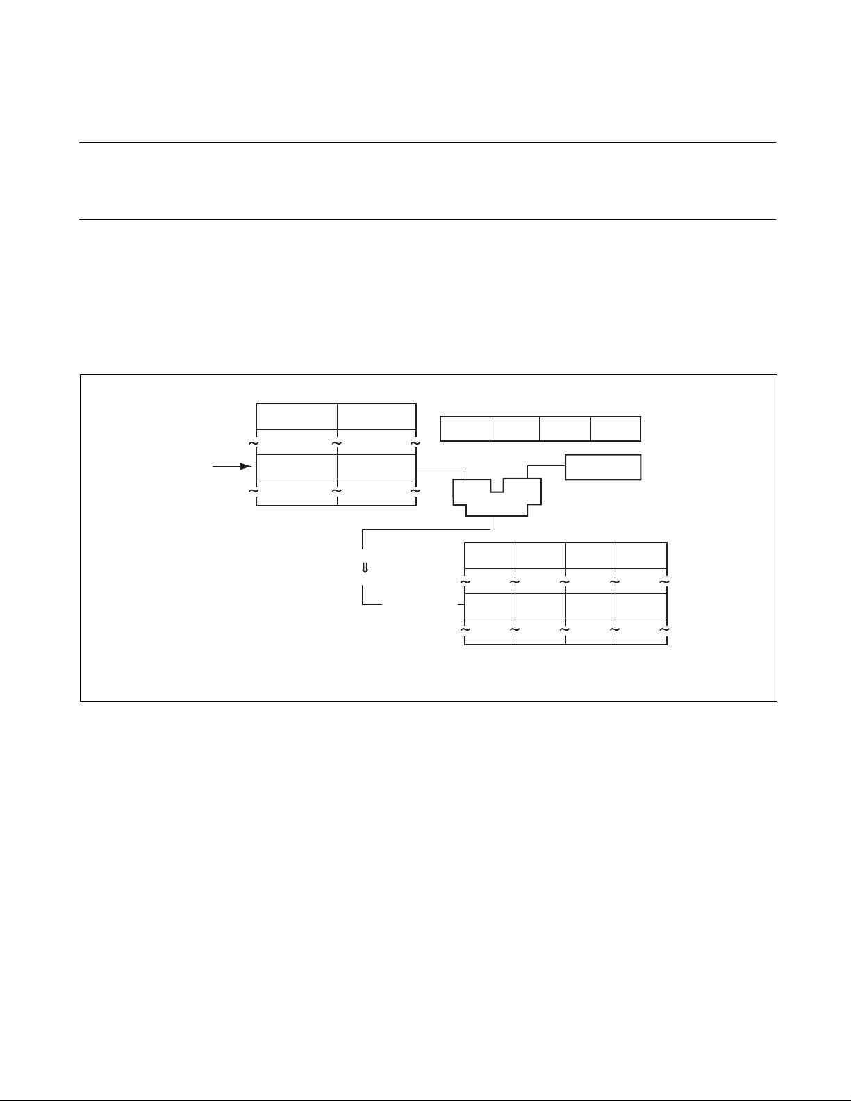
CHAPTER 3 REGISTER DESCRIPTIONS
3.3.3 Table Base Register (TBR)
The Table Base Register (TBR) designates the table containing the entry address for
"EIT" operations.
■ Overview of the Table Base Register
The Table Base Register (TBR) designates the table containing the entry address for "EIT" operations.
When an "EIT" condition occurs, the address of the vector reference is determined by the sum of the
contents of this register and the vector offset corresponding to the "EIT" operation.
Figure 3.3-7 shows an example of the operation of the table base register.
Figure 3.3-7 Sample of Table Base Register (TBR) Operation
Vector correspondence table
Vector no.
Vector offset
bit310
EAddr0 EAddr1 EAddr2 EAddr3
PC
Timer
interrupt
Note:
The process of referencing a vector table involves application of address alignment rules
11
H
3B8
H
H
+000003B8
876544DB
876544D8
Adder
H
H
H
+0 +1 +2 +387654123
EAddr0 EAddr1 EAddr2 EAddr3
87654123
Vector table
H
for word access.
TBR
23
Page 48

CHAPTER 3 REGISTER DESCRIPTIONS
■ Table Base Register Configuration
Figure 3.3-8 shows the bit configuration of the table base register.
Figure 3.3-8 Table Base Register Bit Configuration
Bit no.
TBR
31
■ Table Base Register Functions
● Vector Table Reference Addresses
Addresses for vector reference are generated by adding the contents of the "TBR" register and the vector
offset value, which is determined by the type of interrupt used. Because vector access is in word units, the
lower two bits of the resulting address value are explicitly read as "0".
● Vector Table Layout
Vector table layout can be realized in word (32 bits) units.
● Initial Values in Table Base Register
After a reset, the initial value is "000FFC00
".
H
■ Precautions Related to the Table Base Register
The "TBR" should not be assigned values greater than "FFFFFC00H". If values higher than this are placed
in the register, the operation may result in an overflow when summed wit h the offset value. An overflow
condition will result in vector access to the area "00000000
runaway.
00
" to "000003FFH", which can cause program
H
24
Page 49

CHAPTER 3 REGISTER DESCRIPTIONS
3.3.4 Return Pointer (RP)
The return pointer (RP) is a register used to contain the program counter (PC) value
during execution of call instructions, in order to assure return to the correct address
after the call instruction has executed.
■ Overview of the Return Pointer
The contents of the return pointer (RP) depend on the t ype of inst ruction. For a call instructio n with a del ay
slot, the value is the address stored +4, and for a call instruction with no delay slot, the value is the address
stored +2. The save data is returned from the "RP" pointer to the "PC" counter by execution of a "RET"
instruction.
Figure 3.3-9 shows a sample operation of the "RP" pointer in the execution of a "CALL" instruction with
no delay slot, and Figure 3.3-10 shows a sample operation of the "RP" pointer in the execution of a "RET"
instruction.
Figure 3.3-9 Sample Operation of "RP" in Execution of a "CALL" Instruction with No Delay Slot
Before execution
PC
12345678
RP
????????
Memory space
H
H
CALL SUB1
RET
After execution
PC
RP
SUB1
1234567A
H
Figure 3.3-10 Sample Operation of "RP" in Execution of a "RET" Instruction
Memory space
Before execution
PC
RP
SUB1
1234567A
CALL SUB1
ADD #1,R00 ADD #1,R00
H
SUB1 SUB1
RET
After execution
PC
1234567A
RP
1234567A
Memory space
CALL SUB1
SUB1SUB1
H
H
RET
Memory space
CALL:D SUB
RET
25
Page 50

CHAPTER 3 REGISTER DESCRIPTIONS
■ Return Pointer Configuration
Figure 3.3-11 shows the bit configurat i on of the return pointer.
Figure 3.3-11 Return Pointer Bit Configuration
Bit no.
RP
31
■ Return Pointer Functions
● Return Pointer in Multiple "CALL" Instructions
Because the "RP" does not have a stack configuration, it is necessary to first execute a save when calling
one subroutine from another subroutine.
● Initial Value of Return Pointer
The initial value is undefined.
00
26
Page 51

CHAPTER 3 REGISTER DESCRIPTIONS
3.3.5 System Stack Pointer (SSP), User Stack Pointer (USP)
The system stack pointer (SSP) and user stack pointer (USP) are registers that refe r to
the stack area. The "S" flag in the "CCR" determines whether the "SSP" or "USP" is
used. Also, when an "EIT" event occurs, the program counter (PC) and program status
(PS) values are saved to the stack area designated by the "SSP", regardless of the value
of the "S" flag at that time.
■ System Stack Pointer (SSP), User Stack Pointer (USP)
The system stack pointer (SSP) and user stack pointer (USP) are pointers that refer to the stack area. The
stack area is accessed by instructions that use general-purpose register "R15" as an indirect register, as well
as register multi-transfer instructions. "R15" is used as an indirect register by the "SSP" when the "S" flag
in the condition code register (CCR) is "0" and the "USP" when the "S" flag is "1". Also, when an "EIT"
event occurs, the program counter (PC) and program status (PS) values are saved to the stack area
designated by the "SSP", regardless of the value of the "S" flag at that time.
Figure 3.3-12 shows an example of stack pointer operation in executing the instruction "ST R13 , @-R15"
when the "S" flag is set to "0". Figure 3.3-13 shows an example of the same operation when the "S" flag is
set to "1".
Figure 3.3-12 Example of Stack Pointer Operation in Execution of Instruction "ST R13, @-R15"
when "S" Flag = 0
Before execution of ST R13,@-R15
Memory space
00000000
SSP
USP
R13
CCR
12345678
76543210H
17263540
SS
0
H
H
????????
????????
FFFFFFFF
H
H
After execution of ST R13,@-R15
Memory space
00000000H
SSP
USP
R13
CCR
12345674
76543210H
17263540
0
H
H
17263540H
????????
FFFFFFFF
H
27
Page 52

CHAPTER 3 REGISTER DESCRIPTIONS
Figure 3.3-13 Example of Stack Pointer Operation in Execution of Instruction "ST R13, @-R15"
when "S" Flag = 1
Before execution of ST R13,@-R15
Memory space
00000000
SSP
USP
R13
CCR
12345678
76543210H
17263540
SS
1
H
H
????????
????????
FFFFFFFF
■ Stack Pointer Configuration
Figure 3.3-14 shows the bit configuration of the stack pointer.
Figure 3.3-14 Bit Configuration of the Stack Pointers
Bit no.
SSP
31
After execution of ST R13,@-R15
Memory space
H
SSP
USP
R13
H
CCR
12345678
7654320CH
17263540
1
H
H
00000000H
17263540H
FFFFFFFF
H
00
USP
■ Functions of the System Stack Pointer and User Stack Pointer
● Automatic increment/decrement of stack pointer
The stack pointer uses automatic pre-decrement/post-increment counting.
● Stack Pointer Initial Value
The "SSP" has the initial value "00000000
". The "USP" initial value is undefined.
H
■ Recovery from EIT handler
When RETI instruction is used for recovery from an EIT handler, it is necessary to set the "S" flag to "0"
and select the system stack. For further details, see "
Operations in "EIT" Processing".
■ Recovery from EIT handler" of "4.2 Basic
28
Page 53

CHAPTER 3 REGISTER DESCRIPTIONS
3.3.6 Multiplication/Division Register (MD)
The multiplication/division register (MD) is a 64-bit register used to contain the result of
multiplication operations, as well as the dividend and result of division operations.
■ Overview of the Multiplication/Division Register
The multiplication/division register (MD) is a register used to contain the result of multiplication
operations, as well as the dividend and result of division operations. The products of multiplication are
stored in the "MD" in 64-bit format. In division operations, the dividend must first be placed in the lower
32 bits of the "MD" beforehand. Then as the division process is executed, the remainder is placed in the
higher 32 bits of the "MD", and the quotient in the lower 32 bits.
Figure 3.3-15 shows an example of the use of the "MD" in multiplication, and Figure 3.3-16 shows an
example of division.
Figure 3.3-15 Sample Operation of "MD" in Multiplication
Before execution of instruction MUL R00,R01
R00
R01
MD
12345678
76543210H
????????????????
H
H
Figure 3.3-16 Sample Operation of "MD" in Division
Before execution of stepwise division
R00
MD
12345678
????????76543210
H
Using R00
H
After execution of instruction MUL R00,R01
R00
12345678
R01
76543210H
MD
086A1C970B88D780
After execution of stepwise division
R00
12345678
MD
091A264000000006
H
H
H
H
29
Page 54

CHAPTER 3 REGISTER DESCRIPTIONS
■ Configuration of the "MD" Register
Figure 3.3-17 shows the bit configuration of the "MD".
Figure 3.3-17 Bit Configuration of the "MD"
Bit no.
MDH
MDL
31
■ Functions of the "MD"
Storing Results of Multiplication and Division
●
The results of multiplication operations are stored in the "MDH" (h igher 32 bits) and "MDL" (lower 32
bits) registers.
The results of division are stored as follows: quotients in the 32-bit "MDL" register, and remainders in the
32-bit "MDH" register.
● Initial Value of the "MD"
The initial value is undefined.
00
30
Page 55

CHAPTER 4
RESET AND "EIT"
PROCESSING
This chapter describes reset and "EIT" processing in the
FR family CPU.
A reset is a means of forcibly terminating the currently
executing process, initializing the entire device, and
restarting the program from the beginning. "EIT"
processing, in contrast, terminates the currently
executing process and saves restart information to the
memory, then transfers control to a predetermined
processing program. "EIT" processing programs can
return to the prior program by use of the "RETI"
instruction.
"EIT" processing operates in essentially the same
manner for exceptions, interrupts and traps, with the
following minor differences.
• Interrupts originate independently of the instruction
sequence. Processing is designed to resume from the
instruction immediately following the acceptance of
the interrupt.
• Exceptions are related to the instruction sequence,
and processing is designed to resume from the
instruction in which the exception occurred.
• Traps are also related to the instruction sequence,
and processing is designed to resume from the
instruction immediately following the instruction in
which the trap occurred.
31
Page 56

CHAPTER 4 RESET AND "EIT" PROCESSING
4.1 Reset Processing
4.2 Basic Operations in "EIT" Processing
4.3 Interrupts
4.4 Exception Processing
4.5 Traps
4.6 Priority Levels
32
Page 57

CHAPTER 4 RESET AND "EIT" PROCESSING
4.1 Reset Processing
A reset is a means of forcibly terminating the currently executing process, initializing
the entire device, and restarting the program from the beginning. Resets are used to
start the LSI operating from its initial state, as well as to recover from error conditions.
■ Reset Operations
When a reset is applied, the CPU terminates processing of the instruction executing at that time and goes
into inactive status until the reset is canceled. When the reset is canceled, the CPU i nitializes all internal
registers and starts execution beginning with the program indicated by the new value of the program
counter (PC).
■ Initialization of CPU Internal Register Values at Reset
When a reset is applied, the FR family CPU initializes internal registers to the following values.
• PC: Word data stored at address "000FFFFC
• ILM: "01111
• T Flag: "0" (trace OFF)
• I Flag: "0" (interrupt disabled)
• S Flag: "0" (use SSP pointer)
• TBR: "000FFC00
• SSP: "00000000
• R00 to R14: Undefined
• R15: SSP
For a description of built-in functions following a reset, refer to the Hardware Manual provided with each
FR family device.
■ Reset Priority Level
Resets have a higher priority than all "EIT" operations.
"
H
"
B
"
H
"
H
33
Page 58

CHAPTER 4 RESET AND "EIT" PROCESSING
4.2 Basic Operations in "EIT" Processing
Interrupts, exceptions and traps are similar operations applied under partially differing
conditions. Each "EIT" event involves terminating the execution of instructions, saving
information for restarting, and branching to a designated processing program.
■ Basic Operations in "EIT" Processing
The FR family device processes "EIT" events as follows.
(1) The vector table indicated by the table base register (TBR) and the number corresponding to the
particular "EIT" event are used to determine the entry address for the processing program for the
"EIT".
(2) For restarting purpo ses, the contents of the old program counter (PC) and the old program stat us (PS)
are saved to the stack area designated by the system stack pointer (SSP).
(3) After the pr ocessing flow is completed, the presence of new "EIT" sources is determined.
Figure 4.2-1 shows the operations in the "EIT" processing sequence.
Figure 4.2-1 "EIT" Processing Sequence
Instruction at which EIT event is detected
Canceled instruction
Canceled instruction
(1) Vector address calculation and new PC setting
EIT sequence
First instruction in EIT handler sequence (branching instruction)
(2) SSP update and PS save
(3) SSP update and PC save
(4) Detection of new EIT event
Note:
For a description of pipeline operations, see Section "5.1 Pipeline Operation".
IF ID EX MA WB
IF ID xxxx xxxx xxxx
IF xxxxxxxx xxxx xxxx
ID(1) EX(1) MA(1) WB(1)
ID(2) EX(2) MA(2) WB(2)
ID(3) EX(3) MA(3) WB(3)
ID(4) EX(4) MA(4) WB(4)
IF ID EX MA PC
34
Page 59
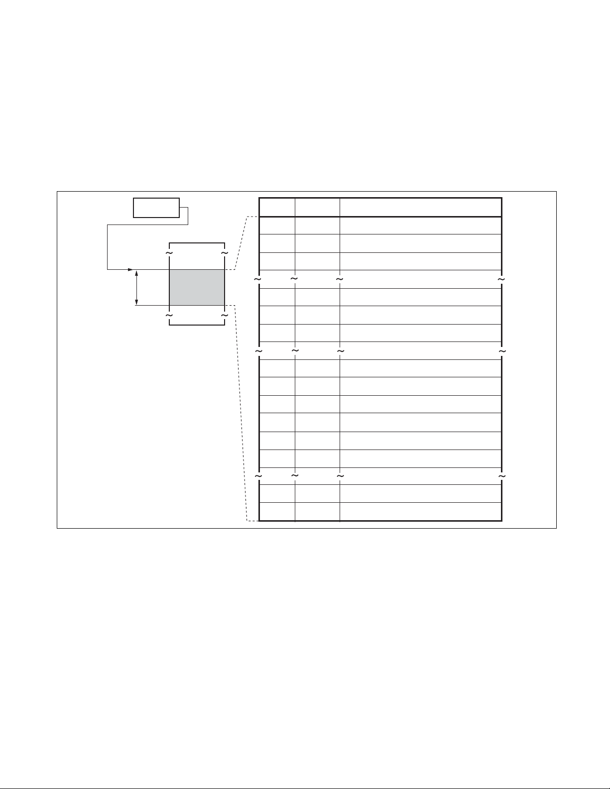
■ Vector Table Configuration
Vector tables are located in the main memory, occupying an area of 1 Kbyte beginning with the address
shown in the TBR. These areas are intended for use as a table of entry addresses for "EIT" processing,
however in applications where vector tables are not required, this area can be used as a normal instruction
or data area.
Figure 4.2-2 shows the structure of the vector table. (Example of 32-source)
Figure 4.2-2 Vector Table Configuration
CHAPTER 4 RESET AND "EIT" PROCESSING
TBR
00000000
1 Kbyte
FFFFFFFFH
Memory space
H
Offset Vector no. Description
000
H
004H
008H
33CH
340H
344H
3BCH
3C0H
3C4H
3C8H
3CCH
3D0H
3F8H
FFH
FEH
FDH
30H
2FH
2EH
10H
0FH
0EH
0DH
0CH
0BH
01H
INT #0FFH
INT #0FEH
INT #0FDH
INT #030H
INT #02FH or IR31
INT #02E
INT #010
INT #00F
Undefined instruction exception
Emulator exception
Step trace trap
Operand break trap
System reserved or Mode Vector
H or IR30
H or IR00
H or NMI
3FCH
00H
Reset
35
Page 60
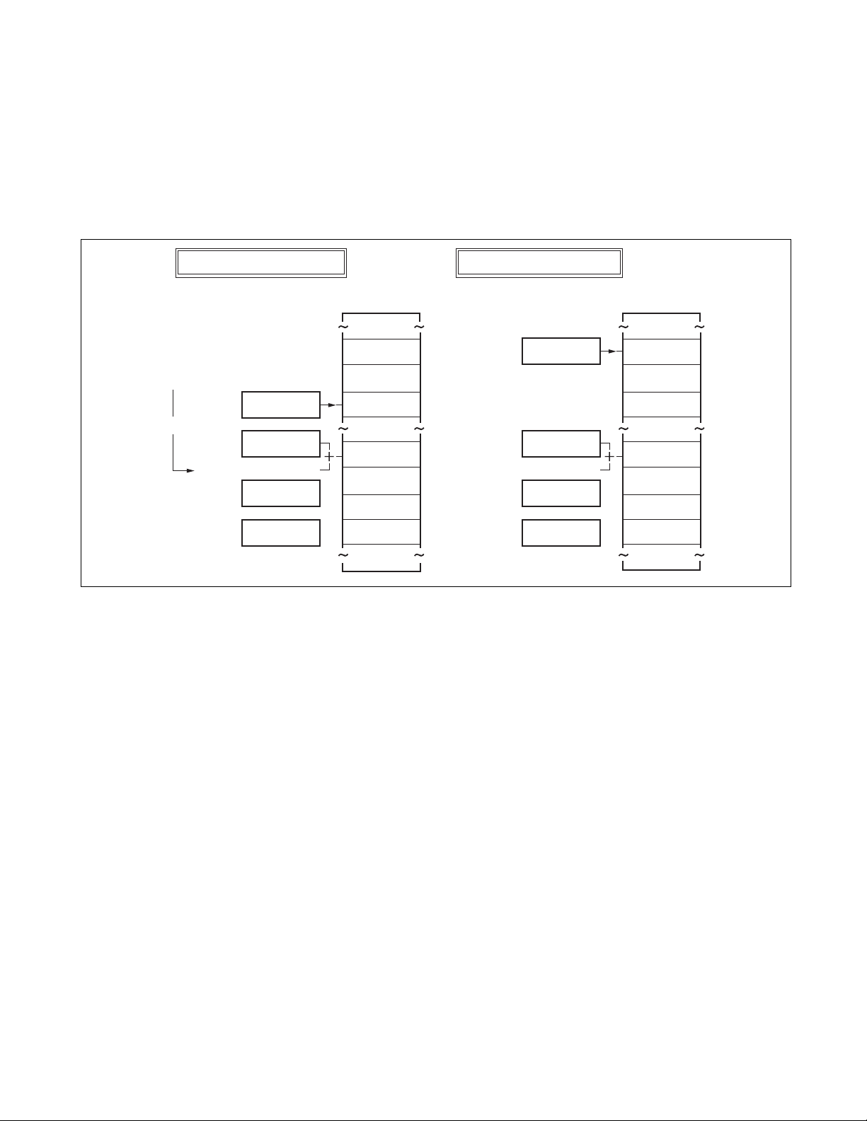
CHAPTER 4 RESET AND "EIT" PROCESSING
■ Saved Registers
Except in the case of reset processing, the values of the "PS" and "PC" are saved to the stack as designated
by the "SSP", regardless of the value of the "S" flag in the "CCR". No save operation is used in reset
processing.
Figure 4.2-3 illustrates the saving of the values of the "PC" and "PS" in "EIT" processing.
Figure 4.2-3 Saving "PC" and "PS" Values in "EIT" Processing
Immediately before interrupt
00000000H
7FFFFFF8H
Interrupt
SSP
IL=9
TBR
offset: 000003B8H
PC
PS
7FFFFFFCH
80000000
000FFC00H
12345678
000C0010H
FFFFFFFF
■ Recovery from EIT handler
RETI instruction is used for recovery from the EIT handler.
To insure the program execution results after recovery, it is required that all the contents of the CPU
register are saved.
Memory space
H
H
H
56781234
Immediately after interrupt
Memory space
00000000H
7FFFFFF8H
SSP
7FFFFFFCH
80000000H
TBR
PC
PS
000FFC00
56781234
00090010H
H
offset: 000003B8H
H
H
FFFFFFFF
12345678H
000C0010H
56781234H
H
36
Ensure that the PC and PS values in the stack are not overwritten unless necessary because those values,
saved in the stack at the occurrence of EIT, are recovered from the stack during the recovery sequence
using the RETI instruction. Be sure to set the "S" flag to "0" when the RETI instruction is executed.
Page 61

CHAPTER 4 RESET AND "EIT" PROCESSING
4.3 Interrupts
Interrupts originate independently of the instruction sequence. They are processed by
saving the necessary information to resume the currently executing instruction
sequence, and then starting the processing routine corresponding to the type of
interrupt that has occurred.
There are two types of interrupt sources.
• User interrupts
• Non-maskable interrupts (NMI)
■ Overview of Interrupt Processing
Interrupts originate independently of the instruction sequence. They are processed by saving the necessary
information to resume the currentl y executing instruction sequence, and then starting the processing routine
corresponding to the type of interrupt that has occurred.
Instructions loaded and executing in the CPU before the interrupt will be executed to completion, however,
any instructions loaded in the pipeline after the interrupt will be cancel ed. After completion of interrupt
processing, therefore, execution will return to the next instruction follow ing the generation of the i nterrupt
signal.
■ Sources of Interrupts
There are two types of interrupt sources.
• User interrupts (See Section "4.3.1 User Interrupts")
• Non-maskable interrupts (NMI) (See Section "4.3.2 Non-maskable Interrupts (NMI)")
■ Interrupts during Execution of Stepwise Division Programs
To enable resumption of processing when interrupts occur d uring stepwise division programs, in termediate
data is placed in the program status (PS), and saved to the stack. Therefore, if the interrupt processing
program overwrites the contents of the "PS" data in the stack, the processor will resume executing the
stepwise division instruction following the completion of interrup t processing, however the results of the
division calculation will be incorrect.
37
Page 62

CHAPTER 4 RESET AND "EIT" PROCESSING
4.3.1 User Interrupts
User interrupts originate as requests from peripheral circuits. Each interrupt request is
assigned an interrupt level, and it is possible to mask requests according to their level
values.
This section describes conditions for acceptance of user interrupts, as well as their
operation and uses.
■ Overview of User Interrupts
User interrupts originate as requests from peripheral circuits.
Each interrupt request is assigned an interrupt level, and it is possible to mask requests according to their
level values. Also, it is possible to disable all interrupts by using the I flag in the condition code register
(CCR) in the program status (PS).
It is possible to enter an interrupt signal through a signal pin, but in virtually all cases the interrupt
originates from the peripheral circuits contained on the FR family microcontrolle r chip itself.
■ Conditions for Acceptance of User Interrupt Requests
The CPU accepts user interrupts when the following conditions are met:
• The peripheral circuit is operating and generates an interrupt request.
• The interrupt enable bit in the peripheral circuit’s control register is set to "enable".
• The value of the interrupt request (ICR
• The "I" flag is set to "1".
*1: ICR = Interrupt Control Register ...a register on the microcontroller that contro ls inter ru pts
*2: ILM = Interrupt Level Mask Register ... a register in the CPU’s program status (PS)
*1
) is lower than the value of the ILM*2 setting.
■ Operation Following Acceptance of a User Interrupt
The following operating sequence takes place after a user interrupt is accepted.
• The contents of the program status (PS) are saved to the system stack.
• The address of the next instruction is saved to the system stack.
• The value of the system stack pointer (SSP) is reduced by 8.
• The value (level) of the accepted interrupt is stored in the "ILM".
• The value "0" is written to the "S" flag in the condition code register (CCR) in the program status (PS).
• The vector address of the accepted interrupt is stored in the program counter (PC).
38
Page 63

■ Time to Start of Interrupt Processing
The time required to start interrupt processing can be expressed as a maximum of "n + 6" cycles from the
start of the instruction currently executing when the interrupt was received, where "n" represents the
number of execution cycles in the instruction.
If the instruction includes memory access, or insufficient instructions are present, the corresponding
number of wait cycles must be added.
■ "PC" Values Saved for Interrupts
When an interrupt is accepted by the processor, those instructions in the pipeline that cannot be interrupted
in time will be executed. The remainder o f the inst ructions will be canceled, and will not be processed after
the interrupt. The "EIT" processing sequence saves "PC" values to the system stack representing the
addresses of canceled instructions.
■ How to Use User Interrupts
The following programming steps must be set up to enable the use of user interrupts.
Figure 4.3-1 illustrates the use of user interrupts.
CHAPTER 4 RESET AND "EIT" PROCESSING
Figure 4.3-1 How to Use User Interrupts
FR family CPU SSP USP
PS I ILM S
INT
OK
AND
Comparator
(2)
Interrupt
controller
(2)(6)(7)
ICR#n
Peripheral
device
Interrupt
enable bit
(5)(4)
Internal bus
(1) Enter values in the interrupt vector table (defined as data).
(2) Set up the "SSP" values.
(3) Set up the table base register (TBR) values.
(4) With in the interrupt controller, enter the appropriate level for the "ICR" corresponding to interrupts
from the peripheral from which the interrupt will originate.
(5) Initialize the peripheral function that requests the occurrence of the interrupt, and enable its interrupt
function.
(6) Set up the appropriate value in the "ILM" field in the "PS".
(7) Set the "I" flag to "1".
39
Page 64

CHAPTER 4 RESET AND "EIT" PROCESSING
4.3.2 Non-maskable Interrupts (NMI)
Non-maskable interrupts (NMI) are interrupts that cannot be masked. "NMI" requests
can be produced when "NMI" external signal pin input to the microcontroller is active.
This section describes conditions for the acceptance of "NMI" interrupts, as well as
their operation and uses.
■ Overview of Non-maskable Interrupts
Non-maskable interrupts (NMI) are interrupts that cannot be masked. "NMI" requests can be produced
when "NMI" external signal pin input to the microcontroller is active.
Non-maskable interrupts cannot be disabled by the "I" flag in the condition code register (CCR) in the
program status (PS).
The masking function of the interrupt level mask register (ILM) in th e "PS " is valid for "NMI ". However , it
is not possible to use the software input to set "ILM" values for masking of "NMI", so that these interru pts
cannot be masked by programming.
■ Conditions for Acceptance of Non-maskable Interrupt Requests
The FR family CPU will accept an "NMI" request when the following conditions are met:
● If "NMI" Pin Input is Active:
• In normal operation: Detection of a negative sign al edge
• In stop mode: Detection of an "L" level signal
● If the "ILM" V alue is Greater than 15.
■ Operation Following Acceptance of a Non-maskable Interrupt
When an "NMI" is accepted, the following operations take place:
(1) The contents of the "PS" are saved to the system stack.
(2) The address of the next instruction is saved to the system stack.
(3) The value of the system stack pointer (SSP) is reduced by 8.
(4) The value "15" is written to the "ILM".
(5) The value "0" is written to the "S" flag in "CCR" in the "PS".
(6) The value "TBR + 3C0
" is stored in the program counter (PC).
H
■ Time to Start of Non-maskable Interrupt Processing
The time required to start processing of an "NMI" can be expressed as a maximum of "n + 6" cycles from
the start of the instruction currently executing when the interrupt was received, where "n" represents the
number of execution cycles in the instruction.
If the instruction includes memory access, or insufficient instructions are present, the corresponding
number of wait cycles must be added.
40
Page 65

■ "PC" Values Saved for Non-maskable Interrupts
When an "NMI" is accepted by the processor, those instructions in the pipeline that cannot be interrupted in
time will be executed. The remainder of the instru ctions will be canceled, and will not be processed after
the interrupt. The "EIT" processing sequence saves "PC" values to the system stack representing the
addresses of canceled instructions.
■ How to Use Non-maskable Interrupts
The following programming steps must be set up to enable the use of "NMI".
(1) Enter values in the interrupt vector table (defined as data).
(2) Set up the "SSP" values.
(3) Set up "TBR" values.
(4) Set up the appropriate value in the "ILM" field in the "PS".
CHAPTER 4 RESET AND "EIT" PROCESSING
41
Page 66

CHAPTER 4 RESET AND "EIT" PROCESSING
4.4 Exception Processing
Exceptions originate from within the instruction sequence. Exceptions are processed
by first saving the necessary information to resume the currently executing instruction,
and then starting the processing routine corresponding to the type of exception that
has occurred.
■ Overview of Exception Processing
Exceptions originate from within the instruction sequence. Exceptions are processed by first saving the
necessary information to resume the currently executing instruction, and then starting the processing
routine corresponding to the type of exception that has occurred.
Branching to the exception processing routine takes place before execution of the instruction that has
caused the exception.
The address of the instruction in which the exception occurs becomes the program count er (PC) value that
is saved to the stack.
■ Factors Causing Exception Processing
The factor which causes the exception processing is the undefined-instruction exception (For details, see
"4.4.1 Undefined Instruction Exceptions").
42
Page 67

CHAPTER 4 RESET AND "EIT" PROCESSING
4.4.1 Undefined Instruction Exceptions
Undefined instruction exceptions are caused by attempts to execute instruction codes
that are not defined.
This section describes the operation, time requirements and uses of undefinedinstruction exceptions.
■ Overview of Undefined Instruction Exceptions
Undefined instruction exceptions are caused by attempts to execute instruction codes that are not defined.
■ Operations of Undefined Instruction Exceptions
The following operating sequence takes place when an undefined instruction exception occurs.
(1) The contents of the program status (PS) are saved to the system stack.
(2) The address of the instruction that caused the undefined-instruction exception is saved to the system
stack.
(3) The value of the system stack pointer (SSP) is reduced by 8.
(4) The value "0" is written to the "S" flag in the condition code register (CCR) in the "PS".
(5) The value "TBR + 3C4
" is stored in the program counter (PC).
H
■ Time to Start of Undefined Instruction Exception Processing
The time required to start exception processing is 7 cycles.
■ "PC" Values Saved for Undefined Instruction Exceptions
The address saved to the system stack as a "PC" value represents the instruction itself that caused the
undefined instruction exception. When a RETI instruction is executed, the contents of the system stack
should be rewritten with the exception processing routine so that execution will either resume from the
address of the next instruction after the instruction that caused the exception, or branch to the appropriate
processing routine.
■ How to Use Undefined Instruction Exceptions
The following programming steps must be set up to enable the use of undefined instruction exceptions.
(1) Enter values in the interrupt vector table (defined as data).
(2) Set up the "SSP" value.
(3) Set up "TBR" value.
■ Undefined Instructions Placed in Delay Slots
Undefined instructions placed in delay slots do not generate undefined instruction exceptions. In such
cases, undefined instructions have the same operation as "NOP" instructions.
43
Page 68

CHAPTER 4 RESET AND "EIT" PROCESSING
4.5 Traps
Traps originate from within the instruction sequence. Traps are processed by first
saving the necessary information to resume processing from the next instruction in the
sequence, and then starting the processing routine corresponding to the type of trap
that has occurred.
Sources of traps include the following:
• "INT" instructions
• "INTE" instructions
• Step trace traps
• Coprocessor not found traps
• Coprocessor error traps
■ Overview of Traps
Traps originate from within the instruction sequence. Traps are processed by first saving the necessary
information to resume processing from the next instruction in the sequence, and then starting the processing
routine corresponding to the type of trap that has occurred.
Branching to the exception processing routine takes place after execution of the instruction that has caused
the exception.
The address of the instruction in which the exception occurs becomes the program count er (PC) value that
is saved to the stack.
■ Sources of Traps
Sources of traps include the following:
• INT instructions (For details, see Section "4.5.1 "INT" Instructions")
• INTE instructions (For details, see Section "4.5.2 "INTE" Instruction")
• Step trace traps (For details, see Section "4.5.3 Step Trace Traps")
• Coprocessor not found traps (For details, see Section "4.5.4 Coprocessor Not Found Traps")
• Coprocessor error traps (For details, see Section "4.5.5 Coprocessor Error Trap")
44
Page 69

CHAPTER 4 RESET AND "EIT" PROCESSING
4.5.1 "INT" Instructions
The "INT" instruction is used to create a software trap.
This section describes the operation, time requirements, program counter (PC) values
saved, and other information of the "INT" instruction.
■ Overview of the "INT" Instruction
The "INT #u8" instruction is used to create a software trap with the interrupt number designated in the
operand.
■ "INT" Instruction Operation
When the "INT #u8" instruction is executed, the following operations take place.
(1) The contents of the program status (PS) are saved to the system stack.
(2) The address of the next instruction is saved to the system stack.
(3) The value of the system stack pointer (SSP) is reduced by 8.
(4) The value "0" is written to the "I" flag in the condition code register (CCR) in the "PS".
(5) The value "0" is written to the "S" flag in the "CCR" in the "PS".
(6) The value "TBR + 3FC
– 4 × u8" is stored in "PC".
H
■ Time to Start of Trap Processing for "INT" Instructions
The time required to start trap processing is 6 cycles.
■ "PC" Values Saved for "INT" Instruction Execution
The "PC" value saved to the system stack represents the address of the next instruction after the "INT"
instruction.
■ Precautionary Information for Use of "INT" Instructions
The "INT" instruction should not be used within an "INTE" instruction handler or step trace trap-handler
routine. This will prevent normal operation from resuming after the "RETI" instruction.
45
Page 70

CHAPTER 4 RESET AND "EIT" PROCESSING
4.5.2 "INTE" Instruction
The "INTE" instruction is used to create a software trap for debugging.
This section describes the operation, time requirements, program counter (PC) values
saved, and other information of the "INTE" instruction.
■ Overview of the "INTE" Instruction
The "INTE" instruction is used to create a software trap for debugging. This instruction allows the u se of
emulators.
This technique can be utilized by users for systems that have not been debugged by emulators.
■ "INTE" Instruction Operation
When the "INTE" instruction is executed, the following operations take place.
(1) The contents of the program status (PS) are saved to the system stack.
(2) The address of the next instruction is saved to the system stack.
(3) The value of the system stack pointer (SSP) is reduced by 8.
(4) The value "4" is written to the interrupt level mask register (ILM) in the "PS".
(5) The value "0" is written to the "S" flag in the "CCR" in the "PS".
(6) The value "TBR + 3D8
" is stored in "PC".
H
■ Time to Start of Trap Processing for "INTE" Instructions
The time required to start trap processing is 6 cycles.
■ "PC" Values Saved for "INTE" Instruction Execution
The "PC" value saved to the system stack represents the address of the next instruction after the "INTE"
instruction.
■ Precautionary Information for Use of "INTE" Instructions
The "INTE" instruction cannot be used in user programs involving debu gging with an emulator. Also, the
"INTE" instruction should not be used within an "INTE" instruction handler or step trace trap-handler
routine. This will prevent normal operation from resuming after the "RETI" instruct ion. Note also that no
"EIT" events can be generated by "INTE" instructions during stepwise execution.
46
Page 71

CHAPTER 4 RESET AND "EIT" PROCESSING
4.5.3 Step Trace Traps
Step trace traps are traps used by debuggers. This type of trap can be created for each
individual instruction in a sequence by setting the "T" flag in the system condition code
register (SCR) in the program status (PS).
This section describes conditions for the generation, operations, program counter (PC)
values saved, and other information of step trace traps.
■ Overview of Step Trace Traps
Step trace traps are traps used by debuggers. This type of trap can be created for each individual instruction
in a sequence, by setting the "T" flag in the "SCR" in the "PS".
In the execution of delayed branching instructions, step trace traps are not generated immediately after the
execution of branching. The trap is generated after execution of the instruction(s) in the delay slot.
The step trace trap can be utilized by users for systems that have not been debugged by emulators.
■ Conditions for Generation of Step Trace Traps
A step trace trap is generated when the following conditions are met.
• The "T" flag in the "SCR" in the "PS" is set to "1".
• The currently executing instruction is not a delayed branching instruction.
• The CPU is not processing an "INTE" instruction or a step trace trap processing routine.
■ Step Trace Trap Operation
When a step trace trap is generated, the following operations take place.
(1) The contents of the program status (PS) are saved to the system stack.
(2) The address of the next instruction is saved to the system stack.
(3) The value of the system stack pointer (SSP) is reduced by 8.
(4) The value "0" is written to the "S" flag in the "CCR" in the "PS".
(5) The value "TBR + 3C4
" is stored in "PC".
H
■ "PC" Values Saved for Step Trace Traps
The "PC" value saved to the system stack represents the address of the next instruction after the step trace
trap.
■ Relation of Step Trace Traps to "NMI" and External Interrupts
When the "T" flag is set to enable step trace traps, both "NMI" and external interrupts are disabled.
■ Precautionary Information for Use of Step Trace Traps
Step trace traps cannot be used in user programs involving debugging with an emulator. No te also that no
"EIT" events can be generated by "INTE" instructions when the step trace trap function is used.
47
Page 72

CHAPTER 4 RESET AND "EIT" PROCESSING
4.5.4 Coprocessor Not Found Traps
Coprocessor not found traps are generated by executing coprocessor instructions
using coprocessors not found in the system.
This section describes conditions for the generation of coprocessor not found traps, in
addition to operation, program counter (PC) values saved, and other information.
■ Overview of Coprocessor Not Found Traps
Coprocessor not found traps are generated by executing coprocessor instructions using coprocessors not
found in the system.
■ Conditions for Generation of Coprocessor Not Found Traps
A coprocessor not found trap is generated when the following conditions are met.
• Execution of a "COPOP/COPLD/COPST/COPSV" instruction.
• No coprocessor present in the system corresponds to the operand "#u4" in any of the above instructions.
■ Coprocessor Not Found Trap Operation
When a coprocessor not found trap is generated, the following operations take place.
(1) The contents of the program status (PS) are saved to the system stack.
(2) The address of the next instruction is saved to the system stack.
(3) The value of the system stack pointer (SSP) is reduced by 8.
(4) The value "0" is written to the "S" flag in the condition code register (CCR) in the "PS".
(5) The value "TBR + 3E0
" is stored in "PC".
H
■ "PC" Values Saved for Coprocessor Not Present Traps
The "PC" value saved to the system stack represents the address of the next instruction after the
coprocessor instruction that caused the trap.
■ General-purpose Registers during Execution of "COPST/COPSV" Instructions
Execution of any "COPST/COPSV" instruction referring to a coprocessor that is not present in the system
will cause undefined values to be transferred to the general-purpose register (R0 to R14) designated i n the
operand. The coprocessor not found trap will be activated after the designated general-purpose register is
updated.
48
Page 73

CHAPTER 4 RESET AND "EIT" PROCESSING
4.5.5 Coprocessor Error Trap
A coprocessor error trap is generated when an error has occurred in a coprocessor
operation and the CPU executes another coprocessor instruction involving the same
coprocessor.
This section describes conditions for the generation, operations, and program counter
(PC) values saved of coprocessor error traps.
■ Overview of Coprocessor Error Traps
A coprocessor error trap is generated when an error has occurred in a coprocessor operation and the CPU
executes another coprocessor instruction involvin g the same coprocessor. Note that no coprocessor error
traps are generated for execution of "COPSV" instructions.
■ Conditions for Generation of Coprocessor Erro r Traps
A coprocessor error trap is generated when the following conditions are met.
• An error has occurred in coprocessor operation.
• A "COPOP/COPLD/COPST" instruction is executed involving th e same coprocessor.
■ Coprocessor Error Trap Operation
When a coprocessor error trap is generated, the following operations take place.
(1) The contents of the program status (PS) are saved to the system stack.
(2) The address of the next instruction is saved to the system stack.
(3) The value of the system stack pointer (SSP) is reduced by 8.
(4) The value "0" is written to the "S" flag in the condition code register (CCR) in the "PS".
(5) The value "TBR + 3DC
" is stored in "PC".
H
■ "PC" Values Saved for Coprocessor Error Traps
The "PC" value saved to the system stack represents the address of the next instruction after the
coprocessor instruction that caused the trap.
■ Results of Coprocessor Operations after a Coprocessor Error Trap
Despite the occurrence of a coprocessor error trap, the execution of the coprocessor instruction ("COPOP/
COPLD/COPST") remains valid and the results of the instruction are retained. Note that the results of
operations affected by the coprocessor error will not be correct.
49
Page 74

CHAPTER 4 RESET AND "EIT" PROCESSING
■ Saving and Restoring Coprocessor Error Information
When a coprocessor is used in a multi-tasking environment, the internal resources of the coprocessor
become part of the system context. Thus whenever context switching occurs, it is necessary to save or
restore the contents of the coprocessor. Problems arise when there are hidden coprocessor errors remaining
from former tasks at the time of context switching.
In such cases, when the exception is detected in a coprocessor context save instruction by the dispatcher, it
becomes impossible to return the information to the former task. This problem is avoided by executing a
"COPSV" instruction, which does not send notification of coprocessor errors but acts to clear the internal
error. Note that the error information is retained in the status information that is saved. If the saved status
information is returned to the coprocessor at the time of re-dispatching to the former task , the hidden error
condition is cleared and the CPU is notified when the next coprocessor instruction is executed.
Figure 4.5-1 shows an example in which notification to the coprocessor does not succeed, and Figure 4.5-2
illustrates the use of the "COPSV" instruction to save and restore error information.
Figure 4.5-1 Example: Coprocessor Error Notification Not Successful
Coprocessor
CPU(main)
COPOP
Interrupt
CPU(dispatcher)
Hidden error condition
Notification
COPST
Figure 4.5-2 Use of "COPSV" Instruction to Save and Restore Error Information
Coprocessor
CPU
(main)
CPU(dispatcher)
COPOP
Interrupt
Hidden error condition Hidden error condition
No notification
COPST
RETI
50
COPSV COPLD
Page 75

CHAPTER 4 RESET AND "EIT" PROCESSING
4.6 Priority Levels
When multiple "EIT" requests occur at the same time, priority levels are used to select
one source and execute the corresponding "EIT" sequence. After the "EIT" sequence is
completed, "EIT" request detection is applied again to enable processing of multiple
"EIT" requests.
Acceptance of certain types of "EIT" requests can mask other factors. In such cases the
priority applied by the "EIT" processing handler may not match the priority of the
requests.
■ Priority of Simultaneous Occurrences
The FR family uses a hardware function to determine the priority of acceptance of "EIT" requests.
Table 4.6-1 shows the priority levels of "EIT" requests.
Table 4.6-1 Priority of "EIT" Requests
Priority Source Masking of other sources
1 Reset Other sources discarded
2 Undefined instruction exception Other sources disabled
INT instruction I flag = 0
3
4 User interrupt ILM = level of source accepted
5 NMI ILM = 15
6 Step trace trap ILM = 4
7 INTE instruction ILM = 4
Coprocessor not found trap
Coprocessor error trap
None
51
Page 76

CHAPTER 4 RESET AND "EIT" PROCESSING
■ Priority of Multiple Processes
When the acceptance of an "EIT" source results in the masking of other sources, the priority of execution of
simultaneously occurring "EIT" handlers is as shown in Table 4.6-2.
Table 4.6-2 Priority of Execution of "EIT" Handler s
Priority Source Masking of other sources
1 Reset Other sources discarded
2 Undefined instruction exception Other sources disabled
3 Step trace trap ILM = 4 *
4 INTE instruction ILM = 4 *
5 NMI ILM = 15
6 INT instruction I flag = 0
7 User interrupt ILM = level of source accepted
8
*: When "INTE" instructions are run stepwise, only the step trace "EIT" is generated.
Sources related to the "INTE" instruction will be ignored.
Coprocessor not found trap
Coprocessor error trap
None
52
Page 77

CHAPTER 5
PRECAUTIONARY
INFORMATION FOR THE FR
FAMILY CPU
This chapter presents precautionary information related
to the use of the FR family CPU.
5.1 Pipeline Operation
5.2 Pipeline Operation and Interrupt Processing
5.3 Register Hazards
5.4 Delayed Branching Processing
53
Page 78

CHAPTER 5 PRECAUTIONARY INFORMATION FOR THE FR FAMILY CPU
5.1 Pipeline Operation
The FR family CPU processes all instructions using a 5-stage pipeline operation. This
makes it possible to process nearly all instructions within one cyc l e.
■ Overview of Pipeline Operation
In a pipeline operation the steps by which the CPU interprets and executes instructions are divided into
several cycles, so that instructions can be processed simultaneously in successive cycles. This enables the
system to appear to execute in one cycle many instructions that would require several cycles in other
methods of processing. The FR family CPU simultaneously executes five types (IF, ID, EX, MA, and WB)
of processing cycles, as shown in Figure 5.1-1. This is referred to as five-stage pipeline processing.
• IF: Load instruction
• ID: Int e rpr e t instr uction
• EX: Execute instruction
• MA: Memory access
• WB: Write to register
Figure 5.1-1 Example of Pipeline Operation in the FR Family CPU
(1) (2) (3) (4) (5)
LD @R10, R1
LD @R11, R2
ADD R1, R3
BNE:D TestOK
ST R2, @R12
IF ID EX MA WB
IF ID EX MA WB
IF ID EX MA WB
IF ID EX MA WB
IF ID EX MA WB
● Processes occurring in each 1 cycle in the above example:
(1) Load instructi on "LD @R10,R1"
(2) Interpret instruction "LD @R10,R1" Load instruction "LD, @R11,R2"
(3) Execute instruction "LD @R10,R1" Interpret instruction "LD, @R11,R2"
Load instruction, "ADD R1, R3"
(4) Memory access instruction "LD @R10,R1" Execute instruction "LD, @R11,R2"
Interpret instruction, "ADD R1, R3" Load instruction "BNE:D TestOK"
(5) Write instruction "LD @R10,R1" to register Memory access instruction "LD, @R11,R2"
Execute instruction, "ADD R1, R3" Interpret instruction, "BNE:D TestOK"
Load instruction "ST R2,@R12"
1 cycle
54
Page 79

CHAPTER 5 PRECAUTIONARY INFORMATION FOR THE FR FAMILY CPU
5.2 Pipeline Operation and Interrupt Processing
The FR family CPU processes all instructions through pipeline operation. Therefore,
particularly for instructions that start hardware events, it is possible for contradictory
conditions to exist before and after an instruction.
■ Precautionary Information for Interrupt Processing in Pipeline Operation
Because the FR family CPU operates in pipeline mode, the recognition of an interrupt signal is preceded by
several instructions in respective states of pipeline processing. If one of those instructions bein g executed in
the pipeline acts to delete the interrupt, the CPU will branch normally to the respective interrupt processing
program but when control is transferred to interrupt processing the interrupt request will no longer be
effective.
Note that this type of condition does not occur in exception or trap processing.
Figure 5.2-1 Example: Interrupt Accepted and Deleted Causing Mismatched Pipeline Conditions
Interrupt request
None None None None None None None
Generated Deleted
LD @R10, R1
ST R2, @R11
ADD R1, R3(cancelled)
BNE TestOK(cancelled)
EIT sequence execution #1
--: Canceled stages
IF ID EX MA WB
IF ID EX MA WB
IF ID --
IF
■ Conditions that Are Actually Generated
The following processing conditions may cause an interrupt to be deleted after acceptance.
• A program that clears interrupt sources while in interrupt-enabled mode
• Writing to an interrupt-enable bit in a peripheral function while in interrupt-enabled mode
■ How to Avoid Mismatched Pipeline Conditions
To avoid deleting interrupts that have already been accepted, programmers should use the "I" flag in the
condition code register (CCR) in the program status (PS) to regulate interrupt sources.
-- --
-- -- -- --
IF ID EX MA WB
55
Page 80

CHAPTER 5 PRECAUTIONARY INFORMATION FOR THE FR FAMILY CPU
5.3 Register Hazards
The FR family CPU executes program steps in the order in which they are written, and is
therefore equipped with a function that detects the occurrence of register hazards and
stops pipeline processing when necessary. This enables programs to be written without
attention to the order in which registers are used
■ Overview of Register Hazards
The CPU in pipeline operation may simultaneously process o ne inst ruction that invo lves w riting values to a
register, and a subsequent instruction that attempts to refer to the same register before the write process is
completed. This is called a register hazard.
In the example in Figure 5.3-1, the program will read the address value at "R1" before the desired value has
been written to "R1" by the previous instruction. As a result, the old value at "R1" will be read instead of
the new value.
Figure 5.3-1 Example of a Register Hazard
ADD R0, R1
■ Register Bypassing
Even when a register hazard does occur, it is possible to process instructions without operating delays if the
data intended for the register to be accessed can be extricated from the preceding instruction. This type of
data transfer processing is called register bypassing, and the FR family CPU is equipped with a register
bypass function.
In the example in Figure 5.3-2, instead of reading the "R1" in the "ID" stage of the "SUB" instruction, the
program uses the results of the calculation from the "EX" stage of the "ADD" instruction (before the results
are written to the register) and thus executes the instruction without delay.
ADD R0, R1
IF ID EX MA WB : Write cycle to R1
IF ID EX MA WBSUB R1, R2
Figure 5.3-2 Example of a Register By pass
IF ID EX MA WB : Data calculation cycle to R1
IF ID EX MA WBSUB R1, R2
: Read cycle from R1
: Read cycle from R1
56
Page 81

■ Interlocking
Instructions which are relatively slow in loading data to the CPU may cause register hazards that cannot be
handled by register bypassing.
In the example in Figure 5.3-3, data required for the "ID" stage of the "SUB" instruction must be loaded to
the CPU in the "MA" stage of the "LD" instruction, creating a hazard that cannot be avoided by the bypass
function.
Figure 5.3-3 Example: Register Hazard that Cannot be Avoided by Bypassing
CHAPTER 5 PRECAUTIONARY INFORMATION FOR THE FR FAMILY CPU
LD @R0, R1
IF ID EX MA WB : Data read cycle to R0
IF ID EX MA WBSUB R1, R2
: Read cycle from R1
In cases such as this, the FR family CPU executes the instruction correctly by pausing before execu tion of
the subsequent instruction. This function is called interlocking.
In the example in Figure 5.3-4, the "ID" stage of the "SUB" instruction is delayed until the data is loaded
from the "MA" stage of the "LD" instruction.
Figure 5.3-4 Example of Interlocking
LD @R0, R1
IF ID EX MA WB : Data read cycle to R0
IF ID ID MAEX WBSUB R1, R2
: Read cycle from R1
■ Interlocking Produced by Reference to "R15" and General-purpose Registers after
Changing the "S" Flag
The general-purpose register "R15" is designed to function as either the system stack pointer (SSP) or user
stack pointer (USP). For this reason, the FR fam ily CPU is designed to au tomatically generate an interlock
whenever a change to the "S" flag in the condition code register (CCR) in the program status (PS) is
followed immediately by an instruction that references the "R15". This interlock enables the CPU to
reference the "SSP" or "USP" values in the order in which they are written in the program. FR family
hardware design similarly generates an interlock whenever a TYPE-A format instruction immediately
follows an instruction that changes the value of the "S" flag.
For information on instruction format types, see Section "6.1 Instruction Formats".
57
Page 82

CHAPTER 5 PRECAUTIONARY INFORMATION FOR THE FR FAMILY CPU
5.4 Delayed Branching Processing
Because the FR family CPU features pipeline operation, branching instructions must
first be loaded before they are executed. Delayed branching processing is the function
to execute the loaded instruction, and allows to accelerate processing speeds.
■ Overview of Branching with Non-delayed Branching Instructions
In a pipeline operation, by the time the CPU recogni zes an instruction as a branching instruction the next
instruction has already been loaded. To process the program as written, the instruction following the
branching instruction must be canceled in the middle of execution. Branching instructions that are handled
in this manner are non-delayed branching instructions.
Examples of processing non-delayed branching instructions (both when branching conditions are satisfied
and not satisfied) are described in Section "5.4.1 Processing Non-delayed Branching Instructions".
■ Overview of Branching with Delayed Branching Instructions
An instruction immediately following a branching instru ction will already be loaded by the CPU by the
time the branching instruction is executed. This position is called the delay slot.
A delayed branching instruction is a branching instruction that executes the instru ction in the delay slot
regardless of whether the branching conditions are satisfied or not satisfied.
Examples of processing delayed branching instructions (both when branching conditions are satisfied and
not satisfied) are described in Section "5.4.2 Processing Delayed Branching Instructions".
■ Instructions Prohibited in Delay Slots
The following instructions may not be used in delayed branching processing by the FR family CPU.
• LDI:32 #i32, Ri LDI:20 #i20, Ri
• COPOP #u4, #CC, CRj, CRi
COPLD #u4, #CC, Rj, CRi
COPST #u4, #CC, CRj, Ri
COPSV #u4, #CC, CRj, Ri
• JMP @Ri
CALL label12
CALL @Ri
RET
Conditional branching instruction and related delayed branching instructions
• INT #u8
RETI
INTE
58
Page 83

CHAPTER 5 PRECAUTIONARY INFORMATION FOR THE FR FAMILY CPU
•AND Rj, @Ri
ANDH Rj, @Ri
ANDB Rj, @Ri
OR Rj, @Ri
ORH Rj, @Ri
ORB Rj, @Ri
EOR Rj, @Ri
EORH Rj, @Ri
EORB Rj, @Ri
• BANDH #u4, @R i
BANDL #u4, @Ri
BORH #u4, @Ri
BORL #u4, @R i
BEORH #u4, @Ri
BEORL #u4, @Ri
BTSTH #u4, @Ri
BTSTL #u4, @Ri
• MUL Rj, Ri
MULU Rj, Ri
MULH Rj, Ri
MULUH Rj, Ri
•LD @R15+, PS
• LDM0 (reglist)
LDM1 (reglist)
STM0 (reglist)
STM1 (reglist)
ENTER #u10
XCHB @Rj, Ri
• DMOV @dir10, @R13+
DMOV @R13+, @dir10
DMOV @dir10, @-R15
DMOV @R15+, @dir10
DMOVH @dir9, @R13+
DMOVH @R13+, @dir9
DMOVB @dir8, @R13+
DMOVB @R13+, @dir8
■ Restrictions on Interrupts during Processing of Delayed Branching Instructions
"EIT" processing is not accepted during execution of delayed branching instructions or delayed branching
processing.
59
Page 84

CHAPTER 5 PRECAUTIONARY INFORMATION FOR THE FR FAMILY CPU
5.4.1 Processing Non-delayed Branching Instructions
The FR family CPU processes non-dela yed branc hing instructions in the or der in whic h the
program is written, introducing a 1-cyc le dela y in e x ecution speed if branc hing takes place.
■ Examples of Processing Non-delayed Branching Instructions
Figure 5.4-1 shows an example of processing a non-delayed branching instruction when branching
conditions are satisfied.
In this example, the instruction "ST R2,@R12" (which immediately follows the branching instru ction) has
entered the pipeline operation before the fetching of the branch destination instruction, but is canceled
during execution.
As a result, the program is processed in the order in which it is written, and the branching instruction
requires an apparent processing time of two cycles.
Figure 5.4-1 Example: Processing a Non-delayed Branching Instruction (Branching Conditions Satisfied)
LD @R10, R1
LD @R11, R2
ADD R1, R3
BNE TestOK(branching conditions satisfied)
ST R2, @R12(instruction immediately after)
ST R2, @R13(branch destination instruction)
-- : Canceled stages
: PC change
IF ID EX MA WB
IF ID EX MA WB
IF ID EX MA WB
IF ID EX MA WB
IF -- -- -- --
IF ID EX MA WB
Figure 5.4-2 shows an example of processing a non-delayed branching instruction when branching
conditions are not satisfied.
In this example, the instruction "ST R2,@R12" (which immediately follows the branching instru ction) has
entered the pipeline operation before the fetching of the branch destination instruction, and is executed
without being canceled.
Because instructions are executed without branching, the program is processed in the order in which it is
written. The branching instruction requires an apparent processing time of one cycle.
Figure 5.4-2 Example: Processing a Non-delayed Branching Instruction (Branching Conditions Not Satisfied)
60
LD @R10, R1
LD @R11, R2
ADD R1, R3
BNE TestOK(branching conditions not satisfied)
ST R2, @R12(instruction immediately after)
ADD #4, R12(subsequent instruction)
IF ID EX MA WB
IF ID EX MA WB
IF ID EX MA WB
IF ID EX MA WB
IF ID EX MA WB
IF ID EX MA WB
Not canceled
Page 85

CHAPTER 5 PRECAUTIONARY INFORMATION FOR THE FR FAMILY CPU
5.4.2 Processing Delayed Branching Instructions
The FR family CPU processes delayed branching instructions with an apparent
execution speed of 1 cycle, regardless of whether branching conditions are satisfied or
not satisfied. When branching occurs, this is one cycle faster than using
non-delayed branching instructions.
However, the apparent order of instruction processing is inverted in cases where
branching occurs.
■ Examples of Processing Delayed Branching Instructions
Figure 5.4-3 shows an example of processing a delayed branching instruction when branching conditions
are satisfied.
In this example, the branch destination instruction, "ST R2,@R13" is executed after the instruction "ST
R2,@R12" in the delay slot. As a result, the branching instruction has an apparent execution speed of one
cycle. However, the instruction "ST R2,@R12" in the delay slot is executed before the branch destination
instruction "ST R2,@R13" and therefore the apparent order of processing is inverted.
Figure 5.4-3 Example: Processing a Delayed Branching Instruction (Branching Condition Satisfied)
LD @R10, R1
LD @R11, R2
ADD R1, R3
BNE:D TestOK(branching conditions satisfied)
ST R2, @R12(delay slot instruction)
ST R2, @R13(branch destination instruction)
: PC change
IF ID EX MA WB
IF ID EX MA WB
IF ID EX MA WB
IF ID EX MA WB
IF ID EX MA WB
Not canceled
IF ID EX MA WB
Figure 5.4-4 shows an example of processing a delayed branching instruction when branching conditions
are not satisfied.
In this example the delay slot instruction "ST R2,@R12" is executed without being canceled. As a result,
the program is processed in the order in which it is written. The branching instructi on requires an apparent
processing time of one cycle.
Figure 5.4-4 Example: Processing a Delayed Branching Instruction (Branching Conditions Not Satisfied)
LD @R10, R1
LD @R11, R2
IF ID EX MA WB
IF ID EX MA WB
ADD R1, R3
BNE:D TestOK (branching conditions not satisfied)
ST R2, @R12 (delay slot instruction)
ADD #4, R12
IF ID EX MA WB
IF ID EX MA WB
IF ID EX MA WB
IF ID EX MA WB
Not canceled
61
Page 86

CHAPTER 5 PRECAUTIONARY INFORMATION FOR THE FR FAMILY CPU
■ Examples of Programing Delayed Branching Instructions
An example of programing a delayed branching instruction is shown below.
.
.
LD @R10, R1
LD @R11, R2
ADD R1, R3
BNE:D TestOK
ST R2, @R12
ADD #4, R12 ; not satisfy
.
.
.
TestOK: ; satisfied
ST R2, @R13
.
.
62
Page 87

CHAPTER 6
INSTRUCTION OVERVIEW
This chapter presents an overview of the instructions
used with the FR family CPU.
All FR family CPU instructions are in 16-bit fixed length
format, except fo r immediate data transfer instructions
which may exceed 16 bits in length. This f o rmat enables
the creation of a compact object code and smoother
pipeline processing.
6.1 Instruction Formats
6.2 Instruction Notation Formats
63
Page 88

CHAPTER 6 INSTRUCTION OVERVIEW
6.1 Instruction Formats
The FR family CPU uses six types of instruction format, TYPE-A through TYPE-F.
■ Instruction Formats
All instructions used by the FR family CPU are written in the six formats shown in Figur e 6.1-1.
Figure 6.1-1 Instruction Formats
TYPE-A
TYPE-B
TYPE-C
TYPE-D
TYPE-E
TYPE-F
MSBLSB
8bits
OP
4bits
OP
8bits 4bits 4bits
OP
8bits8bits
OP
5bits 11bits
OP
16bits
4bits
Rj
8bits
u4/m4/i4
u8/rel8/dir/rlist
12bits 4bits
OP
rel11
4bits
Ri
4bits
Rii8/o8
Ri
Ri/Rs
■ Relation between Bit Patterns "Ri" and "Rj" and Register Values
Table 6.1-1 shows the relation between general-purpose register numbers and field bit pattern values.
64
Table 6.1-1 General-purpose Register Numbers and Field Bit Pattern Values
Ri/Rj Register Ri/Rj Register Ri/Rj Register Ri/Rj Register
0000 R0 0100 R4 1000 R8 1100 R12
0001 R1 0101 R5 1001 R9 1101 R13
0010 R2 0110 R6 1010 R10 1110 R14
0011 R3 0111 R7 1011 R11 1111 R15
Page 89

■ Relation between Bit Pattern "Rs" and Register Values
Table 6.1-2 shows the relation between dedicated register numbers and field bit pattern values.
Table 6.1-2 Dedicated Register Numbers and Field Bit Pattern Values
Rs Register Rs Register Rs Register Rs Register
0000 TBR 0100 MDH 1000 reserved 1100 reserved
0001 RP 0101 MDL 1001 reserved 1101 reserved
0010 SSP 0110 reserved 1010 reserved 1110 reserved
0011 USP 0111 reserved 1011 reserved 1111 reserved
Note: Bit patterns marked "reserved" are reserved for system use. Proper operation is not assured if these
patterns are used in programming.
CHAPTER 6 INSTRUCTION OVERVIEW
65
Page 90

CHAPTER 6 INSTRUCTION OVERVIEW
6.2 Instruction Notation Formats
FR family CPU instructions are written in the following three notation formats.
• Calculations are designated by a mnemonic placed between operand 1 and operand
2, with the results stored at operand 2.
• Operations are designated by a mnemonic, and use operand 1.
• Operations are designated by a mnemonic.
■ Instruction Notation Formats
FR family CPU instructions are written in the following 3 notation for mats.
● Calculations are design ated b y a mne monic placed b etwe en oper and 1 and ope ran d 2, with the re sults
stored at operand 2.
<Mnemonic> <Operand 1> <Operand 2>
[Example] ADD R1, R2 ; R1 + R2 --> R2
● Operations are designated by a mnemonic, and use operand 1.
<Mnemonic> <Operand 1>
[Example] JMP @R1 ; R1 --> PC
● Operations are designated by a mnemonic.
<Mnemonic>
[Example] NOP ; No operation
66
Page 91

CHAPTER 7
DETAILED EXECUTION
INSTRUCTIONS
This chapter presents each of the execution instructions
used by the FR family assembler, in reference format.
The execution instructions used by the FR family CPU
are classified as follows.
• Add/Subtract Instructions
• Compare Instructions
• Logical Calculation Instructions
• Bit Operation Instructions
• Multiply/Divide Instructions
• Shift Instructions
• Immediate Data Transfer Instructions
• Memory Load Instructions
• Memory Store Instructions
• Inter-register Transfer Instructions/Dedicated Register
Transfer Instructions
• Non-delayed Branching Instructions
• Delayed Branching Instructions
• Direct Addressing Instructions
• Resource Instructions
• Coprocessor Instructions
• Other Instructions
7.1 ADD (Add Word Data of Source Register to Destination Register)
7.2 ADD (Add 4-bit Immediate Data to Destination Register)
7.3 ADD2 (Add 4-bit Immediate Data to Destination Register)
67
Page 92

CHAPTER 7 DETAILED EXECUTION INSTRUCTIONS
7.4 ADDC (Add Word Data of Source Register and Carry Bit to Destination Register)
7.5 ADDN (Add Word Data of Source Register to Destination Register)
7.6 ADDN (Add Immediate Data to Destination Register)
7.7 ADDN2 (Add Immediate Data to Destination Register)
7.8 SUB (Subtract Word Data in Source Register from Destination Register)
7.9 SUBC (Subtract Word Data in Source Register and Carry Bit from Destination
Register)
7.10 SUBN (Subtract Word Data in Source Register from Destination Register)
7.11 CMP (Compare Word Data in Source Register and Destination Register)
7.12 CMP (Compare Immediate Data of Source Register and Destination Register)
7.13 CMP2 (Compare Immediate Data and Destination Register)
7.14 AND (And Word Data of Source Register to Destination Register)
7.15 AND (And Word Data of Source Register to Data in Memory)
7.16 ANDH (And Half-word Data of Source Register to Data in Memory)
7.17 ANDB (And Byte Data of Source Register to Data in Memory)
7.18 OR (Or Word Data of Source Register to Destination Register)
7.19 OR (Or Word Data of Source Register to Data in Memory)
7.20 ORH (Or Half-word Data of Source Register to Data in Memory)
7.21 ORB (Or Byte Data of Source Register to Data in Memory)
7.22 EOR (Exclusive Or Word Data of Source Register to Destination Register)
7.23 EOR (Exclusive Or Word Data of Source Register to Data in Memory)
7.24 EORH (Exclusive Or Half-word Data of Source Register to Data in Memory)
7.25 EORB (Exclusive Or Byte Data of Source Register to Data in Memory)
7.26 BANDL (And 4-bit Immediate Data to Lower 4 Bits of Byte Data in Memory)
7.27 BANDH (And 4-bit Immediate Data to Higher 4 Bits of Byte Data in Memory)
7.28 BORL (Or 4-bit Immediate Data to Lower 4 Bits of Byte Data in Memory)
7.29 BORH (Or 4-bit Immediate Data to Higher 4 Bits of Byte Data in Memory)
7.30 BEORL (Eor 4-bit Immediate Data to Lower 4 Bits of Byte Dat a in Mem or y)
7.31 BEORH (Eor 4-bit Immediate Data to Higher 4 Bits of Byte Data in Memory)
7.32 BTSTL (Test Lower 4 Bits of Byte Data in Memory)
7.33 BTSTH (Test Higher 4 Bits of Byte Data in Memory)
7.34 MUL (Multiply Word Data)
68
7.35 MULU (Multiply Unsigned Word Data)
7.36 MULH (Multiply Half-word Data)
7.37 MULUH (Multiply Unsigned Half-word Data)
7.38 DIV0S (Initial Setting Up for Signed Division)
7.39 DIV0U (Initial Setting Up for Unsigned Division)
Page 93

CHAPTER 7 DETAILED EXECUTION INSTRUCTIONS
7.40 DIV1 (Main Process of Division)
7.41 DIV2 (Correction when Remainder is 0)
7.42 DIV3 (Correction when Remainder is 0)
7.43 DIV4S (Correction Answer for Signed Division)
7.44 LSL (Logical Shift to the Left Direction)
7.45 LSL (Logical Shift to the Left Direction)
7.46 LSL2 (Logical Shift to the Left Direction)
7.47 LSR (Logical Shift to the Right Direction)
7.48 LSR (Logical Shift to the Right Direction)
7.49 LSR2 (Logical Shift to the Right Direction)
7.50 ASR (Arithmetic Shift to the Right Direction)
7.51 ASR (Arithmetic Shift to the Right Direction)
7.52 ASR2 (Arithmetic Shift to the Right Direction)
7.53 LDI:32 (Load Immediate 32-bit Data to Destination Register)
7.54 LDI:20 (Load Immediate 20-bit Data to Destination Register)
7.55 LDI:8 (Load Immediate 8-bit Data to Destination Register)
7.56 LD (Load Word Data in Memory to Register)
7.57 LD (Load Word Data in Memory to Register)
7.58 LD (Load Word Data in Memory to Register)
7.59 LD (Load Word Data in Memory to Register)
7.60 LD (Load Word Data in Memory to Register)
7.61 LD (Load Word Data in Memory to Register)
7.62 LD (Load Word Data in Memory to Program Status Register)
7.63 LDUH (Load Half-word Data in Memory to Register)
7.64 LDUH (Load Half-word Data in Memory to Register)
7.65 LDUH (Load Half-word Data in Memory to Register)
7.66 LDUB (Load Byte Data in Memory to Register)
7.67 LDUB (Load Byte Data in Memory to Register)
7.68 LDUB (Load Byte Data in Memory to Register)
7.69 ST (Store Word Data in Register to Memory)
7.70 ST (Store Word Data in Register to Memory)
7.71 ST (Store Word Data in Register to Memory)
7.72 ST (Store Word Data in Register to Memory)
7.73 ST (Store Word Data in Register to Memory)
7.74 ST (Store Word Data in Register to Memory)
7.75 ST (Store Word Data in Program Status Register to Memory)
7.76 STH (Store Half-word Data in Register to Memory)
69
Page 94

CHAPTER 7 DETAILED EXECUTION INSTRUCTIONS
7.77 STH (Store Half-word Data in Register to Memory)
7.78 STH (Store Half-word Data in Register to Memory)
7.79 STB (Store Byte Data in Register to Memory)
7.80 STB (Store Byte Data in Register to Memory)
7.81 STB (Store Byte Data in Register to Memory)
7.82 MOV (Move Word Data in Source Register to Destination Register)
7.83 MOV (Move Word Data in Source Register to Destination Register)
7.84 MOV (Move Word Data in Program Statu s Register to Destination Register)
7.85 MOV (Move Word Data in Source Register to Destination Register)
7.86 MOV (Move Word Data in Source Register to Program Status Register)
7.87 JMP (Jump)
7.88 CALL (Call Subroutine)
7.89 CALL (Call Subroutine)
7.90 RET (Return from Subrouti ne)
7.91 INT (Software Interrupt)
7.92 INTE (Software Interrupt for Emulator)
7.93 RETI (Return from Interrupt)
7.94 Bcc (Branch Relative if Condition Satisfied)
7.95 JMP:D (Jump)
7.96 CALL:D (Call Subroutine)
7.97 CALL:D (Call Subroutine)
7.98 RET:D (Return from Subroutine)
7.99 Bcc:D (Branch Relative if Condition Satisfied)
7.100 DMOV (Move Word Data from Direct Address to Register)
7.101 DMOV (Move Word Data from Register to Direct Address)
7.102 DMOV (Move Word Data from Direct Address to Post Increment Register Indirect
Address)
7.103 DMOV (Move Word Data from Post Increment Register Indirect Address to Direct
Address)
7.104 DMOV (Move Word Data from Direct Address to Pre-decrement Register Indirect
Address)
7.105 DMOV (Move Word Data from Post Increment Register Indirect Address to Direct
Address)
70
7.106 DMOVH (Move Half-word Data from Direct Address to Register)
7.107 DMOVH (Move Half-word Data from Register to Direct Address)
7.108 DMOVH (Move Half-word Data from Direct Address to Post Increment Register
Indirect Address)
7.109 DMOVH (Move Half-word Data from Post Increm e nt Register Indirect Address to
Direct Address)
Page 95

CHAPTER 7 DETAILED EXECUTION INSTRUCTIONS
7.110 DMOVB (Move Byte Data from Direct Address to Register)
7.111 DMOVB (Move Byte Data from Register to Direct Address)
7.112 DMOVB (Move Byte Data from Direct Address to Post Increment Register Indirect
Address)
7.113 DMOVB (Move Byte Data from Post Increment Register Indirect Address to Direct
Address)
7.114 LDRES (Load Word Data in Memory to Resource)
7.115 STRES (Store Word Data in Resource to Memory)
7.116 COPOP (Coprocessor Operation)
7.117 COPLD (Load 32-bit Data from Register to Coprocessor Register)
7.118 COPST (Store 32-bit Data from Coprocessor Register to Register)
7.119 COPSV (Save 32-bit Data from Coprocessor Register to Register)
7.120 NOP (No Operation)
7.121 ANDCCR (And Condition Code Register and Immediate Data)
7.122 ORCCR (Or Condition Code Register and Immediate Data)
7.123 STILM (Set Immediate Data to Interrupt Level Mask Register)
7.124 ADDSP (Add Stack Pointer and Immediate Data)
7.125 EXTSB (Sign Extend from Byte Data to Word Data)
7.126 EXTUB (Unsign Extend from Byte Data to Word Data)
7.127 EXTSH (Sign Extend from Byte Data to Word Data)
7.128 EXTUH (Unsigned Extend from Byte Data to Word Data)
7.129 LDM0 (Load Multiple Registers)
7.130 LDM1 (Load Multiple Registers)
7.131 STM0 (Store Multiple Registers)
7.132 STM1 (Store Multiple Registers)
7.133 ENTER (Enter Function)
7.134 LEAVE (Leave Function)
7.135 XCHB (Exchange Byte Data)
71
Page 96

CHAPTER 7 DETAILED EXECUTION INSTRUCTIONS
7.1 ADD (Add Word Data of Source Register to Destination Register)
Adds word data in "Rj" to word data in "Ri", stores results to "Ri".
■ ADD (Add Word Data of Source Register to Destination Register)
Assembler format: ADD Rj, Ri
Operation: Ri + Rj → Ri
Flag change:
NZVC
CCCC
N : Set when the MSB of the operation result is "1", cleared when the MSB is "0".
Z : Set when the operation result is "0", cleared otherwise.
V : Set when an overflow has occurred as a result of the operation, cleared otherwise.
C : Set when a carry has occurred as a result of the operation, cleared otherwise.
Execution cycles: 1 cycle
Instruction format:
MSB LSB
10100110 Rj Ri
Example: ADD R2, R3
Instruction bit pattern : 1010 0110 0010 0011
R2
R3
123 4 5678
8 765 43 21
R2
R3
123 4 5678
9999 9999
72
CCR
NZVC
0000
Before execution After execution
CCR
NZVC
1000
Page 97

CHAPTER 7 DETAILED EXECUTION INSTRUCTIONS
7.2 ADD (Add 4-bit Immediate Data to Destination Register)
Adds the result of the higher 28 bits of 4-bit immediate data with zero extension to the
word data in "Ri", stores results to the "Ri".
■ ADD (Add 4-bit Immediate Data to Destination Register)
Assembler format: ADD #i4, Ri
Operation: Ri + extu(i4) → Ri
Flag change:
NZVC
CCCC
N : Set when the MSB of the operation result is "1", cleared when the MSB is "0".
Z : Set when the operation result is "0", cleared otherwise.
V : Set when an overflow has occurred as a result of the operation, cleared otherwise.
C : Set when a carry has occurred as a result of the operation, cleared otherwise.
Execution cycles: 1 cycle
Instruction format:
MSB LSB
10100100 i4 Ri
Example: ADD #2, R3
Instruction bit pattern : 1010 0100 0010 0011
R3
9999 9997
NZVC
R3
9999 9999
NZVC
CCR
0000
Before execution After execution
CCR
1000
73
Page 98

CHAPTER 7 DETAILED EXECUTION INSTRUCTIONS
7.3 ADD2 (Add 4-bit Immediate Data to Destination Register)
Adds the result of the higher 28 bits of 4-bit immediate data with minus extension to the
word data in "Ri", stores results to "Ri".
The way a "C" flag of this instruction varies is the same as the ADD instruction ; it is
different from that of the SUB instruction.
■ ADD2 (Add 4-bit Immediate Data to Destination Register)
Assembler format: ADD2 #i4, Ri
Operation: Ri + extn(i4) → Ri
Flag change:
NZVC
CCCC
N : Set when the MSB of the operation result is "1", cleared when the MSB is "0".
Z : Set when the operation result is "0", cleared otherwise.
V : Set when an overflow has occurred as a result of the operation, cleared otherwise.
C : Set when a carry has occurred as a result of the operation, cleared otherwise.
Execution cycles: 1 cycle
Instruction format:
MSB LSB
10100101 i4 Ri
Example: ADD2 #–2, R3
Instruction bit pattern : 1010 0101 1110 0011
74
CCR
R3
9999 9999
NZVC
0000
Before execution After execution
R3
CCR
9999 9997
NZVC
1001
Page 99

CHAPTER 7 DETAILED EXECUTION INSTRUCTIONS
7.4 ADDC (Add Word Data of Source Register and Carry Bit to Destination Register)
Adds the word data in "Rj" to the word data in "Ri" and carry bit, stores results to "Ri".
■ ADDC (Add Word Data of Source Register and Carry Bit to Destination Register)
Assembler format: ADDC Rj, Ri
Operation: Ri + Rj + C → Ri
Flag change:
NZVC
CCCC
N : Set when the MSB of the operation result is "1", cleared when the MSB is "0".
Z : Set when the operation result is "0", cleared otherwise.
V : Set when an overflow has occurred as a result of the operation, cleared otherwise.
C : Set when a carry has occurred as a result of the operation, cleared otherwise.
Execution cycles: 1 cycle
Instruction format:
MSB LSB
10100111 Rj Ri
Example: ADDC R2, R3
Instruction bit pattern : 1010 0111 0010 0011
R3
R2
1234 5678
8765 4320
R2
R3
1234 5678
9999 9999
CCR
NZVC
0001
Before execution After execution
CCR
NZVC
1000
75
Page 100

CHAPTER 7 DETAILED EXECUTION INSTRUCTIONS
7.5 ADDN (Add Word Data of Source Register to Destination Register)
Adds the word data in "Rj" and the word data in "Ri", stores results to "Ri" without
changing flag settings.
■ ADDN (Add Word Data of Source Register to Destination Register)
Assembler format: ADDN Rj, Ri
Operation: Ri + Rj → Ri
Flag change:
NZVC
––––
N, Z, V, and C: Unchanged
Execution cycles: 1 cycle
Instruction format:
MSB LSB
10100010 Rj Ri
Example: ADDN R2, R3
Instruction bit pattern : 1010 0010 0010 0011
R2
CCR
R3
1234 5678
8765 4321
NZVC
0000
R2
R3
CCR
1234 5678
9999 9999
NZVC
0000
76
Before execution After execution
 Loading...