

Page 1
Fujitsu Microelectronics Europe
User Guide
F²MC-16LX FAMILY
ADA-91270-90340-100PFV V1.0
FMEMCU-UG-910012-16
EVALUATION BOARD
USER GUIDE
Page 2
ADA-91270-90340-100PFV v1.0
Revision History
Revision History
Date Issue
2005-08-04 V1.0, HW/PH: First Release
2005-08-10 V1.1, PH: typos corrected
2006-02-07 V1.2, HWe: Chapter 9 (Related Products): socket corrected
2006-07-03 V1.3, MWi: MB96(F)34x added
2006-10-18 V1.4, HWe: Chapter 5 (Programming) corrected
2007-03-02 V1.5 Recycling Note added
2008-09-16 V1.6, MSc China-RoHS regulation added
This document contains 24 pages.
UG-910012-16 - 2 - © Fujitsu Microelectronics Europe GmbH
Page 3

ADA-91270-90340-100PFV v1.0
Warranty and Disclaimer
Warranty and Disclaimer
To the maximum extent permitted by applicable law, Fujitsu Microelectronics Europe GmbH restricts
its warranties and its liability for the ADA-91270-90340-100PFV Board and all its deliverables (eg.
software include or header files, application examples, target boards, evaluation boards, engineering
samples of IC’s etc.), its performance and any consequential damages, on the use of the Product in
accordance with (i) the terms of the License Agreement and the Sale and Purchase Agreement under
which agreements the Product has been delivered, (ii) the technical descriptions and (iii) all
accompanying written materials. In addition, to the maximum extent permitted by applicable law,
Fujitsu Microelectronics Europe GmbH disclaims all warranties and liabilities for the performance of
the Product and any consequential damages in cases of unauthorised decompiling and/or reverse
engineering and/or disassembling. Note, the ADA-91270-90340-100PFV Board and all its
deliverables are intended and must only be used in an evaluation laboratory environment.
1. Fujitsu Microelectronics Europe GmbH warrants that the Product will perform substantially in
accordance with the accompanying written materials for a period of 90 days form the date of
receipt by the customer. Concerning the hardware components of the Product, Fujitsu
Microelectronics Europe GmbH warrants that the Product will be free from defects in material
and workmanship under use and service as specified in the accompanying written materials
for a duration of 1 year from the date of receipt by the customer.
2. Should a Product turn out to be defect, Fujitsu Microelectronics Europe GmbH´s entire liability
and the customer’s exclusive remedy shall be, at Fujitsu Microelectronics Europe GmbH´s
sole discretion, either return of the purchase price and the license fee, or replacement of the
Product or parts thereof, if the Product is returned to Fujitsu Microelectronics Europe GmbH in
original packing and without further defects resulting from the customer’s use or the transport.
However, this warranty is excluded if the defect has resulted from an accident not attributable
to Fujitsu Microelectronics Europe GmbH, or abuse or misapplication attributable to the
customer or any other third party not relating to Fujitsu Microelectronics Europe GmbH.
3. To the maximum extent permitted by applicable law Fujitsu Microelectronics Europe GmbH
disclaims all other warranties, whether expressed or implied, in particular, but not limited to,
warranties of merchantability and fitness for a particular purpose for which the Product is not
designated.
4. To the maximum extent permitted by applicable law, Fujitsu Microelectronics Europe GmbH´s
and its supplier’s liability are restricted to intention and gross negligence.
NO LIABILITY FOR CONSEQUENTIAL DAMAGES
To the maximum extent permitted by applicable law, in no event shall Fujitsu
Microelectronics Europe GmbH and its suppliers be liable for any damages whatsoever
(including but without limitation, consequential and/or indirect damages for personal
injury, assets of substantial value, loss of profits, interruption of business operation,
loss of information, or any other monetary or pecuniary loss) arising from the use of
the Product.
Should one of the above stipulations be or become invalid and/or unenforceable, the remaining
stipulations shall stay in full effect
© Fujitsu Microelectronics Europe GmbH - 3 - UG-910012-16
Page 4

1 Contents
ADA-91270-90340-100PFV v1.0
Chapter 1 Contents
REVISION HISTORY............................................................................................................ 2
WARRANTY AND DISCLAIMER ......................................................................................... 3
1 CONTENTS...................................................................................................................... 4
2 OVERVIEW......................................................................................................................5
2.1 Abstract................................................................................................................... 5
2.2 Features of adapter board ADA-91270-90340-100PFV...........................................5
2.3 Features supported by base-board FLASH-CAN-100P-340....................................5
3 INSTALLATION...............................................................................................................6
3.1 MB90340 / MB96340 Series.................................................................................... 6
3.2 MB91270 Series......................................................................................................7
3.3 Jumper settings of FLASH-CAN-100P-340..............................................................8
4 JUMPERS AND SWITCHES.......................................................................................... 10
4.1 Operating-Mode (S2).............................................................................................10
4.2 Analogue Power Supply Voltage (JP: 60, 61, 62, 63)............................................ 11
4.3 Subclock (JP: 55,56)............................................................................................. 12
4.4 UART”A” (JP: 52, 53, 54) ...................................................................................... 13
5 PROGRAMMING THE INTERNAL FLASH.................................................................... 14
5.1 Asynchronous Mode..............................................................................................14
6 CONNECTORS..............................................................................................................16
6.1 Edge connector (X3, X4)....................................................................................... 16
7 BOARD MODIFICATION FOR MB96340 SERIES......................................................... 17
8 SILK-PLOT OF THE BOARD ........................................................................................ 18
9 NOTES ON USING THE ADA-91270-90340-100PFV V1.0............................................ 19
9.1 Stand-alone mode................................................................................................. 19
9.2 PCB History........................................................................................................... 19
10 RELATED PRODUCTS ................................................................................................. 20
11 INFORMATION IN THE WWW.......................................................................................21
12 CHINA-ROHS REGULATION........................................................................................ 22
13 RECYCLING.................................................................................................................. 24
UG-910012-16 - 4 - © Fujitsu Microelectronics Europe GmbH
Page 5

ADA-91270-90340-100PFV v1.0
Chapter 2 Overview
2 Overview
2.1 Abstract
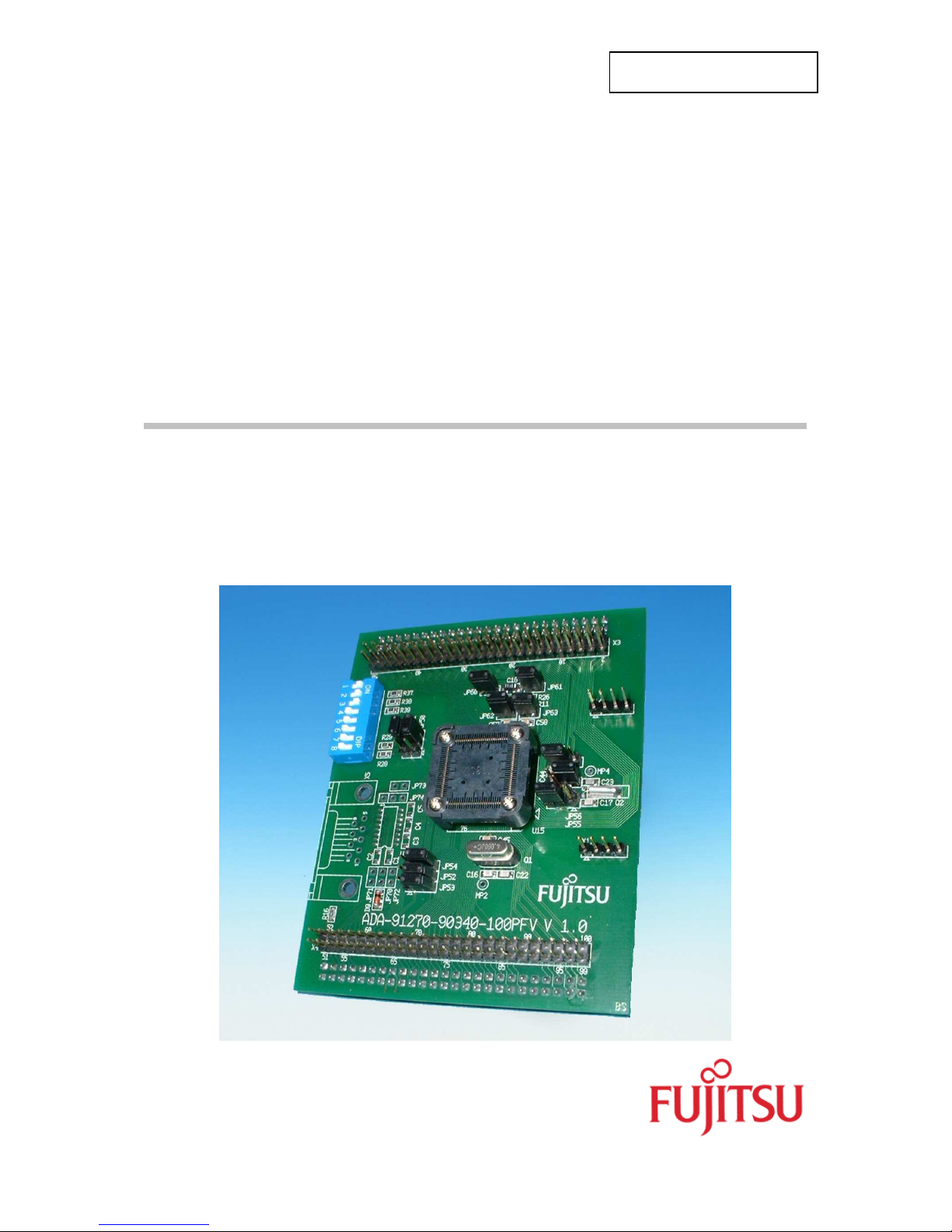
The ADA-91270-90340-100PFV is an adapter board that can be used together with the
evaluation board FLASH-CAN-100P-340 or as a stand-alone system with some limitations.
The ADA-91270-90340-100PFV supports devices of the 16-Bit MB90340 and MB96340
Series and 32-Bit MB91270 Series with LQFP package PFV/M05.
It can be used stand alone for software development and testing of with Flash-devices or as
a target board to work with the emulator system.
The board allows the designer immediately to start with the software development before his
own final target system is available.
2.2 Features of adapter board ADA-91270-90340-100PFV
< Supports the following series in FPT-100P-M05 package:
< MB90340 Series: MB90F34x PFV
< MB96340 Series: MB96F34x PFV (Please see chapter 7 for modification)
< MB91270 Series: MB91F272x PFV
< All resources available for evaluation
< All pins routed to connectors
< 4 MHz main-crystal, 32kHz subclock-crystal (selectable by jumpers)
< Run- / Program-Mode Selector
< One UART interface (optional)
2.3 Features supported by base-board FLASH-CAN-100P-340
< 9-12V unregulated external DC power supply usable
< 5V internal power supply, Power-LED
< In-Circuit serial Flash programming
< Two UART interfaces
< Two LIN interfaces
< Two High-Speed CAN Transceivers
< 8 User LEDs, optional: alphanumeric standard LC-Display connectable instead of LEDs
< Reset-Button, Reset-LED
< Up to 5 User-buttons
< 96 pin VG connector
The adapter board will be delivered with the MB91F272WPFV (dual clock version).
This microcontroller contains a 'burn-in'-boot loader for programming the flash.
This board must only be used for test applications
in an evaluation laboratory environment.
© Fujitsu Microelectronics Europe GmbH - 5 - UG-910012-16
Page 6
ADA-91270-90340-100PFV v1.0
JP50 P00/P10
Jumper 3 pol
1-2
JP51 P01/P11
Jumper 3 pol
1-2
JP52 SOT0/
SOT1 Jumper 2 pol
1-2
JP53 SIN0/SIN1
Jumper 2 pol
1-2
JP54 SCK0/SCK1
Jumper 2 pol
1-2
JP55 Subclock (X0A)
Jumper 4 pol
SUB
JP56 Subclock (X1A)
Jumper 3 pol
1-2
JP57 C-Pin Jumper 3 pol
1-2
JP60 AVSS
Jumper 2 pol
Closed
JP61 AVCC
Jumper 2 pol
Closed
JP62 AVRL Jumper 2 pol
Closed
JP63 AVRH
Jumper 2 pol
Closed
JP70 Optional: UTXD
Jumper 2 pol
Open
JP71 Optional: URXD
Jumper 2 pol
Open
JP72 Optional: URST
Jumper 2 pol
Open
JP73 Optional: RTS
-
CTS Jumper 2 pol
Open
JP74 Optional: URST
Jumper 3 pol
Open
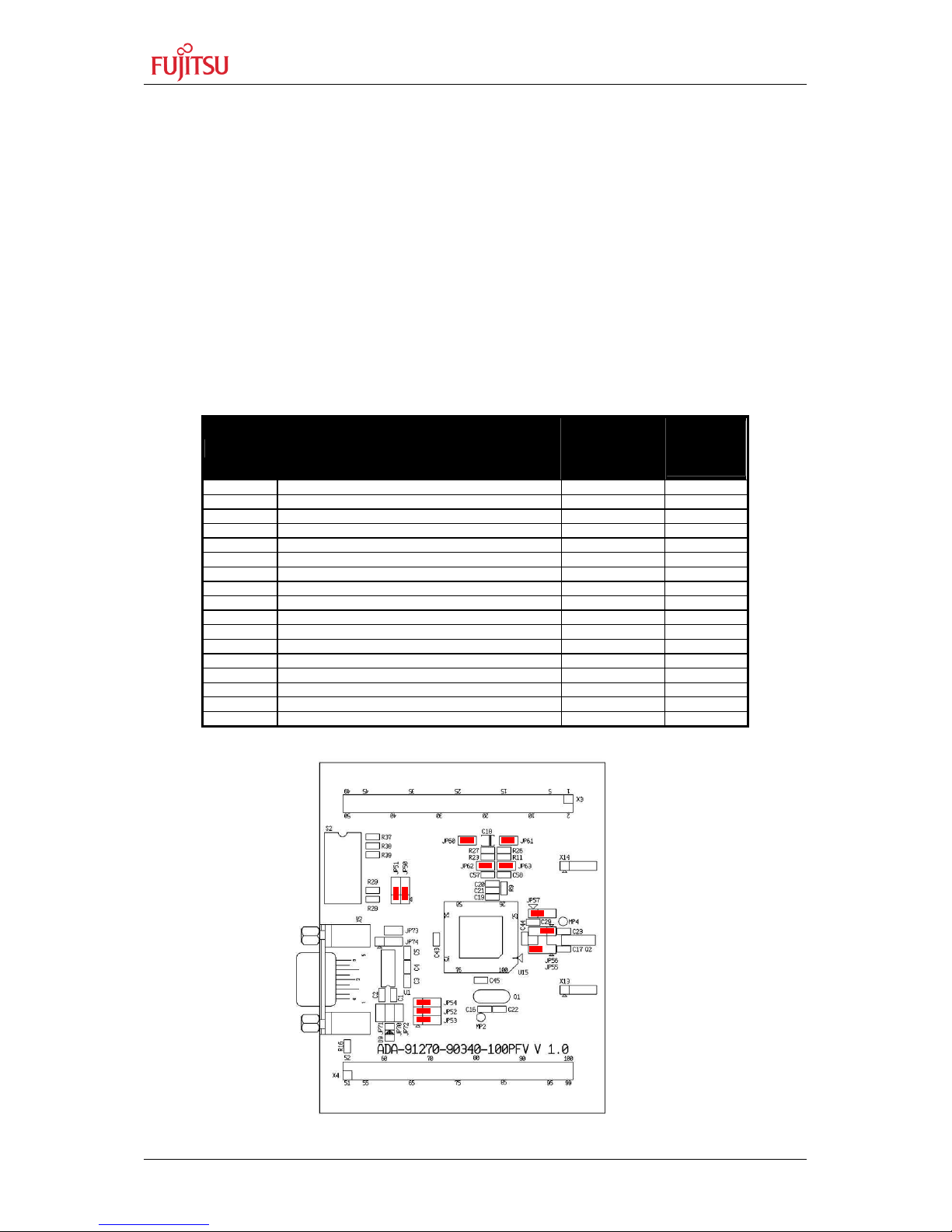
Chapter 3 Installation
3 Installation
Remove carefully the board from the shipping carton and check for any damages.
Make the correct jumper setting for the related device (MB90340 Series / MB96340 Series /
MB91270 Series). Please also see chapter 7 for board modification for MB96340 series.
The adapter board will be delivered with the MB91F272PFV microcontroller.
Before mounting the adapter on the FLASH-CAN-100P-340 remove the microcontroller and
check the correct jumper setting of the evaluation board. For details about the FLASH-CAN100P-340 evaluation board please see the user guide ug-900003.
3.1 MB90340 / MB96340 Series
The following default jumper setting of ADA-91270-90340-100PFV reflects a dual-clock
device of MB90340 / MB96340 Series. For details please refer to chapter 4.
Default
Jumper
Description / Function Type
MB90340
MB96340
UG-910012-16 - 6 - © Fujitsu Microelectronics Europe GmbH
Page 7
ADA-91270-90340-100PFV v1.0
J
P50 P00/P10
Jumper 3 pol
2-3
JP51 P01/P11
Jumper 3 pol
2-3
JP52 SOT0/SOT1
Jumper 2 pol
2-3
JP53 SIN0/SIN1
Jumper 2 pol
2-3
JP54 SCK0/SCK1
Jumper 2 pol
2-3
JP55 Subclock (X0A)
Jumper 4 pol
SUB
JP56 Subclock (X1A)
Jumper 3 pol
1-2
JP57 C-Pin Jumper 3
pol 1-2
JP60 AVSS
Jumper 2 pol
Closed
JP61 AVCC
Jumper 2 pol
Closed
JP62 AVRL Jumper 2 pol
Closed
JP63 AVRH
Jumper 2 pol
Closed
JP70 Optional: UTXD
Jumper 2 pol
Open
JP71 Optional: URXD
Jumper 2 pol
Open
JP72 Optional: URST
Jumper 2 pol
Open
JP73 O
ptional: RTS
-
CTS Jumper 2 pol
Open
JP74 Optional: URST
Jumper 3 pol
Open
Chapter 3 Installation
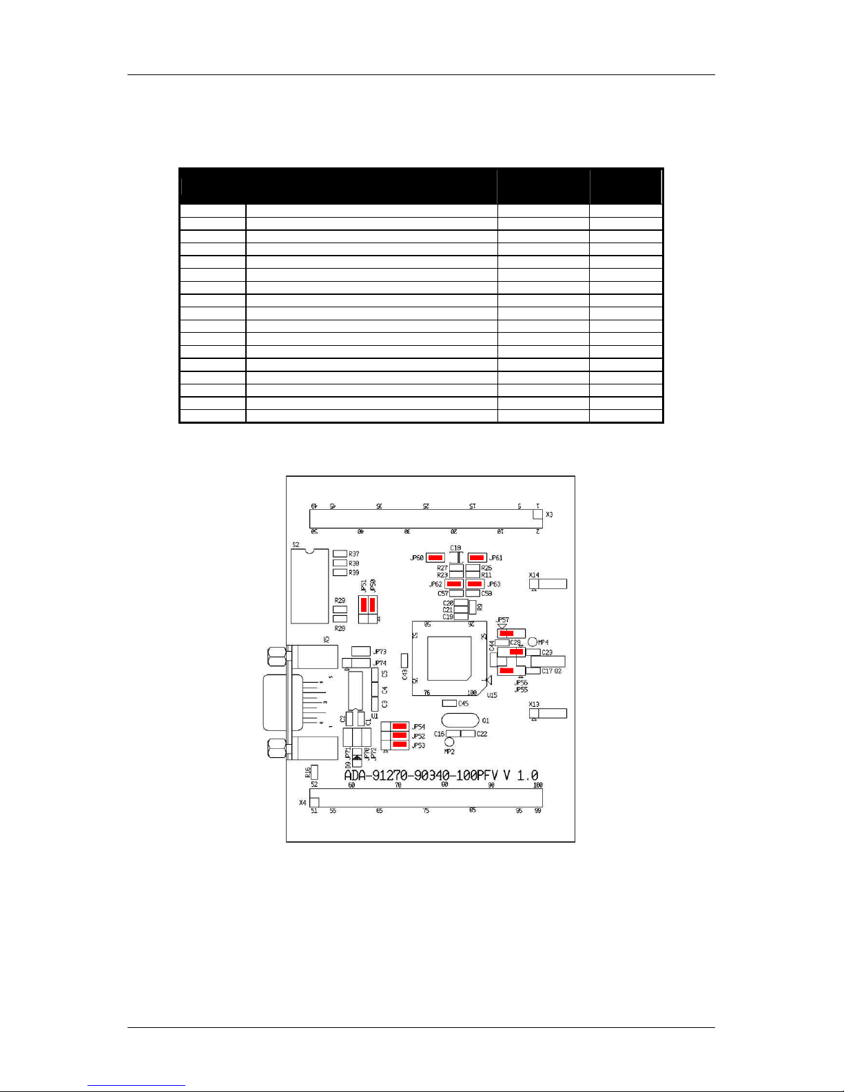
3.2 MB91270 Series
The following default jumper setting of ADA-91270-90340-100PFV reflects a dual-clock
device of MB91270 Series. For details please refer to chapter 4.
Jumper
Description / Function Type
Default
MB91270
© Fujitsu Microelectronics Europe GmbH - 7 - UG-910012-16
Page 8
ADA-91270-90340-100PFV v1.0
JP1a UART A (TXD) / UART0(MB90340)
Jumper 2 pol
Closed
D14
JP1b UART A (TXD) / UART0(MB90800) / SIO4(MB90945)
Jumper 2 pol
Open D14
JP1c UART A (TXD) / UART0(MB90945)
Jumper 2 po
l Open D14
JP2a UART A (RXD) / UART0(MB90340)
Jumper 2 pol
Closed
EF9
JP2b UART A (RXD) / UART0(MB90800) / SIO4(MB90945)
Jumper 2 pol
Open EF9
JP2c UART A (RXD) / UART0(MB90945)
Jumper 2 pol
Open EF10
JP3 DTR/RTS A
Jumper 3 pol
Open D4
JP4 RESET UART
A/B Jumper 3 pol
Open E10
JP5 DTR/RTS B
Jumper 3 pol
Open D8
JP6a UART B (RXD) / UART2(MB90340)
Jumper 2 pol
Closed
EF12
JP6b UART B (RXD) / UART1(MB90800)
Jumper 2 pol
Open EF12
JP6c UART B (RXD) / UART3(MB90945)
Jumper 2 pol
Open EF13
JP8a UART B (T
XD) / UART2(MB90340)
Jumper 2 pol
Closed
EF11
JP8b UART B (TXD) / UART1(MB90800)
Jumper 2 pol
Open EF11
JP8c UART B (TXD) / UART3(MB90945)
Jumper 2 pol
Open EF12
JP7 Reset 3V3
Jumper 2 pol
Open E8
JP9 LIN B enable
Jumper 2 pol
Open G13
JP10 LIN B Mast
er-Mode Jumper 2 pol
Open E3
JP11 AVcc Jumper 2 pol
Closed
K21
JP12 SW1 Jumper 2 pol
Closed
G9
JP13 AVcc=AVRH
Jumper 2 pol
Closed
J21
JP14 SW2 Jumper 2 pol
Closed
G9
JP15 AVss Jumper 2 pol
Closed
K19
91270: Open
JP17 LIN A enable
Jumper 2 pol
Open H13
JP18 LIN A Master
-
Mode Jumper 2 pol
Open H3
JP19 AVSS=AVRL
Jumper 2 pol
Closed
J20
JP20 SW4 Jumper 2 pol
Closed
F9
JP21a
LIN A (RXD) / LINUART1(90340)
Jumper 2 pol
Open H13
JP21c
LIN A (RXD) / LINUART3(90945)
Jumper 2 pol
Open H13
JP22a
LIN A (TXD) / LINUART1(90340)
Jumper 2 pol
Open H13
JP22c
LIN A (TXD) / LINUART3(90945)
Jumper 2 pol
Open H13
JP23 SW5 Jumper 2 pol
Closed
F9
JP24 RESET
Jumper 2 pol
Closed
E8
JP25 CAN A (TXD) / CAN0(MB90340)
Jumper 2 pol
Closed
J13
JP26 CAN A (RXD) / CAN0(MB90340)
Jumper 2 pol
Closed
J13
JP27a
CAN B (TXD) / CAN1(MB90340)
Jumper 2 pol
Open J13
JP27c
CAN B (TXD) / CAN1(MB90945)
Jumper 2 pol
Open J13
JP28a
CAN B (TXD) / CAN1(MB90340)
Jumper 2 pol
Open K13
JP28c
CAN B (RX
D) / CAN1(MB90945)
Jumper 2 pol
Open K13
JP29 int/ext VCC
Jumper 3 pol
1-2
J17
JP30 5V/3V3
Jumper 2 pol
Open L15
JP31 RTS-CTS A
Jumper 2 pol
Closed
D4
JP32 RTS-CTS B
Jumper 2 pol
Closed
D8
JP33 C-Pin to MCU_VCC
sold-Jumper
Open H22
JP34 MCU_VCC
Jumpe
r 2pol Closed
J17
JP35 DTR / DTRx
Jumper 3 pol
Open F11
JP36 X0A select
Jumper 4 pol
1-4
G22
JP37 X1A select
Jumper 3 pol
1-2
G22
JP38 LIN B (RXD) / LINUART3(90340)
Jumper 2 pol
Open F12
JP39 LIN B (TXD) / LINUART3(90340)
Jumper 2 pol
Open F12
JP40 C-Pin Jumper 2 pol
Closed
GH22
JP41 P00/P65
Jumper 3 pol
1-2
E17
JP42 P01/P66
Jumper 3 pol
1-2
E17
JP43a
SCK0(MB90340)
Jumper 2 pol
Closed
D16
JP43b
SCK0(MB90800) / SCK4(MB90945)
Jumper 2 pol
Open D16
JP44 SIN_A
Jumper 2 pol
Closed
EF9
Chapter 3 Installation
3.3 Jumper settings of FLASH-CAN-100P-340
The following jumper setting should be chosen if the FLASH-CAN-100P-340 V1.1 board is
used together with ADA-91270-90340-100PFV:
Default
Jumper
Description / Function Type
ADA-91270-
90340-100PFV
Coordinates
JP16 SW3 Jumper 2 pol
90340: Closed
G9
UG-910012-16 - 8 - © Fujitsu Microelectronics Europe GmbH
Page 9

ADA-91270-90340-100PFV v1.0
CAN0
(LIN
-
(LIN
-
CAN1
Chapter 3 Installation
A B C D E F G H J K L M N
1
2
3
4
5
6
7
8
9
10
11
12
13
14
15
16
1
2
UART3)
UART1)
3
4
5
6
7
8
9
10
11
12
13
14
15
16
17
18
19
20
21
22
23
24
25
26
27
17
18
19
20
21
22
23
24
25
26
27
A B C D E F G H J K L M N
Please see the user guide ug-900003 for a detailed description of the FLASH-CAN100P-340
evaluation board.
© Fujitsu Microelectronics Europe GmbH - 9 - UG-910012-16
Page 10

ADA-91270-90340-100PFV v1.0
RUN mode
1 2 3 4 5 6 7 8
MD0 MD1 MD2 nc nc nc P01 P00
1 2 3 4 5 6 7 8
MD0 MD1 MD2 nc nc nc P11 P10
Chapter 4 Jumpers and Switches
4 Jumpers and Switches
This chapter describes all jumpers and switches that can be modified on the adapter board.
The default setting (MB91270 Series) is shown with a grey shaded area. All jumpers and
switches are named directly on the board, so it is very easy to set the jumpers according to
the features.
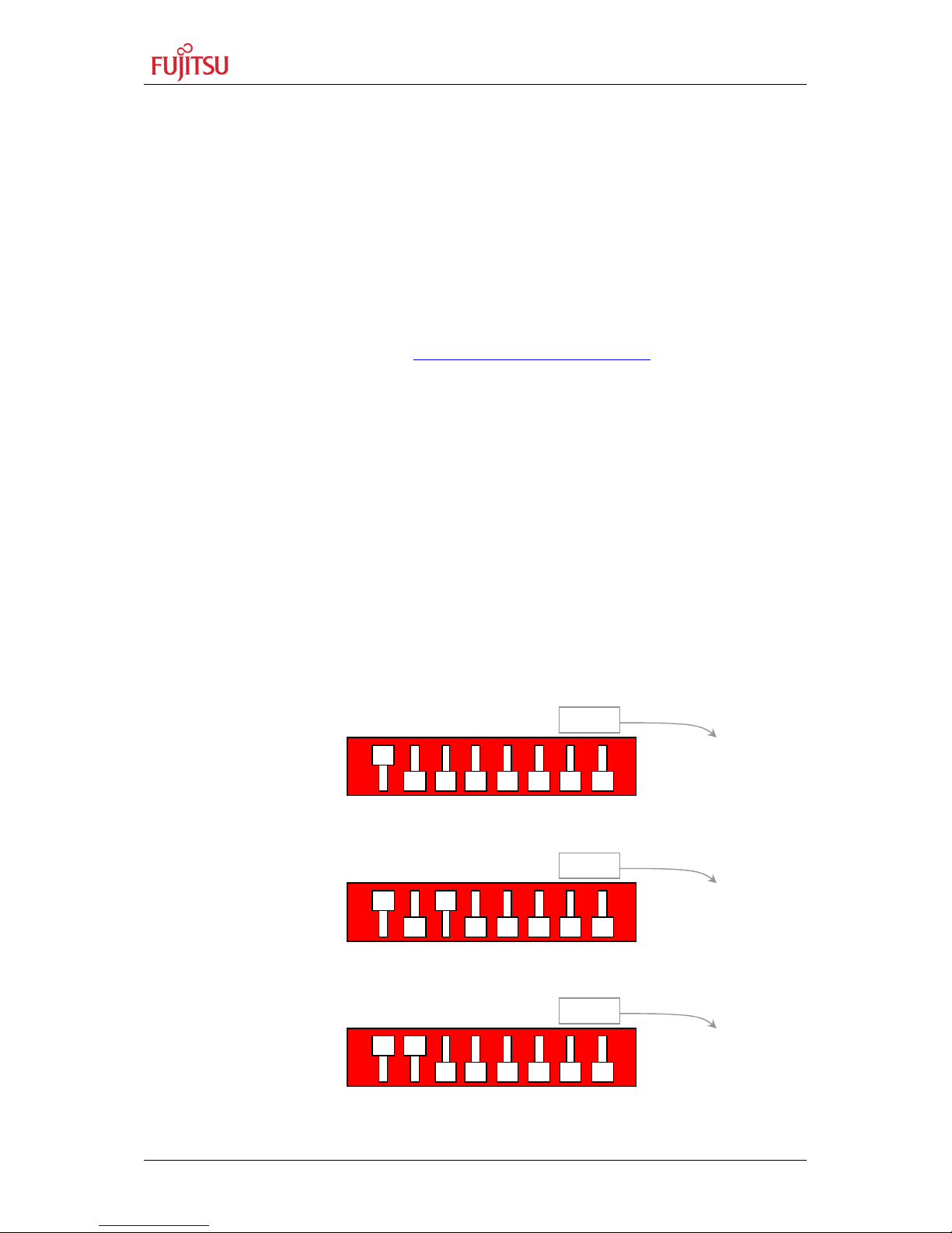
4.1 Operating-Mode (S2)
The DIP-switch S2 is used to set the operating mode of the µC. Ensure that the mode pin
settings correspond to the operation-mode of the application. For more detailed information
please check the Hardware-Manual of the microcontroller.
DIP switch Setting Logical value
S2/1 (MD0)
ON (closed) 0 (low)
OFF (open) 1 (high)
S2/2 (MD1)
ON (closed) 0 (low)
OFF (open) 1 (high)
S2/3 (MD2)
ON (closed) 0 (low)
OFF (open) 1 (high)
S2/4-6 not connected (OFF)
S2/7 (P01/P11*)
ON (closed) 1 (high)
OFF (open) 0 (low) *1
S2/8 (P00/P11*)
ON (closed)
OFF (open)
*1Note: The low-level for serial programming is reached by the pull-down resistors R28 and R29 that are enabled by the
jumpers JP50 and JP51. Please refer to chapter 5 (Programming the internal Flash) for more details about the operation mode.
1 (high)
0 (low) *1
4.1.1 MB90340 / MB96340 Series
Dip-Switch S2
MB90340 / MB96340
ON
OFF
Note:
JP50: 1-2
JP51: 1-2
4.1.2 MB91270 Series
Dip-Switch S2
MB91270 RUN mode
UG-910012-16 - 10 - © Fujitsu Microelectronics Europe GmbH
ON
OFF
Note:
JP50: 2-3
JP51: 2-3
Page 11
ADA-91270-90340-100PFV v1.0
Chapter 4 Jumpers and Switches
4.2 Analogue Power Supply Voltage (JP: 60, 61, 62, 63)
The power supply as well as the positive reference voltage for the A/D-converter can be
provided internally or externally.
JP60, JP61 connect power supply voltages (AVcc and AVss)
JP62, JP63 connect reference voltages (AVRH to AVcc, ARRL to AVss)
Jumper Setting Description
ON (closed) AVss is connected to GND
JP60 (AVss)
OFF (open) AVss is disconnected from GND
ON (closed) AVcc is connected to Vcc
JP61 (AVcc)
OFF (open) AVcc is disconnected from Vcc
ON (closed) AVRL is connected to AVss
JP62 (AVRL)
OFF (open) AVRL defined by resistor network*1
ON (closed) AVRH is connected to AVcc
JP63 (AVRH)
OFF (open) AVRH defined by resistor network*1
*1
By default the resistor network (R11, R23 and R26, R27) is not mounted on the board
Default: JP60, JP61, JP62 and JP63 are closed
By default, the A/D-converter supply and reference voltage is same as the microcontroller
supply voltage.
Note:
If JP60 and J61 are open, the user has to supply an adequate analogue voltage supply
(AVcc and AVss) to the A/D-converter.
If JP63 is open, the resistors R11 and R23 define AVRH.
If JP62 is open, the resistors R26 and R27 define AVRL.
By default the resistor network (R11, R23 and R26, R27) is not mounted on the board.
© Fujitsu Microelectronics Europe GmbH - 11 - UG-910012-16
Page 12

ADA-91270-90340-100PFV v1.0
Pin-out JP55:
Chapter 4 Jumpers and Switches
4.3 Subclock (JP: 55,56)
Some devices support a 32 kHz subclock (X0A, X1A), other devices do not support a
subclock but will offer additional port-pins (e.g. P40, P41) instead.
Please check the related datasheet.
JP55: defines usage of microcontroller pin 11 (X0A/P40)
JP56: defines usage of microcontroller pin 12 (X1A/P41)
Jumper Setting Description
SUB - Pin11 Pin 11 is connected to the 32 kHz Subclock (X0A)
JP55 (X0A/P40)
P40 - Pin11 Pin 11 is used as P40 and is connected to X3-11
GND - Pin11
Pin 11 is connected to GND (in case that subclockdevice is used, but no 32kHz crystal is connected)
1-2 Pin 12 is connected to the 32kHz Subclock (X1A)
JP56 (X1A/P41)
2-3 Pin 12 is used as P41 and is connected to X3-12
Default: JP55: 1-4, JP56: 1-2
By default, the 32kHz-subclock-crystal is connected to the microcontroller.
P40
GND
Pin11
SUB
UG-910012-16 - 12 - © Fujitsu Microelectronics Europe GmbH
Page 13
ADA-91270-90340-100PFV v1.0
Chapter 4 Jumpers and Switches
4.4 UART”A” (JP: 52, 53, 54)
Because MB90340, MB96340, and MB91270 Series uses different UARTs for the burn-in
bootloader the right UART can be connected to UART “A” and the programming socket X17
for synchronous programming of the FLASH-CAN-100P-340 evaluation board:
MB90340 and MB96340 Series use UART0 for in circuit programming.
MB91270 Series uses UART1 for in circuit programming.
JP52 connects SOT0 or SOT1 to UART “A” and to X17 (FlashKit)
JP53 connects SIN0 or SIN1 to UART “A” and to X17 (FlashKit)
JP54 connects SCK0 or SCK1 to UART “A” and to X17 (FlashKit)
Jumper Setting Description
1-2 SOT0
(MB90340 bootloader UART)
is connected to UART ‘A’
JP52 (SOTx)
2-3*1 SOT1
1-2 SIN0
(MB91270 bootloader UART)
(MB90340 bootloader UART)
is connected to UART ‘A’
is connected to UART ‘A’
JP53 (SINx)
2-3*1 SIN1
1-2 SCK0
(MB91270 bootloader UART)
(MB90340 bootloader UART)
is connected to UART ‘A’
is connected to UART ‘A’
JP54 (SCKx)
2-3*1 SCK1
(MB91270 bootloader UART)
is connected to UART ‘A’
Default: JP52=2-3, JP53=2-3, JP54=2-3
By default, UART1 is used as UART”A”.
*1
Note for MB91270 Series:
Make sure that jumper JP21a and JP22a (LIN transceiver) on the FLASH-CAN-100P-340
are open, while the UART1 of MB91270 Series is used.
© Fujitsu Microelectronics Europe GmbH - 13 - UG-910012-16
Page 14
ADA-91270-90340-100PFV v1.0
1 2 3 4 5 6 7 8
MD0 MD1 MD2 nc nc nc P01 P00
MD0 MD1 MD2 nc nc nc P11 P10
1 2 3 4 5 6 7 8
MD0 MD1 MD2 nc nc nc P01 P00
Chapter 5 Programming the internal Flash
5 Programming the internal Flash
All Flash devices have an internal bootloader for asynchronous- as well as synchronousFlash-programming:
< asynchronous-serial Flash-programming via X3 (UART “A”) of FLASH-CAN-100P-340
<
synchronous-serial Flash-programming via X17 (“FlashKit”) of FLASH-CAN-100P-340
5.1 Asynchronous Mode
The Flash-microcontroller of MB90340, MB96340, and MB91270 Series can be programmed
in circuit by using the freeware “Fujitsu Flash MCU Programmer” that is available on the
Fujitsu Micros CD-ROM or Web Site (http://www.fme.gsdc.de/gsdc.htm: select < Software <
Utilities)
MB90340 and MB96340 Series use UART0 for in circuit programming.
Note: Basically MB96340 supports programming via UART0-URAT3
MB91270 Series uses UART1 for in circuit programming.
Note: Open jumper JP16 of FLASH-CAN-100P-340 because P10 is used for mode selection.
Please check the correct UART selection in chapter 4.4.
The following procedure must be followed to enable Flash Programming:
1. Power off the system
2. Connect the Evaluation Board UART”A” to your serial PC communication port.
A straight cable connection (1:1) has to be used.
3. Check the Jumper-settings according to the UART as described in chapter 4.4.
4. Configure by Dip-Switch S2 the mode related to your microcontroller:
MB90340
PGM mode
ON
OFF
MB96340
PGM mode
ON
OFF
Note:
JP50: 1-2
JP51: 1-2
Note:
JP50: 1-2
JP51: 1-2
MB91270
PGM mode
UG-910012-16 - 14 - © Fujitsu Microelectronics Europe GmbH
1 2 3 4 5 6 7 8
Note:
ON
JP50: 2-3
OFF
JP51: 2-3
Flash-CAN-100P-340:
JP16: open
Page 15

ADA-91270-90340-100PFV v1.0
1 2 3 4 5 6 7 8
MD0 MD1 MD2 nc nc nc P01 P00
1 2 3 4 5 6 7 8
MD0 MD1 MD2 nc nc nc P11 P10
Chapter 5 Programming the internal Flash
5. Power on the board
6. Check that the Reset LED is off. Otherwise change the DTR polarity (JP35) and check
the power supply voltage.
7. Start the tool “Fujitsu Flash MCU Programmer” software and follow the instructions:
Note: The screenshot may differ regarding the used release version of the tool
Select Crystal
Set Device Type
MB90F347
Select COM Port
Open Source
(MHX-File)
Start
programming
8. After programming the Flash-ROM, switch off the power supply and set back the mode
according to the usage of the application, e.g.:
MB90340
MB96340
RUN mode
MB91270
RUN mode
9. Power on the board. The user application is started directly.
ON
OFF
ON
OFF
Note:
JP50: 1-2
JP51: 1-2
Note:
JP50: 2-3
JP51: 2-3
© Fujitsu Microelectronics Europe GmbH - 15 - UG-910012-16
Page 16

ADA-91270-90340-100PFV v1.0
Chapter 6 Connectors
6 Connectors
6.1 Edge connector (X3, X4)
Nearly*1 all pins of the microcontroller are directly connected to X3 and X4 as follows:
Connector*1 MCU Pins*1
X3 (1 – 50) 1 – 50
X4 (51 – 100) 51 – 100
The odd pin numbers are located on the one side and the even pin numbers are located on
the other side of the connector.
On the PCB, the corresponding pin numbers of the µC are written next to the connector pins.
*1
Note:
The following pins are not routed to the connecter (X3, X4):
Pin 13 (VCC) Pin 14 (GND) Pin 42 (GND) Pin 63 (VCC)
Pin 64 (GND) Pin 88 (VCC) Pin 89 (GND) Pin 90 (X1)
Pin 91 (X0)
UG-910012-16 - 16 - © Fujitsu Microelectronics Europe GmbH
Page 17

Chapter 7 Board Modification for MB96340 Series
ADA-91270-90340-100PFV v1.0
7 Board Modification for MB96340 Series
For the MB9634x series an additional 10µF capacitor for the C pin is needed to be soldered
on the board. Please see the following photograph of the backside of the board for a
possible connection:
The positive pole of the capacitor is connected to the middle pin of jumper JP57. The
negative pole is connected to a ground pin of connector X14.
© Fujitsu Microelectronics Europe GmbH - 17 - UG-910012-16
Page 18

ADA-91270-90340-100PFV v1.0
optional: LCD
Chapter 8 Silk-Plot of the Board
8 Silk-Plot of the Board
X4
VG96-male
FlashKit
CAN”B”
X11
CAN”A”
X10
X12
Power-
MAX232
MAX232
User-LEDs (P00-P07)
SW1 SW2 SW3 SW4 SW5 Reset
LIN”A”
LIN”B”
X17
UART”B”
X5
UART”A”
X3
UG-910012-16 - 18 - © Fujitsu Microelectronics Europe GmbH
X8
X6
Page 19

Chapter 9 Notes on using the ADA-91270-90340-100PFV V1.0
ADA-91270-90340-100PFV v1.0
9 Notes on using the ADA-91270-90340-100PFV V1.0
9.1 Stand-alone mode
The MB91F272 does not have an internal power-on reset circuitry. Therefore, when using
the MB91F272 on the ADA-91270-90340-100PFV in stand-alone mode, a reset must be
generated externally after powering-up the board.
9.2 PCB History
Part Problem Fixed
JP55 Pin11 and GND are swapped in the layout Patched
S2 Dip-Switch pins may be shorted by heat-sink of U9 (FLASH-CAN-100P-340) -
C29
For use with MB96340 an additional capacitor (C29A=10uF) has to be soldered.
(See chapter 7 for details)
-
© Fujitsu Microelectronics Europe GmbH - 19 - UG-910012-16
Page 20

ADA-91270-90340-100PFV v1.0
Chapter 10 Related Products
10 Related Products
< FLASH-CAN-100P-340 Evaluation board for
MB90340, MB90800, MB90860, MB90945 Series
with FPT-100P-M06 package
< ADA-91270-90340-100PFV Adapterboard for M05 (PFV) Package of
MB90340, MB96340, and MB91270 Series
< NQPack100SD-ND Socket for package FPT-100P-M05
(Tokyo Eletech Corp. www.tetc.co.jp/e_tet.htm)
< HQPack100SD Header for NQPack100SD-ND
< MB90340 Series
< MB90F34xS_PFV Flash-MCU (M05 package), single-clock
< MB90F34x_PFV Flash-MCU (M05 package), dual-clock
< MB2147-01 Emulator debugger main unit
< MB2147-20 Emulation adapter
< MB90V340A-101 Evaluation chip for MB90340 Series, single-clock
< MB90V340A-102 Evaluation chip for MB90340 Series, dual-clock
< MB90V340A-103 Eval.-chip for MB90340 Series, single-clock, incl. RC-osc
< MB90V340A-104 Eval.-chip for MB90340 Series, dual-clock, incl. RC-osc
< MB2147-581 Emulator probe cable for MB90340/M05 Package
< MB96340 Series
< MB96F34x_PFV Flash-MCU (M20 package)
< MB2198-01 Emulator debugger main unit
< MB2198-500 Emulation adapter
< MB96V300 Evaluation chip for MB96340 Series
< MB91270 Series
< MB91F27xS_PFV Flash-MCU (M05 package), single-clock
< MB91F27x_PFV Flash-MCU (M05 package), dual-clock
< MB2198-01 Emulator debugger main unit
< MB2198-10 Emulator DSU cable
< MB2198-130 Emulation POD
< MB91V280CR-ES Evaluation chip for MB91270 Series, single-clock
< MB2198-129 Emulator probe cable for MB91270/M05 Package
UG-910012-16 - 20 - © Fujitsu Microelectronics Europe GmbH
Page 21

ADA-91270-90340-100PFV v1.0
Chapter 11 Information in the WWW
11 Information in the WWW
Information about FUJITSU MICROELECTRONICS Products
can be found on the following Internet pages:
Microcontrollers (8-, 16- and 32bit), Graphics Controllers
Datasheets and Hardware Manuals, Support Tools (Hard- and Software)
http://www.fme.gsdc.de/gsdc.htm
Linear Products: Power Management, A/D and D/A Converters
http://www.fujitsu.com/emea/services/microelectronics/linears/
Media Products: SAW filters, acoustic resonators and VCOs
http://www.fujitsu.com/emea/services/microelectronics/saw/
For more information about FUJITSU MICROELECTRONICS
http://www.fujitsu.com/emea/services/microelectronics/
© Fujitsu Microelectronics Europe GmbH - 21 - UG-910012-16
Page 22

ADA-91270-90340-100PFV v1.0
Chapter 12 China-RoHS regulation
12 China-RoHS regulation
Evaluation Board
Emulation Board
根据SJ/T11364-2006
《电子信息产品污染控制标识要求》特提供如下有关污染控制方面的信息。
The following product pollution control information is provided according to SJ/T11364-2006
Marking for Control of Pollution caused by Electronic Information Products.
1.电子信息产品污染控制标志说明 Explanation of Pollution Control Label
评估板
仿真板
该标志表明本产品含有超过中国标准SJ/T11363-2006
《电子信息产品中有毒有害物质的限量要求》中限量的有毒有害物质。标志中的数字为本产品
的环保使用期,表明本产品在正常使用的条件下,有毒有害物质不会发生外泄或突变,用户使
用本产品不会对环境造成严重污染或对其人身、财产造成严重损害的期限,单位为年。
为保证所申明的环保使用期限,应按产品手册中所规定的环境条件和方法进行正常使用,并严
格遵守产品维修手册中规定的定期维修和保养要求。
产品中的消耗件和某些零部件可能有其单独的环保使用期限标志,并且其环保使用期限有可能
比整个产品本身的环保使用期限短。应到期按产品维修程序更换那些消耗件和零部件,以保证
所申明的整个产品的环保使用期限。
本产品在使用寿命结束时不可作为普通生活垃圾处理,应被单独收集妥善处理。
请注意:环保使用期限50年的指定不是与产品的耐久力,使用期限或任何担保要求等同的。
This symbol to be added to all EIO sold to China, indicates the product contains hazardous
materials in excess of the limits established by the Chinese standard SJ/T11363-2006
Requirements for Concentration Limits for Certain Hazardous Substances in Electronic
Information Products. The number in the symbol is the Environment-friendly Use Period
(EFUP), which indicates the period, starting from the manufacturing date, during which the
toxic or hazardous substances or elements contained in electronic information products will
not leak or mutate under normal operating conditions so that the use of such electronic
information products will not result in any severe environmental pollution, any bodily injury or
damage to any assets, the unit of the period is “Year”.
UG-910012-16 - 22 - © Fujitsu Microelectronics Europe GmbH
Page 23

ADA-91270-90340-100PFV v1.0
Chapter 12 China-RoHS regulation
In order to maintain the declared EFUP, the product shall be operated normally according to
the instructions and environmental conditions as defined in the product manual, and periodic
maintenance schedules specified in Product Maintenance Procedures shall be followed
strictly.
Consumables or certain parts may have their own label with an EFUP value less than the
product. Periodic replacement of those consumables or parts to maintain the declared EFUP
shall be done in accordance with the Product Maintenance Procedures.
This product must not be disposed of as unsorted municipal waste, and must be collected
separately and handled properly after decommissioning.
Please note: The designation of 10 years EFUP is not to be equated with the durability, useduration or any warranty-claims of the product.
产品中有毒有害物质或元素的名称及含量
Table of hazardous substances name and concentration
部件
部件
名称
名称
部件部件
名称名称
Component Name
有毒有害物质
有毒有害物质
有毒有害物质有毒有害物质
Hazardous substances name
或元素
或元素
或元素或元素
ADA-91270-90340-
100PFV v1.0
铅铅铅铅
(Pb)
x o o o o o
汞汞汞汞
(Hg)
镉镉镉镉
(Cd)
六价铬
六价铬
六价铬六价铬
(Cr(VI))
多溴联苯
多溴联苯
多溴联苯多溴联苯
(PBB)
多溴二苯醚
多溴二苯醚
多溴二苯醚多溴二苯醚
(PBDE)
O: 表示该有毒有害物质在该部件所有均质材料中的含量均在
表示该有毒有害物质在该部件所有均质材料中的含量均在SJ/T11363-2006 标准规定的限量要求以下
表示该有毒有害物质在该部件所有均质材料中的含量均在表示该有毒有害物质在该部件所有均质材料中的含量均在
X: 表示该有毒有害物质至少在该部件的某一均质材料中的含量超出
表示该有毒有害物质至少在该部件的某一均质材料中的含量超出SJ/T11363-2006 标准规定的限量要求
表示该有毒有害物质至少在该部件的某一均质材料中的含量超出表示该有毒有害物质至少在该部件的某一均质材料中的含量超出
标准规定的限量要求以下
标准规定的限量要求以下标准规定的限量要求以下
标准规定的限量要求
标准规定的限量要求标准规定的限量要求
• 此表所列数据为发布时所能获得的最佳信息
•
由于缺少经济上或技术上合理可行的替代物质或方案,此医疗设备运用以上一些有毒有害物质来实现设备的
预期临床功能,或给人员或环境提供更好的保护效果
。
O: Indicates that this toxic or hazardous substance contained in all of the homogeneous
materials for this part is below the limit requirement in SJ/T11363-2006.
X: Indicates that this toxic or hazardous substance contained in at least one of the
homogeneous materials used for this part is above the limit requirement in SJ/T11363-2006.
• Data listed in the table represents best information available at the time of publication
© Fujitsu Microelectronics Europe GmbH - 23 - UG-910012-16
Page 24

ADA-91270-90340-100PFV v1.0
Chapter 13 Recycling
13 Recycling
Gültig für EU-Länder:
Gemäß der Europäischen WEEE-Richtlinie und deren Umsetzung in landesspezifische
Gesetze nehmen wir dieses Gerät wieder zurück.
Zur Entsorgung schicken Sie das Gerät bitte an die folgende Adresse:
Fujitsu Microelectronics Europe GmbH
Warehouse/Disposal
Monzastraße 4a
63225 Langen
Valid for European Union Countries:
According to the European WEEE-Directive and its implementation into national laws we
take this device back.
For disposal please send the device to the following address:
Fujitsu Microelectronics Europe GmbH
Warehouse/Disposal
Monzastraße 4a
63225 Langen
UG-910012-16 - 24 - © Fujitsu Microelectronics Europe GmbH
 Loading...