

Page 1
1. PICTURE TUBE
Size : 17 inch (Flat Slot Mask)
DefIection Angle : 90°
Neck Diameter : 29.1mm
Stripe Pitch : 0.24mm
Face Treatment : W-ARAS(Anti-Reflection and
Anti-Static Coating)
Internal : Anti-Glare
2. SIGNAL
2-1. Horizontal & Vertical Sync
1) Input Voltage Level: Low=0~1.2V, High=2.5~5.5V
2) Sync Polarity : Positive or Negative
2-2. Video Input Signal
1) Voltage Level : 0 ~ 0.7 Vp-p
a) Color 0, 0 : 0 Vp-p
b) Color 7, 0 : 0.467 Vp-p
c) Color 15, 0 : 0.7 Vp-p
2) Input Impedance : 75Ω
3) Video Color : R, G, B Analog
4) Signal Format : Refer to the Timing Chart
2-3. Signal Connector
15-pin Attached Connector
2-4. Scanning Frequency
Horizontal : 30 ~ 72 kHz
Vertical : 50 ~ 160 Hz
3. POWER SUPPLY
3-1. Power Range
AC200~240V(PFC) 50Hz, 1.5A
3-2. Power Consumption
4. DISPLAY AREA
4-1. Active Video Area :
• Max Image Size - 325.4 x 244.1mm (12.81" x 9.61")
• Preset Image Size - 310 x 230 mm (12.20" x 9.06")
4-2. Display Color : Full Colors
4-3. Display Resolution : 1280 x 1024 / 60Hz
(Non-Interlace)
4-4. Video Bandwidth : 110MHz
5. ENVIRONMENT
5-1. Operating Temperature: 10°C ~ 35°C (Ambient)
5-2. Relative Humidity : 10% ~ 90%
(Non-condensing)
5-3. Altitude : 5,000m
6. DIMENSIONS (with TILT/SWIVEL)
Width : 415.0mm (16.34 inch)
Depth : 439.0mm (17.28 inch)
Height : 435.0mm (17.13 inch)
7. WEIGHT (with TILT/SWIVEL)
Net Weight : 17.8kg (39.24 lbs.)
Gross Weight : 20.0kg (44.09 lbs.)
- 2 -
MODE
NORMAL (ON)
STAND-BY
SUSPEND
OFF
H/V SYNC
ON/ON
OFF/ON
ON/OFF
OFF/OFF
POWER CONSUMPTION
less than 105W
less than 15W
less than 15W
less than 5W
LED COLOR
GREEN
AMBER
AMBER
SPECIFICATIONS
Page 2
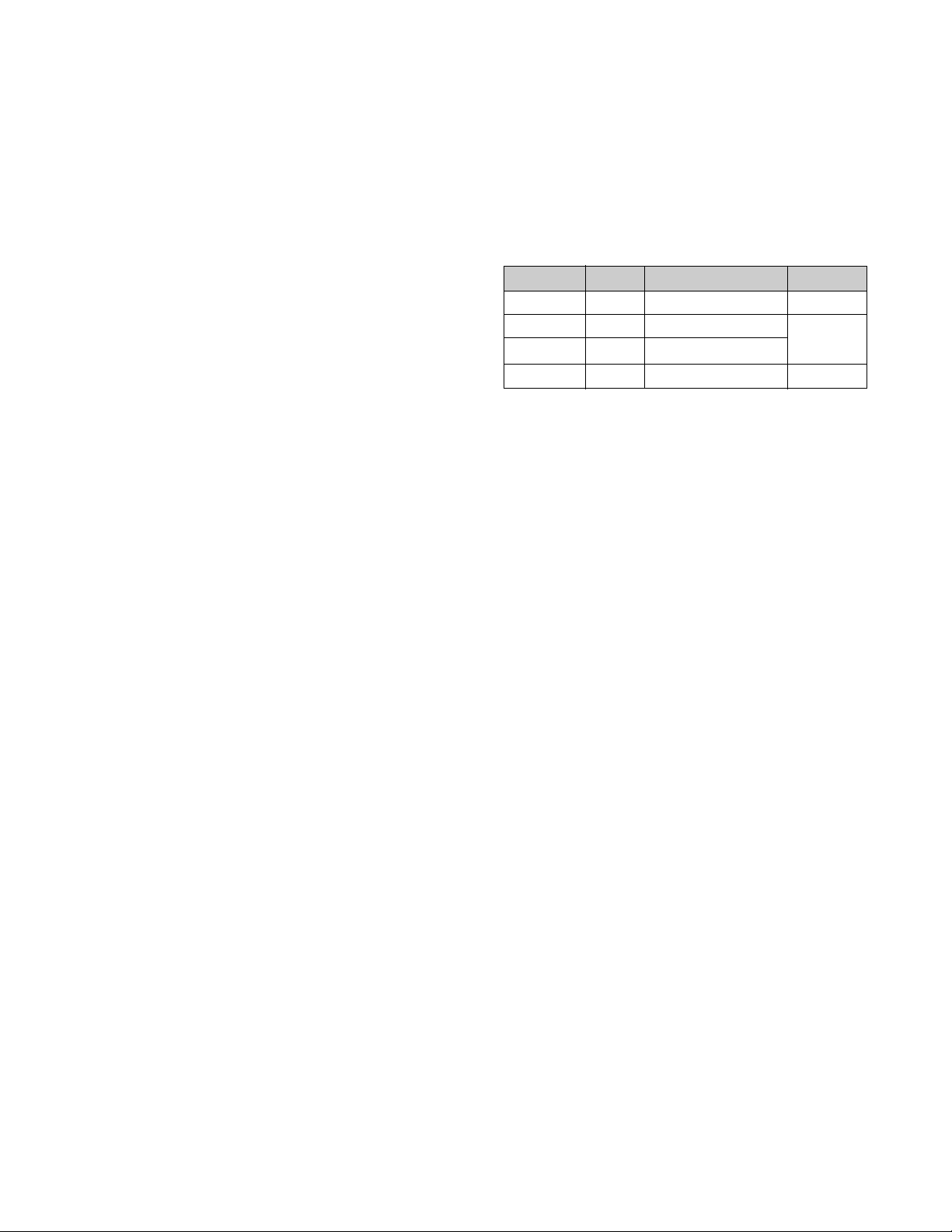
TIMING CHART
- 4 -
VIDEO
SYNC
C
E
D
F
AB
MODE
Resolution
Recall
H
O
R
I
Z
O
N
T
A
L
V
E
R
T
I
C
A
L
kHz
µs
µs
µs
µs
µs
µs
Hz
ms
ms
ms
ms
ms
ms
MODE 5
+
46.88
21.33
16.16
5.17
0.32
1.62
3.23
+
75.0
13.333
12.80
0.5333
0.021
0.064
0.448
800
x
600
75Hz
Yes
MODE 3
—
37.50
26.67
20.32
6.35
0.51
2.03
3.81
—
75.0
13.333
12.80
0.533
0.027
0.080
0.427
640
x
480
75Hz
Yes
MODE 6
+
53.67
18.63
14.22
4.41
0.57
1.14
2.70
+
85.06
11.756
11.179
0.578
0.019
0.056
0.503
800
x
600
85Hz
Yes
MODE 8
+
68.677
14.561
10.836
3.725
0.508
1.016
2.201
+
85.00
11.765
11.183
0.582
0.015
0.044
0.524
1024
x
768
85Hz
Yes
MODE 1
—
31.47
31.77
25.42
6.36
0.64
3.81
1.91
+
70.1
14.267
12.710
1.557
0.413
0.064
1.080
720
x
400
70Hz
Yes
MODE 2
—
31.47
31.78
25.42
6.36
0.64
3.81
1.91
—
59.9
16.683
15.253
1.430
0.318
0.064
1.049
640
x
480
60Hz
Yes
MODE 4
—
43.269
23.111
17.778
5.333
1.556
1.556
2.222
—
85.0
11.764
11.093
0.670
0.023
0.069
0.578
640
x
480
85Hz
Yes
MODE 7
+
60.02
16.66
13.00
3.66
0.20
1.22
2.24
+
75.0
13.328
12.795
0.533
0.017
0.050
0.466
1024
x
768
75Hz
Yes
MODE 9
+
63.98
15.63
11.85
3.78
0.44
1.04
2.30
+
60.02
16.661
16.005
0.656
0.015
0.047
0.594
1280
x
1024
60Hz
Yes
MARK
E
A
B
C
D
F
E
A
B
C
D
F
Sync Polarity
Frequency
Total Period
Video Active Time
Blanking Time
Front Porch
Sync Duration
Back Porch
Sync Polarity
Frequency
Total Period
Video Active Time
Blanking Time
Front Porch
Sync Duration
Back Porch
FACTORY PRESET MODE
Page 3
CONTROL LOCATIONS
- 8 -
1
3
6
7
4
5
CONTROL
MAIN
2
No.
1
2
3
4
No.
5
6
7
Ref. No.
SW201
SW202
SW206
SW203
Ref. No.
SW205
SW204
SW207
Control Function
OSD BUTTON
OSD SELECT/ADJUSTMENT LEFT
OSD SELECT/ADJUSTMENT RIGHT
OSD SELECT/ADJUSTMENT UP
Control Function
OSD SELECT/ADJUSTMENT DOWN
SET BUTTON
POWER BUTTON
Page 4
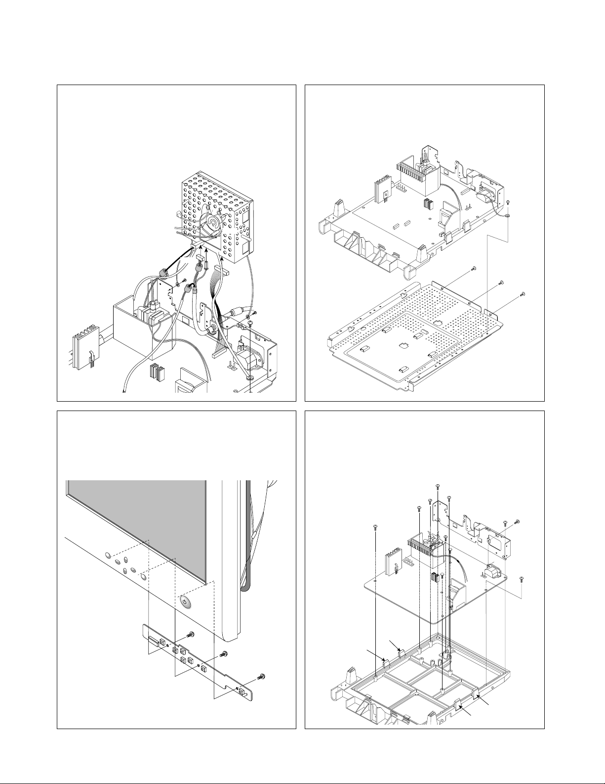
DISASSEMBLY
- 10 -
2. BACK COVER REMOVAL
1) Remove two screws cap (a).
2) Remove four screws (b) from the Back Cover.
3) Slide the Back Cover away from the Front
Cabinet of the monitor.
(a)
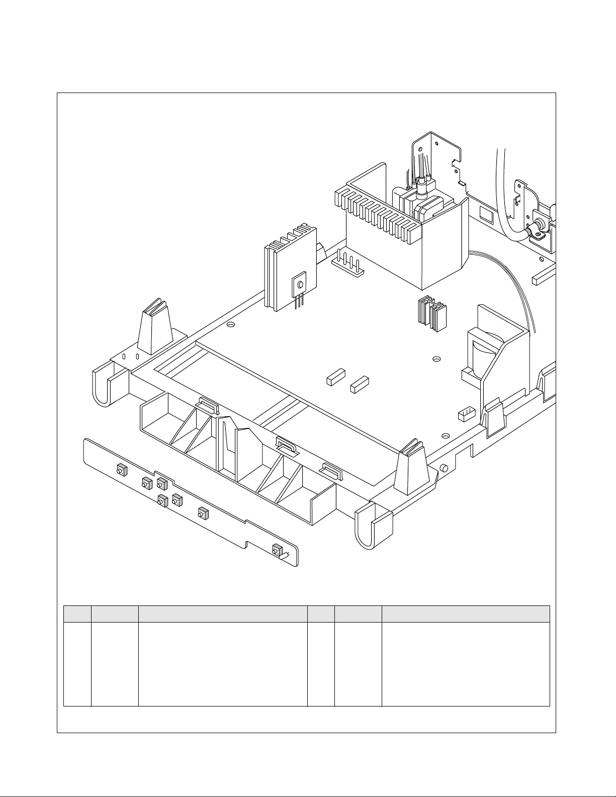
1. TILT/SWIVEL REMOVAL
1) Set the monitor face downward.
2) Pressing the latch (a), carefully remove
the Tilt/Swivel by pulling it upward.
(b)
(a)
(a)
(b)
P503
P703
P701
DY Assembly Screw
Control PCB
(P201)
Purity Coil
P902
(b)
(a)
(a)
(b)
SET
3. TOTAL CHASSIS ASSEMBLY
REMOVAL
1) Disconnect P903,P902(Degaussing pin),
P703(DY pin), P503(Tilt pin),
P502(Purity pin), P401
and P701 from the Main PCB.
2) Disconnect Pin four
from the Video PCB.
3) Carefully separate the CDT
Board Assembly from
the CDT neck.
4) Discharge the remaining
static electricity by shorting
between the Anode Cap
and the CDT ground.
5) Disconnect the Anode Cap
from the CDT.
6) Remove two screws (a).
7) Remove two screws (b).
8) Remove the Total Chassis
Assembly from the Main Frame.
Page 5
- 11 -
4. VIDEO PCB ASSEMBLY REMOVAL
1) Remove five screws (a).
2) Disconnect P301, P302, P303, and Pin (b).
3) Remove the Video PCB Assembly.
5. CONTROL PCB ASSEMBLY REMOVAL
1) Remove three screws (a).
2) Remove the Control PCB Assembly
from the Front Cabinet.
(a)
(a)
(a)
OSD SET
6. BOTTOM BRACKET REMOVAL
1) Remove four screws (a).
2) Remove the Bottom Bracket.
7. MAIN BRACKET REMOVAL
1) Remove three screws (a).
2) Remove the Rear Bracket.
3) Remove eight screws (b).
4) Release four latches (c),
and remove
the Bottom Bracket.
(a)
(a)
(a)
(a)
(a)
(a)
(b)
(b)
(c)
(c)
(c)
(c)
(b)
(b)
(b)
(b)
(b)
(b)
(a)
P301
(b)
(a)
P303
P302
(a)
(a)
Page 6

ADJUSTMENT
- 14 -
GENERAL INFORMATION
All adjustment are thoroughly checked and corrected
when the monitor leaves the factory, but sometimes
several adjustments may be required.
Adjustment should be following procedure and after
warming up for a minimum of 30 minutes.
• Alignment appliances and tools.
- IBM compatible PC.
- Programmable Signal Generator.
(eg. VG-819 made by Astrodesign Co.)
- EPROM or EEPROM with saved each mode data.
- Alignment Adaptor and Software.
- Digital Voltmeter.
- White Balance Meter.
- Luminance Meter.
- High-voltage Meter.
AUTOMATIC AND MANUAL DEGAUSSING
The degaussing coil is mounted around the CDT so that
automatic degaussing when turn on the monitor. But a
monitor is moved or faced in a different direction, become
poor color purity cause of CDT magnetized, then
press
DEGAUSS on the OSD menu.
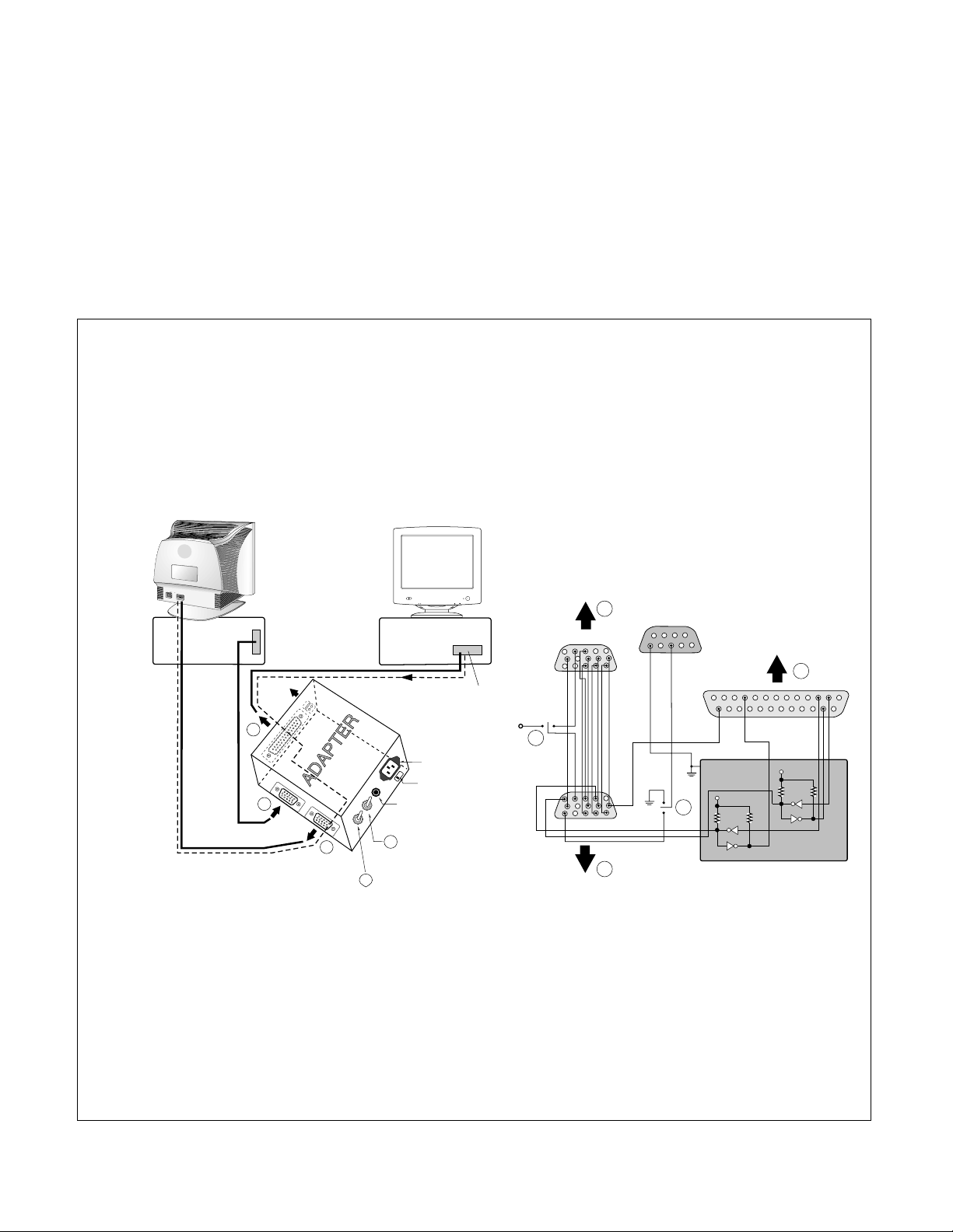
ADJUSTMENT PROCEDURE & METHOD
-Install the cable for adjustment such as Figure 1and run
the alignment program on the DOS for IBM compatible PC.
-Set external Brightness and Contrast volume to max position.
1. Adjustment for High-Voltage.
1) Display cross hatch pattern at Mode 8.
2) Adjust Anode voltage to 26kV
+
0.1kV.
2. Adjustment for Factory Mode (Preset Mode).
1) Display cross hatch pattern at Mode 8.
2) Run alignment program for FS772C on the
IBM compatible PC.
3) EEPROM→ALL CLEAR→Y(YES) command.
※ <Caution> Do not run this procedure unless the
EEPROM is changed.
All data in EEPROM (mode data and color data)will
be erased.
4) Power button of the monitor turn off → turn on.
5) COMMAND → START → Y(Yes) command.
6) DIST. ADJ. → TILT command.
7) Adjust tilt as arrow keys to be the best condition
8) DIST. ADJ. → BALANCE command.
9)
Adjust parallelogram as arrow keys to be the best
condition.
10)DIST. ADJ. → BALANCE command.
11) Adjust balance of side-pincushion as arrow keys to
be the best condition.
12)
DIST. ADJ. → FOS. ADJ command.
13)
Adjust V-SIZE as arrow keys to 230±2mm.
14)
Adjust V-POSITION as arrow keys to center of the
screen.
15)
Adjust H-SIZE as arrow keys to 310±2mm.
16)
Adjust H-POSITION as arrow keys to center of the
screen.
17)
Adjust S-PCC (Side-Pincushion) as arrow keys to be
the best condition.
18)
Adjust TRAPEZOID as arrow keys to be the best
condition.
19)
PRESET EXIT → Y (Yes) command.
3. Adjustment for White Balance and Luminance.
1) Set the White Balance Meter.
2)
Press the DEGAUSS on the OSD menu for demagnetization
of the CDT.
3) Set Brightness max and SUB-Brightness to 130(82)
(Decimal) position.
4) Display color 0,0 pattern at Mode 8.
5) COLOR ADJ. → LUMINANCE command of the
alignment program.
6) COLOR ADJ. → BIAS ADJ. command of the
alignment program.
7) Check whether R-BIAS and B-BIAS to min position
and G-BIAS to 0.7±0.05FL of the raster luminance.
Check it's not green color.
8) Adjust R-BIAS and B-BIAS command to x=0.283
±
0.02 and y=0.298±0.02 on the White Balance Meter
with PC arrow keys.
9) Adjust SUB-Brightness command to 0.5
±
0.1FL of the
raster luminance.
10)
Display color 15,0 window pattern (70x70mm) at Mode 8.
11)
Set Contrast max and SUB-Contrast to 127(7F)
(decimal) position.
12)
DRIVE ADJ command.
13)
Set G-DRIVE to 170(AA) (decimal) at DRIVE of the
alignment program.
14)
Adjust R-DRIVE and B-DRIVE command to white
balance x=0.283
±
0.02 and y=0.298±0.02 on the
White Balance Meter with PC arrow keys.
15)
Adjust SUB-CONTRAST command to 52±1FL of the
raster luminance at the save in color 1.
Page 7
- 15 -
Figure 1. Cable Connection
220
IBM
Compatible PC
PARALLEL PORT
Power inlet (required)
Power LED
ST Switch
Power Select Switch
(110V/220V)
Control Line
Not used
RS232C
PARALLEL
V-SYNC
POWER
ST
VGS
MONITOR
E
V-Sync On/Off Switch
(Switch must be ON.)
F
A
B
C
E
F
A
B
C
15
10
5
5
69
1
1
1
14
13
25
6
5V
5V
5V
4.7K
4.7K
4.7K
74LS06
74LS06
OFF ON
OFF
ON
11
VIDEO
SIGNAL
GENERATOR
16)
Display color 15,0 full white patten at Mode 8.
17)
COLOR ADJ. → LUMINANCE → ABL command.
18)
Adjust ABL to 34±1FL of the luminance.
19)
Exit from the program.
4. Adjustment for Focus.
1) Display “mE” character in full screen at Mode 8.
2) Adjust two Focus control on the FBT that focus
should be the best condition.
Monitor to be
adjusted
Page 8

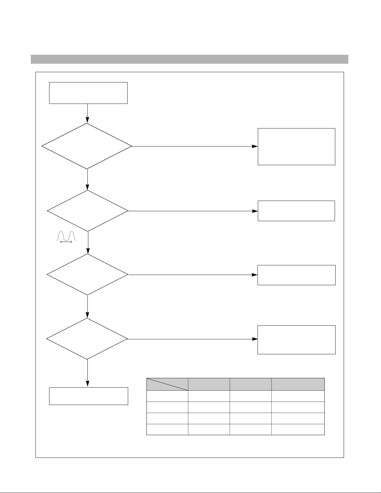
TROUBLESHOOTING GUIDE
- 16 -
NO POWER
(POWER INDICATOR OFF)
TROUBLE IN
D901
TROUBLE IN FUSE
(F901)
TROUBLE IN
IC901
TROUBLE IN
D931, D961, D991,
D951, D941,D971
TROUBLE IN
IC901
CHECK
FUSE OK?
CHECK
C908 VOLTAGE?
(AC220V: 310VDC)
NO
YES
YES
YES
YES
NO
NO
NO
CHECK
IC901 PIN 3
WAVEFORM
(SQUARE WAVE
COMES OUT?)
CHECK
D931, D961, D991,
D951, D941,D971
VOLTAGE?
1. NO POWER
Page 9

- 17 -
2. NO CHARACTER
NO CHARACTER
CHECK
IC302 PIN 7, 15, 18,
21(8V) ?
CHECK
IC302 PIN 6, 8, 10 ?
CHECK
IC302 PIN 16, 19, 22 ?
CHECK
IC303
PIN 1, 2, 3 ?
CHECK
IC303 PIN 4 (80V)
8 (12V) ?
TROUBLE IN
P302 12V LINE, IC304
TROUBLE IN
PC SIGNAL,
P301 SIGNAL CABLE
TROUBLE IN
IC302
TROUBLE IN
P302 12V LINE/80V LINE
TROUBLE IN IC303
NO
YES
NO
NO
YES
YES
YES
YES
NO
NO
CHECK
R, G, B CATHODE
VOLTAGE?
TROUBLE IN
R338~R341,
R344, R345, L302~L304,
D307~D310, D312, D313
TROUBLE IN
CRT SOCKET
YES
NO
Page 10

- 18 -
NO VIDEO
(POWER INDICATOR ON)
CHECK
POWER INDICATOR
GREEN or ORANGE?
CHECK
D712 ANODE
(-120V)?
CHECK
G1VOLTAGE?
(-5~25V)
TROUBLE IN
D712
TROUBLE IN
D941, Q941, Q942 (6.3V)
TROUBLE IN
Q703, Q704
DPM MODE
(NO H and/or V SYNC)
ORANGE
NO
GREEN
YES
YES
NO
3. NO RASTER
Page 11

- 19 -
4. TROUBLE IN H-LINEARITY
UNBALANCED OF H-LIN.
CHECK
IC401
PIN 19, 20, 21,
22, 23, 24?
CHECK
Q714~Q716, Q735, Q737
Q711~Q713, Q739
Q710?
TROUBLE IN
IC401 (MICOM)
TROUBLE IN
Q714~Q716, Q735, Q737
Q711~Q713, Q739, Q710
TROUBLE IN
RL701
NO
NO
YES
YES
Cs SIGNAL TABLE
HORIZONTAL
FREQUENCY(fH)
66K ~ 73K
62K ~ 66K
57K ~ 62K
49K ~ 57K
46K ~ 49K
43K ~ 46K
36K ~ 43K
33K ~ 36K
30K ~ 33K
Cs0
H
H
H
H
L
L
L
L
L
Cs1
H
H
L
L
H
L
H
H
L
Cs2
H
L
H
L
H
H
H
H
L
Cs3
H
H
H
H
H
H
L
L
L
Cs4
H
H
H
H
H
H
H
L
L
Page 12

- 20 -
5. NO VERTICAL DEFLECTION
NO V-DEFLECTION
(ONE HORIZONTAL LINE)
CHECK
IC601 PIN 2
(15V)?
CHECK
IC601 PIN 4
(-12V)?
CHECK
IC601 PIN 1 ?
TROUBLE IN
Q951, Q952, D951
15V LINE
TROUBLE IN
SMPS, D991
TROUBLE IN
IC701
TROUBLE IN
IC601, V-CIRCUIT
NO
NO
YES
YES
YES
NO
Page 13

- 21 -
TROUBLE IN
OSD PERIPHERAL
CIRCUIT
NO OSD
TROUBLE IN
5V LINE
TROUBLE IN
IC601 PIN6 (V-FBP),
T701 40V LINE
TROUBLE IN
IC302, IC301
TROUBLE IN
IC301, IC302
NO
YES
DC 5V
YES
YES
YES
NO
NO
NO
Pin 5
5V
Pin 10
5V
H+V
5V
H+V
CHECK
IC301 B
+
?
CHECK
IC301 PIN 12
WAVEFORM ?
(ENTER BUTTON MUST BE PRESSED.)
6. TROUBLE IN OSD
CHECK
IC301 PIN 5, 10
WAVEFORM?
CHECK
IC301 PIN 13, 14, 15 ?
Page 14
- 22 -
CHECK
IC401 (MICOM)
PIN 1, 42 (H/V INPUT)
SIGNAL?
CHECK
IC401 PIN 6
WAVEFORM?
CHECK
IC401 (MICOM)
PIN 3, 4 ?
CHECK
B+LINE
(6.3V,15V) ?
CHECK PC,
(PC IS NOT GOING INTO
DPM OFF MODE)
TROUBLE IN
X401
TROUBLE IN
IC401 (MICOM)
TROUBLE IN
Q941, Q942, Q951, Q952
TROUBLE IN PC
OFF MODE FAILURE
INPUT H/V SYNC SIGNAL
NO H/V SYNC
(NO OFF MODE.)
NO
NO
NO (DPMF: 0V)
DPM TABLE
Mode
Item
NORMAL
STAND-BY
SUSPEND
OFF
DPMS
H
L
L
L
LED
GREEN
AMBER
AMBER
AMBER
DPMF
H
H
H
L
YES
SEE DPM TABLE
YES
YES
5V
6MHz
7. TROUBLE IN DPM
Page 15

- 23 -
CHECK
IC401 PIN 31
(0V)?
CHECK
Q920 COLLECTOR
(15V)VOLTAGE?
CHECK
P902, P905?
CHECK
RL901?
TROUBLE IN
IC401 (MICOM)
TROUBLE IN
Q921
TROUBLE IN
P902, P905
TROUBLE IN
RL901
TROUBLE IN
TH901,
DEGAUSSING COIL
NO DEGAUSSING
DC 5V
NO
NO
NO
NO
YES
YES
YES
YES
(DEGAUSS ON THE OSD MENU MUST BE PRESSED.)
8. NO DEGAUSSING
Page 16

- 24 -
9. NO TILT (NO ROTATION)
NO TILT (NO ROTATION)
TROUBLE IN
IC401 (
MICOM)
TROUBLE IN
15V LINE, 6.3V LINE
TROUBLE IN
Q501~Q503
TROUBLE IN
P503, TILT COIL
NO
YES
YES
YES
CHECK
15V LINE
AND 6.3V LINE ?
CHECK
Q503 EMITTER
VOLTAGE ?
NO
NO
CHECK
Q504
WAVE FORM ?
Page 17

BLOCK DIAGRAM
- 12 -
POWER INPUT
200~240VA
C
(50Hz)
Line
Filter
Degaussing
Circuit
[ OSD Control ]
SMPS
CONTROL
(IC901)
120V
80V
50V
TILT
Control
Circuit
6.3V
15V
E
2
PROM
(IC402)
5V
OSD IC
(IC301)
H-Sync Sig
V-Sync Sig
I
2
C DATA(SDA )
I
2
C CLOCK(SCL)
VIDEO
PRE-AMP
(IC302)
Signal
Cable
RGB
VIDEO
MAIN AMP
(IC303)
8V REG.
(IC304)
8V
-12V
12V
CUT OFF
CONTROL
120V
12V
5V
H/V Sync P rocessor
( IC701 )
TDA9112
V-OUT
( IC601)
TDA8172
H-OUT
( Q706)
H-Linearity
Correction
DC/DC Converter
X-RAY
Protection
Circuit
Dynamic
Focus
Circuit
Auto
Beam
Limit
Vertical Blanking,
Brightness Control
- 120V
40V
15V
D/D Feed Back
30V
12V
MICOM
(IC401)
SCL / SDA
H/V Sync,
PWM Control
Sig
12V
15V
50V
DY CDT
Heater ( 6.3V )
I
2
C
I
2
C
I
2
C
H/V
Sync
Screen
Dynamic Focus
Static Focus
H.V
R/G/B
Bias
R/G/B
Contrast
H-DRV
B-DRV
B+
15V
TILT
COIL
DEGAUSSING
CO
REACTOR
IL
I
2
C
BRIGHTNESS/CO
NTRAST
COLOR CURVE
H / V POSITION
H / V SIZE
SPCC
TRAPIZODE
PIN BALANCE
PA RALLELOGRAM
ROTA TION
TOP CORNRE
BOTTOM CORMOR
RECALL
DEGAUSSING
MOIRE
PURITY
LANGUAGE
RECALL
DPM
CONTROL
CIRCUIT
850V
FBT
( T701 )
15V
SMPS
TRANS
(T901)
G
1
G
2
15V
IC992
12V REG.
6.3V
-12V
15V
12V 80V
12V
Voltage
feedback
Voltage
feedback
PURITY
Control
Circuit
PURITY
COIL
15V
6.3V
Page 18

DESCRIPTION OF BLOCK DIAGRAM
- 13 -
1. SMPS(Switching Mode Power Supply)
When you turn on the power switch, the operating
procedure is as follows:
1) The AC line voltage is rectified by the bridge diodes
D901 and C908
2) The control IC(IC901) starts switching and generates
switching pulses in the primary turns of the SMPS
transformer (T901)
3) The switching pulses of the primary turns are induced the
secondary turns of the transformer by the turn ratio.
These pulses are rectified by each diode (D971,D961,
D951, D931, D941 ,D991)
4) Each rectified DC voltage (120V, 50V, 15V, 80V, 6.3V,12V and 5V) is supplied to the main circuit.
2. Over Voltage Protection Circuit
When the input voltage of IC901 Vin(pin 4) is more than
22.5V(typical), all the secondary Voltages of the SMPS
transformer (T901) down to low value.
3. Display Power Management Circuit
1) Stand-by and Suspend mode.
When no input of horizontal or vertical sync, Q951 and
Q952 are turned off.
Then input power consumption is below 15 watts
2) OFF mode
When no input of horizontal and vertical sync,
Then input power consumption is below 5 watts
4. X-ray Protection Circuit
If the high voltage of the FBT reaches up to 29KV IN an
abnormal case, Q807 operates and IC401 pin 41 came
to low level, Then IC401 control IC701 to stop Horizontal
drive pulse and stop Horizontal Deflection.
5. Microprocessor Control Circuit.
1) Horizontal and Vertical sync signals are supplied to the
microprocessor (IC401).
2) Microprocessor(IC401) discriminates the operating mode
from the sync polarity and resolution.
3) After microprocessor reads these adjusted mode data
stored at EEPROM, it controls operating mode data
through IIC
4)
Users can control screen condition by the OSD, SET, UP,
DOWN, RIGHT, LEFT, and Audio and Audio Mute buttons.
6. D/D Convert Circuit.
To obtain constant high voltage, this circuit supplies
controlled DC voltage for FBT and Horizontal deflection
circuit according to the horizontal sync frequency.
7. Horizontal and Vertical Sync Processor Circuit.
The horizontal and vertical sync processor IC (IC701)
has a sync detector, a saw-tooth generator, and drive
function. So output horizontal and vertical drive signal
control screen distortions.
8. Horizontal linearity Circuit.
This circuit corrects the horizontal linearity for each
horizontal sync frequency.
9. Horizontal drive and Output Circuit.
This circuit is a horizontal deflection amplifier for raster
scan.
10. ABL Circuit.
This circuit limits the beam-current for the reliability of the
CDT.
11. Vertical Output Circuit.
This circuit takes the vertical ramp wave from the
TDA9112(IC701) and performs the vertical deflection by
supplying the saw-tooth wave current to the vertical
deflection yoke.
12. Blanking and Brightness Control Circuit.
Blanking circuit eliminates the retrace line by supplying a
negative pulse wave to the G1 of the CDT.
Brightness control circuit is used for control of the screen
brightness by changing the DC level of the G1.
13. Video Processor Circuit.
Video processor circuit consists of the video drive output
block. The video drive IC(IC302) receives the video
signal from PC. The gain of each channel is controlled by
the voltage of contrast pin. The cut-off circuit compensate
different voltage of each channel between the cathode
and the G1 of the CDT.
14. OSD (On-Screen-Display) Circuit.
This circuit displays on the screen information of the
monitor’s status.
15. Dynamic Focus Output Circuit.
This circuit takes the horizontal and the vertical parabola
waves from the TDA9112(IC701) and amplifies it to
maintain constant focus on center and comers in the
screen.
17. Image Rotation (Tilt) Circuit.
This circuit corrects the tilt of the screen by supplying the
image rotation signal to the tilt coil which is attached near
the deflection yoke of the CRT.
18. Earth Margnetic Correction(Purity) Circuit
This circuit corrects the convergence of screen by
suppling the convergence signal to the coil which is
attached to the CRT near the deflection.
Page 19

WIRING DIAGRAM
- 9 -
P503
P703
P701
P902
DY Assembly Screw
Page 20

3.11V
0.5V
42.8V
45V
4.5V
-7V
4.5V
19.1V
0.4
51.2V
11.4ms
340V
130V
60V
17.8V
12V
247
400 210
14.6V
-2.0V
1098V
14.54
1.3~1.94V
Page 21

EXPLODED VIEW
1
2
4
6
9
10
15
11
12
7
3
B
A
C
13-2
14-1
14-2
13-1
OSD SET
5
8
EXPLODED VIEW PARTS LIST
Ref. No.
1
2
3
4
5
6
7
8
9
10
11
12
13-1
13-2
14-1
14-2
15
A
B
C
Part No.
3091TKC040B
2423GC3E41M
339-002D
6140TC2007D
6174Z-1044A
6620TKB002A
6871TST225B
4950TKK171B
4810TKM037L
332-102G
4814TKK077B
3809TKC034E
3550TKK061L
3550TKK061M
332-102P
332-102J
3043TKK040U
6871TMT225B
6871TVT225B
3313T17226B
Description
CABINET ASSY FS772C FUJITSU SIMENS 039
CDT SET, M41QBF423X 31NPLD
SCREW ASSY, PHP+5*30BP(FZMY)+GW18 #(4)CDT FIX
COIL,DEGAUSSING, 1410MM 18.5OHM 0.45MM 120T 17" 220V, PURITY
FBT (FLY BACK TRANSFORMER), FMMTC91 M1044A (LIM SANG IL)
SOCKET (CIRC),POWER, BCP-03A-3 BAE EUN AC UNIVERSAL 3PIN BLACK
PWB(PCB) ASSY,SUB FS772C KZFSED FUJITSU SIMENS CA-87 LGEDI TOTAL
METAL REAR KFB775B
BRACKET, KFB775C MAIN J-CKD
SCREW, PTP 4*30 FZMW
SHIELDBOTTOM KFB775B
BACK COVER ASSY, FS772C 016 F-SIEMENS
COVER FS772C SCREW F-SIEMENS (RIGHT)
COVER FS772C SCREW F-SIEMENS (LEFT)
SCREW, PTP 4*30[MSWR/FZMCWY-1] #C/A+B/C (UP)
SCREW, PTP 4*20 (FZMW) #C/A+B/C (DOWN)
TILT SWIVEL ASSY, FS772C T032B029B F-SIEMENS
PWB(PCB) ASSY,MAIN FS772C KZFSED FUJITSU SIMENS CA-87 LGEDI TOTAL
PWB(PCB) ASSY,VIDEO FS772C KZFSED FUJITSU SIMENS CA-87 LGEDI TOTAL
MAIN TOTAL ASSY, FS772C FUJITSU SIMENS CA-87 LGEDI
 Loading...