

Page 1

series
USER'S MANUAL
PULSE TRAIN POSITIONING CONTROL
COMBINED MODULE
FEH214a
Page 2

Preface
This User’s Manual explains the pulse train positioning control combined module. Read this manual carefully to ensure
correct operation.
When using modules or peripheral devices, be sure to read the corresponding user’s manuals listed below.
eltiT .oNlaunaM stnetnoC
XS-XERCIM,noitcurtsnIlaunaMs'resU
HPSseires
XS-XERCIM,erawdraHlaunaMs'resU
HPSseires
,>noitcudortnI<niw003DlaunaMs'resU
seiresXS-XERCIM
,>ecnerefeR<niw003DlaunaMs'resU
seiresXS-XERCIM
dnammocgolanAlaunaMs'resU
,eludomdenibmoclortnocgninoitisop
HPSseiresXS-XERCIM
tuptuoniartesluPlaunaMs'resU
XS-XERCIM,eludomlortnocgninoitisop
HPSseires
002HEF ehtfosnoitinifedmetsysdnaegaugnal,yromemehtsnialpxE
.seiresXS-XERCIM
102HEFdnasnoitacificepseht,noitarugifnocmetsysehtsnialpxE
.seiresXS-XERCIMehtniseludomfosnoitarepo
052HEFgnimmargorpeht,niw003DfosnoitarepocisabehtsnialpxE
.seiresXS-XERCIMrofgnirotinomdna
452HEFehtfolladnaniw003DfonocidnaunemehtsnialpxE
.niw003Dfosnoitarepo
312EHF gninoitisopdnammocgolanaehtfosnoitarepoehtsnialpxE
.eludomdenibmoclortnoc
512HEF gninoitisoptuptuoniarteslupehtfosnoitarepoehtsnialpxE
.eludomlortnoc
The following product is being developed.
NP1F-MP1
Notes
1. This manual may not be reproduced in whole or part in any form without prior written approval by the manufacturer.
2. The contents of this manual (including specifications) are subject to change without prior notice.
3. If you find any ambiguous or incorrect descriptions in this manual, please write them down (along with the manual
No. shown on the cover) and contact FUJI.
Page 3

Be sure to read the “Safety Precautions” thoroughly before using the module.
Here, the safety precaution items are classified into “Warning” and “Caution.”
Safety Precautions
Warning
Caution
Even some items indicated by “Caution” may also result in a serious accident.
Both safety instruction categories provide important information. Be sure to strictly observe these instructions.
: Incorrect handling of the device may result in death or serious injury.
: Incorrect handling of the device may result in minor injury or physical damage.
Warning
◊ Never touch any part of charged circuits as terminals and exposed metal portion while the power is turned ON. It may
result in an electric shock to theoperator.
◊ Turn OFF the power before mounting, dismounting, wiring, maintaining or checking, otherwise, electric shock, erratic
operation or troubles might occur.
◊ Place the emergency stop circuit, interlock circuit or the like for safety outside the PC. A failure of PC might break or
cause problems to the machine.
◊ Do not connect in reverse polarity, charge (except rechargeable ones), disassemble, heat, throw in fire or short-circuit
the batteries, otherwise, they might burst or take fire.
◊ If batteries have any deformation, spilled fluids, or other abnormality, do not use them. The use of such batteries might
cause explosion or firing.
◊ Do not open the FG terminal with the LG-FG short circuited. (It must be grounded, otherwise it might cause electric
shock.)
Page 4

Safety Precautions
Caution
◊ Do not use one found damaged or deformed when unpacked, otherwise, failure or erratic operation might be caused.
◊ Do not shock the product by dropping or tipping it over, otherwise, it might be damaged or troubled.
◊ Follow the directions of the operating instructions when mounting the product. If mounting is improper, the product
might drop or develop problems or erratic operations.
◊ Use the rated voltage and current mentioned in the operating instructions and manual. Use beyond the rated values
might cause fire, erratic operation or failure.
◊ Operate (keep) in the environment specified in the operating instructions and manual. High temperature, high humidity,
condensation, dust, corrosive gases, oil, organic solvents, excessive vibration or shock might cause electric shock, fire,
erratic operation or failure.
◊ Select a wire size to suit the applied voltage and carrying current. Tighten the wire terminals to the specified torque.
Inappropriate wiring or tightening might cause fire, malfunction, failure, or might cause the product to drop from its
mounting.
◊ Contaminants, wiring chips, iron powder or other foreign matter must not enter the device when installing it, otherwise,
erratic operation or failure might occur.
◊ Remove the dust-cover seals of modules after wiring, otherwise, fire, accidents, failure or fault might occur.
◊ Connect the ground terminal to the ground, otherwise, an erratic operation might occur.
◊ Periodically make sure the terminal screws and mounting screws are securely tightened.
Operation at a loosened status might cause fire or erratic operation.
◊ Put the furnished connector covers on unused connectors, otherwise, failure or erratic operation might occur.
◊ Install the furnished terminal cover on the terminal block, otherwise, electric shock or fire might occur.
◊ Sufficiently make sure of safety before program change, forced output, starting, stopping or anything else during a run.
The wrong operation might break or cause machine problems.
◊ Engage the loader connector in a correct orientation, otherwise, an erratic operation might occur.
◊ Before touching the PC, discharge any static electricity that may have been collected on your body. To discharge it,
touch a grounded metallic object. Static electricity might cause erratic operation or failure of the module.
◊ Be sure to install the electrical wiring correctly and securely, observing the operating instructions and manual. Wrong or
loose wiring might cause fire, accidents, or failure.
◊ When disengaging the plug from the outlet, do not pull the cord, otherwiase, break of cable might cause fire or failure.
◊ Do not attempt to change system configurations (such as installing or removing I/O modules) while the power is ON,
otherwise, failure or erratic operation might occur.
◊ Do not attemp to repair the module by yourself contact your Fuji Electric agent. When replacing the batteries, correctly
and securely connect the battery connectors, otherwise, fire, accidents or failure might occure.
◊ To clean the module, turn power off and wipe the module with a cloth moistened with warm water. Do not use thinner or
other organic solvents, as the module surface might become deformed or discolored.
◊ Do not remodel or disassemble the product, otherwise, a failure might occur.
◊ Follow the regulations of industrial wastes when the device is to be discarded.
◊ The modules covered in these operating instructions have not been designed or manufactured for use in equipment or
systems which, in the event of failure, can lead to loss of human life.
◊ If you intend to use the modules covered in these operating instructions for special applications, such as for nuclear
energy control, aerospace, medical, or transportation, please consult your Fuji Electric agent.
◊ Be sure to provide protective measures when using the module covered in these operating instructions in equipment
which, in the event of failure, may lead to loss of human life or other grave results.
◊ External power supply (such as 24V DC power supply) which is connected to DC I/O should be strongly isolated from
AC power supply.
Page 5

nodetnirP .oNlaunaM* stnetnocnoisiveR
8991.peS412HEFnoitidetsriF
2002.naJa412HEFdenifeR
Revision
.revocehtnonwohssi.oNlaunaM*
Page 6

Contents
Preface
Safety Precautions
Revision
Contents
page
Section 1 General ......................................................................................... 1-1
1-1 Precautions..................................................................................................................................... 1-1
1-2 Functional Overview ...................................................................................................................... 1-2
1-2-1 Overview of NP1F-MP1/NP1F-MP2 functions....................................................................................... 1-2
1-2-2 Overview of NP2F-LEV functions .......................................................................................................... 1-3
Section 2 System Configuration ..................................................................2-1
2-1 Configuration of Peripheral Equipment....................................................................................... 2-1
2-2 Applied System .............................................................................................................................. 2-2
2-2-1 Appli c a ble C P U ...................................................................................................................................... 2-2
2-2-2 Applied system configuration................................................................................................................. 2-2
2-3 Loader and Software Modules to be Used .................................................................................. 2-3
Section 3 Specifications ...............................................................................3-1
3-1 General Specifications (NP1F-MP1/NP1F-MP2) ........................................................................... 3-1
3-1-1 General specifications (NP2F-LEV)....................................................................................................... 3-2
3-2 Specifications (NP1F-MP1/NP1F-MP2).........................................................................................3-3
3-2-1 Specifications (NP2F-LEV) .................................................................................................................... 3-3
3-3 Names.............................................................................................................................................. 3-4
3-3-1 NP1F-MP1 (for 1 axis) ........................................................................................................................... 3-4
3-3-2 NP1F-MP2 (for 2 axes) .......................................................................................................................... 3-6
3-3-3 NP2F-LEV (Signal converter) ................................................................................................................ 3-8
3-4 Dimensions ................................................................................................................................... 3-10
3-4-1 NP1F-MP1 (for 1 axis) ......................................................................................................................... 3-10
3-4-2 NP1F-MP2 (for 2 axes) ........................................................................................................................ 3-10
3-4-3 NP2F-LEV (Signal converter) .............................................................................................................. 3-11
Section 4 Wiring.............................................................................................4-1
4-1 Mounting Precautions.................................................................................................................... 4-1
4-1-1 Number of mountable modules (NP1F-MP1/ NP1F-MP2) .................................................................... 4-1
4-1-2 Wiring precautions ................................................................................................................................. 4-2
4-1-3 Wiring example of the external wiring connector................................................................................... 4-2
4-2 Connector Pin Layout for the External Connection (NP1F-MP1) .............................................. 4-3
4-2-1 External I/O signal specifications (NP1F-MP1) ..................................................................................... 4-4
4-2-2 External I/O signal interface (NP1F-MP1) ............................................................................................. 4-5
4-3 Connector Pin Layout for the External Connection (NP1F-MP2) .............................................. 4-9
4-3-1 External I/O signal specifications (NP1F-MP2) ................................................................................... 4-10
4-3-2 External I/O signal interface (NP1F-MP2) ........................................................................................... 4-11
4-4 Connector Pin Layout for the External Connection (Signal Converter) ................................. 4-17
4-4-1 External I/O signal specifications (Signal converter)........................................................................... 4-18
4-4-2 External I/O signal interface (Signal converter)................................................................................... 4-19
Page 7

Contents
page
4-5 Connecting..................................................................................................................................... 4-21
4-5-1 Connecting sample of a servo motor................................................................................................... 4-21
4-6 I/O Wiring....................................................................................................................................... 4-24
Section 5 Memory Map .................................................................................5-1
5-1 NP1F-MP1/NP1F-MP2 Memory Map (Internal Memory List)....................................................... 5-1
5-2 NP1F-MP1 I/O Area......................................................................................................................... 5-2
5-2-1 NP1F-MP1 (read area: address No. 0 to No. 9)..................................................................................... 5-3
5-2-2 NP1F-MP1 (Write area: address Nos. 10 to 13).................................................................................. 5-18
5-3 I/O Area of NP1F-MP2 .................................................................................................................. 5-35
5-3-1 NP1F-MP2 (Read area: address No. 0 to No. 13) ............................................................................... 5-36
5-3-2 NP1F-MP2 (Write area: address Nos. 14 to 21).................................................................................. 5-67
5-4 Setting Method and Effective Bits of Individual Register........................................................ 5-99
Section 6 Parameter s (Registers) ................................................................6-1
6-1 Parameters List (Registers)........................................................................................................... 6-1
6-2 Relationship between Parameters (Registers)............................................................................ 6-2
6-3 Detailed Description of Parameters (Registers) ......................................................................... 6-4
Section 7 Positioning Function....................................................................7-1
7-1 Positioning Function of the Pulse Train Positioning Control Combined Module
(NP1F-MP1/NP1F-MP2) .................................................................................................................. 7-1
7-2 Functions of Each Operation Mode.............................................................................................. 7-3
7-3 Functions of Pulse Generation Mode .......................................................................................... 7-4
7-3-1 Positional deviation calculation function................................................................................................ 7-5
7-3-2 Command pulse count control ............................................................................................................... 7-6
7-3-3 Command pulse frequency control ........................................................................................................ 7-7
7-3-4 Trapezoidal acceleration/deceleration ................................................................................................... 7-8
7-3-5 Automatic deceleration point calculation ............................................................................................. 7-10
7-3-6 Deceleration point setting .................................................................................................................... 7-11
7-3-7 Continuous frequency rewriting ........................................................................................................... 7-12
7-3-8 Setti n g d a t a t o a r e g i s t e r ...................................................................................................................... 7-13
7-3-9 Data reading from register ................................................................................................................... 7-14
7-3-10 Current value data reading ................................................................................................................ 7-15
7-3-11 Manual operation ............................................................................................................................... 7-16
7-3-12 Ori g i n a l p o i n t r e t u rn motio n ............................................................................................................... 7-17
7-3-13 Positioning operation.......................................................................................................................... 7-18
7-3-14 Inte r rupt point p o s i t i o n i n g m o t i o n ...................................................................................................... 7-19
7-3-15 Dece l e r a t i o n - a n d - s t o p / q u i ck st o p m o t i o n ........................................................................................ 7-20
7-3-16 Operation when an emergency stop error has been detected.......................................................... 7-21
7-3-17 Operation when an ±OT error has been detected............................................................................. 7-22
7-3-18 Command pulse counting .................................................................................................................. 7-24
7-3-19 Operation when a transmission error has been detected ................................................................. 7-25
7-3-20 Positioning using the FIFO buffer ...................................................................................................... 7-26
7-3-21 Setting the data to be added to the command pulse register while speed is continuously
changed over..................................................................................................................................... 7-28
7-3-22 Backlash compensation ..................................................................................................................... 7-29
7-3-23 Feedback pulse multiplication............................................................................................................ 7-29
Page 8

Contents
page
7-4 Functions of the Position Command Mode............................................................................... 7-31
7-4-1 Positional deviation calculation ............................................................................................................ 7-32
7-4-2 Operation at the rising edge of start signal ......................................................................................... 7-33
7-4-3 Operation when start command is “ON” .............................................................................................. 7-33
7-4-4 Processing when start command is tur ned OFF .................................................................................7-35
7-4-5 Original point return motion ................................................................................................................. 7-35
7-4-6 Interrupt positioning ............................................................................................................................. 7-35
7-4-7 Operation when an emergency stop error has been detected............................................................ 7-36
7-4-8 Operation when an ± OT error has been detected.............................................................................. 7-36
7-4-9 Operation when a transmission error has been detected ................................................................... 7-36
7-4-10 Operation for resetting deviation........................................................................................................ 7-37
7-4-11 Backlash compensation ..................................................................................................................... 7-37
7-4-12 Feedback pulse multiplication............................................................................................................ 7-37
7-5 External Input Pulse Functions .................................................................................................. 7-39
7-5-1 External pulse c o u n t i n g ....................................................................................................................... 7-39
7-5-2 Detection time of this module .............................................................................................................. 7-40
Section 8 Troubleshooting............................................................................8-1
8-1 LED Indication ................................................................................................................................ 8-1
8-2 Error Indication............................................................................................................................... 8-2
Appendix...................................................................................................App.-1
Appendix-1 Parameters (Registers) .............................................................................................. App.-1
Appendix-2 The Relationship between Operation Mode and Parameter.................................. App.-2
Appendix-3 The Relationship between Operation Mode and Bit Data Signal.......................... App.-3
Appendix-4 Memory Map ............................................................................................................. App.-10
Appendix-5 Terminology.............................................................................................................. App.-12
Appendix-6 Current Consumption and Mass of Modules in MICREX-SX Series................... App.-14
Page 9

Section 1 General
Page
1-1 Precautions ................................................................................................................. 1-1
(1) Handling precautions as precision device...............................................................................................1-1
(2) Precautions concerning operating conditions and environment .............................................................1-1
1-2 Functional Overview...................................................................................................1-2
1-2-1 Overview of NP1F-MP1/NP1F-MP2 functions ...................................................................... 1-2
1-2-2 Overview of NP2F-LEV functions ......................................................................................... 1-3
Page 10

Section 1 General
1-1 Precautions
The NP1F-MP1/NP1F-MP2 is a pulse train positioning control combined module which is connected to a CPU module via
an SX bus. It is used in combination with a pulse train input command-type servo amplifier + motor or with a stepping
motor driver to perform high-accuracy positioning. When the separate differential conversion unit (NP2F-LEV) is used, it
can be connected to differential I/O devices.
Precautions for using the NP1F-MP1/NP1F-MP2 are as follows:
(1) Handling precautions as precision device
1) Do not drop the device.
2) Avoid installing the device in places subject to strong vibrations.
3) Avoid installing the device in places where harmful gas (corrosive gas) exists.
4) Avoid installing the device within the same panel as high-tension (3000V or 6000V or more) devices.
5) Avoid sharing the same power supply with equipment which produces high noise (e.g. inverter).
6) Avoid using the device in places where the temperature is too high or low, or the humidity is too high.
Operating ambient temperature: 0 to 55°C
Operating ambient humidity : 20 to 95%RH
7) In places with extremely low humidity, excessive static electricity tends to build up. When you touch the NP1F-
MP1/NP1F-MP2 in such an environment, be sure to touch a metal ground in advance in order to discharge the
static electricity which is charged on your body.
(2) Precautions concerning operating conditions and environment
When the NP1F-MP1/NP1F-MP2 is used in the following conditions or environment, secure enough margin for the rated
specifications and functions (performance), take sufficient fail-safe measures, and be sure to consult with personnel at
your Fuji Electric sales office.
1) Storage or use in conditions or an environment which is not described in the operating instructions or user's
manual
2) Applications in nuclear power generation control, railways, aircraft, railcars, incinerator equipment, medical
facilities, amusement machines, safety devices, etc.
3) Applications where a great effect on human life or proper ty may be anticipated and a high degree safety is
required
1-1
Page 11
1-2 Functional Overview
1-2-1 Overview of NP1F-MP1/NP1F-MP2 functions
metI noitpircseD
sexalortnocforebmuN)2PM-F1PN(2/)1PM-F1PN(1
epyttuptuO )eslupesrever+eslupdrawrof(tuptuoniartesluprotcellocnepO
ycneuqerfdnammoc.xaMzHk052
citsiretcarahcnoitareleced/noitareleccA )edomnoitarenegeslupni(noitareleced/noitareleccaladiozeparT
noitcerroCnoitcerrochsalkcaB
tniopnoitarelecedfonoitaluclaCnoitaluclaccitamotuA
)F/Ilaires(F/IedisUPC
)resluplaunam(tupniesluplanretxE
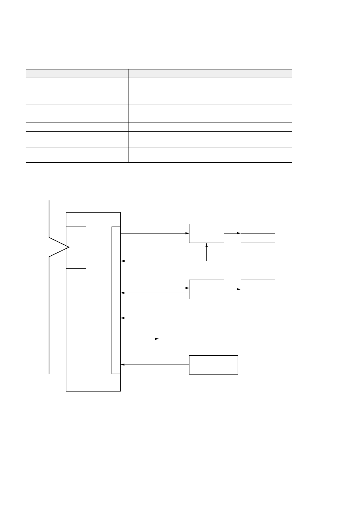
A sample connection configuration of the NP1F-MP1 is shown below:
Sample connection configuration of the NP1F-MP1
)sdrow41:latot,sdrow4:tuptuo,sdrow01:tupni(1PM-F1PN
)sdrow22:latot,sdrow8:tuptuo,sdrow41:tupni(2PM-F1PN
)detcennocebnacresluplaunam1(1PM-F1PN
)detcennocebnacresluplaunam1(2PM-F1PN
SX bus
NP1F-MP1
Serial
I/F
External I/Fs
X-axis forward/reverse
pulse
Feedback pulse
X-axis forward/reverse
pulse
Timing output
DI : X axis (EMG, ±OT, origin LS, interrupt (5 points))
DO: Command output from CPU module (2 points)
External pulse
Servo
amplifier
Stepping
driver
Manual
pulse generator
Motor
Encoder
Motor
1-2
Page 12
1-2-2 Overview of NP2F-LEV functions
metI noitpircseD
slennahcnoisrevnocforebmuN)sexa4rof(4
epyttupnI
ycneuqerftupnIzHM1.xaM
epyttuptuO)revirdenil(langislaitnereffiD
ycneuqerftuptuOzHM1.xaM
A sample connection configuration of the NP2F-LEV is shown below:
Sample connection configuration of the NP2F-LEV
)eslupesreverroeslup
1-2 Functional Overview
drawrof(tupniniartesluprotcellocnepO
SX bus
NP1F-MP2
Serial
I/F
External I/Fs
X-axis
forward pulse
X-axis
reverse pulse
Y-axis
forward pulse
Y-axis
reverse pulse
Feedback pulse
External pulse
NP2F-LEV
Motor
Servo
amplifier
Encoder
Motor
Servo
amplifier
Encoder
DI: X-/Y-axis (EMG, ±OT, origin LS, interrupt)
DO: Command output from CPU module (X-/Y-axis each 2 points)
Manual
pulse generator
1-3
Page 13
1-2 Functional Overview
A sample connection configuration of the NP2F-LEV and NP1F-MP1 is as follows:
Sample connection configuration of the NP2F-LEV
SX bus
NP1F-MP1
Serial
I/F
External I/Fs
X-axis
forward pulse
X-axis
reverse pulse
NP2F-LEV
Motor
Servo
amplifier
Encoder
NP2F-LEV
Feedback pulse
Phase-A
External pulse
Phase-B
Phase-Z
DI: X axis
(EMG, ±OT, origin LS, interrupt)
DO: Command output from CPU module (2 points)
Manual
pulse generator
1-4
Page 14

Section 2 System Configuration
Page
2-1 Configuration of Peripheral Equipment....................................................................2-1
2-2 Applied System ........................................................................................................... 2-2
2-2-1 Applicable CPU..................................................................................................................... 2-2
2-2-2 Applied system configuration ................................................................................................ 2-2
(1) For a 2-axis system.................................................................................................................................2-2
(2) Sample extensions (for 8-axis system) ...................................................................................................2-2
2-3 Loader and Software Modules to be Used ............................................................... 2-3
Page 15
Section 2 System Configuration
2-1 Configuration of Peripheral Equipment
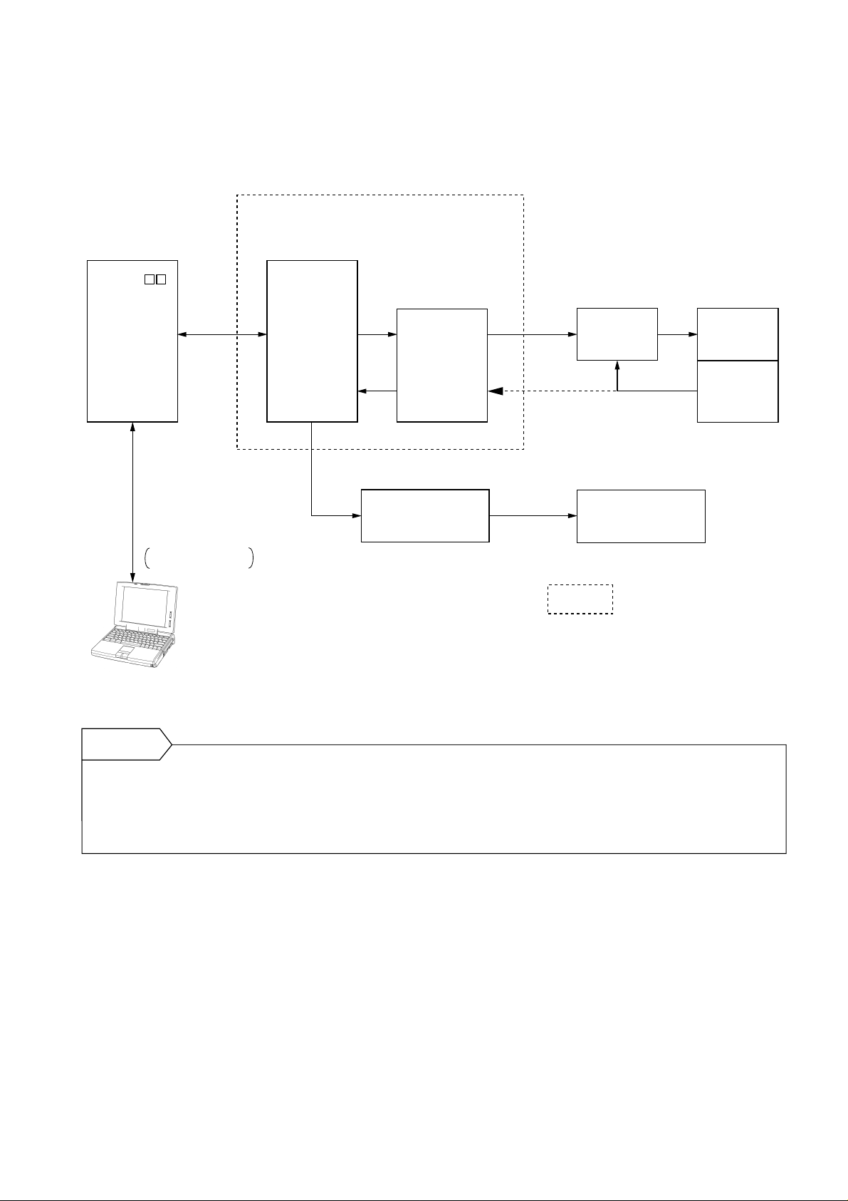
The overall configuration of the MICREX-SX series CPU and peripheral equipment is shown below:
Overall configuration
Positioning
CPU module
control module
NP1PS-
(Various-type
expansion
FBs for
positioning)
D300win
Positioning
loader software
General-purpose PC
SX bus
NP1F-MP1
NP1F-MP2
Signal converter
NP2F-LEV
Stepping
motor driver
Servo
amplifier
Stepping motor
: Area covered by this manual
Motor
Encoder
Precaution:
• This module only contains the basic functions for positioning processing.
Motion-related functions (manual motion, original point return motion, interpolation, etc.) are processed by the
expansion FB (function block) which is integrated into the MICREX-SX series high-performance CPU module.
• When fail-soft operation needs to be set, be sure to use “1030” or later version of the high-performance or standard
CPU module and “2030” or later version of the positioning module.
2-1
Page 16
2-2 Applied System
2-2-1 Applicable CPU
The NP1F-MP1/NP1F-MP2 can be used with a MICREX-SX series CPU.
1) High-performance CPU module ..... NP1PS-
2) Standard CPU module ..... NP1PH-
2-2-2 Applied system configuration
The NP1F-MP1/NP1F-MP2 is connected to the CPU module via an SX bus.
Sample connections are shown below:
(1) For a 2-axis system
Power supply module
CPU module
Input module
Positioning control module
(2 axes)
Output module
Power supply module : NP1S-22 (Double-slot type)
CPU module : NP1PSBase board : NP1BS-06
Positioning control module : NP1F-MP2
Input module : NP1X1606-W
Output module : NP1Y16T09P6
(2) Sample extensions (for 8-axis system)
Power supply module CPU module Positioning control module
Power supply module : NP1S-22 (Double-slot type)
CPU module : NP1PSBase board : NP1BS-06
Positioning control module : NP1F-MP2
Extension cable
Input module : NP1X1606-W
Output module : NP1Y16T09P6
Extension
cable
Positioning control
module
:
SX bus terminating plug
(NP8B-BP)
(2 axes)
(2 axes)
(2 axes)
Input module Output module
(2 axes)
For how to mount the modules, refer to Section 4.
:
NP1C-P3
2-2
Page 17

2-3 Loader and Software Modules to be Used
As shown in the above overall configuration, the following loader and software modules are necessary to operate the
NP1F-MP1/NP1F-MP2.
erawtfosredaoL epyT noitacilppA
gnimmargorpdetpadaniw003D
loottroppus
erawtfoS epyT noitacilppA
)BF(kcolbnoitcnufnoisnapxE
lortnocgninoitisoprofegakcap
)BF(kcolbnoitcnufnoisnapxE·
maccinortcelerofegakcap
)BF(kcolbnoitcnufnoisnapxE·
tucgninnurrofegakcap
DES-H4PNnoitacilpparotinom/etirw/daer/retsigeR
.UPCehtrofsmargorp
FPTP-N4PNsixatnednepednirofsmargorpnoitacilppA
launam,noitomdetalopretni,noitarepo
ebnacnrutertnioplanigirodnanoitarepo
.detceles
FMAC-N4PNlairetamgnikcapdoofroleetsdellortucotdesU
.seceiphtgnel-tesotni
2-3
Page 18

Section 3 Specifications
Page
3-1 General Specifications (NP1F-MP1/NP1F-MP2) ........................................................3-1
3-1-1 General specifications (NP2F-LEV) ...................................................................................... 3-2
3-2 Specifications (NP1F-MP1/NP1F-MP2)...................................................................... 3-3
3-2-1 Specifications (NP2F-LEV) ................................................................................................... 3-3
3-3 Names ..........................................................................................................................3-4
3-3-1 NP1F-MP1 (for 1 axis) .......................................................................................................... 3-4
3-3-2 NP1F-MP2 (for 2 axes) ......................................................................................................... 3-6
3-3-3 NP2F-LEV (Signal converter) ...............................................................................................3-8
3-4 Dimensions................................................................................................................ 3-10
3-4-1 NP1F-MP1 (for 1 axis) ........................................................................................................ 3-10
3-4-2 NP1F-MP2 (for 2 axes) ....................................................................................................... 3-10
3-4-3 NP2F-LEV (Signal converter) ............................................................................................. 3-11
Page 19

3-1 General Specifications (NP1F-MP1/NP1F-MP2)
metI noitacificepS
htgnertscirtceleiD )dnuorgemarfdnasniprotcennocO/Ineewteb(etunim1CAV0051
ecnatsisernoitalusnIm01 Ω )dnuorgemarfdnasniprotcennocO/Ineewteb(reggemCDV005htiweromro
tneibmagnitarepO
erutarepmet
erutarepmetegarotS
lacisyhP
latnemnorivne
snoitidnoc
lacinahceM
ecivres
snoitidnoc
lacirtcelE
ecivres
snoitidnoc
noitallatsnI
snoitidnoc
tsuD
noitarbiV
kcohS
dleif
ylppusrewoP
ylppus
gnilooCgniloocriA
ssaM
ytidimuhevitaleR
eergednoitulloP
ytinumminoisorroC
edutitlagnitarepO
erusserpcirehpsomtA
ytinummiesioN1htdiweslup,sn1emitesir,Vk1 µ )rotalumisesion(s
citatsortcelE
egrahcsid
citengamortceleoidaR
rewoPlanretxE
tnerruclanretnI
noitpmusnoc
noitcurtsnoC )epytdetnuomlenaP(epytkcolbgnidliuB:2PM-F1PN/1PM-F1PN
snoisnemiD
Section 3 Specifications
55ot0 ° C
07+ot52- ° C
noitasnednoconHR%59ot02
)noitasnednoconHR%59ot5:noitidnoctropsnarT(
tsudevitcudnocmorfeerF
2
.retawroliognittuc,stnevloscinagrohtiwdeniatstoN.sesagevisorrocmorfeerF
levelaesevobasselrom0002
)edutitlam0003ottnelaviuqe(eromroaPk07
2
s/m6.91:noitareleccatnatsnoC,mm51.0:edutilpmaflaH
,
.sruohxislatot,sexaralucidneprepyllautumeerhtfohcaerofsruohowT
2
s/m741:kaepnoitareleccA
.sexaralucidneprepyllautumeerhtfohcaerofsemiteerhT
:egrahcsidtcatnoC ± Vk6
:egrahcsidlaireA ± Vk8
)zHM0001otzHM08(m/V01
Am53,CDV42:O/IroF
sselroAm59:2PM-F1PN/Am:1PM-F1PN
g.xorppA:1PM-F1PN
g002.xorppA:2PM-F1PN
HxW:1PM-F1PNDx)mm(
)mm(09Dx501Hx53W:2PM-F1PN
3-1
Page 20

3-1 General Specifications (NP1F-MP1/NP1F-MP2)
3-1-1 General specifications (NP2F-LEV)
metI noitacificepS
dohtemnoitalosI
tneibmagnitarepO
erutarepmet
erutarepmetegarotS
lacisyhP
latnemnorivne
snoitidnoc
lacinahceM
ecivres
snoitidnoc
lacirtcelE
ecivres
snoitidnoc
noitallatsnI
snoitidnoc
tsuD
noitarbiV
kcohS
dleif
ylppusrewoP
ylppus
gnilooCgniloocriA
ssaMg031.xorppA:VEL-F2PN
ytidimuhevitaleR
eergednoitulloP
ytinumminoisorroC
edutitlagnitarepO
erusserpcirehpsomtA
ytinummiesioN1htdiweslup,sn1emitesir,Vk5.1 µ )rotalumisesion(s
citatsortcelE
egrahcsid
citengamortceleoidaR
rewoplanretxE
noitcurtsnoC )epytdetnuomlenaP(epytkcolbgnidliuB:VEL-F2PN
snoisnemiD)mm(59Dx59Hx8.93W:VEL-F2PN
detalosi
55ot0 ° C
07+ot52- ° C
noitasnednoconHR%59ot02
)noitasnednoconHR%59ot5:noitidnoctropsnarT(
tsudevitcudnocmorfeerF
2
levelaesevobasselrom0002
)edutitlam0003ottnelaviuqe(eromroaPk07
s/m6.91:noitareleccatnatsnoC,mm51.0:edutilpmaflaH
2
s/m741:kaepnoitareleccA
:egrahcsidtcatnoC ± Vk6
:egrahcsidlaireA ± Vk8
)zHM0001otzHM08(m/V01
Am04,CDV42:O/IroF
siylppusrewoplanretxE,)langistuptuodnalangistupnineewteb(detalositoN
.retawroliognittuc,stnevloscinagrohtiwdeniatstoN.sesagevisorrocmorfeerF
2
,
.sruohxislatot,sexaralucidneprepyllautumeerhtfohcaerofsruohowT
.sexaralucidneprepyllautumeerhtfohcaerofsemiteerhT
3-2
Page 21

metI noitacificepS
noitcurtsnoC)deipuccotols1(epyteludoM
sdrowdeipuccO
sexalortnocfo.oN
lortnocgninoitisoPpooldesolc-imesropoolnepO
noitareleced/noitareleccA
scitsiretcarahc
atadnoitisoP2.xaM
dnammoC
deeps
kcabdeeF
eslup
launaM
reslup
noitcnuflortnoC
epyttuptuO )eslupesrever+eslupdrawrof(tuptuorotcellocnepO
epyttupnI
epyttupnI
rotautcanoitanibmoC )2etoN(noitcnuftupniniarteslupderaperprotomgnippetsrometsysovreS
ycneuqerfdnammoCzHk052
ycneuqerftupnIzHk005
ycneuqerftupnIzHk005
3-2 Specifications (NP1F-MP1/NP1F-MP2)
)sdrow4:tuptuO,sdrow01:tupnI(:1PM-F1PN
)sdrow8:tuptuO,sdrow41:tupnI(:2PM-F1PN
sixa1:1PM-F1PN
sexa2:2PM-F1PN
)edomnoitarenegeslupni(noitareleced/noitareleccaladiozeparT
23
09( ° )Z-esahpdnaB-esahp,A-esahp,ecnereffidesahp
09( ° )eslupesrever+eslupdrawrofro,Z-esahpdnaB-esahp,A-esahp,ecnereffidesahp
dnammoc/eslup1-
langislaitnereffidrotupnirotcellocnepO
langislaitnereffidrotupnirotcellocnepO
2PM-F1PN(noitalopretniraenilsexaowt,)tniopottniop(PTPsixatnednepednI
edirrevo,nrutertnioplanigiro,)ylno2PM-F1PN(noitalopretnicrasexaowt,)ylno
)1etoN(noitarepolaunam,noitasnepmochsalkcab,noitasnepmoceslup
Note: 1) Control functions are supplied as the expansion FB (Function Block).
2) Combined functions with stepping motor are independent axis PTP and quasi-interpolation.
3-2-1 Specifications (NP2F-LEV)
metI noitacificepS
noitcurtsnoC)deipuccotols1(epyteludoM
sexalortnocfo.oN)slennahc4rof(sexa4
langistupnI
langistuptuO
ycneuqerftupnIzHM1.xaM
epyttupnIrotcellocnepO
ycneuqerftuptuOzHM1.xaM
epyttuptuOlangislaitnereffiD
3-3
Page 22
3-3 Names
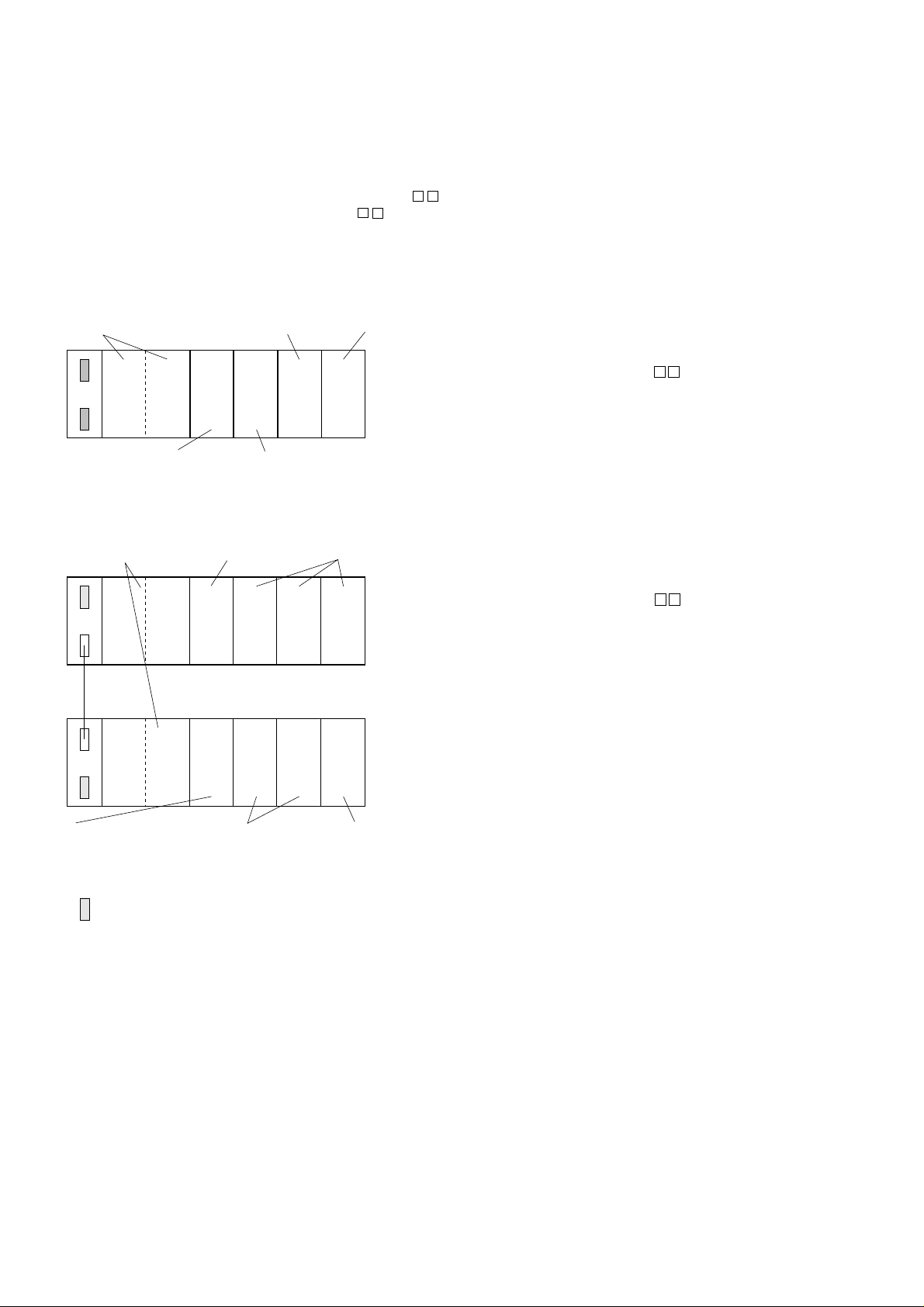
3-3-1 NP1F-MP1 (for 1 axis)
1) Status indication LED
2) External I/O signal
connector
ONL RDY
ERR ALM
EMG+OT-OT
1) Status indication LED
This LED indicates the operation status and the error status of NP1F-MP1. LED color means as shown below.
• Green: This is used to confirm the operation, not emergency.
• Red: Any fault status is detected, a state of emergency.
DELnoitacidnI emaN noitpircseD
)neerG(LNOlamronsubXS.lamronsisubXSnehwnosnruT
)deR(RRElamronbasubXS )revonoitaivedasaemaS(.subXSnisruccororrenanehwnosnruT
)neerG(YDRydaeR.lamronsieludomehtnehwnosnruT
)deR(MLArorrE .erawdrahehtniromargorpnoitacilppaehtnisruccororrenanehwnosnruT
)deR(GMEpotsycnegremE )etoN()tcatnocCN:langisO/IlanretxE(.NOsitupnipotsycnegremeehtnehwnosnruT
)deR(TO+levartrevO )etoN()tcatnocCN:langisO/IlanretxE(.NOsitupninoitceridsulpehtnehwnosnruT
- )deR(TO
levartrevO )etoN()tcatnocCN:langisO/IlanretxE(.NOsitupninoitceridsunimehtnehwnosnruT
Note: Indication LEDs (EMG/ ±OT) operate with the external input signal. Only the status of input signals are indicated.
3-4
Page 23

2) Connector pin layout for the external I/O signal
A front view Signal name
B/A
20
19
18
17
16
15
14
13
12
11
10
9
8
7
6
5
4
3
2
1
Connector pin layout (40-pin)
Connector
• NP1F-MP1 side
Connector ··· FCN-365P040-AU (Fujitsu)
··· FCN-360A2 (Fujitsu)
For details of the connector, refer to “4-6 I/O Wiring.”
20
19
18
17
16
15
14
13
12
11
10
9
8
7
6
5
4
3
2
1
.oNniP emanlangiS .oNniP emanlangiS
02BCDV4202ACDV42
91BCDV091ACDV0
81BMOC81AMOC
71BtupniTO-71AtupniGME
61BtupniTO+61AtupniSLnigirO
51B1MOCtupnI51AtupnitpurretnI
41B1MOCtupnI41A1MOCtupnI
31BCDV42:tuptuoroF31ACDV42:tuptuoroF
21B2oD21A1oD
11BMOCtuptuO11AMOCtuptuO
01BMOC01AMOC
9B
tuptuo
eslupesreveR
9A
8BMOCtuptuoesluP8AMOCtuptuoesluP
7B
B-esahp
6B
5B
4B
3B
2B
DNG
DNG
DNG
B-esahp
1B
eslupkcabdeeF
eslupkcabdeeF
B-esahp*
eslupkcabdeeF
B-esahp*
7A
6A
5A
tinuesluplaunaM
4A
tinuesluplaunaM
3A
tinuesluplaunaM
2A
tinuesluplaunaM
1A
3-3 Names
eslupdrawroF
tuptuo
eslupkcabdeeF
A-esahp
eslupkcabdeeF
A-esahp*
eslupkcabdeeF
DNG
eslupkcabdeeF
Z-esahp
eslupkcabdeeF
Z-esahp*
tinuesluplaunaM
A-esahp
tinuesluplaunaM
A-esahp*
*1 Manual pulse unit GND (B3, B4) are connected internal.
*2 Feedback pulse GND (A5, B5) are connected internal.
*3 Output COM (A11, B11) are connected internal.
*4 For output: 24V DC (A13, B13) are connected internal.
*5 Input COM1 (A14, B14, B15) are connected internal.
*6 0V DC (A19, B19) are connected internal.
*7 24V DC (A20, B20) are connected internal.
*8 A19, B19, A18, B18, A10 and B10 are connected internal.
3-5
Page 24
3-3 Names
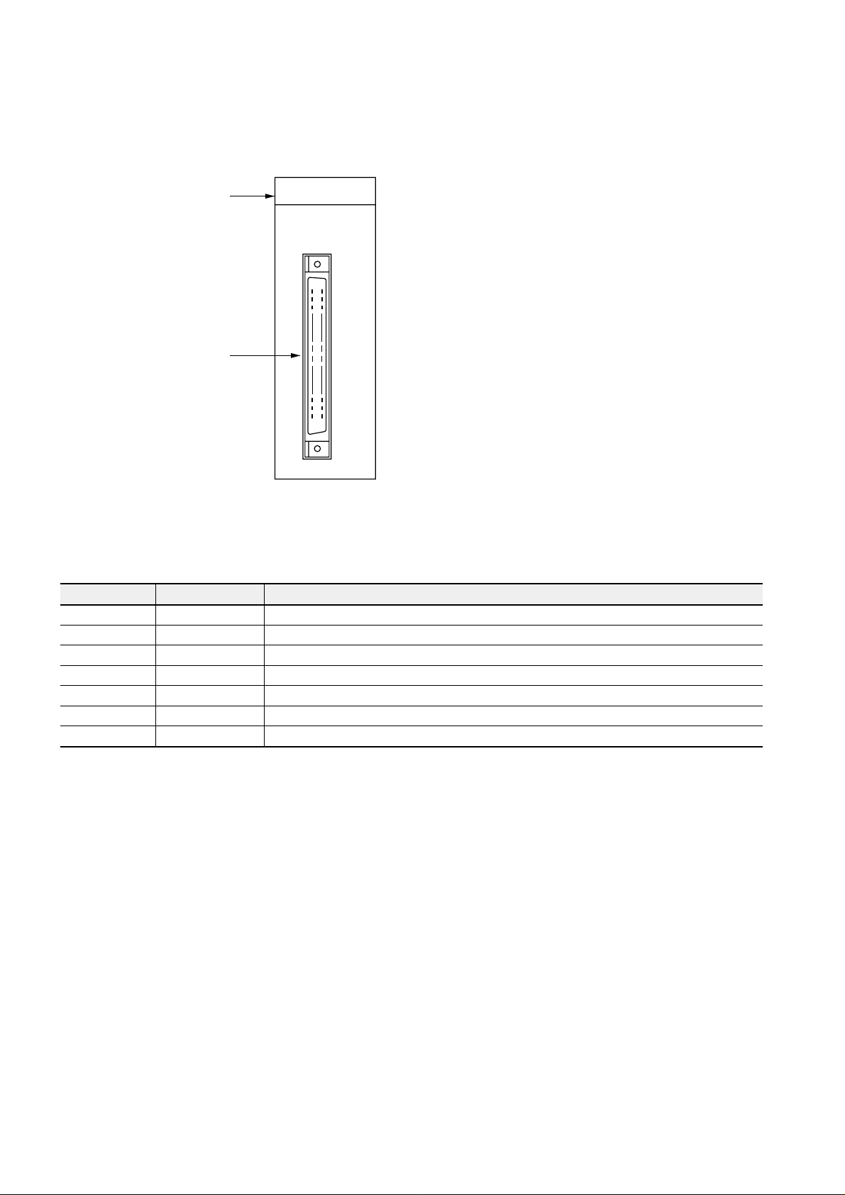
3-3-2 NP1F-MP2 (for 2 axes)
1) Status indication LED
2) External I/O signal connector
ONL RDY
ERR ALM
CH1
EMG+OT-OT
CH2
CH1 CH2
1) Status indication LED
This LED indicates the operation status and the error status of NP1F-MP2. LED color means as shown below.
• Green: This is used to confirm the operation,
not emergency.
• Red: Any fault status is detected, a state of emergency.
DELnoitacidnI
)2HC/1HC(
emaN
noitpircseD
)2HC/1HC(
)neerG(LNOlamronsubXS.lamronsisubXSnehwnosnruT
)deR(RRElamronbasubXS )revonoitaivedasaemaS(.subXSnisruccororrenanehwnosnruT
)neerG(YDRydaeR.lamronsieludomehtnehwnosnruT
)deR(MLArorrE .erawdrahehtniromargorpnoitacilppaehtnisruccororrenanehwnosnruT
)deR(GMEpotsycnegremE )etoN()tcatnocCN:langisO/IlanretxE(.NOsitupnipotsycnegremeehtnehwnosnruT
)deR(TO+levartrevO )etoN()tcatnocCN:langisO/IlanretxE(.NOsitupninoitceridsulpehtnehwnosnruT
- )deR(TO
levartrevO )etoN()tcatnocCN:langisO/IlanretxE(.NOsitupninoitceridsunimehtnehwnosnruT
Note: Indication LEDs (EMG/ ±OT) operate with the external input signal. Only the status of input signals are indicated.
3-6
Page 25

2) Connector pin layout for the external I/O signal
2HC
.oNniP emanlangiS .oNniP emanlangiS
02BCDV4202ACDV42
91BCDV091ACDV0
81BMOC81AMOC
71BtupniTO-71AtupniGME
61BtupniTO+61AtupniSLnigirO
51B2MOCtupnI51AtupnitpurretnI
41B2MOCtupnI41A2MOCtupnI
31BCDV42:tuptuoroF31ACDV42:tuptuoroF
21B2oD21A1oD
11BMOCtuptuO11AMOCtuptuO
01BMOC01AMOC
9B
eslupesreveR
tuptuo
9A
eslupdrawroF
tuptuo
8BMOCtuptuoesluP8AMOCtuptuoesluP
7B
eslupkcabdeeF
B-esahp
7A
eslupkcabdeeF
A-esahp
6B
eslupkcabdeeF
B-esahp*
6A
eslupkcabdeeF
A-esahp*
5B
eslupkcabdeeF
DNG
5A
eslupkcabdeeF
DNG
4BMOC4A
eslupkcabdeeF
Z-esahp
3BMOC3A
eslupkcabdeeF
Z-esahp*
2BC.N2AC.N
1BC.N1AC.N
A front view A front view
B/A
CH1
20
19
18
17
16
15
14
13
12
11
10
9
8
7
6
5
4
3
2
1
20
19
18
Usable connector
17
· NP1F-MP2 side
16
Connector
15
14
13
For details of the connector, refer to “4-6 I/O Wiring.”
12
11
10
9
8
7
6
5
4
3
2
1
··· FCN-365P040-AU (Fujitsu)
··· FCN-360A2 (Fujitsu)
3-3 Names
B/A
CH2
20
19
18
17
16
15
14
13
12
11
10
9
8
7
6
5
4
3
2
1
20
19
18
17
16
15
14
13
12
11
10
9
8
7
6
5
4
3
2
1
Connector pin layout (40-pin)
Signal name Signal name
1HC
.oNniP emanlangiS .oNniP emanlangiS
02BCDV4202ACDV42
91BCDV091ACDV0
81BMOC81AMOC
71BtupniTO-71AtupniGME
61BtupniTO+61AtupniSLnigirO
51B1MOCtupnI51AtupnitpurretnI
41B1MOCtupnI41A1MOCtupnI
31BCDV42:tuptuoroF31ACDV42:tuptuoroF
21B2oD21A1oD
11BMOCtuptuO11AMOCtuptuO
01BMOC01AMOC
9B
8BMOCtuptuoesluP8AMOCtuptuoesluP
7B
6B
5B
4B
3B
2B
1B
tuptuo
DNG
DNG
DNG
eslupesreveR
eslupkcabdeeF
B-esahp
eslupkcabdeeF
B-esahp*
eslupkcabdeeF
B-esahp
B-esahp*
Connector pin layout (40-pin)
9A
7A
6A
5A
tinuesluplaunaM
4A
tinuesluplaunaM
3A
tinuesluplaunaM
2A
tinuesluplaunaM
1A
DNG
eslupdrawroF
tuptuo
eslupkcabdeeF
A-esahp
eslupkcabdeeF
A-esahp*
Z-esahp
Z-esahp*
A-esahp
A-esahp*
eslupkcabdeeF
eslupkcabdeeF
eslupkcabdeeF
tinuesluplaunaM
tinuesluplaunaM
3-7
Page 26
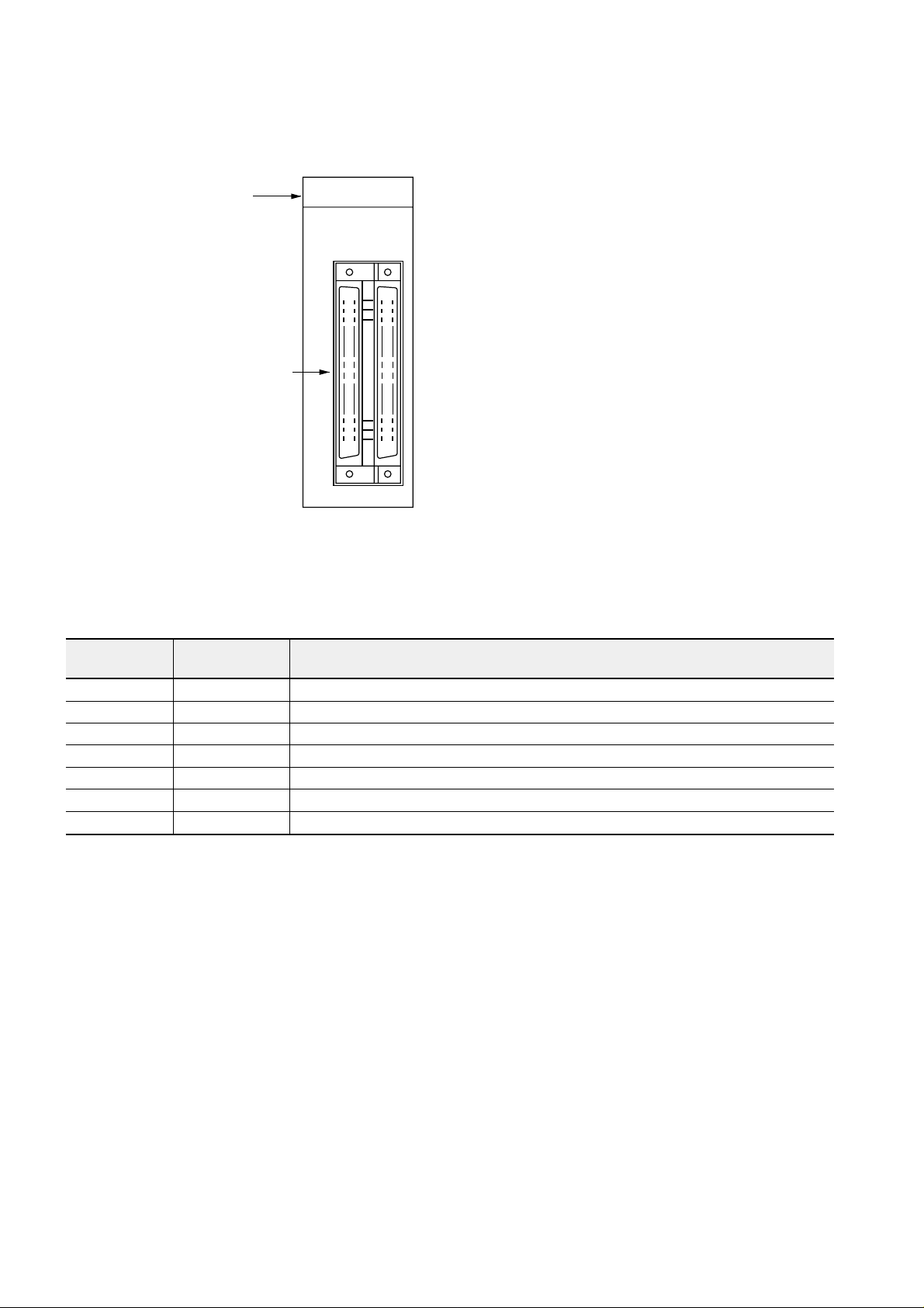
3-3 Names
3-3-3 NP2F-LEV (Signal converter)
PWR
LEV
1) Status indication LED
2) External I/O signal connector
1) Status indication LED
Status indication LED of NP2F-LEV
DELnoitacidnI emaN noitpircseD
)neerG(RWPylppusrewoplamroN.lamronsirewopCDV42nehwnosnruT
2) Connector pin layout for the external I/O signal
A front view (the upper side) A front view (the lower side)
Connector pin layout (9-pin) Connector pin layout (16-pin)
A
1
1
2
3
4
5
6
7
8
9
2
3
4
5
6
7
8
B
1
2
3
4
5
6
7
8
Usable connector Usable connector
· NP2F-LEV side · NP2F-LEVside
Connector ···· DELC-J9SAF-13L6 (JAE made) Connector ···· FCN-365P016-AU (Fujitsu)
Use the following connector cover Use the following connector cover
Connector ···· DE-9P-N (JAE made) Connector ···· FCN-361J016-AU (Fujitsu)
Cover ··········· DE-C1-J6 (JAE made) Cover ··········· FCN-360C016-B (Fujitsu)
3-8
Page 27

Signal name Signal name
.oNniP emanlangiS
1V0
2V0
3V0
4V0
5V0
6)1ON(tupnirotcerrocnepO
7)2ON(tupnirotcerrocnepO
8)3ON(tupnirotcerrocnepO
9)4ON(tupnirotcerrocnepO
.oNniP emanlangiS .oNniP emanlangiS
11A)P1ON(tuptuolaitnereffidV591B)N1ON(tuptuolaitnereffidV5
22A)P2ON(tuptuolaitnereffidV5012B)N2ON(tuptuolaitnereffidV5
33A)P3ON(tuptuolaitnereffidV5113B)N3ON(tuptuolaitnereffidV5
44A)P4ON(tuptuolaitnereffidV5214B)N4ON(tuptuolaitnereffidV5
55AV5_DNG315BV5_DNG
66ACN416BCN
77A)V42_DNG(CDV0517B)V42_DNG(CDV0
88ACDV42618BCDV42
3-3 Names
3-9
Page 28
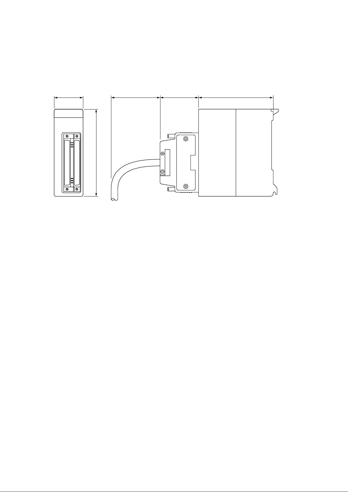
3-4 Dimensions
3-4-1 NP1F-MP1 (for 1 axis)
3-4-2 NP1F-MP2 (for 2 axes)
35
105
(75)
(46.5)
90
3-10
Page 29

3-4-3 NP2F-LEV (Signal converter)
39.8
29.8
10
85
95
(36)
3-4 Dimensions
95(47.2)
40
Ø6
3-11
Page 30

Section 4 Wiring
Page
4-1 Mounting Precautions ................................................................................................4-1
4-1-1 Number of mountable modules (NP1F-MP1/ NP1F-MP2).................................................... 4-1
4-1-2 Wiring precautions ................................................................................................................ 4-2
4-1-3 Wiring example of the external wiring connector .................................................................. 4-2
(1) Connector type ....................................................................................................................................... 4-2
(2) Connector cover type..............................................................................................................................4-2
4-2 Connector Pin Layout for the External Connection (NP1F-MP1) ........................... 4-3
4-2-1 External I/O signal specifications (NP1F-MP1)..................................................................... 4-4
4-2-2 External I/O signal interface (NP1F-MP1)............................................................................. 4-5
4-3 Connector Pin Layout for the External Connection (NP1F-MP2) ........................... 4-9
4-3-1 External I/O signal specifications (NP1F-MP2)................................................................... 4-10
4-3-2 External I/O signal interface (NP1F-MP2)........................................................................... 4-11
4-4 Connector Pin Layout for the External Connection (Signal Converter) .............. 4-17
4-4-1 External I/O signal specifications (Signal converter)........................................................... 4-18
4-4-2 External I/O signal interface (Signal converter) .................................................................. 4-19
4-5 Connecting .................................................................................................................4-21
4-5-1 Connecting sample of a servo motor .................................................................................. 4-21
(1) When the NP1F-MP1 or the NP1F-MP2 generates the forward pulse or the reverse pulse.................4-21
(2) Forward pulse command, reverse pulse command ..............................................................................4-21
(3) Connecting sample of FALDIC-II and NP1F-MP2................................................................................. 4-22
(4) Connecting sample of a stepping motor and NP1F-MP2 ..................................................................... 4-23
4-6 I/O Wiring ................................................................................................................... 4-24
(1) Wiring of a connector type module .......................................................................................................4-24
Page 31

Section 4 Wiring
)epyT(eludoM
tnerruC
noitpmusnoc
skrameR
UPCecnamrofrep-hgiHA2.0
lortnocgninoitisopsexa2
)2PM-F1PN(
A590.0
lortnocgninoitisopsexa2
)2AM-F1PN(
A51.0
lortnocgninoitisopsexa2
)2PH-F1PN(
A590.0
retnuocdeeps-hgiH
)2CH-F1PN(
A580.0
esopruplareneG
noitacinummoc
)1SR-L1PN(
A11.0
)2CP-F1PN(dracCPA21.0
)1SA-L1PN(i-SAA1.0
)1PJ-L1PN(1-NCPOA31.0
)1LP-L1PN(knil-PA61.0
)1LT-L1PN(retsamknil-TA41.0
4-1 Mounting Precautions
4-1-1 Number of mountable modules (NP1F-MP1/ NP1F-MP2)
To mount the NP1F-MP1 or the NP1F-MP2 to the base board where the CPU module and the power supply module are
mounted on, take the following precautions.
(1) The number of mountable modules to the base board in MICREX-SX is shown below.
1) Supplied power (Power supply module) 2) Current consumption
epyT )CDV42(tnerructuptuO
22-S1PNA64.1
24-S1PNA64.1
3) Current consumption of the positioning control module
NP1F-MP1: A/module
NP1F-MP2: 0.095A/module
For the current consumption of I/O module, refer to “Appendix-6 Current consumption and Mass of MICREX-SX series.”
Calculation method for the number of mountable modules
T-link master
CPU Base board
1.46A -(0.2A + 0.14A + 0.07)
0.095A (NP1F-MP2)
(2) Installation conditions of the positioning control module base on that conditions of MICREX-SX series.
User’s Manual Hardware, MICREX-SX series ····· FEH201
= 11.05 = 11 modules
4-1
Page 32

4-1 Mounting Precautions
4-1-2 Wiring precautions
Precautions of wiring the positioning control module and the external device are shown below.
1) The cable length between the positioning control module and the driver varies with the driver type. Confirm the
specifications of the driver.
2) I/O wiring
• Do not bundle up or close the I/O cables to the power cables or the main circuit cables.
• If these cables are closed near, separate the ducts or wire them separately.
• If I/O wiring cannot be separated from the power cables or the main circuit cables, bound shield cables must be
used and the shield must be grounded at the PC end.
• To wire the pulse output, shielded cables must be used.
• If the ducts are used for wiring, the ducts must be grounded.
4-1-3 Wiring example of the external wiring connector
(1) Connector type (2) Connector cover type
FCN-361J040-AU (Fujitsu) FCN-360C040-B (Fujitsu)
1) Let the wires through the heat-shrinkable tube. Let each wire
through the insulation tube, and solder them. The heat-shrinkable
tube is shrunk by a drier.
2) Mount the connector on the case (the lower,) and set the screw.
* Twist the wire in the connector case.
3) Put the case (the upper), and turn screws.
Insulation tube
Heat-shrinkable tube
Soldering
Connector
Case (the lower)
Screw
* For details of usable connector, refer to “4-6 I/O Wiring.”
4-2
Nut, screw and washer
Screw and nut
Page 33

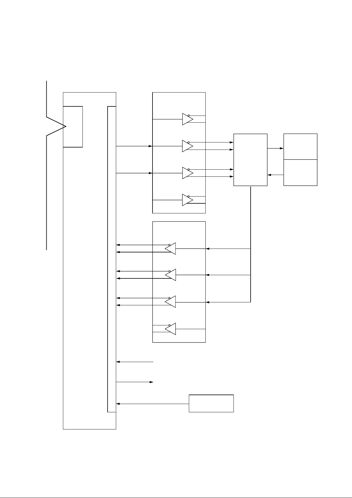
B/A
CH1
20
19
18
17
16
15
14
13
12
11
10
9
8
7
6
5
4
3
2
1
Connector pin layout (40-pin)
Usable connector
· NP1F-MP1 side
Connector···FCN-365P040-AU (Fujitsu)
···FCN-360A2 (Fujitsu)
20
19
18
17
16
15
14
13
12
11
10
9
8
7
6
5
4
3
2
1
4-2 Connector Pin Lay out for the External
Connection (NP1F-MP1)
Signal name
.oNniP emanlangiS .oNniP emanlangiS
02BCDV4202ACDV42
91BCDV091ACDV0
81BMOC81AMOC
71BtupniTO-71AtupniGME
61BtupniTO+61AtupniSLnigirO
51B1MOCtupnI51AtupnitpurretnI
41B1MOCtupnI41A1MOCtupnI
31BCDV42:tuptuoroF31ACDV42:tuptuoroF
21B2oD21A1oD
11BMOCtuptuO11AMOCtuptuO
01BMOC01AMOC
9BtuptuoeslupesreveR9AtuptuoeslupdrawroF
8BMOCtuptuoesluP8AMOCtuptuoesluP
7B
6B
5BDNGeslupkcabdeeF5ADNGeslupkcabdeeF
4B
3B
2B
1B
B-esahp
DNG
DNG
B-esahp
eslupkcabdeeF
eslupkcabdeeF
B-esahp*
tinuesluplaunaM
tinuesluplaunaM
tinuesluplaunaM
tinuesluplaunaM
B-esahp*
7A
6A
4A
3A
2A
1A
A-esahp
Z-esahp
A-esahp
eslupkcabdeeF
eslupkcabdeeF
A-esahp*
eslupkcabdeeF
eslupkcabdeeF
Z-esahp*
tinuesluplaunaM
tinuesluplaunaM
A-esahp*
*For details of usable connector, refer to “4-6 I/O Wiring.”
*1 Manual pulse unit GND (B3, B4) are connected internal.
*2 Feedback pulse GND (A5, B5) are connected internal.
*3 Output COM (A11, B11) are connected internal.
*4 For output: 24V DC (A13, B13) are connected internal.
*5 Input COM1 (A14, B14, B15) are connected internal.
*6 0V DC (A19, B19) are connected internal.
*7 24V DC (A20, B20) are connected internal.
*8 A19, B19, A18, B18, A10 and B10 are connected internal.
*9 For detail specifications of the above signals, refer to 4-2-1.
4-3
Page 34

4-2 Connector Pin Lay out for the External
Connection (NP1F-MP1)
4-2-1 External I/O signal specifications (NP1F-MP1)
emanlangiS lobmyslanimreT .oNniprotcennoC noitcnuF noitacificepS
A-esahp*tinuesluplaunaM1A-1HClangisA-esahptinuesluplaunamfotupnI
A-esahptinuesluplaunaM2A-1HClangisA-esahptinuesluplaunamfotupnI
tinuesluplaunaM
)tupnI(langisdnammoc
)tupnI(
)tuptuO(
langiseslupkcabdeeF
tupnitpurretnI51A-1HCreggirtgninoitisoptpurretnifotupnI
tupniSLnigirO61A-1HCSLnigirofotupnI
tupniGME71A-1HC)tcatnocCN(potsycnegremefotupnI
tupniTO-71B-1HC)tcatnocCN(noitceridsunimfotupnI
)tupnI(langistupnilanretxE
)tuptuO(langistuptuoesluP
langistuptuolanretxE
)tupnI(ylppusrewoP
tupniTO+61B-1HC)tcatnocCN(noitceridsulpfotupnI
1MOCtupnI41A-1HClangistupnilanretxerofrewopnommoC
1MOCtupnI41B-1HClangistupnilanretxerofrewopnommoC
1MOCtupnI51B-1HClangistupnilanretxerofrewopnommoC
MOCtuptuoesluP8A-1HCMOCesluP
MOCtuptuoesluP8B-1HCMOCesluP
1oD21A-1HClangistuptuolanretxeroF
2oD21B-1HClangistuptuolanretxeroF
MOCtuptuO11A-1HCylppusrewoplanretxefonommoC
MOCtuptuO11B-1HCylppusrewoplanretxefonommoC
CDV4202A-1HCylppusrewopV42+
CDV4202B-1HCylppusrewopV42+
CDV091A-1HCnommocylppusrewoP
CDV091B-1HCnommocylppusrewoP
B-esahp*tinuesluplaunaM1B-1HClangisB-esahptinuesluplaunamfotupnI
B-esahptinuesluplaunaM2B-1HClangisB-esahptinuesluplaunamfotupnI
DNGtinuesluplaunaM3B-1HClangisV0tinuesluplaunamfotupnI
DNGtinuesluplaunaM4B-1HClangisV0tinuesluplaunamfotupnI
A-esahp*eslupkcabdeeF6A-1HClangisA-esahpeslupkcabdeeffotupnI
A-esahpeslupkcabdeeF7A-1HClangisA-esahpeslupkcabdeeffotupnI
B-esahp*eslupkcabdeeF6B-1HClangisB-esahpeslupkcabdeeffotupnI
B-esahpeslupkcabdeeF7B-1HClangisB-esahpeslupkcabdeeffotupnI
Z-esahp*eslupkcabdeeF3A-1HClangisZ-esahpeslupkcabdeeffotupnI
Z-esahpeslupkcabdeeF4A-1HClangisZ-esahpeslupkcabdeeffotupnI
DNGeslupkcabdeeF5A-1HClangisV0eslupkcabdeeffotupnI
DNGeslupkcabdeeF5B-1HClangisV0eslupkcabdeeffotupnI
tuptuoeslupdrawroF9A-1HCeslupnoitceridsulP
tuptuoeslupesreveR9B-1HCeslupnoitceridsuniM
CDV42:tuptuoroF31A-1HC)TUPNI(ylppusrewoplanretxE
CDV42:tuptuoroF31B-1HC)TUPNI(ylppusrewoplanretxE
4-4
Page 35

4-2 Connector Pin Lay out for the External
4-2-2 External I/O signal interface (NP1F-MP1)
Signal name Circuit
Manual pulse unit command
signal
Connection (NP1F-MP1)
Manual pulse
unit side
Phase-A
Phase-B
0V
When the manual pulse unit utilizes open collectors.
A2
A1
B2
B1
B3
B4+5V
220Ω
220Ω
120Ω
120Ω
120Ω
120Ω
Phase-A
1.2kΩ
Phase-B
1.2kΩ
CH1 side
Manual pulse
unit side
Phase-A
Phase-B
0V
+5V
When the manual pulse unit is a line driver.
B3
A2
A1
B2
B1
B4
220Ω
220Ω
120Ω
120Ω
120Ω
120Ω
Phase-A
1.2kΩ
Phase-B
1.2kΩ
CH1 side
4-5
Page 36

4-2 Connector Pin Lay out for the External
Connection (NP1F-MP1)
Signal name
Feedback pulse signal
Circuit
Servo side
Phase-A
Phase-B
Phase-Z
+5V
A7
A6
B7
B6
A4
A3
A5
220Ω
220Ω
220Ω
120Ω
120Ω
120Ω
120Ω
120Ω
120Ω
Phase-A
1.2kΩ
Phase-B
1.2kΩ
Phase-Z
1.2kΩ
B5
When the feedback pulse signal is driven by a open collector.
Servo side
Phase-A
Phase-B
Phase-Z
A7
A6
B7
B6
A4
A3
A5
120Ω
220Ω
120Ω
120Ω
220Ω
120Ω
120Ω
220Ω
120Ω
CH1 side
Phase-A
1.2kΩ
Phase-B
1.2kΩ
Phase-Z
1.2kΩ
B5
When the feedback pulse signal is driven by a line driver.
4-6
CH1 side
Page 37

Signal name Circuit
External input signal
4-2 Connector Pin Lay out for the External
Connection (NP1F-MP1)
+OT
-OT
Emergency
stop
Origin LS
Interrupt
+24V
A14
B16
B17
A17
A16
A15
3.9kΩ
3.9kΩ
3.9kΩ
3.9kΩ
3.9kΩ
820Ω
820Ω
820Ω
820Ω
820Ω
CH1 side
Pulse output signal
CH1 side
When the servo device utilizes open collectors
A9
A8
B9
B8
CA
*CA
CB
*CB
CM
Servo side
4-7
Page 38

4-2 Connector Pin Lay out for the External
Connection (NP1F-MP1)
Signal name Circuit
External output signal
3.9kΩ
3.9kΩ
A13
A12
A11
B13
B12
+24V
Ry
Ry
CH1 side
B11
4-8
Page 39

4-3 Connector Pin Lay out for the External
Connection (NP1F-MP2)
CH1
20
19
18
17
16
15
14
13
12
11
10
9
8
7
6
5
4
3
2
1
B/A
Signal name Signal name
1HC
.oNniP emanlangiS .oNniP emanlangiS
02BCDV4202ACDV42
91BCDV091ACDV0
81BMOC81AMOC
71BtupniTO-71AtupniGME
61BtupniTO+61AtupniSLnigirO
51B1MOCtupnI51AtupnitpurretnI
41B1MOCtupnI41A1MOCtupnI
31B
21B2oD21A1oD
11BMOCtuptuO11AMOCtuptuO
01BMOC01AMOC
9B
8B
7B
6B
5B
4B
3B
2B
1B
*1 Manual pulse unit GND (B3, B4) are connected internal.
*2 Do not use NC terminals as repeating terminals.
*3 Feedback pulse GND (A5, B5) are connected internal.
*4 Output COM (A11, B11) are connected internal.
CD
tuptuo
MOC
B-esahp
DNG
Connector pin layout (40-pin)
20
19
18
Usable connector
17
· NP1F-MP2 side
16
Connector ··· FCN-365P040-AU (Fujitsu)
15
14
13
12
11
10
9
For details of usable connector, refer to “4-6 I/O Wiring.”
8
7
6
5
4
3
2
1
V42:tuptuoroF
eslupesreveR
tuptuoesluP
eslupkcabdeeF
eslupkcabdeeF
B-esahp*
eslupkcabdeeF
esluplaunaM
DNGtinu
esluplaunaM
DNGtinu
esluplaunaM
B-esahptinu
esluplaunaM
B-esahp*tinu
··· FCN-360A2 (Fujitsu)
31A
9A
8A
7A
6A
5A
4A
3A
2A
1A
CD
MOC
DNG
V42:tuptuoroF
eslupdrawroF
tuptuo
tuptuoesluP
eslupkcabdeeF
A-esahp
eslupkcabdeeF
A-esahp*
eslupkcabdeeF
eslupkcabdeeF
Z-esahp
eslupkcabdeeF
Z-esahp*
esluplaunaM
A-esahptinu
esluplaunaM
A-esahp*tinu
9B
8B
7B
6B
5B
4BMOC4A
3BMOC3A
2BC.N2AC.N
1BC.N1AC.N
2HC
.oNniP emanlangiS .oNniP emanlangiS
02BCDV4202ACDV42
91BCDV091ACDV0
81BMOC81AMOC
71BtupniTO-71AtupniGME
61BtupniTO+61AtupniSLnigirO
51B2MOCtupnI51AtupnitpurretnI
41B2MOCtupnI41A2MOCtupnI
31B
21B2oD21A1oD
11BMOCtuptuO11AMOCtuptuO
01BMOC01AMOC
4-9
CH2
B/A
31A
20
19
18
17
16
15
14
13
12
11
10
9
8
7
6
5
4
3
2
1
V42:tuptuoroF
CD
eslupdrawroF
tuptuo
tuptuoesluP
MOC
eslupkcabdeeF
A-esahp
eslupkcabdeeF
A-esahp*
eslupkcabdeeF
DNG
eslupkcabdeeF
Z-esahp
eslupkcabdeeF
Z-esahp*
20
19
18
17
16
15
14
13
12
11
10
9
8
7
6
5
4
3
2
1
V42:tuptuoroF
CD
eslupesreveR
tuptuo
tuptuoesluP
MOC
B-esahp
B-esahp*
DNG
9A
8A
eslupkcabdeeF
7A
eslupkcabdeeF
6A
eslupkcabdeeF
5A
Page 40

4-3 Connector Pin Lay out for the External
Connection (NP1F-MP2)
*5 For output: 24V DC (A13, B13) are connected internal.
*6 0V DC (A19, B19) are connected internal.
*7 24V DC (A20, B20) are connected internal.
*8 Input COM1 (A14, B14, B15) are connected internal. (Input COM1 and Input COM2 are not connected.)
*9 Input COM2 (A14, B14, B15) are connected internal. (Input COM1 and Input COM2 are not connected.)
*10 For detail specifications of the above signals, refer to 4-3-1.
4-3-1 External I/O signal specifications (NP1F-MP2)
emanlangiS lobmyslanimreT .oNniprotcennoC noitcnuF noitacificepS
edis1HC edis2HC
A-esahp*tinuesluplaunaM
A-esahptinuesluplaunaM
B-esahp*tinuesluplaunaM
B-esahptinuesluplaunaM
esluplaunaM
dnammoctinu
)tupnI(langis
kcabdeeF
langiseslup
)tupnI(
tupniGME
tupnilanretxE
)tupnI(langis
tupniTO-
tupniTO+
DNGtinuesluplaunaM
DNGtinuesluplaunaM
A-esahp*eslupkcabdeeF
A-esahpeslupkcabdeeF
B-esahp*eslupkcabdeeF
B-esahpeslupkcabdeeF
Z-esahp*eslupkcabdeeF
Z-esahpeslupkcabdeeF
DNGeslupkcabdeeF
DNGeslupkcabdeeF
tupnitpurretnI
tupniSLnigirO
2,1MOCtupnI
2,1MOCtupnI
2,1MOCtupnI
1A-1HC
2A-1HC
1B-1HC
2B-1HC
3B-1HC
4B-1HC
6A-1HC
7A-1HC
6B-1HC
7B-1HC
3A-1HC
4A-1HC
5A-1HC
5B-1HC
51A-1HC
61A-1HC
71A-1HC
71B-1HC
61B-1HC
41A-1HC
41B-1HC
51B-1HC
6A-2HC
7A-2HC
6B-2HC
7B-2HC
3A-2HC
4A-2HC
5A-2HC
5B-2HC
51A-2HC
61A-2HC
71A-2HC
71B-2HC
61B-2HC
41A-2HC
41B-2HC
51B-2HC
SLnigirofotupnI
langisA-esahptinuesluplaunamfotupnI
langisA-esahptinuesluplaunamfotupnI
langisB-esahptinuesluplaunamfotupnI
langisB-esahptinuesluplaunamfotupnI
langisV0tinuesluplaunamfotupnI
langisV0tinuesluplaunamfotupnI
langisA-esahpeslupkcabdeeffotupnI
langisA-esahpeslupkcabdeeffotupnI
langisB-esahpeslupkcabdeeffotupnI
langisB-esahpeslupkcabdeeffotupnI
langisZ-esahpeslupkcabdeeffotupnI
langisZ-esahpeslupkcabdeeffotupnI
langisV0eslupkcabdeeffotupnI
langisV0eslupkcabdeeffotupnI
reggirtgninoitisoptpurretnifotupnI
)tcatnocCN(potsycnegremefotupnI
)tcatnocCN(noitceridsunimfotupnI
)tcatnocCN(noitceridsulpfotupnI
langistupnilanretxerofrewopnommoC
langistupnilanretxerofrewopnommoC
langistupnilanretxerofrewopnommoC
CDV5egatlovtupnidetaR
tniop/Am04tnerructupnidetaR
,tupniknistamroftupnI
langislaitnereffid
011ecnadepmitupnI Ω sselro
ycneuqerfesluptupnI
sppk005.xaM
eromroV5.3egnaregatlovNO
V5.1ot0egnaregatlovFFO
emityaledtupnI
1:NOotFFO µ sselros
1:FFOotNO µ sselros
CDV5egatlovtupnidetaR
tniop/Am04tnerructupnidetaR
,tupniknistamroftupnI
langislaitnereffid
011ecnadepmitupnI Ω sselro
ycneuqerfesluptupnI
sppk005.xaM
eromroV5.3egnaregatlovNO
V5.1ot0egnaregatlovFFO
emityaledtupnI
1:NOotFFO µ sselros
1:FFOotNO µ sselros
CDV42egatlovtupnidetaR
tniop/Am6tnerructupnidetaR
k9.3ecnadepmitupnI Ω sselro
V03ot51egnaregatlovNO
V5ot0egnaregatlovFFO
emityaledtupnI
sselrosm5:NOotFFO
sselrosm5:FFOotNO
MOCtuptuoesluP
tuptuoeslupdrawroF
tuptuoesluP
)tuptuO(langis
1oD
2oD
tuptuolanretxE
)tuptuO(langis
CDV42
ylppusrewoP
)tupnI(
CDV42
CDV0
CDV0
MOCtuptuoesluP
tuptuoeslupesreveR
MOCtuptuO
MOCtuptuO
CDV42:tuptuoroF
CDV42:tuptuoroF
8A-1HC
9A-1HC
8B-1HC
9B-1HC
21A-1HC
21B-1HC
11A-1HC
11B-1HC
31A-1HC
31B-1HC
02A-1HC
02B-1HC
91A-1HC
91B-1HC
8A-2HC
9A-2HC
8B-2HC
9B-2HC
21A-2HC
21B-2HC
11A-2HC
11B-2HC
31A-2HC
31B-2HC
02A-2HC
02B-2HC
91A-2HC
91B-2HC
MOCesluP
MOCsulP
MOCnoitceridsulP
eslupnoitceridsuniM
langistuptuolanretxeroF
langistuptuolanretxeroF
ylppusrewoplanretxefonommoC
ylppusrewoplanretxefonommoC
)TUPNI(ylppusrewoplanretxE
)TUPNI(ylppusrewoplanretxE
ylppusrewopCDV42+
ylppusrewopCDV42+
nommocylppusrewoP
nommocylppusrewoP
Am04/CDV42
emityaledtuptuO
tniop/A1.0.xaM
emityaledtuptuO
CDV42 ± %01
tuptuoknistamroftuptuO
ycneuqerfesluptuptuO
sppk052.xaM
sselrosm1:NOotFFO
sselrosm1:FFOotNO
tuptuoknistamroftuptuO
A3.0tnerrucegruS
sm01htgnertsegruS
sselrosm1:NOotFFO
sselrosm1:FFOotNO
4-10
Page 41

4-3-2 External I/O signal interface (NP1F-MP2)
Signal name Circuit
Manual pulse unit command
signal
120Ω
Phase-A
Phase-B
Phase-A
Phase-B
120Ω
1.2kΩ
A2
A1
120Ω
120Ω
1.2kΩ
220Ω
220Ω
B2
B1
B3
B4+5V
0V
Manual pulse
unit side
CH1 side
When the manual pulse unit utilizes open collectors.
When the manual pulse unit is a line driver.
120Ω
Phase-A
Phase-B
120Ω
1.2kΩ
A2
A1
120Ω
120Ω
1.2kΩ
220Ω
220Ω
B2
B1
B3
B4
CH1 side
+5V
0V
Phase-A
Phase-B
Manual pulse
unit side
4-3 Connector Pin Lay out for the External
Connection (NP1F-MP2)
4-11
Page 42

4-3 Connector Pin Lay out for the External
Connection (NP1F-MP2)
Signal name Circuit
Feedback pulse signal
Servo side
Phase-A
Phase-B
Phase-Z
+5V
A7
A6
B7
B6
A4
A3
A5
B5
220Ω
220Ω
220Ω
120Ω
120Ω
120Ω
120Ω
120Ω
120Ω
Phase-A
1.2kΩ
Phase-B
1.2kΩ
Phase-Z
1.2kΩ
CH1 side
Servo side
Phase-A
Phase-B
Phase-Z
When the feedback pulse signal is driven by a open collector.
+5V
A7
A6
B7
B6
A4
A3
A5
B5
120Ω
220Ω
120Ω
120Ω
220Ω
120Ω
120Ω
220Ω
120Ω
Phase-A
1.2kΩ
Phase-B
1.2kΩ
Phase-Z
1.2kΩ
CH2 side
4-12
Page 43

Signal name Circuit
Feedback pulse signal
Servo side
Phase-A
4-3 Connector Pin Lay out for the External
Connection (NP1F-MP2)
A7
A6
120Ω
220Ω
120Ω
Phase-A
1.2kΩ
Phase-B
Phase-Z
Servo side
Phase-A
B7
B6
A4
A3
A5
B5
A7
A6
220Ω
220Ω
220Ω
120Ω
120Ω
120Ω
120Ω
120Ω
120Ω
Phase-B
1.2kΩ
Phase-Z
1.2kΩ
CH1 side
Phase-A
1.2kΩ
B7
Phase-B
B6
A4
Phase-Z
A3
A5
B5
When the feedback pulse signal is driven by a line driver.
4-13
220Ω
220Ω
120Ω
120Ω
120Ω
120Ω
Phase-B
1.2kΩ
Phase-Z
1.2kΩ
CH2 side
Page 44

4-3 Connector Pin Lay out for the External
Connection (NP1F-MP2)
Signal name Circuit
External input signal
+OT
-OT
Emergency
stop
Origin LS
Interrupt
+24V
CH1-A14
CH1-B16
CH1-B17
CH1-A17
CH1-A16
CH1-A15
3.9kΩ
3.9kΩ
3.9kΩ
3.9kΩ
3.9kΩ
820Ω
820Ω
820Ω
820Ω
820Ω
CH1 side
+OT
-OT
Emergency
stop
Origin LS
Interrupt
+24V
CH2-A14
CH2-B16
CH2-B17
CH2-A17
CH2-A16
CH2-A15
3.9kΩ
3.9kΩ
3.9kΩ
3.9kΩ
3.9kΩ
820Ω
820Ω
820Ω
820Ω
820Ω
CH2 side
4-14
Page 45

Signal name Circuit
Pulse output signal
4-3 Connector Pin Lay out for the External
Connection (NP1F-MP2)
CH1 side
A9
A8
B9
B8
A9
CA
*CA
CB
*CB
CM
Servo side
CA
CH2 side
When the servo device utilizes open collectors.
A8
B9
B8
*CA
CB
*CB
CM
Servo side
4-15
Page 46

4-3 Connector Pin Lay out for the External
Connection (NP1F-MP2)
Signal name Circuit
External output
signal
3.9kΩ
3.9kΩ
A13
A12
A11
B13
B12
B11
+24V
Ry
Ry
CH1 side
3.9kΩ
3.9kΩ
A13
A12
A11
B13
B12
+24V
Ry
Ry
CH2 side
B11
4-16
Page 47

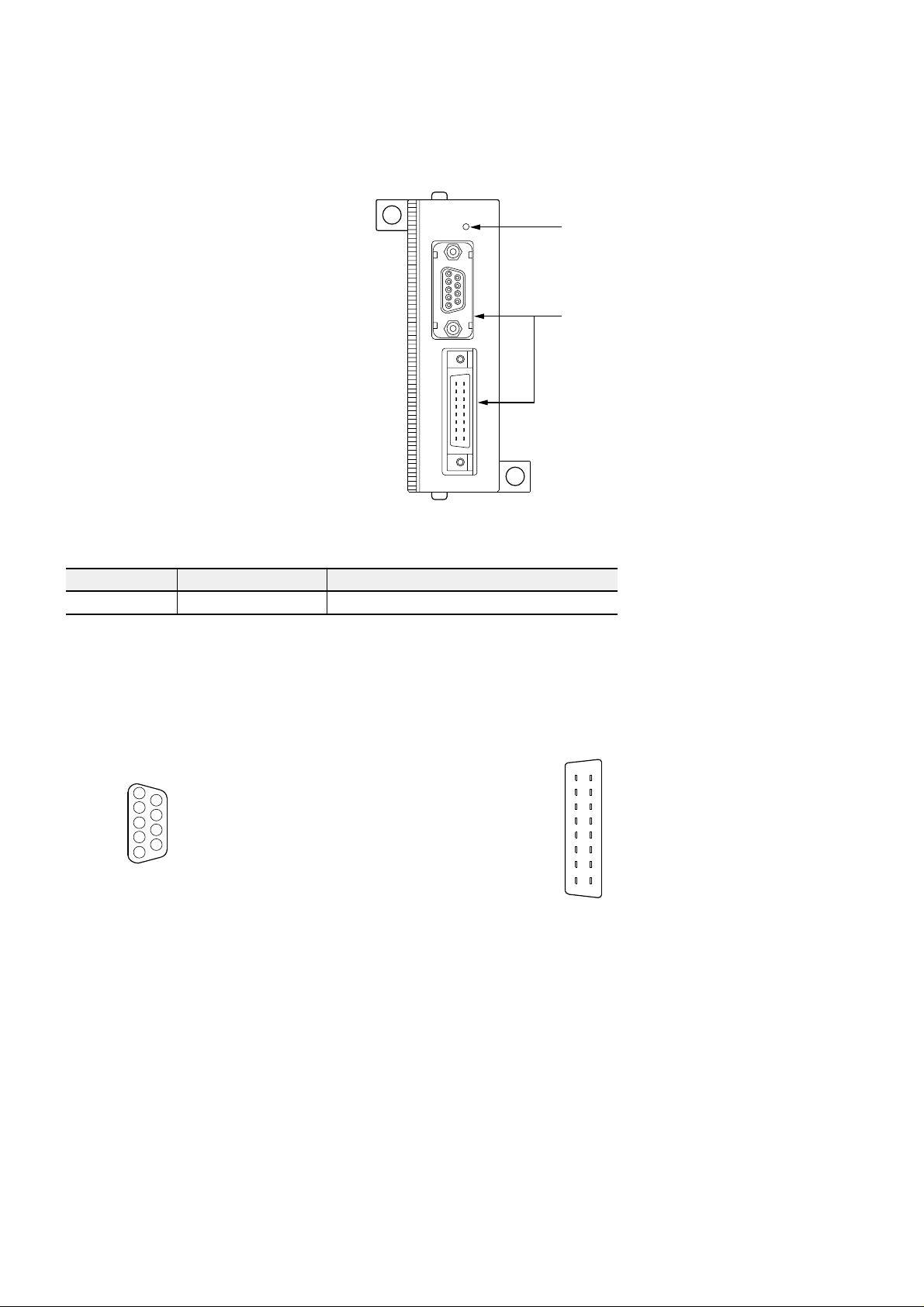
4-4 Connector Pin Lay out for the External
A front view (the upper side) Signal name
Connection (Signal Converter)
Connector pin layout (9-pin)
1
2
3
4
5
Usable connector
• NP2F-LEV side
Connector···DELC-J9SAF-13L6 (JAE made)
Use the following connector and cover.
Connector ··· DE-9P-N (JAE made)
Cover ·········· DE-C1-J6 (JAE made)
A front view (the lower side) Signal name
Connector pin layout (16-pin)
A
1
2
3
4
5
6
7
8
6
7
8
9
B
1
2
3
4
5
6
7
8
.oNniP emanlangiS
1V0
2V0
3V0
4V0
5V0
61tupnirotcerrocnepO
72tupnirotcerrocnepO
83tupnirotcerrocnepO
94tupnirotcerrocnepO
.oNniP emanlangiS .oNniP emanlangiS
11A)P1TUO(tuptuolaitnereffidV591B)N1TUO(tuptuolaitnereffidV5
22A)P2TUO(tuptuolaitnereffidV5012B)N2TUO(tuptuolaitnereffidV5
33A)P3TUO(tuptuolaitnereffidV5113B)N3TUO(tuptuolaitnereffidV5
44A)P4TUO(tuptuolaitnereffidV5214B)N4TUO(tuptuolaitnereffidV5
55AV5_DNG315BV5_DNG
66ACN416BCN
77A)V42_DNG(CDV0517B)V42_DNG(CDV0
88ACDV42618BCDV42
Usable connector
• NP2F-LEV side
Connector ··· FCN-365P016AU (Fujitsu)
Use the following connector and cover.
Connector ··· FCN-361J016-AU (Fujitsu)
Cover ·········· FCN-360C016-B (Fujitsu)
4-17
Page 48

4-4 Connector Pin Lay out for the External
Connection (Signal Con verter)
4-4-1 External I/O signal specifications (Signal converter)
emanlangiS lobmyslanimreT .oNniprotcennoC noitcnuF noitacificepS
nommoctupnI
langistupniroF
)nip-9(
rotcennocedistupnI
rotcennocedistuptuO
)nip-61(
langistupniroF
langistupniroF
langistupniroF
nommoctuptuO1B
langistuptuoroF1A
6
7
8
9
ylppusrewoprofnommoC5B,5A
ylppusrewoproftupnI8B,8AedisV42+
5,4,3,2,1
2B
3B
4B
2A
3A
4A
nommocedisV5
7B,7A
langistupnirofnommoC
)1NI(langistupniroF
)2NI(langistupniroF
)3NI(langistupniroF
)4NI(langistupniroF
)1TUO(langistuptuorofnommoC
)2TUO(langistuptuorofnommoC
)3TUO(langistuptuorofnommoC
)4TUO(langistuptuorofnommoC
)1TUO(langistuptuoroF
)2TUO(langistuptuoroF
)3TUO(langistuptuoroF
)4TUO(langistuptuoroF
nommocedisV42
emityaledtupnI
1:NOotFFO
µ
1:FFOotNO
µ
Am02tnerructupnidetaR
,tupniknistamroftupnI
022ecnadepmitupnI
Ω
eromroV5.3egnaregatlovNO
V5.1ot0egnaregatlovFFO
sselros
sselros
CDV5egatlovdetaR
584-SRtamroftuptuO
Am04.xaMtnerrucdaoL
4-18
Page 49

4-4-2 External I/O signal interface (Signal converter)
Signal name Circuit
Input side connector (9-pin)
220Ω
390Ω
10kΩ
+5V
220Ω
390Ω
10kΩ
+5V
220Ω
390Ω
10kΩ
+5V
220Ω
390Ω
10kΩ
+5V
6
7
8
9
1
2
3
4
5
A9
A8
B9
B8
CH1 side
(Pulse output)
Converter side
4-4 Connector Pin Lay out for the External
Connection (Signal Converter)
4-19
Page 50

4-4 Connector Pin Lay out for the External
Connection (Signal Con verter)
Signal name Circuit
Output side connector
(16-pin)
A1
B1
A2
B2
A3
B3
A4
B4
A8
A7
B8
B7
A5
0V
Servo side
+24V
Connector side
4-20
B5
Page 51

4-5 Connecting
4-5-1 Connecting sample of a servo motor
The relationship between the pulse generated by the NP1F-MP1 or the NP1F-MP2 and the rotation of a servo motor is as
shown below.
Note: Forward rotation and reverse rotation of the FUJI’s servo motor are reserved for other manufactures.
The direction indication of the motor rotation is
the shaft view from the motor mounted side.
CCW
(Counterclockwise) Forward rotationCW (Clockwise) Reverse rotation
(1) When the NP1F-MP1 or the NP1F-MP2 generates the forward pulse or the reverse pulse
Forward pulse····CCW
Reverse pulse····CW
(at 2-phase pulse input)
“H”
CCW
CW
Plus direction pulse
“H”
“H”“H”
Minus direction pulse
Forward pulse
Reverse pulse
(2) Forward pulse command, reverse pulse command
Forward pulse
Reverse pulse
Command pulse is output as 50% duty rate.
H
L
H
L
4-21
Page 52

4-5 Connecting
(3) Connecting sample of FALDIC-II and NP1F-MP2
Pulse train positioning
control combined module
NP1F-MP2
Servo amplifier
RYG***HA-VV
Servo motor
GRH***BG-**
Forward pulse output
Pulse output COM
Reverse pulse output
Pulse output COM
E5V
Feedback pulse
Feedback pulse
Feedback pulse
Feedback pulse
Feedback pulse
Feedback pulse
Feedback pulse
Feedback pulse
Manual pulse unit
Manual pulse unit
Manual pulse unit
Manual pulse unit
Manual pulse unit
Manual pulse unit
phase-A
*phase-A
phase-B
*phase-B
phase-Z
*phase-Z
GND
GND
*phase-A
phase-A
*phase-B
phase-B
GND
GND
A9
A8
B9
B8
A7
A6
B7
B6
A4
A3
A5
B5
A1
A2
B1
B2
B3
B4
+
DC5V
9
CA
CN1
*
CA
34
CB
10
*
CB
-
35
33
36
38
40
39
41
3
5
4
M5
FA
M5
FB
FZ
M5
M5
P10
VIN1
M5
28 N10
7
VIN2
6
M5
30
VIN3
29
M5
32
VIN4
31
M5
M5
M5
*
*
*
*
*
*
P5
P5
U
V
W
E
1
CN2
2
13
14
9
A
A
20
B
8
Dedicated cable
B
19
Z
7
Z
18
1
6
1
17
2
5
2
16
3
4
3
15
RYWE810
U
V
W
E
14
8
1
2
3
4
5
6
7
8
9
10
11
12
15
+5V
OV
A
*
B
*
Z
*
1
*
2
*
3
*
Shield
A
B
Z
1
2
3
Motor
Encoder
Output COM
Output COM
For output: 24V DC
For output: 24V DC
Input COM
Input COM
0V DC
0V DC
24V DC
24V DC
Do1
Output COM
Do2
Interrupt input
Input COM
Origin LS
EMG
-OT input
+OT input
A11
B11
A13
B13
A14
B14
A19
B19
A20
B20
A12
B12
A15
A16
A17
B17
B16
P24
N24
External I/O
N24
+24V
DC
Power
supply
0V
P24
N24
PC
PC
25
P24
24
P24
18
M24
17
M24
50 CONT1
(RUN)
49 CONT2
(FWD)
48 CONT3
(REV)
47 CONT4
(RST)
46 CONT5
(X1)
23 CONT6
(X2)
CONT7
22
(Pulse train magnification)
21 CONT8
(P function)
30B
TB
30C
CN1
(
Zero deviation
M24
M5
(RDY)
P24
12
45OUT1
44OUT2
43OUT3
42OUT4
20OUT5
19OUT6
26M5
27M5
P24
PC
)
2MON1
1MON2
R
S
T
Note: When the emergency stop is
input to the servo amplifier,
assign it to the CONT signal.
Power
supply
3ø
200V
4-22
Page 53

(4) Connecting sample of a stepping motor and NP1F-MP2
Pulse train positioning
control combined module
NP1F-MP2
Stepping motor
driver
4-5 Connecting
Forward pulse
Pulse output
Reverse pulse
Pulse output
E5V
Feedback pulse
Feedback pulse
*phase-Z
Feedback pulse
Feedback pulse
Output COM
For output: 24V DC
Input COM1
24V DC
Input COM1
Input COM
Origin LS
-OT input
+OT input
output
COM
output
COM
phase-Z
GND
GND
0V DC
EMG
A9
A8
B9
B8
A4
A3
A5
B5
A11
A13
A14
A19
A20
A15
A16
A17
B17
B16
+24V
+5V
+CW
-CW
+CCW
-CCW
TIM
COM
Stepping motor
BLACK
RED
GREEN
BLUE
AC100V
AC100V
4-23
Page 54

4-6 I/O Wiring
•I/O wiring depends on the module type, connected external devices, electrical specifications and the environment.
(1) Wiring of a connector type module
Usable connector and applicable cable size are shown below.
noitacifissalC )ustijuF(epyT eziselbaC
epytderedloS:tekcoS
UA-040J163-NCF
Soldered type
:revocrotcennoC
B-040C063-NCF
sselro32GWA
2
mm62.0(
)sselro
4-24
Page 55

Section 5 Memory Map
Page
5-1 NP1F-MP1/NP1F-MP2 Memory Map (Internal Memory List)....................................5-1
5-2 NP1F-MP1 I/O Area ..................................................................................................... 5-2
5-2-1 NP1F-MP1 (read area: address No. 0 to No. 9) .................................................................... 5-3
(1) Bit data signal (status signal, address No. “0,” lower word)..................................................................... 5-3
(2) Bit data signal (Status signal, address No. 1, upper word) ...................................................................5-12
(3) Current value read (Address No. 2: lower word; address No. 3: upper word)........................................5-16
(4) Current command value read (Address No. 4: lower word; address No. 5: upper word)....................... 5-16
(5) External pulse input counter (Address No. 8) ....................................................................................... 5-16
(6) Module detection time (Address No. 9) .................................................................................................5-17
(7) Current external pulse data (Address No. 6: lower word; address No. 7: upper word)..........................5-17
5-2-2 NP1F-MP1 (Write area: address Nos. 10 to 13) ................................................................. 5-18
(1) Bit command signal (write signal, address No. 10, lower word)............................................................ 5-18
(2) Bit command signal (Write signal, address No. 11, upper word) ..........................................................5-30
(3) Set value area (Write signal, address Nos. 12 and 13)......................................................................... 5-34
5-3 I/O Area of NP1F-MP2 ............................................................................................... 5-35
5-3-1 NP1F-MP2 (Read area: address No. 0 to No. 13)............................................................... 5-36
(1) Ch1 bit data signal (Status signal, address No. 0, lower word).............................................................5-36
(2) Ch1 bit data signal (Status signal, address No. 1, upper word) ............................................................ 5-46
(3) Ch1 current value read (Address No. 2: lower word; address No. 3: upper word) .................................5-50
(4) Current command value read (Address No. 4: lower word; address No. 5: upper word)....................... 5-50
(5) Ch2 bit data signal (Status signal, address No. 6, lower word).............................................................5-51
(6) Ch2 bit data signal (status signal, address No. 7, upper word).............................................................5-61
(7) Current value read (Address No. 8: lower word; address No. 9: upper word)........................................5-65
(8) Current command value read (Address No. 10: lower word; address No. 11: upper word)................... 5-65
(9) External pulse input counter (Address No. 12) ..................................................................................... 5-65
(10) Module detection time (Address No. 13) .............................................................................................5-66
5-3-2 NP1F-MP2 (Write area: address Nos. 14 to 21) ................................................................. 5-67
(1) Ch1 bit command signal (Write area, address No. 14, lower word) ......................................................5-67
(2) Ch1 bit command signal (Write signal, address No. 15, upper word) ................................................... 5-79
(3) Ch1 set value area (Write signal, address Nos. 16 and 17).................................................................. 5-82
(4) Ch2 bit command signal (write signal, address No. 18, lower word)..................................................... 5-83
(5) Ch2 bit command signal (Write signal, address No. 19, upper word) ................................................... 5-95
(6) Set value area (Write signal, address Nos. 20 and 21)......................................................................... 5-98
5-4 Setting Method and Effective Bits of Individual Register .....................................5-99
Page 56

5-1 NP1F-MP1/NP1F-MP2 Memory Map
The memory map for the NP1F-MP1/NP1F-MP2 is shown below.
Data is passed from the CPU via an SX bus and I/O area (I/Q area).
[CPU program]
SX bus
Section 5 Memory Map
(Internal Memory List)
I/O area
(occupies 22/14 words)
Write
Read
.oNsserddA emaN
0retsigerycneuqerftegraT
1retsigerycneuqerfesaB
2retsigerycneuqerftnerruC
3retsigereslupdnammoC
4retsigertniopnoitareleceD
51retsigernoitareleced/noitareleccA
62retsigernoitareleced/noitareleccA
7retsigernoitacilpitlumdeepS
8retnuoceslupdnammoC
:
:
:
13devreseR
)yromemlanretnI(pamyromem2PM-F1PN/1PM-F1PN
:
:
:
5-1
Page 57

5-2 NP1F-MP1 I/O Area
The NP1F-MP1I/O area (I/Q area) is shown below:
Address No.
0 Bit data signal
1 Bit data signal
2 Current value read
3
4
5
6
7
8
14 13 12 11 10 9 8 7 6 5 4 3 2 1
15
lower word
PC <== MP1
upper word
PC <== MP1
lower word
PC <== MP1
Current value read
Current command value read
Current command value read
Current external pulse data read
Current external pulse data read
External pulse input counter
upper word
PC <== MP1
lower word
PC <== MP1
upper word
PC <== MP1
lower word
PC <== MP1
upper word
PC <== MP1
PC <== MP1
0 Remarks
PC
<==
MP1
Read area
9
10 Bit command signal
11 Bit command signal
12 Set value area
13 Set value area
The NP1F-MP1 I/O area occupies 14 words.
Module detection time
lower word
PC ==> MP1
upper word
PC ==> MP1
lower word
PC ==> MP1
upper word
PC ==> MP1
PC <== MP1
PC
<==
MP1
Write area
5-2
Page 58

5-2 NP1F-MP1 I/O Area
5-2-1 NP1F-MP1 (read area: address No. 0 to No. 9)
(1) Bit data signal (status signal, address No. “0,” lower word)
.oNtiB emanlangiS noitpircseD
0
1
2dnegninoitisoP .dednesahgninoitisoprofnoitarepoehtnehw"NO"
3
4
5
6noitcetedlangisZ-esahP .detcetedsiZ-esahpnehw"NO",delbanesinoitcetedlangisZ-esahpelihW
7
8
9gnitareleced/gnitareleccAnoitareleced/noitareleccagnirud"NO"
01rorrepotsycnegremE .detcetedsirorrepotsycnegremenehw"NO"
11rorreTO+.detcetedsirorreTO+nehw"NO"
21rorreTO-.detcetedsirorreTO-nehw"NO"
31)desutoN("0"syawlA
41rorrerevotnuomanoitaiveD .detcetedsirorrerevotnuomanoitaivedehtnehw"NO"
51rorrenoissimsnarT .detcetedsirorrenoissimsnartnehw"NO" )1etoN(
orez-raeN orez-raenehtnihtiwsitnuomanoitaivedehtrofeulavetulosbaehtelihw"NO"
orezeslupdnammoC reffubOFIFehtdna"0"siretsigereslupdnammocehtfoeulavehtelihw"NO"
noitceridnoitatortnerruC gniebsieslupesrevernehw"NO";tuptuogniebsieslupdrawrofnehw"FFO"
eulavtnerrucotesnopseR
teserretnuoc
deepsgnignahC si)retsigerycneuqerftegrat(ataddeepsfognitirwsuounitnoc",NO"elihW
noitcetednoitisoptpurretnI silangistpurretniehtnehw"NO",delbanesinoitcetedlangistpurretnielihW
noitisoptpurretniesluplanretxE
noitceted
.htdiw
.eerfsi
.tuptuo
dnammocteserretsiger
.detucexe
.detceted
.detceted
eslupdnammocdna,dnammocteserretnuoceulavtnerrucotlangisesnopseR
silangistpurretniehtnehw"NO",delbanesinoitcetedlangistpurretnielihW
For a detailed explanation of individual signal names, refer to the following pages.
Note 1: The transmission error detect signal is output to channel 1.
5-3
Page 59

5-2 NP1F-MP1 I/O Area
1) Description of individual signal names
)orez-raeN:emanlangiS(0tiB
<Description>
• This signal is “1” while the deviation amount is within the setting range of the near-zero monitoring register.
Absolute value of the deviation amount ≤ Near-zero monitoring register
Precaution:
Because the deviation amount is always “0” when
feedback pulse is disabled, this signal is always “1.”
)orezeslupdnammoC:emanlangiS(1tiB
<Description>
• In pulse generation mode, the status of this signal becomes “1” (one) when the “command pulse register” is “0”
(zero) and the FIFO buffer is cleared.
The status of the “command pulse register” becomes “1” (one) when pulse output is completed or when command
pulse register reset signal is issued.
Select register
(PC == > MP1)
Set value data
(PC == > MP1)
Write command
(PC == > MP1)
Response to write
command (PC <== MP1)
Start command
(PC == > MP1)
Positioning end
(PC <== MP1)
Near-zero
(PC <== MP1)
Command pulse
zero (PC <== MP1)
(00011)
(10,000)
“1”
“1”
“1”
“1”
Pulse
“1”
“1”“1”
outputting
“1”
“1”
· In the position command mode
· Becomes “0” while pulse is output
Precaution:
With this module, positioning data can be registered in the FIFO buffer.
The command pulse zero signal becomes “0” while unexecuted positioning data exists in the FIFO buffer.
When positioning by the data registered in the FIFO buffer has all been completed or when the command pulse
register reset command is issued, the FIFO buffer becomes free.
5-4
Page 60

5-2 NP1F-MP1 I/O Area
Positioning end signal is “0” because
the command pulse is being output.
Positioning end signal is “1” because
the positioning end signal has been detected.
Outputting command pulse
(internal signal)
Near-zero
(PC <== MP1)
Positioning end
(PC <== MP1)
“1”
“1”“1”“0”
“1”
)dnegninoitisoP:emanlangiS(2tiB
<Description>
• In the pulse generation mode, this signal becomes “1” when the positioning operation has ended. This signal also
becomes “1” when command pulse output is stopped or when the near-zero signal is “1” and the start command
signal is “0.”
After the positioning end signal becomes “1,” this signal continues to be “1” even if the near-zero signal changes.
Precautions:
This signal becomes “0” while the start command is “1.”
• In the position command mode, the positioning end signal becomes “0” while the start command is “1.”
When the start command becomes “0,” pulse output is immediately stopped.
After this, the positioning end signal becomes “1” when the near-zero signal becomes “1.”
Start command
(PC == > MP1)
Near-zero
(PC <== MP1)
Positioning end
(PC <== MP1)
Operates according to position data.
“1”
“1”
“1”
5-5
Page 61

5-2 NP1F-MP1 I/O Area
(
)
)noitceridnoitatortnerruC:emanlangiS(3tiB
<Description>
• Indicates which direction to output the command pulse in.“0”: Forward; “1”: Reverse
The bit data for the rotation direction is changed over when pulse output is started by the start command.
• In the pulse generation mode, this signal changes when command pulse output is started but does not change
while the pulse is being output or pulse output is stopped.
Sign command
(PC == > MP1)
Start command
(PC == > MP1)
Positioning end
(PC <== MP1)
Rotation direction
PC <== MP1
• In the position command mode, this signal changes according to the position data sent from the CPU module.
1) When position data is increasing : Direction of rotation = “0”
2) When position data is decreasing : Direction of rotation = “1”
3) When position data does not change : Direction of rotation does not change
• Also in the position command mode, the rotation direction signal is changed over when command pulse output is
started.
Reverse pulse
“1”“1”
“1”“1”
Outputting
forward pulse
“1”“0”
Outputting
reverse pulse
“1”“0”
Forward pulse
Rotation direction
(PC <== MP1)
“0”“1”
5-6
Page 62

5-2 NP1F-MP1 I/O Area
)teserretnuoceulavtnerrucotesnopseR:emanlangiS(4tiB
<Description>
• This is a response signal to the current value counter reset command or command pulse register reset command
in the pulse generation mode.
This signal becomes “1” while the current value counter reset command or command pulse register reset
command is “1.”
Current value counter reset
command (PC == > MP1)
Command pulse register reset
command (PC == > MP1)
Response to current counter
reset (PC <== MP1)
Current value counter
is reset.
• In the position command mode, when the command pulse register reset command is issued, the start signal for
module internal processing is turned OFF, and pulse output is stopped. Even in this case, response to reset
command becomes “1,” corresponding to the command pulse reset command.
)gnignahcdeepS:emanlangiS(5tiB
<Description>
• This is a response signal to the speed change command in the pulse generation mode.
While this signal is “1,” the values stored in the set value data area are continuously written in the “target frequency
register.”
Frequency (speed) data can be changed from the CPU module.
(For details, refer to the paragraph for speed change command.)
• In the position command mode, the speed change command signal continues to be “0.”
“1”
“1”
“1”“1”
FIFO buffer for the command
pulse register is reset.
)tcetedlangisZ-esahP:emanlangiS(6tiB
<Description>
• In the pulse generation mode or position command mode, this signal becomes “1” when an effective phase-Z
signal is detected after the phase-Z signal detect command has become “1.”
While this signal is “1,” the deviation amount data when phase-Z was detected or the lower word of the current
value counter when phase-Z was detected is output in the current value data area (address No. 3). (Output data is
selected by Latch Data Output Select.)
When the phase-Z signal detect command has become “0,” this signal becomes “0,” and the current value data
area (address No. 3) returns to current value counter upper word output mode.
(For details, refer to the paragraph for phase-Z signal detect command.)
5-7
Page 63

5-2 NP1F-MP1 I/O Area
)tcetednoitisoptpurretnI:emanlangiS(7tiB
<Description>
• In the pulse generation mode or position command mode, this signal becomes “1” when the interrupt signal is
detected after the interrupt position detect command has become “1.” While this signal is “1,” the deviation amount
data when the interrupt signal was detected or the lower word of the current value counter when the interrupt
signal was detected is output in the current value data area (address No. 3).(Output data is selected by Latch Data
Output
Select.)
When interrupt position detect command becomes “0,” this signal becomes “0,” and the current value data area
(address No. 3) returns to current value counter upper word output mode.
(For details, refer to the paragraph for interrupt position detect command.)
)tcetednoitisoptpurretniesluplanretxE:emanlangiS(8tiB
<Description>
• The external pulse interrupt position detect signal becomes “1” when external pulse interrupt signal is detected
after the external pulse interrupt position detect command has become “1.”
While the external pulse interrupt position detect command is “1,” the lower word of external pulse current value
counter when the interrupt signal was detected is output in the external current value data area (address No.7).
• When the external pulse interrupt position detect command becomes “0,” this signal becomes “0,” and the external
current value data area (address No.7) returns to external current value counter upper word output mode.
)gnitareleced/gnitareleccA:emanlangiS(9tiB
<Description>
• In the pulse generation mode, this signal becomes “1” while the accelerating/decelerating operation is being
executed by the positioning control module (while the frequency of command pulse is changing).
Frequency
Start command
(PC == > MP1)
“1”
Time
Positioning end
(PC <== MP1)
Accelerating/decelerating
(PC <== MP1)
· In the position command mode, the accelerating/decelerating signal continues to be “0.”
“1”
“1”
5-8
“1”
Page 64

5-2 NP1F-MP1 I/O Area
)rorrepotsycnegremE:emanlangiS(01tiB
<Description>
• In the pulse generation mode or position command mode, this signal becomes “1” when it is detected that the
emergency stop input signal has become “OFF.”
After the emergency stop input signal has been returned to the normal state, when the rising edge at which the
command pulse register reset signal changes from “0” to “1” and the rising edge at which alarm reset signal
changes from “0” to “1” are detected, this signal becomes “0.” While the emergency stop error signal is “1,” the start
command is not accepted.
(For details, refer to the paragraph for emergency stop motion.)
Emergency stop signal input
(external input)
Emergency stop error
(PC <== MP1)
Command pulse register reset
(PC == > MP1)
Alarm reset
(PC == > MP1)
Error signal cannot be reset because
the emergency stop signal input is OFF.
)rorreTO+:emanlangiS(11tiB
<Description>
• When the +OT signal is enabled in the pulse generation mode or position command mode, this signal becomes “1”
the moment the +OT input signal becomes “OFF” and an +OT error is detected. After the +OT input signal has
been returned to the normal
state, when the rising edge at which the command pulse register reset signal changes from “0” to “1” and the rising
edge at which alarm reset signal changes from “0” to “1” are detected, this signal returns to “0.”
When an +OT error is detected, no command in the forward direction will be accepted.
(Enabling/disabling of +OT signal detection is selected by the control register. For details, refer to the paragraph
for ±OT error motion in each mode.)
ON
OFF
“1”
ON
“1”
“1”
“1”“1”
Error signal cannot be reset because
the command pulse register reset is OFF.
+OT input
(external input)
+OT error
(PC <== MP1)
Command pulse register reset
(PC == > MP1)
Alarm reset
(PC == > MP1)
ON
Error signal cannot be reset
because +OT input is OFF.
OFF
“1”
5-9
ON
“1”
“1”
“1”“1”
Error signal cannot be reset because the
command pulse register reset signal is OFF.
Page 65

5-2 NP1F-MP1 I/O Area
)rorreTO-:emanlangiS(21tiB
<Description>
• When the -OT signal is enabled in the pulse generation mode or position command mode, this signal becomes “1”
the moment the -OT input signal becomes “OFF” and an -OT error is detected. After the -OT input signal has been
returned to the normal state, when the rising edge at which the command pulse register reset signal changes from
“0” to “1” and the rising edge at which alarm reset signal changes from “0” to “1” are detected, this signal returns to
“0.”
When an -OT error is detected, no command in the reverse direction will be accepted.
(Enabling/disabling of -OT signal detection is selected by the control register. For details, refer to the paragraph for
±OT error motion in each mode.)
Command pulse register reset
<Description>
-OT input
(external input)
-OT error
(PC <== MP1)
(PC == > MP1)
Alarm reset
(PC == > MP1)
))desutoN(:emanlangiS(31tiB
ON
Error signal cannot be reset
because -OT input is OFF.
OFF
“1”
ON
“1”
“1”
“1”“1”
Error signal cannot be reset because the command
pulse register reset signal is OFF.
)rorrerevonoitaiveD:emanlangiS(41tiB
<Description>
• In the pulse generation mode or position command mode, this signal becomes “1” when the deviation amount is
out of the setting range of “deviation over monitoring register.” After the deviation amount has been reset by the
deviation amount reset signal, and the rising edge at which alarm reset signal changes from “0” to “1” is detected
after the command pulse register has been reset, this signal returns to “0.”
Even if a deviation error is detected, the current feedback value control is executed.
This signal becomes “1” when (Absolute value of the deviation amount) ≥ (Deviation over monitoring width) is
detected.
• When a deviation over error is detected, the positioning control module falls into non-fatal error condition (RAS
code: 0D6hex).
5-10
Page 66

5-2 NP1F-MP1 I/O Area
)rorrenoissimsnarT:emanlangiS(51tiB
<Description>
• In the pulse generation mode or position command mode, when the error monitoring signal does not change for a
given period of time (which is set in the error monitoring timer register), this signal becomes “1.”
When the rising edge at which the command pulse register reset signal changes from “0” to “1” and the rising edge
at which alarm reset signal changes from “0” to “1” are detected, this signal returns to “0.”
While this signal is “1,” the start command is not accepted.
(For details, refer to the paragraph for error monitoring signal.)
Transmission error
(PC <== MP1)
Command pulse register reset
(PC == > MP1)
Alarm reset
(PC == > MP1)
“1”
“1”
“1”
Error signal cannot be reset because the command
pulse register reset signal is OFF.
“1”
5-11
Page 67

5-2 NP1F-MP1 I/O Area
(2) Bit data signal (Status signal, address No. 1, upper word)
.oNtiB emanlangiS noitpircseD
01langistupniIDlangistupnipotsycnegremE)1etoN(FFO="1"
12langistupniIDlangistupniTO+)1etoN(FFO="1"
23langistupniIDlangistupniTO-)1etoN(FFO="1"
34langistupniIDlangistupnitpurretnI)2etoN(NO="1"
45langistupniIDlangistupniSLnigirO)2etoN(NO="1"
5leveltupniZ-esahPlangistupniZ-esahP)2etoN(NO="1"
6langisYDRsdnenoitazilaitininehw"1"
7etirwatadotesnopseR dnammocetirwatadotlangisesnopseR
8
9
01
11
21
31mralarevoretsigereslupdnammoC langismralawolfrevoretsigereslupdnammoC
41llufreffubOFIF llufsireffubOFIFegats-4nehw"1"
51daeratadotesnopseR dnammocdaeratadehtotlangisesnopseR
yalpsiddnammocretsigerdaeR
.deyalpsid
)elpmaxE(
.deyalpsidsi
siretsigerdaerehtniderotsatad)tib(dnammoC
siretsigereslupdnammocehtnehW"11000",daer
Note: 1) NC contact input signal (“1” when contact is open.)
2) The signal level of NO/NC contact is selected by the control register.
5-12
Page 68

5-2 NP1F-MP1 I/O Area
)leveltupniZ-esahp,langistupni5IDot1ID:emanlangiS(5tibot0tiB
<Description>
• This signal is changed from “0” to “1” according to the external input signal level of this module.
Dedicated functions are assigned to input signals DI1 to DI5.
When the dedicated functions are not used, DI2 to DI5 can be used as general-purpose inputs.
DI1: Emergency stop input (NC contact input)
DI2: +OT input (NC contact input)
DI3: -OT input (NC contact input)
DI4: Interrupt input (NO/NC contact selectable)
DI5: Origin LS input (NO/NC contact selectable)
Inputs DI1 to DI3 become “1” when external contact is released.
Inputs DI4 and DI5 and the phase-Z input signal become as follows when input level is selected by the control
register.
For NO contact input, “1” when external contact is closed.
For NC contact input, “1” when external contact is open.
)YDR:emanlangiS(6tiB
<Description>
• This signal becomes “1” when processing for initialization has ended normally.
After this, the signal continues to be “1.”
Precaution:
This signal becomes “0” while a deviation over error is detected.
)etirwatadotesnopseR:emanlangiS(7tiB
<Description>
• This is a response signal to data write command.
This signal becomes “1” while the data write command is “1.”
(For details, refer to the paragraph for data write command signal.)
5-13
Page 69

5-2 NP1F-MP1 I/O Area
)yalpsiddnammocretsigerdaeR:emanlangiS(21tibot8tiB
<Description>
• This is a read register select command signal.While the response signal to the data read command is “0,” read
register select data is output to this area.
Also, while the response signal to the data read command is “1,” the data in the current data area changes
dynamically.
Bit No.
12 11 10 9 8
00000
00001
00010
00011
00100
00101
00110
00111
01000
01001
01010
01011
01100
01101
01110
01111
10000
10001
Description
: Target frequency register
: Base frequency register
: Current frequency register
: Command pulse register
: Deceleration point register
: Acceleration/deceleration register 1
: Acceleration/deceleration register 2
: Speed multiplication register
: Command pulse counter
: Target frequency FIFO buffer
: Command pulse FIFO buffer
:
:
Not used
:
: Error monitoring timer register
: Control register
: Backlash register
: Near-zero monitoring register
Bit No.
12 11 10 9 8
10010
10011
10100
10101
10110
10111
11000
11001
11010
11011
11100
11101
11110
11111
Description
:
Deviation-over monitoring register
:
High-speed limiter register
:
:
Not used
:
:
: Pulse count setting, lower
: Pulse count setting, middle
: Pulse count setting, upper
: Pulse count setting, 16
:
Not used
:
Feedback pulse multiplication register
:
Delay time register
:
Reserved
Refer to “APPENDIX” for the relation between the operation mode and the register.
)mralarevoretsigereslupdnammoC:emanlangiS(31tiB
<Description>
• This is a command pulse register over alarm signal.
Precautions:
• In the pulse generation mode, when pulse is written in “command pulse register,” it is added to the command pulse
register.
When writing in the command pulse register is executed from the CPU, be sure to check this signal does not
overflow.
Make sure that the Command pulse register over alarm signal is “0” before writing data (231-1 or smaller value).
Writing waits when the Command pulse register over alarm signal is “1.”
• In the position command mode, do not write in the command pulse register.
5-14
Page 70

)llufreffubOFIF:emanlangiS(41tiB
<Description>
• In the pulse generation mode, positioning data can be stored in up to 4 stages.
This signal becomes “1” when the buffer to store positioning data is full.
While this signal is “1,” no data is stored in the FIFO buffer.
5-2 NP1F-MP1 I/O Area
Response to write command
Precautions:
Data is normally written in the target frequency FIFO buffer (because registration in the FIFO buffer is not executed
by the target frequency FIFO buffer write command.)
When writing to the command pulse count FIFO buffer, a response to the write command is returned even when
the FIFO buffer is full, but the data to be written is skipped.
Register select
(PC == > MP1)
Set value data
(PC == > MP1)
Write command
(PC == > MP1)
(PC <== MP1)
FIFO buffer full
(PC <== MP1)
Target frequency
register
“1”
“1”“1”
When written in 4th stage
No. of command
pulse register
“1”
“1”
• In the position command mode, the FIFO buffer full signal continues to be “0.”
)daeratadotesnopseR:emanlangiS(51tiB
<Description>
• This is a response signal to the data read command.
While the data read command is “1,” this signal becomes “1.”
(For details, refer to the paragraph for data read command signal.)
5-15
Page 71

5-2 NP1F-MP1 I/O Area
(3) Current value read (Address No. 2: lower word; address No. 3: upper word)
.oNsserddA 51 41 31 21 11 01 9 8 7 6 5 4 3 2 1 0
2)drowrewol(daereulavtnerruC
3)drowreppu(daereulavtnerruC
The numeric data which is output in this area is selected by the bit command sent from the CPU module.
dnammoctiB )drowreppu(atadeulavtnerruC )drowrewol(atadeulavtnerruC
"1"=dnammocdaerataD)drowreppu(ataddaeR)drowrewol(ataddaeR
eulavtnerrucfoeulavehtrotnuomanoitaiveD
"1"=dnammoctcetedZ-esahP
"1"=dnammoctcetedtpurretnI
evobanahtrehtO)drowreppu(retnuoceulavtnerruC )drowrewol(retnuoceulavtnerruC
sawZ-esahpnehw)drowrewol(retnuoc
)etoN(detceted
eulavtnerrucfoeulavehtrotnuomanoitaiveD
langistpurretniehtnehw)drowrewol(retnuoc
)etoN(detcetedsaw
)drowrewol(retnuoceulavtnerruC
)drowrewol(retnuoceulavtnerruC
Note: Changed over by the bit command “latch data output select signal.”
The priority of the select signal is as follows:
Data read command / Phase-Z detect command / Interrupt detect command
High
(4) Current command value read (Address No. 4: lower word; address No. 5: upper word)
.oNsserddA 51 41 31 21 11 01 9 8 7 6 5 4 3 2 1 0
4)drowrewol(daereulavdnammoctnerruC
5)drowreppu(daereulavdnammoctnerruC
This is a current command value output area.
(5) External pulse input counter (Address No. 8)
.oNsserddA 51 41 31 21 11 01 9 8 7 6 5 4 3 2 1 0
8retnuoctupniesluplanretxE
This is an output area for the current value of external pulse counter.
This area is a 16-bit ring counter, and the current value of the counter is output in this area.
This area is cleared to zero when reset by powering on.
This counter is used for manual pulser feeding or counting the external pulse input signal.
Low
5-16
Page 72

(6) Module detection time (Address No. 9)
.oNsserddA 51 41 31 21 11 01 9 8 7 6 5 4 3 2 1 0
9emitnoitcetedeludoM
• Module detection time data output area
Module output time is the time measured by in µs since transmission end interrupt was made on the SX bus until
periodic processing is started on the module.
SX bus
send end
Module
periodic timer
5-2 NP1F-MP1 I/O Area
Module
detection time
On the module side, the above timer value (module detection time) is also updated when the output data to the SX
bus (CPU module input signal) is updated.
• From this data, the external pulse input frequency can be calculated.
f: Frequency Hz
T: Takt time µs
T
: Previous module detection time µs
n-1
tn: Current module detection time µs
P
: Previous count value pulse
n-1
Pn: Current count value pulse
f = (Pn - P
) / (T - t
n-1
+ Tn) x 1000 x 1000
n-1
Precautions:
• The time until module detection time overflows is 65.5ms.
When an overflow has occurred, this value returns to “0,” and the timer count is continued (ring operation).
Feedback pulse frequency and command pulse frequency are also calculated according to the above formula.
• This data is used, for example, to calculate the expected position of the spindle after the unit time has elapsed in
synchronous operation.
• Because the updating interval of this positioning module is 800µs (asynchronous with the tact time of the system),
maximum ±800µs of deviation may occur.
(7) Current external pulse data (Address No. 6: lower word; address No. 7: upper word)
.oNsserddA 51 41 31 21 11 01 9 8 7 6 5 4 3 2 1 0
6)drowrewol(daeratadesluplanretxetnerruC
7)drowreppu(daeratadesluplanretxetnerruC
Time
Precaution:
• The upper word is the same as that of the current value. When an interrupt is detected, the lower at the time of
detection is output.
5-17
Page 73

5-2 NP1F-MP1 I/O Area
5-2-2 NP1F-MP1 (Write area: address Nos. 10 to 13)
(1) Bit command signal (write signal, address No. 10, lower word)
.oNtiB emanlangiS noitpircseD
01langistuptuoOD1langistuptuolanretxE
12langistuptuoOD2langistuptuolanretxE
2dnammoctratS .detcetedsiegdegnisirnehwnoitarepostratS
3tcelestuptuohctaL
4teserretnuoceulavtnerruC .orezotretnuoceslupdnammocdnaretnuoceulavtnerrucsraelC
5dnammocegnahcdeepS
6
7tcetednoitisoptpurretnI
8edomtpurretnI
9
A
BdnammocpotskciuQ .2retsigernoitareleccaybylkciuqdeppotssinoitarepo,detcetedsisutatsNOnehW
C
DtesermralA .tesersilangistcetedmrala,detcetedsiegdegnisirnehW
EtesertnuomanoitaiveD .orezottesersiretnuocnoitaived",NO"elihW
FlangisrotinomrorrE .emitfodoirepnevigarofegnahctonseodlangissihtnehwrorrenastceteD
dnammoc
dnammoc
teser
tcetedlangisZ-esahP
tpurretniesluplanretxE
dnammoctcetednoitisop
pots-dna-noitareleceD
retsigereslupdnammoC
.NOtes
.1retsigernoitarelecca
.deraelcoslasireffubOFIF
.tuptuosi)tpurretni(Z-esahpgnitcetedtatnuomanoitaivedeht",0"nehW
.tuptuosi)tpurretni(Z-esahpgnitcetedtanoitisopkcabdeefeht",1"nehW
elihwretsigerycneuqerftegratehtniatad)deeps(ycneuqerfsetirwylsuounitnoC
tnuomadetfihs,edomtpurretninI.delbanesinoitcetedlangisZ-esahp",NO"nehW
.detcetedsiZ-esahpretfatuptuosieslupfo
deificepsa,edomtpurretninI.delbanesinoitcetedlangistpurretni",NO"nehW
.detcetedsitpurretninaretfatuptuosieslupfotnuoma
ehtmorfhtgneldeificepsatasnoitisoP.edomgninoitisoptpurretni",NO"nehW
.tniopnoitcetedlangistpurretniroZ-esahp
lanretxeehtelihw)7dna6.soNsserdda(atadeulavtnerrucesluplanretxesyalpsiD
.NOtessidnammoctcetednoitisoptpurretnieslup
ybdeppotsnehtdnadetarelecedsinoitarepo,detcetedsisutatsNOnehW
.orezotretsigereslupdnammocehtsraelc,detcetedsiegdegnisirnehW
)2langistuptuoOD,1langistuptuoOD:emanlangiS(1tibdna0tiB
<Description>
• This changes over the status of the two output points for external output signal (DO signal) which are provided for
each channel.
When this signal is “1,” external output turns ON.
Precaution:
The external output signal turns OFF at powering-on or when an SX bus error has been detected.
5-18
Page 74

5-2 NP1F-MP1 I/O Area
)dnammoctratS:emanlangiS(2tiB
<Description>
• In the pulse generation mode, the pulse train is output when the rising edge at which this signal changes from “0”
to “1” is detected.
The command pulse zero signal becomes “1” when pulse output ends.
After pulse output has ended, when near-zero is detected, the positioning end signal becomes “1.”
It is possible to write in the command pulse register with the start command signal kept at “1” (Pulse is output after
writing in the command pulse register has ended).
Start command
(PC == > MP1)
Positioning end
(PC <== MP1)
Near-zero
(PC <== MP1)
Command pulse zero
(PC <== MP1)
[For commanding first-read from FIFO buffer]
• While the start command is “1,” the operation for positioning is star ted when positioning data is written in the FIFO
buffer.
(Even when the start command is “0,” data can be written in the FIFO buffer.)
• When the command pulse register is “0” and the FIFO buffer is free, the command pulse zero signal becomes “1.”
Because the positioning end signal is “0” while the start command is “1,” check the status of the command pulse
zero signal and near-zero signal to see whether the positioning operation has ended or not. With the start
command set to “0” when stopped after decelerating, when emergency-stopped, or when an error has been
detected, monitor until the positioning end signal becomes “1.”
(When the positioning at the target point is not completed due to deceleration-and-stop, emergency stop or error
stop, the command pulse zero signal continues to be “0.”)
“1”“1”“1”
“1”
“1”“1”“1”
“1”
Motor running
Writing in the command
pulse register
“1”“1”
Writing in the command
pulse register
“1”
Motor running
Precautions:
• The positioning end signal is “1” while pulse output is stopped (motor is stopped).
However, even when pulse output is completed, the positioning end signal continues to be “0” while the start
command signal is “1.”
• The command pulse zero signal becomes “1” when the command pulse register is “0” (when the FIFO buffer is
free).
• In the position command mode, after the rising edge at which the start signal changed from “0” to “1,” the
positioning operation is executed according to the position data sent from the CPU module while the start signal is
“1.”
• After the rising edge at which the start command signal changed from “0” to “1,” position data is fetched as base
value, and then the increment is calculated.
• When the deviation of the current position from the target position comes in the range of near-zero, the near-zero
signal becomes “1.”
• The positioning end signal becomes “0” while start signal is “1.”
• The command pulse zero signal becomes “1” when no pulse is output.
• When the start command signal becomes “0,” pulse output is immediately stopped.
5-19
Page 75

5-2 NP1F-MP1 I/O Area
)tcelestuptuoatadhctaL:emanlangiS(3tiB
<Description>
• When phase-Z (or interrupt signal) is detected,
the signal to be output to the current value data area (address No. 3) is selected.
“0”: The deviation amount when phase-Z (or interrupt signal) was detected
“1”: The lower word of current value counter when phase-Z (or interrupt signal) was detected
)teserretnuoceulavtnerruC:emanlangiS(4tiB
<Description>
• At each rising edge at which this signal changes from “0” to “1,” the current value counter and command pulse
counter are reset to zero.
The current value counter is the counter for the number of feedback pulses.
5-20
Page 76

5-2 NP1F-MP1 I/O Area
)dnammocegnahcdeepS:emanlangiS(5tiB
<Description>
• In the pulse generation mode, while this signal is “1,” the set value data is continuously written in the target
frequency register.
Speed change command
(PC == > MP1)
Speed changing
(PC <== MP1)
Set value data
(PC == > MP1)
Target frequency register
(internal register)
For speed change, handshaking by response signal is not performed between the data write request and
response.
Precautions:
• In the pulse generation mode, with the combined module (MP1/MP2), addend data can be written in the command
pulse register, using the set value data area while the speed is being changed by the speed change command.
This function is provided so that moving length data can be added and updated without stopping the operation for
changing speed from the PC.
The writing in the target frequency register uses 2 words of the set value data area and therefore is set to stop the
speed change processing.
(For details, refer to the paragraph for pulse count setting.)
Speed 1 Speed 2 Speed 3
“1”
“1”
Speed 2Speed 1 Speed 3 Speed 4
Not changed over to “speed 4” because
the speed change command is “0.”
Frequency
resolution
Lower word
Upper word Pulse count data (12 bits)
Frequency
resolution
Lower word
Upper word
While the speed change command is “1,” writing is disabled, except in the following registers.
Although the response signal to the write command is “1,” no data is updated.
Effective register: Pulse count setting buffer upper, middle, lower registers and 16-bit buffer registers
• In the position command mode, speed data cannot be set from the CPU module.
On the positioning control module side, data is automatically set in the target frequency register.
For 20-bit structure (using the pulse count setting
buffer upper, middle and lower)
15 bit 0 bit
Speed data (lower 16 bits)
Speed data
(upper 4 bits)
For 16-bit structure
(using the pulse count setting buffer 16)
15 bit 0 bit
Speed data (16 bits)
Pulse count data (16 bits)
5-21
Page 77

5-2 NP1F-MP1 I/O Area
)dnammoctcetedlangisZ-esahP:emanlangiS(6tiB
<Description>
• When the first phase-Z signal is detected after this signal has become “1,” the phase-Z detect bit data signal
becomes “1.”
In the current value data area (address No. 3), the deviation amount data or the lower word of the current value
counter when phase-Z was detected is output.
When this detect command becomes “0,” the phase-Z detect bit data signal returns to “0.”
In addition, in the current value data area (address No. 3), the upper word of the current value counter is output.
Phase-Z detect command
(external input)
Phase-Z detection
Current value data
Latch data select
(1) Not detected because phase-Z detect command is “0.”
(2) Not accepted because phase-Z is already detected.
(3) Deviation amount when phase-Z was detected
(4) The lower word of the current value counter when phase-Z was detected
Precaution:
Deviation amount is the signed data. In this module, the deviation amount is calculated using 32-bit signed data.
When the deviation amount exceeds 32,767 pulses, “-32,768” is output as the deviation amount when phase-Z was
detected.
(Because the current value data area is of one word length.)
(PC == > MP1)
Phase-Z input
(PC <== MP1)
(PC <== MP1)
(PC == > MP1)
(1) (2)
Upper word of
current data
“0”
Data is held
“1”
Deviation
amount
(3)
Current
value
(4)
Upper word of
current value
“1”
(external input)
(external input)
Precaution:
While origin LS signal is “ON,” phase-Z signal is not detected.
Origin LS
Phase-Z
[ON]
[ON] [ON] [ON]
ABC
Rising edge A : Detected because origin LS is OFF.
Rising edges B and C: Not detected because origin LS is ON.
5-22
Page 78

5-2 NP1F-MP1 I/O Area
)dnammoctcetedtpurretnI:emanlangiS(7tiB
<Description>
• In the pulse generation mode, when the first interrupt signal is detected after this signal has become “1,” the bit
data signal for interrupt signal detection becomes “1.” At the same time, the deviation amount data or the lower
word of the current value counter when the interrupt signal was detected is output in the current value data area
(address No. 3).
When this signal becomes “0,” the bit data for interrupt signal detection returns to “0.”
At the same time, the upper word of the current value counter is output in the current value data area (address No.
3).
Interrupt position
detect command
(PC == > MP1)
Interrupt signal input
(external input)
Interrupt detection
(PC <== MP1)
Current value data
(PC <== MP1)
Latch data select
(PC == > MP1)
(1) Not detected because interrupt position detect command is “0.”
(2) Not accepted because interrupt signal is already detected.
(3) Deviation amount when the interrupt signal was detected
(4) The lower word of the current value counter when the interrupt signal was detected
• In the position command mode, the select function of the interrupt point positioning mode is disabled, but the
interrupt position detect function is enabled.
Upper word of current
(1) (2)
value data
Data is held
“0”
“1”
Deviation
amount
(3)
Current
value
Upper word of current
(4)
“1”
value data
Precaution:
Deviation amount is the signed data.
In this module, the deviation amount is calculated using 32-bit signed data. When the deviation amount exceeds
32,767 pulses, “-32,768” is output as the deviation amount when the interrupt signal is detected.
(Because current value data area is of one word length.)
5-23
Page 79

5-2 NP1F-MP1 I/O Area
)edomtpurretnI:emanlangiS(8tiB
<Description>
• In the pulse generation mode, interrupt mode is enabled when this signal is “1” at the rising edge of the start signal.
In interrupt mode, after a change is detected in the specified signal, the specified number of pulses are output.
Interrupt mode is used for original point return motion, interrupt positioning motion or manual operation (infinite
length).
Phase-Z signal detect command = “1”: The phase-Z signal is “ON,” after origin LS is turned OFF.
Interrupt position detect = “1”: Interrupt signal is “ON.”
(The level of phase Z signal and interrupt signal can be set by setting the control register.)
Command pulse is output while detect command signals are both “0.”
Example of phase-Z signal position detection
Interrupt mode
(PC == > MP1)
Start command
(PC == > MP1)
Positioning end
(PC <== MP1)
Command pulse zero
(PC <== MP1)
Phase-Z signal detect
command (PC == > MP1)
Origin LS
(external input)
Phase-Z: level detection
(external input)
Phase-Z signal
detection (PC <== MP1)
Frequency (Hz)
“1”
“1”
“1”“1”
Not accepted because
phase-Z detect command
is “0.”
fH
ONOFF
Not accepted because
origin LS is “ON.”
Set value of command
pulse register
fL
“1”
(origin shift length)
Time (t)
“1”
Phase-Z
detection
Deviation
amount and current
feedback value are
latched when phase-Z
is detected.
Precaution:
The change-over between origin returning speed frequency (fH) and origin returning creep speed frequency (fL) is
made by rewriting the target frequency register from the CPU module.
5-24
Page 80

Example of interrupt position detection
Frequency (Hz)
5-2 NP1F-MP1 I/O Area
Set value of
command pulse
register
Time (t)
Interrupt mode
(PC == > MP1)
Start command
(PC == > MP1)
Positioning end
(PC <== MP1)
Command pulse zero
(PC <== MP1)
Interrupt position detect command
(PC == > MP1)
Interrupt input: level detection
(external input)
Interrupt detection
(PC <== MP1)
“1”
“1”
“1”“1”
“1”
“1”
Not accepted because interrupt
detect command is “0.”
The deviation amount and current
feedback value when interrupt was
detected are latched.
• In the position command mode, interrupt mode select signal is forcibly set to “0” in the module.
Precaution:
• In position command mode, the processing for zero return or interrupt position setting shall be made with
application program on the CPU module side (controlled by the high-performance positioning expansion FB).
5-25
Page 81

5-2 NP1F-MP1 I/O Area
)dnammoctcetednoitisoptpurretniesluplanretxE:emanlangiS(9tiB
<Description>
• While the external pulse interrupt position detect command is “1,” external pulse interrupt signal detection is
enabled.
)dnammocpots-dna-noitareleceD:emanlangiS(01tiB
<Description>
• In the pulse generation mode, when this signal becomes “1,” operation is decelerated and then stopped according
to the set values of acceleration/deceleration register 1.
Even when this signal becomes “0” during the processing for deceleration, the processing for stop is continued.
While this signal is “1,” the detection of the star t signal rising edge is disabled.
Frequency (Hz)
Start command
(PC == > MP1)
Deceleration-and-stop command
(PC == > MP1)
Positioning end
(PC <== MP1)
Command pulse zero
(PC <== MP1)
• In the position command mode, the start signal for module internal processing is cleared to zero, and pulse output
is immediately stopped.
Precautions:
• When automatic computation of the deceleration point is enabled, the deceleration point register is reset to zero
when deceleration-and-stop processing is completed, but the command pulse register is not reset.
(When the command pulse register is “0,” the bit data signal for command pulse zero becomes “1.”)
• After being stopped by the deceleration-and-stop command, if the bit data signal for command pulse zero is “0,” the
remaining pulses are output by the start command.
• The command pulse register is cleared to zero at the rising edge of the command pulse register reset command.
• Even when effective data exists in the positioning data first-read FIFO buffer, the command pulse zero bit becomes
“0.” The FIFO buffer is also cleared at the rising edge of the command pulse register reset command.
“1”“1”
“1”
“1”
“0”
Time (t)
5-26
Page 82

5-2 NP1F-MP1 I/O Area
)dnammocpotskciuQ:emanlangiS(11tiB
<Description>
• In the pulse generation mode, when this signal becomes “1,” operation is stopped quickly according to the set
values of acceleration/deceleration register 2.
Even when this signal becomes “0” during the processing for deceleration, the processing for stop is continued.
While this signal is “1,” the detection of the start signal r ising edge is ignored.
Frequency (Hz)
Time (t)
Start command
(PC == > MP1)
“1”
Quick stop command
(PC == > MP1)
Positioning end
(PC <== MP1)
Command pulse zero
(PC <== MP1)
Precautions:
• Which acceleration/deceleration register to reference differs between quick stop and deceleration-and-stop
operations.
Deceleration-and-stop motion: Acceleration/deceleration register 1
Quick stop motion : Acceleration/deceleration register 2
• In the position command mode, the start signal for module internal processing is cleared to zero, and pulse output
is immediately stopped. To emergency stop from the CPU module side, use deviation reset command signal.
<Description>
• In the pulse generation mode, the command pulse register and FIFO buffer are reset at the rising edge at which
this signal changes from “0” to “1.”
• In the position command mode, the start signal for module internal processing is cleared to zero at the rising edge
at which this signal changes from “0” to “1,” and pulse output is immediately stopped.
“1”“1”
“0”
Becomes “0” (zero) because a value is already set in the command pulse register.
)teserretsigereslupdnammoC:emanlangiS(21tiB
“1”
Precautions:
• After being stopped due to error detection, it is necessary to reset the command pulse register (both for pulse
generation and position command modes).
• After the command pulse register is reset, the alarm reset command is enabled.
When an OT error has been detected, reverse-direction positioning operation becomes possible after the
command pulse register is reset.
5-27
Page 83

5-2 NP1F-MP1 I/O Area
)tesermralA:emanlangiS(31tiB
<Description>
• The alarm detect signal is reset at the rising edge at which this signal changes from “0” to “1.”
Alarm reset
(PC == > MP1)
Alarm detection
(PC <== MP1)
Precautions:
Alarm detect signal is valid for the following errors:
· T r ansmission error
· Emergency stop error
· ±OT error (when error detection is enabled)
· Deviation over error
<Description>
• While this signal is “1,” the deviation amount is forcibly reset to zero.
(For module internal processing, while this signal is “1,” the current command position is preset by current feedback
position data.)
“1”
“1”
)tesertnuomanoitaiveD:emanlangiS(41tiB
Deviation amount reset
Precaution:
When a deviation over error has occurred, the error condition can be canceled by alarm reset after resetting the
deviation amount by this signal, removing error causes, and resetting the command pulse register.
(PC == > MP1)
Deviation amount
(PC <== MP1)
Deviation
“1”
0
Deviation
5-28
Page 84

5-2 NP1F-MP1 I/O Area
)langisgnirotinomrorrE:emanlangiS(51tiB
<Description>
• In the pulse generation mode, when an error has been detected, pulse output is stopped and DO output signal is
turned OFF.
• If pulse output has been stopped when an error is detected, DO output is immediately turned OFF.
• If command pulse is being output when an error is detected, operation is decelerated and then stopped by
acceleration/deceleration register 2. Then, after pulse output is stopped, DO output will be turned OFF when the
near-zero signal becomes “1.”
• In the position command mode, position data fetching from the CPU module is stopped.
• If the start command was “1,” pulse output is immediately stopped.
After pulse output is stopped, DO output signal will be turned OFF when the near-zero signal becomes “0.”
• Common (pulse generation mode/position command mode)
• Error monitoring time is set in the monitor register from the CPU module (max. 6553.5ms, in 0.1ms steps.)
• When monitoring time is set to 0 (zero,) transmission error monitoring is not performed.
(Even when monitoring time is set to zero after an error has been detected, the error detect bit is not cleared. Use
the alarm reset command to reset the error signal.)
Error monitoring signal
(PC == > MP1)
Transmission error
(PC <== MP1)
Monitoring time
Precautions:
• Transmission error detect signal once becomes “0” (zero) at the rising edge of the alarm reset signal after the
command pulse register was reset.
When the error monitoring signal does not change during the set monitoring time, transmission error signal
becomes “1” again.
• Even when monitoring time is rewritten, time monitoring performed before rewriting will be continued.
The presetting of monitoring time as module internal processing is made when the error monitoring signal
changes.
When monitoring time is set to “0” (zero), monitoring time will be preset to 6553.5ms.
“1”
5-29
Page 85

5-2 NP1F-MP1 I/O Area
(2) Bit command signal (Write signal, address No. 11, upper word)
.oNsserddA 51 41 31 21 11 01 9 8 7 6 5 4 3 2 1 0
11tcelesretsigerdaeRtcelesretsigeretirW
1) Write register select
Bit No.
0 to 4 Target frequency register00000
5 Reserved
6 Sign for position data: 0 (forward); 1 (reverse)
7 Data write command for each register
3 2 1 0
4
01011
01101
10010
10011
10100
10101
10110
10111
11101
11110
11111
Sign data
Data write command
Description
Base frequency register00001
Current frequency register00010
Command pulse register00011
Deceleration point register00100
Acceleration/deceleration register 100101
Acceleration/deceleration register 200110
Speed multiplication register00111
(Not used)01000
Target frequency FIFO buffer01001
Command pulse count FIFO buffer01010
(Not used)01100
Error monitoring timer register01110
Control register01111
Backlash register10000
Near-zero monitor register10001
Deviation over monitor register
High-speed limiter register
(Not used)
Pulse count setting buffer, lower11000
Pulse count setting buffer, middle11001
Pulse count setting buffer, upper11010
Pulse count setting buffer, 1611011
(Not used) 11100
Feedback pulse multiplication register
Delay time register
Reserved
Precautions:
• Assign “0” (zero) for unused or reserved signals.
• Do not write data in the current frequency register.
If the current frequency register is rewritten, accelerating/decelerating processing is not executed normally.
5-30
Page 86

5-2 NP1F-MP1 I/O Area
)atadngiS:emanlangiS(6tiB
<Description>
• Sign signal for the position command data which is sent from the CPU module
Sign = “0”: Forward (the direction to increase the current position value)
“1”: Reverse (the direction to decrease the current position value)
Position command data is 32-bit length with sign (+).
)dnammocetirwataD:emanlangiS(7tiB
<Description>
• This command writes the data of set values in the register which is selected at the rising edge at which this signal
changes from “0” to “1.”
While the data write command is “1,” response to the command becomes “1.”
Register select
(PC == > MP1)
Set value data
(PC == > MP1)
Write command
(PC == > MP1)
Response to write command
(PC <== MP1)
• Writing in each register is possible at the desired timing.
Precautions:
• In the pulse generation mode, deceleration point detection during automatic operation is not normally performed if
data in any of the following registers is rewritten during pulse output.
Register name: Base frequency register
: Acceleration/deceleration register 1
: Speed multiplication register
: Deceleration point register
• In the pulse generation mode, while the speed change command is “1,” the data write command is ignored, except
for the following registers. If writing is attempted, the response to the write command becomes “1,” but no data is
updated.
Valid writing registers: pulse count setting buffer lower, middle and upper and buffer 16 register.
In the position command mode, the speed change command is ignored.
“1”“1”
“1”“1”
5-31
Page 87

5-2 NP1F-MP1 I/O Area
2) Read register
Bit No.
8 to 12 Target frequency register00000
13 Reserved
14 Reserved
15 Data read command for each registerData read command
11 10 9 8 Description
12
01011
01101
10010
10011
10100
10101
10110
10111
11101
11110
11111
Base frequency register00001
Current frequency register00010
Command pulse register00011
Deceleration point register00100
Acceleration/deceleration register 100101
Acceleration/deceleration register 200110
Speed multiplication register00111
Command pulse counter01000
Target frequency FIFO buffer01001
Command pulse register FIFO buffer01010
(Not used)01100
Error monitoring timer register01110
Control register01111
Backlash register10000
Near-zero monitor register10001
Deviation over monitor register
High-speed limiter register
(Not used)
Pulse count setting buffer, lower11000
Pulse count setting buffer, middle11001
Pulse count setting buffer, upper11010
Pulse count setting buffer, 1611011
(Not used)11100
Feedback pulse multiplication register
Delay time register
Reserved
Precaution:
Assign “0” for unused and reserved signals.
5-32
Page 88

5-2 NP1F-MP1 I/O Area
)dnammocdaerataD:emanlangiS(51tiB
<Description>
• While this signal is “1,” the content of the selected register is output in the current value data area.
At the same time, the response to the data read command becomes “1.”
Register select
(PC == > MP1)
Set value data
(PC == > MP1)
Read command
(PC == > MP1)
Response to read command
(PC <== MP1)
Current value data
(PC <== MP1)
• Data can be read from individual registers at the desired timing.
While the response to the data read command is “1,” this module continuously updates the current value data area.
Precautions:
• For the reading of the FIFO buffer, first-stage buffer data is output.
• When the FIFO buffer is empty, the value of both the target frequency FIFO buffer and command pulse count FIFO
buffer becomes “0” (zero).
Current value
“1”“1”
“1”“1”
Data Data
Current
value
5-33
Page 89

5-2 NP1F-MP1 I/O Area
(3) Set value area (Write signal, address Nos. 12 and 13)
.oNsserddA 51 41 31 21 11 01 9 8 7 6 5 4 3 2 1 0
21)drowrewol(aeraeulavteS
31)drowreppu(aeraeulavteS
Precautions:
• Numeric data is treated as binary data.
• Effective number of bits is determined by the bit-width of each register.
The part exceeding the bit-width of each register is ignored.
• In the position command mode
• While the start command signal is “1,” the set value data becomes as follows:
Lower word: (Not used)
Upper word: Position data (16-bit signed data)
In the position command mode, while the start command is “1,” data writing in individual registers is disabled.
(Writing end signal is responded to normally.)
5-34
Page 90

The I/O area (I/Q area) of the NP1F-MP2 is shown below:
5-3 I/O Area of NP1F-MP2
Address No.
0 Ch1 Bit data signal
1 Ch1 Bit data signal
2 Ch1 Current value data 1
3 Ch1 Current value data 2
4 Ch1 Current command value read
5 Ch1 Current command value read
6 Ch2 Bit data signal
7 Ch2 Bit data signal
8 Ch2 Current value data 1
9 Ch2 Current value data 2
14 13 12 11 10 9 8 7 6 5 4 3 2 1 0 Remarks
15
lower word
PC <== MP2
upper word
PC <== MP2
lower word
PC <== MP2
upper word
PC <== MP2
lower word
PC <== MP2
upper word
PC <== MP2
lower word
PC <== MP2
upper word
PC <== MP2
lower word
PC <== MP2
upper word
PC <== MP2
PC
<==
MP2
Read area
10 Ch2 Current command value read
11 Ch2 Current command value read
12 External pulse input counter
13 Module detection time
14 Ch1 Bit command signal
15 Ch1 Bit command signal
16 Ch1 Set value
17 Ch1 Set value
18 Ch2 Bit command signal
19 Ch2 Bit command signal
20 Ch2 Set value
21 Ch2 Set value
lower word
PC ==> MP2
upper word
PC ==> MP2
lower word
PC ==> MP2
upper word
PC ==> MP2
PC <== MP2
lower word
PC ==> MP2
upper word
PC ==> MP2
lower word
PC ==> MP2
upper word
PC ==> MP2
lower word
PC <== MP2
upper word
PC <== MP2
PC <== MP2
PC
<==
MP2
Write area
The I/O area of NP1F-MP2 occupies 22 words.
5-35
Page 91

5-3 I/O Area of NP1F-MP2
5-3-1 NP1F-MP2 (Read area: address No. 0 to No. 13)
(1) Ch1 bit data signal (Status signal, address No. 0, lower word)
.oNtiB emanlangiS noitpircseD
0orez-raeN .htdiworez-raenehtnihtiwsitnuomanoitaivedehtrofeulavetulosbaehtelihw"NO"
1
2dnegninoitisoP .dednesahgninoitisoprofnoitarepoehtnehw"NO"
3noitceridnoitatortnerruC tuptuogniebsieslupesrevernehw"NO";tuptuogniebsieslupdrawrofnehw"FFO"
4
5gnignahcdeepS .detucexesi)retsigerycneuqerftegrat(ataddeepsfognitirwsuounitnoc",NO"elihW
6tcetedlangisZ-esahP .detcetedsiZ-esahpnehw"NO",delbanesinoitcetedlangisZ-esahpelihW
7
8)desutoN("0"syawlA
9gnitareleced/gnitareleccAnoitareleced/noitareleccagnirud"1"
01rorrepotsycnegremEdetcetedsirorrepotsycnegremenehw"NO"
11rorreTO+detcetedsirorreTO+nehw"NO"
21rorreTO-detcetedsirorreTO-nehw"NO"
31)desutoN("0"syawlA
41rorrerevotnuomanoitaiveD detcetedsirorrerevotnuomanoitaivedehtnehw"NO"
51rorrenoissimsnarT )1etoN(detcetedsirorrenoissimsnartnehw"NO"
teserretnuoc
orezeslupdnammoC sireffubOFIFehtdna"0"siretsigereslupdnammocehtfoeulavehtelihw"NO"
.eerf
eulavtnerrucotesnopseR
dnammocteserretsiger
tcetednoitisoptpurretnI silangistpurretniehtnehw"NO",delbanesinoitcetedlangistpurretnielihW
.detceted
eslupdnammocdna,dnammocteserretnuoceulavtnerrucotlangisesnopseR
Note 1: Transmission error detection signal is output to both channel 1 and channel 2.
Therefore, transmission error reset (alarm reset signal) is necessary for individual channel.
A detailed explanation of signal names is given on the following pages.
1) Description of signal names
)orez-raeN:emanlangiS(0tiB
<Description>
• This signal becomes “1” while the deviation amount is within the setting range of the near-zero monitoring register.
Absolute value of the deviation amount ≤ Near-zero monitoring register
Precaution:
Because the deviation amount is always “0” when feedback pulse is disabled, this signal is always “1.”
5-36
Page 92

5-3 I/O Area of NP1F-MP2
)orezeslupdnammoC:emanlangiS(1tiB
<Description>
• In pulse generation mode, the status of this signal becomes “1” (one) when the “command pulse register” is “0”
(zero) and the FIFO buffer is cleared.
The command pulse register becomes “1” when pulse output is completed, when the command pulse register reset
command is issued.
Register select
(PC == > MP2)
Set value data
(PC == > MP2)
Write command
(PC == > MP2)
Response to write command
(PC <== MP2)
Start command
(PC == > MP2)
Positioning end
(PC <== MP2)
Near-zero
(PC <== MP2)
Command pulse zero
(PC <== MP2)
(00011)
(10,000)
“1”
“1”
“1”
“1”
Pulse
outputting
“1”
“1”“1”
“1”
“1”
• In the position command mode, this signal becomes “0” while the pulse is being output.
Precaution:
• With this module, positioning data can be registered in the FIFO buffer.
• The command pulse zero signal becomes “0” while unexecuted positioning data exists in the FIFO buffer.
• When positioning by the data registered in the FIFO buffer has all been completed or when the command pulse
register reset command is issued, the FIFO buffer becomes free.
5-37
Page 93

5-3 I/O Area of NP1F-MP2
)dnegninoitisoP:emanlangiS(2tiB
<Description>
• In the pulse generation mode, this signal becomes “1” when the positioning operation has ended. This signal also
becomes “1” when command pulse output is stopped or when the near-zero signal is “1” and the start command
signal is “0.”
After the positioning end signal becomes “1,” this signal continues to be “1” even when the near-zero signal
changes.
Outputting command pulse
(internal signal)
Near-zero
(PC <== MP2)
Positioning end
(PC <== MP2)
Positioning end signal is “0”
because the command pulse
is being output.
Precautions:
This signal becomes “0” while the start command is “1.”
• In the position command mode, the positioning end signal becomes "0" while the start command is “1.”
When the start command becomes “0,” pulse output is immediately stopped.
After this, the positioning end signal becomes “1” when the near-zero signal becomes “1.”
Start command
(PC == > MP2)
“1”
“1”“1”“0”
“1”
Positioning end signal is “1”
because the positioning end
signal has been detected.
“1”
Near-zero
(PC <== MP2)
Positioning end
(PC <== MP2)
“1”
“1”
Operates according to position data.
5-38
Page 94

5-3 I/O Area of NP1F-MP2
(
)
(
)
)noitceridnoitatortnerruC:emanlangiS(3tiB
<Description>
• Indicates which direction to output the command pulse in.
“0”: forward; “1”: reverse
The bit data for the direction of rotation is changed over when pulse output is started by the start command.
• In the pulse generation mode, this signal changes when command pulse output is started but does not change
while the pulse is being output or pulse output is stopped.
Sign select
(PC == > MP2)
Start command
(PC == > MP2)
Positioning end
(PC <== MP2)
Rotating direction
PC <== MP2
• In the position command mode, this signal changes according to the position data sent from the CPU module.
When position data is increasing : Direction of rotation = “0”
When position data is decreasing : Direction of rotation = “1”
When position data does not change : Direction of rotation does not change
• Also in the position command mode, the rotation direction signal is changed over when command pulse output is
started.
Reverse pulse
Forward pulse
“1”“1”
“1”“1”
Outputting forward
pulse
“1”“0”
Outputting reverse
pulse
“1”“0”
Rotating direction
PC <== MP2
“0”“1”
5-39
Page 95

5-3 I/O Area of NP1F-MP2
)teserretnuoceulavtnerrucotesnopseR:emanlangiS(4tiB
<Description>
• This is a response signal to the current value counter reset command or command pulse register reset commands
in the pulse generation mode.
This signal becomes “1” while the current value counter reset command or command pulse register reset
command is “1.”
Current value counter reset command
(PC == > MP2)
Command pulse register reset command
(PC == > MP2)
Response to current counter reset
(PC <== MP2)
Current value counter
is reset.
• In the position command mode, when the command pulse register reset command is issued, the start signal is
turned OFF, and pulse output is stopped.
The response to reset command becomes “1,” corresponding to the command pulse reset command.
)gnignahcdeepS:emanlangiS(5tiB
“1”
“1”
“1”
“1”
FIFO buffer for command
pulse register is reset.
<Description>
• This is a response signal to the speed change command in the pulse generation mode.
While this signal is “1,” the values stored in the set value data area are continuously written in the “target frequency
register.”
Frequency (speed) data can be changed from the CPU module.
(For details, refer to the paragraph for speed change command.)
• In the position command mode, this signal continues to be “0.”
5-40
Page 96

5-3 I/O Area of NP1F-MP2
)tcetedlangisZ-esahP:emanlangiS(6tiB
<Description>
• In the pulse generation mode or position command mode, this signal becomes “1” when an effective phase-Z
signal is detected after the phase-Z signal detect command has become “1.”
While this signal is “1,” the deviation amount data when phase-Z was detected or the lower word of the current
value counter when phase-Z was detected is output in current value data area 2. (Output data is selected by Latch
Data Output Select.)
When the phase-Z signal detect command has become “0,” this signal becomes “0,” and current value data area 2
returns to the current value counter upper word output mode.
(For details, refer to the paragraph for phase-Z signal detect command.)
)tcetednoitisoptpurretnI:emanlangiS(7tiB
<Description>
• In the pulse generation mode or position command mode, this signal becomes “1” when the interrupt signal is
detected after the interrupt position detect command has become “1.” While this signal is “1,” the deviation amount
data when the interrupt signal was detected or the lower word of the current value counter when the interrupt
signal was detected is output in current value data area 2. (Output data is selected by Latch Data Output Select.)
When interrupt position detect command becomes “0,” this signal becomes “0,” and current value data area 2
returns to the current value counter upper word output mode.
(For details, refer to the paragraph for interrupt position detect command.)
)desutoN:emanlangiS(8tiB
<Description>
5-41
Page 97

5-3 I/O Area of NP1F-MP2
)gnitareleced/gnitareleccA:emanlangiS(9tiB
<Description>
• In the pulse generation mode, this signal becomes “1” while the accelerating/decelerating operation is being
executed by this module (while the frequency of the command pulse is changing).
Frequency
Time
Start command
(PC == > MP2)
Positioning end
(PC <== MP2)
Accelerating/decelerating
(PC <== MP2)
• In the position command mode, this signal continues to be “0.”
“1”
“1”
“1”
“1”
5-42
Page 98

5-3 I/O Area of NP1F-MP2
)rorrepotsycnegremE:emanlangiS(01tiB
<Description>
• In the pulse generation mode or position command mode, this signal becomes “1” when it is detected that the
emergency stop input signal has become “OFF.”
After the emergency stop input signal has been returned to the normal state, when the rising edge at which the
command pulse register reset signal changes from “0” to “1” and the rising edge at which alarm reset signal
changes from “0” to “1” are detected, this signal becomes “0.”
(For details, refer to the paragraph for emergency stop motion.)
Emergency stop signal input
(external input)
Emergency stop error
(PC <== MP2)
Command pulse register reset
(PC == > MP2)
Alarm reset
(PC == > MP2)
)rorreTO+:emanlangiS(11tiB
<Description>
• When the +OT signal is enabled in the pulse generation mode or position command mode, this signal becomes “1”
the moment the +OT input signal becomes “OFF” and an +OT error is detected. After the +OT input signal has
been returned to the normal state, when the rising edge at which the command pulse register reset signal changes
from “0” to “1” and the rising edge at which alarm reset signal changes from “0” to “1” are detected, this signal
returns to “0.”
When an +OT error is detected, no command in the forward direction will be accepted.
(Enabling/disabling of +OT signal detection is selected by the control register. For details, refer to the paragraph
for ±OT error motion.)
ON
Error signal cannot be reset
because the emergency stop
signal input is OFF.
OFF
“1”
ON
“1”
“1”
“1”“1”
Error signal cannot be reset
because the command pulse
register reset is OFF.
+OT input
(external input)
+OT error
(PC <== MP2)
Command pulse register reset
(PC == > MP2)
Alarm reset
(PC == > MP2)
ON
Error signal cannot be reset
because +OT input is OFF.
OFF
“1”
5-43
ON
“1”
“1”
“1”“1”
Error signal cannot be reset
because the command pulse
register reset is OFF.
Page 99

5-3 I/O Area of NP1F-MP2
)rorreTO-:emanlangiS(21tiB
<Description>
• When the -OT signal is enabled in the pulse generation mode or position command mode, this signal becomes “1”
when the -OT input signal becomes “OFF” and an -OT error is detected. After the -OT input signal has been
returned to the normal state, when the rising edge at which the command pulse register reset signal changes from
“0” to “1” and the rising edge at which alarm reset signal changes from “0” to “1” are detected, this signal returns to
“0.”
When an -OT error is detected, no command in the reverse direction will be accepted.
(Enabling/disabling of -OT signal detection is selected by the control register. For details, refer to the paragraph for
±OT error motion.)
Command pulse register reset
<Description>
-OT input
(external input)
-OT error
(PC <== MP2)
(PC == > MP2)
Alarm reset
(PC == > MP2)
))desutoN(:emanlangiS(31tiB
ON
Error signal cannot be reset
because -OT input is OFF.
OFF
“1”
ON
“1”
“1”
“1”“1”
Error signal cannot be reset
because the command pulse
register reset is OFF.
)rorrerevonoitaiveD:emanlangiS(41tiB
<Description>
• In the pulse generation mode or position command mode, this signal becomes “1” when the deviation amount is
out of the setting range of “deviation over monitoring register.” After the deviation amount has been reset by the
deviation amount reset signal, and the rising edge at which alarm reset signal changes from “0” to “1” is detected
after the command pulse register has been reset, this signal returns to “0.”
Even if a deviation error is detected, the current feedback value control is executed.
This signal becomes “1” when (Absolute value of the deviation amount) ≥ (Deviation over monitoring width) is
detected.
• When a deviation over error is detected, the positioning control module falls into non-fatal error condition (RAS
code: 0D6hex).
5-44
Page 100

5-3 I/O Area of NP1F-MP2
)rorrenoissimsnarT:emanlangiS(51tiB
<Description>
• In the pulse generation mode or position command mode, when the error monitoring signal does not change for a
given period of time (which is set in the error monitoring timer register), this signal becomes “1.”
When the rising edge at which the command pulse register reset signal changes from "0" to “1” and the rising edge
at which alarm reset signal changes from “0” to “1” are detected, this signal returns to “0.”
While this signal is “1,” the star t command is not accepted.
(For details, refer to the paragraph for error monitoring signal.)
Transmission error
(PC <== MP2)
Command pulse register reset
(PC == > MP2)
Alarm reset
(PC == > MP2)
“1”
“1”
Error signal cannot be reset
because the command pulse
register reset signal is OFF.
“1”
“1”
5-45
 Loading...