

Page 1
http://www.fujielectric.com/products/semiconductor/
7MBR100VB060-50
IGBT Modules
IGBT MODULE (V series)
600V / 100A / PIM
Features
Low VCE(sat)
Compact Package
P.C.Board Mount Module
Converter Diode Bridge Dynamic Brake Circuit
RoHS compliant product
Applications
Inverter for Motor Drive
AC and DC Servo Drive Amplier
Uninterruptible Power Supply
Maximum Ratings and Characteristics
Absolute Maximum Ratings (at TC=25°C unless otherwise specied)
Items Symbols Conditions
Collector-Emitter voltage VCES 600 V
Gate-Emitter voltage V
Collector current
Inverter
Collector power dissipation P
GES ±20 V
I
C Continuous TC=80°C 100
I
cp 1ms TC=80°C 200
-I
C 100
-I
c pulse 1ms 200
C 1 device 335 W
Collector-Emitter voltage VCES 600 V
Gate-Emitter voltage V
Collector current
Brake
Collector power dissipation P
Repetitive peak reverse voltage (Diode) V
GES ±20 V
I
C Continuous TC=80°C 50
I
CP 1ms TC =80°C 100
C 1 device 215 W
RRM 600 V
Repetitive peak reverse voltage VRRM 800 V
Average output current I
Surge current (Non-Repetitive) I
2
Converter
I
t (Non-Repetitive) I2t 2450 A2s
Junction temperature T
Operating junciton temperature
(under switching conditions)
Case temperature T
Storage temperature T
Isolation voltage
between terminal and copper base (*1)
between thermistor and others (*2)
O 50Hz/60Hz, sine wave 100 A
FSM
10ms, Tj=150°C
half sine wave
j
jop
T
C 125
stg -40~+125
Inverter, Brake 175
Converter 150
Inverter, Brake 150
Converter 150
Viso AC : 1min. 2500 VAC
Screw torque Mounting (*3) - M5 3.5 N m
Note *1: All terminals should be c onnected together during the test.
Note *2: Two thermistor terminals should be connected together, other terminals should be connected together and shorted to base plate during the test.
Note *3: Recommendable value : 2.5-3.5 Nm (M5)
Maximum
ratings
700 A
Units
°C
A
A
1
1386a
MARCH 2014
Page 2
7MBR100VB060-50
3
IGBT Modules
http://www.fujielectric.com/products/semiconductor/
Electrical characteristics (at Tj= 25°C unless otherwise specied)
Items Symbols Conditions
Zero gate voltage collector current ICES VGE = 0V, VCE = 600V - - 1.0 mA
Gate-Emitter leakage current I
Gate-Emitter threshold voltage V
Collector-Emitter saturation voltage
GES VGE = 0V, VGE = ±20V - - 200 nA
GE (th) VCE = 20V, IC = 100mA 6.2 6.7 7.2 V
T
CE (sat)
V
(terminal)
CE (sat)
V
(chip)
VGE = 15V
IC = 100A
VGE = 15V
IC = 100A
j=25°C - 2.20 2.65
T
j=125°C - 2.50 -
T
j=150°C - 2.60 -
T
j=25°C - 1.60 2.05
T
j=125°C - 1.90 -
T
j=150°C - 2.00 -
Internal gate resistance Rg(int) - - 9 - Ω
Input capacitance C
Inverter
Turn-on time
Turn-off time
Forward on voltage
Reverse recovery time t
Zero gate voltage collector current ICES
Gate-Emitter leakage current I
Collector-Emitter saturation voltage
Brake
ies VCE
t
on
t
r - 0.25 0.60
t
r (i) - 0.07 -
t
off - 0.52 1.20
t
f - 0.03 0.45
F
V
(terminal)
F
V
(chip)
rr IF = 100A - - 0.35 µs
= 10V, VGE = 0V, f = 1MHz - 6.4 - nF
VCC = 300V
IC = 100A
VGE = +15 / -15V
RG = 13Ω
j=25°C - 2.20 2.65
T
F = 100A
I
F = 100A
I
T
j=125°C - 2.10 -
T
j=150°C - 2.10 -
j=25°C - 1.60 2.05
T
T
j=125°C - 1.50 -
T
j=150°C - 1.47 -
VGE = 0V
VCE = 600V
GES
CE (sat)
V
(terminal)
CE (sat)
V
(chip)
VCE = 0V
VGE = +20 / -20V
VGE = 15V
IC = 50A
VGE = 15V
IC = 50A
T
j=25°C - 1.90 2.35
T
j=125°C - 2.20 -
T
j=150°C - 2.30 -
T
j=25°C - 1.60 2.05
T
j=125°C - 1.90 -
T
j=150°C - 2.00 -
Internal gate resistance Rg(int) - - 0 - Ω
t
Turn-on time
Turn-off time
Reverse current I
Forward on voltage
Converter
Reverse current I
on
t
r - 0.25 0.60
t
off - 0.52 1.20
t
f - 0.03 0.45
RRM VR = 600V - - 1.00 mA
FM
V
(chip)
RRM VR = 800V - - 1.0 mA
Resistance R
Thermistor
B value B T = 25 / 50°C
VCE = 300V
IC = 50A
VGE = +15 / -15V
RG = 43Ω
F = 100A
I
terminal - 1.85 2.30
chip - 1.25 -
T = 25°C - 5000 -
T = 100°C 465 495 520
Characteristics
min. typ. max.
- 0.36 1.20
- - 1.0 mA
- - 200 nA
- 0.36 1.20
3305 3375 3450 K
Units
V
µs
V
V
µs
V
Ω
Thermal resistance characteristics
Items Symbols Conditions
Inverter IGBT - - 0.45
Thermal resistance (1device) R
Contact thermal resistance (1device) (*4) R
th(j- c)
th(c-f) with Thermal Compound - 0.05 -
Note *4: This is the value which is dened mounting on the additional c ooling n with thermal compound.
Inverter FWD - - 0.80
Brake IGBT - - 0.71
Converter Diode - - 0.66
2
Characteristics
min. typ. max.
Units
°C/W
Page 3
7MBR100VB060-50
8
0
Characteristics (Representative)
IGBT Modules
http://www.fujielectric.com/products/semiconductor/
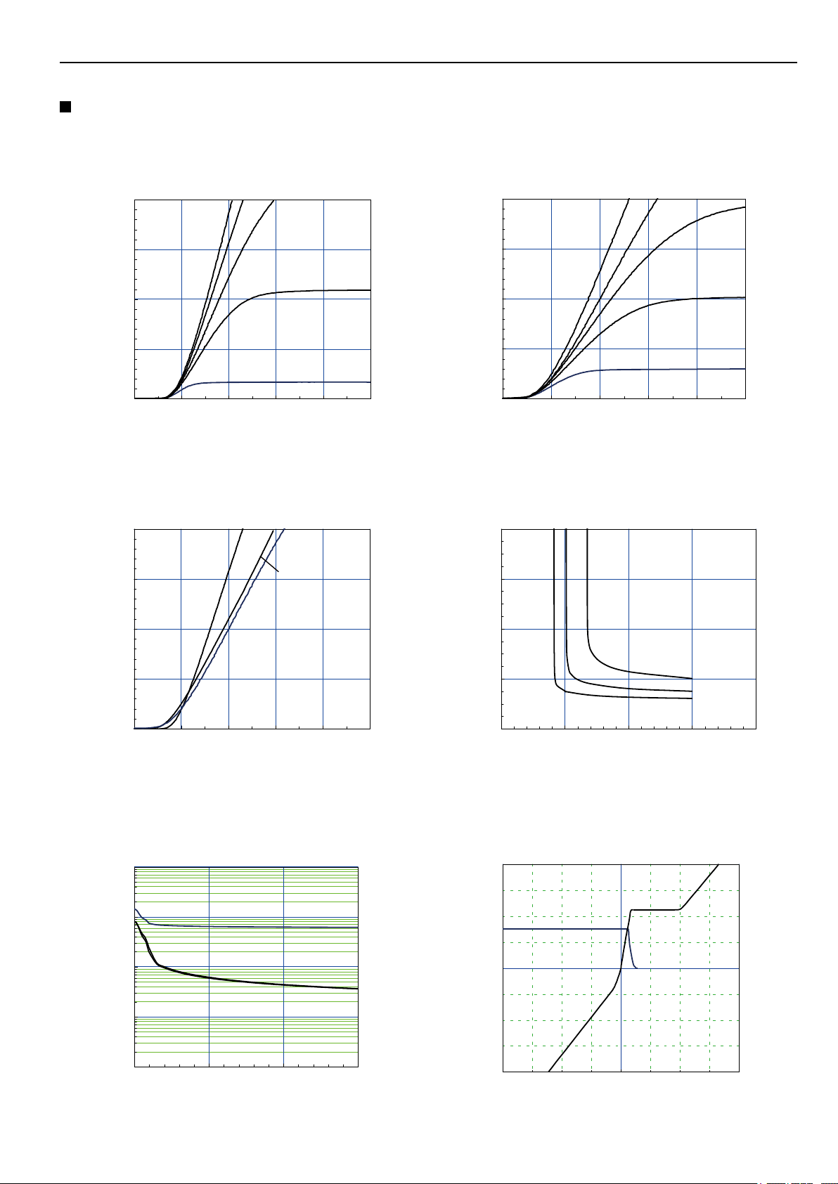
[ Inverter ]
Collector current vs. Collector-Emitter voltage (typ.)
j= 25°C / chip
T
200
V
GE=20V
15V
150
100
50
Collector current: IC [A]
0
0 1 2 3 4 5
Collector-Emitter voltage: VCE[V]
[ Inverter ]
Collector current vs. Collector-Emitter voltage (typ.)
GE=15V / chip
V
200
150
T
j=25°C
Tj=150°C
j=125°C
T
10V
V
[ Inverter ]
Collector current vs. Collector-Emitter voltage (typ.)
T
j= 150°C / chip
200
V
GE=20V
15V
12V
150
100
50
Collector current: IC [A]
V
1
8V
0
0 1 2 3 4 5
Collector-Emitter voltage: V
CE [V]
[ Inverter ]
Collector-Emitter voltage vs. Gate-Emitter voltage (typ.)
T
j= 25°C / chip
8
CE [V]
6
100
50
Collector current: IC [A]
0
0 1 2 3 4 5
Collector-Emitter voltage: V
CE [V]
[ Inverter ]
Capacitance vs. Collector-Emitter voltage (typ.)
V
GE=0V, f= 1MHz, Tj= 25°C
100.0
C
ies
10.0
1.0
0.1
Cres
Coes
4
2
I
I
I
Collector - Emitter voltage: V
0
5 10 15 20 25
Gate - Emitter voltage: VGE [V]
[ Inverter ]
Dynamic gate charge (typ.)
V
CC=300V, IC=100A,Tj= 25°C
VGE
GE [5V/div]
VCE
0
C=200A
C=100A
C=50A
Capacitance: Cies, Coes, Cres [nF]
0.0
0 10 20 30
Collector - Emitter voltage: V
CE [V]
Gate - Emitter voltage: V
Collector - Emitter voltage: VCE [200V/div]
0 800
Gate charge: Qg [nC]
3
Page 4

7MBR100VB060-50
5
r
IGBT Modules
http://www.fujielectric.com/products/semiconductor/
Switching time : ton, tr, toff, tf [ nsec ]
[ Inverter ]
Switching time vs. Collector current (typ.)
CC=300V, VGE=±15V, RG=13Ω, Tj= 125°C
V
10000
1000
off
t
tr
100
10
0 100 200 300
Collector current: IC [A]
[ Inverter ]
Switching time vs. gate resistance (typ.)
CC=300V, IC=100A, VGE=±15V, Tj= 125°C
V
10000
1000
[ Inverter ]
Switching time vs. Collector current (typ.)
CC=300V, VGE=±15V, RG=13Ω, Tj= 150°C
V
10000
ton
1000
toff
ton
t
100
tf
tf
Switching time : ton, tr, toff, tf [ nsec ]
10
0 100 200 300
Collector current: I
C [A]
[ Inverter ]
Switching loss vs. Collector current (typ.)
CC=300V, VGE=±15V, RG=13Ω
V
15
toff
ton
t
r
10
on(150°C)
E
E
on(125°C)
on, Eoff, Err [mJ/pulse ]
100
tf
5
off(125°C)
E
E
rr(150°C)
Err(125°C)
Eoff(150°C)
Switching time : ton, tr, toff, tf [ nsec ]
10
1 10 100 1000
Gate resistance : R
G [Ω]
[ Inverter ]
Switching loss vs. gate resistance (typ.)
VCC=300V, IC=100A, VGE=±15V
30
E
E
20
on(150°C)
on(125°C)
0
Switching loss : E
0 100 200 300
Collector current: IC [A]
[ Inverter ]
Reverse bias safe operating area (max.)
GE=15V, -VGE <= 15V, RG >= 13Ω ,Tj =150°C
+V
300
200
RBSOA
10
E
off(150°C)
E
off(125°C)
100
(Repetitive pulse)
Collector current: IC [A]
E
rr(150°C)
E
0
Switching loss : Eon, Eoff, Err [mJ/pulse ]
1 10 100 1000
Gate resistance : RG [Ω]
rr(125°C)
0
0 200 400 600 800
Collector-Emitter voltage : VCE [V]
(Main terminals)
4
Page 5

7MBR100VB060-50
IGBT Modules
http://www.fujielectric.com/products/semiconductor/
[ Inverter ]
Forward current vs. forward on voltage (typ.)
chip
200
150
100
Tj=150°C
50
Forward current : IF [A]
Tj=125°C
Tj=25°C
0
0.0 0.5 1.0 1.5 2.0 2.5 3.0
Forward on voltage : VF [V]
[ Converter ]
Forward current vs. forward on voltage (typ.)
chip
200
[ Inverter ]
Reverse recovery characteristics (typ.)
V
CC=300V, VGE=±15V, RG=13Ω
1000
rr [ nsec ]
100
Reverse recovery current : Irr [ A ]
Reverse recovery time : t
10
0 100 200 300
Forward current : I
F [A]
t
rr(150°C)
trr(125°C)
Irr(150°C)
I
rr(125°C)
150
100
T
T
50
Forward current : IF [A]
j=125°
j=25°C
0
0.0 0.5 1.0 1.5 2.0 2.5 3.0
Forward on voltage : V
FM [V]
Transient thermal resistance (max.)
1.00
IGBT[Brake]
0.10
n 1 2 3 4
[sec] 0.0023 0.0301 0.0598 0.0708
n
T
IGBT 0.04827 0.12238 0.17288 0.10648
n
r
[°C/W] FWD 0.08581 0.21756 0.30734 0.18929
B-IGBT 0.07616 0.19308 0.27277 0.16800
Thermal resistanse : Rth(j-c) [ °C/W ]
0.01
Conv 0.07079 0.17948 0.25356 0.15617
4
=
1
n
1
=
n
0.001 0.010 0.100 1.000
Pulse width : Pw [sec]
FWD[Inverter]
Conv. Diode
IGBT[Inverter]
t
n
erZth
[ Thermistor ]
Temperature characteristic (typ.)
100
10
1
Resistance : R [kΩ]
0.1
-60 -40 -20 0 20 40 60 80 100 120 140 160 180
Temperature [°C ]
5
Page 6

7MBR100VB060-50
7
0
IGBT Modules
http://www.fujielectric.com/products/semiconductor/
[ Brake ]
Collector current vs. Collector-Emitter voltage (typ.)
j= 25°C / chip
T
100
GE
V
=20V 15V
12V
75
50
25
Collector current: IC [A]
0
0 1 2 3 4 5
Collector-Emitter voltage: VCE [V]
[ Brake ]
Collector current vs. Collector-Emitter voltage (typ.)
GE=15V / chip
V
100
75
T
j=25°C
Tj=150°C
j=125°C
T
10V
[ Brake ]
Collector current vs. Collector-Emitter voltage (typ.)
j= 150°C / chip
T
100
V
GE
=20V
15V
12V
75
V
50
25
Collector current: IC [A]
1
8V
0
0 1 2 3 4 5
Collector-Emitter voltage: V
CE [V]
[ Brake ]
Collector-Emitter voltage vs. Gate-Emitter voltage (typ.)
T
j= 25°C / chip
8
CE [V]
6
50
25
Collector current: IC [A]
0
0 1 2 3 4 5
Collector-Emitter voltage: V
[ Brake ]
Capacitance vs. Collector-Emitter voltage (typ.)
V
GE=0V, f= 1MHz, Tj= 25°C
10.0
ies
C
1.0
Coes
Cres
Capacitance: Cies, Coes, Cres [nF]
0.1
0 10 20 30
Collector - Emitter voltage: VCE [V]
CE [V]
4
I
2
C=100A
C=50A
I
I
C=25A
Collector - Emitter voltage: V
0
5 10 15 20 25
Gate - Emitter voltage: V
GE [V]
[ Brake ]
Dynamic gate charge (typ.)
V
CC=300V, IC=50A, Tj= 25°C
GE [5V/div]
VCE
0
Gate - Emitter voltage: V
Collector - Emitter voltage: VCE [200V/div]
-400 0 400
Gate charge: Qg [nC]
VGE
6
Page 7

7MBR100VB060-50
Outline Drawings(Unit:mm)
IGBT Modules
http://www.fujielectric.com/products/semiconductor/
Equivalent Circuit
[ Converter ] [ Brake ] [ Inverter ] [ Thermistor ]
2(S) 3(T)1(R)
21(P)
23(N)
22(P1)
7(B)
14(Gb)
24(N1)
20
(Gu)
19(Eu)
13(Gx)
18
(Gv)
17(Ev)
4(U)
12(Gy) 11(Gz)
5(V)
Weight: 300g(typ.)
16
(Gw)
15(Ew)
98
6(W)
10(En)
7
Page 8

7MBR100VB060-50
IGBT Modules
http://www.fujielectric.com/products/semiconductor/
WARNING
1. This Catalog contains the product specications, characteristics, data, mater ials, and structures as of March 2014.
The contents are subject to change without notice for specication changes or other reasons. When using a product listed in this Catalog, be
sur to obtain the latest specications.
2. All applic ations described in this Catalog exemplif y the use of Fuji's products for your reference only. No right or license, either express or
implied, under any patent, copyright, trade secret or other intellectual property right owned by Fuji Electric Co., Ltd. is (or shall be deemed)
granted. Fuji Electric Co., Ltd. makes no representation or warranty, whether express or implied, relating to the infringement or alleged
infringement of other's intellectual propert y rights which may arise from the use of the applications described herein.
3. Although Fuji Electric Co., Ltd. is enhancing product quality and reliability, a small percentage of semiconductor products may become
faulty. When using Fuji Electr ic semiconductor products in your equipment, you are requested to take adequate safety measures to prevent
the equipment from causing a physical injury, re, or other problem if any of the products become faulty. It is recommended to make your
design failsafe, ame retardant, and free of malfunction.
4. The products introduced in this Catalog are intended for use in the following electronic and electrical equipment which has normal reliability
requirements.
• Computers • OA equipment • Communications equipment (terminal devices) • Measurement equipment
• Machine tools • Audiovisual equipment • Electrical home appliances • Personal equipment • Industrial robots etc.
5. If you need to use a product in this Catalog for equipment requiring higher reliability than normal, such as for the equipment listed below,
it is imperative to contact Fuji Electric Co., Ltd. to obtain prior approval. When using these products for such equipment, take adequate
measures such as a backup system to prevent the equipment from malfunctioning even if a Fuji's product incorporated in the equipment
becomes faulty.
• Transportation equipment (mounted on cars and ships) • Trunk communications equipment
• Trafc-signal control equipment • Gas leakage detectors with an auto -shut-of f feature
• Emergency equipment for responding to disasters and anti -burglar y devices • Safety devices
• Medical equipment
6. Do not use products in this Catalog for the equipment requiring strict reliability such as the following and equivalents to strategic equipment
(without limitation).
• Space equipment • Aeronautic equipment • Nuclear control equipment
• Submarine repeater equipment
7. Copyright ©1996-2014 by Fuji Electric Co., Ltd. All rights reserved.
No part of this Catalog may be reproduced in any form or by any means without the express permission of Fuji Electr ic Co., Ltd.
8. If you have any question about any por tion in this Catalog, ask Fuji Electric Co., Ltd. or its sales agents before using the product.
Neither Fuji Electric Co., Ltd. nor its agents shall be liable for any injury caused by any use of the products not in accordanc e with instruc tions
set forth herein.
8
Page 9

Technical Information
Please refer to URLs below for futher information about products, application manuals and technical documents.
关于本规格书中没有记载的产品信息,应用手册,技术资料等,请参考以下链接。
本データシートに記載されていない製品情報 , アプリケーションマニュアル , 技術資料は以下の URL をご参照下さい。
IGBT Modules
FUJI ELECTRIC Power Semiconductor WEB site
日本
Global
中国
Europe
North America
www.fujielectric.co.jp/products/semiconductor/
www.fujielectric.com/products/semiconductor/
www.fujielectric.com.cn/products/semiconductor/
www.fujielectric-europe.com/components/semiconductors/
www.americas.fujielectric.com/components/semiconductors/
Information
日本
1
半導体総合カタログ
2
製品情報
3
アプリケーションマニュアル
4
技術資料
5
マウンティングインストラクション
6
IGBT 損失シミュレーションソフト
7
AT-NPC 3-Level 損失シュミレーションソフト
8
富士電機技報
9
製品のお問い合わせ
10
改廃のお知らせ
Global
1
Semiconductors General Catalog
2
Product Information
3
Application Manuals
4
Technical Documents
5
Mounting Instructions
6
IGBT Loss Simulation Software
7
AT-NPC 3-Level Loss Simulation Software www.fujielectric.com/products/semiconductor/model/igbt/simulation_3level/
8
Fuji Electric Journal
9
Contact
10
Revised and discontinued product information www.fujielectric.com/products/semiconductor/discontinued/
www.fujielectric.co.jp/products/semiconductor/catalog/
www.fujielectric.co.jp/products/semiconductor/model/
www.fujielectric.co.jp/products/semiconductor/model/igbt/application/
www.fujielectric.co.jp/products/semiconductor/model/igbt/technical/
www.fujielectric.co.jp/products/semiconductor/model/igbt/mounting/
www.fujielectric.co.jp/products/semiconductor/model/igbt/simulation/
www.fujielectric.co.jp/products/semiconductor/model/igbt/simulation_3level/
www.fujielectric.co.jp/products/semiconductor/journal/
www.fujielectric.co.jp/products/semiconductor/contact/
www.fujielectric.co.jp/products/semiconductor/discontinued/
www.fujielectric.com/products/semiconductor/catalog/
www.fujielectric.com/products/semiconductor/model/
www.fujielectric.com/products/semiconductor/model/igbt/application/
www.fujielectric.com/products/semiconductor/model/igbt/technical/
www.fujielectric.com/products/semiconductor/model/igbt/mounting/
www.fujielectric.com/products/semiconductor/model/igbt/simulation/
www.fujielectric.com/products/semiconductor/journal/
www.fujielectric.com/products/semiconductor/contact/
中国
1
半导体综合目录
2
产品信息
3
应用手册
4
技术资料
5
安装说明书
6
IGBT 损耗模拟软件
7
AT-NPC 3-Level 损耗模拟软件
8
富士电机技报
9
产品咨询
10
产品更改和停产信息
www.fujielectric.com.cn/products/semiconductor/catalog/
www.fujielectric.com.cn/products/semiconductor/model/
www.fujielectric.com.cn/products/semiconductor/model/igbt/application/
www.fujielectric.com.cn/products/semiconductor/model/igbt/technical/
www.fujielectric.com.cn/products/semiconductor/model/igbt/mounting/
www.fujielectric.com.cn/products/semiconductor/model/igbt/simulation/
www.fujielectric.com.cn/products/semiconductor/model/igbt/simulation_3level/
www.fujielectric.com.cn/products/semiconductor/journal/
www.fujielectric.com.cn/products/semiconductor/contact/
www.fujielectric.com.cn/products/semiconductor/discontinued/
2015-10
 Loading...