

Page 1
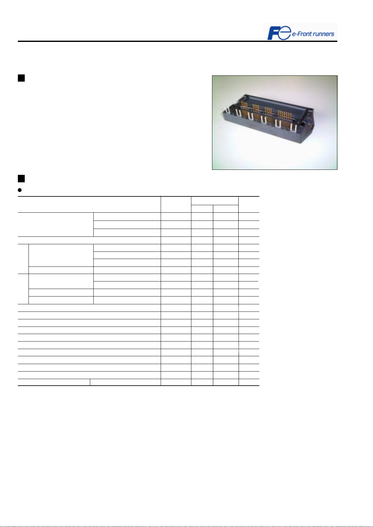
7MBP75TEA120
Econo IPM series
Features
· T emperature protection provided by directly detecting the junction
temperature of the IGBTs
· Low power loss and soft switching
· High performance and high reliability IGBT with overheating protection
· Higher reliability because of a big decrease in number of parts in
built-in control circuit
Maximum ratings and characteristics
Absolute maximum ratings(at Tc=25°C unless otherwise specified)
Item
Bus voltage DC
Surge
Short operating
Collector-Emitter voltage *1
Collector current DC
1ms
DC
Collector power dissipation One transistor *3
Collector current DC
1ms
Forward current diode
Collector power dissipation One transistor *3
Brake Inverter
Supply voltage of Pre-Driver *4
Input signal voltage *5
Input signal current
Alarm signal voltage *6
Alarm signal current *7
Junction temperature
Operating case temperature
Storage temperature
Solder temperature *8
Isolating voltage (Terminal to base, 50/60Hz sine wave 1min.)
Screw torque Mounting (M5)
Symbol Rating Unit
VDC
VDC(surge)
VSC
VCES
IC
ICP
-IC
PC
IC
ICP
IF
PC
VCC
Vin
Iin
VALM
IALM
Tj
Topr
Tstg
Tsol
Viso
0
0
400
0
-
-
-
-
-
-
-
-
-0.5
-0.5
-
-0.5
-
-
-20
-40
-
-
-
1200V / 75A 7 in one-package
Min. Max.
900
1000
800
1200
75
150
75
368
25
50
25
212
20
Vcc+0.5
3
Vcc
20
150
100
125
260
AC2500
3.5
V
V
V
V
A
A
A
W
A
A
A
W
V
V
mA
V
mA
°C
°C
°C
°C
V
N·m
Note
*1 : Vces shall be applied to the input voltage between terminal P and U or ‚V or W or DB, N and U or V or W or DB
*2 : 125
°C/FWD Rth(j-c)/(Ic x VF MAX)=125/0.61/(75 x 2.0) x 100>100%
*3 : Pc=125°C/IGBT Rth(j-c)=125/0.34=368W [Inverter]
Pc=125
°C/IGBT Rth(j-c)=125/0.59=212W [Brake]
*4 : VCC shall be applied to the input voltage between terminal No.4 and 1, 8 and 5, 12 and 9, 14 and 13
*5 : Vin shall be applied to the input voltage between terminal No.3 and 1, 7 and 5, 1 1 and 9, 16,17,18 and 13.
*6 :VALM shall be applied to the voltage between terminal No.2 and 1, No6 and 5, No10 and 9, No.19 and 13.
*7 : IALMshall be applied to the input current to terminal No.2,6,10 and 19.
*8 : Immersion time 10
±1sec.
Page 2

7MBP75TEA120
Electrical characteristics (at Tc=Tj=25°C, Vcc=15V unless otherwise specified.)
Main circuit
Collector current at off signal input
Collector-Emitter saturation voltage
Forward voltage of FWD
Inverter
Collector current at off signal input
Collector-Emitter saturation voltage
Forward voltage of Diode
Brake
Turn-on time
Turn-off time
Reverse recovery time
Control circuit
Supply current of P-line side pre-driver(one unit)
Supply current of N-line side pre-driver
Input signal threshold voltage (on/off)
Input zener voltage
Alarm signal hold time
Current limit resistor
Item Symbol Condition Min. Typ. Max. Unit
ICES
VCE(sat)
VF
ICES
VCE(sat)
VF
ton VDC=600V,Tj=125°C
toff IC=75A Fig.1, Fig.6
trr VDC=600V, IF=75A Fig.1, Fig.6
Item Symbol Condition Min. Typ. Max. Unit
Iccp
ICCN
Vin(th)
VZ
tALM
RALM
VCE=1200V Vin terminal open.
Ic=75A
-Ic=75A
VCE=1200V Vin terminal open.
Ic=25A
-Ic=25A
Switching Frequency : 0 to 15kHz
Tc=-20 to 125°C Fig.7
ON
OFF
Rin=20k ohm
Tc=-20°C Fig.2
T c=25°C Fig.2
T c=125°C Fig.2
Alarm terminal
T erminal
Chip
T erminal
Chip
T erminal
Chip
T erminal
Chip
IGBT-IPM
- - 1.0 mA
- - 3.1 V
- 2.2 -
- - 2.0 V
- 1.6 -
- - 1.0 mA
- - 2.6 V
- 1.9 -
- - 3.7 V
- 2.3 -
1.2 - - µs
- - 3.6
- - 0.3
-
-
1.00
1.25
-
1.1
-
1425
-
-
1.35
1.60
8.0
-
2.0
1500
15
45
1.70
1.95
-
-
-
4.0
1575
ohm
mA
mA
V
V
V
ms
ms
ms
Protection Section ( Vcc=15V)
Item Symbol Condition Min. Typ. Max. Unit
Over Current Protection Level of Inverter circuit
Over Current Protection Level of Brake circuit
Over Current Protection Delay time
SC Protection Delay time
IGBT Chip Over Heating
Protection Temperature Level
Over Heating Protection Hysteresis
Under Voltage Protection Level
Under Voltage Protection Hysteresis
IOC
IOC
tDOC
tSC
TjOH
TjH
VUV
VH
Tj=125°C
Tj=125°C
Tj=125°C
Tj=125°C Fig.4
Surface of IGBT chips
113 - 38 - -
-5-
--8
150 - -
-20 11 .0 - 12.5
0.2 0.5 -
Thermal characteristics( Tc=25°C)
Item Symbol Min. Typ. Max. Unit
Junction to Case thermal resistance *9
Case to fin thermal resistance with compound
*9 For 1device, Case is under the device
Inverter IGBT
FWD
Brake IGBT
Rth(j-c)
Rth(j-c)
Rth(j-c)
Rth(c-f)
- - 0.34
- - 0.61
- - 0.59
- 0.05 -
Noise Immunity ( VDC=300V , Vcc=15V, Test Circuit Fig.5)
Item Condition Min. Typ. Max. Unit
Common mode rectangular noise
Common mode lightning surge
Pulse width 1µs, polarity ±,10minuets
Judge : no over-current, no miss operating
Rise time 1.2µs, Fall time 50µs
Interval 20s, 10 times
Judge : no over-current, no miss operating
±2.0 - -
±5.0 - -
Recommendable value
Item Symbol Min. Typ. Max. Unit
DC Bus Voltage
Operating Supply Voltage of Pre-Driver
Screw torque (M5)
VDC
VCC
-
- - 800 V
13.5 15.0 16.5 V
2.5 - 3.0 Nm
Weight
Item Symbol Min. Typ. Max. Unit
Weight Wt - 270 - g
A
A
µs
µs
°C
°C
V
V
°C/W
°C/W
°C/W
°C/W
kV
kV
Page 3
7MBP75TEA120 IGBT-IPM
Vin(th)
/Vin
/Vin
/ALM
/ALM
Vin(th)
90%
90%
ton
ton
trr
trr
On
On
90%
90%
50%
50%
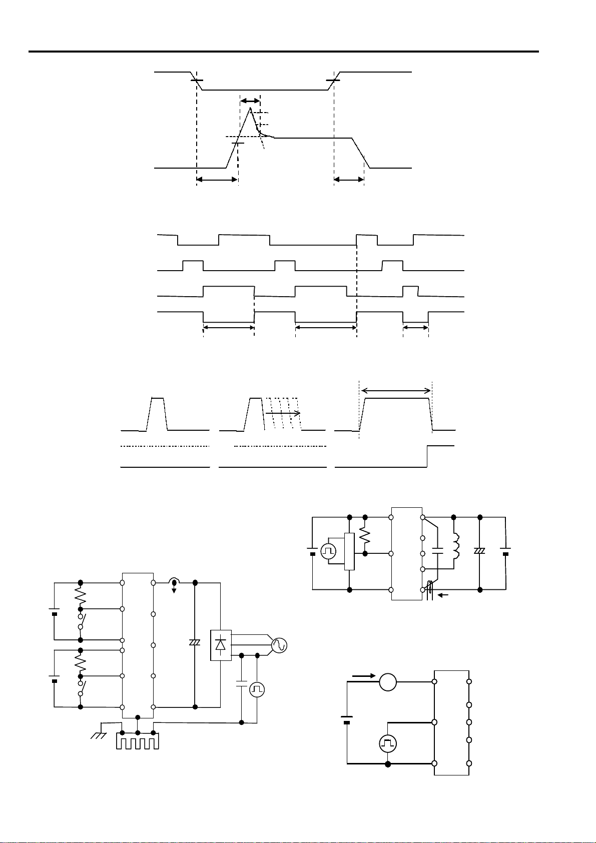
Figure 1. Switching Time Waveform Definitions
off
off
on
on
t
t
ALM >
ALM >
Gate On
Gate On
normal
normal
on
on
Gate Off
Gate Off
alarm
alarm
t
t
ALM >
ALM >
123
123
Fault : O ver-current, Over -heat or Un der- volt age
Fault : O ver-current, Over -heat or Un der- volt age
Figure 2. Input/Output Timing Diagram
Max.
Max.
Vin(th)
Vin(th)
toff
toff
off
off
10%
10%
tsc
tsc
t
t
ALMMax.
ALMMax.
2ms (typ.)
2ms (typ.)
Vin
Vin
Ic
Ic
Vge(Inside IPM )
Vge(Inside IPM )
Fault (Inside IPM )
Fault (Inside IPM )
DC
DC
15V
15V
DC
DC
15V
15V
SW1
SW1
SW2
SW2
Earth
Earth
VccU
VccU
20k
20k
GNDU
GNDU
20k
20k
VinU
VinU
Vcc
Vcc
VinX
VinX
GND
GND
Ic
Ic
I
I
ALM
ALM
IPM
IPM
CT
CT
P
P
U
U
V
V
W
W
N
N
Cooling
Cooling
Fin
Fin
Ic
Ic
ALM
ALM
I
I
Figure.4 Definition of tsc
AC200V
AC200V
+
+
4700p
4700p
AC400V
Noise
Noise
Ic
Ic
ALM
ALM
I
I
Vcc
DC
DC
15V
15V
HCPL-
HCPL4504
4504
Vcc
20k
20k
Vin
Vin
-
-
GND
GND
IPM
IPM
IPM
IPM
P
P
P
P
N
N
N
N
L
L
+
+
+
+
Ic
Ic
Figure 6. Switching Characteristics Test Circuit
Icc
DC
DC
15V
15V
Icc
P.G
P.G
+8V
+8V
fsw
fsw
A
A
Vcc
Vcc
Vin
Vin
GND
GND
IPM
IPM
P
P
U
U
V
V
W
W
N
N
DC
DC
300V
300V
600V
Figure 5. Noise Test Circuit
Figure 7. Icc Test Circuit
Page 4

7MBP75TEA120 IGBT-IPM
Block diagram
P
VccU
VccU
VinU
VinU
ALMU
ALMU
GNDU
GNDU
VccV
VccV
VinV
VinV
ALMV
ALMV
GNDV
GNDV
VccW
VccW
VinW
VinW
ALMW
ALMW
GNDW
GNDW
Vcc
Vcc
VinX
VinX
GND
GND
VinY
VinY
4
44
3
3
2
2
ALM
ALM
R
R
1.5k
1.5k
1
1
8
8
7
7
6
6
ALM
ALM
R
R
1.5k
1.5k
5
5
12
12
11
11
10
10
ALM
ALM
1.5k
1.5k
R
R
9
9
14
14
16
16
13
13
17
17
Pre-Driver
Pre-DriverPre-Driver
Pre-Driver
Pre-DriverPre-Driver
Vz
Vz
Pre-Driver
Pre-DriverPre-Driver
Pre-Driver
Pre-DriverPre-Driver
Vz
Vz
Pre-Driver
Pre-DriverPre-Driver
Pre-Driver
Pre-DriverPre-Driver
Vz
Vz
Pre-Driver
Pre-DriverPre-Driver
Pre-Driver
Pre-DriverPre-Driver
Vz
Vz
Pre-Driver
Pre-DriverPre-Driver
Pre-Driver
Pre-DriverPre-Driver
Vz
Vz
P
U
U
V
V
W
W
VinZ
VinZ
18
18
VinDB
VinDB
15
15
ALM
ALM
19
19
ALM
ALM
R
R
1.5k
1.5k
Outline drawings, mm
Package Type : P622
Pre-DriverPre-Driver
Vz
Vz
B
B
Pre-Driver
Pre-DriverPre-Driver
Pre-Driver
Pre-DriverPre-Driver
Vz
Vz
N
N
1.Amplifier for driver
2.Short circuit protection
3.Under voltage lockout circuit
4.Over current protection
5.IGBT chip over heating protection
Pre-Driver
Pre-drivers include following functions
Pre-DriverPre-Driver
Pre-Driver
MBC F M
Mass : 270g
Page 5

7MBP75TEA120
Characteristics
Control circuit characteristics (Representative)
IGBT-IPM
Power supply current vs. Switching fr equency
Tc=125°C (typ.)
50
P-side
40
30
20
10
Power supply current : Icc (mA)
0
0 5 10 15 20 25
N-side
Switching frequency : fsw (kHz)
Vcc=17V
Vcc=15V
Vcc=13V
Vcc=17V
Vcc=15V
Vcc=13V
Under vol tage vs. Junct ion temperatur e ( t y p.)
14
12
10
Input signal thr eshold voltage
vs. Power supply voltage (typ.)
2.5
2
} Vin(off )
1.5
1
: Vin(on),Vin(off) (V)
Input signal threshold voltage
0.5
0
12 13 14 15 16 17 18
Power supply voltage : Vcc (V)
Under volta ge hyste r isis vs. Jnc tio n temper a t ure (t yp. )
1
0.8
} Vin(on)
Tj=25°C
Tj=125°C
8
6
4
Under voltage : VUVT (V)
2
0
20 40 60 80 100 120 140
Junction temperature : Tj (°C)
Alarm hold ti m e v s. Power supply v oltage (typ.)
3
2.5
Tc=100°C
Alarm hold time : tALM (mSec)
2
1.5
1
0.5
Tc=25°C
0.6
0.4
0.2
Unde r vo ltage h ys terisis : VH (V)
0
20 40 60 80 100 120 140
Junction temperature : Tj (°C)
Over heating characteristics
TjOH,TjH vs. Vcc (typ.)
200
TjOH
150
100
OH hysterisis : TjH (°C)
50
Over heating protection : TjOH (°C)
TjH
0
12 13 14 15 16 17 18
Power supply voltage : Vcc (V)
0
12 13 14 15 16 17 18
Power supply voltag e : Vcc (V)
Page 6

7MBP75TEA120 IGBT-IPM
Main circuit characteristics (Representative)
Collector curr ent vs. Collector-Em itter voltage (typ.)
Tj=25°C(Chip)
150
125
100
75
50
Collector Current : Ic (A)
25
0
0 0.5 1 1.5 2 2.5 3 3.5 4
Col le c to r -Em itt e r voltag e : Vc e (V )
Vcc=17V
Vcc=15V
Vcc=13V
Collector current vs. Collector-Emitter voltage (typ.)
Tj=125°C(Chip)
150
125
Vcc=15V
Collector current vs. Collector-Emitter voltage (typ.)
Tj=25°C(Terminal)
150
125
100
75
50
Collector Current : Ic (A)
25
0
0 0.5 1 1.5 2 2.5 3 3.5 4
Col le c to r -Em itt e r voltag e : Vc e (V )
Vcc=17V
Vcc=15V
Vcc=13V
Collector current vs. Collector-Emitter voltage (typ.)
Tj=125°C(Terminal)
150
125
Vcc=15V
100
75
50
Collector Current : Ic (A)
25
0
00.511.522.533.54
Collector-Emitter voltage : Vce (V)
Vcc=17V
Vcc=13V
Forward current vs. Forward voltage (typ.)
(Chip)
150
125
100
75
50
Forward Current : If (A)
25
25°C
125°C
100
75
50
Collector Current : Ic (A)
25
0
0 0.5 1 1.5 2 2.5 3 3.5 4
Col le c to r -Em itt e r voltag e : Vc e (V )
Vcc=17V
Vcc=13V
Forward current vs. Forward volt age (typ.)
(Terminal)
150
125
100
75
50
Forward Current : If (A)
25
25°C
125°C
0
0 0.5 1 1.5 2 2.5
Forward voltage : Vf (V)
0
0 0.5 1 1.5 2 2.5
Forward voltage : Vf (V)
Page 7

7MBP75TEA120
IGBT-IPM
Switching Loss vs. Collector Current (typ.)
C
35
Edc=600V,Vcc=15V ,Tj=25
30
25
20
15
10
5
Switching loss : E on,Eoff,Err (m J /cyc le)
0
0 25 50 75 100 125
Collector curr ent : Ic (A )
Reversed biased safe operating area
700
600
500
Vcc=15 V,T j<=1 25° C( m in.)
°
Eon
Eoff
Err
Switching Loss vs. Collector Current (typ.)
Edc=600V,Vcc=15V,Tj=125°C
35
30
25
20
15
10
5
Switching loss : Eon,Eo ff,Err (mJ/cycle)
0
0 255075100125
Collector current : Ic (A)
Transient thermal resistance (max.)
1
Eon
Eoff
Err
FW D
400
SCSOA
300
Collector current : Ic (A)
200
100
0
0 200 400 600 800 1 000 1200 1400
(non-r epetitive pulse)
RBSOA
(Re pe titive pulse)
Collector-Emitter voltage : Vce (V)
Power derating for IGBT (max.)
(per device)
500
400
300
200
IGBT
0.1
Thermal resistance : Rth(j-c) (°C/W )
0.01
0.001 0.01 0.1 1
Pulse width :Pw (sec)
Power derating for FWD (max.)
(per device)
250
200
150
100
100
Collecter Power Diss ipa ti o n : Pc (W)
0
0 20 40 60 80 100 120 140 160
Case Temperature : Tc (°C)
50
Collecter Power Dissipation : Pc (W)
0
0 20 40 60 80 100 120 140 160
Case Temperature : Tc (°C)
Page 8

7MBP75TEA120 IGBT-IPM
Sw itc hin g ti m e v s. C o ll ec tor cur ren t (ty p. )
Edc=600V,Vcc=15V,Tj=25
10000
1000
100
Switching time : ton,toff,tf (nSec)
10
0 20 40 60 80 100 1 20 140
Collector current : Ic (A)
Reverse recovery characteristics (typ.)
trr,Irr vs.IF
C
°
toff
ton
tf
trr125°C
Sw itc h in g ti m e v s . Co lle c tor cu rren t (ty p. )
Edc=600V,Vcc=15V,Tj=125°C
10000
1000
100
Switching time : ton,toff,tf (nSec)
10
0 20406080100120140
Collector current : Ic (A)
toff
ton
tf
100
trr25°C
Irr125°C
Irr25°C
10
Reverse recovery current:Irr(A)
Reverse recovery time:trr(nsec)
1
0 20 40 60 80 100 120 140
Forward current:IF(A)
Page 9

7MBP75TEA120 IGBT-IPM
Characteristics
Dynamic Brake Characteristics (Representative)
Collector curr ent vs. Collector-Em itter voltage (typ.)
Tj=25°C
80
60
Vcc=17V
40
Collector Current : Ic (A)
20
0
00.511.522.533.5
Col le c to r -Em itt e r voltag e : Vc e (V )
Transient thermal resistance (max.)
1
Vcc=15V
Vcc=13V
IGB T
Collector curr ent vs. Collector-Em itter voltage (typ.)
Tj=125°C
80
60
Vcc=17V
40
Collector Current : Ic (A)
20
0
00.511.522.533.5
Col le c to r -Em itt e r voltag e : Vc e (V )
Reversed biased safe operating area
350
300
Vcc=15V,Tj<=125°C (min.)
Vcc=15V
Vcc=13V
0.1
Therm al r esistance : Rth(j-c ) (°C /W )
0.01
0.001 0.01 0.1 1
Pulse width :Pw (sec)
Power derating for IGBT (max.)
(per device)
250
200
150
100
250
200
150
Collector current : Ic (A)
100
50
0
0 200 400 600 800 1000 1200 1400
SCSOA
(non-repetitive pulse)
RBSOA
(R epetitive p u ls e )
Collector-Emitter voltage : Vce (V)
50
Collecter Power Diss ipa ti o n : Pc (W)
0
0 20 40 60 80 100 120 140 160
Case Temperature : Tc (°C)
 Loading...