

Page 1
SPECIFICATION
Device Name :
Type Name :
Spec. No. :
IGBT - IPM
7MBP75RTB060
MS6M 0653
Sep. 17 '02
Sep. 17 '02
Sep.-17 -'02
K.Sekigawa
Nishiura
K.Yamada
T.Fujihira
Fuji Electric Co.,Ltd.
Matsumoto Factory
MS6M 0653
a
1
23
H04-004-07
Page 2
R e v i s e d R e c o r d s
Date
Sep.-17-'02
Apr.-09-'03
Classi-
fication Ind. Content
enactment
a
Revision
Reliability Test Items.
Applied
date Drawn Checked Approved
Issued
date
Apr.-09-'03
Nishiura
K.Yamada
T.Miyasaka
K.Yamada
T.FujihiraK.Sekigawa
T.FujihiraN.Matsuda
MS6M 0653
2
a
22
H04-004-06
Page 3
7MBP75RTB060
1. Outline Drawing ( Unit : mm )
Package type : P610
±0.3
±0.3±0.3
±0.3
2
22
2
20
2020
2020
±1
±1±1
±1
±0.3
±0.3±0.3
±0.3
88
8888
88
74
7474
74
10
1010
10
2020
2017
1717
17
0.5
0.50.5
0.5
13.8
13.8
13.813.8
3.22
3.22
3.223.22
a
±0.3
±0.3
±0.3±0.3
±0.2
±0.2 ±0.2
±0.2±0.2
10.16
10.16 10.16
10.1610.16
±0.3
±0.3
±0.3±0.3
±0.15
±0.15 ±0.15
±0.15±0.15
5.08
5.08
5.085.08
11114
5.08
5.085.08
47
44
B
P
N
W
±1
±1
±1±1
109
109
109109
±0.3
±0.3
±0.3±0.3
95
95
9595
67.4
67.4
67.467.4
±0.2 ±0.2
±0.2±0.2
10.16
10.16
10.1610.16
10.16
10.1610.16
±0.15 ±0.15
±0.15±0.15
±0.15
±0.15±0.15
5.08
5.085.08
5.085.08
710
77
V
±0.2 ±0.25
±0.2±0.2
10 16
1010
15.24
15.24
15.2415.24
2.54
2.54
2.542.54
±0.25
±0.25±0.25
±0.1
±0.1
±0.1±0.1
16
1616
U
4-φ
4-φ
5.5
5.5
4-φ4-φ
5.5 5.5
+1.0
+1.0+1.0
+1.0
-0.3
-0.3-0.3
-0.3
22
2222
22
+1.0
+1.0+1.0
+1.0
-0.2
-0.2-0.2
-0.2
8
88
8
6-M5
3.22
3.223.22
φφφφ
0.5
0.50.5
±0.3
±0.3
±0.3±0.3
2.5
2.5
2.52.5
( φ 1 ~ 1.5)
(1~ 2)
24
24 26
2424
Lot No.
Indication of Lot No.
±0.1
±0.1
±0.1±0.1
2.54
2.54 2.54
2.542.54
2.543.22
2.542.54
2222 22222222
□ 0.64
26 26
2626
±0.1
±0.1
±0.1±0.1
4.5
4.54.5
4.5
10
1010
10
±0.3
±0.3
±0.3±0.3
8
88
8
1
11
1
260.5
2626
16-
16- 2-φ
16-16-
2-φ
0.64
0.64 2.5
0.640.64
2.5
2-φ2-φ
2.52.5
Odered No. in monthly
Manufactured month
(Jan.~Sep.:1~9,Oct.:O,Nov.:N,Dec.:D)
Last digit of manufactured year
0.1max
0.1max0.1max
0.1max
14.5
14.514.5
14.5
7
77
7
17
1717
17
+1.0
+1.0+1.0
+1.0
9
99
9
-0.3
-0.3-0.3
-0.3
22
2222
22
31
3131
31
Details of control terminals
Dimensions in mm
MS6M 0653
3
a
23
H04-004-03
Page 4
2.Pin Descriptions
Main circuit
Control circuit
Symbol
P
U
V
W
N
B
№ Symbol Description
① GNDU High side ground (U).
② VinU Logic input for IGBT gate drive (U).
③ VccU High side supply voltage (U).
④ GNDV High side ground (V).
Positive input supply voltage.
Output (U).
Output (V).
Output (W).
Negative input supply voltage.
Collector terminal of Brake IGBT.
Description
⑤ VinV Logic input for IGBT gate drive (V).
⑥ VccV High side supply voltage (V).
⑦ GNDW High side ground (W).
⑧ VinW Logic input for IGBT gate drive (W).
⑨ VccW High side supply voltage (W).
⑩ GND Low side ground.
⑪ Vcc Low side supply voltage.
⑫ VinDB Logic input for Brake IGBT gate drive.
⑬ VinX Logic input for IGBT gate drive (X).
⑭ VinY Logic input for IGBT gate drive (Y).
⑮ VinZ Logic input for IGBT gate drive (Z).
⑯ ALM Low side alarm signal output.
MS6M 0653
a
4
23
H04-004-03
Page 5
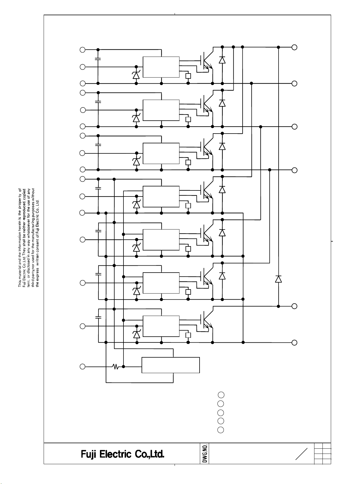
3. Block Diagram
3
cV
3
2
2
1
1
6
6
5
5
4
4
9
9
8
8
7
7
11
11
VccU
VccU
VinU
VinU
VinU
GNDU
GNDU
GNDU
VccV
VccV
VinV
VinV
VinV
GNDV
GNDV
GNDV
VccW
VccW
VccW
VinW
VinW
VinW
GNDW
GNDW
GNDW
Vcc
Vcc
Vcc
P
P
Pre-Driver
Pre-Driver
Pre-Driver
V
V
V
Z
Z
Z
U
U
Pre-Driver
Pre-Driver
Pre-Driver
V
V
V
Z
Z
Z
V
V
Pre-Driver
Pre-Driver
Pre-Driver
V
V
V
Z
Z
Z
W
W
VinX
VinX
VinX
GND
GND
GND
VinY
VinY
VinY
VinZ
VinZ
VinZ
VinDB
VinDB
VinDB
ALM
ALM
ALM
Pre-Driver
Pre-Driver
13
13
V
V
V
10
10
14
14
V
V
V
15
15
V
V
V
12
12
V
V
R
R
ALM
16
16
ALM
1. 5k
1. 5k
1. 5k
Ω
Ω
Ω
Pre-Driver
Z
Z
Z
Pre-Driver
Pre-Driver
Pre-Driver
Z
Z
Z
Pre-Driver
Pre-Driver
Pre-Driver
Z
Z
Z
Pre-Driver
Pre-Driver
Z
Z
Over heating prot ect ion
Over heating prot ect ion
circuit
circuit
B
B
N
N
Pre-drivers include following functions
1 Amplifier for driver
2 Short circuit protection
3 Under voltage lockout circuit
4 Over current protection
5 IGBT chip over heating protection
MS6M 0653
5
H04-004-03
a
23
Page 6
4.Absolute Maximum Ratings
Tc=25℃ unless otherwise specified.
Items
Bus Voltage
(between terminal P and N)
DC
Surge
Shortoperating Vsc 200 400 V
Collector-Emitter Voltage *1
DC Ic - 75 A
Collector Current
Inverter
Collector Power Dissipation One transistor *3 Pc - 198 W
Collector Current
Forward Current of Diode
Brake
Collector Power Dissipation One transistor *3 Pc - 198 W
1ms Icp - 150 A
Duty=75.0 % *2 -Ic - 75 A
DC Ic - 50 A
1ms Icp - 100 A
Supply Voltage of Pre-Driver *4
Input Signal Voltage *5
Input Signal Current
Alarm Signal Voltage *6
Alarm Signal Current *7
Junction Temperature
Operating Case Temperature
Storage Temperature
Isolating Voltage
(Terminal to base, 50/60Hz sine wave 1min.) *8
Screw Torque Terminal (M5)
Mounting (M5)
Symbol Min. Max. Units
V
DC
V
DC(surge)
Vces 0 600 V
IF - 50 A
Vcc -0.5 20 V
Vin -0.5 Vcc+0.5 V
Iin - 3 mA
VALM -0.5 Vcc V
IALM
Tj - 150
Topr -20 100
Tstg -40 125
Viso - AC2500
-
0 450 V
0 500 V
-20mA
℃
℃
℃
V
Nm3.5-
Note
*1 :Vces shall be applied to the input voltage between terminal P and U or V or W or DB, N and U
or V or W or DB
*2 : 125℃/FWD Rth(j-c)/(Ic×VF MAX)=125/0.855/(75×2.6)×100=75.0%
*3 : Pc=125℃/IGBT Rth(j-c)=125/0.63=198W [Inverter]
Pc=125℃/IGBT Rth(j-c)=125/0.63=198W [Break]
*4 : VCC shall be applied to the input voltage between terminal No.3 and 1,6 and 4, 9 and 7,
11 and 10.
*5 : Vin shall be applied to the input voltage between terminal No.2 and 1, 5 and 4, 8 and 7,
13,14,15 and 10.
*6 :
VALM
*7 :
IALM
*8 : 50Hz/60Hz sine wave 1 minute.
shall be applied to the voltage between terminal No.16 and 10.
shall be applied to the input current to terminal No.16.
MS6M 0653
6
a
23
H04-004-03
Page 7
5. Electrical Characteristics
Tj=25℃,Vcc=15V unless ot herwis e specified.
5.1 Main circuit
Item Conditions
Collec tor Current
at off signal input Vin terminal open.
Collec tor-Emitter
InverterBrake
saturation voltage Chip - 2. 0 - V
Forward voltage of FWD
Symbol Min. Typ. Max. Units
600V
=
V
(sat)
CE
75A Terminal - - 2.4
Ic=
-
75A Terminal - - 2.6
Ic=
I
CES
V
CE
--1.0mA
VF
Chip - 1.6 - V
Collec tor Current
I
at off signal input Vin terminal open.
CES
Collec tor-Emitter
V
CE
saturation voltage Chip - 1.75 - V
(sat)
600V
=
V
CE
50A Terminal - - 2.2
Ic=
-
50A Terminal - - 3.3
Ic=
--1.0
mA
Forward voltage of Diode VF
Chip - 1.9 - V
Turn-on time ton V
300V、Tj= 125
=
DC
℃
1.2 - -
Turn-off tim e toff Ic=75A Fig.1,Fig.6 - - 3. 6 us
Reverse recovery time
trr V
DC
=
300V
0.3--
IF=75A Fig.1,Fig.6
V
V
V
V
AV
P
internal wiring
Maximum AvalancheEnergy inductance=50nH 40 - - mJ
(A non-repetit ion)
Main c ircuit wiring
inductance=54nH
5.2 Control c ircuit
Item Conditions
Symbol Min. Typ. Max. Units
Supply c urrent Switching Frequency
of P-side pre-driver (one unit)
Iccp
: 0~15kHz
mA--18
Supply c urrent Iccn Tc=-20~125℃ Fig.7
--65
mA
of N-side pre-driver
ON 1 1.35 1.7
Vin(th)Input signal threshold voltage
V
OFF 1.25 1.6 1.95
Input Zener Voltage Vz Rin=20kΩ -8.0- V
Tc=-20℃ Fig.2 1.1 - -
Alarm Signal Hold Time tALM Tc=25℃ Fig.2 - 2. 0 - ms
Tc=125℃ Fig.2 - - 4.0
Current Limit Resis tor RALM Alarm terminal 1425 1500 1575 Ω
MS6M 0653
7
23
H04-004-03
a
Page 8

5.3 Protection Section (Vcc
=15V)
Item
Over Current Protection Level Tj=125℃ 113 - -
of Inverter circuit Ioc A
Over Current Protection Level Tj=125℃ 75 - -
of Brake circuit
Over Current Protection Delay time tdoc Tj=125℃ -5-us
SC Protection Delay time tsc Tj=125℃ Fig.4 - - 8 us
IGBT Chips Ov er Heating TjOH Surface 150 - -
Protection Temperature Level of IGBT Chips
Over Heating Protection Hysteresis TjH - 20 -
Over Heating Protection TcOH VDC=0V,IC=0A 110 - 125
Temperature Level CaseTemperature
Over Heating Protection Hysteresis TcH - 20 -
Under Voltage Protection Level VUV 11 - 12.5 V
Under Voltage Protection Hysteresis VH 0.2 0.5 -
6. Thermal Characteristics (Tc=25℃)
Symbol Conditions Min. Typ. Max. Units
℃
℃
℃
Item Symbol Min. Typ. Max. Units
Junction to Case Inverter IGBT Rth(j-c) - - 0.63
Thermal Resistance *9 FWD Rth(j-c) - - 0.855 ℃/W
Brake IGBT Rth(j-c) 0.63
Case to Fin Thermal Resistance with Compound Rth(c-f) - 0.05 -
7. Noise Immunity (Vdc=300V、Vcc=15V、Test Circuit Fig 5.
Item Conditions Min. Typ. Max. Units
Common mode Pulse width 1us,polarity ±,10 minuets ±2.0 - - kV
rectangular noise Judge:no ov er-current, no miss operating
Common mode
lightning surge Judge:no over-current, no miss operating
8. Recommended Operating Conditions
Item Symbol Min. Typ. Max. Units
DC Bus Voltage VDC - - 400 V
Power Supply Voltage of Pre-Driver Vcc 13.5 15 16.5 V
Rise time 1.2us,Fall time 50usInterval 20s,10 times
)
±5.0 - - kV
Screw Torque (M5) - 2.5 - 3 Nm
9. W eight
Item Symbol Min. Typ. Max. Units
Weight Wt - 450 - g
*9:( For 1device ,Case is under the dev ice )
MS6M 0653
8
H04-004-03
a
23
Page 9

Vin
Vin(th)
trr
On
Vin(th)
90%
50%
Ic
90%
ton
Figure 1. Switching Time Waveform Definitions
/Vin
Vge (Inside IPM)
Fault (Inside IPM)
/ALM
on
Gate On
normal
off
Gate Off
alarm
t
ALM>Max.
on
t
ALM>Max.
①②③
Fault:Over-current,Over-heat or Under-voltage
Figure 2. Input/Output Timing Diagram
Necessary conditions for alarm reset (refer to ① to ③ in figure2.)
This represents the case when a failure-causing Fault lasts for a period more than tALM.
①
The alarm resets when the input Vin is OFF and the Fault has disappeared.
toff
off
10%
t
ALM
2ms(typ.)
This represents the case when the ON condition of the input Vin lasts for a period more
②
than tALM. The alarm resets when the Vin turns OFF under no Fault conditions.
This represents the case when the Fault disappears and the Vin turns OFF within tALM.
③
The alarm resets after lasting for a period of the specified time tALM.
Period ①:
/Vin
Ic
/ALM
on
Ioc
①
off
<tdoc
on
②
alarm
tdoc
Figure 3. Over-current Protection Timing Diagram
When a collector current over the OC level flows and the OFF command is input within
a period less than the trip delay time tdoc, the current is hard-interrupted and no alarm
is output.
Period ②:
When a collector current over the OC level flows for a period more than the trip delay
time tdoc, the current is soft-interrupted. If this is detected at the lower arm IGBTs,
an alarm is output.
9
MS6M 0653
23
H04-004-03
a
Page 10

t
SC
Ic
I
ALM
DC
15V
DC
15V
SW1
SW2
Ic
I
ALM
Figure.4 Definition of tsc
P
U
V
W
N
20k
20k
Earth
VccU
VinU
GNDU
Vcc
VinX
GND
IPM
CT
Cooling
Fin
Ic
I
ALM
AC200V
+
4700p
Noise
Figure 5. Noise Test Circuit
Vcc
Vcc
20k
DC
DC
15V
15V
HCPL-
HCPL4504
4504
Figure 6. Switching Characteristics Test Circuit
20k
Vin
Vin
GND
GND
Icc
A
DC
15V
P.G
+8V
fsw
IPM
IPM
Vcc
Vin
GND
P
P
L
L
+
+
N
N
Ic
Ic
P
IPM
U
V
W
N
DC
DC
300V
300V
Figure 7. Icc Test Circuit
MS6M 0653
10
a
23
H04-004-03
Page 11

10. Truth table
.
P
10.1 IGBT Control
The following table shows the IGBT ON/OFF status with respect to the input signal Vin
The IGBT turn-on when Vin is at “Low” level under no alarm condition.
Input Output
(Vin) (IGBT)
Low ON
High OFF
10.2 Fault Detection
(1) When a fault is detected at the high side, only the detected arm stops its output.
At that time the IPM dosen’t any alarm.
(2) When a fault is detected at the low side, all the lower arms stop their outputs and the I
outputs an alarm of the low side.
High side
U-phase
High side
V-phase
High side
W-phase
Low side
Case
Fault
IGBT
U-phase V-phase W -phase Low side ALM
OC OFF * * * H
UVOFF*** H
TjOH OFF * * * H
OC * OFF * * H
UV * OFF * * H
TjOH * OFF * * H
OC * * OFF * H
UV * * OFF * H
TjOH * * OFF * H
OC * * * OFF L
UV * * * OFF L
TjOH * * * OFF L
TcOH * * * OFF L
Alarm Output
Temperature
*:Depend on input logic.
MS6M 0653
11
a
23
H04-004-03
Page 12

11. Cautions for design and application
1. Trace routing layout should be designed with particular attention to least stray capacity
between the primary and secondary sides of optical isolators by minimizing the wiring
length between the optical isolators and the IPM input terminals as possible.
フォトカプラとIPMの入力端子間の配線は極力短くし、フォトカプラの一次側と二次側の浮遊容量を小さくした
パターンレイアウトにして下さい。
2. Mount a capacitor between Vcc and GND of each high-speed optical isolator as close to
as possible.
高速フォトカプラの
Vcc-GND
間に、コンデンサを出来るだけ近接して取り付けて下さい。
3. For the high-speed optical isolator, use high-CMR type one with tpHL, tpLH ≦ 0.8µs.
高速フォトカプラは、
tpHL,tpLH≦0.8us、高CMR
タイプをご使用ください。
4. For the alarm output circuit, use low-speed type optical isolators with CTR ≧ 100%.
アラーム出力回路は、低速フォトカプラ
CTR≧100%
のタイプをご使用ください。
5. For the control power Vcc, use four power supplies isolated each. And they should be
designed to reduce the voltage variations.
制御電源
Vcc
は、絶縁された4電源を使用してください。また、電圧変動を抑えた設計として下さい。
6. Suppress surge voltages as possible by reducing the inductance between the DC bus P
and N, and connecting some capacitors between the P and N terminals.
P-N
間の直流母線は出来るだけ低インダクタンス化し、
電圧を低減して下さい。
P-N
端子間にコンデンサを接続するなどしてサージ
7. To prevent noise intrusion from the AC lines, connect a capacitor of some 4700pF between
the three-phase lines each and the ground.
AC
ラインからのノイズ侵入を防ぐために、3相各線-アース間に4700pF程のコンデンサを接続して下さい。
8. At the external circuit, never connect the control terminal ①GNDU to the main terminal
U-phase, ④GNDV to V-phase, ⑦GNDW to W-phase, and ⑩GND to N-phase. Otherwise,
malfunctions may be caused.
制御端子①GNDUと主端子U相、制御端子④GNDVと主端子V相、制御端子⑦GNDWと主端子W相、
制御端子⑩GNDと主端子Nを外部回路で接続しないで下さい。誤動作の原因になります。
9. Take note that an optical isolator’s response to the primary input signal becomes slow
if a capacitor is connected between the input terminal and GND.
入力端子
のでご注意ください。
-GND
間にコンデンサを接続すると、フォトカプラ一次側入力信号に対する応答時間が長くなります
MS6M 0653
12
23
a
H04-004-03
Page 13

10. Taking the used isolator’s CTR into account, design with a sufficient allowance to decide
e
o
a
the primary forward current of the optical isolator.
フォトカプラの一次側電流は、お使いのフォトカプラの
CTR
を考慮し十分に余裕をもった設計にして下さい。
11. Apply thermal compound to the surfaces between the IPM and its heat sink to reduce
the thermal contact resistance.
接触熱抵抗を小さくするために、IPMとヒートシンクの間にサーマルコンパウンドを塗布して下さい。
12. Finish the heat sink surface within roughness of 10µm and flatness (camber) between scr
positions of 0 to +100µm. If the flatness is minus, the heat radiation becomes worse due t
a gap between the heat sink and the IPM. And, if the flatness is over +100µm, there is a d
that the IPM copper base may be deformed and this may cause a dielectric breakdown.
ヒートシンク表面の仕上げは、粗さ
での平坦度(反り)は、0~
イナスの場合、ヒートシンクと
悪化します。また、平坦度が+
ベースが変形し絶縁破壊を起こす危険性があります。
100um
10um
以下、ネジ位置間
として下さい。平坦度がマ
IPM
の間に隙間ができ放熱が
100um
以上の場合IPMの銅
Heat sink
Mounting holes
+100μm
0
13. This product is designed on the assumption that it applies to an inverter use. Sufficient
examination is required when applying to a converter use. Please contact Fuji Electric Co.,
if you would like to applying to converter use.
本製品は、インバータ用途への適用を前提に設計されております。コンバータ用途へ適用される場合は、
十分な検討が必要です。もし、コンバータへ適用される場合は御連絡ください。
14. Please see the 『Fuji IGBT-IPM R SERIES APPLICATION MANUAL』 and 『Fuji IGBT
MODULES N SERIES APPLICATION MANUAL』.
『富士
IGBT-IPM R
シリーズ アプリケーションマニュアル』及び『
IGBT
モジュール Nシリーズ アプリケーション
マニュアル』を御参照ください。
MS6M 0653
13
a
23
H04-004-03
Page 14

12. Example of applied circuit 応用回路例
20kΩ
I
F
Vcc
20kΩ
IF
Vcc
20kΩ
I
F
Vcc
20kΩ
I
F
Vcc
20kΩ
I
F
0.1uF
0.1uF
0.1uF
0.1uF
0.1uF
+
10uF
+
10uF
+
10uF
+
10uF
+
10uF
③
IPM
②
①
⑥
⑤
④
⑨
⑧
⑦
⑪
⑫
⑩
⑬
P
U
V
W
B
N
M
AC200V
+
20kΩ
I
F
20kΩ
I
F
1k
5V
0.1uF
0.1uF
+
10uF
⑭
+
10uF
⑮
⑯
13. Package and Marking 梱包仕様
Please see the MT6M4140 which is packing specification of P610 & P611 & P621 package.
P610,611,621 梱包仕様書 MT6M4140を御参照ください。
14. Cautions for storage and transportation 保管、運搬上の注意
・ Store the modules at the normal temperature and humidity (5 to 35°C, 45 to 75%).
常温常湿(5~35℃、45~
75%)
で保存して下さい。
・ Avoid a sudden change in ambient temperature to prevent condensation on the module
surfaces.
モジュールの表面が結露しないよう、急激な温度変化を避けて下さい。
・ Avoid places where corrosive gas generates or much dust exists.
腐食性ガスの発生場所、粉塵の多い場所は避けて下さい。
・ Store the module terminals under unprocessed conditions
モジュールの端子は未加工の状態で保管すること。
.
・ Avoid physical shock or falls during the transportation.
運搬時に衝撃を与えたり落下させないで下さい。
15. Scope of application 適用範囲
This specification is applied to the IGBT-IPM (type: 7MBP75RTB060).
本仕様書は、IGBT-IPM (型式:7MBP75RTB060)に適用する。
16. Based safety standards 準拠安全規格
UL1557
MS6M 0653
14
a
23
H04-004-03
Page 15

Page 16

Page 17

Page 18

Page 19

Page 20

18.
18.Reliability Test Items
18.18.
Reliability Test Items
Reliability Test ItemsReliability Test Items
a
Test
cate-
Test items Test methods and conditions
gories
1 Terminal strength Pull force : 40 N (main terminal)
端子強度
(Pull test) Test time : 10 ±1 sec.
2 Mounting Strength Screw torque : 2.5 ~ 3.5 N・m (M5)
締付け強度
3 Vibration Range of frequency : 10
振動
4 Shock Maximum ac celeration :
衝撃
Mechanical Tests
Mechanical Tests
5 Solderabitlity Solder temp. : 235 ±5
はんだ付け性
6 Resistance to Solder temp. : 260 ±5
soldering heat Immersion time : 10 ±1sec.
はんだ耐熱性
1 High temperature Storage temp. : 125 ±5
storage
2 Low temperature Storage temp. : -40 ±5
storage
3 Temperature Storage temp. : 85 ±2
humidity storage Relative hum idity : 85 ±5%
高温高湿保存
4 Uns aturated Test temp. : 120 ±2
pressure cooker Atmos pheric pressure :
プレッシャークッ カ ー
5 Temperature Test temp. :
cycle
温度サイクル
Environment Tests
Environment Tests
6 Thermal shock
熱衝撃
高温保存
低温保存
10 N (control terminal)
Test time : 10 ±1 sec.
~500 Hz
Sweeping tim e : 15 min.
Acc eler ation :
100 m/s
2
Sweeping direction : Each X,Y,Z axis
Test time : 6 hr. (2hr./direction)
5000 m/s
2
Pulse width 1.0 ms
Direction : Each X,Y,Z axis
Test time : 3 times/direction
℃
Immersion duration : 5.0 ±0.5 sec.
Test time : 1 time
Each terminal should be Immersed in solder
within 1~1.5mm from the body.
℃
Test time : 1 time
Each terminal should be Immersed in solder
within 1~1.5mm from the body.
℃
Test duration : 1000 hr.
℃
Test duration : 1000 hr.
℃
Test duration : 1000hr.
℃
5
Pa
1.7x10
Test humidity : 85 ±5%
Test duration : 96 hr.
Minimum storage temp. -40 ±5
Maximum storage temp. 125 ±5
Normal temp. 5 ~ 35
Dwell time : Tmin ~ T
N
~ Tmax ~ T
N
1hr. 0.5hr. 1hr. 0.5hr.
Number of cycles : 100 cycles
Test temp. :
High temp. side 100
Low temp. side 0 -0
+0
-5
℃
+5
℃
Fluid us ed : Pure water (running water)
Dipping time : 5 min. par eac h temp.
Trans fer tim e : 10 s ec .
Number of cycles : 10 cycles
℃
℃
℃
Reference
norms
EIAJ
ED-4701
Test Method 401
Method
Ⅰ
Test Method 402
method
Ⅱ
Test Method 403
Condition code B
Test Method 404
Condition code B
Test Method 303
Condition code A
Test Method 302
Condition code A
Test Method 201
Test Method 202
Test Method 103
Test code C
Test Method 103
Test code E
Test Method 105
Test Method 307
method
Ⅰ
Condition code A
Number
of sample
5 ( 1 : 0 )
5 ( 1 : 0 )
5 ( 1 : 0 )
5 ( 1 : 0 )
5 ( 1 : 0 )
5 ( 1 : 0 )
5 ( 1 : 0 )
5 ( 1 : 0 )
5 ( 1 : 0 )
5 ( 1 : 0 )
5 ( 1 : 0 )
5 ( 1 : 0 )
Acc eptance
number
MS6M 0653
20
a
23
H04-004-03
Page 21

a
Test
categories
Endurance TestsEndurance Tests
19.
19.Failure Criteria
19.19.
Test items Test methods and conditions
1 High temperature Test temp. :
revers e bias (Tj
高温逆バイアス
2 Temperature Test temp. : 85 ±2
humidity bias Relative humidity : 85 ±5 %
高温高湿バイアス
3 Intermitted ON time : 2 sec.
operating life OFF tim e : 18 sec .
(Power c ycle) Tes t temp. :
断続動作
Failure Criteria
Failure CriteriaFailure Criteria
Bi as Volt age : VC = 0.8×VCES
Bias Method : Applied DC voltage to C-E
Test duration : 1000 hr.
Bi as Volt age : VC = 0.8×VCES
Bias Method : Applied DC voltage to C-E
Test duration : 1000 hr.
Number of cycles : 15000 cyc les
Reference norms
EIAJ
ED-4701
Ta = 125 ±5
Vcc = 15V
Vcc = 15V
Tj=100 ±5deg
∆
Tj
≦
℃
150 ℃)
≦
℃
150 ℃, Ta=25 ±5
℃
Test Met hod 101
Test Met hod 102
Conditi on code C
Test Met hod 106
Num ber
of sample
Acceptance
number
5 ( 1 : 0 )
5 ( 1 : 0 )
5 ( 1 : 0 )
Item Characteristic Symbol Failure criteria Unit Note
Lower limit Upper limit
Electrical Leakage current ICES - USL×2 mA
characteristic Saturation voltage VCE(sat) - USL×1.2 V
Forward voltage VF - USL×1.2 V
Thermal IGBT
resistance FWD
Rth(j-c)
Rth(j-c)
Over Current Protection Ioc
Alarm signal hold time tALM
Over heating Protection TcOH
-USL×1.2℃/W
-USL×1.2℃/W
LSL×0.8 USL×1.2
LSL×0.8 USL×1.2
LSL×0.8 USL×1.2
A
ms
℃
Isolation voltage Viso Broken insulation -
Visual Visual inspection
inspection Peeling - The visual sample -
Plating
and the others
LSL : Lower specified limit.
USL : Upper specified limit.
Note :
Each parameter measurement read-outs shall be made after stabilizing the components at room
ambient for 2 hours minimum, 24 hours maximum after removal from the tests . And in case of the
wetting tests, for example, moisture resistance tests, each com ponent shall be made wipe or dry
completely before the measurement.
MS6M 0653
21
a
23
H04-004-03
Page 22

Warnings
1. This product shall be used within its absolute maximum rating (voltage, current, and temperature).
This product may be broken in case of using beyond the ratings.
製品の絶対最大定格(電圧,電流,温度等)の範囲内で御使用下さい。絶対最大定格を超えて使用すると、素子が
破壊する場合があります。
2. Connect adequate fuse or protector of circuit between three-phase line and this product to prevent
the equipment from causing secondary destruction.
万一の不慮の事故で素子が破壊した場合を考慮し、商用電源と本製品の間に適切な容量のヒューズ又はブレーカーを
必ず付けて2次破壊を防いでください。
3. When studying the device at a normal turn-off action, make sure that working paths of the turn-off
voltage and current are within the RBSOA specification. And ,when studying the device duty at
a short-circuit current non-repetitive interruption, make sure that the paths are also within the
avalanche proof(PAV) specification which is calculated from the snubber inductance, the IPM
inner inductance and the turn-off current. In case of use of IGBT-IPM over these specifications,
it might be possible to be broken.
通常のターンオフ動作における素子責務の検討の際には、ターンオフ電圧・電流の動作軌跡が
ことを確認して下さい。また、非繰返しの短絡電流遮断における素子責務の検討に際しては、スナバーインダクタンスと
IPM内部インダクタンス及びターンオフ電流から算出されるアバランシェ耐量
これらの仕様を越えて使用すると、素子が破壊する場合があります。
(PAV)
仕様内である事を確認して下さい。
RBSOA
仕様内にある
4. Use this product after realizing enough working on environment and considering of product's reliability
life. This product may be broken before target life of the system in case of using beyond the product's
reliability life.
製品の使用環境を十分に把握し、製品の信頼性寿命が満足できるか検討の上、本製品を適用して下さい。製品の信頼性
寿命を超えて使用した場合、装置の目標寿命より前に素子が破壊する場合があります。
5. If the product had been used in the environment with acid, organic matter, and corrosive gas
(For example : hydrogen sulfide, sulfurous acid gas), the product's performance and appearance
can not be ensured easily.
酸・有機物・腐食性ガス(硫化水素,亜硫酸ガス等)を含む環境下で使用された場合、製品機能・外観などの保証は
致しかねます。
6. The thermal stress generated from rise and fall of Tj restricts the product lifetime.
You should estimate the ΔTj from power losses and thermal resistance, and design the inverter lifetime
within the number of cycles provided from the power cycle curve. (Technical Rep. No.: MT6M4057)
製品の寿命は、接合温度の上昇と下降によって起こる熱ストレスで決まります。損失と熱抵抗から
サイクル寿命カーブで決まるサイクル数以下で、インバータの寿命を設計して下さい(技術資料№:MT6M4057)。
∆Tj
を推定し、パワー
7. Never add mechanical stress to deform the main or control terminal.
The deformed terminal may cause poor contact problem.
主端子及び制御端子に応力を与えて変形させないで下さい。 端子の変形により、接触不良などを引き起こす場合が
あります。
MS6M 0653
22
a
23
H04-004-03
Page 23

8. According to the outline drawing, select proper length of screw for main terminal. Longer screws
may break the case.
本製品に使用する主端子用のネジの長さは、外形図に従い正しく選定下さい。ネジが長いとケースが破損する場合が
あります。
9. If excessive static electricity is applied to the control terminals, the devices can be broken.
Implement some countermeasures against static electricity.
制御端子に過大な静電気が印加された場合、素子が破壊する場合があります。取り扱い時は静電気対策を
実施して下さい。
Caution
1. Fuji Electric is constantly making every endeavor to improve the product quality and reliability.
However, semiconductor products may rarely happen to fail or malfunction. To prevent accidents
causing injury or death, damage to property like by fire, and other social damage resulted from
a failure or malfunction of the Fuji Electric semiconductor products, take some measures to keep
safety such as redundant design, spread-fire-preventive design, and malfunction-protective design.
富士電機は絶えず製品の品質と信頼性の向上に努めています。しかし、半導体製品は故障が発生したり、誤動作する
場合があります。富士電機製半導体製品の故障または誤動作が、結果として人身事故・火災等による財産に対する
損害や社会的な損害を起こさないように冗長設計・延焼防止設計・誤動作防止設計など安全確保のための手段を
講じて下さい。
2. The application examples described in this specification only explain typical ones that used the Fuji
Electric products. This specification never ensure to enforce the industrial property and other rights,
nor license the enforcement rights.
本仕様書に記載してある応用例は、富士電機製品を使用した代表的な応用例を説明するものであり、本仕様書に
よって工業所有権、その他権利の実施に対する保障または実施権の許諾を行うものではありません。
3. The product described in this specification is not designed nor made for being applied to the equipment
or systems used under life-threatening situations. When you consider applying the product of this
specification to particular used, such as vehicle-mounted units, shipboard equipment, aerospace
equipment, medical devices, atomic control systems and submarine relaying equipment or systems,
please apply after confirmation of this product to be satisfied about system construction and required
reliability.
本仕様書に記載された製品は、人命にかかわるような状況下で使用される機器あるいはシステムに用いられることを
目的として設計・製造されたものではありません。本仕様書の製品を車両機器、船舶、航空宇宙、医療機器、原子力
制御、海底中継機器あるいはシステムなど、特殊用途へのご利用をご検討の際は、システム構成及び要求品質に
満足することをご確認の上、ご利用下さい。
If there is any unclear matter in this specification, please contact Fuji Electric Co., Ltd.
MS6M 0653
23
a
23
H04-004-03
 Loading...