Page 1

7MBP150RA060
IGBT-IPM R series
Features
· T emperature protection provided by directly detecting the junction
temperature of the IGBTs
· Low power loss and soft switching
· Compatible with existing IPM-N series packages
· High performance and high reliability IGBT with overheating protection
· Higher reliability because of a big decrease in number of parts in
built-in control circuit
Maximum ratings and characteristics
Absolute maximum ratings(at Tc=25°C unless otherwise specified)
Item
DC bus voltage
DC bus voltage (surge)
DC bus voltage (short operating)
Collector-Emitter voltage
DB Reverse voltage
INV Collector current DC
1ms
DC
Collector power dissipation One transistor
DB Collector current DC
1ms
Forward current of Diode
Collector power dissipation One transistor
Junction temperature
Input voltage of power supply for Pre-Driver
Input signal voltage
Input signal current
Alarm signal voltage
Alarm signal current
Storage temperature
Operating case temperature
Isolating voltage (Case-Terminal)
Screw torque Mounting (M5)
Terminal (M5)
Symbol Rating Unit
Min. Max.
VDC
VDC(surge)
VSC
VCES
VR
IC
ICP
-IC
PC
IC
ICP
IF
PC
Tj
VCC *1
Vin *2
Iin
VALM *3
IALM *4
Tstg
Top
Viso *5
0
0
200
0
0
-
-
-
-
-
-
-
-
0
0
0
-
-40
-20
-
-
-
450
500
400
600
600
150
300
150
595
50
100
50
198
150
20
Vz
1
Vcc
15
125
100
AC2.5
3.5 *6
3.5 *6
600V / 150A 7 in one-package
V
V
V
V
V
A
A
A
W
A
A
A
W
°C
V
V
mA
V
mA
°C
°C
kV
N·m
N·m
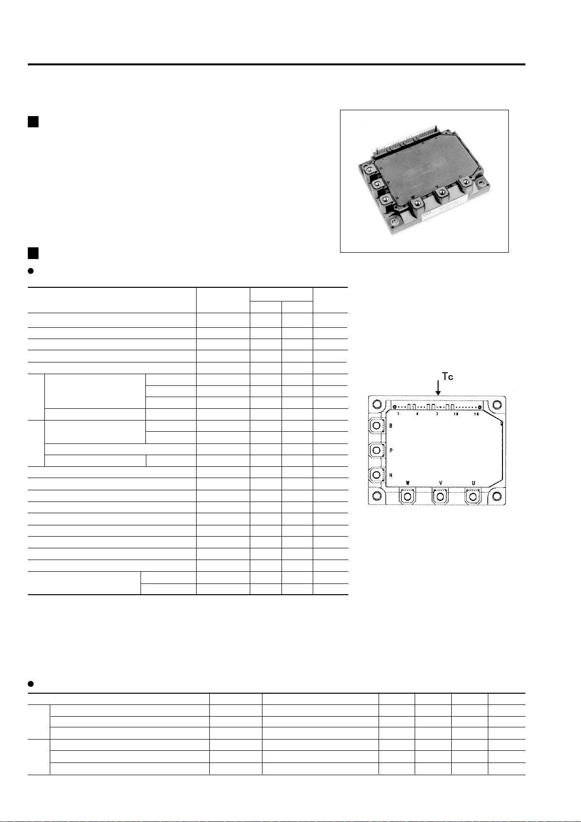
Fig.1 Measurement of case temperature
*1 Apply Vcc between terminal No. 3 and 1, 6 and 4, 9 and 7, 11 and 10.
*2 Apply Vin between terminal No. 2 and 1, 5 and 4, 8 and 7, 12,13,14,15 and 10.
*3 Apply VALM between terminal No. 16 and 10.
*4 Apply I
*5 50Hz/60Hz sine wave 1 minute.
ALM to terminal No. 16.
Electrical characteristics of power circuit (at Tc=Tj=25°C, Vcc=15V)
Item Symbol Condition Min. Typ. Max. Unit
INV Collector current at off signal input
Collector-Emitter saturation voltage
Forward voltage of FWD
DB Collector current at off signal input
Collector-Emitter saturation voltage
Forward voltage of Diode
ICES
VCE(sat)
VF
ICES
VCE(sat)
VF
VCE=600V input terminal open
Ic=150A
-Ic=150A
VCE=600V input terminal open
Ic=50A
-Ic=50A
– – 1.0 mA
– – 2.8 V
– – 3.0 V
– – 1.0 mA
– – 2.8 V
– – 3.3 V
Page 2

7MBP150RA060
IGBT-IPM
Electrical characteristics of control circuit(at Tc=Tj=25°C, Vcc=15V)
Item Symbol Condition Min. Typ. Max. Unit
Power supply current of P-line side Pre-driver(one unit)
Power supply current of N-line side three Pre-driver
Input signal threshold voltage (on/off)
Input zener voltage
Over heating protection temperature level
Hysteresis
IGBT chips over heating protection temperature level
Hysteresis
Collector current protection level INV
DB
Over current protection delay time
Under voltage protection level
Hysteresis
Alarm signal hold time
SC protection delay time
Limiting resistor for alarm
Iccp
ICCN
Vin(th)
VZ
TCOH
TCH
TjOH
TjH
IOC
IOC
tDOC
VUV
VH
tALM
tSC
RALM
fsw=0 to 15kHz Tc=-20 to 100°C *7
fsw=0 to 15kHz Tc=-20 to 100°C *7
ON
OFF
Rin=20k ohm
VDC=0V, Ic=0A, Case temperature Fig.1
surface of IGBT chips
Tj=125°C Collector current
Tj=125°C Collector current
Tj=25°C Fig.2
Tj=25°C Fig.3
3
10
1.00
1.25
110
150
225
75
-
11.0
0.2
1.5
1425
-
-
1.35
1.60
8.0
20
20
-
10
-
2
1500
18
65
1.70
1.95
125
-
-
-
-
-
-
12.5
-
12
1575
mA
mA
V
V
V
°C
°C
°C
°C
A
A
µs
V
V
ms
µs
ohm
*7 Switching frequency of IPM
Dynamic characteristics(at Tc=Tj=125°C, Vcc=15V)
Item Symbol Condition Min. Typ. Max. Unit
Switching time (IGBT)
Switching time (FWD)
Ioc
ton IC=150A, VDC=300V
toff
trr IF=150A, VDC=300V
0.3 - -
- - 3.6
- - 0.4
tsc
µs
µs
µs
Ic
ALM
I
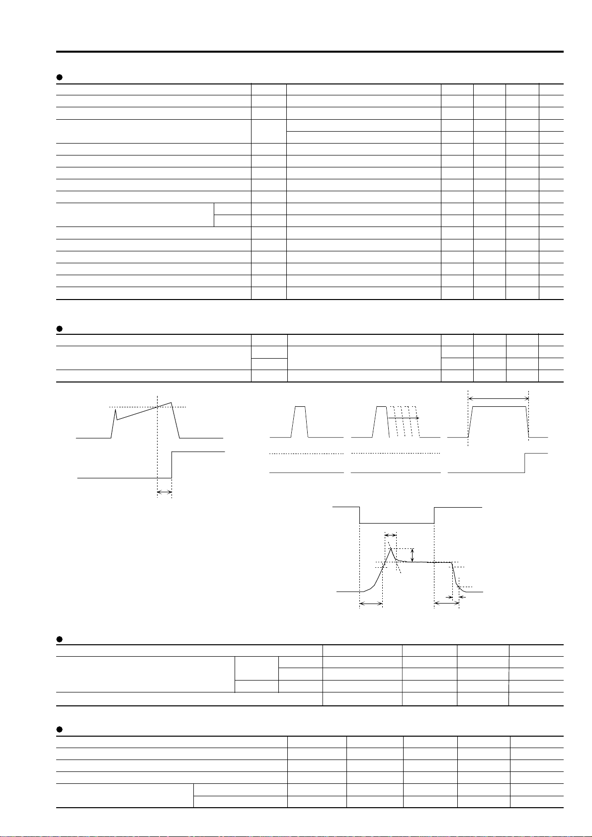
Fig.2Def i nit i onof OCDela yTime
ALM
I
DOC
t
Fig.3Definitionoftsc
Input Signal
CollectorCurrent
(Ic)
ALM
I
trr
Irr
90%
Fig.4Definition of Switching Time
IcIc Ic
ALM
I
90%
10%
tf
toffton
Thermal characteristics(Tc=25°C)
Item Symbol Typ. Max. Unit
Junction to Case thermal resistance
Case to fin thermal resistance with compound
INV IGBT
FWD
DB IGBT
Rth(j-c)
Rth(j-c)
Rth(j-c)
Rth(c-f)
- 0.21
- 0.47
- 0.63
0.05 -
°C/W
°C/W
°C/W
°C/W
Recommendable value
Item Symbol Min. Typ. Max. Unit
DC bus voltage
Operating power supply voltage range of Pre-driver
Switching frequency of IPM
Screw torque Mounting (M5)
Terminal (M5)
VDC 200 - 400 V
VCC 13.5 15 16.5 V
fSW 1 - 20 kHz
- 2.5 - 3.0 N·m
- 2.5 - 3.0 N·m
Page 3

7MBP150RA060
Block diagram
IGBT-IPM
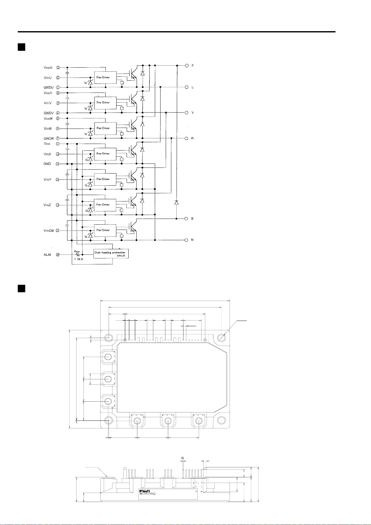
Pre-drivers include following functions
a) Short circuit protection circuit
b) Amplifier for driver
c) Undervoltage protection circuit
d) Over current protection circuit
e) IGBT chip over heating protection
Outline drawings, mm
±0.3
±0.3±0.3
±0.3
2
22
2
20
2020
2020
±1
±1±1
±1
±0.3
±0.3±0.3
±0.3
88
8888
88
74
7474
74
10
1010
10
2020
2017
1717
17
0.5
0.50.5
0.5
0.5
0.50.5
6‑M5
±1
±1
±1±1
109
109
109109
±0.3
±0.3
±0.3±0.3
95
95
10.16
10.16
10.1610.16
±0.15 ±0.15
±0.15±0.15
5.08
5.085.08
9595
67.4
67.4
67.467.4
±0.2 ±0.2
±0.2 ±0.25
±0.2±0.2
±0.2±0.2
10.16
10.1610.16
±0.15
±0.15±0.15
5.08
5.085.08
5.085.08
7
77
15.24
15.24
15.2415.24
2.54
2.54
2.542.54
1044447
1010
±0.3
±0.3
±0.3±0.3
13.8
13.8
13.813.8
3.22
3.22
3.223.22
±0.3
±0.3
±0.3±0.3
±0.2
±0.2 ±0.2
±0.2±0.2
10.16
10.16 10.16
10.1610.16
±0.15
±0.15 ±0.15
±0.15±0.15
5.08
5.08
5.085.08
111110
B
P
N
W
24
24 26
2424
V
26 26
2626
16‑
16‑ 2‑φ
16‑16‑
260.5
2626
0.64
0.64 2.5
0.640.64
±0.25
±0.25±0.25
±0.1
±0.1
±0.1±0.1
U
2‑φ
2‑φ2‑φ
4‑φ
4‑φ
5.5
5.5
4‑φ4‑φ
5.55.5
((((内内内内径径径径))))
16
16
1616
2.5
2.52.5
9
99
9
7
77
7
31
3131
‑0.3
+1.0
‑0.3‑0.3
‑0.3
+1.0+1.0
+1.0
22
2222
22
+1.0
‑0.2
+1.0+1.0
+1.0
‑0.2‑0.2
‑0.2
8
88
8
12.5
12.512.5
12.5
31
‑0.3
+1.0
‑0.3‑0.3
‑0.3
+1.0+1.0
+1.0
22
2222
22
17
1717
17
Mass : 440g
Page 4

7MBP150RA060
Characteristics (Representative)
Control Circuit
IGBT-IPM
Page 5

7MBP150RA060
Inverter
IGBT-IPM
Page 6

7MBP150RA060
IGBT-IPM
Page 7

7MBP150RA060
IGBT-IPM
Page 8

7MBP150RA060
Brake
IGBT-IPM
 Loading...