

Page 1
7MBP100RA120
IGBT-IPM R series
Features
· Temperature protection provided by directly detecting the junction
temperature of the IGBTs
· Low power loss and soft switching
· High performance and high reliability IGBT with overheating protection
· Higher reliability because of a big decrease in number of parts in
built-in control circuit
Maximum ratings and characteristics
Absolute maximum ratings(at Tc=25°C unless otherwise specified)
Item
DC bus voltage
DC bus voltage (surge)
DC bus voltage (short operating)
Collector-Emitter voltage
DB Reverse voltage
INV Collector current DC
1ms
DC
Collector power dissipation One transistor
DB Collector current DC
1ms
Forward current of Diode
Collector power dissipation One transistor
Junction temperature
Input voltage of power supply for Pre-Driver
Input signal voltage
Input signal current
Alarm signal voltage
Alarm signal current
Storage temperature
Operating case temperature
Isolating voltage (Case-Terminal)
Screw torque Mounting (M5)
Terminal (M5)
Symbol Rating Unit
Min. Max.
VDC
VDC(surge)
VSC
VCES
VR
IC
ICP
-IC
PC
IC
ICP
IF
PC
Tj
VCC *1
Vin *2
Iin
VALM *3
IALM *4
Tstg
Top
Viso *5
0
0
200
0
-
-
-
-
-
-
-
-
-
0
0
0
-
-40
-20
-
-
-
900
1000
800
1200
1200
100
200
100
735
50
100
50
400
150
20
Vz
1
Vcc
15
125
100
AC2.5
3.5 *6
3.5 *6
1200V / 100A 7 in one-package
V
V
V
V
V
A
A
A
W
A
A
A
W
°C
V
V
mA
V
mA
°C
°C
kV
N·m
N·m
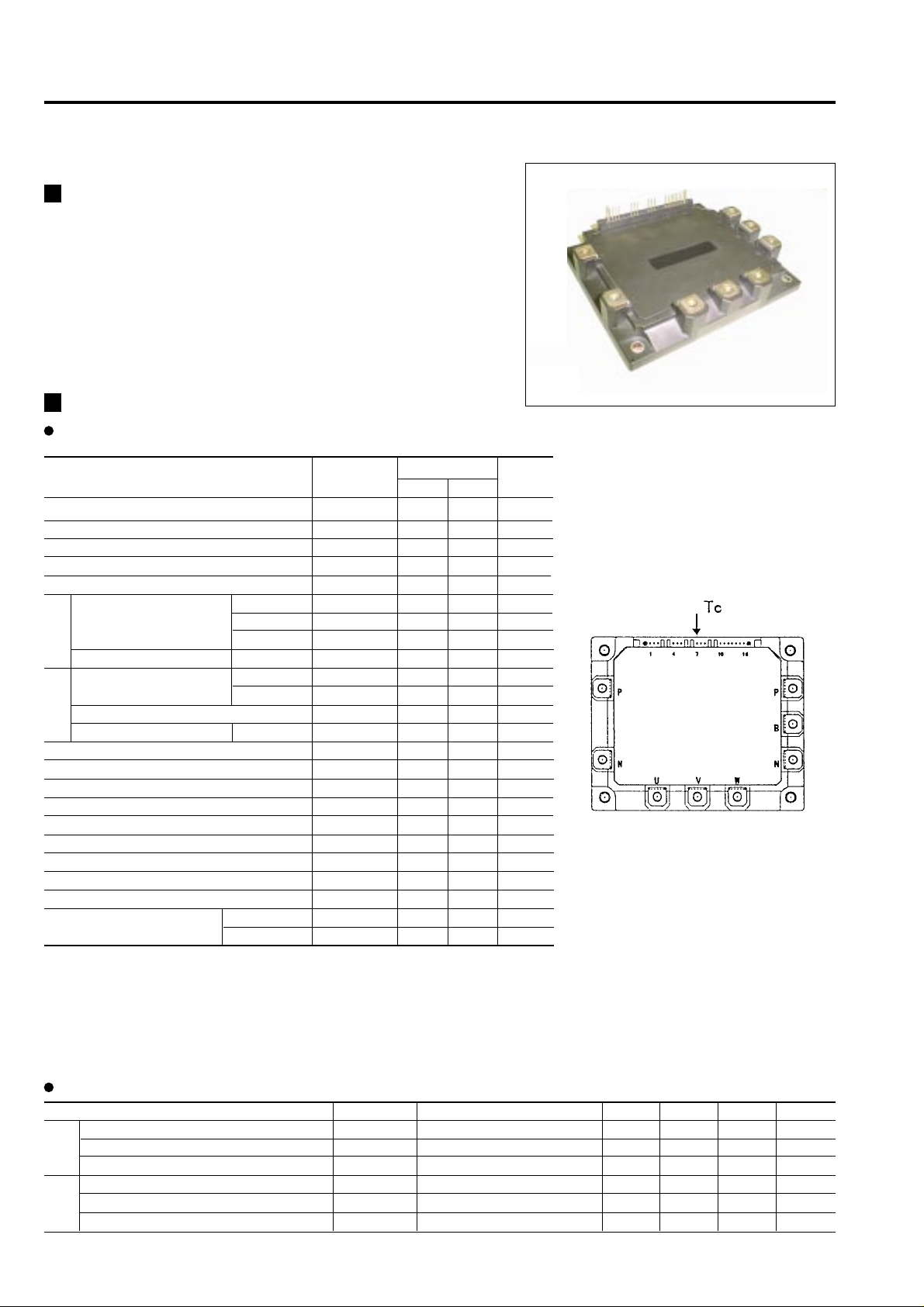
Fig.1 Measurement of case temperature
*1 Apply Vcc between terminal No. 3 and 1, 6 and 4, 9 and 7, 11 and 10.
*2 Apply Vin between terminal No. 2 and 1, 5 and 4, 8 and 7, 12,13,14,15 and 10.
*3 Apply VALM between terminal No. 16 and 10.
*4 Apply I
*5 50Hz/60Hz sine wave 1 minute.
*6 Recommendable Value : 2.5 to 3.0 N·m
ALM to terminal No. 16.
Electrical characteristics of power circuit (at Tc=Tj=25°C, Vcc=15V)
Item Symbol Condition Min. Typ. Max. Unit
INV Collector current at off signal input
Collector-Emitter saturation voltage
Forward voltage of FWD
DB Collector current at off signal input
Collector-Emitter saturation voltage
Forward voltage of Diode
ICES
VCE(sat)
VF
ICES
VCE(sat)
VF
VCE=1200V input terminal open
Ic=100A
-Ic=100A
VCE=1200V input terminal open
Ic=50A
-Ic=50A
– – 1.0 mA
– – 2.6 V
– – 3.0 V
– – 1.0 mA
– – 2.6 V
– – 3.3 V
Page 2
7MBP100RA120
IGBT-IPM
Electrical characteristics of control circuit(at Tc=Tj=25°C, Vcc=15V)
Item Symbol Condition Min. Typ. Max. Unit
Power supply current of P-line side Pre-driver(one unit)
Power supply current of N-line side three Pre-driver
Input signal threshold voltage (on/off)
Input zener voltage
Over heating protection temperature level
Hysteresis
IGBT chips over heating protection temperature level
Hysteresis
Collector current protection level INV
DB
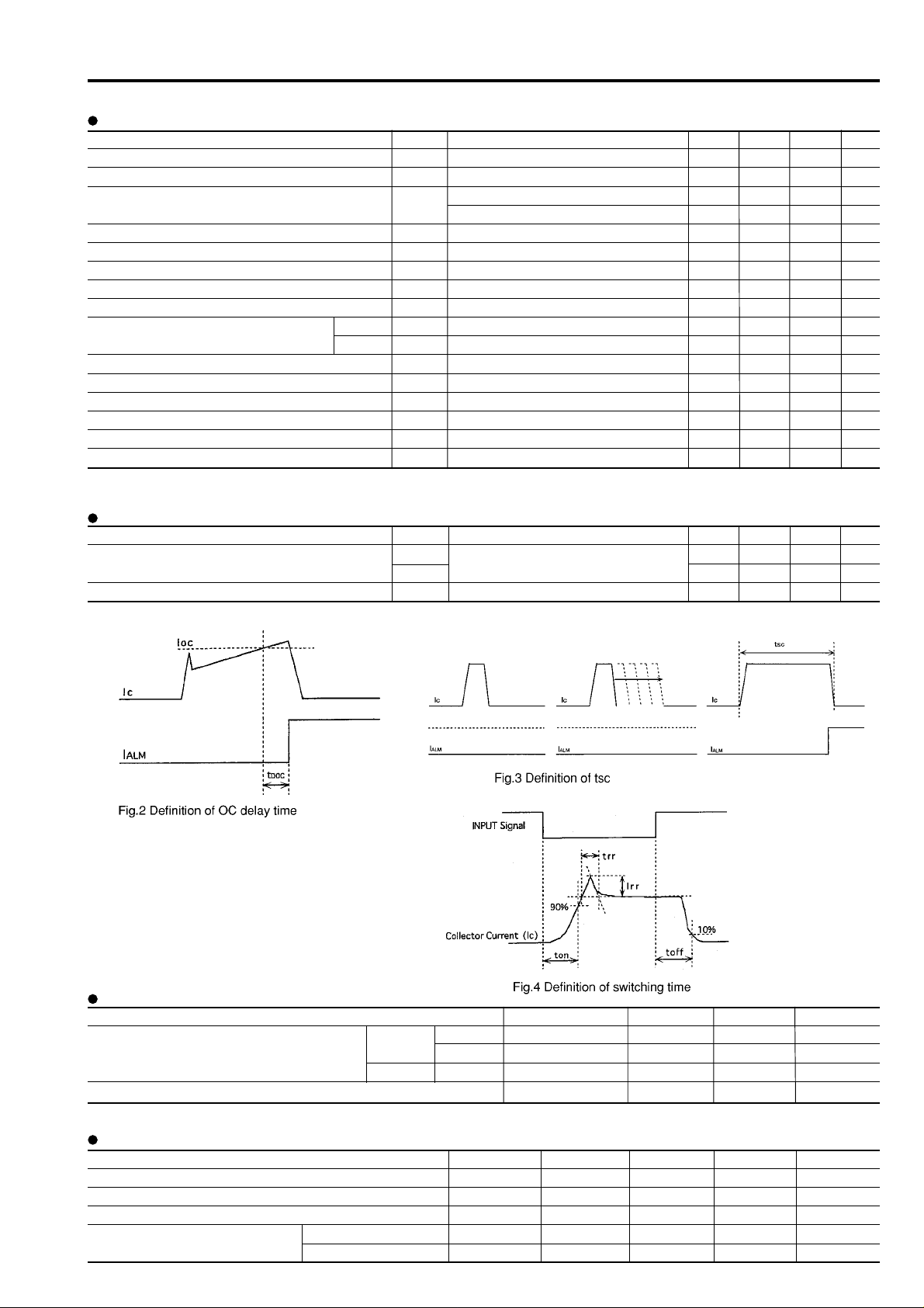
Over current protection delay time
Under voltage protection level
Hysteresis
Alarm signal hold time
SC protection delay time
Limiting resistor for alarm
*7 Switching frequency of IPM
Iccp
ICCN
Vin(th)
VZ
TCOH
TCH
TjOH
TjH
IOC
IOC
tDOC
VUV
VH
tALM
tSC
RALM
fsw=0 to 15kHz Tc=-20 to 100°C *7
fsw=0 to 15kHz Tc=-20 to 100°C *7
ON
OFF
Rin=20k ohm
VDC=0V, Ic=0A, Case temperature Fig.1
surface of IGBT chips
Tj=125°C
Tj=125°C
Tj=25°C Fig.2
Tj=25°C Fig.3
3
10
1.00
1.70
110
150
150
75
-
11.0
0.2
1.5
1425
-
-
1.35
2.05
8.0
20
20
-
10
-
2
1500
18
65
1.70
2.40
125
-
-
-
-
-
-
12.5
-
12
1575
mA
mA
V
V
V
°C
°C
°C
°C
A
A
µs
V
V
ms
µs
ohm
Dynamic characteristics(at Tc=Tj=125°C, Vcc=15V)
Item Symbol Condition Min. Typ. Max. Unit
Switching time (IGBT)
Switching time (FWD)
ton IC=100A, VDC=600V
toff
trr IF=100A, VDC=600V
0.3 - -
- - 3.6
- - 0.4
µs
µs
µs
Thermal characteristics(Tc=25°C)
Item Symbol Typ. Max. Unit
Junction to Case thermal resistance
Case to fin thermal resistance with compound
INV IGBT
FWD
DB IGBT
Rth(j-c)
Rth(j-c)
Rth(j-c)
Rth(c-f)
- 0.17
- 0.36
- 0.31
0.05 -
°C/W
°C/W
°C/W
°C/W
Recommendable value
Item Symbol Min. Typ. Max. Unit
DC bus voltage
Operating power supply voltage range of Pre-driver
Switching frequency of IPM
Screw torque Mounting (M5)
Terminal (M5)
VDC 200 - 800 V
VCC 13.5 15 16.5 V
fSW 1 - 20 kHz
- 2.5 - 3.0 N·m
- 2.5 - 3.0 N·m
Page 3
7MBP100RA120
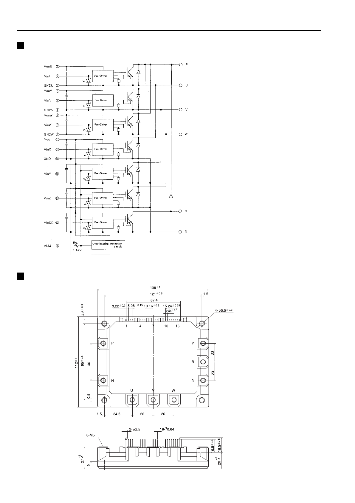
Block diagram
IGBT-IPM
Pre-drivers include following functions
a) Amplifier for driver
b) Short circuit protection
c) Undervoltage lockout circuit
d) Over current protection
e) IGBT chip over heating protection
Outline drawings, mm
Mass : 920g
Page 4

7MBP100RA120
Characteristics (Representative)
control circuit
Power supply current v s. Switching frequency
70
P-side
60
50
40
N-side
Tj=100°C
Vcc=17V
Vcc=15V
Vcc=13V
Input signal threshold volta ge
vs. Power supply vo ltage
2.5
2
1.5
IGBT-IPM
Tj=25°C
Tj=125°C
} Vin(off)
} Vin(on)
30
20
Power supply current : Icc (mA)
10
0
0 5 10 15 20 25
Switching frequency : fsw (kHz)
Under voltage vs. Junction temperature
14
12
10
8
6
4
Under vo lt a g e : VUVT (V )
2
Vcc=17V
Vcc=15V
Vcc=13V
1
: Vin(on),Vin(off) (V)
Input signal threshold voltage
0.5
0
12 13 14 15 16 17 18
Power supply voltage : Vcc (V)
Under voltage hysterisis vs. Jnction temperature
1
0.8
0.6
0.4
0.2
Under voltage hysterisis : VH (V)
0
20 40 60 80 100 120 140
Junction temperature : Tj (°C)
Alarm hold time vs. Power supply voltage
3
2.5
Tj=125°C
2
1.5
1
0.5
Alarm hold time : tALM (mSec)
0
12 13 14 15 16 17 18
Power supply voltage : Vcc (V)
Tj=25°C
0
20 40 60 80 100 120 140
Junction temperature : Tj (°C)
Over heating characteristics
TcOH,TjOH,TcH,TjH vs. Vcc
200
TjOH
150
TcOH
100
50
OH hy st er i si s : Tc H, Tj H (°C )
Over heating pr otection : TcOH,T jOH ( °C)
0
12 13 14 15 16 17 18
Power supply voltage : Vcc (V)
TcH,TjH
Page 5

7MBP100RA120
j
Inverter
IGBT-IPM
Collector current vs. Collector-Emitter voltage
T
160
140
120
100
80
60
Collector Current : Ic (A)
40
20
0
0 0.5 1 1.5 2 2.5 3
Collector-Emitter voltage : Vce (V)
=25°C
Vcc=17V
Switching time vs. Collector current
10000
1000
Edc=600V,Vcc=15V,Tj=25°C
Vcc=15V
Vcc=13V
toff
ton
Collector current vs. Collector-Emitter voltage
Tj=125°C
160
140
120
100
80
60
40
Collector Current : Ic (A)
20
0
00.511.522.53
Collector-Emitter voltage : Vce (V)
Vcc=17V
Switching time vs. Collector current
10000
1000
Edc=600V,Vcc=15V,Tj=125°C
toff
Vcc=15V
Vcc=13V
ton
100
Switching time : ton,toff,tf (nSec)
10
0 20406080100120140160
Collector current : Ic (A)
Forward current vs. Forward voltage
160
140
120
100
80
60
40
Forward Current : If (A)
20
125°C
tf
tf
100
Switching time : ton,toff,tf (nSec)
10
020406080100120140160
Collector current : Ic (A)
Reverse recovery characteristics
trr,Irr vs. IF
trr125°C
25°C
100
trr25°C
Irr125°C
Irr25°C
Reverse recovery current : Irr(A)
Reverse recovery time : trr(nSec)
0
00.511.522.53
Forward voltage : Vf (V)
10
0 20406080100120140160
Forward curr ent : IF(A)
Page 6

7MBP100RA120
IGBT-IPM
Transient ther m a l resistance
1
0.1
Thermal resist ance : Rth(j-c) (°C/ W)
0.01
0.001 0.01 0.1 1
Pulse width :Pw (sec)
Power derating for IGBT
(per device)
800
700
FWD
IGBT
Reversed biased safe operating area
1400
Vcc=15V,Tj 125°C
1200
1000
800
SCSOA
600
400
Collector current : Ic (A)
200
0
0 200 400 600 800 1000 1200 1400
(non-repetitive pulse)
RBSOA
(Repetitive pulse)
Collector-Emitter voltage : Vce (V)
<
=
Powe r der ating for FWD
(per device)
350
300
600
500
400
300
200
100
Collecter Power Diss i pation : Pc (W)
0
0 20406080100120140160
Case Temperature : Tc (°C)
Switching Loss vs. Collector Current
Edc=600V,Vcc=15V,Tj=25°C
40
35
30
25
20
Eon
250
200
150
100
50
Collecter Power Diss ipation : Pc (W)
0
0 20406080100120140160
Case Temperature : Tc (°C)
Switching Loss vs. Collector Current
Edc=600V,Vcc=15V,Tj=125°C
40
35
30
25
20
Eon
Eoff
15
10
5
Switching loss : Eon,Eoff,Err (mJ/cycle)
0
0 20406080100120140160
Collector current : Ic (A)
Eoff
Err
15
10
5
Switching loss : Eon,Eoff,Err (mJ/cycle)
0
0 20406080100120140160
Collector current : Ic (A)
Err
Page 7

7MBP100RA120
Over current protection vs. Junction temperature
400
350
300
250
200
150
100
Over current protection level : Ioc(A)
50
0
020406080100120140
Junction temperature : Tj(°C)
IGBT-IPM
Vcc=15V
Page 8

7MBP100RA120
j
)
j
)
Brake
IGBT-IPM
Collector current vs. Collector-Emitter voltage
=25°C
80
T
70
60
50
40
30
Collector Current : Ic (A)
20
10
0
0 0.5 1 1.5 2 2.5 3
Collector-Emitter voltage : Vce (V
Vcc=15V
Vcc=17V
Vcc=13V
Transient ther m a l resistance
1
IGBT
Collector current vs. Collector-Emitter voltage
=125°C
80
70
60
50
40
30
Collector Current : Ic (A)
20
10
0
0 0.5 1 1.5 2 2.5 3
T
Vcc=17V
Coll e ctor-Emitter voltage : Vce (V
Reversed biased safe operating area
700
600
500
Vcc=15V,Tj 125°C
Vcc=15V
Vcc=13V
0.1
Thermal resist ance : Rth(j-c) (°C/ W)
0.01
0.001 0.01 0.1 1
Pulse width :Pw (sec)
Power derating for IGBT
(per device)
400
350
300
250
200
150
400
SCSOA
300
200
Collector current : Ic (A)
100
0
0 200 400 600 800 1000 1200 1400
(non-re pet iti v e p ulse)
RBSOA
(Repetitive pulse)
Collector-Emitter voltage : Vce (V)
Over current protection vs. Junction temperature
Vcc=15V
200
150
100
100
Collecter Power Dissipation : Pc (W)
50
0
0 20 40 60 80 100 120 140 160
Case Tempe r ature : Tc (°C)
50
Over current protection level : Ioc(A)
0
0 20 40 60 80 100 120 140
Junction temperature : Tj(°C)
 Loading...