

Fuji Electric 6MBP20XSD060-50, 6MBP15XSD060-50, 6MBP15XSF060-50, 6MBP20XSF060-50, 6MBP30XSD060-50 Applications Manual
...Page 1
Fuji IGBT Intelligent-Power-Module
“Small-IPM"
Application Manual
6MBP15XS*060-50
6MBP20XS*060-50
6MBP30XS*060-50
6MBP35XS*060-50
Fuji Electric Co., Ltd.
MT6M12343 Rev.1.0
Dec.-2016
Fuji Electric Co., Ltd.
Dec. 2016
Page 2

CONTENTS
Chapter 1 Product Outline
1. Introduction .......................................................................................... 1-2
2. Product line-up ..................................................................................... 1-4
3. Definition of Type Name and Marking Spec.......................................... 1-5
4. Package outline dimensions.................................................................. 1-6
5. Absolute Maximum Ratings ................................................................. 1-7
Chapter 2 Description of Terminal Symbols and Terminology
1. Description of Terminal Symbols ........................................................ 2-2
2. Description of Terminology ................................................................. 2-3
Chapter 3 Detail of Signal Input/Output Terminals
1. Control Power Supply Terminals V
2. Power Supply Terminals of High Side VB(U,V,W) .............................. 3-6
3. Function of Internal BSDs (Boot Strap Diodes) ................................... 3-9
4. Input Terminals IN(HU,HV,HW), IN(LU,LV,LW) .................................. 3-13
5. Over Current Protection Input IS ......................................................... 3-16
6. Fault Status Output VFO ..................................................................... 3-17
7. Linear Temperature Sensor Output TEMP .......................................... 3-18
8. Over Heat Protection ........................................................................... 3-20
Chapter 4 Power Terminals
1. Connection of Bus Input terminal and Low Side Emitters .................... 4-2
2. Setting of Shunt Resistor of Over Current Protection .......................... 4-3
Chapter 5 Recommended wiring and layout
1. Examples of Application Circuits.......................................................... 5-2
2. Recommendation and Precautions in PCB design ............................. 5-5
Chapter 6 Mounting Guideline and Thermal Design
1. Soldering to PCB ................................................................................. 6-2
2. Mounting to Heat sink .......................................................................... 6-3
3. Cooler (Heat Sink) Selection................................................................ 6-4
Chapter 7 Cautions
1. Other warnings and precautions ......................................................... 7-2
2. Handling and storage precautions ...................................................... 7-2
3. Notice .................................................................................................. 7-3
CCH,VCCL
,COM .............................. 3-2
Fuji Electric Co., Ltd.
MT6M12343 Rev.1.0
Dec.-2016
Page 3

Chapter 1
Product Outline
Contents Page
1. Introduction .................... .......................................................................... 1-2
2. Product line-up ......................................................................................... 1-4
3. Definition of type name and marking spec .............................................. 1-5
4. Package outline dimensions .................................................................... 1-6
5. Absolute maximum ratings ...................................................................... 1-7
Fuji Electric Co., Ltd.
MT6M12343 Rev.1.0
Dec.-2016
1-1
Page 4
Chapter 1 Product Outline
VB(U)
11
10
9
5
3
21
20
19
18
17
16
15
14
13
12
22
23
24
26
28
30
36
32UP
V
W
N(V)
N(U)
N(W)
Vcc
IN
GND
OUT
Vs
Vcc
U
IN
V
IN
W
IN
U
OUT
V
OUT
W
OUT
Fo
IS
GND
VFO
IS
COM
COM
IN(LU)
IN(LV)
IN(LW)
V
CCL
V
CCH
IN(HU)
IN(HV)
IN(HW)
VB(V)
VB(W)
TEMP
NC
V
B
7
TEMP
Vcc
IN
GND
OUT
Vs
V
B
Vcc
IN
GND
OUT
Vs
V
B
3×HVIC
LVIC
3×BSD
6×IGBT 6×FWD
1. Introduction
The objective of this document is introducing Fuji IGBT Intelligent-Power-Module “Small-IPM”.
At first, the product outline of this module is described.
Secondary, the terminal symbol and terminology used in this note and the specification sheet are
explained. Next, the design guideline on signal input terminals and power terminals are shown using its
structure and behavior. Furthermore, recommended wiring and layout, and the mount guideline are given.
Feature and functions
1.1 Product concept
• 7th gen. IGBT technology offers high-efficiency and energy-saving operation.
• Guarantee T
• Higher accuracy of short circuit detection contribute to expanding over load operating area.
• Compatible pin assignment, foot print size and mounting dimensions as the 1st gen. Small IPM series.
• Product range: 15A – 35A / 600V.
• The total dissipation loss has been improved by improvement of the trade-off between the Collector-
Emitter saturation voltage V
1.2 Built-in drive circuit
• Drives the IGBT under optimal conditions.
• The control IC of upper side arms have a built-in high voltage level shift circuit (HVIC).
• This IPM is possible for driven directly by a microprocessor. Of course, the upper side arm can also
be driven directly. The voltage level of input signal is 3.3V or 5V.
• Since the wiring length between the internal drive circuit and IGBT is short and the impedance of the
drive circuit is low, no reverse bias DC source is required.
• This IPM device requires four control power sources. One is a power supply for the lower side IGBTs
and control ICs. The other three power supplies are power supplies for the upper side IGBTs with
proper circuit isolation.
The IPM doesn’t need insulated power supplies for the upper side drive because the IPM has built-in
bootstrap diodes (BSD).
j(ope)
=150℃
and switching loss.
CE(sat)
Fuji Electric Co., Ltd.
MT6M12343 Rev.1.0
Dec.-2016
Fig. 1-1 Block Diagram of Internal Circuit
1-2
Page 5
Chapter 1 Product Outline
FWDIGBT
WIREIC
Mold resin
Lead frame
BSD
Aluminum base PCB with isolation layer
Mold resin
FWDIGBT
WIREIC
Mold resin
Lead frame
BSD
Aluminum base PCB with isolation layer
Mold resin
1.3 Built-in protection circuits
• The following built-in protection circuits are incorporated in the IPM device:
(OC): Over current protection
(UV): Under voltage protection for power supplies of control IC
(LT) or (OH): Temperature sensor output function or Overheating protection
(FO): Fault alarm signal output
• The OC protection circuits protect the IGBT against over current, load short-circuit or arm short-circuit.
The protection circuit monitors the emitter current using external shunt resistor in each lower side IGBT
and thus it can protect the IGBT against arm short-circuit.
• The UV protection circuit is integrated into all of the IGBT drive circuits and control power supply. This
protection function is effective for a voltage drop of all of the high side drive circuits and the control
power supply.
• The OH protection circuit protects the IPM from overheating. The OH protection circuit is built into the
control IC of the lower side arm (LVIC).
• The temperature sensor output function enables to output measured temperature as an analog voltage
(built in LVIC)
• The FO function outputs a fault signal, making it possible to shut down the system reliably by outputting
the fault signal to a microprocessor unit which controls the IPM when the circuit detects abnormal
conditions.
1.4 Compact package
•The package of this product includes with an aluminum base, which further improves the heat radiation.
•The control input terminals have a shrink pitch of 1.778mm (70mil).
•The power terminals have a standard pitch of 2.54mm (100mil).
Fig.1-2 Package overview
Fuji Electric Co., Ltd.
MT6M12343 Rev.1.0
Dec.-2016
Fig.1-3 Package cross section diagram
1-3
Page 6

Chapter 1 Product Outline
2. Product line-up and applicable products for this manual
Table. 1-1 Line-up
Rating of IGBT
Type name
6MBP15XSD060-50 600
6MBP15XSF060-50 LT*1
Voltage
[V]
Current
[A]
15 1500Vrms
Sinusoidal 60Hz, 1min.
(Between shorted all terminals and case)
Isolation Voltage
[Vrms]
Variation Target application
*1
LT
OH
6MBP20XSD060-50 20 LT
*1
6MBP20XSF060-50 LT*1
OH
6MBP30XSD060-50 30 LT*1
6MBP30XSF060-50 LT
*1
OH*1
6MBP35XSD060-50 35 LT*1
6MBP35XSF060-50 LT
*1
OH*1
*1
*1
・Room air conditioner
compressor drive
・Heat pump
applications
・Fan motor drive
・General motor drive
・Servo drive
*1 (LT): Temperature sensor output function (LT)
(OH): Overheating protection function (OH)
Fuji Electric Co., Ltd.
MT6M12343 Rev.1.0
Dec.-2016
1-4
Page 7
Chapter 1 Product Outline
A1 A2
6MBP15XSD060-50 L D
6MBP15XSF060-50 L F
6MBP20XSD060-50 M D
6MBP20XSF060-50 M F
6MBP30XSD060-50 O D
6MBP30XSF060-50 O F
6MBP35XSD060-50 P D
6MBP35XSF060-50 P F
TYPE NAME
PRODUCT CODE
3. Definition of Type Name and Marking Spec.
• Type name
6 MBP 20 X S D 060 –50
Additional model number (Option)
50 : RoHS
Voltage rating
060 : 600V
Additional number of series
D : Temperature sensor output
F : Temperature sensor output and Over heating protection
Series name
S: Package type
Series name
X: Chip generation
IGBT current rating
15: 15A, 20: 20A, 30: 30A, 35: 35A
Indicates IGBT-IPM
Number of switch elements
6 : 6-chip circuit of three phase bridge
A
Trademark
1
Type Name
Y
6MBP20XSD
060-50
M
DATE CODE & Serial number
YMNNNN
Y : Year (0 to 9)
M : Month (1 to 9 and O, N, D)
NNNN : Serial number
Products code
A
2
Country of Origin mark
“” (Bank) : Japan
P : Philippine
P
270001
Year Code (0 to 9)
Month Code (1 to 9 and O, N, D)
Fuji Electric Co., Ltd.
MT6M12343 Rev.1.0
Dec.-2016
Fig.1-4 Marking Specification
1-5
Page 8
Chapter 1 Product Outline
A
DETAIL A
14.13
14x2.54 (=35.56)
13.0
3.50(min.)
43.0
35.0
26.0
18x1.778(=32.004)
±0.5
±0.3
±0.5
4.2
1.6 ±0.1
±0.1
3.2
±0.1
14.0
14.7
29.4
±0.5
±0.5
±0.5
1.8
1.5
3.7
±0.1
±0.1
0
.
40
10.6
±0.1
1.8
±0.1
2.5(min)
(1.2 )
(0.6)
8.96
15.56
3579101112131415161718192021
22 23 24 26 28 30 32 36
±0.1
0.98(min.)
Note.1
The IMS (Insulated Metal Substrate) deliberately protruded from back surface of case.
It is improved of thermal conductivity between IMS and heat-sink.
4.76 ±0.3
15.56
±0.3
※ Note.1
Solder Plating
5.63
±0.25
0.7 ±0.4
±0.3
8.58(min.)
3.50(min.)
13.0
30.4
±0.3
±0.3
±0.3
Insulated Metal
Substrate
2.54
±0.2
1.778±0.2
B
±0
.
1
0
.
40
±
0
.
1
D
Insulated Metal
Substrate
DETAIL B
DETAIL C
DETAIL D
C
0.6
0.9
0.6
1.2
2.5(min)
3.50(min.)
±0.1
±0.1
±0.1
±0.1
±0.5
±0.5
3.83
2.6
±0.1
0.13±0.13
Unit: mm
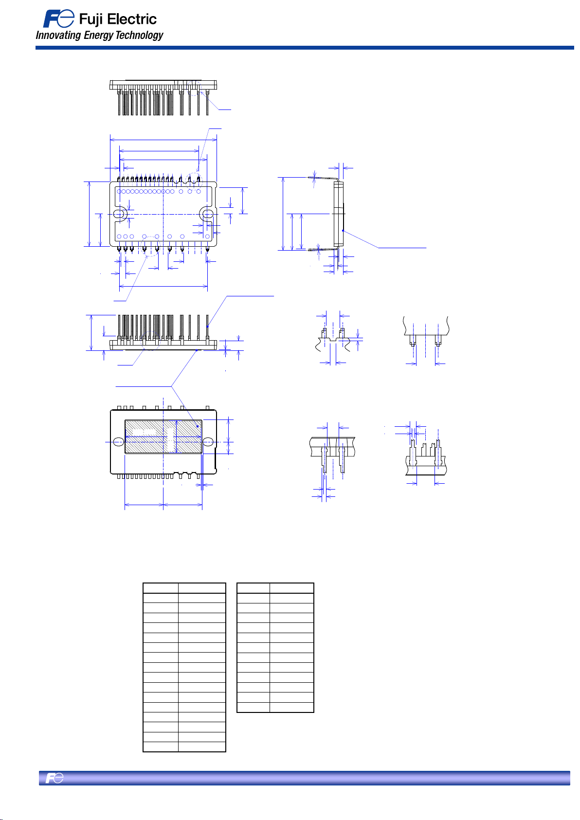
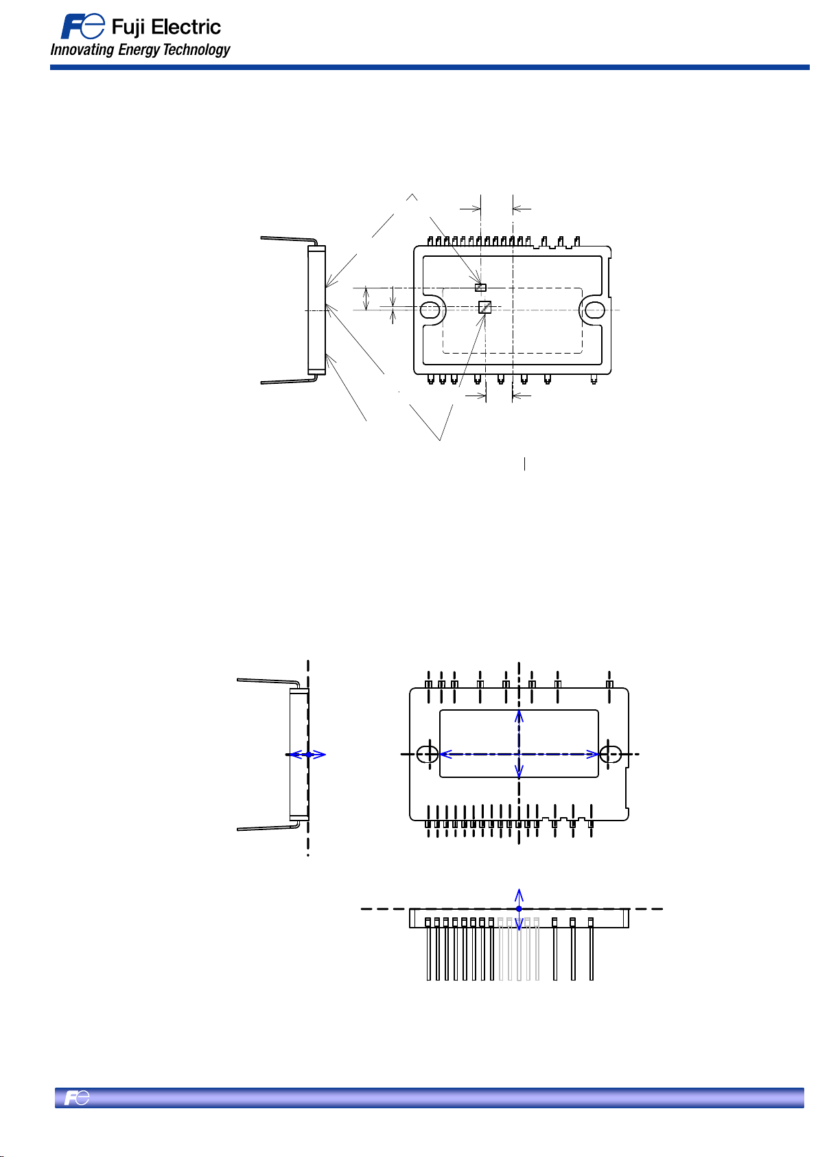
4. Package outline dimensions
Pin No. Pin Name
3 VB(U)
5 VB(V)
7 VB(W)
9 IN(HU)
10 IN(HV)
11 IN(HW)
12 V
13 COM
14 IN(LU)
15 IN(LV)
16 IN(LW)
17 V
18 VFO
19 IS
20 COM
21 Temp
CCH
CCL
Pin No. Pin Name
22 N(W)
23 N(V)
24 N(U)
26 W
28 V
30 U
32 P
36 NC
Fig.1-5. Case outline drawings
Fuji Electric Co., Ltd.
MT6M12343 Rev.1.0
Dec.-2016
1-6
Page 9

Chapter 1 Product Outline
5. Absolute Maximum Ratings
An example of the absolute maximum ratings of 6MBP20XSD060-50 is shown in Table 1-2.
Table 1-2 Absolute Maximum Ratings at Tj=25C,Vcc=15V (unless otherwise specified)
Item Symbol Rating Unit Description
DC bus Voltage V
Bus Voltage (Surge) V
Collector-Emitter Voltage V
Collector Current I
Peak Collector Current I
Diode Forward Current I
Peak Diode Forward Current I
Collector Power Dissipation P
FWD Power Dissipation P
DC
DC(Surge)
CES
C@25
CP@25
F@25
FP@25
D_IGBT
D_FWD
450 V
500 V
600 V
20
40
A
A
20 A
40 A
41.0 W
27.8 W
DC voltage that can be applied between
P-N(U),N(V),N(W) terminals
Peak value of the surge voltage that can be
applied between P-N(U),N(V),N(W)
terminals during switching operation
Maximum collector-emitter voltage of the
built-in IGBT chip and repeated peak
reverse voltage of the FWD chip
Maximum collector current for the IGBT chip
Tc=25C, Tj=150C
Maximum pulse collector current for the
IGBT chip Tc=25C, Tj=150C
Maximum forward current for the FWD chip
Tc=25C, Tj=150C
Maximum pulse forward current for the
FWD chip Tc=25C, Tj=150C
Maximum power dissipation for one IGBT
element at Tc=25C, Tj=150C
Maximum power dissipation for one FWD
element at Tc=25C, Tj=150C
Maximum Junction Temperature
of Inverter Block
Operating Junction Temperature
of Inverter Block
T
T
j(max)
jOP
+150
-40 ~ +150
Maximum junction temperature of the IGBT
C
chips and the FWD chips
Junction temperature of the IGBT and FWD
C
chips during continuous operation
Fuji Electric Co., Ltd.
MT6M12343 Rev.1.0
Dec.-2016
1-7
Page 10

Chapter 1 Product Outline
Table 1-2 Absolute Maximum Ratings at Tj=25C,Vcc=15V (Continued)
Item Symbol Rating Unit Descriptions
High-side Supply Voltage V
Low-side Supply Voltage V
High-side Bias Supply Voltage
High-side Bias Voltage for IGBT
Gate Driving
Input Signal Voltage V
Input Signal Current I
Fault Signal Voltage V
Fault Signal Current I
Over Current Sensing
Input Voltage
CCH
CCL
V
B(U)-COM
V
B(V)-COM
V
B(W)-COM
V
B(U)
V
B(V)
V
B(W)
IN
IN
FO
FO
V
IS
-0.5 ~ 20 V
-0.5 ~ 20 V
Voltage that can be applied between COM
and V
terminal
CCH
Voltage that can be applied between COM
and V
terminal
CCL
Voltage that can be applied between VB(U)
-0.5 ~ 620 V
terminal and COM, VB(V) terminal and
COM,VB(W) terminal and COM.
20 V
Voltage that can be applied between U
terminal and VB(U) terminal , V terminal and
VB(V) terminal , W terminal and VB(W)
terminal.
-0.5 ~ V
-0.5 ~ V
-0.5 ~ V
-0.5 ~ V
+0.5
CCH
CCL
+0.5
V
3 mA
+0.5 V
CCL
1 mA
+0.5 V
CCL
Voltage that can be applied between COM
and each IN terminal
Maximum input current that flows from IN
terminal to COM
Voltage that can be applied between COM
and VFO terminal
Sink current that flows from VFO to COM
terminal
Voltage that can be applied between IS and
COM terminal
Maximum Junction Temperature
of Control Circuit Block
Operating Case Temperature T
Storage Temperature T
Isolation Voltage V
T
j
+150
Maximum junction temperature of the
C
control circuit block
Operating case temperature (temperature of
c
-40 ~ +125
C
the aluminum plate directly under the IGBT
or the FWD)
Range of ambient temperature for storage
stg
-40 ~ +125
C
or transportation, when there is no electrical
load
Maximum effective value of the sine-wave
iso
AC 1500 Vrms
voltage between the terminals and the heat
sink, when all terminals are shorted
simultaneously. (Sine wave = 60Hz / 1min)
Fuji Electric Co., Ltd.
MT6M12343 Rev.1.0
Dec.-2016
1-8
Page 11
Chapter 1 Product Outline
The Collector Emitter Voltages specified in absolute maximum rating
The absolute maximum rating of collector-emitter voltage of the IGBT is specified below.
During operation of the IPM, the voltage between P and N(*) is usually applied to one phase of upper or
lower side IGBT. Therefore, the voltage applied between P and N(*) must not exceed absolute maximum
ratings of IGBT. The Collector-Emitter voltages specified in absolute maximum rating are described below.
N(*): N(U),N(V),N(W)
V
CES
V
DC
V
DC(Surge)
:Absolute Maximum rating of IGBT Collector Emitter Voltage.
:DC bus voltage Applied between P and N(*).
:The total of DC bus voltage and surge voltage which generated by the wiring
(or pattern) inductance from P-N(*) terminal to the bulk capacitor.
≤ VDC(Surge)
Collector-Emitter Current
≤ VDC(Surge)
≤ VDC
≤ VDC
VCE,IC=0
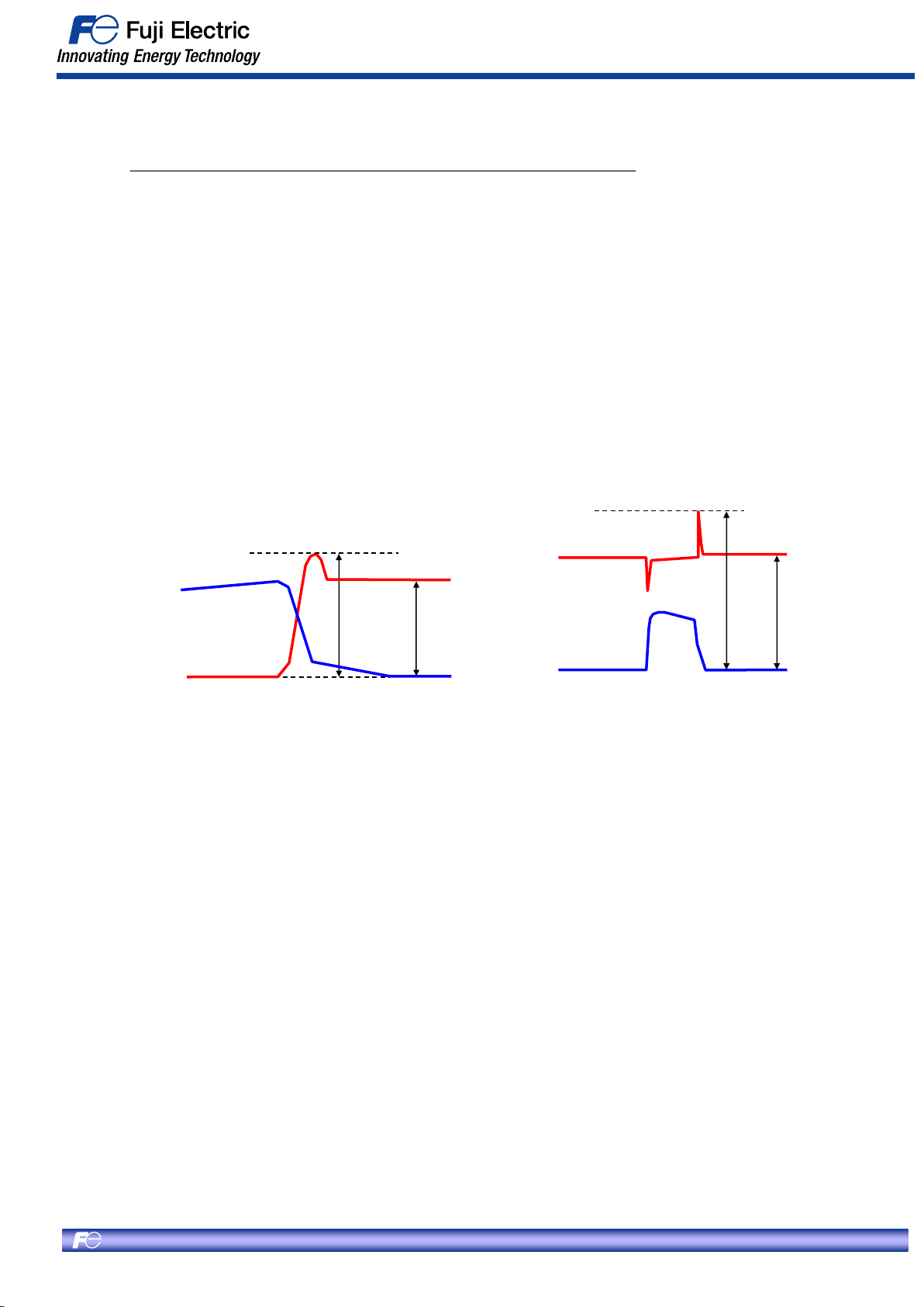
(a) In Turn-off Switching (b) In Short-circuit
Short-circuit Current
VCE,IC=0
Fig. 1-6 The Collector- Emitter voltages to be considered.
Fig. 1-6 shows an example waveforms of turn-off and short-circuit of the IPM. The V
DC(surge)
is different in
the each situation, therefore, VDC should be set considering these situation.
V
represents the absolute maximum rating of IGBT Collector-Emitter voltage. And V
CES
DC(Surge)
is specified
considering the margin of the surge voltage which is generated by the wiring inductance in this IPM.
Furthermore, VDC is specified considering the margin of the surge voltage which is generated by the wiring
(or pattern) stray inductance between the P-N(*) terminal and the capacitor.
Fuji Electric Co., Ltd.
MT6M12343 Rev.1.0
Dec.-2016
1-9
Page 12

Chapter 2
Description of Terminal Symbols and Terminology
Contents Page
1. Description of Terminal Symbols ....................................................... 2-2
2. Description of Terminology ................................................................ 2-3
Fuji Electric Co., Ltd.
MT6M12343 Rev.1.0
Dec.-2016
2-1
Page 13

Chapter 2
Description of Terminal Symbols and Terminology
1. Description of Terminal Symbols
Table 2-1 and 2-2 show the description of terminal symbols and terminology respectively.
Table 2-1 Description of Terminal Symbols
Pin No. Pin Name Pin Description
3 VB(U) High side bias voltage for U-phase IGBT driving
5 VB(V) High side bias voltage for V-phase IGBT driving
7 VB(W) High side bias voltage for W-phase IGBT driving
9 IN(HU) Signal input for high side U-phase
10 IN(HV) Signal input for high side V-phase
11 IN(HW) Signal input for high side W-phase
12 V
CCH
High side control supply
13 COM Common supply ground
14 IN(LU) Signal input for low side U-phase
15 IN(LV) Signal input for low side V-phase
16 IN(LW) Signal input for low side W-phase
17 V
CCL
Low side control supply
18 VFO Fault output
19 IS Over current sensing voltage input
20 COM Common supply ground
21 TEMP Temperature sensor output
22 N(W) Negative bus voltage input for W-phase
23 N(V) Negative bus voltage input for V-phase
24 N(U) Negative bus voltage input for U-phase
26 W Motor W-phase output
28 V Motor V-phase output
30 U Motor U-phase output
32 P Positive bus voltage input
36 NC No Connection
Fuji Electric Co., Ltd.
MT6M12343 Rev.1.0
Dec.-2016
2-2
Page 14
Chapter 2
Description of Terminal Symbols and Terminology
2. Description of Terminology
Table 2-2 Description of Terminology
(1) Inverter block
Item Symbol Description
Zero gate Voltage Collector
current
Collector-emitter saturation
voltage
FWD
forward voltage drop
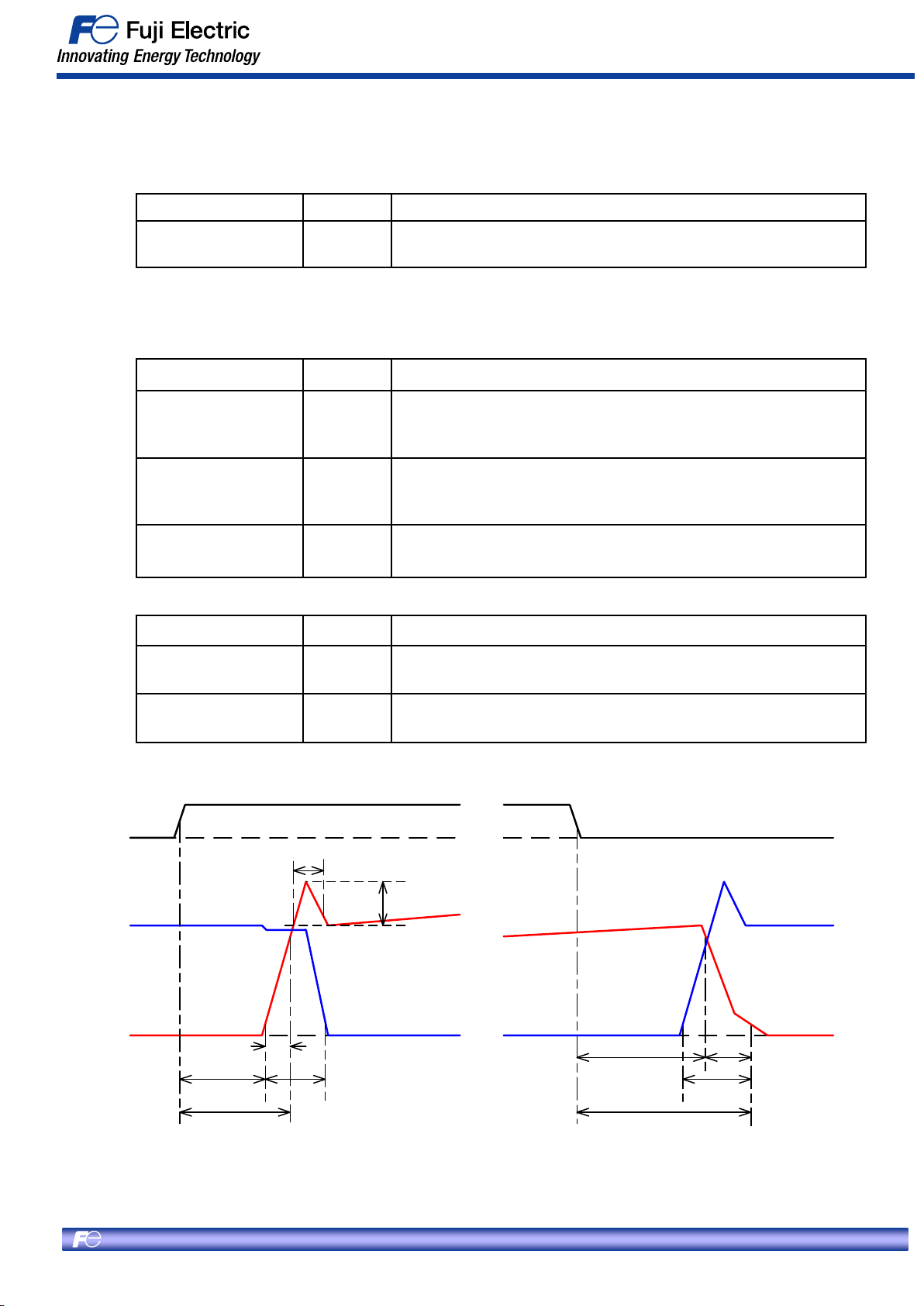
Turn-on time t
Turn-on delay t
Turn-on rise time t
VCE-IC Cross time of turn-on t
Turn-off time t
Turn-off delay t
Turn-on fall time t
I
CES
V
CE(sat)
V
F
on
d(on)
r
c(on)
off
d(off)
f
Collector current when a specified voltage is applied between the collector and
emitter of an IGBT with all input signals L (=0V)
Collector-emitter voltage at a specified collector current when the input signal of
only the element to be measured is H (= 5V) and the inputs of all other elements
are L (=0V)
Forward voltage at a specified forward current with all input signals L (=0V)
The time from the input signal rising above the threshold value until the collector
current becomes 90% of the rating. See Fig. 2-1.
The time from the input signal rising above the threshold value until the collector
current decreases to 10% of the rating. See Fig. 2-1.
The time from the collector current becoming 10% at the time of IGBT turn-on
until the collector current becomes 90%. See Fig. 2-1.
The time from the collector current becoming 10% at the time of IGBT turn-on
until the VCE voltage of IGBT dropping below 10% of the rating. See Fig. 2-1.
The time from the input signal dropping below the threshold value until the VCE
voltage of IGBT becomes 90% of the rating. See Fig. 2-1.
The time from the input signal dropping below the threshold value until the
collector current decreases to 90%. See Fig. 2-1.
The time from the collector current becoming 90% at the time of IGBT turn-off
until the collector current decreases to 10%. See Fig. 2-1.
VCE-IC Cross time of turn-off t
FWD
Reverse recovery time
c(off)
t
rr
The time from the VCE voltage becoming 10% at the time of IGBT turn-off until
the collector current dropping below 10% of the rating. See Fig. 2-1.
The time required for the reverse recovery current of the built-in diode to
disappear. See Fig. 2-1.
(2) Control circuit block
Item Symbol Description
Circuit current of
Low-side drive IC
Circuit current of
High-side drive IC
Circuit current of Bootstrap
circuit
Input Signal threshold
voltage
Input Signal threshold
hysteresis voltage
Operational input pulse
width
I
CCL
I
CCH
I
CCHB
V
th(on)
V
th(off)
V
th(hys)
t
IN(on)
Current flowing between control power supply V
Current flowing between control power supply V
Current flowing between upper side IGBT bias voltage supply VB(U) and
U,VB(V) and V or VB(W) and W on the P-side (per one unit)
Control signal voltage when IGBT changes from OFF to ON
Control signal voltage when IGBT changes from ON to OFF
The hysteresis voltage between V
Control signal pulse width necessary to change IGBT from OFF to ON.
Refer Chapter 3 section 4.
th(on)
and V
th(off)
and COM
CCL
and COM
CCH
.
Operational input pulse
width
Fuji Electric Co., Ltd.
MT6M12343 Rev.1.0
Dec.-2016
t
IN(off)
Control signal pulse width necessary to change IGBT from ON to OFF.
Refer Chapter 3 section 4.
2-3
Page 15

Chapter 2
Description of Terminal Symbols and Terminology
Table 2-2 Description of Terminology
(2) Control circuit block (Continued)
Item Symbol Description
Input current I
Input pull-down resistance R
Fault output voltage
Fault output pulse width t
Over current protection
voltage level
Over Current Protection
Trip delay time
Output Voltage of
temperature sensor
Overheating protection
temperature
Overheating protection
hysteresis
Vcc Under voltage trip level of
Low-side
Vcc Under voltage reset level
of Low-side
IN
IN
V
FO(H)
V
FO(L)
FO
V
IS(ref)
t
d(IS)
V
(temp)
T
OH
T
OH(hys)
V
CCL(OFF)
V
CCL(ON)
Current flowing between signal input IN(HU,HV,HW,LU,LV,LW) and COM.
Input resistance of resistor in input terminals IN(HU,HV,HW,LU,LV,LW).
They are inserted between each input terminal and COM.
Output voltage level of VFO terminal under the normal operation (The lower side arm
protection function is not actuated.) with pull-up resistor 10k
W.
Output voltage level of VFO terminal after the lower side arm protection function is
actuated.
Period in which an fault status continues to be output (VFO) from the VFO terminal
after the lower side arm protection function is actuated. Refer chapter 3 section 6.
Threshold voltage of IS terminal at the over current protection.
Refer chapter 3 section 5.
The time from the Over current protection triggered until the collector current
becomes 50% of the rating. Refer chapter 3 section 5.
The output voltage of temp. It is applied to the temperature sensor output model.
Refer chapter 3 section 7.
Tripping temperature of over heating. The temperature is observed by LVIC.
All low side IGBTs are shut down when the LVIC temperature exceeds overheating
threshold. See Fig.2-2 and refer chapter 3 section 8.
Hysteresis temperature required for output stop resetting after protection operation.
See Fig.2-2 and refer chapter 3 section 8.
TOH and T
are applied to the overheating protection model.
OH(hys)
Tripping voltage of the Low-side control IC power supply.
All low side IGBTs are shut down when the voltage of V
drops below this threshold.
CCL
Refer chapter 3 section 1.
Resetting threshold voltage from under voltage trip status of V
CCL
.
Refer chapter 3 section 1.
Vcc Under voltage hysteresis
of Low-side
Vcc Under voltage trip level of
High-side
Vcc Under voltage reset level
of High-side
Vcc Under voltage hysteresis
of High-side
VB Under voltage trip level V
VB Under voltage reset level V
VB Under voltage hysteresis V
Fuji Electric Co., Ltd.
MT6M12343 Rev.1.0
Dec.-2016
V
CCL(hys)
V
CCH(OFF)
V
CCH(ON)
V
CCH(hys)
B(OFF)
B(ON)
B(hys)
Hysteresis voltage between V
CCL(OFF)
and V
CCL(ON)
.
Tripping voltage of High-side control IC power supply.
The IGBTs of high-side are shut down when the voltage of V
drops below this
CCH
threshold. Refer chapter 3 section 1.
Resetting threshold voltage from under voltage trip status of V
.
See Fig.3-3
CCH
Resetting voltage at which the IGBT performs shut down when the High-side control
power supply voltage V
Hysteresis voltage between V
drops. Refer chapter 3 section 1.
CCH
CCH(OFF)
and V
CCH(ON)
.
Tripping voltage in under voltage of VB(*). The IGBTs of high-side are shut down
when the voltage of VB(*) drops below this threshold. Refer chapter 3 section 2.
Resetting voltage at which the IGBT performs shut down when the upper side arm
IGBT bias voltage VB(*) drops. Refer chapter 3 section 2.
Hysteresis voltage between V
B(OFF)
and V
B(ON)
.
2-4
Page 16
Description of Terminal Symbols and Terminology
Table 2-2 Description of Terminology
(3) BSD block
Item Symbol Description
Chapter 2
Forward voltage of
Bootstrap diode
V
F(BSD)
BSD Forward voltage at a specified forward current.
(4) Thermal Characteristics
Item Symbol Description
Junction to Case Thermal
Resistance
R
th(j-c)_IGBT
Thermal resistance from the junction to the case of a single IGBT.
(per single IGBT)
Junction to Case Thermal
Resistance
R
th(j-c)_FWD
Thermal resistance from the junction to the case of a single FWD.
(per single FWD)
Case to Heat sink
Thermal Resistance
R
th(c-f)
Thermal resistance between the case and heat sink, when mounted on a heat
sink at the recommended torque using the thermal compound
(5) Mechanical Characteristics
Item Symbol Description
Tighten torque
-
Screwing torque when mounting the IPM to a heat sink with a specified screw.
Heat-sink side flatness
V
V
2.1V
IN
CE
I
C
10% 10%
t
d(on)
t
on
90%
-
t
rr
90%
t
r
t
c(on)
Flatness of a heat sink side. See Fig.2-3.
V
IN
I
rp
I
C
V
CE
0.8V
90%
10% 10%
t
d(off)
t
off
t
c(off)
t
f
Fig.2-1 Switching waveforms
Fuji Electric Co., Ltd.
MT6M12343 Rev.1.0
Dec.-2016
2-5
Page 17
Chapter 2
Approx.4.5
Approx.0.7
Approx. 7.0
TOP VIEWSIDE VIEW
Heat sink side
Tc measurement position
Temperature sensor position
Approx. 6.3
Description of Terminal Symbols and Terminology
Fig.2-2 The measurement position of temperature sensor and Tc.
Measurement position Measurement position
+ -
+
-
Fuji Electric Co., Ltd.
MT6M12343 Rev.1.0
Dec.-2016
Fig.2-3 The measurement point of heat-sink side flatness.
2-6
Page 18

Chapter 3
Detail of Signal Input/Output Terminals
Contents Page
1. Control Power Supply Terminals V
2. Power Supply Terminals of High Side VB(U,V,W) ................................... 3-6
3. Function of Internal BSDs (Boot Strap Diodes) ........................................ 3-9
4. Input Terminals IN(HU,HV,HW), IN(LU,LV,LW) ....................................... 3-13
5. Over Current Protection Input Terminal IS .............................................. 3-16
6. Fault Status Output Terminal VFO ........................................................... 3-17
7. Temperature Sensor Output Terminal TEMP ........................................... 3-18
8. Over Heating Protection ............................................................... ............. 3-20
CCH,VCCL
,COM ................................... 3-2
Fuji Electric Co., Ltd.
MT6M12343 Rev.1.0
Dec.-2016
3-1
Page 19

Chapter 3
Detail of Signal Input/Output Terminals
1. Control Power Supply Terminals V
1. Voltage Range of control power supply terminals VCCH, VCCL
Please connect a single 15Vdc power supply between VCCH,VCCL and COM terminals for the IPM
control power supply. The voltage should be regulated to 15V 10% for proper operation. Table 3-1
describes the behavior of the IPM for various control supply voltages. A low impedance capacitor and a
high frequency decoupling capacitor should be connected close to the terminals of the power supply.
High frequency noise on the power supply might cause malfunction of the internal control IC or
erroneous fault signal output. To avoid these problems, the maximum amplitude of voltage ripple on the
power supply should be less than 1V/µs.
The potential at the COM terminal is different from that at the N(*)*1 power terminal. It is very important
that all control circuits and power supplies are referred to the COM terminal and not to the N(*)*1
terminals. If circuits are improperly connected, current might flow through the shunt resistor and cause
improper operation of the short-circuit protection function. In general, it is recommended to make the
COM terminal as the ground potential in the PCB layout.
The main control power supply is also connected to the bootstrap circuit which provide a power to
floating supplies for the high side gate drivers.
When high side control supply voltage (VCCH and COM) falls down under VCCH(OFF) (Under Voltage trip
level of high side), only the IGBT which occurred the under voltage condition becomes off-state even
though the input signal is ON condition.
CCH,VCCL
,COM
When low side control supply voltage (VCCL and COM) falls down under VCCL UV level, all lower side
IGBTs become off-state even though the input signal is ON condition.
Table 3-1 Functions versus supply voltage VCCH, VCCL
Control Voltage Range [V] Function Operations
0 ~ 4 The IPM doesn’t operate. UV and fault output are not activated. dV/dt noise
on the main P-N supply might cause malfunction of the IGBTs.
4 ~ 13 The IPM starts to operate. UV is activated, control input signals are blocked
and fault output VFO is generated.
13 ~ 13.5 UV is reset. IGBTs are operated in accordance with the control gate input.
Driving voltage is below the recommended range, so V
switching loss will be larger than that under normal condition and high side
IGBTs can’t operate after VB(*)
to V
13.5 ~ 16.5 Normal operation. This is the recommended operating condition.
16.5 ~ 20 The lower side IGBTs are still operated. Because driving voltage is above
the recommended range, IGBT’s switching is faster. It causes increasing
system noise. And peak short circuit current might be too large for proper
operation of the short circuit protection.
B(ON)
.
*2
initial charging because VB(*) can’t reach
CE(sat)
and the
Over 20 Control circuit in this IPM might be damaged.
*1 N(*) : N(U), N(V), N(W)
*2 VB(*) : VB(U)-U, VB(V)-V,VB(W)-W
Fuji Electric Co., Ltd.
MT6M12343 Rev.1.0
Dec.-2016
If necessary, it is recommended to insert a Zener diode between each pair
of control supply terminals.
3-2
Page 20

Chapter 3
Detail of Signal Input/Output Terminals
2. Under Voltage (UV) protection of control power supply terminals VCCH, VCCL
Fig.3-1 shows the UV protection circuit of high side and low side control supply(VCCH,VCCL). Fig.3-2 and
Fig.3-3 shows the sequence of UV operation of V
CCH
and V
CCL
.
As shown in Fig.3-1, a diode is electrically connected to the V
CCH
, V
and COM terminals. The diode
CCL
is connected to protect the IPM from the input surge voltage. Don’t use the diode for voltage clamp
purpose otherwise the IPM might be damaged.
C3
+
C4
R
Driver
R
Driver
VB ( U , V , W )
P
VB
IGBT ( H )
OUT
U , V , W
U , V , W
OUT
<BSD>
D R
<HVIC>
internal supply
Vcc
V
CCH
GND Vs
V
CCH
UV
R
HV
level
in
shift
<LVIC>
internal supply
Vcc
V
CCL
V
UV
CCL
(OH)
OC
in
Vcc
GND
C1 C2
+
VFO FO
COM N ( U , V , W )
Alarm
timer
Fig.3-1 Control supply of high and low side V
CCH
, V
CCL
IGBT ( L )
UV Circuit
Fuji Electric Co., Ltd.
MT6M12343 Rev.1.0
Dec.-2016
3-3
Page 21

Input signal
V
Supply voltage
CCL
Chapter 3
Detail of Signal Input/Output Terminals
V
CCL(ON)
V
CCL(OFF)
V
CCL(ON)
V
CCL(OFF)
Lower side IGBT
Collector Current
VFO output voltage
tFO
20µs(min.)
<1> <2> <3>
<1> When V
After V
Fig.3-2 Operation sequence of V
is lower than V
CCL
exceeding V
CCL
CCL(ON)
, all lower side IGBTs are OFF state.
CCL(ON)
, the fault output VFO is released (high level).
Under Voltage protection (lower side arm)
CCL
And the LVIC starts to operate, then next input is activated.
UV detected UV detected UV detected
tFO
<4> <3>
V
CCL(ON)
<2> The fault output VFO is activated when V
OFF state.
If the voltage drop time is less than 20µs, the minimum pulse width of the fault output signal is 20µs
and all lower side IGBTs are OFF state regardless of the input signal condition.
<3> UV is reset after tFO and V
After that the LVIC starts to operate from the next input signal.
<4> When the voltage drop time is more than tFO, the fault output pulse width is generated and all lower
side IGBTs are OFF state regardless of the input signal condition during the same time.
Fuji Electric Co., Ltd.
MT6M12343 Rev.1.0
Dec.-2016
exceeding V
CCL
falls below V
CCL
, then the fault output VFO is reset simultaneously.
CCL(ON)
CCL(OFF)
, and all lower side IGBT remains
3-4
Page 22

Input Signal
V
Supply Voltage
CCH
Chapter 3
Detail of Signal Input/Output Terminals
V
CCH(ON)
V
CCH(OFF)
High side IGBT
Collector Current
VFO output voltage: High-level (no fault output)
<1> <2> <3> <2> <3>
<1>
<1> When V
After V
Fig.3-3 Operation sequence of V
is lower than V
CCH
exceeds V
CCH
CCH(ON)
, the upper side IGBT is OFF state.
CCH(ON)
, the HVIC starts to operate from the next input signals.
Under Voltage protection (high side arm)
CCH
The fault output VFO is constant (high level) regardless V
UV detection UV detection
<2> <3>
.
CCH
V
CCH(ON)
<2> After V
falls below V
CCH
But the fault output VFO keeps high level.
<3> The HVIC starts to operate from the next input signal after UV is reset.
Fuji Electric Co., Ltd.
MT6M12343 Rev.1.0
Dec.-2016
CCH(OFF)
, the upper side IGBT remains OFF state.
3-5
Page 23

Chapter 3
Detail of Signal Input/Output Terminals
2. Power Supply Terminals of High Side VB(U,V,W)
1. Voltage range of high side bias voltage for IGBT driving terminals VB(U,V,W)
The VB(*) voltage, which is the voltage difference between VB(U,V,W) and U,V,W, provides the supply
to the HVICs within the IPM. This supply must be in the range of 13.0~18.5V to ensure that the HVICs
can fully drive the upper side IGBTs. The IPM includes UV function for the VB(*) to ensure that the
HVICs do not drive the upper side IGBTs, if the VB(*) voltage drops below a specified voltage (refer to
the datasheet). This function prevents the IGBT from operating in a high dissipation mode. Please note
here, that the UV (under voltage protection) function of any high side section acts only on the triggered
channel without any feedback to the control level.
In case of using bootstrap circuit, the IGBT drive power supply for upper side arms can be composed
of one common power supply with a lower side arm. In the conventional IPM, three independent
insulated power supplies were necessary for IGBT drive circuit of upper side arm.
The power supply of the upper side arm is charged when the lower side IGBT is turned on or when
freewheel current flows the lower side FWD. Table 3-2 describes the behavior of the IPM for various
control supply voltages. The control supply should be well filtered with a low impedance capacitor and a
high frequency decoupling capacitor connected close to the terminals in order to prevent malfunction of
the internal control IC caused by a high frequency noise on the power supply.
When control supply voltage (VB(U)-U,VB(V)-V and VB(W)-W) falls down under UV (Under Voltage
protection) level, only triggered phase IGBT is off-state regardless the input signal condition.
Table 3-2 Functions versus high side bias voltage for IGBT driving VB(*)
Control Voltage Range [V] IPM operations
0 ~ 4 HVICs are not activated. UV does not operate. dV/dt noise on the main P-
N supply might trigger the IGBTs.
4 ~ 12.5 HVICs start to operate. As the UV is activated, control input signals are
blocked.
12.5 ~ 13 UV is reset. The upper side IGBTs are operated in accordance with the
control gate input. Driving voltage is below the recommended range, so
V
and the switching loss will be larger than that under normal
CE(sat)
condition.
13 ~ 18.5 Normal operation. This is the recommended operating condition.
18.5 ~ 20 The upper side IGBTs are still operating. Because driving voltage is
above the recommended rage, IGBT’s switching is faster. It causes
increasing system noise. And peak short circuit current might be too large
for proper operation of the short circuit protection.
Over 20 Control circuit in the IPM might be damaged. It is recommended to insert
a Zener diode between each pair of high side power supply terminals.
Fuji Electric Co., Ltd.
MT6M12343 Rev.1.0
Dec.-2016
3-6
Page 24

Chapter 3
Detail of Signal Input/Output Terminals
2. Under Voltage (UV) protection of high side power supply terminals VB(U,V,W)
Fig.3-4 shows of high side (VB(U)-U,VB(V)-V and VB(W)-W) UV (Under Voltage protection) circuit
block of the control power supply.
Fig.3-5 shows operation sequence of VB(U)-U,VB(V)-V,VB(W)-W Under Voltage operation.
As shown in Fig.3-4, diodes are electrically connected to the VB(U,V,W), U,V,W and COM terminals.
These diodes protect the IPM from an input surge voltage. Don’t use these diodes for a voltage clamp
because the IPM might be destroyed if the diodes are used as a voltage clamp.
C 3
+
C 4
Vcc
C 1 C 2
+
< BSD >
VB ( U , V , W )
D R
< HVIC >
V
CCH
Vcc
VB
UV
GND Vs
R
in
Driver
< LVIC >
V
CCL
VFO FO
Vcc
Alarm
timer
GND
COM N ( U , V , W )
V
CCL
OC
UV
U , V , W
P
VB
IGBT ( H )
OUT
U , V , W
OUT
IGBT ( L )
Fuji Electric Co., Ltd.
MT6M12343 Rev.1.0
Dec.-2016
Fig.3-4 Control supply of high side VB(*) UV protection circuit
3-7
Page 25

Input signal
VB(*) supply voltage
Chapter 3
Detail of Signal Input/Output Terminals
V
B(ON)
V
B(OFF)
Collector current
VFO output voltage
<1>
<2> <3>
Fig.3-5 Operation sequence of VB(*)*1 Under voltage protection (upper side arm)
<1> When VB(*) is under V
After VB(*) exceeds V
, the upper side IGBT is OFF state.
B(ON)
, the HVIC starts to operate from the next input signal.
B(ON)
The fault output VFO is constant (high level) regardless VB(*).
V
B(ON)
UV detection UV detection
<2> After VB(*) falls below V
But the fault output VFO keeps high level.
<3> The HVIC starts to operate from the next input signal after UV is reset.
*1 VB(*) : VB(U)-U,VB(V)-V,VB(W)-W
Fuji Electric Co., Ltd.
MT6M12343 Rev.1.0
Dec.-2016
, the upper side IGBT remains OFF state.
B(OFF)
3-8
Page 26

Chapter 3
Vcc
<HVIC>
GND Vs
OUT
VB
IGBT(H)
IGBT(L)
Vcc
C
DR
OFF
ON
<BSD>
COM N(U,V,W)
U,V,W
P
VB(U,V,W)
V
CCH
Detail of Signal Input/Output Terminals
3. Function of Internal BSDs (bootstrap Diodes)
There are several ways in which the VB(*)*1 floating supply can be generated. Bootstrap method is
described here. The boot strap method is a simple and cheap solution. However, the duty cycle and
on-time are limited by the requirement to refresh the charge in the bootstrap capacitor. As show in Fig.
3-6, Fig. 3-8 and Fig. 3-11, the boot strap circuit consists of bootstrap diode and resistor which are
integrated in the IPM and an external capacitor.
1.Charging and Discharging of Bootstrap Capacitor During Inverter Operation
a) Charging operation timing chart of bootstrap capacitor (C)
<Sequence (Fig.3-7) : lower side IGBT is turned on in Fig.3-6>
When lower side IGBT is ON state, the charging voltage
on the bootstrap capacitance V
following equations.
V
= V
– VF – V
C(t1)
V
C(t1)
CC
VCC …… Steady state
CE(sat)
VF : Forward voltage of Boost strap diode (D)
V
: Saturation voltage of lower side IGBT
CE(sat)
R : Bootstrap resistance for inrush current limitation (R)
Ib : Charge current of bootstrap
is calculated by the
C(t1)
– Ib·R …… Transient state
When lower side IGBT is turned off, then the motor current
flows through the free-wheel path of the upper side FWD.
Once the electric potential of Vs rises near to that of P
terminal, the charging of C is stopped, and the voltage of C
gradually declines due to a current consumed by the drive
circuit.
*1 VB(*) : VB(U)-U,VB(V)-V,VB(W)-W
Gate signal of
Upper side IGBT
Gate signal of
Lower side IGBT
Voltage level of
bootstrap capacitor
Vcc
Vs
ON
Spontaneous discharge of C
Fig.3-6 Circuit diagram of charging operation
ON
Declining due to current consumed
V
b(t1)
by drive circuit of the upper side IGBT
Fuji Electric Co., Ltd.
MT6M12343 Rev.1.0
Dec.-2016
Fig.3-7 Timing chart of Charging operation
3-9
Page 27

Chapter 3
Vcc
<HVIC>
GND Vs
OUT
VB
IGBT(H)
IGBT(L)
Vcc
C
DR
OFF
OFF
+
-
<BSD>
COM N(U,V,W)
U,V,W
P
VB(U,V,W)
V
CCH
Detail of Signal Input/Output Terminals
<Sequence (Fig.3-9): Lower side IGBT is OFF and Lower
side FWD is ON (Freewheel current flows) in Fig.3-8 >
When the lower side IGBT is OFF and the lower side FWD
is ON, freewheeling current flows the lower side FWD. The
voltage on the bootstrap capacitance V
the following equations:
V
= V
C(t2)
V
VCC ……Steady state
C(t2)
– VF + V
CC
– Ib·R ……Transient state
F(FWD)
VF : Forward voltage of Boost strap diode (D)
V
: Forward voltage of lower side FWD
F(FWD)
R : Bootstrap resistance for inrush current limitation (R)
Ib : Charge current of bootstrap
When both the lower side IGBT and the upper side IGBT
are OFF, a regenerative current flows continuously through
the freewheel path of the lower side FWD. Therefore the
potential of Vs drops to –VF, then the bootstrap capacitor is
re-charged to restore the declined potential. When the
upper side IGBT is turned ON and the potential of Vs
exceeds VCC, the charging of the bootstrap capacitor stops
and the voltage of the bootstrap capacitor gradually
declines due to current consumed by the drive circuit.
is calculated by
C(t2)
Fig.3-8 Circuit diagram of Charging operation
under the lower side arm FWD is ON
Gate signal of
Upper side IGBT
Gate signal of
Lower side IGBT
Voltage level of
bootstrap capacitor (Vb)
Vs
Fig.3-9 Timing chart of Charging operation under the lower side arm FWD is ON
OFF
ON ON
(FWD:ON) (FWD:ON)
V
b(t2)
(FWD:ON)
ON
Declining due to current consumed
by drive circuit of upper side IGBT
Fuji Electric Co., Ltd.
MT6M12343 Rev.1.0
Dec.-2016
3-10
Page 28

Chapter 3
dV
t
IC
1
b
(min)
bCC
2
VV
dVCR
t
Detail of Signal Input/Output Terminals
2) Setting the bootstrap capacitance and minimum ON/OFF pulse width
The parameter of bootstrap capacitor can be calculated by the following equation:
* t1 : the maximum ON pulse width of the upper side IGBT
* Ib : the drive current of the HVIC (depends on temperature and frequency characteristics)
* dV: the allowable discharge voltage. (see Fig.3-10)
A certain margin should be added to the calculated capacitance.
The bootstrap capacitance is generally selected 2~3 times the value of the calculated result.
The recommended minimum ON pulse width (t2) of the lower side IGBT should be basically determined
such that the time constant C・R will enable the discharged voltage (dV) to be fully charged again during
the ON period.
However, if the control mode only has the upper side IGBT switching (Sequence Fig.3-10), the time
constant should be set so that the consumed energy during the ON period can be charged during the
OFF period.
The minimum pulse width is decided by the minimum ON pulse width of the lower side IGBT or the
minimum OFF pulse width of the upper side IGBT, whichever is shorter.
* R : Series resistance of Bootstrap diode ΔRF(BSD)
* C : Bootstrap capacitance
* dV: the allowable discharge voltage.
*VCC : Voltage of HVICs and LVIC power supply (ex.15V)
*V
: the minimum voltage of the upper side IGBT drive (Added margin to UV. ex. 14V)
b(min)
Gate signal of
Upper side IGBT
t
1
Gate signal of
Lower side IGBT
t
2
dV dV
Voltage level of
bootstrap capacitor (Vb)
Declining due to current consumed
by drive circuit of upper side IGBT
Vs
Fig.3-10 Timing chart of Charging and Discharging operation
Fuji Electric Co., Ltd.
MT6M12343 Rev.1.0
Dec.-2016
3-11
Page 29

Chapter 3
Vcc
<HVIC>
GND Vs
OUT
VB
IGBT(H)
IGBT(L)
Vcc
C
DR
OFF
ON
<BSD>
COM N(U,V,W)
U,V,W
P
VB(U,V,W)
V
CCH
Detail of Signal Input/Output Terminals
3) Setting the bootstrap capacitance for Initial charging
The initial charge of the bootstrap capacitor is required to
start-up the inverter.
The pulse width or pulse number should be large enough
to make a full charge of the bootstrap capacitor.
For reference, the charging time of 10F capacitor
through the internal bootstrap diode is about 2ms.
Fig.3-11 Circuit diagram of initial charging
operation
Main Bus voltage
V
(P-N)
HVICs and LVIC
supply voltage
Vcc
Upper side IGBT
supply voltage
Vb(*)
Gate signal of
Lower side IGBT
Start
PWM
ON
Fig.3-12 Timing chart of initial charging operation
Initial charging time
Fuji Electric Co., Ltd.
MT6M12343 Rev.1.0
Dec.-2016
3-12
Page 30

Chapter 3
1 5 10 15 20
1
10
100
1000
125°c
25°c
Built-in equivalent series resistance: Rs [
]
Forward Voltage: VF [V]
-40°c
Typical BSD Built-in limiting resistance Characteristics
IF=f(VF):80s pulse test
0 5 10 15 20
0.0
0.5
1.0
1.5
2.0
125°c
25°c
Forward Current: IF [A]
Forward Voltage: VF [V]
-40°c
Typical BSD Forward Voltage Drop Characteristics
IF=f(VF):80s pulse test
Detail of Signal Input/Output Terminals
4) BSD built-in limiting resistance characteristic
The BSD has non-linear VF-IF characteristic as shown in Fig. 3-13 because the diode forms a built-in
current limiting resistor in the silicon. The equivalent dc-resistance against the charging voltage is
shown in Fig.3-14.
Fig.3-13 VF-IF curve of boot strap diode
Fuji Electric Co., Ltd.
MT6M12343 Rev.1.0
Dec.-2016
Fig.3-14 Equivalent series resistance of boot strap diode
3-13
Page 31

Chapter 3
Detail of Signal Input/Output Terminals
4. Input Terminals IN(HU,HV,HW), IN(LU,LV,LW)
1. Input terminals Connection
Fig.3-15 shows the input interface circuit between the MPU and the IPM. It is possible that the input
terminals connect directly to the MPU. It should not need the external pull up and down resistors
connected to the input terminals, input logic is active high and the pull down resistors are built in.
The RC coupling at each input (parts shown dotted in Fig.3-15) might change depending on the PWM
control scheme used in the application and the wiring impedance of the application’s PCB layout.
IN ( HU ) , IN ( HV ) , IN ( HW )
MPU
IN ( LU ) , IN ( LV ) , IN ( LW )
COM
Fig.3-15 Recommended MPU I/O Interface Circuit of IN(HU,HV,HW), IN(LU,LV,LW) terminals
Fuji Electric Co., Ltd.
MT6M12343 Rev.1.0
Dec.-2016
3-14
Page 32

Chapter 3
Detail of Signal Input/Output Terminals
2. Input terminal circuit
The input logic of this IPM is active high. This logic has removed the sequence restriction between the
control supply and the input signal during startup or shut down operation. Therefore it makes the
system failsafe. In addition, the pull down resistors are built in to each input terminals in Fig.3-16. Thus,
external pull-down resistors are not needed reducing the required external component. Furthermore, a
3.3V-class MPU can be connected directly since the low input signal threshold voltage.
As shown in Fig.3-16, the input circuit integrates a pull-down resistor. Therefore, when using an
external filtering resistor between the MPU output and input of the IPM, please consider the signal
voltage drop at the input terminals to satisfy the turn-on threshold voltage requirement. For instance,
R=100Ω and C=1000pF for the parts shown dotted in Fig.3-15.
Fig.3-16 shows that the internal diodes are electrically connected to the V
, IN(HU, HV, HW, LU, LV,
CCL
LW) and COM terminals. Please don’t use the diode for a voltage clamp intentionally. When the diode
is used as a voltage clamp, it may damage the IPM.
VB(U,V,W)
< BSD >
V
CCH
IN ( HU )
IN ( HV )
IN ( HW )
V
CCL
IN ( LU )
IN ( LV )
IN ( LW )
<HVIC>
Vcc
IN
GND
<LVIC>
internal supply
Vcc
U
IN
V
IN
W
IN
D R
VB
IGBT ( H )
R
HV
+
-
+
-
Input
Noise
Filter
Input
Noise
Filter
level
shift
Delay
R
Driver
R
Driver
OUT
Vs
U , V , W
OUT
IGBT ( L )
P
U , V , W
COM N ( U , V , W )
Fuji Electric Co., Ltd.
MT6M12343 Rev.1.0
Dec.-2016
GND
Fig.3-16 Input terminals IN(HU,HV,HW), IN(LU,LV,LW) Circuit
3-15
Page 33

Chapter 3
Detail of Signal Input/Output Terminals
3. IGBT drive state versus Control signal pulse width
t
is a recommended minimum turn-on pulse width for changing the IGBT state from OFF to ON, and
IN(ON)
t
is a recommended minimum turn-off pulse width for changing the IGBT state from ON to OFF.
IN(OFF)
Fig.3-17 and Fig.3-18 show IGBT drive state for various control signal pulse width.
state A : IGBT may turn on occasionally, even when the ON pulse width of control signal is less than
minimum t
. Also if the ON pulse width of control signal is less than minimum t
IN(ON)
IN(ON)
and
voltage below -5V is applied between U-COM,V-COM,W-COM , it may not turn off due to
malfunction of the control circuit.
state B : IGBT can turn on and is saturated under normal condition.
state C : IGBT may turn off occasionally, even when the OFF pulse width of control signal is less than
minimum t
. Also if the OFF pulse width of control signal is less than minimum t
IN(OFF)
IN(OFF)
and
voltage below -5V is applied between U-COM, V-COM, W-COM , it may not turn on due to
malfunction of the control circuit.
state D : IGBT can turn fully off under normal condition.
Outside recommended
range
Recommended range
A B
0 Minimum
Out recommended
0
Fuji Electric Co., Ltd.
MT6M12343 Rev.1.0
Dec.-2016
t
IN(ON)
Fig.3-17 IGBT drive state versus ON pulse width of Control signal
range
Recommended range
C D
Minimum
t
IN(OFF)
Fig.3-18 IGBT drive state versus OFF pulse width of Control signal
3-16
Page 34

Chapter 3
Detail of Signal Input/Output Terminals
5. Over Current Protection Input Terminal IS
Over current protection (OC) is a function of detecting the IS voltage determined with the external shunt
resistor, connected to N(*)*1 and COM.
Fig.3-19 shows the over current sensing voltage input IS circuit block, and Fig.3-20 shows the OC
operation sequence.
To prevent the IPM from
unnecessary operations due to
normal switching noise or recovery
current, it is necessary to apply an
external R-C filter (time constant is
approximately 1.5µs) to the IS
terminal. Also the IPM and the shunt
resistor should be wired as short as
possible.
Fig.3-19 shows that the diodes in
the IPM are electrically connected to
the V
, IS and COM terminals.
CCL
They should not be used for voltage
clamp purpose to prevent major
problems and destroy the IPM.
V
CCL
IS
COM
VFO
Fig.3-19 Over current sensing voltage input IS circuit
< LVIC >
Alarm
timer
Ref
V
CCL
(OH)
R
Driver
UV
N ( U , V , W )
+
-
*1 N(*) : N(U), N(V), N(W)
L ower side arm
Input signal
IS input voltage
VFO output voltage
Fig.3-20 Operation sequence of Over Current protection
t
d(IS)
V
IS(ref)
OC detected
> t
(min.)
FO
t
1
t2 t
3
t
4
t1 : IS input voltage does not exceed V
normal operation.
t2 : When IS input voltage exceeds V
t3 : The fault output VFO is activated and all lower side IGBT shut down simultaneously after the over current
protection delay time t
t4 : After the fault output pulse width tFO, the OC is reset. Then next input signal is activated.
Fuji Electric Co., Ltd.
MT6M12343 Rev.1.0
Dec.-2016
, while the collector current of the lower side IGBT is under the
IS(ref)
, the OC is detected.
IS(ref)
. Inherently there is dead time of LVIC in t
d(IS)
d(IS)
.
3-17
Page 35

Chapter 3
0.00
0.02
0.04
0.06
0.08
0.10
0.12
0.14
0.16
0.0 0.2 0.4 0.6 0.8 1.0
IFO[mA]
VFO[V]
10kΩ resistance to 5V pull-up
Detail of Signal Input/Output Terminals
6. Fault Status Output Terminal VFO
As shown in Fig.3-21, it is possible to connect the fault status output VFO terminal directly to the MPU.
VFO terminal is open drain configured, thus this terminal should be pulled up by a resistor of
approximate 10k to the positive side of the 5V or 3.3V external logic power supply, which is the same
as the input signals. It is also recommended that the by-pass capacitor C1 should be connected at the
MPU, and the inrush current limitation resistance R1, which is more than 5k, should be connected
between the MPU and the VFO terminal. These signal lines should be wired as short as possible.
Fault status output VFO function is activated by the UV of V
, OC and OH.
CCL
(OH protection function is applied to “6MBP**XSF060-50”.)
Fig.3-21 shows that the diodes in the IPM are electrically connected to the V
, VFO and COM
CCL
terminals. They should not be used for voltage clamp purpose to prevent major problems and destroy
the IPM.
Fig.3-22 shows the Voltage-current characteristics of VFO terminal at fault state condition. The IFO is
the sink current of the VFO terminal as shown in Fig.3-21.
MPU
R 1
C 1
+ 5 V
10 k
Ω
V
CCL
VFO
COM
< LVIC >
internal supply
Vcc
FO
GND
IFO
Alarm
timer
V
CCL
OC
( OH )
_ UV
Fig.3-21 Recommended MPU I/O Interface Circuit of VFO terminal
Fig.3-22 Voltage-current Characteristics of VFO terminal at the fault state condition
Fuji Electric Co., Ltd.
MT6M12343 Rev.1.0
Dec.-2016
3-18
Page 36

Chapter 3
-40 -25 0 25 50 75 100 125 150
0
1
2
3
4
5
max
typ
Output voltage of temperature sensor: V(temp) [V]
Junction Temperature of LVIC:Tj(LVIC) [°c]
min
Temperature sensor Characteristics
V(temp)=f(Tj);V
CCL=VCCH=VB
(*)=15V
Detail of Signal Input/Output Terminals
7. Temperature Sensor Output Terminal TEMP
As shown in Fig. 3-23, the temperature sensor output TEMP can be connected to MPU directly.
It is recommended that a by-pass capacitor and >10k of inrush current limiting resistor are connected
between the TEMP terminal and the MPU. These signal lines should be wired as short as possible to
each device.
The IPM has a built-in temperature sensor, and it can output an analog voltage according to the LVIC
temperature. This function doesn’t protect the IPM, and there is no fault signal output.
“6MBP**XSF060-50” has built-in overheating protection. If the temperature exceeds TOH, these IPMs
output a fault signal due to the overheating protection function.
A diode is electrically connected between TEMP and COM terminal as shown in Fig. 3-12. The purpose
of the diode is a protection of the IPM from an input surge voltage. Don’t use the diode as a voltage
clamp circuit because the IPM might be damaged.
Fig.3-24 shows the LVIC temperature versus TEMP output voltage characteristics. A Zener diode should
be connected to the TEMP terminal when the power supply of MPU is 3.3V. Fig. 3-25 shows the LVIC
temperature versus TEMP output voltage characteristics with 22kΩ pull-down resistor.
Fig.3-26 shows the operation sequence of TEMP terminal at during the LVIC startup and shut down
conditions.
< LVIC >
Ref
Temperature
signal
VDD internal
power supply
+
TEMP
COM
Fig.3-23 Recommended MPU I/O Interface Circuit of TEMP terminal
MPU
Fig.3-24 LVIC temperature vs. TEMP output
voltage characteristics without pull-down resistor
Fuji Electric Co., Ltd.
MT6M12343 Rev.1.0
Dec.-2016
Fig.3-24 LVIC temperature vs. TEMP output
voltage characteristics with 22kΩ pull-down resistor
3-19
Page 37

V
CCL
voltage
VFO
terminal
voltage
TEMP
terminal
voltage
Chapter 3
Detail of Signal Input/Output Terminals
V
increasing V
CCL
V
t
t
1
2
CCL(ON)
decreasing
CCL
V
CCL(OFF)
t3 t
4
Fig.3-25 Operation sequence of TEMP terminal at the LVIC startup and shut down conditions
t1-t2 : TEMP function is activated when V
exceeds V
CCL
CCL(ON)
. If V
is less than V
CCL
CCL(ON)
, the TEMP
terminal voltage is the same as the clamp voltage.
t2-t3 : TEMP terminal voltage rises to the voltage determined by LVIC temperature. In case the
temperature is clamping operation, the TEMP terminal voltage is the clamp voltage even though
V
is above V
CCL
t3-t4 : TEMP function is reset when V
CCL(ON)
.
falls below V
CCL
CCL(OFF)
. TEMP terminal voltage is the same as
the clamp voltage.
Fuji Electric Co., Ltd.
MT6M12343 Rev.1.0
Dec.-2016
3-20
Page 38

Chapter 3
Detail of Signal Input/Output Terminals
8. Over Heating Protection
The over-heating protection (OH) functions is integrated into “6MBP**XSF060-50”.
The OH function monitors the LVIC junction temperature.
The TOH sensor position is shown in Fig.2-2.
As shown in Fig.3-26, the IPM shut down all lower side IGBTs when the LVIC temperature exceeds TOH.
The fault status is reset when the LVIC temperature drops below T
T
OH
T
OH(hys)
OH
– T
OH(hys)
.
TOH – T
OH(hys)
> t
(min.)
FO
t
1
t
2
Fig.3-26 Operation sequence of the Over Heat operation
t1 : The fault status is activated and all IGBTs of the lower side arm shut down, when LVIC temperature
exceeds case overheating protection (OH) temperature TOH.
t2 : The fault status, which outputs over tFO, is reset and next input signal is activated, when LVIC
temperature falls below TOH – T
which is the case overheating protection hysteresis.
OH(hys)
Fuji Electric Co., Ltd.
MT6M12343 Rev.1.0
Dec.-2016
3-21
Page 39

Chapter 4
Power Terminals
Contents Page
1. Connection of Bus Input terminal and Low Side Emitters...................... 4-2
2. Setting of Shunt Resistor of Over Current Protection ........................... 4-3
Fuji Electric Co., Ltd.
MT6M12343 Rev.1.0
Dec.-2016
4-1
Page 40

Chapter 4
Power Terminals
1. Connection of bus input terminal and low side emitters
In this chapter, the guideline and precautions in circuit design on the power terminals, such as how to
determine the resistance of shunt resistor are explained.
(1) Description of the power terminals
Table 4-1 shows the detail about the power terminals.
Table 4-1 Detail description of power terminals
Terminal Name Description
P Positive bus voltage input
It is internally connected to the collector of the high-side IGBTs.
In order to suppress the surge voltage caused by the wiring or PCB pattern
inductance of the bus voltage, connect a snubber capacitor close to this pin.
(Typically metal film capacitors are used)
U,V,W Motor output terminal
Inverter output terminals for connecting to motor load.
N(U),N(V),N(W) Negative bus voltage input terminals
These terminals are connected to the low-side IGBT emitter of the each phase.
In order to monitor the current on each phase, shunt resistors are inserted between
these terminals and the negative bus voltage input (power ground).
(2) Recommended wiring of shunt resistor and snubber capacitor
External current sensing resistors are applied to detect OC (over current) condition or phase currents.
A long wiring patterns between the shunt resistor and the IPM will cause excessive surge that might
damage internal IC, and current detection components. To reduce the pattern inductance, the wiring
between the shunt resistors and the IPM should be as short as possible.
As shown in the Fig.4-1, snubber capacitors should be connected at the right location to suppress
surge voltage effectively. Generally a 0.1 ~ 0.22 F snubber is recommended. If the snubber capacitor
is connected at the wrong location "A" as shown in the Fig.4-1, the snubber capacitor cannot suppress
the surge voltage effectively because inductance of wiring is not negligible.
If the capacitor is connected at the location
"B", the charging and discharging currents
generated by wiring and the snubber capacitor
will appear at the shunt resistor. This will
impact the current sensing signal and the OC
protection level will be lower than the
inductance of wire(or pattern of PCB)
P
DC Bus
Positive
calculated design value. Although the
B
suppression effect when the snubber capacitor
is connected at location "B" is greater than
C
A
+
Bulk Capacitor
location "A" or "C", location "C" is a reasonable
position considering the impact to the current
sensing accuracy. Therefore, location "C" is
recommended.
COM
N(U)
N(V)
N(W)
DC Bus
Negative
Shunt resistor
Fuji Electric Co., Ltd.
MT6M12343 Rev.1.0
Dec.-2016
Fig.4-1 Recommended wiring of shunt resistor
and snubber capacitor
4-2
Page 41

Chapter 4
OC
IS(ref)
Sh
I
V
R
]m[2.11
45
505.0
OC
x)IS(ref)(ma
(min)Sh
I
V
R
PSh
)xIS(ref)(ma
delay
1ln
IR
V
t
d(IS)delaytotal
ttt
Power Terminals
2. Setting of Shunt Resistor of Over Current Protection
(1) Selecting current sensing shunt resistor
The value of current sensing resistor is calculated by the following equation:
(4.1)
Where V
current of OC detection level. V
And RSh is the Resistance of the shunt resistor.
The maximum value of OC level should be set lower than the repetitive peak collector current in the
spec sheet of this IPM considering the tolerance of shunt resistor.
For example, if OC level is set at 45A, the recommended value of the shunt resistor is calculated as:
Where R
Based on above expressions, the minimum shunt resistance of shunt resistor is calculated.
It should be noted that a proper resistance should be chosen considering OC level required in practical
application.
(2) Filter delay time setting of over current protection
An external RC filter is necessary in the over current sensing circuit to prevent unnecessary over
current protection caused by noise. The RC time constant is determined by the applying time of noise
and the short circuit withstand capability of IGBTs. It is recommended to be set approximately 1.5s.
is the Over current protection (OC) reference voltage level of the IPM and IOC is the
IS(ref)
is 0.455V(min.), 0.48V(typ.) and 0.505V(max.).
IS(ref)
(4.2)
is the minimum resistance of the shunt resistor.
Sh(min)
When the voltage across the shunt resistor exceeds the OC level, the filter delay time (t
delays the rises of input voltage of IS terminal to the OC level is caused by the RC filter delay time
constant and is given by:
Where is the RC time constant, IP is the peak current flowing through the shunt resistor.
In addition, there is a shut down propagation delay t
Therefore, the total time t
The short circuit withstands capability of IGBT must be considered for the total delay time t
Please confirm the proper delay time in actual equipment.
Fuji Electric Co., Ltd.
MT6M12343 Rev.1.0
Dec.-2016
) that
delay
(4.3)
of OC.
d(IS)
from OC triggered to shut down of the IGBT is given by:
total
(4.4)
.
total
4-3
Page 42

Chapter 5
Recommended wiring and layout
Contents Page
1. Examples of Application Circuits......................................................... 5-2
2. Recommendation and Precautions in PCB design............................. 5-5
Fuji Electric Co., Ltd.
MT6M12343 Rev.1.0
Dec.-2016
5-1
Page 43

Chapter 5
R2
C2
R1
C3C3C3
ZD1ZD1ZD1
C5
10kΩ
+5V
Vcc
GND
MPU
ZD2
15V
M
C6
D1
C1
C1
C4 C4 C4
Ns
VB(U)
11
10
9
5
3
21
20
19
18
17
16
15
14
13
12
22
23
24
26
28
30
36
32
U
P
V
W
N(V)
N(U)
N(W)
Vcc
IN
GND
OUT
Vs
Vcc
U
IN
V
IN
W
IN
U
OUT
V
OUT
W
OUT
Fo
IS
GND
VFO
IS
COM
COM
IN(LU)
IN(LV)
IN(LW)
V
CCL
V
CCH
IN(HU)
IN(HV)
IN(HW)
VB(V)
VB(W)
TEMP
NC
V
B
7
TEMP
Vcc
IN
GND
OUT
Vs
V
B
Vcc
IN
GND
OUT
Vs
V
B
3×HVIC
LVIC
3×BSD
6×IGBT 6×FWD
Recommended wiring and layout
1. Examples of Application Circuits
In this chapter, recommended wiring and layout are explained
In this section, tips and precautions in PCB design are described with example of application circuit.
Fig. 5-1 and Fig.5-2 show examples of application circuits and their notes.
In these figures, although two types of current detection method are shown, the notes are common.
Bootstrap negative
electrodes should be
connected to U,V,W
terminals directly and
separated from the main
output wires
Fuji Electric Co., Ltd.
MT6M12343 Rev.1.0
Dec.-2016
<C>
Long GND wiring
here might
generate noise to
input and cause
IGBT malfunction.
(In case of sensing all 3 phase currents at once with a single shunt resistor)
<A>
Fig. 5-1 Example of application circuit 1
<B>
Bus voltage
(positive)
Bulk
capacitor
Bus voltage
(negative)
Long wiring here
might cause short
circuit failure,
wiring inductance
should be less
than 10nH.
Long wiring here
might cause OC level
fluctuation and
malfunction.
5-2
Page 44

Chapter 5
Vref=V
IS(ref)
R2
R2
R2
C2
C2
C2
COMP
COMP
COMP
OR
R1
R1
R1
C3C3C3
ZD1ZD1ZD1
C5
10kΩ
+5V
Vcc
GND
MPU
ZD2
15V
M
C6
C1
C1
C4 C4 C4
Ns
VB(U)
11
10
9
5
3
21
20
19
18
17
16
15
14
13
12
22
23
24
26
28
30
36
32
U
P
V
W
N(V)
N(U)
N(W)
Vcc
IN
GND
OUT
Vs
Vcc
U
IN
V
IN
W
IN
U
OUT
V
OUT
W
OUT
Fo
IS
GND
VFO
IS
COM
COM
IN(LU)
IN(LV)
IN(LW)
V
CCL
V
CCH
IN(HU)
IN(HV)
IN(HW)
VB(V)
VB(W)
TEMP
NC
V
B
7
TEMP
Vcc
IN
GND
OUT
Vs
V
B
Vcc
IN
GND
OUT
Vs
V
B
3×HVIC
LVIC
3×BSD
6×IGBT 6×FWD
D1
D1
D1
Recommended wiring and layout
Bootstrap negative
electrodes should be
connected to U,V,W
terminals directly and
separated from the main
output wires
Fuji Electric Co., Ltd.
MT6M12343 Rev.1.0
Dec.-2016
Long GND wiring
here might
generate noise to
input and cause
IGBT malfunction.
<A>
Fig. 5-2 Example of application circuit 2
<B>
<B>
<B>
(In case of sensing each phase current individually)
<C>
<C>
<C>
Long wiring here
might cause short
circuit failure,
wiring Inductance
should be less
than 10nH.
Long wiring here
might cause OC
level fluctuation and
malfunction.
Bus voltage
(positive)
Bulk
capacitor
Bus voltage
(negative)
5-3
Page 45

Chapter 5
Recommended wiring and layout
<Note>
1. Input signal for IGBT driving is High-Active. The input circuit of the IC has a built-in pull-down
resistor. To prevent malfunction, the wiring of each input should be as short as possible. When
using RC filter, please make sure that the input signal level meets the turn-on and turn-off threshold
voltage.
2. The IPM has built-in HVICs and thus it is possible to be connected to a microprocessor (MPU)
directly without any photocoupler or pulse transformer.
3. VFO output is open drain type. It should be pulled up to the positive side of a 5V power supply by a
resistor of about 10kW.
4. To prevent erroneous protection, the wiring of (A), (B), (C) should be as short as possible.
5. The time constant R2-C2 of the protection circuit should be selected approximately 1.5s.
Over current (OC) shut down time might vary due to the wiring pattern. Tight tolerance, tempcompensated type is recommended for R2, C2.
6. It is recommended to set the threshold voltage of the comparator reference input to be same level
as the IPM OC trip reference voltage V
7. Please use high speed type comparator and logic IC to detect OC condition quickly.
8. If negative voltage is applied to R1 during switching operation, connecting a Schottky barrier diode
D1 is recommended.
9. All capacitors should be connected as close to the terminals of the IPM as possible. (C1, C4:
ceramic capacitors with excellent temperature, frequency and DC bias characteristics are
recommended; C3, C5: electrolytic capacitors with excellent temperature and frequency
characteristics are recommended.)
10. To prevent destruction caused by surge voltage, the wiring between the snubber capacitor C6 and P
terminal, Ns node should be as short as possible. Generally, snubber capacity of 0.1F~0.22F is
recommended.
11. Two COM terminals (9 & 16 pin) are connected internally. Please connect either of the terminal to
the signal GND and leave the other terminal open.
12. It is recommended to connect a Zener diode (22V) between each pair of control power supply
terminals to prevent destruction caused by surge voltage.
13. If signal GND is connected to power GND by board pattern, there is possibilty of malfunction due to
fluctuations at the power GND. It is recommended to connect signal GND and power GND at a
single point.
IS(ref)
.
Fuji Electric Co., Ltd.
MT6M12343 Rev.1.0
Dec.-2016
5-4
Page 46

Chapter 5
VB(U)
VB(V)
VB(W)
IN(HU)
IN(HU)
IN(HW)
VCCH
COM
IN(LU)
IN(LV)
IN(LW)
VCCL
VFOISCOM
TEMP
NCPUVW
N(U)
N(V)
N(W)
C
C
C
C
CCR
C
SR
C
R
C
C
C
SGND
SGND
Power
Supply
Power
GND
TO
Motor
ZD
ZD
ZD
from system control,
and power supply for driver IC in IPM
IPM
Power input
Power supply for high side drive
Interface
Over current protection
C
SGND
ZD
Jumper
lead
SBD
C
C
SR
C
slit in PWB
snubber capacitor
shunt resistor
electrolytic capacitor
ceramic capacitor
zener diode
resister
Explanatory notes
PWB pattern
R
Boundary between
high potential difference
C
A
ZD
+-+
-
SBD
C
A
Schottky barrier diode
Recommended wiring and layout
2. Recommendations and Precautions in PCB design
In this section, the recommended pattern layout and precautions in PCB design are described.
Fig.5-3 to Fig.5-7 show the images of recommended PCB layout (referring to example application circuit in
Fig.5-1 and Fig.5-2).
In these figures, the input signals from system control are represented with "IN(HU)".
The recommendations and precautions are as follows,
(1) Overall design around the IPM
(A) Keep a relevant creepage distance at the boundary.
(Place a slit between there if needed.)
(B) The pattern of the power input (DC bus voltage) part and the power supply for high side drive
parts hould be separated in order to prevent the increase of conduction noise.
In case of crossing these wirings on pattern in multi-layer PCB, please take note of stray
capacitance between wires and insulation performance of the PCB.
(C) The pattern of the power supply for high side drive part and the input circuit of each phase part
should be separated to avoid malfunction of the system. In case of using multi-layer PCB, it is
strongly recommended not to cross these wirings.
Details of each part are described in next page.
Fuji Electric Co., Ltd.
MT6M12343 Rev.1.0
Dec.-2016
note) The input signals are represented with "IN(HU)".
Fig.5-3 Image of recommended PCB layout
(Overall design around the IPM)
5-5
Page 47

Chapter 5
To COM terminal
of interface part
NCPUVW
N(W)
SR
C
Power
Supply
Power
GND
IPM
N(V)
N(U)
To IS terminal
VB(U)
VB(V)
VB(W)
U
V
W
C
C
CCC
C
TO
Motor
ZD
ZD
ZD
IPM
Recommended wiring and layout
2. Recommendation and Precautions in PCB design
(2) Power input part
(A) Connect the snubber capacitor between P
terminal and the negative node of the shunt
resistor as close as possible.
The pattern between the snubber capacitor and
P terminal, and shunt resistor should be as
short as possible to avoid the influence of
pattern inductance.
(B) Pattern of the bulk capacitor and snubber
capacitor should be separated near the P
terminal and shunt resistor.
(C) The pattern from power GND and COM
terminal should be connected as close as
possible to the shunt resistor with single-pointgrounding.
(B)
bulk
capacitor
(A)
(D) Please use low inductance shunt resistor.
(E) The pattern between N(U),N(V),N(W) terminals
and the shunt resistor should be as short as
possible.
(3) Power supply for high side drive part.
(A) The pattern between VB(U), VB(V),
VB(W) and the electronic components
(ceramic capacitor, electrolytic capacitor
and Zener diode) should be as short as
possible to avoid the influence of pattern
inductance.
(B) Please use appropriate capacitor
according to applications. Especially,
please use ceramic capacitor or low-ESR
capacitor close to VB(U), VB(V), VB(W)
terminals.
(C) The pattern to Motor output and negative
pole of the capacitor connected to VB(U),
VB(V), VB(W) should be separated close
to U,V and W terminals in order to avoid
malfunction due to common impedance.
(D) (E)
(B)
(C)
Fig.5-4 Image of recommended PCB layout
(Power input part)
(A)
(B)
(C)
(D) If the stray capacitance between VB(U)
and power GND (or equal potential) is
large, the voltage between VB(U) and U
terminals might become overvoltage or
negative voltage when IGBT turns on and
off with high dV/dt. Therefore, connecting
a Zener diode between VB(U) and U are
recommended. It should be connected
close to VB(U) terminal.
(The same applies to VB(V) and VB(W).)
Fuji Electric Co., Ltd.
MT6M12343 Rev.1.0
Dec.-2016
(D)
Fig.5-5 Image of recommended PCB layout
(Power supply for high side drive part)
5-6
Page 48

Recommended wiring and layout
IN(HU)
IN(HU)
IN(HW)
VCCH
COM
IN(LU)
IN(LV)
IN(LW)
VCCL
VFO
IS
COM
TEMP
R
CCC
SGND
SGND
SGND
from system control and
power supply for control IC
To Powe r GND
To Shunt resister
IPM
ZD
C
Jumper
lead
(4) Interface part
(A) Please connect a capacitor between the
input signal and COM terminal if the
influence of noise from the power supply for
high side drive part (and so forth) are not
negligible. The negative pole of the
capacitor should be connected as close as
possible to the pattern of signal GND near
the COM terminal.
If filter resistor or capacitor is used, please
take into account the internal pull down
resistors in this IPM and confirm the signal
level in the actual system.
(B) This IPM has two COM terminals that are
connected internally. Please use either one.
Chapter 5
(A)
(C)
(B)
(C) Electrolytic capacitor and ceramic capacitor
should be connected between V
COM, V
and COM.
CCH
CCL
and
These capacitors should be connected as
close to each terminal as possible.
(D) The output signal from TEMP terminal
should be parallel with Signal GND in order
to minimize the effects of noise.
(E) The pattern of Signal GND from system
control and the pattern from COM terminal
should be connected at single point ground.
The single point ground should be as close
to the COM terminal as possible.
Signal
GND
(SGND)
(E)
(D)
Fig.5-6 Image of recommended PCB layout
(Interface part)
note) The input signals are represented with "IN(HU)".
Fuji Electric Co., Ltd.
MT6M12343 Rev.1.0
Dec.-2016
5-7
Page 49

Chapter 5
Comparator and "OR" logic IC
+
-
V+
V-
+IN
IS
COM
TEMP
N(U)
N(V)
N(W)
C
To Snu bbe r
from system control
IPM
C
SR
SR
To Power GND
SR
C
Voltage supply for
comparator and logic IC
Reference voltage for OC
Jumper
lead
Signal GND of comparator
SBD
R
-IN
IS
COM
TEMP
N(U)
N(V)
N(W)
SRCR
To Power GND
To Snubber
from system control
IPM
SBD
Recommended wiring and layout
(5) Over Current Protection part
As shown in Fig.5-1 and Fig. 5-2, there are 2 methods to sense over current. One is "One-shunt type"
(Fig.5-7 (a)) and the other is "3-shunt type" (Fig.5-7 (b)).
In Fig.5-7 (a)
(A) The pattern between the
negative pole of the shunt
resistor and the COM terminal
is very important.
It is not only the reference zero
level of the control IC, but also
the current path of bootstrap
capacitor charging current and
gate driving current of low side
IGBTs.
Therefore, in order to minimize
the impact of common
impedance, this pattern should
be as short as possible.
(D)
(A)
(a) One-shunt type
(C)
(B)
(A)
(B) The pattern of IS signal should
be as short as possible to avoid
OC level fluctuation and
malfunction.
(C) In order to prevent false
detection during switching
operation, it is recommended to
(B) (C)
connect a RC filter to the IS
terminal. The negative pole of
(b) 3-shunt type
this capacitor should be
connected to the pattern of
signal GND near the COM
Fig.5-7 Image of recommended PCB layout
(Over Current Protection part)
terminal.
(D) If negative voltage is applyid to IS terminal during switching operation, please connect a Schottky
barrier diode between the IS and COM terminals or in parallel with the shunt resistor .
In Fig.5-7 (b)
(A) Please use high speed type comparator and logic IC to detect OC condition quickly.
(B) The reference voltage level of OC which is inputted to the comparator should be coupled by a
capacitor to signal GND. The capacitor should be as close to the comparator as possible.
(C) The pattern of signal GND for COM terminal and the pattern of signal GND for the comparator
should be separated.
(D)
(D) The pattern of signal GND from COM and the pattern of signal GND of the comparator should be
(E) The other precautions and recommendations are same as Fig.5-7 (a).
Please refer to Chapter 4, Section 2 for more information on the circuit constant determination.
Fuji Electric Co., Ltd.
MT6M12343 Rev.1.0
Dec.-2016
connected at single point ground. The single point ground should be as close to the shunt
resistors as possible.
5-8
Page 50

Chapter 6
Mounting Guideline and Thermal Design
Contents Page
1. Soldering to PCB ................................................................................ 6-2
2. Mounting to Heat sink ......................................................................... 6-3
3. Cooler (Heat Sink) Selection............................................................... 6-4
Fuji Electric Co., Ltd.
MT6M12343 Rev.1.0
Dec.-2016
6-1
Page 51

Chapter 6
Mounting Guideline and Thermal Design
1. Soldering to PCB
Soldering
(1) The device temperature during soldering might exceed the maximum storage temperature. To
prevent damage to the device and to ensure reliability, please use the following soldering
temperature.
Table 6.1 Soldering temperature and duration
Methods Soldering Temp. & Time Note
a Solder dipping / Soldering iron 260±5℃, 10±1sec
b Solder dipping / Soldering iron 350±10℃,3.5±0.5sec
(2) The immersion depth of the lead terminal should be more than 1.5mm apart from the device. When
using flow-soldering, be careful to avoid immersing the package in the solder bath.
(3) It is not recommended to reuse the device after it is removed from the circuit board. There is a
possibility that the removed device was subjected to thermal or mechanical damage during the
removal process.
Fuji Electric Co., Ltd.
MT6M12343 Rev.1.0
Dec.-2016
6-2
Page 52

Chapter 6
A
B
DETAIL A DETAIL B
14.0
±0.5
14x2.54 (=35.56)
3.8(min.)
43.0
35.0
16-0.6
8-0.6
18x1.778(=32.004)
±0.5
±0.5
4.2
1.6 ±0.5
±0.5
3.2
±0.5
14.0
14.7
29.4
±0.5
±0.5
±0.5
1.8
1.5
3.7
±0.1
±0.5
0
.
40
2.6
±0.5
10.6
±0.5
1.8±0.1
5.2(min)
2.4
±0.5
1.0 ±0.1
3.2
3.2
±0.5
±0.5
±0.5
5.2
±0.5
±0.54x1.2
1.0
4.5
8.7
±0.5
±0.5
15.6
31.2 ±0.5
±0.5
3579101112131415161718192021
22 23 24 26 28 30 32 36
37
38
39
40
±0.1
Mounting Guideline and Thermal Design
2. Mounting to heat sink
Mounting procedure and precautions
When mounting the IPM to a heat sink, please refer to the following recommended fastening order.
Uneven fastening due to excessive torque might lead to destruction or degradation of the chip.
Recommended:
1 2
Note: the pre-screwing torque is set to 30% of the maximum torque rating.
Fig.6-1 Recommended screw fastening procedure
Pre-screwing: 1 2
Final screwing: 2 1
Fig.6-2 shows the measurement position of heat sink flatness.
The heat sink flatness should be from 0μm/100mm to +100μm/100mm, and the surface roughness (Rz)
should be less than 10 μm.
If the heat sink surface is concave, a gap occurs between the heat sink and the IPM, leading to
deterioration of cooling efficiency.
If the flatness is +100 µm or more, the aluminum base of the IPM is deformed and cracks could occur in
the internal isolating substrates.
In order to obtain effective heat dissipation, thermal compound with good thermal conductivity should be
applied uniformly with +50µm thickness on the contacting surface between the IPM and heat sink.
Refer to the following information for an application position and application quantity.
External heat sink
Fig.6-2 The measurement point of heat sink flatness
-
+
100mm
Center line of
Aluminum base
7.5mm
Fig.6-3 Recommended an application position and application quantity.
Fuji Electric Co., Ltd.
MT6M12343 Rev.1.0
Dec.-2016
Recommended:
Product name : G-747 (Shin-Etsu Silicones)
Application position : 7.5mm apart from the eadge of
aluminum base
7.5mm
Application quantity : 0.03g
Thermal compound
6-3
Page 53

Chapter 6
Mounting Guideline and Thermal Design
3. Cooler (Heat Sink) Selection Method
• Please make sure that the junction temperature Tj should not exceed the maximum junction
temperature T
is always below T
rated load.
for safe operation. Cooling device (heat sink) should be designed to ensures that Tj
j(max)
even during abnormal conditions such as overload operation as well as during
j(max)
• If the IGBT junction temperature is higher than T
The over-heating (OH) protection function works when the IGBT junction temperature exceeds T
, it might cause damage to the chips.
j(max)
j(max)
However, if the temperature rises too quickly, the OH protection might not work.
• Please note that the junction temperature of FWD should not exceed T
j(max)
also.
• When selecting a cooling device (heat sink), please verify the chip temperature by measuring at the
position shown in Figure 2-2.
For more detail about thermal design, please refer Chapter 6 Section 2 of this note and “IGBT
MODULE APPLICATION MANUAL (REH984c)”
Contents:
• Power dissipation loss calculation
• Selecting heat sinks
• Heat sink mounting precautions
• Troubleshooting
.
Fuji Electric Co., Ltd.
MT6M12343 Rev.1.0
Dec.-2016
6-4
Page 54

Chapter 7
Cautions
Contents Page
1. Precautions for use ............................................................................ 7-2
2. Precautions on storage ...................................................................... 7-2
3. Notice ................................................................................................. 7-3
Fuji Electric Co., Ltd.
MT6M12343 Rev.1.0
Dec.-2016
7-1
Page 55

Chapter 7 Cautions
Chapter 7 Cautions
1. Precautions for use
• This IPM should be used within their absolute maximum rating (voltage, current, temperature, etc.). This IPM may be
broken if used beyond the rating.
• Don’t design and use the IPM in excess of the absolute maximum ratings (voltage, current and temperature). The IPM
might be damaged if the IPM is used in excess of the absolute maximum ratings.
• Please refer this Application Manual (MT6M1234) about detailed information for usage, PCB layout, and mounting
instruction.
• The equipment containing this IPM should have adequate fuses or circuit breakers to prevent the equipment from causing
secondary destruction (ex. fire, explosion etc.).
• Please confirm the turn-off current and voltage are within the RBSOA.
• Consider the possible temperature rise not only for the junction and case, but also for the outer leads. Please confirm
these temperatures are within the absolute maximum ratings.
• The IPM is made of incombustible material. However, if the IPM fails, it may emit smoke or flame. When operating the
IPM near any flammable place or material may cause the IPM to emit smoke or flame in case the IPM become even hotter
during operation. Please take measures to prevent the spread of fire.
• Do not touch the leads or package of the IPM directly while power is supplied or during operation in order to avoid electric
shock and burns.
• Connect an appropriate ceramic capacitor between Vcc terminal and gounrd to prevend high frequency noise such as
switching noise.
• The IPM might be damaged when a noise is applied to the control terminals. Please use the IPM after confining the effect
of noise.
• The high-side IGBTs are possibly turned on if the VB voltage reduced to less than V
ceramic capacitors between VB(U) and U terminal, VB(V) and V terminal, VB(W) and W terminal respectively.
• The input signal voltage should be higher than the threshold voltage.
• Use this IPM within their reliability and lifetime under certain environments or conditions. This IPM may fail before the
target lifetime of your products if used under certain reliability conditions. If the IPM is used in excess of the reliability, the
IPM might be broken before the system life time.
• The life time of the semiconductor products is NOT unlimited. Please consider the thermal fatigue caused by temperature
cycle due to self-generated heat. Please use the IPM within the ΔTj power cycle lifetime and ΔTc power cycle lifetime.
The ΔTc power cycle depends on the case temperature (Tc) rise and fall, and the Tc is affected by the cooling conditions
of the system. Please consider the heat generation of the IPM and design the cooling condition to achieve target life time.
• The IPM should not used in an environment in the presence of acid, organic matter, or corrosive gas (hydrogen sulfide,
sulfurous acid gas etc.)
• The IPM may not used in an irradiated environment since they are not radiation-proof.
• It is recommended that any handling of the IPM is done on grounded electrically conductive floor and tablemats.
• Be careful when handling this IPM for ESD damage. (It is an important consideration.)
• When handling the IPM, hold them by the case (package) and don’t touch the leads and terminals.
• Before touching the IPM, discharge any static electricity from your body and clothes by grounding out through a high
impedance resistor (about 1MΩ)
• When soldering, in order to protect the IPM from static electricity, ground the soldering iron or soldering bath through a low
impedance resistor.
• Don’t apply a mechanical force to deforming the terminals.
• During open short test, the internal of the IPM might explode instantaneously and the resin mold package might be blown
off when high voltage is applied to the low voltage terminals. Make sure in your design that during open short test, high
voltage will not be applied to the low terminals. To avoid accidents and explosion damage if high voltage is applied, use
fuses in your design.
. Please connect appropriate
B(off)
Fuji Electric Co., Ltd.
MT6M12343 Rev.1.0
Dec.-2016
7-2
Page 56

Chapter 7 Cautions
2. Precautions on storage
• It is recommended to storage the IPM under the temperature of 5 to 35℃ and relative humidity of 45 to 75%. If the storage
area is very dry, a humidifier may be required. In such a case, use only deionized water or boiled water, since the chlorine
in tap water may corrode the leads.
• The IPM may not be subjected to rapid changes in temperature to avoid condensation on the surface of the IPM. Therefore
store the IPM in a place where the temperature is steady.
• The IPM should not be stored on top of each other, since this may cause excessive external force on the case. When the
IPM stored in packing box, to avoid deformation of the box, please load the box correctly.
• The IPM should be stored with the lead terminals remaining unprocessed. Rust may cause presoldered connections to fail
during later processing.
• The IPM should be stored in antistatic containers or shipping bags.
• Under the above storage condition, the shelf life is one year.
Fuji Electric Co., Ltd.
MT6M12343 Rev.1.0
Dec.-2016
7-3
Page 57

Chapter 7 Cautions
Chapter 7 Cautions
NOTICE
(1) The contents will subject to change without notice due to product specification change or some other reasons. In case of
using the products stated in this document, the latest product specification shall be provided and the data shall be checked.
(2) The application examples in this note show the typical examples of using Fuji products and this note shall neither assure
to enforce the industrial property including some other rights nor grant the license.
(3) Although Fuji Electric Co., Ltd. continually strives to enhance product quality and reliability, a small percentage of
semiconductor products may become faulty. When using Fuji Electric semiconductor products in your equipment, be sure
to take adequate safety measures such as redundant, flame-retardant and fail-safe design in order to prevent a
semiconductor product failure from leading to a physical injury, property damage or other problems.
(4) The product introduced in this Application note is intended for use in the following electronic and electrical equipment
which requires ordinary reliability:
・Inverter for Compressor motor or fan motor for Room Air Conditioner
・Inverter for Compressor motor for heat pump applications.
(5) If you need to use a semiconductor product in this application note for equipment requiring higher reliability than normal,
such as listed below, be sure to contact Fuji Electric Co., Ltd. to obtain prior approval. When using these products, take
adequate safety measures such as a backup system to prevent the equipment from malfunctioning when a Fuji Electric’s
product incorporated in the equipment becomes faulty.
・Transportation equipment (mounted on vehicles and ships)
・Trunk communications equipment ・Traffic-signal control equipment
・Gas leakage detectors with an auto-shutoff function ・Disaster prevention / security equipment
・Safety devices, etc.
(6) Do not use a product in this application note for equipment requiring extremely high reliability
such as:
・Space equipment ・Airborne equipment ・Atomic control equipment
・Submarine repeater equipment ・Medical equipment
(7) All rights reserved. No part of this application note may be reproduced without permission in writing from Fuji Electric Co.,
Ltd.
(8) If you have any question about any portion of this application note, ask Fuji Electric Co., Ltd. or its sales agencies. Neither
Fuji Electric Co., Ltd. nor its agencies shall be liable for any injury or damage caused by any use of the products not in
accordance with instructions set forth herein.
Fuji Electric Co., Ltd.
MT6M12343 Rev.1.0
Dec.-2016
7-4
 Loading...