

Page 1
http://www.fujielectric.com/products/semiconductor/
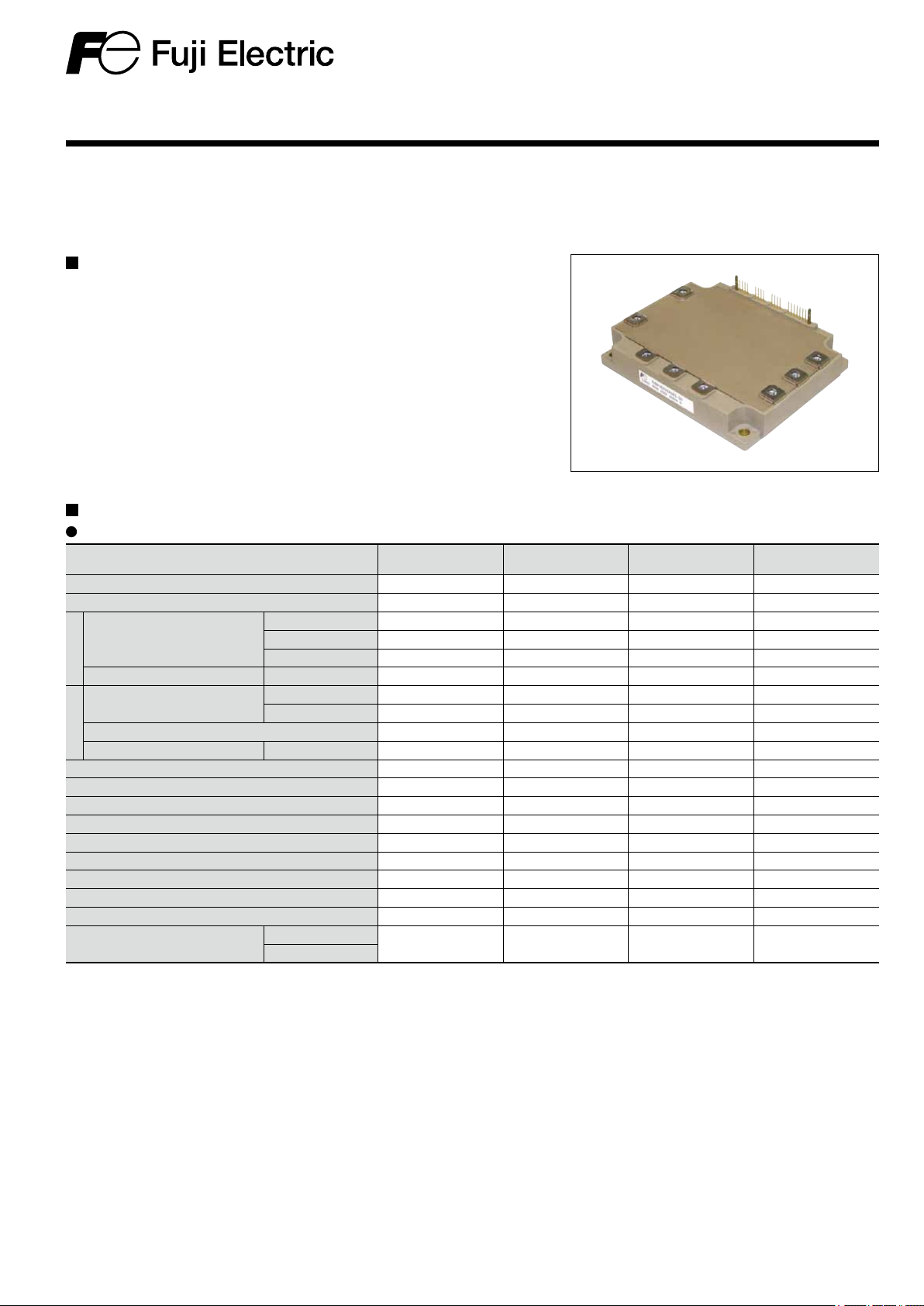
6MBP200VEA060-50
IGBT Modules
IGBT MODULE (V series)
600V / 200A / IPM
Features
• Temperature protection provided by directly detecting
the junction temperature of the IGBTs
• Low power loss and soft switching
• High performance and high reliability IGBT with overheating
protection
• Higher reliability because of a big decrease in number of
parts in built-in control circuit
Maximum Ratings and Characteristics
Absolute Maximum Ratings (TC=25°C, VCC=15V unless otherwise specied)
Items Symbol Min. Max. Units
Collector-Emitter Voltage (*1) V
Short Circuit Voltage V
DC I
Collector Current
Inverter
Collector Power Dissipation 1 device (*3) P
Collector Current
Forward Current of Diode I
Brake
1ms I
Duty=88.6% (*2) -I
DC I
1ms I
Collector Power Dissipation 1 device (*3) P
Supply Voltage of Pre-Driver (*4) V
Input Signal Voltage (*5) V
Alarm Signal Voltage (*6) V
Alarm Signal Current (*7) I
Junction Temperature T
Operating Case Temperature T
Storage Temperature T
Solder Temperature (*8) T
Isolating Voltage (*9) V
Screw Torque
Note *1: VCES shall be applied to the input voltage between all Collector and Emitter.
[ P1-(U,V,W,B) , P2-(U,V,W,B) , (U,V,W,B)-N1 , (U,V,W,B)-N2 ]
Note *2: Duty=125°C/R
Note *3: P
Note *4: V
Note *5: V
Note *6: V
Note *7: I
Note *8: Immersion time 10±1sec. 1 time
Note *9: Terminal to base, 50/60Hz sine wave 1min. All terminals should be connected together during the test.
C=125°C/Rt h(j-c)Q (Inver ter & Brake)
CC shall be applied to the input voltage between terminal No.3 and 1, 7 and 5, 11 and 9, 14 and 13.
in shall be applied to the input voltage between terminal No.2 and 1, 6 and 5, 10 and 9, 15~18 and 13.
ALM shall be applied to the voltage between ter minal No.4 and 1, 8 and 5, 12 and 9, 19 and 13.
ALM shall be applied to the input current to terminal No.4, 8, 12 and 19.
th(j- c)D/(IF×VF Max.)×100
Terminal (M5)
Mounting (M5)
CES 0 600 V
SC 200 400 V
C - 200 A
CP - 400 A
C - 200 A
C - 714 W
C - - A
CP - - A
F - - A
C - - W
CC -0.5 20 V
in -0.5 VCC+0.5 V
ALM -0.5 VCC V
ALM - 20 mA
j - 150 °C
opr -20 110 °C
stg -40 125 °C
sol - 260 °C
iso - AC2500 Vrms
- - 3.5 Nm
1
1442a
MARCH 2014
Page 2
6MBP200VEA060-50
3
IGBT Modules
http://www.fujielectric.com/products/semiconductor/
Electrical Characteristics (Tj=25°C, VCC=15V unless otherwise specied)
Items Symbol Conditions Min. Typ. Max. Units
Collector Current at off signal input I
Collector-Emitter saturation voltage (*10) V
Inverter
Forward voltage of FWD (*10) V
Collector Current at off signal input I
Collector-Emitter saturation voltage (*10) V
Brake
Forward voltage of FWD (*10) V
Switching time
CES VCE=600V - - 1.0 mA
CE(sat) IC=200A
F IF=200A
CES - - - - mA
CE(sat) -
F -
t
on
t
off - - 2.1 µs
t
rr VDC=300V, IF=200A - - 0.3 µs
VDC=300V, Tj=125°C, IC=200A
Terminal - - 1.80 V
Chip - 1.25 - V
Terminal - - 2.35 V
Chip - 1.80 - V
- - - V
- - - V
- - - V
- - - V
1.1 - - µs
Supply current of P-side pre-driver (per one unit) I
Supply current of N-side pre-driver I
Input signal threshold voltage
Over Current Protection
Level
Inverter
Brake - - - A
Over Current Protection Delay time t
Short Circuit Protection Delay time t
IGBT Chips Over Heating Protection Temperature Level T
Over Heating Protection Hysteresis T
Under Voltage Protection Level V
Under Voltage Protection Hysteresis V
Alarm Signal Hold Time
Resistance for current limit R
ccp
ccn - - 78 mA
V
inth(on)
V
inth(off ) OFF 1.5 1.7 1.9 V
I
OC Tj=125°C
dOC Tj=125°C - 5 - µs
SC Tj=125°C - 2 3 µs
jOH Surface of IGBT Chips 150 - - °C
jH - 20 - °C
UV 11.0 - 12.5 V
H 0.2 0.5 - V
t
ALM(OC)
t
ALM(UV ) VCC 10V 2.5 4.0 4.9 ms
t
ALM(Tj OH) 5.0 8.0 11.0 ms
ALM 960 1265 1570 Ω
Switching Frequency= 0-15kHz
TC=-20~110°C
Vin-GND
ON 1.2 1.4 1.6 V
ALM-GND
TC=-20~110°C
- - 26 mA
300 - - A
1.0 2.0 2.4 ms
Note *10: The Ma x value is a case where it measures from P2-(U,V,W,B) , (U,V,W,B)-N2.
Thermal Characteristics (TC = 25ºC)
Items Symbol Min. Typ. Max. Units
Inverter
Junction to Case Thermal Resistance (*11)
Brake
IGBT R
FWD R
IGBT R
FWD R
Case to Fin Thermal Resistance with Compound R
Note *11: For 1device, the measurement point of the case is just under the chip.
th(j- c)Q - - 0.175 °C/W
th(j- c)D - - 0.300 °C/W
th(j- c)Q - - - °C/W
th(j- c)D - - - °C/W
th(c-f) - 0.05 - °C/W
Noise Immunity (VDC=300V, VCC =15V)
Items Conditions Min. Typ. Max. Units
Common mode rectangular noise
Pulse width 1μs, polarity ±10 min.
Judge : no over-current, no miss operating
±2.0 - - kV
Recommended Operating Conditions
Items Symbol Min. Typ. Max. Units
DC Bus Voltage V
Power Supply Voltage of Pre-Driver V
Switching frequency of IPM f
Arm shoot through blocking time for IPM's input signal t
DC - - 400 V
CC 13.5 15.0 16.5 V
SW - - 20 kHz
dead 1.0 - - µs
Screw Torque (M5) - 2.5 - 3.5 Nm
Weight
Items Symbol Min. Typ. Max. Units
Weight W
t - 940 - g
2
Page 3
6MBP200VEA060-50
r
A
A
A
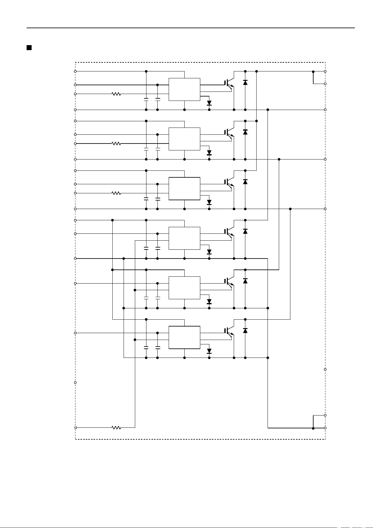
Block Diagram
IGBT Modules
http://www.fujielectric.com/products/semiconductor/
VCCU
VinU
LMU
GNDU
VCCV
VinV
LM V
GNDV
VCCW
VinW
LM W
GNDW
VCC
VinX
③
②
④
①
⑦
⑥
⑧
⑤
⑪
⑩
⑫
⑨
⑭
⑯
P1
Pre-Driver
R
ALM
P2
U
Pre-Driver
R
ALM
V
Pre-Driver
R
ALM
W
Pre-Driver
GND
VinY
VinZ
ALM
⑬
⑰
⑱
⑮
⑲
Pre-Driver
Pre-Driver
B
N1
N2
R
ALM
Pre-drivers include following functions
1. Amplifier for drive
2. Short circuit protection
3. Under voltage lockout circuit
4. Over current protection
5. IGBT chip over heating protection
3
Page 4

6MBP200VEA060-50
5
Characteristics (Representative)
IGBT Modules
http://www.fujielectric.com/products/semiconductor/
Power supply current vs. Switching frequency
j= 25°C(typ.)
T
200
Low-side
High-side
150
100
50
Power supply current : ICC [ mA ]
0
0 5 10 15 20 25
Switchig frequency : f
sw [ kHz ]
Under voltage vs. Junction temperature (typ.)
15
VCC=17V
CC=15V
V
V
CC=13V
VCC=17V
CC=15V
V
V
CC=13V
Input signal threshold voltage
vs. Power supply voltage (typ.)
3.0
TC=25~125°C
2.5
2.0
1.5
inth(on),Vinth(off) [ V ]
V
1.0
Input signal threshold voltage :
0.5
0.0
12 13 14 15 16 17 18
Power supply voltage : V
Under voltage hysterisis
vs. Junction temperature (typ.)
1
Vinth(off)
Vinth(on)
CC [ V ]
12
9
6
Under voltage : VUV [ V ]
3
0
0 20 40 60 80 100 120 140
Junction temperature : T
j [ °C ]
Alarm hold time vs. Power supply voltage (typ.)
10
tALM(TjOH)
8
6
4
Under voltage hysterisis : VH [ V ]
0.8
0.6
0.4
0.2
0
0 20 40 60 80 100 120 140
Junction temperature : T
j [ °C ]
Over heating characteristics
jOH,TjH vs. VCC (typ.)
T
200
TjOH
150
jH [°C]
100
Alarm hold time : tALM [ msec ]
2
tALM(OC)
0
12 13 14 15 16 17 18
Power supply voltage : V
CC [ V ]
4
OH hysterisis : T
50
Over heating protection : TjOH [°C]
0
12 13 14 15 16 17 18
Power supply voltage : V
TjH
CC [ V ]
Page 5

6MBP200VEA060-50
Inverter
IGBT Modules
http://www.fujielectric.com/products/semiconductor/
Collector current vs. Collector-Emitter voltage
j=25°C[Chip] (typ.)
T
400
VCC=15V
300
VCC=17V
VCC=13V
200
Collector current : IC [ A ]
100
0
0.0 0.5 1.0 1.5 2.0 2.5 3.0 3.5
Collector-Emitter voltage : V
CE [ V ]
Collector current vs. Collector-Emitter voltage
j=125°C[Chip] (typ.)
T
400
VCC=15V
300
VCC=17V VCC=13V
Collector current vs. Collector-Emitter voltage
j=25°C[Terminal] (typ.)
T
400
VCC=15V
300
VCC=17V
VCC=13V
200
Collector current : IC [ A ]
100
0
0.0 0.5 1.0 1.5 2.0 2.5 3.0 3.5
Collector-Emitter voltage : V
CE [ V ]
Collector current vs. Collector-Emitter voltage
j=125°C[Terminal] (typ.)
T
400
VCC=15V
300
VCC=17V
VCC=13V
200
Collector current : IC [ A ]
100
0
0.0 0.5 1.0 1.5 2.0 2.5 3.0 3.5
Collector-Emitter voltage : V
CE [ V ]
Forward current vs. Forward voltage
[Chip] (typ.)
400
Tj=125
300
°C
Tj=25
°C
200
Forward current : IF [ A ]
100
200
Collector current : IC [ A ]
100
0
0.0 0.5 1.0 1.5 2.0 2.5 3.0 3.5
Collector-Emitter voltage : V
CE [ V ]
Forward current vs. Forward voltage
[Terminal] (typ.)
400
Tj=125
°C
300
Tj=25
200
Forward current : IF [ A ]
100
°C
0
0.0 0.5 1.0 1.5 2.0 2.5 3.0 3.5
Forward voltage : V
F [ V ]
0
0.0 0.5 1.0 1.5 2.0 2.5 3.0 3.5
Forward voltage : V
F [ V ]
5
Page 6

6MBP200VEA060-50
7
IGBT Modules
http://www.fujielectric.com/products/semiconductor/
Switching Loss vs. Collector Current (typ.)
DC=300V,VCC=15V,Tj=25°C
V
20
15
10
5
Switching loss : Eon,Eoff,Err [mJ/cycle]
0
0 100 200 300 400
Collector current : IC [ A ]
Reversed biased safe operating area
CC=15V,Tj≦125°C[Main Terminal] (min.)
600
V
500
Eon
Eoff
Err
Switching Loss vs. Collector Current (typ.)
DC=300V,VCC=15V,Tj=125°C
V
20
15
10
5
Switching loss : Eon,Eoff,Err [mJ/cycle]
0
0 100 200 300 400
Collector current : IC [ A ]
Transient thermal resistance (max.)
10
Eon
Eoff
Err
400
C [ A ]
300
200
Collector current : I
RBSOA
(Repetitive pulse)
100
0
0 200 400 600 800
Collector-Emitter voltage : V
CE [ V ]
Power derating for IGBT (max.)
[per device]
800
600
C [ W ]
400
1
0.1
Thermal resistance : Rth(j-c) [ °C/W ]
0.01
0.001 0.01 0.1 1 10
Pulse width : P
W [ sec ]
Power derating for FWD (max.)
[per device]
600
400
FWD
IGBT
200
Collector Power Dissipation : P
0
0 50 100 150
Case Temperature : T
C [ °C ]
200
Collector Power Dissipation : PC [ W ]
0
0 50 100 150
Case Temperature : T
6
C [ °C ]
Page 7

6MBP200VEA060-50
IGBT Modules
http://www.fujielectric.com/products/semiconductor/
10000
1000
100
Switching time : ton,toff,tf [ nsec ]
1000
rr [ nsec ]
100
Switching time vs. Collector current (typ.)
DC=300V,VCC=15V,Tj=25°C
V
ton
toff
tf
10
0 100 200 300 400
Collector current : IC [ A ]
Reverse recovery characteristics (typ.)
rr,Irr vs. If
t
trr Tj=125°C
trr Tj=25°C
Irr Tj=125°C
Irr Tj=25°C
Switching time vs. Collector current (typ.)
DC=300V,VCC=15V,Tj=125°C
V
10000
1000
100
Switching time : ton,toff,tf [ nsec ]
10
0 100 200 300 400
Collector current : IC [ A ]
Over current protection vs. Junction temperature (typ.)
CC=15V
V
1000
800
600
ton
toff
tf
10
Reverse recovery current : Irr [ A ]
Reverse recovery time : t
1
0 100 200 300 400
Outline Drawings, mm
Forward current : IF [ A ]
400
200
Over current protection level : IOC [ A ]
0
0 20 40 60 80 100 120 140
Junction temperature : T
j [ °C ]
Weight: 940g(typ.)
7
Page 8

6MBP200VEA060-50
IGBT Modules
http://www.fujielectric.com/products/semiconductor/
WARNING
1. This Catalog contains the product specications, characteristics, data, materials, and structures as of March 2014.
The contents are subject to change without notice for specication changes or other reasons. When using a product listed in this Catalog, be
sur to obtain the latest specications.
2. A ll applic ations described in this Catalog exemplif y the use of Fuji's products for your reference only. No right or license, either express or
implied, under any patent, copyright, trade secret or other intellectual property right owned by Fuji Electric C o., Ltd. is (or shall be deemed)
granted. Fuji Electric Co., Ltd. makes no representation or warranty, whether express or implied, relating to the infringement or alleged
infringement of other's intellectual propert y rights which may arise from the use of the applications described herein.
3. A lthough Fuji Electric Co., Ltd. is enhancing product qualit y and reliability, a small percentage of semiconductor products may become
faulty. When using Fuji Electric semiconductor products in your equipment, you are requested to take adequate safety measures to prevent
the equipment from causing a physical injur y, re, or other problem if any of the products become faulty. It is rec ommended to make your
design failsafe, ame retardant, and free of malfunction.
4. The products introduc ed in this Catalog are intended for use in the following electronic and electrical equipment which has normal reliabilit y
requirements.
• Computers • OA equipment • Communications equipment (terminal devices) • Measurement equipment
• Machine tools • Audiovisual equipment • Electrical home appliances • Personal equipment • Industrial robots etc.
5. If you need to use a product in this Catalog for equipment requiring higher reliabilit y than normal, such as for the equipment listed below,
it is imperative to cont act Fuji Electric Co., Ltd. to obtain prior approval. W hen using these products for such equipment, take adequate
measures such as a backup system to prevent the equipment from malfunctioning even if a Fuji's product incorporated in the equipment
becomes faulty.
• Transportation equipment (mounted on cars and ships) • Trunk communications equipment
• Trafc-signal control equipment • Gas leakage detector s with an auto -shut- off feature
• Emergency equipment for responding to disasters and anti-burglary devices • Safety devices
• Medical equipment
6. Do not use products in this Catalog for the equipment requiring strict reliability such as the following and equivalents to strategic equipment
(without limitation).
• Space equipment • Aeronautic equipment • Nuclear control equipment
• Submarine repeater equipment
7. Copyright ©1996 -2014 by Fuji Electr ic Co., Ltd. All r ights reserved.
No part of this Catalog may be reproduced in any form or by any means without the express permission of Fuji Electric Co., Ltd.
8. If you have any question about any portion in this Catalog, ask Fuji Electric Co., Ltd. or its sales agents before using the product.
Neither Fuji Electric Co., Ltd. nor its agents shall be liable for any injury caused by any use of the products not in accordance with instructions
set forth herein.
8
Page 9

Technical Information
Please refer to URLs below for futher information about products, application manuals and technical documents.
关于本规格书中没有记载的产品信息,应用手册,技术资料等,请参考以下链接。
本データシートに記載されていない製品情報 , アプリケーションマニュアル , 技術資料は以下の URL をご参照下さい。
IGBT Modules
FUJI ELECTRIC Power Semiconductor WEB site
日本
Global
中国
Europe
North America
www.fujielectric.co.jp/products/semiconductor/
www.fujielectric.com/products/semiconductor/
www.fujielectric.com.cn/products/semiconductor/
www.fujielectric-europe.com/components/semiconductors/
www.americas.fujielectric.com/components/semiconductors/
Information
日本
1
半導体総合カタログ
2
製品情報
3
アプリケーションマニュアル
4
技術資料
5
マウンティングインストラクション
6
IGBT 損失シミュレーションソフト
7
AT-NPC 3-Level 損失シュミレーションソフト
8
富士電機技報
9
製品のお問い合わせ
10
改廃のお知らせ
Global
1
Semiconductors General Catalog
2
Product Information
3
Application Manuals
4
Technical Documents
5
Mounting Instructions
6
IGBT Loss Simulation Software
7
AT-NPC 3-Level Loss Simulation Software www.fujielectric.com/products/semiconductor/model/igbt/simulation_3level/
8
Fuji Electric Journal
9
Contact
10
Revised and discontinued product information www.fujielectric.com/products/semiconductor/discontinued/
www.fujielectric.co.jp/products/semiconductor/catalog/
www.fujielectric.co.jp/products/semiconductor/model/
www.fujielectric.co.jp/products/semiconductor/model/igbt/application/
www.fujielectric.co.jp/products/semiconductor/model/igbt/technical/
www.fujielectric.co.jp/products/semiconductor/model/igbt/mounting/
www.fujielectric.co.jp/products/semiconductor/model/igbt/simulation/
www.fujielectric.co.jp/products/semiconductor/model/igbt/simulation_3level/
www.fujielectric.co.jp/products/semiconductor/journal/
www.fujielectric.co.jp/products/semiconductor/contact/
www.fujielectric.co.jp/products/semiconductor/discontinued/
www.fujielectric.com/products/semiconductor/catalog/
www.fujielectric.com/products/semiconductor/model/
www.fujielectric.com/products/semiconductor/model/igbt/application/
www.fujielectric.com/products/semiconductor/model/igbt/technical/
www.fujielectric.com/products/semiconductor/model/igbt/mounting/
www.fujielectric.com/products/semiconductor/model/igbt/simulation/
www.fujielectric.com/products/semiconductor/journal/
www.fujielectric.com/products/semiconductor/contact/
中国
1
半导体综合目录
2
产品信息
3
应用手册
4
技术资料
5
安装说明书
6
IGBT 损耗模拟软件
7
AT-NPC 3-Level 损耗模拟软件
8
富士电机技报
9
产品咨询
10
产品更改和停产信息
www.fujielectric.com.cn/products/semiconductor/catalog/
www.fujielectric.com.cn/products/semiconductor/model/
www.fujielectric.com.cn/products/semiconductor/model/igbt/application/
www.fujielectric.com.cn/products/semiconductor/model/igbt/technical/
www.fujielectric.com.cn/products/semiconductor/model/igbt/mounting/
www.fujielectric.com.cn/products/semiconductor/model/igbt/simulation/
www.fujielectric.com.cn/products/semiconductor/model/igbt/simulation_3level/
www.fujielectric.com.cn/products/semiconductor/journal/
www.fujielectric.com.cn/products/semiconductor/contact/
www.fujielectric.com.cn/products/semiconductor/discontinued/
2015-10
 Loading...