

Page 1
SPECIFICATION
Device Name :
Type Name :
Spec. No. :
IGBT Module
2MBI400TB-060
MS5F 5293
Oct. 22 '02
Y.Kobayashi
T.Miyasaka
K.Yamada
Fuji Electric Co.,Ltd.
Matsumoto Factory
a
T.FujihiraOct. 23 '02
MS5F 5293
1
14
b
c
H04-004-07
Page 2
R e v i s e d R e c o r d s
Class i-
Date
Oct.-23-'02 T.Fujihira
Nov.-29-'02
Jan.-31-'03
Apr.-07-'04
fication Ind. Content
enactment
Revised Reliab ility
Revision
Revision
Revision
a
test condition (P7/14)
Revised characteristics
b
curve up to 800A
(P11/14, 12/14)
Revised ton,tr,toff,tf
(P4/14)
c
Revised Rth curve
(P12/14)
Applied
date Drawn Checked Approved
Issued
date
Y.Kobayashi
Y.Kobayashi
T.Miyasaka
K.Yamada
T.Miyasaka
K.Yamada
T.Miyasaka
K.Yamada
T.Miyasaka
K.Yamada
T.Fujihira
T.Fujihira
Y.SekiY.Kobayashi
MS5F 5293
a
2
14
b
c
H04-004-06
Page 3
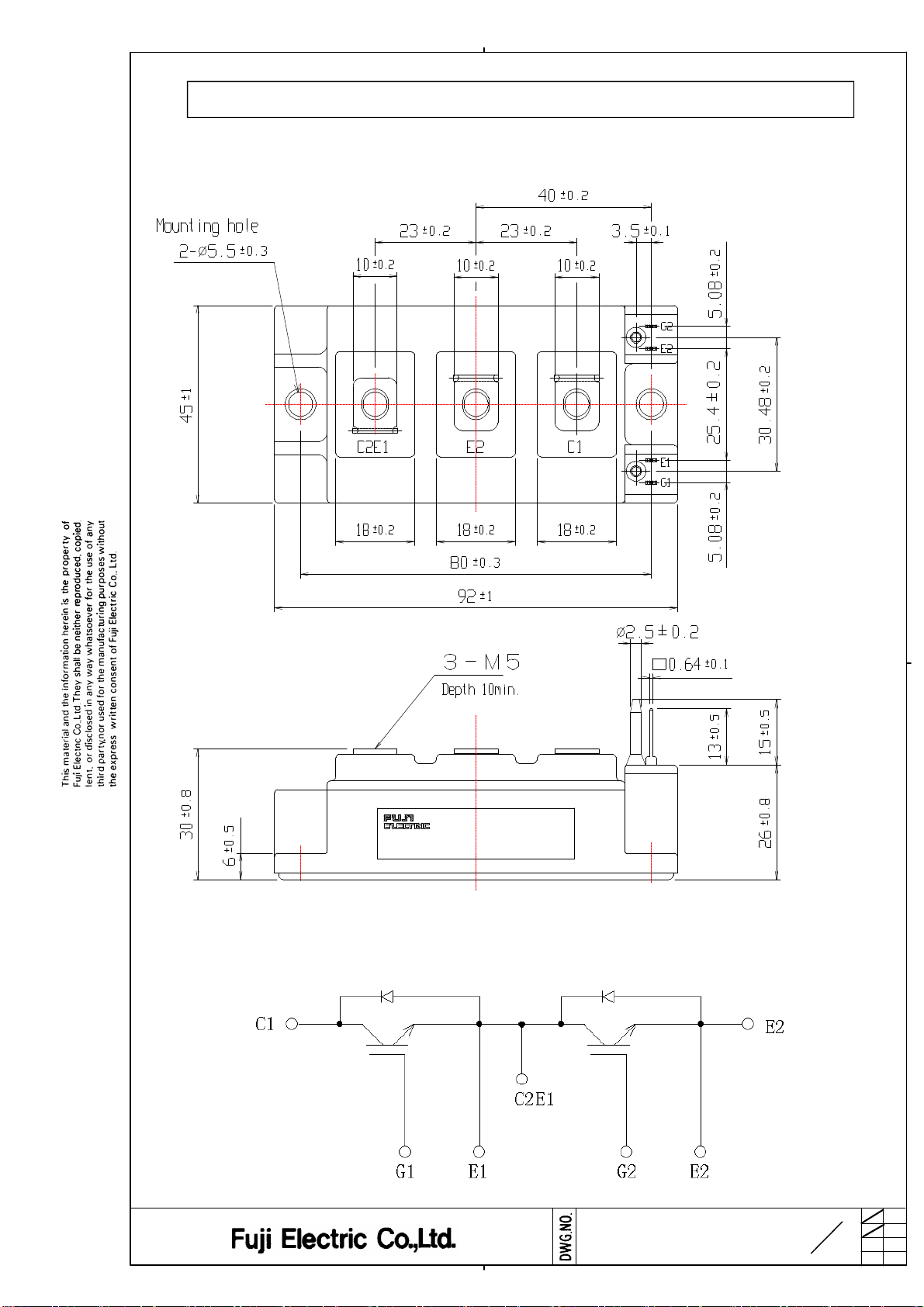
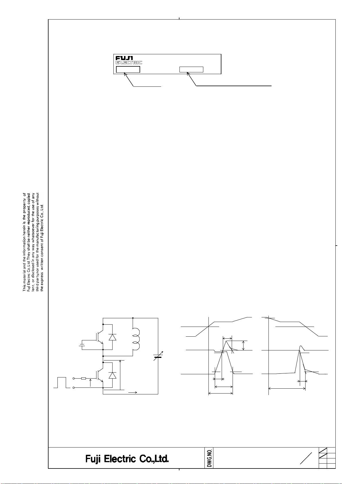
1. Outline Drawing ( Unit : mm )
2MBI400TB-060
2. Equivalent circuit
MS5F 5293
14
a
b
c
3
H04-004-03
Page 4
3. Absolute Maximum Ratings ( at Tc= 25℃ unless otherwise specified
Zero gate voltage
Collector current
Items Symbols Conditions
)
Maximum
Ratings
Collector-Emitter voltage VCES Ic=1mA 600 V
Gate-Emitter voltage VGES ±20 V
Ic Duty=100 %
Collector current Ic pulse 1ms
IF
Duty=56 %
400
800
400
IF pulse 1ms 800
Collector Power Dissipation Pc 1270 W
1 device
Junction temperature Tj 150
Storage temperature Tstg -40~ +125
Isolation voltage
Screw Torque
(*1)
Viso AC : 1min. 2500 V
Mounting
Terminals
(*2)
(*2)
3.5
3.5
(*1) All terminals should be connected together when isolation test will be done.
(*2) Recommendable Value : Mounting 2.5~3.5 Nm (M5)
Terminal 2.5~3.5Nm (M5)
4. Electrical characteristics ( at Tj= 25℃ unless otherwise specified)
Characteristics
Items Symbols Conditions
min. typ. Max.
Units
A
℃
℃
Nm
Units
Gate-Emitter leakage current I
Gate-Emitter
threshold voltage
Collector-Emitter
VCE(sat)
I
CESVGE
GESVCE
V
GE(th)VCE
= 0 V, V
= 0 V, V
= 600 V - - 2.0 mA
CE
= ±20 V - - 400
GE
= 20 V, Ic = 400 mA 6.2 6.7 7.7 V
V
= 15 V Chip - 1.9 -
GE
saturation voltage Ic = 400 A Terminal - 2.2 2.5
Input capacitance Cies
Output capacitance Coes V
VGE =
CE
0 V - 30000 -
= 10 V - 5200 - pF
Reverse transfer capacitance Cres f = 1 MHz - 4500 -
ton Vcc = 300 V -
Turn-on time tr Ic = 400 A -
tr
V
= ±15 V - 0.1 -
GE
(i)
Turn-off time
toff RG = 6.8
tf -
Forward on voltage V
FIF
= 400 A
Chip - 1.75 -
c
c
0.2
c
-
0.55
c
0.05
0.4
1.2
0.6
1.2
0.45
Terminal - 1.9 2.5
Reverse recovery time trr IF = 400 A - - 0.3
Allowabe avalanche energy
during short circuit cutting off P
AV
Ic > 800A, Tj = 125
℃
200 - - mJ
(Non-repetitive)
μ
μ
A
n
V
s
V
s
5. Thermal resistance characteristics
Items Symbols Conditions
Thermal resistance
R
th(j-c)
IGBT - - 0.098
(1 device) FWD - - 0.19℃/
Contact Thermal resistance R
th(c-f)
With thermal compound
* This is the value which is defined mounting on the additional cooling fin
with thermal compound.
※
MS5F 5293
Characteristics
min. typ. Max.
0.025
-
-
H04-004-03
Units
W
a
4
14
b
c
Page 5
6. Indication on module
2MBI400TB-060
400A 600V
Lot No.
7. Applicable category
This specification is applied to IGBT Module named 2MBI400TB-060
8. Storage and transportation notes
The module should be stored at a standard temperature of 5 to 35C and
・
humidity of 45 to 75% .
Store modules in a place with few temperature changes in order to avoid
・
condensation on the module surface.
Avoid exposure to corrosive gases and dust.
・
Avoid excessive external force on the module.
・
Store modules with unprocessed terminals.
・
Place of manufucturing
Do not drop or otherwise shock the modules when tranporting.
・
9. Definitions of switching time
R
G
V
GE
V
CE
~
~
~
90%
0V
Ic
90%
V
CE
t
f
t
off
~
0V
V
L
Vcc
Ic
GE
V
CE
Ic
0V
0A
10%
90%
t
rr
I
rr
~
10% 10%
~
t
r(i)
t
r
t
on
MS5F 5293
a
14
b
c
5
H04-004-03
Page 6

10. Definition of the allowable avalance energy during short circuit cutfing of.
-VCEP
1
PAV=
2
-ICPIC
VCE
tf(SC)
11. UL recognition
×VCEP×ICP×tf(SC)
This products is recognized by Underwriters Laboratories Inc., the file No. is E82988.
12. Packing and Labeling
Packing box
Display on the packing box
- Logo of production
- Type name
- Lot No.
Display
* Each modules are packed with electrical protection.
- Products quantity in a packing box
MS5F 5293
a
14
b
c
6
H04-004-03
Page 7

13. Reliability test results
10G
Atmospheric pressure : 2.03×10
Pa
Used liquid : Water with ice and
boiling water
Reliability Tes t Item s
Test
categories
Mechanical Tests
Test items Test methods and conditions
1 Terminal Strength Pull force :
(Pull test) Test time : 10±1 sec. Method 1
2 Mounting Strength Screw torque : 2.5 ~ 3.5 N・m (M5) A - 112 5 ( 1 : 0 )
Test time : 10±1 sec. Method 2
3 Vibration Range of frequency : 10 ~ 500Hz A - 121 5 ( 1 : 0 )
Sweeping time : 15 min.
Acceleration :
Sweeping direction : Each X,Y,Z axis
Test time : 6 hr. (2hr./direction)
4 Shock Maximum acceleration : 1000G A - 122 5 ( 1 : 0 )
Pulse width : 0.5msec.
Direction : Each X,Y,Z axis
Test time : 3 times/direction
1 High Temperature Storage temp. : 125±5 ℃ B - 111 5 ( 1 : 0 )
Storage Test duration : 1000hr.
2 Low Temperature Storage temp. : -40±5 ℃ B - 112 5 ( 1 : 0 )
Storage Test duration : 1000hr.
3 Temperature Storage temp. : 85±3 ℃ B - 121 5 ( 1 : 0 )
Humidity Relative humidity : 85±5%
Storage Test duration : 1000hr.
4 Unsaturated Test temp. : 121 ℃ B - 123 5 ( 1 : 0 )
Pressure Cooker
Test duration : 20hr.
5 Temperature
Cycle Test temp. :
a
40N
a
5
(Reference value)
Low temp. -40 -5 ℃
High temp. 125 -5 ℃
+3 B - 131 5 ( 1 : 0 )
+5
Reference
norms
EIAJ
ED-4701
A - 111 5 ( 1 : 0 )
Number
of sample
Acceptance
number
Environment Tests
6 Thermal Shock
RT 5 ~ 35 ℃
Dwell time : High ~ RT ~ Low ~ RT
1hr. 0.5hr. 1hr. 0.5hr.
Number of cycles : 100 cycles
Test temp. :
Dipping time : 5 min. par each temp.
Transfer time : 10 sec.
Number of cycles : 10 cycles
High temp. 100 -5
Low temp. 0 -0 ℃
a
+0 B - 141 5 ( 1 : 0 )
+5
℃
MS5F 5293
a
14
b
c
7
H04-004-03
Page 8

wetting tests, for example, moisture resistance tests, each component shall be made wipe or dry
Reliab ility Tes t Items
Test
categories
Endurance Tests
Reference
Test items Test methods and conditions
1 High temperature
Reverse Bias Test temp. :
Bias Voltage : VC = 0.8×VCES
Bias Method : Applied DC voltage to C-E
Test duration : 1000hr.
2 High temperature
Bias Test temp. :
Bias Voltage : VC = VGE = +20V or -20V
Bias Method : Applied DC voltage to G-E
Test duration : 1000hr.
3 Temperature B - 121 5 ( 1 : 0 )
Humidity Bias Test temp. :
Relative humidity :
Bias Voltage : VC = 0.8×VCES
Bias Method : Applied DC voltage to C-E
Test duration : 1000hr.
4 Intermitted ON time : 2 sec. D - 322 5 ( 1 : 0 )
Operating Life OFF time : 18 sec.
(Power cycle) Test temp. :
( for IGBT )
Number of cycles : 15000 cycles
Ta = 125 -5 ℃
(Tj ≦ 150 ℃)
VGE = 0V
Ta = 125 -5
(Tj ≦ 150 ℃)
VCE = 0V
85 +-3oC
85 +-5%
VGE = 0V
Tj=100±5 deg
Tj ≦ 150 ℃, Ta=25±5 ℃
+0
+0
℃
norms
EIAJ
ED-4701
D - 313 5 ( 1 : 0 )
D - 323 5 ( 1 : 0 )
Number
of sample
Acceptance
number
Failure Criteria
Item Characteristic Symbol Failure criteria Unit Note
Lower limit Upper limit
Electrical Leakage current ICES - USL×2 mA
characteristic ±IGES - USL×2
Gate threshold voltage VGE(th) LSL×0.8 USL×1.2 mA
Saturation voltage VCE(sat) - USL×1.2 V
Forward voltage VF - USL×1.2 V
Thermal IGBT
VGE - USL×1.2 mV
resistance or VCE
FWD
VF - USL×1.2 mV
Isolation voltage Viso Broken insulation -
Visual Visual inspection
inspection Peeling - The visual sample -
Plating
and the others
LSL : Lower specified limit.
USL : Upper specified limit.
Note : Each parameter measurement read-outs shall be made after stabilizing the components at room
ambient for 2 hours minimum, 24 hours maximum after removal from the tests. And in case of the
A
completely before the measurement.
MS5F 5293
a
14
b
c
8
H04-004-03
Page 9

Reliability Test Results
Test
cate-
gories
Reference
Test items
1 Terminal Strength A - 111 5 0
(Pull test) Method 1
2 Mounting Strength A - 112 5 0
3 Vibration A - 121 5 0
norms
EIAJ ED-4701
Method 2
Number
of test
sample
Number
of failure
sample
Mechanical Tests
4 Shock A - 122 5 0
1 High Temperature Storage B - 111 5 0
2 Low Temperature Storage B - 112 5 0
3 Temperature Humidity B - 121 5 0
Storage
4 Unsaturated B - 123 5 0
Pressure Cooker
Environment Tests
5 Temperature Cycle B - 131 5 0
6 Thermal Shock B - 141 5 0
1 High temperature Reverse Bias D - 313 5 0
2 High temperature Bias D - 323 5 0
( for gate )
3 Temperature Humidity Bias B - 121 5 0
Endurance Tests
4 Intermitted Operating Life D - 322 5 0
(Power cycling)
( for IGBT )
MS5F 5293
14
a
b9
c
H04-004-03
Page 10

Collector current vs. Collector-Emitter voltage
[ Inverter ]
1000
Tj= 25C (typ.)
Collector current vs. Collector-Emitter voltage
[ Inverter ]
1000
Tj= 125C (typ.)
15V
800
600
400
VGE= 20V
12V
Collector current : Ic [ A ]
200
0
0 1 2 3 4 5
Collector - Emitter voltage : VCE [ V ]
[ Inverter ]
Collector current vs. Collector-Emitter voltage
1000
800
600
VGE=15V (typ.)
Tj= 25C
10V
8V
Tj= 125C
800
600
400
VGE= 20V
Collector current : Ic [ A ]
200
0
0 1 2 3 4 5
Collector - Emitter voltage : VCE [ V ]
[ Inverter ]
Collector-Emitter voltage vs. Gate-Emitter voltage
12
10
8
Tj= 25C (typ.)
15V
12V
10V
8V
400
Collector current : Ic [ A ]
200
0
0 1 2 3 4
Collector - Emitter voltage : VCE [ V ]
[ Inverter ]
Capacitance vs. Collector-Emitter voltage (typ.)
VGE=0V, f= 1MHz, Tj= 25C
Capaci tance : Cies, Coes, Cres [ pF ]
50000
10000
5000
1000
Cies
Coes
Cres
6
4
2
Collector - Emitter voltage : VCE [ V ]
0
5 10 15 20 25
Ic=800A
Ic=400A
Ic=200A
Gate - Emitter voltage : VGE [ V ]
[ Inverter ]
Dynamic Gate charge (typ.)
500
400
300
200
100
Collector - Emitter voltage : VCE [ V ]
Vcc=300V, Ic=400A, Tj= 25C
25
20
15
10
5
Gate - Emitter voltage : VGE [ V ]
500
0 5 10 15 20 25 30 35
Collector - Emitter voltage : VCE [ V ]
0
0 200 400 600 800 1000 1200 1400 1600
Gate charge : Qg [ nC ]
10
MS5F 5293
H04-004-03
0
14
a
b
c
Page 11

b b
Switching time vs. Collector current (typ.)
Vcc=300V, VGE=+-15V, Rg=6.8ohm, Tj= 25C
1000
[ Inverter ]
toff
ton
Switching time vs. Collector current (typ.)
[ Inverter ]
Vcc=300V, VGE=+-15V, Rg= 6.8ohm, Tj= 125C
1000
ton
toff
100
Switching time : ton, tr, toff, tf [ nsec ]
10
0 200 400 600 800 1000
Collector current : Ic [ A ]
[ Inverter ]
Switching time vs. Gate resistance (typ.)
5000
1000
Switching time : ton, tr, toff, tf [ nsec ]
Vcc=300V, Ic=400A, VGE=+-15V, Tj= 25C
ton
toff
tr
100
10
1 10 50
Gate resistance : Rg [ ohm ]
tf
tr
tf
100
tr
tf
Switching time : ton, tr, toff, tf [ nsec ]
10
0 200 400 600 800 1000
Collector current : Ic [ A ]
b
Switching loss vs. Collector current (typ.)
[ Inverter ]
Vcc=300V, VGE=+-15V, Rg=6.8ohm
30
20
10
Switching loss : Eon, Eoff, Err [ mJ/pulse ]
0
0 200 400 600 800 1000
Collector current : Ic [ A ]
Eoff(125C)
Eoff(25C)
Eon(125C)
Eon(25C)
Err(125C)
Err(25C)
Switching loss vs. Gate resistance (typ.)
[ Inverter ]
Vcc=300V, Ic=400A, VGE=+-15V, Tj= 125C
70
60
50
40
30
20
10
Switching loss : Eon, Eoff, Err [ mJ/pulse ]
0
5 10 100
Gate resistance : Rg [ ohm ]
Eon
Eoff
Err
Reverse bias safe operating area
[ Inverter ]
+VGE=15V, -VGE<=15V, Rg>=6.8ohm, Tj<=125C
1000
900
800
700
600
500
400
300
Collector current : Ic [ A ]
200
100
0
0 200 400 600 800
Collector - Emitter voltage : VCE [ V ]
MS5F 5293
11
14
a
b
c
H04-004-03
Page 12

b b
Forward current vs. Forward on voltage (typ.)
900
800
700
600
500
400
300
Forward current : IF [ A ]
200
100
[ Inverter ]
Tj=125C
Tj=25C
Reverse recovery characteristics (typ.)
[ Inverter ]
300
100
Reverse recovery current : Irr [ A ]
Reverse recovery time : trr [ nsec ]
Vcc=300V, VGE=+-15V, Rg=6.8ohm
trr(125C)
Irr(125C)
trr(25C)
Irr(25C)
0
0 1 2 3
Forward on voltage : VF [ V ]
c
1
0.1
0.01
Transient thermal resistance
Thermal resistanse : Rth(j-c) [ C/W ]
1E-3
0.001 0.01 0.1 1
Pulse width : Pw [ sec ]
FWD
IGBT
30
0 200 400 600 800 1000
Forward current : IF [ A ]
MS5F 5293
12
14
b
c
H04-004-03
a
Page 13

Warni ngs
100um
10um
- This product shall be used within its abusolute maximun rating (voltage, current, and temperature).
This product may be broken in case of using beyond the ratings.
製品の絶対最大定格(電圧,電流,温度等)の範囲内で御使用下さい。
絶対最大定格を超えて使用すると、素子が破壊する場合があります。
- Conect adequate fuse or protector of circuit between three-phase line and this product to prevent
the equipment from causing secondary destruction.
万一の不慮の事故で素子が破壊した場合を考慮し、商用電源と本製品の間に適切な容量のヒューズ
又はブレーカーを必ず付けて2次破壊を防いでください。
Use this product after realizing enough working on environment and considering of product's reliability life.
This product may be broken before target life of the system in case of using beyond the product's reliability life.
製品の使用環境を十分に把握し、製品の信頼性寿命が満足できるか検討の上、本製品を適用して下さい。
製品の信頼性寿命を超えて使用した場合、装置の目標寿命より前に素子が破壊する場合があります。
If the product had been used in the environment with acid, organic matter, and corrosive gas ( hydrogen sulfide,
sulfurous acid gas), the product's performance and appearance can not be ensured easily.
酸・有機物・腐食性ガス(硫化水素,亜硫酸ガス等)を含む環境下で使用された場合、製品機能・外観などの保証は
致しかねます。
Use this product within the power cycle curve(Thechnical Rep.No:MT6M4057)
-
本製品は、パワーサイクル寿命カーブ以下で使用下さい(技術資料No.:MT6M4057)
Never add mechanical stress to deform the main or control terminal.
The deformed terminal may cause poor contact probrem.
主端子及び制御端子に応力を与えて変形させないで下さい。 端子の変形により、接触不良などを引き起こす場合
があります。
- According to the outline drawing, select proper length of screw for main terminal.
Longer screws may break the case.
本製品に使用する主端子用のネジの長さは、外形図に従い正しく選定下さい。
ネジが長いとケースが破損する場合があります。
Use this product with keeping the cooling fin's flatness between screw holes within 100um and the
rouphness within 10um. Also keep the tightening torque within the limits of this specification.
Improper handling may cause isolation breakdown and this may lead to a cirtical accident.
冷却フィンはネジ取り付け位置間で平坦度を
いをすると絶縁破壊を起こし、重大事故に発展する場合があります。
- It shall be confirmed that IGBT's operating locus of the turn-off voltage and current are within the RBSOA
specification. This product may be broken if the locus is out of the RBSOA.
ターンオフ電圧・電流の動作軌跡がRBSOA仕様内にあることを確認して下さい。
RBSOAの範囲を超えて使用すると素子が破壊する可能性があります。
If excessive static electricity is applied to the control terminals, the devices can be broken.
Implement some countermeasures against static electricity.
制御端子に過大な静電気が印加された場合、素子が破壊する場合があります。
取り扱い時は静電気対策を実施して下さい。
以下、表面の粗さは
以下にして下さい。 誤った取り扱
MS5F 5293
a
b13
c
14
H04-004-03
Page 14

Caut ions
- Fuji Electric is constantly making every endeavor to improve the product quality and reliability. However,
semiconductor products may rarely happen to fail or malfunction. To prevent accidents causing injuly or
death, damage to property like by fire, and other social damage resulted from a failure or malfunc tion of
the Fuji Electric semiconductor products, take some measures to keep safety such as redundant design,
spread-fire-preventive design, and malfunction-protective design.
富士電機は耐えず製品の品質と信頼性の向上に努めています。しかし、半導体製品は故障が発生したり、
誤動作する場合があります。富士電機製半導体製品の故障または誤動作が、結果として人身事故・火災
等による財産に対する損害や社会的な損害を起こさないように冗長設計・延焼防止設計・誤動作防止設計
など安全確保のための手段を講じて下さい。
- The application examples described in this specification only explain typical ones that used the Fuji Electric
products. This s pecification never ensure to enforce the industrial property and other rights, nor license the
enforcement rights.
本仕様書に記載してある応用例は、富士電機製品を使用した代表的な応用例を説明するものであり、本仕様書
によって工業所有権、その他権利の実施に対する保障または実施権の許諾を行うものではありません。
- The product described in this specification is not designed nor made for being applied to the equipment or
systems used under life-threatening situations. When you consider applying the product of this s pecification
to particular used, such as vehicle-mounted units, shipboard equipment, aerospace equipment, medical devices,
atomic control systems and submarine ralaying equipment or systems, please apply after confirmation
of this product to be satisfied about system construction and required reliability.
本仕様書に記載された製品は、人命にかかわるような状況下で使用される機器あるいはシステムに用いられることを
目的として設計・製造されたものではありません。本仕様書の製品を車両機器、船舶、航空宇宙、医療機器、原子力
制御、海底中継機器あるいはシステムなど、特殊用途へのご利用をご検討の際は、システム構成及び要求品質に
満足することをご確認の上、ご利用下さい。
If there is any unclear matter in this specification, please contact Fuji Electric Co.,Ltd.
MS5F 5293
14
14
H04-004-03
a
b
c
 Loading...