

Page 1
2MBI300UD-120
IGBT Module U-Series
Features
· High speed switching
· Voltage drive
· Low inductance module structure
Maximum ratings and characteristics
Applications
· Inverter for Motor drive
· AC and DC Servo drive amplifier
· Uninterruptible power supply
· Industrial machines, such as Welding machines
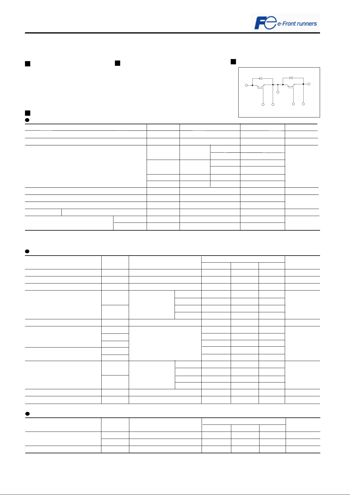
1200V / 300A 2 in one-package
Equivalent Circuit Schematic
C1
C2E1
G1 E1
G2 E2
Absolute maximum ratings (at Tc=25°C unless otherwise specified)
Item Symbol
Collector-Emitter voltage VCES
Gate-Emitter voltaga VGES
Collector current IC
ICp
-IC
-IC pulse
Collector Power Dissipation PC
Junction temperature Tj
Storage temperature Tstg
Isolation voltage between terminal and copper base *1 Viso
Screw Torque Mounting *2
Terminals *2
*1 : All terminals should be connected together when isolation test will be done.
*2 : Recommendable value : Mounting 2.5 to 3.5 N·m(M5 or M6), Terminals 3.5 to 4.5N·m(M6)
Conditions
Continuous
1ms
1 device
AC:1min.
Tc=25°C
Tc=80°C
Tc=25°C
Tc=80°C
Rating
1200
±20
400
300
800
600
300
600
1470
+150
-40 to +125
2500
3.5
4.5
Unit
V
V
A
W
°C
VAC
N·m
Electrical characteristics (at Tj=25°C unless otherwise specified)
Item
Symbols Conditions Characteristics Unit
Zero gate voltage collector current
Gate-Emitter leakage current
Gate-Emitter threshold voltage
Collector-Emitter saturation voltage
Input capacitance
Turn-on time
Turn-off time
Forward on voltage
Reverse recovery time
Lead resistance, terminal-chip*3
*3:Biggest internal terminal resistance among arm.
ICES
IGES
VGE(th)
VCE(sat)
(terminal)
VCE(sat)
(chip)
Cies
ton
tr
tr(i)
toff
tf
VF
(terminal)
VF
(chip)
trr
R lead
VGE=0V, VCE=1200V
VCE=0V, VGE=±20V
VCE=20V, IC=300mA
VGE=15V, IC=300A
VCE=10V, VGE=0V, f=1MHz
VCC=600V
IC=300A
VGE=±15V
RG=1.1 Ω
VGE=0V
IF=300A
IF=300A
Tj=25°C
Tj=125°C
Tj=25°C
Tj=125°C
Tj=25°C
Tj=125°C
Tj=25°C
Tj=125°C
Min. Typ. Max.
– – 2.0
– – 400
4.5 6.5 8.5
– 1.90 2.25
– 2.15 –
– 1.75 2.10
– 2.00 –
–34 –
– 0.36 1.20
– 0.21 0.60
– 0.03 –
– 0.37 1.00
– 0.07 0.30
– 1.75 2.05
– 1.85 –
– 1.60 1.90
– 1.70 –
– – 0.35
– 0.52 –
mA
nA
V
V
nF
µs
V
µs
mΩ
Thermal resistance characteristics
Items Symbols Conditions Characteristics Unit
Min. Typ. Max.
Thermal resistance
Contact Thermal resistance
*4 : This is the value which is defined mounting on the additional cooling fin with thermal compound.
Rth(j-c)
Rth(j-c)
Rth(c-f)*4
IGBT
FWD
With thermal compound
– – 0.085
– – 0.14
– 0.025 –
°C/W
°C/W
°C/W
E2
Page 2
2MBI300UD-120
Characteristics (Representative)
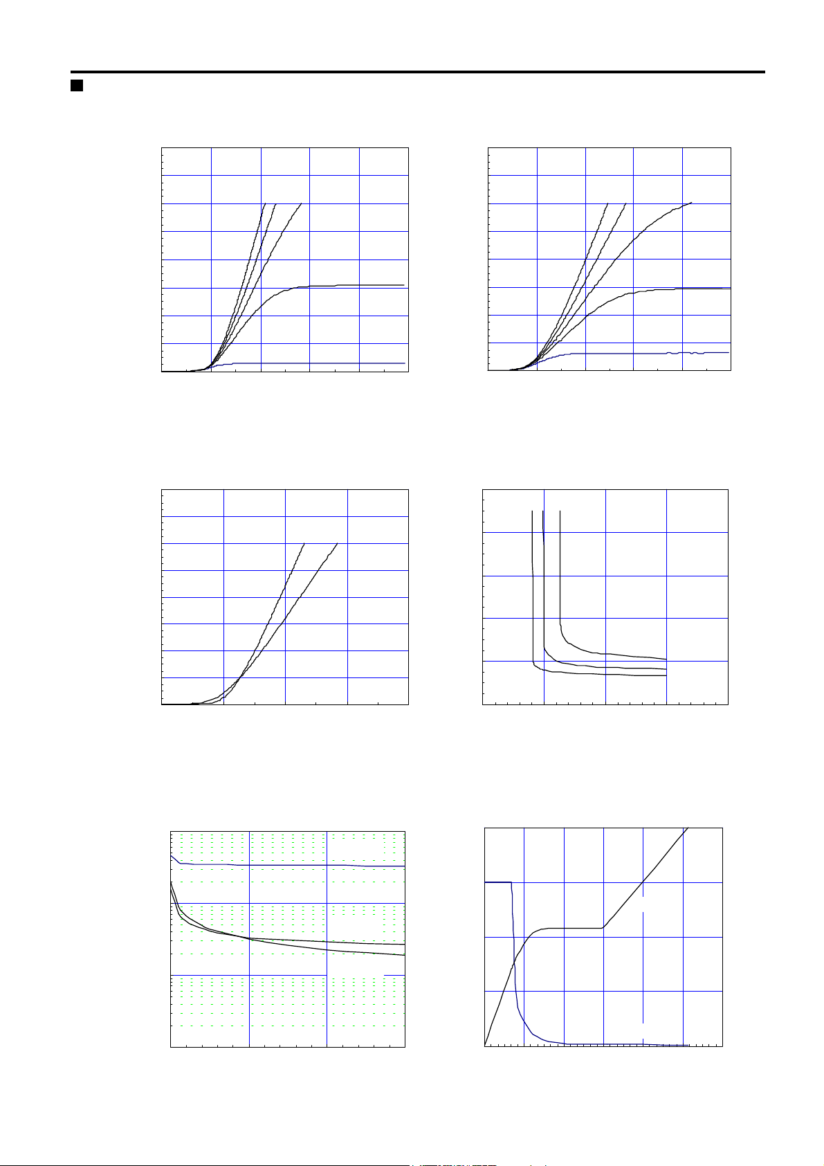
Collect or current vs. Collecto r-Emit ter voltage (ty p.)
Tj= 25°C / chip
800
IGBT Module
Collect or current vs. Collecto r-Emit ter voltage (ty p.)
Tj= 125°C / chip
800
700
600
500
400
300
Collector current : Ic [A]
200
100
0
012345
Collect or current vs. Collecto r-Emit ter voltage (ty p.)
800
700
600
500
400
300
Collector current : Ic [A]
200
100
0
01234
VGE=20V 15V 12V
Collector-Emit t er voltage : VCE [V]
VGE=15V / chip Tj=25°C / chip
Tj=125°CTj=25°C
10V
8V
700
600
500
400
300
Collector current : Ic [A]
200
100
0
012345
Collector-Emitter voltage : VCE [V]
VGE=20V 15V 12V
Collector-Emitter voltage vs. Gate-Emitter voltage (typ.)
10
8
6
4
2
Collector - Emitter voltage : VCE [ V ]
0
5 10152025
10V
8V
Ic=600A
Ic=300A
Ic=150A
Collector-Emit t er voltage : VCE [V]
Cap acit ance vs. Collect or-Emitter voltage (t y p .) Dy namic Gat e charge (ty p.)
VGE=0V, f= 1MHz, Tj= 25°C
100.0
10.0
1.0
Capacitance : Cies, Coes, Cres [ nF ]
0.1
0102030
Collector-Emit t er voltage : VCE [V]
Cies
Cres
Coe s
Gat e - E m it t er vo lt age : VGE [ V ]
Vcc=600V, Ic=300A, Tj= 25°C
Gate - Emitter voltage : VGE [ 5V/div ]
Collector-Emitter voltage : VCE [ 200V/div ]
0 300 600 900 1200 1500 1800
Gat e charge : Qg [ nC ]
VGE
VCE
Page 3

2MBI300UD-120
IGBT Module
Switching time vs. Collector current (typ.)
Vcc=600V, VGE=±15V, Rg=1.1Ω, Tj= 25°C
10000
1000
100
Switching time : ton, tr, toff, tf [ nsec ]
10
0 100 200 300 400 500 600
Collector current : Ic [ A ]
Switching time vs. Gate resistance (typ.)
Vcc=600V, Ic=300A, VGE=±15V, Tj= 25°C
10000
1000
tr
100
Switching time : ton, tr, toff, tf [ nsec ]
10
0.1 1.0 10.0 100.0
Gate resistance : Rg [ Ω ]
ton
toff
tr
tf
ton
toff
Switching time vs. Collector current (typ.)
Vcc=600V, VGE=±15V, Rg=1.1Ω, Tj=125°C
10000
1000
100
Switching time : ton, tr, toff, tf [ nsec ]
10
0 100 200 300 400 500 600
Collector current : Ic [ A ]
toff
ton
tr
tf
Switching loss vs. Collector current (typ.)
Vcc=600V, VGE=±15V, Rg=1.1Ω
60
50
40
30
20
tf
10
Switching loss : Eon, Eoff, Err [ mJ/pulse ]
0
0 100 200 300 400 500 600
Collector current : Ic [ A ]
Eoff(1 25°C)
Eon(125°C)
Eoff(2 5°C)
Eon(25°C)
Err(125°C)
Err(25°C)
Switching loss vs. Gate resistance (typ.)
Vcc=600V, Ic=300A, VGE=±15V, Tj= 125°C
250
200
150
100
50
Switching loss : Eon, Eoff, Err [ mJ/pulse ]
0
0.1 1.0 10.0 100.0
Gate resistance : Rg [ Ω ]
Eon
Eoff
Err
Reverse bias safe operating area (max.)
+VGE=15V,-VGE <= 15V, RG >= 1.1Ω ,Tj <=125°C
800
700
600
500
400
300
Collector current : Ic [ A ]
200
100
0
0 400 800 1200
Collector - Emitter voltage : VCE [ V ]
Page 4

2MBI300UD-120
IGBT Module
Forwar d current vs. F or war d on voltage (t yp.)
800
700
600
500
400
300
Forward current : IF [ A ]
200
100
0
01234
Forward on volt age : VF [ V ]
Transient t hermal resistance ( max . )
Tj=25°C
chip
Tj=125°C
Reverse recovery characteristics (typ.)
Vcc=6 00V, VG E=± 15V, Rg=1 .1Ω
1000
100
Reverse recovery current : Irr [ A ]
Reverse recovery time : trr [ nsec ]
10
0 100 200 300 400 500 600
Forward current : IF [ A ]
Irr (125°C)
Irr (25°C)
trr (125°C)
trr (25°C)
1.000
0.100
0.010
Thermal resistanse : Rth(j-c) [ °C/W ]
0.001
0.001 0.010 0.100 1.000
Pulse width : Pw [ sec ]
Outline Drawings, mm
M235
FWD
IGBT
 Loading...