Ftdi FT232RL, FT232RQ Schematics

FT232R USB UART IC Datasheet
Version 2.13
N eith er the whol e nor any part of the informat io n co ntained in, or the produ c t des c ribed in thi s manual, may be adapt ed or re produc ed
in a ny materia l or elec tro ni c form witho ut the pri or written c ons en t of the c opyrigh t ho ld er. This produc t and its doc u menta ti on are
s upplied on an as -i s bas is and no warra nt y as to thei r s ui ta bi lity for any parti c ul ar purp ose is either made or imp li ed . Future Te chnology
Dev ic es I nternat ional Ltd will not ac c e pt any c lai m for dama ge s hows oev er ari s ing as a re s ult of us e or fail ure of this prod u c t. Y o ur
s ta tu tory righ ts are not affec te d. Th is prod uct or any va riant of it is not intende d for us e in any medic al appl i anc e, dev ic e o r s ys te m in
whic h the failure of t he produc t might rea s o na bl y be e xp ec te d to res ul t in pe rs o nal injury . T hi s do c um ent pro vides p relimin ar y
info rma ti on tha t may be s ubje c t to change without notice. No free do m to use pate nts or other inte lle ctu a l property righ ts i s implie d by
the publi c a ti on of thi s doc u ment. F utu re T ec hno logy D evi c e s I nt ernationa l Lt d, Unit 1, 2 Seaward Place, Centurion Business Park, Glasgow
G41 1HH U ni te d K ingdom. S c otland Re gi s t ered C ompa ny N umber: SC 13 6 6 4 0
Future Technology Devices
International Ltd.
FT232R USB UART IC
The FT232R is a USB to serial UART
interface with the following advanced
features:
Single chip USB to as ynchronous serial da ta
transfer inte rface.
Entire USB protocol handled on the chip. No
USB spe cific firmware programming required.
Fully integrate d 1024 bit EEPROM storing
device descriptors and CBUS I/O configuration.
Fully integrated USB termination resistors.
Fully integrate d clock ge nera tion w ith no
external crysta l required plus optional clock
output selection enabling a glue-less interface
to exte rna l MCU or FPGA.
Data transfer rate s from 300 ba ud to 3 Mbaud
(RS422, RS485, RS232) at TTL levels.
128 byte rece ive buffer and 256 byte transmit
buffer utilising buffer smoothing te chnology to
allow for high data throughput.
FTDI’s royalty-free Virtua l Com Port (VCP) and
Direct (D2XX) drivers eliminate the
requirement for USB driver development in
most cases.
Unique USB FTDIChip-ID™ feature.
Configurable CBUS I/O pins.
Transmit and receive LED drive signa ls.
UART interface supp ort for 7 or 8 data bits, 1
or 2 stop bits and odd / even / mark / space /
no parity
FIFO receives a nd transmits buffers for high
data throughput.
Synchronous and asynchronous bit bang
interface options with RD# and WR# strobe s .
Device supplied pre -programmed w ith unique
USB serial numbe r.
Supports bus powered, self-powered and high-
power bus po w e red USB configurations.
Integrated +3.3V level converter for USB I/O.
Integrated level converter on UART and CBUS
for interfacing to betw e e n +1.8V and +5V
logic.
True 5V/3.3V/2.8V/1.8V CMOS drive output
and TTL input.
Configurable I/O pin output drive strength.
Integrated pow er-on-rese t circuit.
Fully inte grated AVCC supply filtering - no
external filtering required.
UART signal inversion option.
+3.3V (using e xte rnal oscillator) to +5.25V
(internal oscillator) Single Supply Operation.
Low operating and USB suspe nd current.
Low USB bandw idth consumption.
UHCI/OHCI/EHCI hos t controller compatible .
USB 2.0 Full Spe ed compatible.
-40°C to 85°C extended operating temperature
range.
Available in compa ct Pb-free 28 Pin SSOP and
QFN-32 packages (both RoHS compliant).
Copyright © 2015 Future Technology Devices International Limited 1

FT232R USB UART IC Datasheet
Version 2.13
USB to RS232/RS422/RS485 Converters
Upgrading Legacy Peripherals to USB
Cellular and Cordless Phone USB data transfer
cables and interfaces
Interfacing MCU/PLD/FPGA based designs to
USB
USB Audio and Low Bandwidth Video data
transfer
PDA to USB data transfer
USB Smart Card Readers
USB Instrumentation
USB Indus trial Control
USB MP3 Player Inte rface
USB FLASH Ca rd Reader and Writers
Set Top Box PC - USB interface
USB Digital Camera Interface
USB Hardw are Modems
USB Wireless Modems
USB Bar Code Readers
USB Software and Hardware Encryption
Dongles
Royalty free VIRTUAL COM PORT
(VCP) DRIVERS for...
Windo ws 10 32,64-bit
Windo ws 8/8.1 32,64-bit
Windo ws 7 32,64-bit
Windo ws Vista and Vista 64-bit
Windo ws XP and XP 64-bit
Windo ws 98, 98SE, ME, 2000, Server 2003, XP,
Server 2008 and server 2012 R2
Windo ws XP Embedded
Windo ws CE 4.2, 5.0 and 6.0
Mac OS 8/9, OS-X
Linux 2.4 and greater
Royalty free D2XX Direct Drivers
(USB Drivers + DLL S/W Interface)
Windows 10 32,64-bit
Windows 8/8.1 32,64-bit
Windows 7 32,64-bit
Windows Vista and Vista 64-bit
Windows XP and XP 64-bit
Windows 98, 98SE, ME, 2000, Server 2003, XP,
Server 2008 and server 2012 R2
Windows XP Embedded
Windows CE 4.2, 5.0 and 6.0
Linux 2.4 and greater
Android(J2xx)
1 Typical Applications
1.1 Driver Support
The drivers listed abo ve are all available to download for free from FTDI we bsite (ww w .ftdichip.com).
Various 3rd party drivers a re a lso ava ilable for other operating systems - see FTDI w e bsite
(ww w.ftdichip.com) for details.
For driver installation, please refer to http://ww w .ftdichip.com/Documents/InstallGuide s.htm
Copyright © 2015 Future Technology Devices International Limited 2
FT232R USB UART IC Datasheet
Version 2.13
Part Number
Package
FT232RQ-xxxx
32 Pin QFN
FT232RL-xxxx
28 Pin SSOP
1.2 Part Numbers
Note: Packing codes for xxxx is:
- Ree l: Tape d and Ree l, (SSOP is 2,000pcs pe r reel, QFN is 6,000pcs per reel).
- Tube : Tube pa cking, 47pcs per tube (SSOP only)
- Tray: Tray packing, 490pcs per tray (QFN only)
For example: FT232RQ-Reel is 6,000pcs taped and reel packing
1.3 USB Compliant
The FT232R is fully compliant with the USB 2.0 specification and has been given the USB-IF Test-ID (TID)
40680004 (Rev B) and 40770018 (Rev C).
Copyright © 2015 Future Technology Devices International Limited 3
FT232R USB UART IC Datasheet
Version 2.13
x4 Clock
Multiplier
UART
FIFO Controller
Serial Interface
Engine
( SIE )
USB
Protocol Engine
Baud Rate
Generator
UART Controller
with
Programmable
Signal Inversion
3.3 Volt
LDO
Regulator
USB
Transceiver
with
Integrated
Series
Resistors
and 1.5K
Pull-
up
USB DPLL
Internal
12MHz
Oscillator
48MHz
48MHz
OCSI
(optional)
OSCO
(optional)
USBDP
USBDM
3V3OUT
VCC
DBUS0
DBUS1
DBUS2
DBUS3
DBUS4
DBUS5
DBUS6
DBUS7
CBUS0
CBUS2
CBUS3
SLEEP#
RESET#
TEST
GND
Reset
Generator
3V3OUT
CBUS1
FIFO RX
Buffer
FIFO TX Buffer
Internal
EEPROM
To USB Transeiver Cell
CBUS4
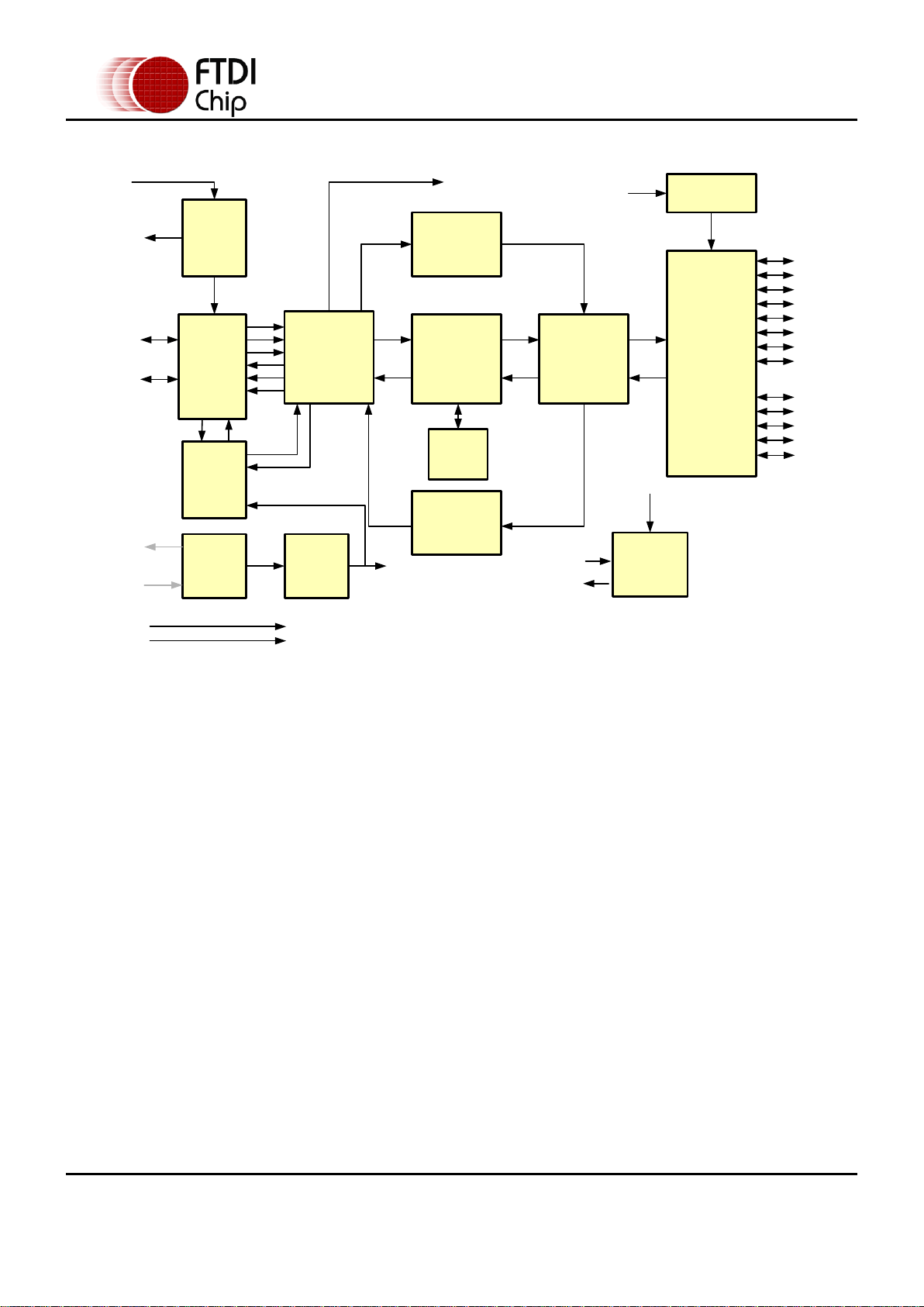
2 FT232R Block Diagram
Figure 2.1 FT232R Block Diagram
For a description of each function please refer to Section 4.
Copyright © 2015 Future Technology Devices International Limited 4

FT232R USB UART IC Datasheet
Version 2.13
Table of Contents
1 Typical Applications .................................................... 2
1.1 Driver Support ........................................................................ 2
1.2 Part Numbers ......................................................................... 3
1.3 USB Compliant ........................................................................ 3
2 FT232R Block Diagram ................................................ 4
3 Device Pin Out and Signal Description .......................... 7
3.1 28-LD SSOP Package ............................................................... 7
3.2 SSOP Package Pin Out Description........................................... 7
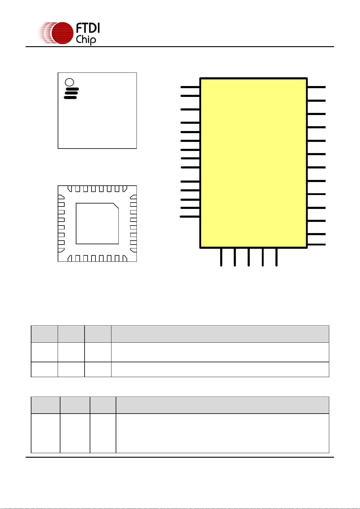
3.3 QFN-32 Package ....................................................................10
3.4 QFN-32 Package Signal Description ........................................10
3.5 CBUS Signal Options ..............................................................13
4 Function Description ................................................. 14
4.1 Key Features..........................................................................14
4.2 Functional Block Descriptions .................................................15
5 Devices Characteristics and Ratings ........................... 17
5.1 Absolute Maximum Ratings ....................................................17
5.2 DC Characteristics..................................................................18
5.3 EEPROM Reliability Characteristics .........................................21
5.4 Internal Clock Characteristics.................................................21
5.5 Thermal Characteristics .........................................................22
6 USB Power Configurations ......................................... 23
6.1 USB Bus Powered Configuration ............................................23
6.2 Self Powered Configuration ....................................................24
6.3 USB Bus Powered with Power Switching Configuration............25
6.4 USB Bus Powered with Selectable External Logic Supply .........26
7 Application Examples ................................................ 28
7.1 USB to RS232 Converter .........................................................28
7.2 USB to RS485 Converter .........................................................29
7.3 USB to RS422 Converter .........................................................30
7.4 USB to MCU UART Interface....................................................31
Copyright © 2015 Future Technology Devices International Limited 5

FT232R USB UART IC Datasheet
Version 2.13
7.5 LED Interface.........................................................................32
7.6 Using the External Oscillator ..................................................33
8 Internal EEPROM Configuration ................................. 34
9 Package Parameters .................................................. 36
9.1 SSOP-28 Package Dimensions ................................................36
9.2 QFN-32 Package Dimensions ..................................................37
9.3 QFN-32 Package Typical Pad Layout .......................................38
9.4 QFN-32 Package Typical Solder Paste Diagram .......................39
9.5 Solder Reflow Profile .............................................................39
10 Alternative Parts ....................................................... 41
11 Contact Information .................................................. 42
Appendix A – References ................................................. 43
Document References ....................................................................43
Acronyms and Abbreviations ..........................................................43
Appendix B – List of Figures and Tables............................ 44
List of Figures................................................................................44
List of Tables .................................................................................44
Appendix C – Revision History.......................................... 46
Copyright © 2015 Future Technology Devices International Limited 6
FT232R USB UART IC Datasheet
Version 2.13
Pin No.
Name
Type
Description
15
USBDP
I/O
USB Data Signal Plus, incorporating internal series resistor and 1.5kΩ pull up
resistor to 3.3V.
16
USBDM
I/O
USB Data Signal Minus, incorporating internal series resistor.
Pin No.
Name
Type
Description
4
VCCIO
PW R
+1.8V to +5.25V supply to the UART Interface and CBUS group pins (1...3, 5, 6,
9...14, 22, 23). In USB bus powered designs connect this pin to 3V3OUT pin to
drive out at +3.3V levels, or connect to VCC to drive out at 5V CMOS level. This
pin can also be supplied with an external +1.8V to +2.8V supply in order to drive
outputs at lower levels. It should be noted that in this case this supply should
originate from the same source as the supply to VCC. This means that in bus
powered designs a regulator which is supplied by the +5V on the USB bus should
USBDP
USBDM
3V3OUT
GND
RESET#
VCC
GND
NC
AGND
TEST
OSCI
OSCO
CBUS1
CBUS0
TXD
RTS#
RXD
DTR#
VCCIO
RI#
GND
NC
DSR#
DCD#
CTS#
CBUS4
CBUS2
CBUS3
1
14
15
28
FT232RL
A
G
N
D
G
N
D
G
N
D
G
N
D
T
E
S
T
25 7 18 21 26
3V3OUT
VCCIO
4
17
NC
RESET#
NC
24
19
8
TXD
RXD
RTS#
CTS#
DTR#
DSR#
DCD#
RI#
1
5
3
11
2
9
10
6
CBUS0
CBUS3
CBUS2
CBUS1
23
22
13
14
20
16
15
USBDP
USBDM
VCC
OSCI
27
OSCO
28
CBUS4
12
FTDI
FT232RL
YYXX-A
XXXXXXXXXXXX
3 Device Pin Out and Signal Description
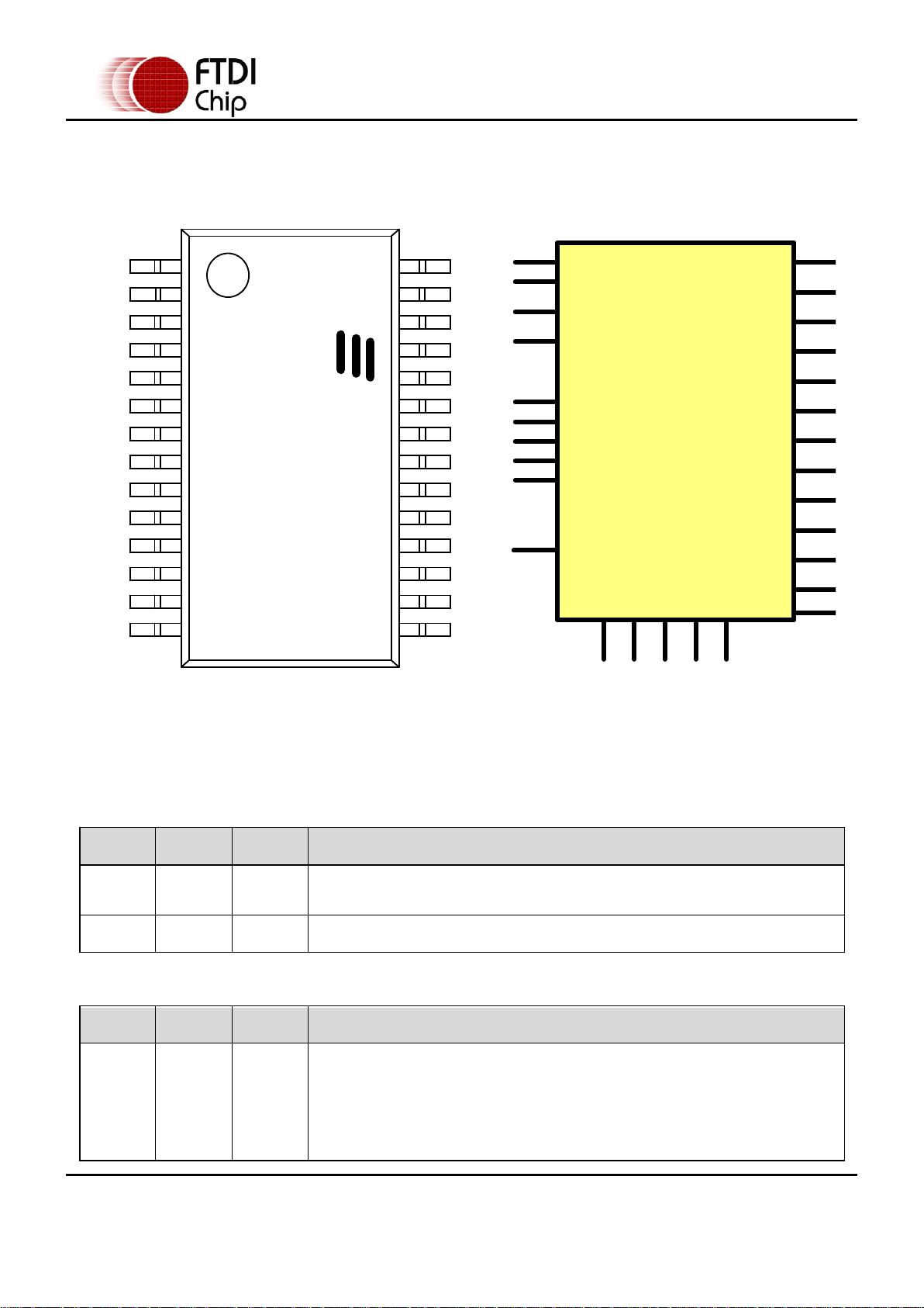
3.1 28-LD SSOP Package
Figure 3.1 SSO P Package Pin Out and Schematic Symbol
3.2 SSOP Package Pin Out Description
Note: The conve ntion used throughout this document for active low signals is the signal name follow e d
by#
Copyright © 2015 Future Technology Devices International Limited 7
Table 3.1 USB Interface Group
FT232R USB UART IC Datasheet
Version 2.13
Pin No.
Name
Type
Description
be used.
7, 18,
21
GND
PW R
Device ground supply pins
17
3V3OUT
Output
+3.3V output from integrated LDO regulator. This pin should be decoupled to
ground using a 100nF capacitor. The main use of this pin is to provide the internal
+3.3V supply to the USB transceiver cell and the internal 1.5kΩ pull up resistor on
USBD P. Up to 50mA can be drawn from this pin to power external logic if
required. This pin can also be used to supply the VCCIO pin.
20
VCC
PW R
+3.3V to +5.25V supply to the device core. (see Note 1)
25
AGND
PW R
Device analogue ground supply for internal clock multiplier
Pin No.
Name
Type
Description
8, 24
NC
NC
No internal conne ction
19
RESET#
Input
Active low rese t pin. This can be used by an exte rnal device to reset the
FT232R. If not required can be left unconnected, or pulled up to VCC.
26
TEST
Input
Puts the device into IC test mode . Must be tied to GND for normal
operation, othe rwise the device will appear to fail.
27
OSCI
Input
Input 12MHz Oscillator Cell. Optional – Can be left unconnected for
normal ope ration. (see Note 2)
28
OSCO
Output
Output from 12MHZ Oscillator Cell. Optional – Ca n be left unconnected
for normal opera tion if internal Oscillato r is used. (see Note 2)
Pin No.
Name
Type
Description
1
TXD
Output
Transmit Asynchronous Data Output.
2
DTR#
Output
Data Terminal Ready Control Output / Handshake Signal.
3
RTS#
Output
Request to Send Control Output / Handshake Signal.
5
RXD
Input
Receiving Asynchronous Data Input.
6
RI#
Input
Ring Indicator Control Input. When remote wake up is enabled in the
internal EEPROM taking RI# low (20ms active low pulse) can be used to
resume the PC USB host controller from s uspend.
9
DSR#
Input
Data Set Ready Control Input / Handshake Signal.
10
DCD#
Input
Data Carrier Dete ct Control Input.
Table 3.2 Power and Ground Group
Table 3.3 Miscellaneous Signal Group
Copyright © 2015 Future Technology Devices International Limited 8

FT232R USB UART IC Datasheet
Version 2.13
Pin No.
Name
Type
Description
11
CTS#
Input
Clear To Send Control Input / Handsha ke Signal.
12
CBUS4
I/O
Configurable CBUS output only Pin. Function of this pin is configured in
the device internal EEPROM. Factory default configuration is SLEEP#. See
CBUS Signal Options, Table 3.99.
13
CBUS2
I/O
Configurable CBUS I/O Pin. Function of this pin is configured in the
device inte rnal EEPROM. Factory default configura tion is TXDEN. See
CBUS Signal Options, Table 3.99.
14
CBUS3
I/O
Configurable CBUS I/O Pin. Function of this pin is configured in the
device inte rnal EEPROM. Factory default configura tion is PW REN#. Se e
CBUS Signal Options, Table 3.99. PW REN# should be used with a 10kΩ
resistor pull up.
22
CBUS1
I/O
Configurable CBUS I/O Pin. Function of this pin is configured in the
device inte rnal EEPROM. Factory default configuration is RXLED#. See
CBUS Signal Options, Table 3.99.
23
CBUS0
I/O
Configurable CBUS I/O Pin. Function of this pin is configured in the
device inte rnal EEPROM. Factory default configura tion is TXLED#. See
CBUS Signal Options, Table 3.99.
Table 3.4 UART Interface and CUSB Group (see note 3)
Notes :
1. The minimum operating voltage VCC must be +4.0V (could use VBUS=+5V) w hen using the
internal clock generator. Opera tion at +3.3V is pos sible using an external crystal oscillator.
2. For details on how to use an externa l crystal, ceramic resona to r, or oscillator with the FT232R,
pleas e refer Section 7.6
3. Whe n used in Input Mode, the input pins are pulled to VCCIO via interna l 200kΩ resistors. These
pins can be programmed to gently pull low during USB suspend (PW REN# = “1”) by setting an
option in the inte rna l EEP ROM.
Copyright © 2015 Future Technology Devices International Limited 9
FT232R USB UART IC Datasheet
Version 2.13
Pin No.
Name
Type
Description
14
USBDP
I/O
USB Data Signal Plus, incorporating internal series resistor and 1.5kΩ pull up resistor
to +3.3V.
15
USBDM
I/O
USB Data Signal Minus, incorporating internal series resistor.
Pin No.
Name
Type
Description
1
VCCIO
PW R
+1.8V to +5.25V supply for the UART Interface and CBUS group pins (2,3,
6,7,8,9,10,11,21,22,30,31,32). In USB bus powered designs connect this pin to
3V3OUT to drive out at +3.3V levels, or connect to VCC to drive out at +5V CMOS
level. This pin can also be supplied with an external +1.8V to +2.8V supply in order
to drive out at lower levels. It should be noted that in this case this supply should
originate from the same source as the supply to VCC. This means that in bus
FT232RQ
32
25
24
17
169
8
1
YYXX-A
18
9
1
2
3
4
5
6
7
8
10111213141516
17
19
20
21
22
23
24
25 26 27 28 29 30 31 32
USBDP
USBDM
3V3OUT
RESET#
VCC
NC
AGND
TEST
OSCI
OSCO
CBUS1
CBUS0
TXD
RTS#
RXD
DTR#
VCCIO
RI#
GND
NC
DSR#
DCD#
CTS#
CBUS4
CBUS2
CBUS3
GND
GND
NC
NC
NC
NC
I
FT232RQ
A
G
N
D
G
N
D
G
N
D
G
N
D
T
E
S
T
24 4 17 20 26
3V3OUT
VCCIO
1
16
NC
RESET#
NC
23
18
13
TXD
RXD
RTS#
CTS#
DTR#
DSR#
DCD#
RI#
30
2
32
8
31
6
7
3
CBUS0
CBUS3
CBUS2
CBUS1
22
21
10
11
19
15
14
USBDP
USBDM
VCC
OSCI
27
OSCO
28
CBUS4
9
NC
12
NC
5
NC
29
NC
25
FTD
XXXXXXX
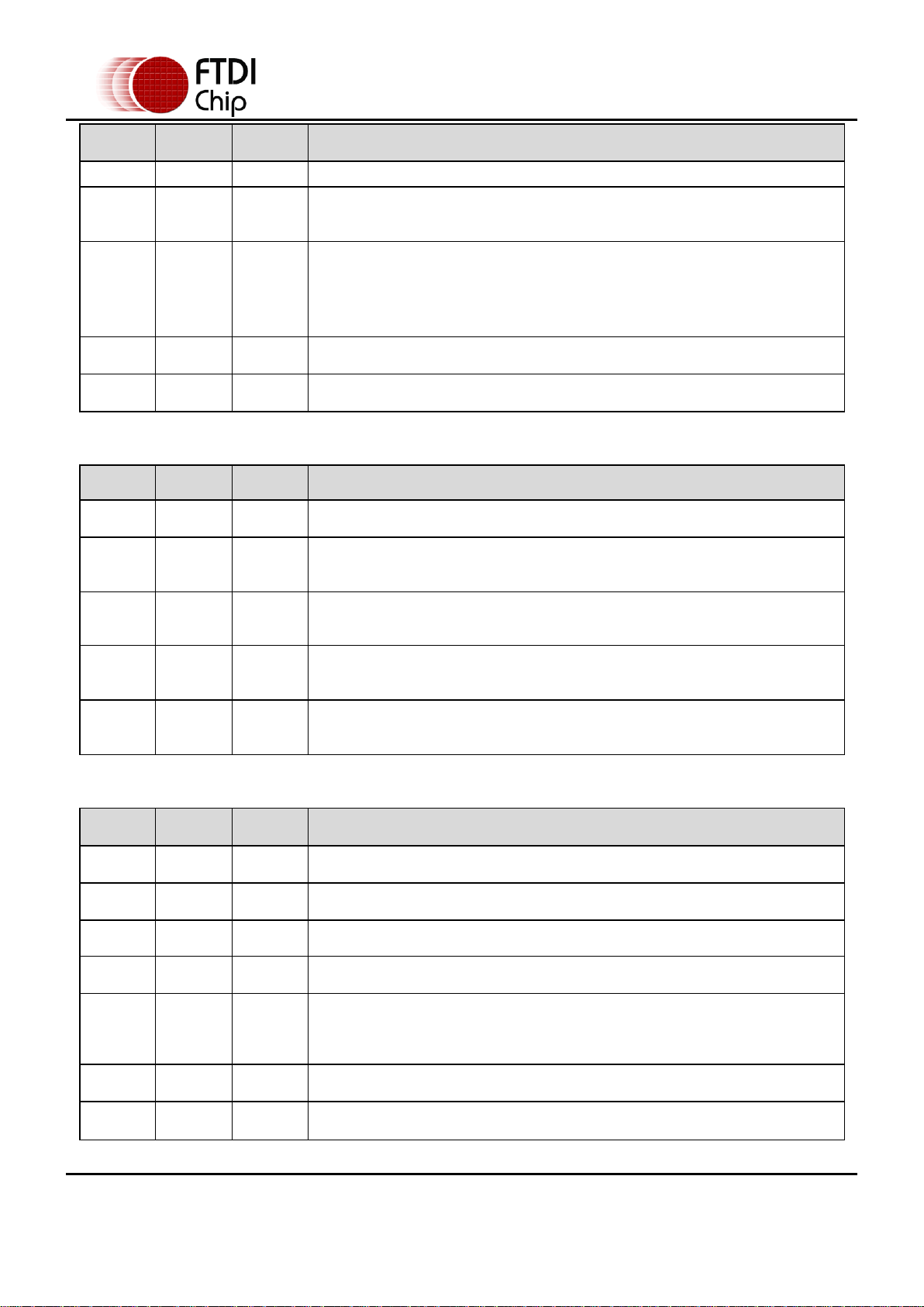
3.3 QFN-32 Package
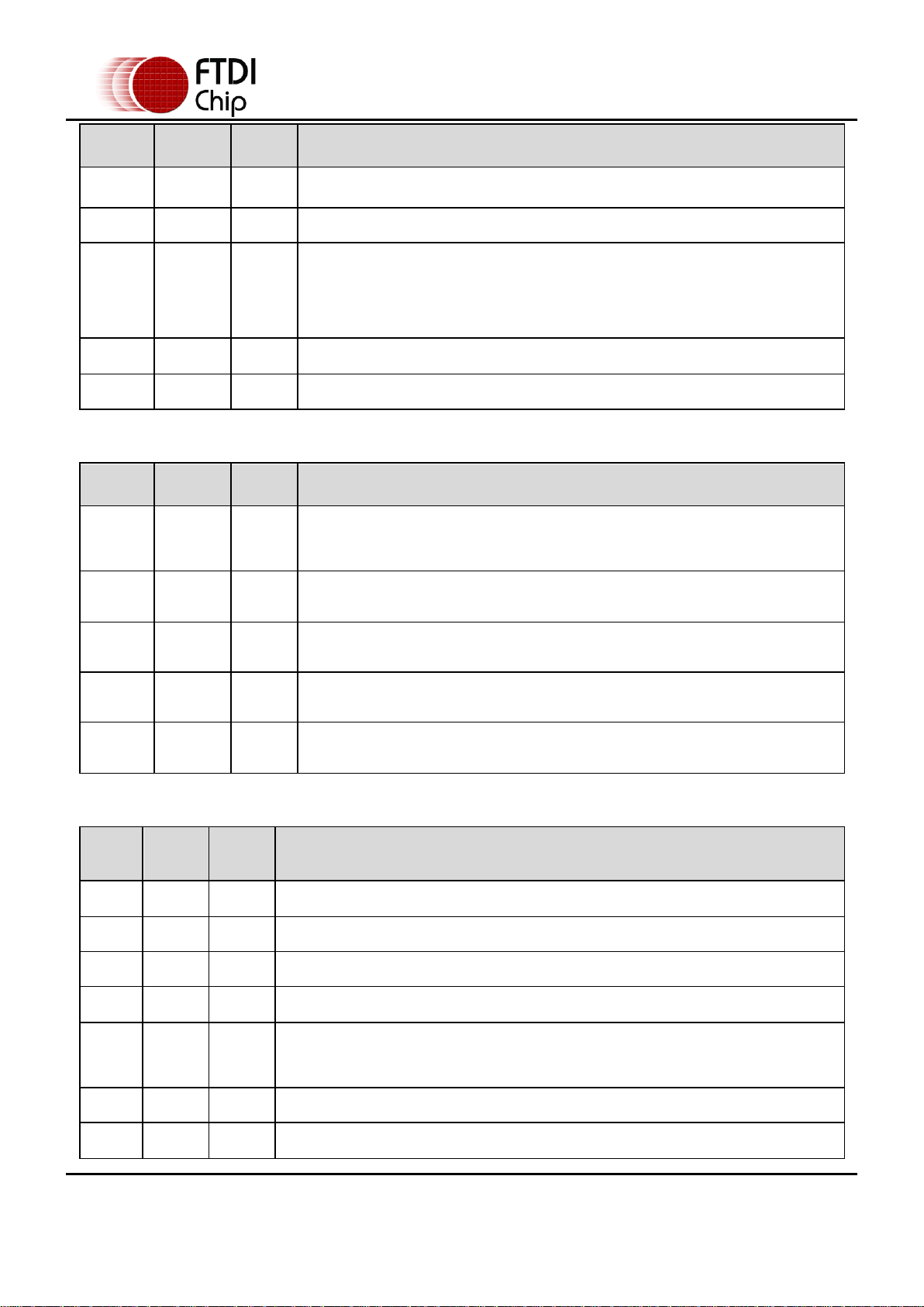
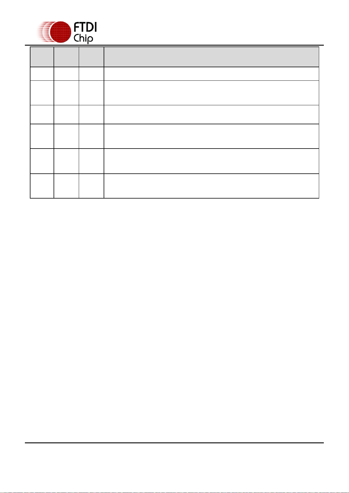
3.4 QFN-32 Package Signal Description
Copyright © 2015 Future Technology Devices International Limited 10
Figure 3.2 Q FN-32 Package Pin Out and schematic symbol
Table 3.5 USB Interfac e Group
FT232R USB UART IC Datasheet
Version 2.13
Pin No.
Name
Type
Description
powered designs a regulator which is supplied by the +5V on the USB bus should be
used.
4, 17, 20
GND
PWR
Device ground supply pins.
16
3V3OUT
Output
+3.3V output from integrated LDO regulator. This pin should be decoupled to
ground using a 100nF capacitor. The purpose of this output is to provide the
internal +3.3V supply to the USB transceiver cell and the internal 1.5kΩ pull up
resistor on USBDP. Up to 50mA can be drawn from this pin to power external logic if
required. This pin can also be used to supply the VCCIO pin.
19
VC C
PWR
+3.3V to +5.25V supply to the device core. (See Note 1).
24
AGND
PWR
Device analogue ground supply for internal clock multiplier.
Pin No.
Name
Type
Description
5, 12,
13, 23,
25, 29
NC
NC
No internal connection. Do not connect.
18
RESET#
Input
Active low reset. Can be used by an external device to reset the FT232R. If not
required can be left unconnected, or pulled up to VCC.
26
TEST
Input
Puts the device into IC test mode. Must be tied to GND for normal operation,
otherwise the device will appear to fail.
27
OSC I
Input
Input 12MHz Oscillator Cell. Optional – Can be left unconnected for normal
operation. (See Note 2).
28
OSC O
Output
Output from 12MHZ Oscillator Cell. Optional – Can be left unconnected for normal
operation if internal Oscillator is used. (See Note 2).
Pin
No.
Name
Type
Description
30
TXD
Output
Transmit Asynchronous Data Output.
31
DTR#
Output
Data Terminal Ready Control Output / Handshake Signal.
32
RTS#
Output
Request to Send Control Output / Handshake Signal.
2
RXD
Input
Receiving Asynchronous Data Input.
3
RI#
Input
Ring Indicator Control Input. When remote wake up is enabled in the internal EEPROM
taking RI# low (20ms active low pulse) can be used to resume the PC USB host
controller from suspend.
6
DSR#
Input
Data Set Ready Control Input / Handshake Signal.
7
DC D#
Input
Data C arrier Detect Control Input.
Table 3.6 Power and Ground Group
Table 3.7 Miscellaneous Signal Group
Copyright © 2015 Future Technology Devices International Limited 11
FT232R USB UART IC Datasheet
Version 2.13
Pin
No.
Name
Type
Description
8
CTS#
Input
Clear To Send Control Input / Handshake Signal.
9
CBUS4
I/O
Configurable CBUS output only Pin. Function of this pin is configured in the device
internal EEPROM. Factory default configuration is SLEEP#. See CBUS Signal Options,
Table 3.99.
10
CBUS2
I/O
Configurable CBUS I/O Pin. Function of this pin is configured in the device internal
EEPROM. Factory default configuration is TXDEN. See CBUS Signal Options, Table 3.99.
11
CBUS3
I/O
Configurable CBUS I/O Pin. Function of this pin is configured in the device internal
EEPROM. Factory default configuration is PWREN#. See CBUS Signal Options, Table
3.99. PWREN# should be used with a 10kΩ resistor pull up.
21
CBUS1
I/O
Configurable CBUS I/O Pin. Function of this pin is configured in the device internal
EEPROM. Factory default configuration is RXLED#. See CBUS Signal Options, Table
3.99.
22
CBUS0
I/O
Configurable CBUS I/O Pin. Function of this pin is configured in the device internal
EEPROM. Factory default configuration is TXLED#. See CBUS Signal Options, Table
3.99.
Table 3.8 UART Interface and CBUS Group (see note 3)
Notes :
1. The minimum operating voltage VCC must be +4.0V (could use VBUS=+5V) whe n using the
internal clock generator. Opera tion at +3.3V is pos sible using an external crystal oscillator.
2. For details on how to use an exte rna l crystal, ceramic reso nator, or oscillator with the FT232R,
pleas e refer to Section 7.6.
3. Whe n used in Input Mode, the input pins are pulled to VCCIO via internal 200kΩ resistors. These
pins can be programmed to gently pull low during USB suspend (PW REN# = “1”) by setting an
option in the inte rna l EEP ROM.
Copyright © 2015 Future Technology Devices International Limited 12

FT232R USB UART IC Datasheet
Version 2.13
CBUS
Signal
Option
Available On CBUS Pin
Description
TXDEN
CBUS0, C BUS1, C BUS2, CBUS3, C BUS4
Enable transmit data for RS485
PWREN#
CBUS0, C BUS1, C BUS2, CBUS3, C BUS4
Output is low after the device has been configured by
USB, then high during USB suspending mode. This output
can be used to control power to external logic P-Channel
logic level MOSFET switch. Enable the interface pull-down
option when using the PWREN# in this way.*
TXLED#
CBUS0, C BUS1, C BUS2, CBUS3, C BUS4
Transmit data LED drive: Data from USB Host to
FT232R. Pulses low when transmitting data via USB. See
Section 7.5 for more details.
RXLED#
CBUS0, C BUS1, C BUS2, CBUS3, C BUS4
Receive data LED drive: Data from FT232R to USB Host.
Pulses low when receiving data via USB. See Section 7.5
for more details.
TX&RXLED#
CBUS0, C BUS1, C BUS2, CBUS3, C BUS4
LED drive – pulses low when transmitting or receiving data
via USB. See Section 7.5 for more details.
SLEEP#
CBUS0, C BUS1, C BUS2, CBUS3, C BUS4
Goes low during USB suspend mode. Typically used to
power down an external TTL to RS232 level converter IC
in USB to RS232 converter designs.
CLK48
CBUS0, C BUS1, C BUS2, CBUS3, C BUS4
48MHz ±0.7% C lock output. **
CLK24
CBUS0, C BUS1, C BUS2, CBUS3, C BUS4
24 MHz Clock output.**
CLK12
CBUS0, C BUS1, C BUS2, CBUS3, C BUS4
12 MHz Clock output.**
CLK6
CBUS0, C BUS1, C BUS2, CBUS3, C BUS4
6 MHz ±0.7% Clock output. **
CBitBangI/O
CBUS0, C BUS1, C BUS2, CBUS3
CBUS bit bang mode option. Allows up to 4 of the CBUS
pins to be used as general purpose I/O. Configured
individually for CBUS0, C BUS1, CBUS2 and CBUS3 in the
internal EEPROM. A separate application note, AN232R-01,
available from FTDI website (www.ftdichip.com) describes
in more detail how to use CBUS bit bang mode.
BitBangWRn
CBUS0, C BUS1, C BUS2, CBUS3
Synchronous and asynchronous bit bang mode WR#
strobe output.
BitBangRDn
CBUS0, C BUS1, C BUS2, CBUS3
Synchronous and asynchronous bit bang mode RD# strobe
output.
3.5 CBUS Signal Options
The following options can be configured on the CBUS I/O pins. CBUS signa l options are common to both
package ve rsions of the FT232R. These options can be configured in the inte rnal EEP ROM using the
softw are utility FT_PPROG or MPROG, w hich can be dow nloa ded from the FTDI Utilities
(ww w.ftdichip.com). The default configuration is described in Section 8.
Table 3.9 CBUS Configuration Control
* PW REN# must be used with a 10kΩ res istor pull up.
**W hen in USB sus pend mode the outputs clocks are also suspende d.
Copyright © 2015 Future Technology Devices International Limited 13

FT232R USB UART IC Datasheet
Version 2.13
4 Function Description
The FT232R is a USB to se rial UART inte rface device which simplifies USB to serial de signs and reduces
external compone nt count by fully integrating an external EEPROM, USB termination res istors and an
integrate d clock circuit w hich requires no external crysta l, into the device. It ha s been des igned to
operate e fficiently with a USB host controller by using as little as possible of the to ta l USB bandw idth
available.
4.1 Key Features
Functional Integration. Fully integrate d EEPROM, USB termination res istors, clock generation, AVCC
filtering, POR and LDO regulator.
Configurable CBUS I/O Pin Options. The fully integrated EEPROM allows configuration of the Control
Bus (CBUS) functionality, signal inve rsion a nd drive strength se lection. There are 5 configurable CBUS
I/O pins. These configurable options are
1. TXDEN - transmit enable for RS485 des igns.
2. PWREN# - Pow er control for high pow er, bus pow ered designs.
3. TXLED# - for pulsing an LED upon transmission of data.
4. RXLED# - for pulsing an LED upon receiving data .
5. TX&RXLED# - which will pulse an LED upon tra nsmission OR reception of data .
6. SLEEP# - indicates that the de vice going into USB suspend mode.
7. CLK48 / CLK24 / CLK12 / CLK6 - 48MHz, 24MHz, 12MHz, and 6MHz clock output signa l
options.
The CBUS pins can also be individually configured as GPIO pins, similar to as ynchronous bit bang mode.
It is possible to use this mode while the UART interface is being used, thus providing up to 4 gene ral
purpose I/O pins which are available during normal operation. An application note, AN232R-01, available
from FTDI we bsite (ww w .ftdichip.com) describes this fea ture.
The CBUS lines can be configured with any one of thes e output options by setting bits in the inte rna l
EEP ROM. The device is supplied with the mos t commonly used pin definitions pre -programmed - se e
Section 8 for details.
Asynchronous Bit Bang Mode with RD# and WR# Strobes. The FT232R supports FTDI’s previous
chip ge neration bit-bang mode. In bit-bang mode, the eight UART lines can be sw itched from the regular
interface mode to an 8-bit general purpose I/O port. Data packets can be sent to the device and they w ill
be sequentially sent to the interface at a rate controlled by an internal timer (equivalent to the baud rate
pre-scaler). With the FT232R device this mode has bee n enhanced by outputting the inte rna l RD# and
WR# strobes signals which can be used to allow external logic to be clocked by accesses to the bit-bang
I/O bus . This option w ill be describe d more fully in a separate a pplication note available from FTDI
website (ww w.ftdichip.com).
Synchronous Bit Bang Mode. The FT232R supports synchronous bit bang mode. This mode differs from
as ynchronous bit bang mode in that the interface pins are only read when the device is written to. This
makes it eas ier for the controlling program to measure the respons e to an output stimulus as the data
returne d is synchronous to the output data. An application note, AN232R-01, available from FTDI w e bsite
(ww w.ftdichip.com) de scribes this feature.
FTDIChip-ID™. The FT232R a lso includes the new FTDIChip-ID™ se curity dongle feature. This
FTDIChip-ID™ feature allow s a unique number to be burnt into e a ch device during manufacture . This
numbe r cannot be reprogrammed. This number is only rea dable over USB and forms a basis of a se curity
dongle w hich can be use d to protect any customer application softw are being copied. This allows the
possibility of us ing the FT232R in a dongle for software licensing. Further to this, a renew able license
sche me can be implemented based on the FTDIChip -ID™ number when encrypted with other information.
This encrypte d numbe r can be stored in the user a rea of the FT232R internal EEPROM, a nd can be
decrypte d, then compared with the protected FTDIChip -ID™ to verify that a license is valid. We b based
applications can be used to mainta in product licensing this way. An application note, AN232R-02,
available from FTDI webs ite (www .ftdichip.com) describe s this feature.
The FT232R is capa ble of operating at a voltage supply betw e en +3.3V and +5V with a nominal
operational mode current of 15mA and a nominal USB suspend mode current of 70µA. This allow s greater
Copyright © 2015 Future Technology Devices International Limited 14

FT232R USB UART IC Datasheet
Version 2.13
margin for peripheral designs to mee t the USB suspend mode current limit of 2.5mA. An integrated level
conve rte r within the UART interface allow s the FT232R to interface to UART logic running at +1.8V, 2.5V,
+3.3V or +5V.
4.2 Functional Block Descriptions
The following paragraphs detail e ach function within the FT232R. Please refer to the block diagram shown
in Figure 2.1
Internal EEPROM. The internal EEP ROM in the FT232R is used to store USB Vendor ID (VID), Product ID
(PID), device serial number, product des cription string and various other USB configuration de scriptors .
The internal EEPROM is also used to configure the CBUS pin functions . The FT232R is supplied with the
internal EEPROM pre -pro grammed as described in Se ction 8. A use r area of the internal EEPROM is
available to system designers to allow storing additional data. The internal EEPROM descriptors can be
programmed in circuit, over USB w ithout any additional volta ge re quirement. It can be programmed
using the FTDI utility softw are called MPROG, which can be downloaded from FTDI Utilities on the FTDI
website (ww w.ftdichip.com).
+3.3V LDO Regulator. The +3.3V LDO regulator generates the +3.3V reference voltage for driving the
USB tra ns ceiver cell output buffers. It requires an external decoupling capacitor to be atta che d to the
3V3OUT regulator output pin. It a ls o provides +3.3V power to the 1.5kΩ internal pull up resisto r on
USBDP. The main function of the LDO is to pow e r the USB Trans ceiver and the Reset Generator Cells
rather than to po w e r external logic. However, it can be used to supply external circuitry re quiring a
+3.3V nominal supply with a maximum current of 50mA.
USB Transceiver. The USB Transceiver Cell provide s the USB 1.1 / USB 2.0 full-spee d physical inte rface
to the USB cable. The output drivers provide +3.3V level slew rate control signalling, whi lst a differential
input receiver and tw o single ended input receivers provide USB data in, Single -Ended-0 (SE0) and USB
reset detection conditions respectfully. This function also incorpo rates the internal USB series termination
resistors on the USB data lines and a 1.5kΩ pull up resistor on USBDP.
USB DPLL. The USB DPLL cell locks on to the incoming NRZI USB data and ge nera te s recovered clock
and data signals for the Serial Interface Engine (SIE) block.
Internal 12MHz Oscillator - The Internal 12MHz Oscillator cell generates a 12MHz reference clock. This
provides an input to the x4 Clock Multiplier function. The 12MHz Oscillator is also use d as the refere nce
clock for the SIE, USB Proto col Engine and UART FIFO controller blocks.
Clock Multiplier / Divider. The Clock Multiplier / Divider takes the 12MHz input from the Internal
Oscillator function and generates the 48MHz, 24MHz, 12MHz and 6MHz reference clock signals. The 48Mz
clock reference is use d by the USB DPLL and the Baud Rate Generator blocks.
Serial Interface Engine (SIE). The Serial Interface Engine (SIE) block pe rforms the parallel to serial
and serial to parallel conversion of the USB da ta. In accorda nce w ith the USB 2.0 s pecification, it
performs bit stuffing/un-stuffing and CRC5/CRC16 generation. It also che cks the CRC on the USB data
strea m.
USB Protocol Engine. The USB Protocol Engine manage s the data stream from the device USB control
endpoint. It handles the low level USB protocol reque sts ge nera te d by the USB host controller and the
commands for controlling the functional parameters of the UART in accordance with the USB 2.0
specification chapter 9.
FIFO RX Buffer (128 bytes). Data se nt from the USB host controller to the UART via the USB da ta OUT
endpoint is stored in the FIFO RX (receive) buffer. Data is removed from the buffer to the UART trans mit
register unde r control of the UART FIFO controller. (Rx relative to the USB interface).
FIFO TX Buffer (256 bytes). Data from the UART receive registe r is stored in the TX buffer. The USB
host controller removes data from the FIFO TX Buffer by se nding a USB reque st for data from the device
data IN endpoint. (Tx relative to the USB interface).
UART FIFO Controller. The UART FIFO controller handles the transfer of data between the FIFO RX and
TX buffers and the UART transmit and receive registers .
UART Controller with Programmable Signal Inversion and High Drive. Together with the UART
FIFO Controller the UART Controller handles the trans fer o f data be tween the FIFO RX and FIFO TX
Copyright © 2015 Future Technology Devices International Limited 15
 Loading...