

Page 1
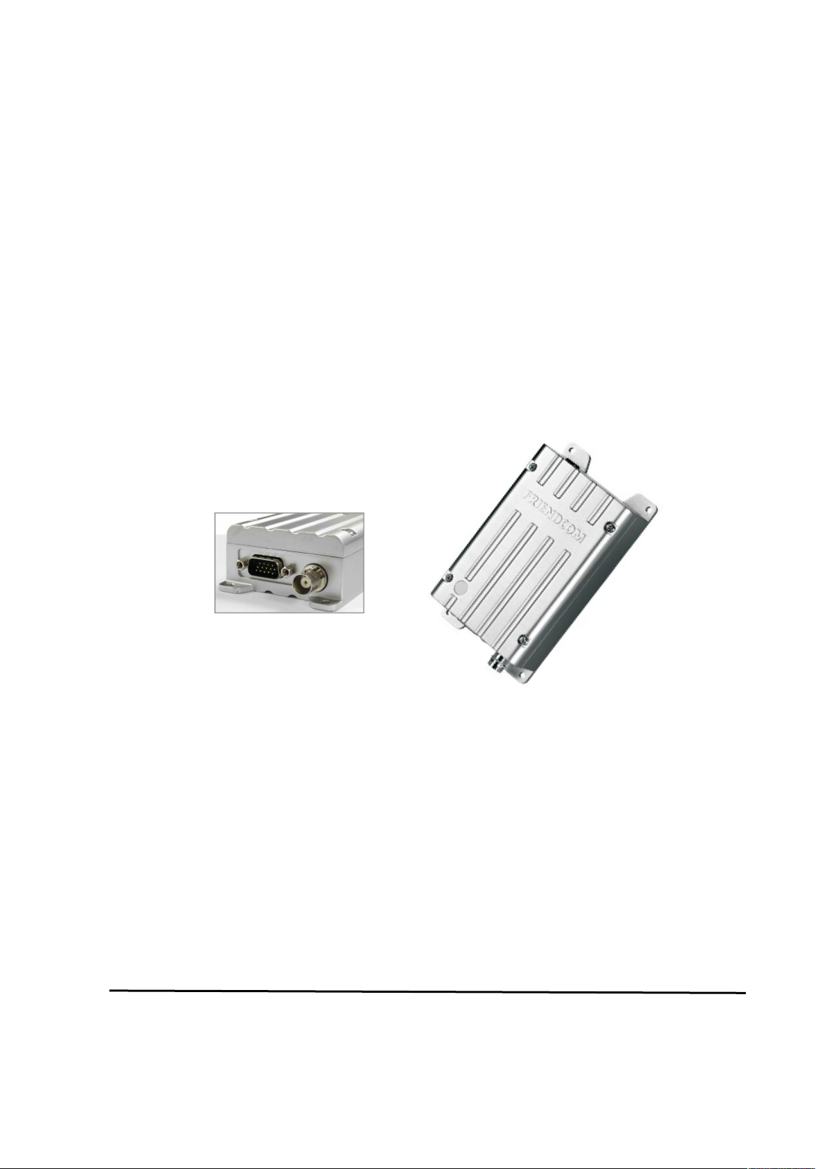
FC-302 Data Radio
User Manual
Address: Comprehensive building, Wanyelong science and technology Park, Liyuan
Industrial Zone, Shiyan Street, Bao'an District, Shenzhen City 518108
P.R.CHINA.
Tel: +86-755-86026600 +86-755- 23230518
Website: http://www.friendcom.cn
SHENZHENG FRIENDCOM TECHNOLOGY DEVELOPMENT CO.,LTD
Page 2

FC-302 Data Radio User Manual
Page 1
Content
1 Product Description...............................................................................................................................................2
2 Technical Specifications....................................................................................................................................... 3
3.1 Power Supply............................................................................................................................................. 5
3.2 RF Channel.................................................................................................................................................5
3.3 Data Baseband Circuit................................................................................................................................6
3.4 Voice Processing Circuit............................................................................................................................7
3.5 Side Tone Circuit....................................................................................................................................... 7
3.6 CTCSS/DCS...............................................................................................................................................8
3.7 Two-Point Balanced Modulation............................................................................................................... 8
3.8 Channel Selection Circuit.......................................................................................................................... 8
3.9 Interfaces.................................................................................................................................................... 9
4 Features............................................................................................................................................................... 15
4.1 Power Save Mode.................................................................................................................................... 15
4.2 CTCSS/DCS.............................................................................................................................................15
4.3 TX Protection...........................................................................................................................................16
4.4 Channel Spacing...................................................................................................................................... 16
4.5 The Field Detection..................................................................................................................................16
4.6 SQ(Squelch) Level...................................................................................................................................16
4.7 De-emphasis Volume...............................................................................................................................16
4.8 Sidetone....................................................................................................................................................16
4.9 Voltage Protection....................................................................................................................................16
4.10 Channel Scan..........................................................................................................................................16
4.11 Channel Select........................................................................................................................................17
5 Maintenance and Repair......................................................................................................................................17
5.1 Dimensions............................................................................................................................................17
5.2 Removing & Replacing the Upper Cover............................................................................................... 18
5.3 Removing & Replacing the Power Board & Modem Board & Shield Plate.......................................... 18
5.4 Removing & Replacing the Main Board................................................................................................. 19
5.5 Repairable/Replaceable Parts List........................................................................................................... 20
6 Accessories Available......................................................................................................................................... 21
Page 3

FC-302 Data Radio User Manual
Page 2
1 Product Description
FC-302 is a synthesized 5-watt FM transceiver module, which is designed for data transportation and
voice communication. For the voice communication, it can support selected pre-emphasis, squelch and audio
amplifier. The radio is PLL(Phase Lock Loop Synthesizer) /microprocessor controlled with optional GMSK,
FFSK modem board. The application of two-point modulation with good low-frequency response in the radio
also makes it a competitive choice for 1200-19200bps rate data application. Compact dimension and wide
range DC support make it flexible to use.
Features:
• CE, FCC& AS/NZS 4295: 2004 certified
• Programmable 16 channels with Dip-Switch
• Configurable power save feature
• Optional external channel configuration
• FSK, FFSK& GMSK modem option
• Frequency step 5KHz/6.25KHz
• CTCSS/DCS
• Support maximum RF data rate: 19200bps
• Fast lock time: 5ms
• SQ programmable via PC
• Pocsag Modulation
• PC programmable & Software tune & Calibration
Applications:
• Industrial telemetry & wireless remote control
• Gas and oil flow monitoring
• Electricity, water and gas utilities
• Earthquake, weather, environmental protection and urban lighting control
• Vehicle tracking and asset tracking systems
• Water monitoring, waste water management and irrigation control
• Railway, police, army automation system
• Aerial defense and fire alarm system
• Wireless Paging system
Page 4
Page 3
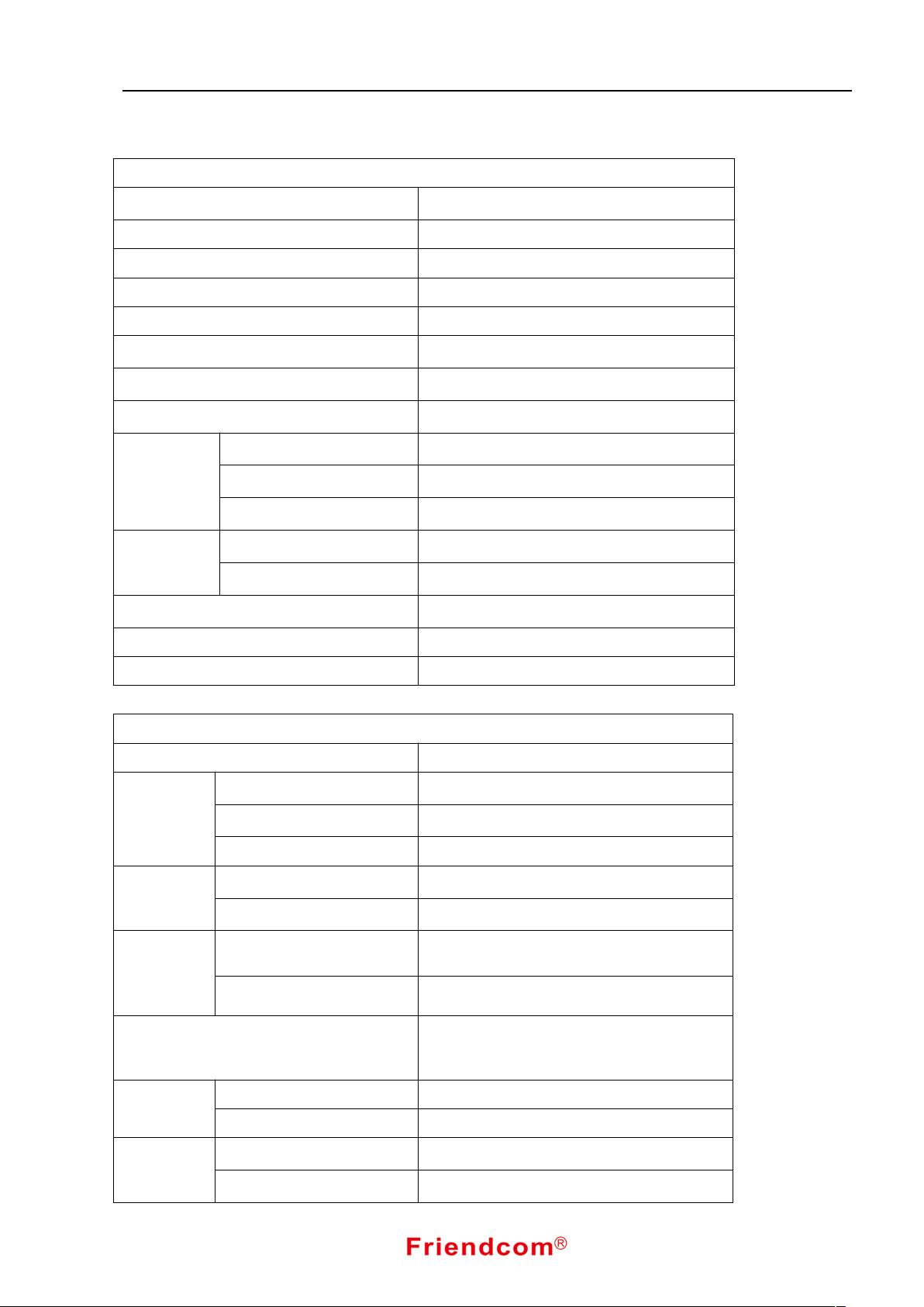
2 Technical Specifications
General Specification
FC-302 Data Radio User Manual
Working Frequency
Channel Spacing 12.5KHz/25KHz Programmable
Modulation Type F3D/F3E
Number of Channels 16
Nominal Working Voltage 12V DC
Extreme Working Voltage
Storage Temperature
Operating Temperature
Standby
Current
Transmit 5 watts RF Power
Consumption
Transmit 1 watt RF Power
TX to RX Attack Time
Lock Time
RX to TX attack time
Frequency Error
Antenna Connector BNC 50Ω
450MHz~490MHz
9.5 V~16V DC
-40℃~+80℃
-30℃~+65℃
<100mA
<1.5A
<1A
<5ms
<5ms
<2.5ppm
External interface DB15/DB9(optional male interface)
Transmitter Specification
RF Power 1W/2W/3W/4W/5W Programmable
25KHz Channel Spacing
Frequency
Deviation
Audio
Response
Adjacent
Channel
Power
Conducted Spurious Emission
Modulation
Sensitivity
12.5KHz Channel Spacing
Subsonic 0.5KHz
25KHz Channel Spacing
12.5KHz Channel Spacing
25KHz Channel Spacing
12.5KHz Channel Spacing
Voice 8~15mV
Data 80~130mV
<5KHz
<2.5KHz
300Hz~3KHz +1/-3dB
300Hz~2.55KHz +1/-3dB
<-70dBc
<-65dBc
<1GHz,<-36dBm
>1GHz,<-30dBm
TX SNR
25KHz Channel Spacing
12.5KHz Channel Spacing
>45dB
>40dB
Page 5
Page 4
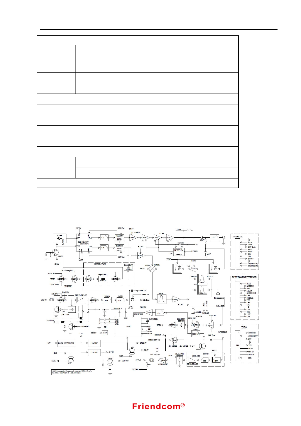
Receiver Specification
FC-302 Data Radio User Manual
RX Sensitivity
(12dB SINAD)
25KHz Channel Spacing
12.5KHz Channel Spacing
25KHz Channel Spacing
<-119dBm Extreme<-115dBm
<-119dBm Extreme<-115dBm
>70dB
ACP
12.5KHz Channel Spacing
Image Rejection
IF Rejection
Spurious Rejection
Intermodulation Suppression
Conducted Spurious Emission
Receiving Audio Distortion
25KHz Channel Spacing
>60dB
>70dB
>70dB
>70dB
>65dB
<-57dBm
<5%
>45dB
RX SNR
12.5KHz Channel Spacing
>40dB
Audio Output Power 0.5W @ 8Ωload
3 Theory of Operation
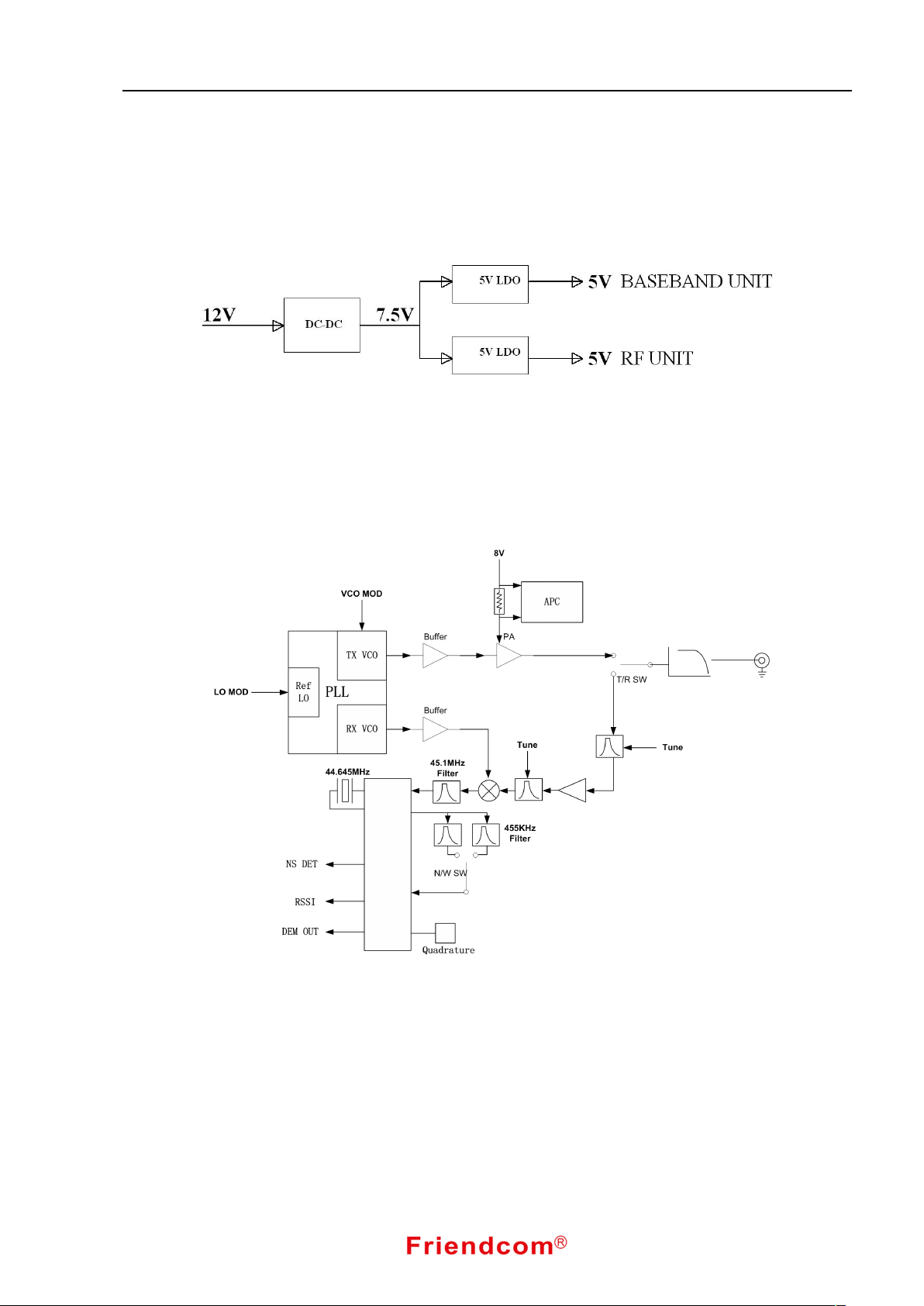
Fig. 1 Overall Circuit Diagram
Page 6
FC-302 Data Radio User Manual
Page 5
FC-302 is comprised of three PCBs (an Mainboard PCB, a Power board and a Modem PCB). These
boards are an 18 pin female and male connector. The digital board is interfaced with external data equipment
through the 15 pin d-sub male connector, which controls the radio and data receiving and sending.
3.1 Power Supply
Fig. 2 Power Supply Diagram
Input 9V~12V will be lowered to 7.5V by DC-DC before it input to the machine. Then it divides into to
circuits through LDO and stabilizes at 5V. One circuit supplies power for RF unit and the other supplies power
for baseband unit. By adopting high-efficiency DC-DC to convert input voltage, the stabilities of all technical
features can be assured.
3.2 RF Channel
Fig. 3 RF Circuit Diagram
FC-302 receiver adopts two-stage intermediate frequency, 45.1MHz and 455KHz. When in RX mode,
the RF signal pass though Antenna Port, Low Pass Filter and RF switching circuit then finally sent to a
Low-noise Band-pass Amplifier Circuit for being magnified. The magnified RF signal and the first local
oscillator signal outputted by VCO will proceed mixing in the first mixer, then produce first intermediate
frequency 45.1MHz. The first intermediate frequency would be filtered by a 45.1MHz crystal band-pass filter.
After buffer amplification it is sent to Pin 16 of IF-PLL demodulation chip. Inside the IF-PLL demodulation
chip the signal will mix with the second local oscillator and produce second intermediate frequency 455KHz.
The 455KHz intermediate frequency will be selected , magnified, limited, and demodulated by the band-pass
filter and then transferred into a baseband signal.
Page 7
FC-302 Data Radio User Manual
Page 6
The low-noise band-pass amplifier adopts electric tuning technology,which can automatically adjust the
center frequency of band-pass filter based on working frequency, to assure a good selectivity and
anti-jamming capability.
About the transmission, the frequency synthesizer(PLL) constituted by voltage-controlled oscillator(VCO),
phase-locked loop chip and reference frequency source produce a carrier signal,which then is sent to radio
frequency power amplifier after buffer amplification. The radio frequency power amplifier finally output a 5W
carrier signal after RF on-off circuit, low pass filter and finally transferred to antenna port.
The power control of RF power amplification adopts automatic current control, by sampling the power
amplifier current,comparing with reference value,auto-adjusting to assure it would stay the same with
reference value. By this step the software programming settings of RF power can be achieved.
3.3 Data Baseband Circuit
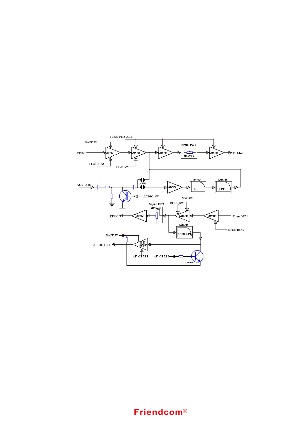
Fig. 4 Data Baseband Circuit Diagram
The circuit mainly works on the amplification of data base band signal, filtering of FSK baseband and
shaping etc.
The data baseband processing circuit supports very low signal frequency, even the DC level and the
amplitude frequency characteristics of wide and flat to meet the high-speed data transmission. The baseband
signal join from the TFSK end and is sent to the modulation circuit after DC level shift, amplification, channel
switch and a gain adjustment circuit .
AUDIO IN offer another data/voice modulation input port, which can transfer audio (data) signals sub
3KHz, adopting AC coupling with narrow frequency response, appropriate for low-speed data modulation.
In Rx mode, the intermediate frequency demodulation chip output baseband signal. The baseband signal is
amplified and go through DC level shift, narrowband and wideband switching, then is sent to the variable
gain amplifier. After that baseband signal containing DC component is output from the RFSK terminal. The
other signal is sent to the low pass filter to select sub 3KHz audio signal (data). After controllable switch circuit,
audio(data) output from filter or data signal shaped into a square wave signal can be output directly in AUDIO
OUT, appropriate for low speed data transmission.
Page 8
Page 7
3.4 Voice Processing Circuit
FC-302 Data Radio User Manual
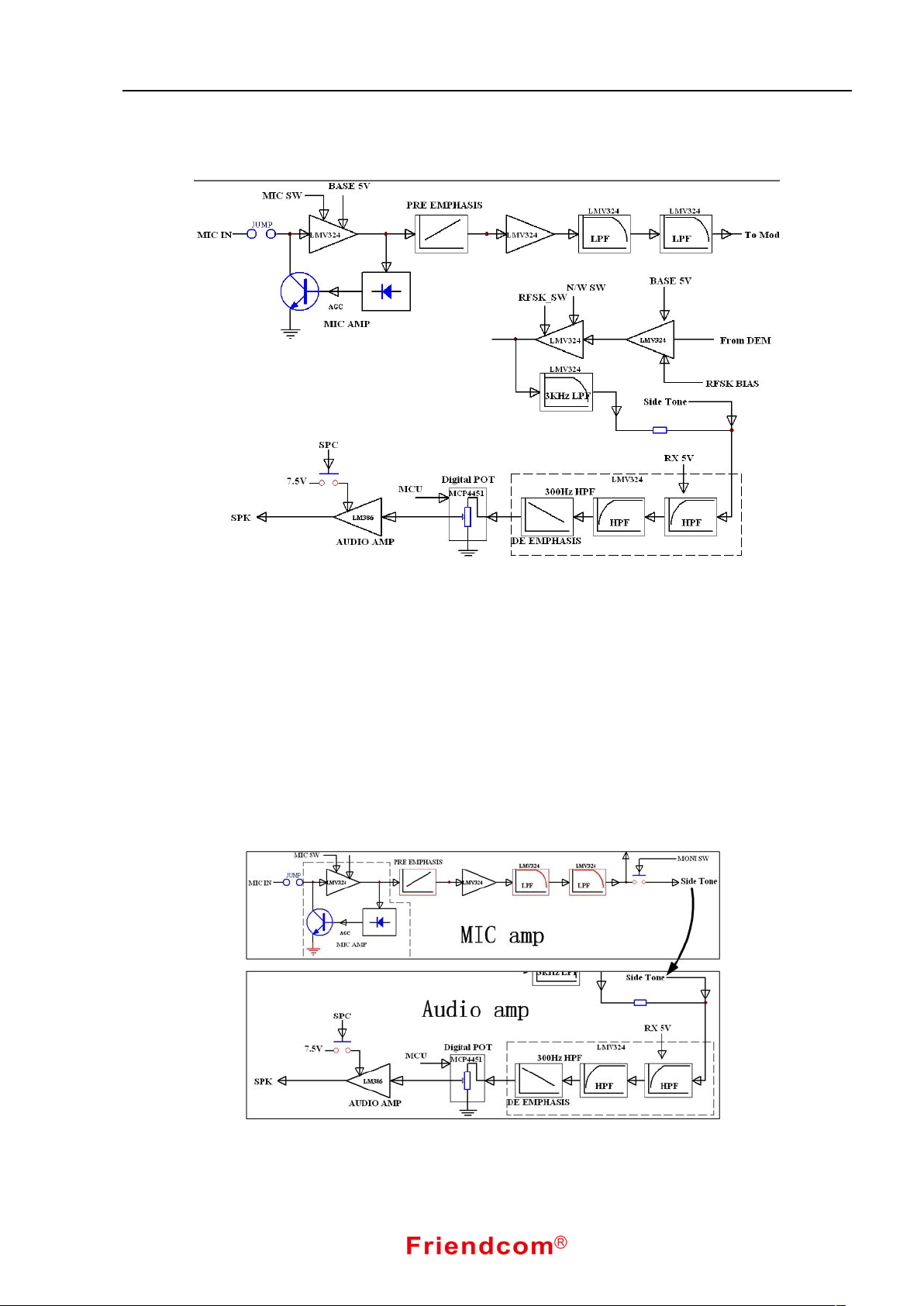
Fig.5 Voice Processing Block Diagram
When in TX mode, speech signal is transferred from the MIC IN to amplifier with automatic gain control
function for amplification , and then is sent to the modulator through the audio frequency pre- emphasis circuit,
a limiter circuit and low pass filter.
When in RX mode, the intermediate frequency demodulation chip output baseband signal. The baseband
signal is amplified and go through DC level shift, narrowband and wideband switching. the filter is consist of
3KHz low-pass filter and 300Hz high-pass filter, mainly used for tone and high-frequency noise filtering to
improve signal to noise ratio(SNR). Then the audio signal is output from the SPK after volume controls and
power amplifier.
3.5 Side Tone Circuit
Fig. 6 Sidetone Block Diagram
When sidetone function is enable, signal amplified by MCU will be separated. One part of signal will be
Page 9
FC-302 Data Radio User Manual
Page 8
transferred to the audio power amplifier to drive trumpet for voice. Then users can hear his own voice when
sending the voice.
3.6 CTCSS/DCS
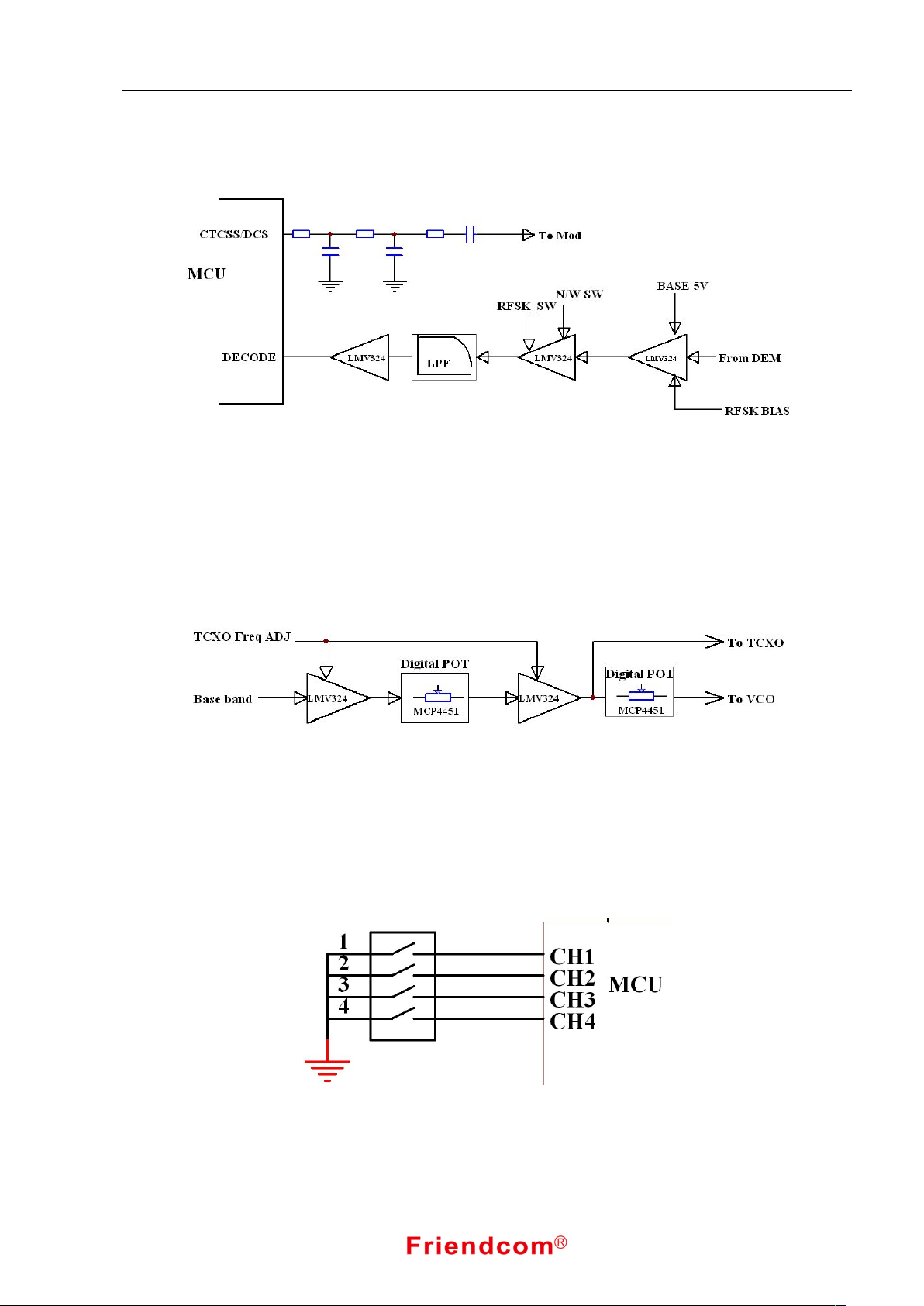
Fig.7 CTCSS/DCS Processing Block Diagram
CTCSS/DCS encoding and decoding is completed by the MCU. When radio is in TX mode, subaudio sent
from the MCU is directly transferred to the carrier modulator-carrier modulation via second-order RC filter.
When the radio in Rx mode, baseband signal output form intermediate-frequency demodulator chip process the
audio filtering after the DC level shift and switching between wideband and narrowband. The audio filter is an
300Hz low pass filter and select sub audio signal sent to the MCU for decoding.
3.7 Two-Point Balanced Modulation
Fig.8 Two-point Balanced Modulation Diagram
Two-point balanced modulation is used when carrier is modulated by baseband signal. That is one signal
modulate reference frequency source of the frequency synthesizer, another signal modulate the VCO frequency.
Two-point modulation have characteristics of linearity and bandwidth etc. The radio two-point modulation uses
DC coupling mode, making modulation signal low end frequency response smoother.
3.8 Channel Selection Circuit
Fig.9 Channel Selection Diagram
The radio’s 16 channels can be select by inner dip switch (4 bits). MCU reads the status of the switch to
select wanted channel by changing dip switch(4 bits). Besides hardware control, software control is also
available when banning dip switch.
Page 10
Page 9
3.9 Interfaces
Mainboard interface:
FC-302 Data Radio User Manual
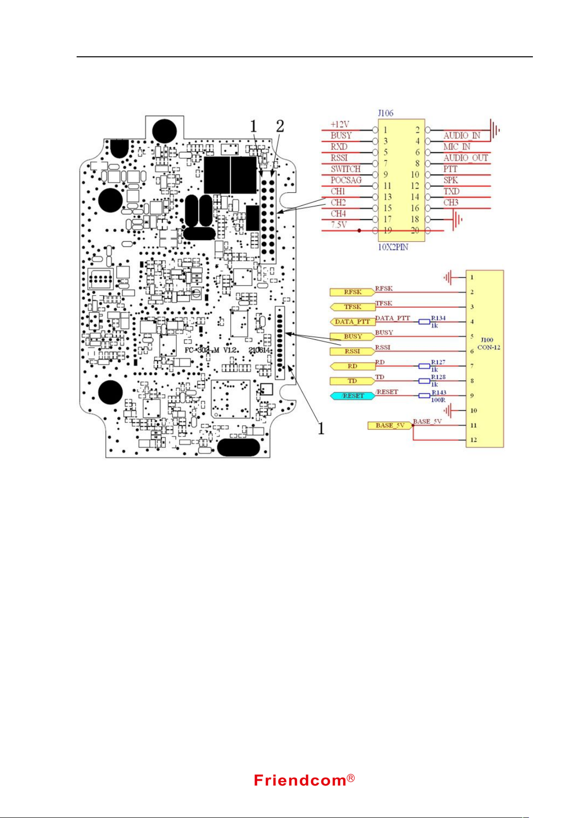
Fig.10 Mainboard Interface Description
There are two external interfaces in mainboard. One is J106 and connected to the Power board,
transferring available I/O signal to the user through the Power. The other is J100 and connected with modem,
customers can develop appropriate modem according to specific requirement.
Power Board (PWR):
Page 11
FC-302 Data Radio User Manual
Page 10
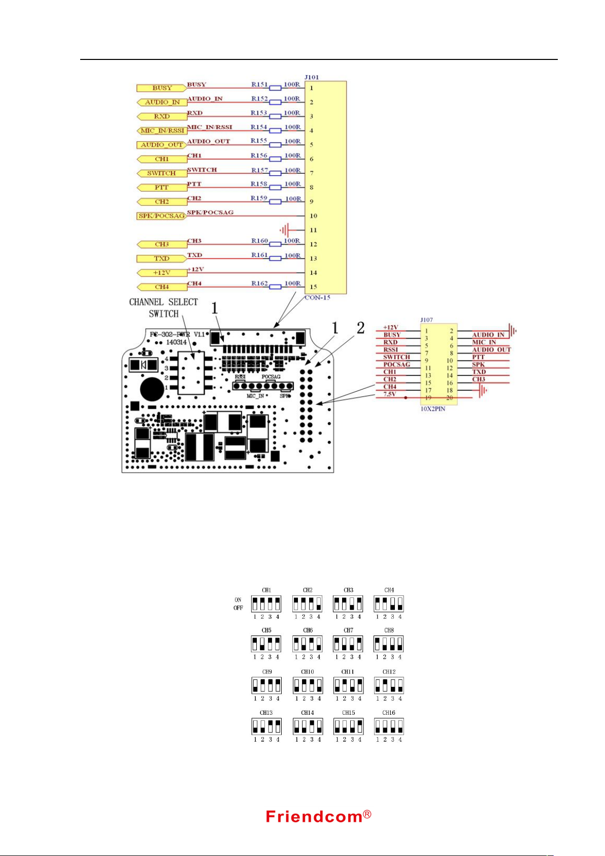
Fig.11 Power Board Interface Description
Power board J107 is docked with J106, J101 is connected to the external interface (DB9/DB15). Customer
can customize and match corresponding interface connector according to the functional requirements.
Channel selection switch provides 16 channels for users to choose. The switch encodes the channel
number, selected into 4-bit binary code, the binary code plus one equal to the channel number. Once located
change the Dip switch to select wanted channel according to the channel dip switch chart (See fig.12).
Fig. 12 Channel Dip Switch Chart
Page 12
Page 11
V23 Modem Interface:
FC-302 Data Radio User Manual
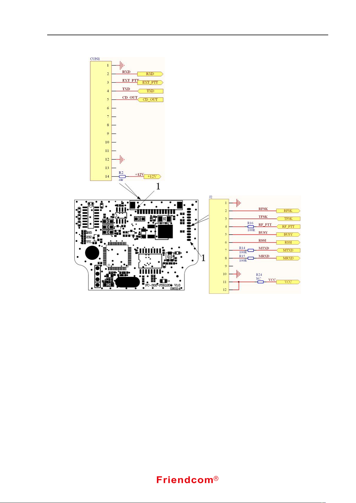
Fig.13 V23 Modem Interface Description
Modem is designed for data modulation and demodulation. J2 is docked with J100 and CON 1 is
connected to Pin 14 in radio external interfaces (DB15).
External interfaces:
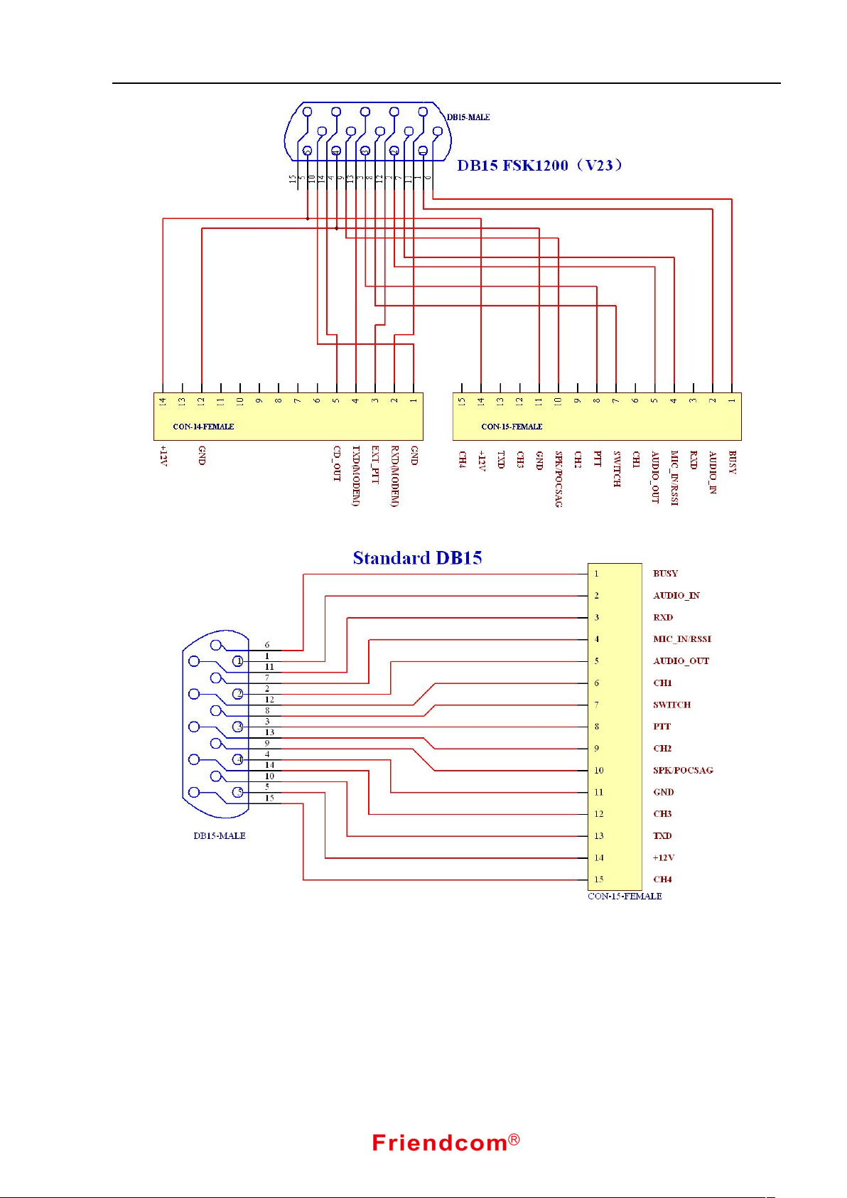
Users can choose external interfaces below according to the specific requirements.
Page 13
FC-302 Data Radio User Manual
Page 12
Fig.14 DB15 FSK1200 (V23) Interface Pin Assignment
Fig.15 DB15 Interface Pin Assignment
Page 14
FC-302 Data Radio User Manual
Page 13
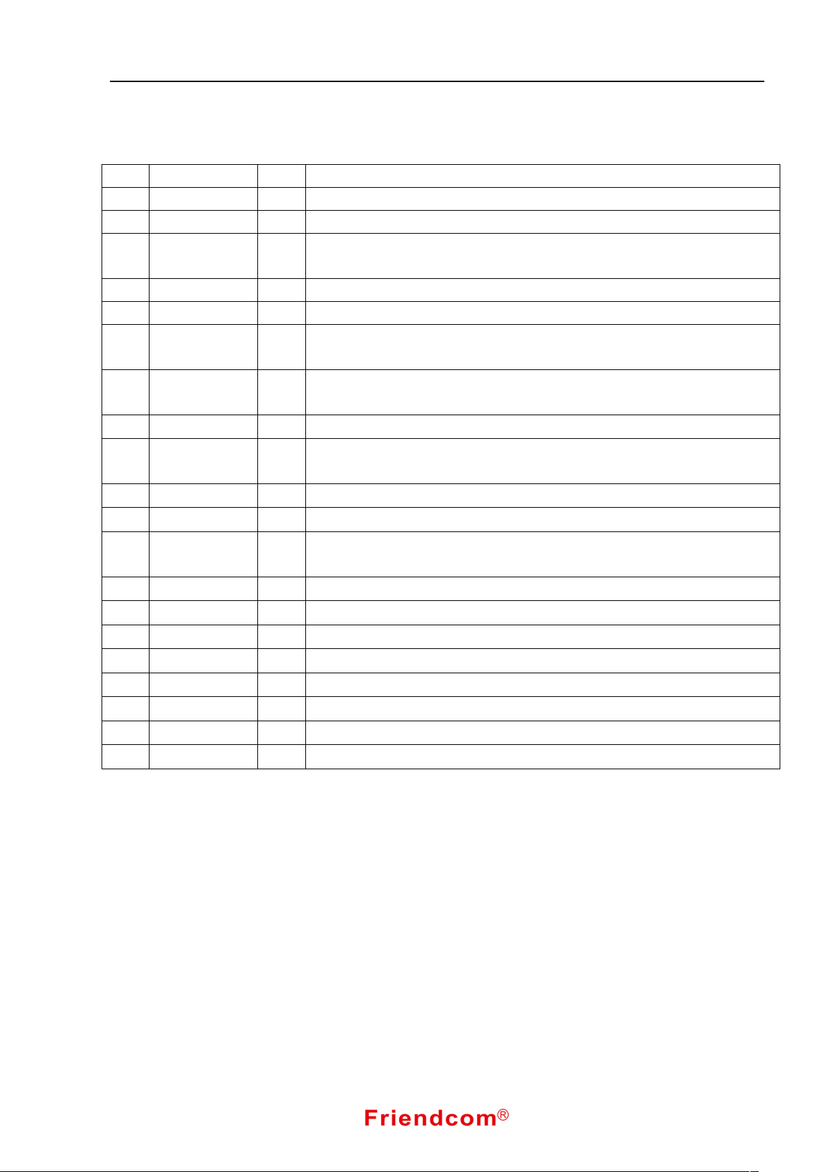
Baseband signal input end for the modulation in transmitter, 100mVrms,sent
from modem to mainboard
+5V power supply,transferred from mainboard to modem, Maximum current
50mA.
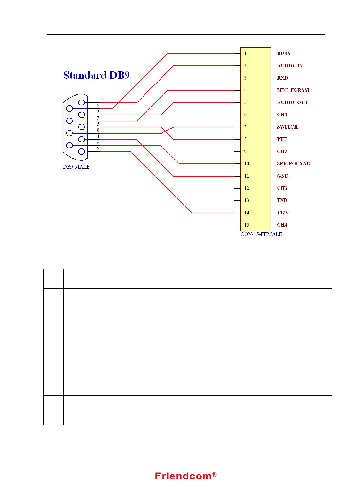
Fig.16 DB9 Interface Pin Assignment
Mainboard connect to modem(J100---J2)
No. Name Type Description
1 GND I/O Ground
2 RFSK O
The output signal after the intermediate frequency demodulation in receiver.
200mVrms,sent to modem
3 TFSK I
4 DATA_PTT I Data TX control. Active when low level. Control the mainboard via modem
BUSY output. low level when receiving (Default). Sent from mainboard to
5 BUSY O
modem
6 RSSI O Received field strength output, transferred from mainboard to modem
7 RD I Data communication serial port from modem to mainboard
8 TD O Data communication serial port from mainboard to modem
9 /RESET I Reset control, low level when resetting. Control the mainboard via modem
10 GND I/O GND
11
BASE_5V O
12
Page 15
FC-302 Data Radio User Manual
Page 14
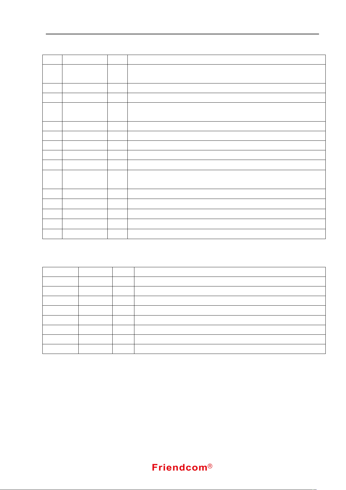
Mainboard is connected to power board(J106--J107)
No. Name Type Description
1 +12V I 12V power supply,used for voltage monitoring
2 GND I/O GND
3 BUSY O
BUSY output, dent from mainboard to power board. The default output low
level
4 AUDIO_IN I Audio input, Modulation sensitivity is 100mW
5 RXD I RX data
Microphones signal input from power board to mainboard. Modulation
6 MIC_IN I
7 RSSI O
sensitivity is 10mW.
Received field strength indicator for DC voltage output, the stronger the
signal ,the higher voltage is. Transferred from mainboard to power board
8 AUDIO_OUT O Audio output, 100mW, transferred from mainboard to power board
9 SWITCH I
Programmable switch, Configurable specific function options. Input port in
mainboard.
10 PTT I
11 POCSAG I
TX control. low level when transmitting from power board to mainboard.
POCSAG modulation input from power board to mainboard.
Speech output, able to drive 8 ohm speaker. Transferred from mainboard to
12 SPK O
13 CH1 I
14 TXD O
15 CH2 I
16 CH3 I
17 CH4 I
18 GND I/O
19 7.5V I
20 7.5V I
power board
Programmable CH1
TX data
Programmable CH2
Programmable CH3
Programmable CH4
GND
Power supply from power board to mainboard
Power supply from power board to mainboard
Page 16
FC-302 Data Radio User Manual
Page 15
Power board connect to external interface(J101--DB9 or DB15)
No. Name Type Description
1 BUSY O
2 AUDIO_IN I Audio input, Modulation sensitivity is 100mW
3 RXD I RX data
4 MIC_IN/RSSI I/O
5 AUDIO_OUT O Audio output, 100mW, transferred from mainboard to power board
6 CH1 I Programmable CH1
7 SWITCH I Programmable switch, configurable specific function options
8 PTT I TX control, low level when transmitting from power board to mainboard.
9 CH2 I
10 SPK/POCSAG O/I
11 GND I/O
12 CH3 I
13 TXD O
14 +12V I
15 CH4 I
BUSY detect output, Sent from mainboard to power board. The default output
low level. Also able to work as simulated serial and data transmission port.
Microphones signal input. Modulation sensitivity is 10mW. A jumper in
power board can be defined as received field strength signal.
Programmable CH2
Speech output, able to drive 8 ohm speaker, a jumper in power board can be
defined as POCSAG modulation input port
GND
Programmable CH3
TX data
+12V,supply power for whole radio
Programmable CH4
V23 modem connect to external interface (CON1---DB15)
No. Name Type Description
1 GND I/O GND
2 RXD I RX Data
3 EXT_PTT I TX control. Low level: modem in TX status
4 TXD O TX Data
5 CD_OUT O Carrier detect control. Default output low level when receiving carrier
6~11、13 NC -- Not used
12 GND I/O GND
14 +12V I Power supply input
4 Features
4.1 Power Save Mo d e
When user enable power save mode, the radio will work into beat status to save the energy. If detect useful
signal, the radio will start to work normally. If no useful signal detected, the radio will get into beat status.
Heartbeat interval can be programmed via PC. However, real time communication will be slightly affected.
4.2 CTCSS / D C S
When enabled, receiver only can receive useful RF signal with the same CTCSS/DCS code of the
Page 17

FC-302 Data Radio User Manual
Page 16
transmitter to avoid interference from useless signal. The CTCSS/DCS code can be programmed by PC
software. For fast lock time, the CTCSS/DCS is not available for high speed data transmission.
4.3 TX Protec t i o n
This feature, when enabled, limits the amount of time that the radio can continuously transmit for
protecting the radio from block of the channel and damage on radio which is caused by sustained transmission.
In TX mode, if PTT is effective all through and exceed set time, radio will stop transmitting automatically until
restart the PPT again. The time can be set by PC software.
4.4 Chann e l Spa c i n g
The radio is capable of programmable channel spacing, having 12.5KHz or 25KHz channel spacing. The
minimal frequency band is 6.25KHz.
4.5 The Fiel d De t e c t i on
In TX mode, the radio can quickly detect the strength of useful RF signal and show the strength by analog
voltage after calculation and analysis of MCU. Stronger signal means higher output voltage. User can also read
the field strength by serial command.
4.6 SQ (S q u e l c h ) Le v e l
Five SQ level is set in the radio and can be selected by PC software.
Level 0 is for fully open mute. The audio signal will continuously transmit. Other levels are shown as
below:
Level 1:0.15uV
Level 2:0.25uV
Level 3:0.35uV
Level 4:0.45uV
Level 5:0.55uV
4.7 De-e mp h a s i s Vo l u m e
The radio output voice via SPK Pin with 10 level volume. Users are able to choose appropriate volume for
the connected speaker in this feature by PC software. The default volume is 6. The minimal volume is 0 and the
maximum is 9.
4.8 Side to n e
This feature, when enabled, transmitted MIC signal will be output from SPK port after partly power
amplifier and user can hear his or her own voice. The feature can also be set via PC software.
4.9 Volt a ge Pr o t e c t i on
When enabled, the radio will automatically stop working if the power supply is lower than rated low
voltage and be in low-consumption status. Once the power supply become higher than rated high voltage, the
radio will start to work again. User can set the rated voltage via PC software.
4.10 Chann e l Sc a n
The radio enable to detect the channels by initiate scanning mode. Scanning mode is optional and
programmable. This PC software allows user to decide scan mode and establish channel scanning sequence. 4
scan modes are provided in “Option” and shown as below
0 ---------normal scan with carry only
1 ---------normal scan, Carry with tone
2 ---------priority scan, Carry only
Page 18
FC-302 Data Radio User Manual
Page 17
3 ---------priority scan, carry with tone
4.11 Chann e l Sel e c t
Radio’s 16 channels can be selected by inner dip(4) switch(HW) on power board or serial command
inputted from our PC software(SW). Only in SW control mode, channel can be selected by PC software in
“Channel” feature.
5 Maintenance and Repair
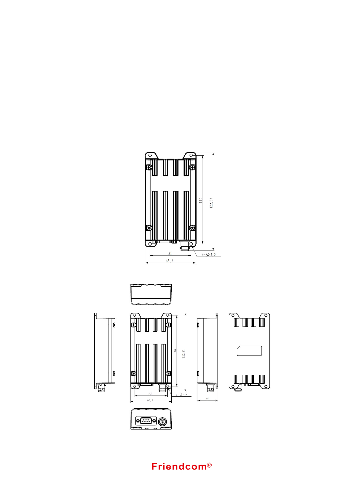
5.1 Dimensions
Fig.17 Top View
Fig. 18 Exterior View
Page 19
FC-302 Data Radio User Manual
Page 18
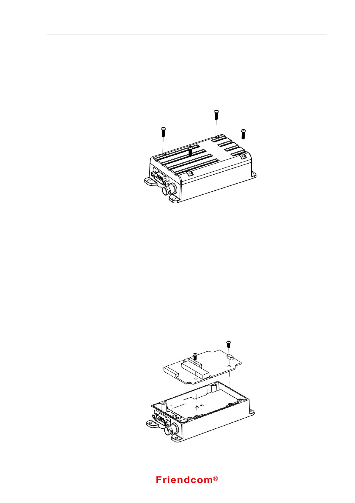
1. Unscrew the four upper cover mounting screws located on the upper cover of radio
1. Reserve the steps taken to remove the Main board Assembly & Power board & Shield Plate.
5.2 Removing & Replacing the Upper Cover
Removing the Upper Cover
To replace the Upper Cover
1. Reserve the steps taken to remove the Upper Cover.
Fig. 19-Upper Cover Removal
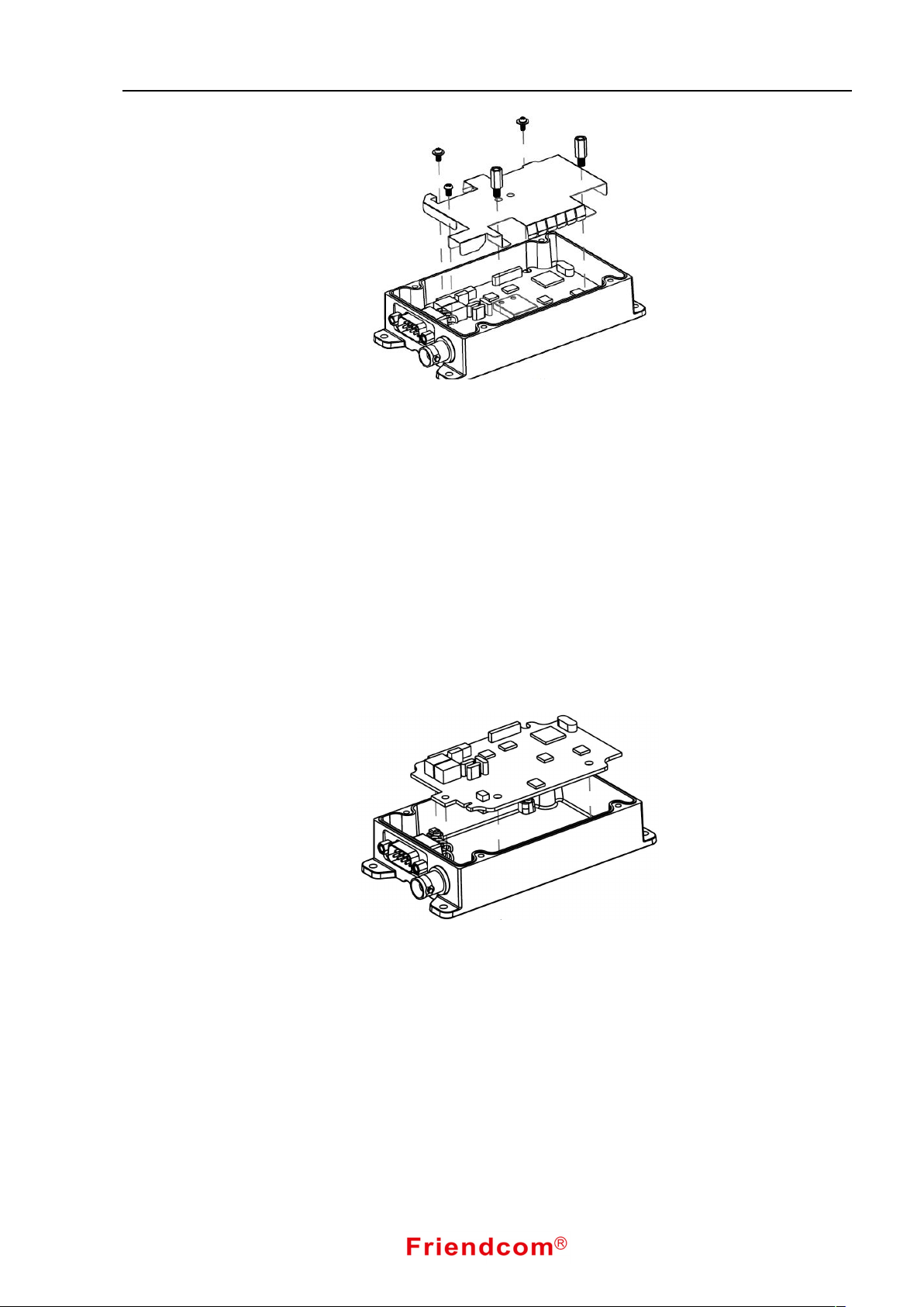
5.3 Removing & Replacing the Power Board & Modem Board & Shield Plate
Removing the Power Board & Modem Board Assembly & Shield Plate
1 Removing the Upper Cover (refer to Removing & Replacing the Upper Cover )
2 Disconnect the DB15 pin connector on CON14.
3 Unscrew the 4 monting screws.
4 Remove the Main Board Assembly.
5 Remove the Shield Plate.
To replace the Main board & Power board Assembly:
Fig. 20-Power board & Modem board Assembly Removal
Page 20
FC-302 Data Radio User Manual
Page 19
Fig. 21-Shield Plate Assembly Removal
5.4 Removing & Replacing the Main Board
1 Remove the Upper Cover (refer to Removing & Replacing the Upper Cover )
2 Remove the Power board, Modem Board & Shield Plate
(refer to Removing the Power board & Modem Board Assembly & Shield Plate)
3 Unscrew the 4 mounting standoffs.
4 Unsolder the antenna connector cable.
5 Remove the Main Board Assembly.
To replace the Main Board Assembly:
1. Reverse the steps taken to remove the Main Board Assembly.
Fig. 21-Main Board Removal
Page 21
FC-302 Data Radio User Manual
Page 20
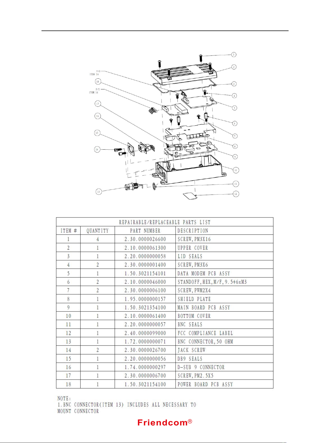
5.5 Repairable/Replaceable Parts List
Fig. 22 Exploded View
Page 22

FC-302 Data Radio User Manual
Page 21
6 Accessories Available
Please contact the Friendcom sales team for accessory information.
Tel: +86 755 23230544
 Loading...