

Page 1

FC-301/D RF Link Module
USER MANUAL
SHENZHEN FRIENDCOM TECHNOLOGYDEVELOPMENT CO.,LTD
ADD: 6/F, 17 Building , Guangqian Industrial Park, Longzhu Road, Xili Town,
Nanshan, Shenzhen City 518055 P.R.CHINA.
TEL: +86-755-86026600 +86-755-86026192 FAX: +86-755-86026300
E-MAIL: [email protected]
WEBSITE: www.friendcom.com
Page 2

- 1 -
MANDATORYSAFETY INSTRUCTIONSTO INSTALLERSAND USERS
Use Only manufacturer or dealer supplied antennas.
Antenna minimum safe distance: 35 cm.
Antennas used for this transmitter must not exceed an antenna gain of 3 dBi.
The FCC (Federal Communications Commission) has adopted a safety
standard for human exposure to RF energy which is below the OSHA
(Occupational Safety and Health Act) limits.
Antenna mounting: The antenna supplied by the manufacturer or radio dealer
must not be mounted at a location such that during radio transmission, any
person can come closer than the above indicated minimum safe distance to the
antenna (i.e. 35cm).
To comply with current FCC RF Exposure limitations, the antenna must be
installed at or exceeding the minimum safe distance indicated above, and in
accordance with the requirements to the antenna manufacturer or supplier.
Vehicle installation: The antenna can be mounted at the center of a vehicle metal
roof or trunk lid if the minimum safe distance is observed.
Antenna substitution: Don’t substitute any antenna for the one supplied or
recommended by the manufacturer or radio dealer. You may be exposing
person(s) to excessive radio frequency radiation. You may contact your radio dealer
or the manufacturer for further instructions. Warning
Maintain a separation distance from the antenna to person(s) at least 108cm.
Page 3

- 2 -
Caution:
Changes or modifications not expressly approved by the party responsible for
compliance could void the user's authority to operate the equipment.
This device complies with part 15 of the FCC Rules. Operation is subject to the
following two conditions: (1) This device may not cause harmful interference, and (2)
this device must accept any interference received, including interference that may
cause undesired operation.
Note: This equipment has been tested and found to comply with the limits for a
Class B digital device, pursuant to part 15 of the FCC Rules. These limits are
designed to provide reasonable protection against harmful interference in a
residential installation. This equipment generates, uses and can radiate radio
frequency energy and, if not installed and used in accordance with the instructions,
may cause harmful interference to radio communications. However, there is no
guarantee that interference will not occur in a particular installation. If this
equipment does cause harmful interference to radio or television reception, which
can be determined by turning the equipment off and on, the user is encouraged to try
to correct the interference by one or more of the following measures:
Reorient or relocate the receiving antenna.
Increase the separation between the equipment and receiver.
Connect the equipment into an outlet on a circuit different from that to which the
receiver is connected.
Consult the dealer or an experienced radio/TV technician for help.
Page 4

- 3 -
Note: The manufacturer is not responsible for any radio or tv interference caused by
unauthorized modifications to this equipment. Such modifications could void the
user’s authority to operate the equipment.
Page 5

- 4 -
TABLE OF CONTENTS
TABLE OF CONTENTS ......................................01
..
INTRODUCTION
...........................................02
FEATURES
................................................02
SPECIFICATION
...........................................02
WIRING DIAGRAM
.........................................8
TROUBLESHOOTING GUIDE
................................10
FACTORYDEFAULT SETTING
..............................11
INTRODUCTION
Page 6

- 5 -
The FC-301/D RF Link Modules from Friendcom utilizes the latest technology
in its design and manufacturing. It’s PLL (Phase Lock Loop Synthesizer) /
microprocessor controlled, and offers one to five watts of power with 16 channel
capability. Multiple functions including AC audio coupling, 1200 to 9600 baud
rates GMSK and FSK modulation capability are standard in this fully
programmable wide bandwidth RF Link Module units.
FEATURES
●
16 Channels
●
1 - 5 Watt Programmable RF Output
●
12.5 kHz Programmable Channel Spacing
SPECIFICATIONS
GENERAL
Equipment Type…………………………………Data Radio
Frequency Band …………………………………………...UHF
Channel Spacing………………………………12.5KHz programmable
RF Output Power……………………………….1W - 5W Programmable
Modulation type ………………………………..8K5F3E
Page 7

- 6 -
Intermediate Frequency………………………… 45.1MHz & 455KHz
Number of Channels…………………………….16
Frequency Source ……………………………….Synthesizer
Operation Rating…………………………………Intermittent
5:5:90 ( TX: RX: Standby )
Power Supply ……………………………………12.5VDC Nominal Voltage
Temperature Range
Storage………………………………………from –40°C to +80°C
Operating……………………………………from –30°C to +60°C
Current Consumption
Standby (Muted) ……………………………≤40mA
Transmit 5 Watts RF Power …………………< 1.5A
Transmit 1 Watt RF Power…………………..<0.8A
Dimensions……………………………..(120mm)Lx (60mm)W x (20mm)H
Weight……………………………………………..≤150 grams
TRANSMITTER
Sustained Transmission…………………………… Nominal conditions
Page 8

- 7 -
Time: 5 10 30 sec
Power: >95% >95% >90%
Frequency Error…………………………………..±2.5 ppm
Frequency Deviation:
12.5kHz Channel Spacing……………………
≤±
2.5kHz,
Audio Frequency Response…………………….Within +1/-3dB of 6dB octave
@300Hz to 2.55kHz for 12.5kHz C.S
Adjacent Channel Power
12.5kHz ………………………………………< 60 dBc @ Nominal Condition
< 55 dBc @ Extreme Condition
Conducted Spurious Emission …………………….< -36 dBM
Modulation Sensitivity……………………………. 100mV RMS@60% peak Dev.
Hum & Noise:
12.5kHz Channel Spacing………………..……>36 dB (with POSPH)
Modulation Symmetry ……………………………..<10% Peak Dev@1kHz input
for nominal dev +20dB
Load Stability……………………………………No osc at >= 10:1 VSWR all
phase angles and suitable antenna
No destroy at >= 20:1 all phase angle
RECEIVER
Page 9

- 8 -
Sensitivity(12dB Sinad) ………………………….UHF<-117 dBm,
VHF<[email protected]
Amplitude Characteristic………………………….<±3dB
Adjacent Channel Selectivity:
12.5kHz Channel Spacing…………………….≥60dB@Nom.
Spurious Response Rejection………………………70dB
Image Response…………………………………… > 70 dB
IF Response ………………………………………. >70 dB
Others………………………………………………> 70 dB
Intermodulation Response Rejection………………≥65 dB
Conducted Spurious Emission @ Nominal Conditions………<-57 dBm
AF Distortion ………………………………………………....<5% @ Nom.,
<10%@ Extreme Condition
RX Hum & Noise:
12.5kHz CP ………………………………………..…< 40dB with PSOPH
Receiver Response Time …………………………….< 20ms
Squelch Opening sensitivity: ………………………-118dBm
Squelch Closing sensitivity ………………………..-121dBm
SquelchAttack Time:
RF Level at Threshold ………………………… <40ms
RF Level at Threshold +20dB…………………<30ms
L.O. Frequency Temperature Stability…………….1 st <2.5 ppm,
Page 10

- 9 -
2 nd <10 ppm for –30°C to +60°C
L.O. FrequencyAging Rate………………………….±2 ppm/year
REFERENCE CRYSTAL
Frequency…………………………………………………. 13MHz
Temperature Characteristic……………………………+/- 2.5PPM
from –30°C to +60°C
Aging Rate…………………………………….< 2ppm/yearin 1 st year
<1ppm/year thereafter
Lock Time …………………………………………………<10 ms
TX to RX ………………………………………………… < 20 ms
RX to TX ………………………………..……………….. < 25 ms
ENVIRONMENTAL ( performance without degradation unless stated)
Temperature……………………………………………… deg C
Operating………………………………………………….-30° to +60°C
Degradation Specified@Extreme
Storage ……………………………………………………-40°C to +80°C
Recharging ………………………………………………-10 to +55
ESD………………………………………………………. 20kV (C-MIC >= 15kV)
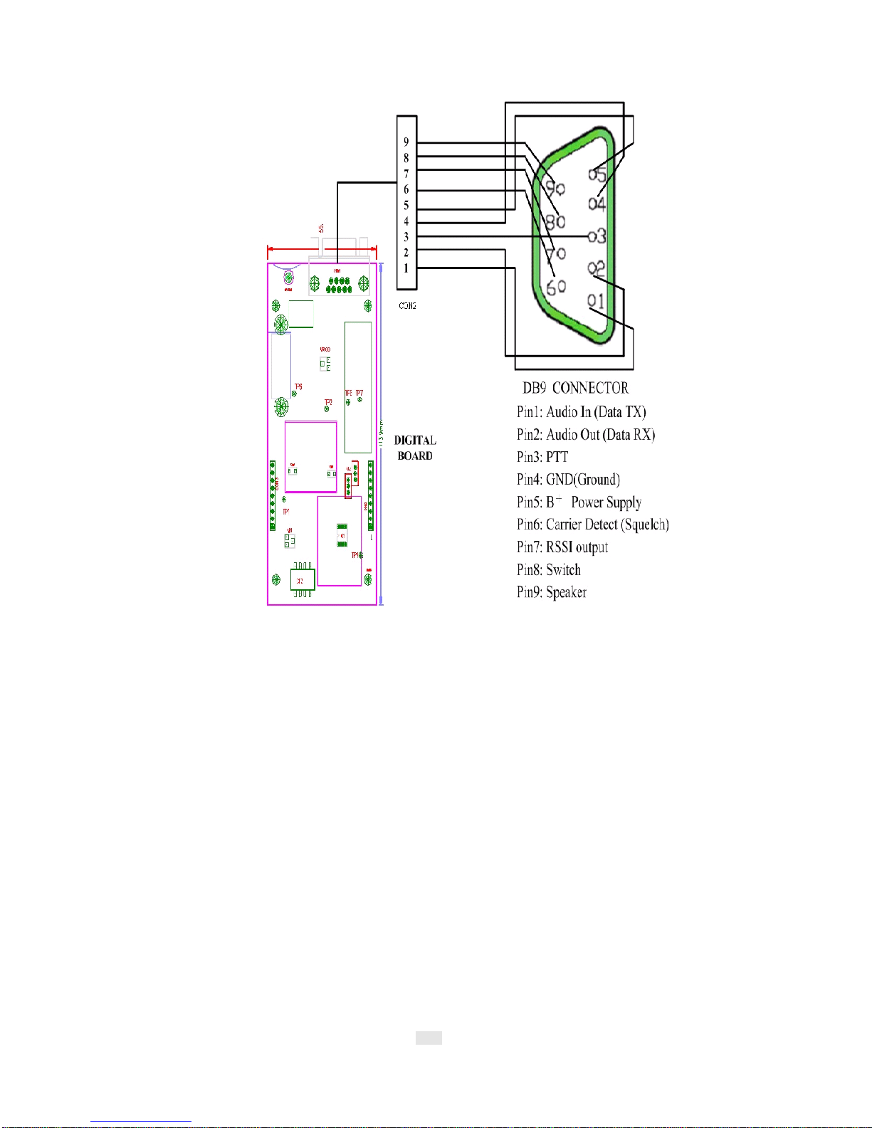
WIRING DIAGRAM
Page 11
- 10 -
Page 12
- 11 -
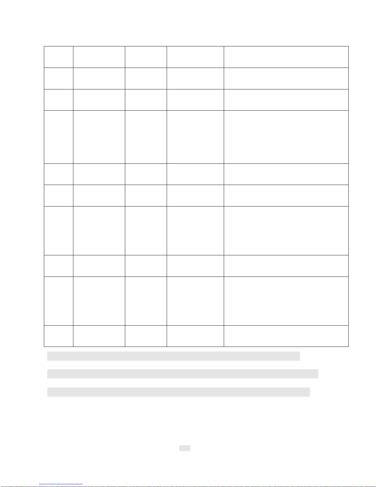
When Pin 8 is connected to GND(0V), the radio is in program mode. The
parameters of the radio can be changed in this mode. When Pin 8 is connected
to 5V voltage, the radio works normally in transmission or receiving status.
Pin Function Type Range Description
Pin 1 Audio in(Data
TX)
Input 200VP-P ------
300VP-P
ExternalModulation Input
Pin 2 Audio out (Data
RX )
Output 150mV-250mV Demodulation Output
Pin 3 PTT Input 0 V/+5V
TransmitEnable
0V - Radio in Transmit status
5V - Radio in receive
status(Default )
Pin 4 GND GND 0V GND
Pin 5 B+ V+ 10-15V Power Supply(+12.5V typical )
Pin 6 SQ Output Open/Short RF Carrier Detect
Open -- low level,
Short -- high level (Default).
Pin 7 RSSI Output 0.8V-2.2V
Pin 8 Switch Input 0V/5V
Programming Enable
0V - Radio programmable
5V - Radio work (Default )
Pin 9 Speaker Output 8ohm /0.5W
Page 13
- 12 -
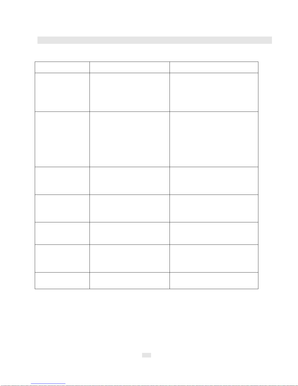
TROUBLE SHOOTING GUIDE
SYMPTOM S CAUSES COUNTERMEASURES
Unit does not work
1.No power incomplete
connection
2. No input voltage of 5V or 8V
3. CPU does not work
4. EEPROM fail
5. Channel error
6. PLL error
1.Check COM1 connection
2. Check IC500、IC504
3. Check IC510
4. Check IC502
5. Check CF3
6. Check TCXO、VCO、PLL IC
Bad RX Sensitivity
1.Antenna signal short-circuit
2.Antenna signal open-circuit
3. Bad electronic turner
4. Defective high frequency
amplifier
5. Bad mixer
6. Local signal amplitude
become small
7. Bad 1stand 2
nd
intermediate
frequency
1. Check D106 D107
2. Antenna loose weld
3. Check L23 L24 L25 L26
4. Replace Q15
5. Check IC3 T3 T4
6. Check D103 Q111
7. Check XF1 XF2 IC2
Defective RX
1. No output signal
2. Bad signal waveform
3. Bad stability of VCO
1. Replace IC801
2. Check U2 c412 c404
3. Check component of VCO
PLL Error
1. TCXO frequency error
2. Bad stability of VCO
3. PLL can’t be locked
1.Check crystal oscillator of TCXO
2.Check the component of
TX/RXVCO
3. IC301 Q321 Q320 C327
Low TX Power 1. Bad amplifier circuit
2. BadAPC circuit
1. Replace IC102
2. Check D102 IC1
No TX Power
1. No power on TX
2. No signal on driver
3. Bad amplifier circuit
4. BadAPC circuit
1. Check Q502 Q503
2. Check Q1 Q2 D101
3. Check IC102 D102
4. Check IC1
No Modulation 1. No input signal
2. No TX signal
1. Check IC801
2. Check U1 R403 R404
Page 14
- 13 -
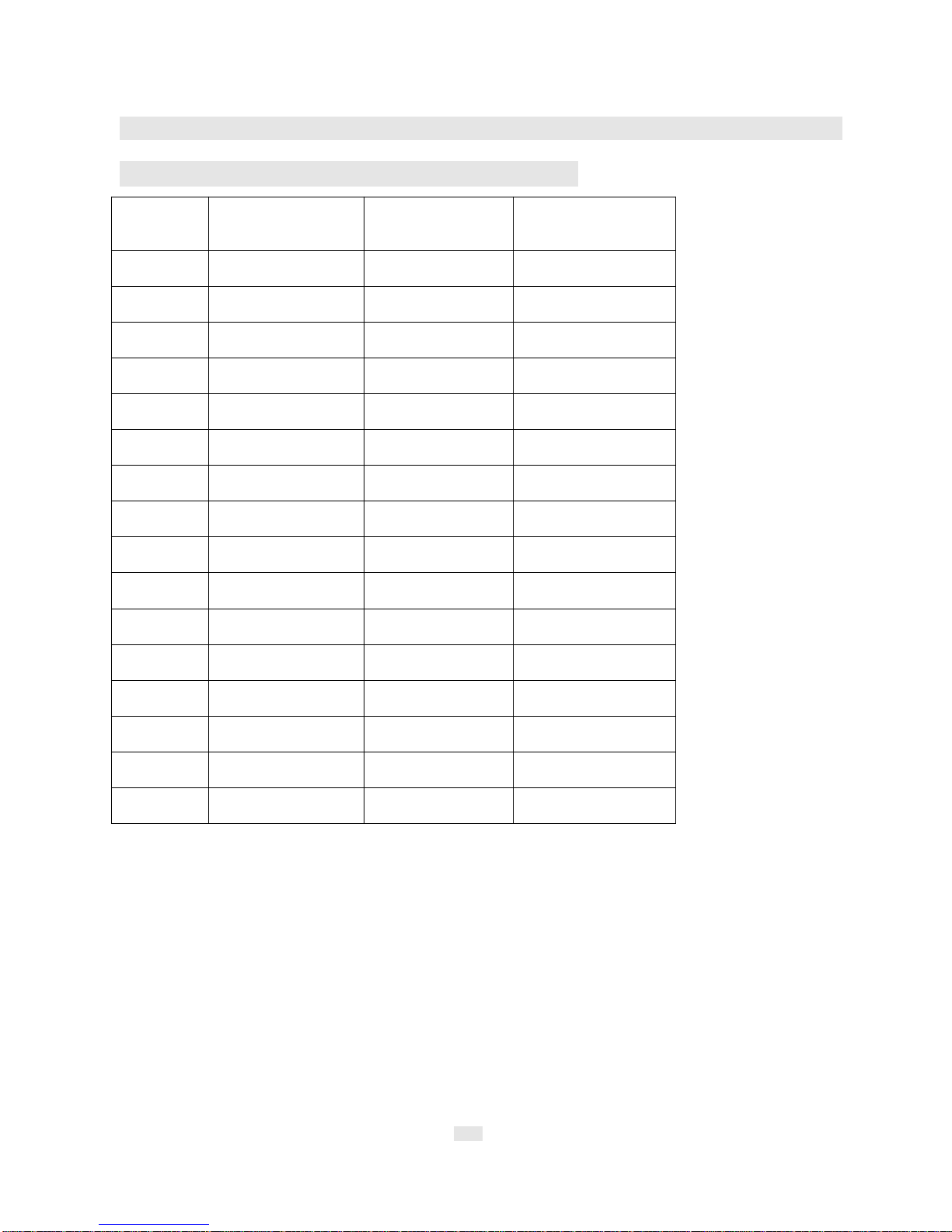
FACTORYDEFAULT SETTING
FC-301/D UHF Default Frequency and Tx Power
Channel RX Frequency TX
Frequency
TX Power
1 400.1250MHZ 400.1250MHZ 5W
2 405.1250MHZ 405.1250MHZ 5W
3 410.1250MHZ 410.1250MHZ 5W
4 415.1250MHZ 415.1250MHZ 5W
5 420.1250MHZ 420.1250MHZ 5W
6 425.1250MHZ 425.1250MHZ 5W
7 430.1250MHZ 430.1250MHZ 5W
8 435.1250MHZ 435.1250MHZ 5W
9 436.1250MHZ 436.1250MHZ 5W
10 440.1250MHZ 440.1250MHZ 5W
11 445.1250MHZ 445.1250MHZ 5W
12 450.125MHZ 450.1250MHZ 5W
13 455.1250MHZ 455.1250MHZ 5W
14 460.1250MHZ 460.1250MHZ 5W
15 465.1250MHZ 465.1250MHZ 5W
16 469.9750MHZ 469.9750MHZ 5W
 Loading...