

19-0009; Rev 2; 8/95
EVALUATION KIT MANUAL
FOLLOWS DATA SHEET
±18-Bit ADC with Serial Interface
_______________General Description
The MAX132 is a CMOS, 18-bit plus sign, serial-output,
analog-to-digital converter (ADC). Multi-slope integration provides high-resolution conversions in less time
than standard integrating ADCs, allowing operation up
to 100 conversions per second. Low conversion noise
provides guaranteed operation with ±512mV full-scale
input range (2µV/LSB). A simple 4-wire serial interface
connects easily to all common microprocessors, and
twos-complement output coding simplifies bipolar measurements. Typical supply current is only 60µA and is
reduced to 1µA in sleep mode. Four serially programmed digital outputs can be used to control an
external multiplexer or programmable-gain amplifier.
The MAX132 comes in 24-pin narrow DIP and wide SO
packages, and is available in commercial and extended temperature grades.
High resolution, compact size, and low power make this
device ideal for data loggers, weigh scales, data-acquisition systems, and panel meters.
________________________Applications
Remote Data Acquisition
Battery-Powered Instruments
Industrial Process Control
Transducer-Signal Measurement
Pressure, Flow, Temperature, Voltage
Current, Resistance, Weight
____________________________Features
♦ Low Supply Current:
60µA (Normal Operation)
1µA (Sleep-Mode Operation)
♦ ±0.006% FSR Accuracy at 16 Conv/sec
♦ Low Noise: 15µV
RMS
♦ Serial I/O Interface with Programmed Output for
Mux and PGA
♦ Performs up to 100 Conv/sec
♦ ±2pA Input Current
♦ 50Hz/60Hz Rejection
______________Ordering Information
PART
MAX132CNG
MAX132CWG
MAX132C/D 0°C to +70°C
MAX132ENG
MAX132EWG
MAX132MRG -55°C to +125°C
* Contact factory for dice specifications.
** Contact factory for availability and processing to MIL-STD-883.
TEMP. RANGE PIN-PACKAGE
0°C to +70°C
0°C to +70°C
-40°C to +85°C 24 Narrow Plastic DIP
-40°C to +85°C
24 Narrow Plastic DIP
24 Wide SO
Dice*
24 Wide SO
24 Narrow CERDIP**
MAX132
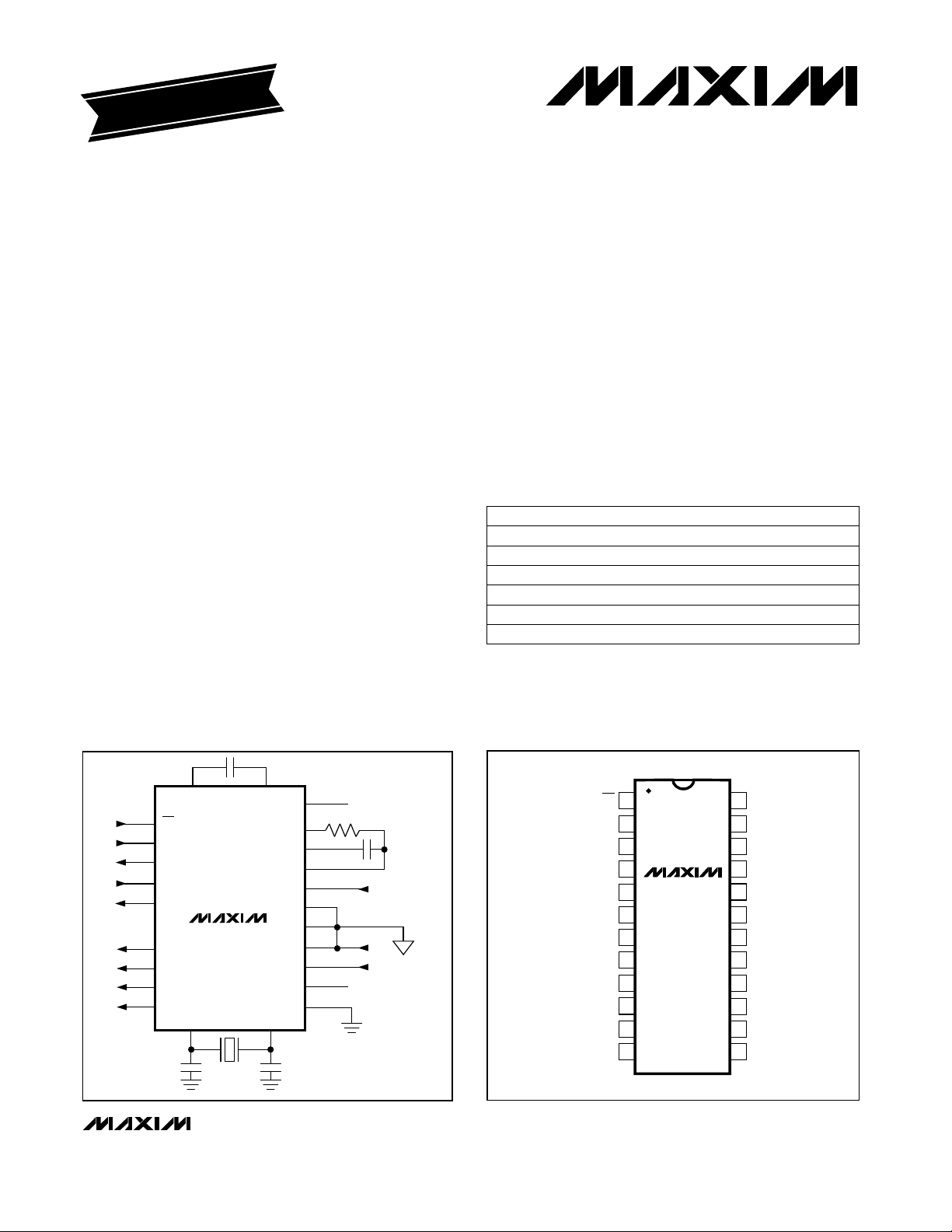
________________Functional Diagram
CREF- CREF+
CS
SCLK
EOC
DIN
DOUT
MAX132
P0
P1
P2
P3
________________________________________________________________
V+
BUF OUT
INT OUT
INT IN
REF+
REF-
AGND
IN LO
IN HI
V-
DGND
OSC2OSC1
+5V
602k
4.7nF
±512mV INPUT
-5V
__________________Pin Configuration
TOP VIEW
CS
1
DIN
2
DOUT
3
SCLK
4
OSC2
OSC1
P0
P1
P2
P3
EOC
DGND
MAX132
5
6
7
8
9
10
11
12
DIP/SO
Maxim Integrated Products
Call toll free 1-800-998-8800 for free samples or literature.
24
23
22
21
20
19
18
17
16
15
14
13
V+
BUF OUT
INT OUT
INT IN
CREFCREF+
REF+
REFAGND
IN LO
IN HI
V-
1

±18-Bit ADC with Serial Interface
ABSOLUTE MAXIMUM RATINGS
Supply Voltage
V+ to DGND..............................................-0.3V < V+ < +6.0V
V- to DGND ................................................+0.3V < V- < -9.0V
V+ to V-............................................................................+15V
Analog Input Voltage (any input).....................................V+ to V-
Digital Input Voltage .....................(DGND - 0.3V) to (V+ + 0.3V)
Continuous Power Dissipation
MAX132
Narrow Plastic DIP (derate 8.70mW/°C above +70°C)....478mW
Stresses beyond those listed under “Absolute Maximum Ratings” may cause permanent damage to the device. These are stress ratings only, and functional
operation of the device at these or any other conditions beyond those indicated in the operational sections of the specifications is not implied. Exposure to
absolute maximum rating conditions for extended periods may affect device reliability.
ELECTRICAL CHARACTERISTICS
(V+ = 5V, V- = -5V, DGND = AGND = IN LO = REF- = 0V, REF+ = 545mV, R
f
= 32,768Hz, 60Hz mode, TA= T
CLK
ACCURACY
Zero Error
Rollover Error
Conversion Time
Input Voltage Range
Leakage Current IN HI, IN LO
Common-Mode Rejection Ratio IN HI = IN LO
Common-Mode Range
Zero-Reading Drift
POWER REQUIREMENTS
Negative Supply Voltage
Positive Supply Rejection
Negative Supply Rejection
Negative Supply Current
Positive Sleep-Mode Current
Digital Ground Sleep-Mode
Current
to T
MIN
(Note 1)
VINHI = 0V % of FSR
(Notes 2, 3)
(Note 4)
f
= 32.768Hz
CLK
IN HI to IN LO, for specified accuracy
IN HI = IN LO V±3.0
(Note 3) ppm/°C±0.15 ±1.5
(Note 3) ppm/°C±5Scale Factor Temp. Coefficient
VINHI = 400mV, V- = -5.0V,
4.5V ≤ V+ ≤ 5.5V
VINHI = 400mV, V- = 5.0V,
-5.5V ≤ V- ≤ -4.5V
Digital input = 0V or V+
Digital input = 0V or V+
Digital input = 0V or V+
Digital input = 0V or V+
Digital input = 0V or V+ µA-1 -10Negative Sleep-Mode Current
Digital input = 0V or V+ µA0±2
, unless otherwise noted.)
MAX
CONDITIONS
Wide SO (derate 11.76mW/°C above +70°C)..............647mW
Narrow CERDIP (derate 12.50mW/°C above +70°C) ..688mW
Operating Temperature Ranges
MAX132C_ _ .......................................................0°C to +70°C
MAX132E_ _ ....................................................-40°C to +85°C
MAX132MRG.................................................-55°C to +125°C
Storage Temperature Range.............................-65°C to +160°C
Lead Temperature (soldering, 10sec).............................+300°C
TA= +25°C
TA= T
TA= +25°C
TA= +25°C
TA= T
TA= T
VCM= ±3.0V
TA= +25°C
TA= +25°C
TA= T
TA= +25°C
TA= T
MIN
MIN
MIN
MIN
MIN
to T
to T
to T
to T
to T
INT
MAX
MAX
MAX
MAX
MAX
= 602kΩ, C
= 0.0047µF, C
INT
±18Resolution
0 ±0.0076
±0.0168
0 ±0.010
±0.032
±2 ±10TA= +25°C
±12 ±250
±0.009 ±0.032VCM= ±500mV
±0.25 ±0.50
±0.003 ±0.0061
±0.003 ±0.0168
±0.003 ±0.0061
±0.003 ±0.0168
REF
% of FSR±0.0015 ±0.006Integral Nonlinearity
% of FSR
% of FSR
% of FSR±3.1Read-Zero 50Hz/60Hz Range
% of FSR
% of FSR
= 0.1µF,
UNITSMIN TYP MAXPARAMETER
Bits
ms63
mV±512
pA
µV15RMS Noise
V4.5 5.5Positive Supply Voltage
V-5.5 -4.5
µA60 125Positive Supply Current
µA-35 -65
µA-25 -60Digital Ground Supply Current
µA110
2 _______________________________________________________________________________________
±18-Bit ADC with Serial Interface
ELECTRICAL CHARACTERISTICS (continued)
(V+ = 5V, V- = -5V, DGND = AGND = IN LO = REF- = 0V, REF+ = 545mV, R
f
= 32,768Hz, 60Hz mode, TA= T
CLK
MIN
to T
, unless otherwise noted.)
MAX
CONDITIONS
DIGITAL SECTION
Output High
Output Low
Input High
Input Low
Input Current
Input Capacitance
DOUT, I
OH
DOUT, I
V
EOC, P0–P3, I
V
DOUT, I
OL
EOC, P0–P3, I
Referred to DGND, 4.5V ≤ V+ ≤ 5.5V, CS, DIN, SCLK
IH
Referred to DGND, 4.5V ≤ V+ ≤ 5.5V, CS, DIN, SCLK
IL
CS, DIN, SCLK, and DOUT when three-stated
IN
CS, DIN, SCLK, and DOUT when three-stated
IN
OUT
OUT
OUT
= -1mA
= -100µA
= -100µA
OUT
= 1.6mA
= 100µA
OUT
= 602kΩ, C
INT
= 0.0047µF, C
INT
3.5 4.3
4.0 4.5
4.0 4.7
0.1 0.4
0.1 0.4
INTERFACE TIMING
(Test Circuit of Figure 1, Figure 2, V+ = 5V, V- = -5V, DGND = AGND = 0V, TA= +25°C, unless otherwise noted.) (Note 3)
CONDITIONS
CS Lead Time
CS Lag Time
S
High Time
CLK
S
Low Time
CLK
CS High Pulse Width
DIN to SCLK Setup Time
DIN to SCLK Hold Time
DOUT Access Time from Three-State
Data Valid
DOUT Disable Time to Three-State
Delay to P0–P3 High
Delay to P0–P3 Low
1
2
3
4
5
6
7
8
9
10
11
12
See Figure 3
See Figure 4
REF
MAX132
= 0.1µF,
UNITSMIN TYP MAXSYMBOLPARAMETER
V
V
V2.4V
V0.8V
nA±10 ±500I
pF5C
UNITSMIN TYP MAXSYMBOLPARAMETER
ns500t
ns400t
ns400t
ns300t
µs1t
ns0t
ns200t
ns320t
ns60t
ns320t
ns230 350t
ns230 350t
Note 1: ±18-bit accuracy achieved by averaging multiple conversions.
Note 2: Maximum deviation from best straight-line fit.
Note 3: Guaranteed by design, not tested.
Note 4: Difference in reading for equal positive and negative inputs near full scale.
_______________________________________________________________________________________ 3
±18-Bit ADC with Serial Interface
__________________________________________Typical Operating Characteristics
ERROR vs. COMMON-MODE
INPUT VOLTAGE (V
0.05
IN HI = IN LO
0
-0.05
MAX132
-0.10
-0.15
ERROR (% OF FSR)
-0.20
-0.25
-0.30
-3 -2 -1 0 1 2 3 4-4
COMMON-MODE VOLTAGE (V)
vs. CRYSTAL FREQUENCY
140
120
100
80
60
40
20
SUPPLY CURRENT (µA)
0
-20
-40
0 50 150
100 200 250 300 350
CRYSTAL FREQUENCY (kHz)
LO–AGND)
IN
SUPPLY CURRENT
50Hz/60Hz READ-ZERO OFFSET
vs. VREF
4.5
MAX132-01
4.0
3.5
3.0
2.5
2.0
1.5
1.0
READ-ZERO OFFSET (% OF FSR)
0.5
0
50Hz MODE
0 0.5 1.5
60Hz MODE
1.0 2.0
VREF (V)
MAX132-02
READ-ZERO OFFSET (% OF FSR)
FULL-SCALE ROLLOVER ERROR
vs. VREF
0.10
V+
V-
MAX132-04
0.08
0.06
0.04
0.02
ROLLOVER ERROR (% OF FSA)
0
0 0.5 1.0 1.5 2.52.0
VREF (V)
MAX132-05
)
RMS
NOISE (µV
50Hz/60Hz READ-ZERO OFFSET
vs. TEMPERATURE
1.6
1.4
1.2
1.0
0.8
0.6
0.4
0.2
0
-40 -20 20
60Hz MODE, VREF = 545mV
50Hz MODE, VREF = 655mV
0 40 60 80 100
TEMPERATURE (°C)
NOISE vs. NUMBER
OF SAMPLES AVERAGED
20
15
10
5
0
0102030 5040
NUMBER OF SAMPLES AVERAGED
MAX132-03
MAX132-06
______________________________________________________________Pin Description
PIN
CHIP SELECT Input has 3 functions: 1) When low, selects IC for communication; 2) on rising edge, loads
CS1
input shift register data into one of the command registers; 3) on falling edge, loads data from one of the
output registers into the output shift register. When CS is high, DOUT is high impedance.
Serial Data In, D7 first bit in. Data is clocked into the register on the rising edge of SCLK.DIN2
Serial Data Out, D7 first bit out. Data is clocked out at the falling edge of SCLK. High impedance when CSis high.DOUT3
SCLK4
Serial Clock Input. On SCLK’s rising edge, data is shifted into the internal shift register through DIN. On
SCLK’s falling edge, data is clocked out of DOUT.
Oscillator Output 2 is normally connected to a 32,768Hz crystal. Do not connect with external clock source.OSC25
Oscillator Input 1 is normally connected to a 32,768Hz crystal, or may be connected to an external clock.OSC16
User-programmable output bit 0—programmed through the serial port.P07
User-programmable output bit 1—programmed through the serial port.P18
4 _______________________________________________________________________________________
FUNCTIONNAME

±18-Bit ADC with Serial Interface
_________________________________________________Pin Description (continued)
PIN
User-programmable output bit 2—programmed through the serial port.P29
User-programmable output bit 3—programmed through the serial port.P310
End of Conversion Output goes high at end of conversion.EOC11
Digital Ground—power-supply returnDGND12
Negative Supply, nominally -5VV-13
Positive Analog InputIN HI14
Negative Analog InputIN LO15
Analog GroundAGND16
Negative Reference InputREF-17
Positive Reference InputREF+18
Positive Reference Capacitor connectionCREF+19
Negative Reference Capacitor connectionCREF-20
Integrator Input. Connect the integration capacitor between INT IN and INT OUT.INT IN21
Integrator Output. To minimize noise, this pin should drive the capacitor’s outside foil (negative end).INT OUT22
Buffer-Amplifier Output drives the integrator resistor.BUF OUT23
Positive Supply, nominally +5VV+24
FUNCTIONNAME
MAX132
1
CS
4
SCLK
11
EOC
2
DIN
3
DOUT
7
P0
8
P1
9
P2
10
P3
32,768Hz
15pF
Figure 1. Test and Typical Application Circuit
REF+
REF-
IN LO
IN HI
15pF
+5V
24
V+
602k
23
22
4.7nF
21
18
17
16
15
14
13
V-
-5V
12
0.1µF
20
CREF- CREF+
MAX132
65
19
BUF OUT
INT OUT
INT IN
AGND
DGND
OSC2OSC1
120k
100k
40.2k
512mV INPUT
2.5V
MAX872
_______________________________________________________________________________________ 5
±18-Bit ADC with Serial Interface
____________Functional Description
The MAX132 integrates the input voltage for a fixed
period of time, then deintegrates a known reference
voltage and measures the time required to reach zero.
Good line rejection is achieved by setting the (input)
integration time equal to one 50Hz or 60Hz period. The
MAX132 has a 50Hz/60Hz mode selection bit that sets
MAX132
the integration time to 655/545 clock periods, respectively, so that 50Hz/60Hz rejection is obtained with a
32,768Hz crystal. The MAX132 is tested and guaranteed at a 16 conv/sec throughput rate. Figure 1 shows
the basic MAX132 application circuit, with component
values selected for 16 conv/sec .
For applications that don’t require 50Hz/60Hz rejection,
the MAX132 will operate up to 100 conv/sec at reduced
accuracy (typically 0.012% FSR nonlinearity, or ±13
bits). In these applications, the 50Hz mode is recommended because of its longer (655 count) integration
time. See
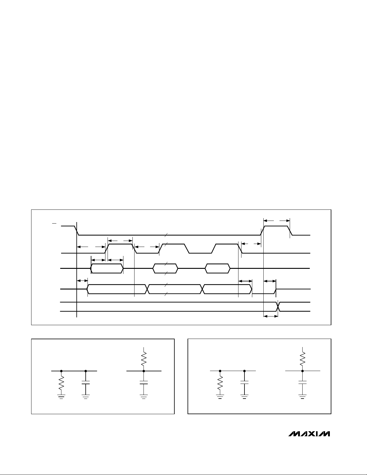
Increased Speed
CS
SCLK
t
1
section.
t
6
t
3
t
7
t
4
__________Analog Design Procedure
Input Voltage Range
and Input Protection
The recommended analog full-scale input range is
±512mV. Performance is tested and guaranteed at
±512mV full scale, corresponding to a 2µV/LSB resolution at 18 bits. Resolution is defined as follows:
Re / ( ) / ,solution Volts LSB V FS
[]
which corresponds to 2µV/LSB resolution at 18 bits.
Consult the
Typical Operating Characteristics
vs. Number of Samples Averaged and other important
operating parameters. Note how accuracy depends on
common-mode input voltage (common mode is defined
here as |VINLO - AGND|). For optimum performance,
set the analog input full-scale between ±470mV and
= 262144
IN
t
5
t
2
for Noise
DIN
DOUT
P0–P3
t
8
MSB IN B6–B1 LSB IN
t
9
LSB OUTB6–B1MSB OUT
t
t11, t
10
12
Figure 2. Serial-Mode Timing
+5V
3k
DOUT DOUT
3k
DGND DGND
a. High-Z to VOH (t8) b. High-Z to VOL (t8)
C
L
C
L
Figure 3. Load Circuits for Access Time
6 _______________________________________________________________________________________
DOUT DOUT
3k
DGND DGND
a. VOH to High-Z (t10) b. VOL to High-Z (t10)
10pF
Figure 4. Load Circuits for Disable Time to Three-State
+5V
3k
10pF

±18-Bit ADC with Serial Interface
±660mV for 60Hz mode operation or between ±390mV
and ±550mV for 50Hz mode operation. The pseudodifferential input voltage is applied across pins 14 and
15 (IN HI, IN LO), and can range to within 2V of either
supply rail.
The inputs IN HI and IN LO lead directly to CMOS transistor gates, yielding extremely high input impedances
that are useful when converting signals from a high
input source impedance, such as a sensor. Input currents are only 2pA typical at +25°C. Figure 6 shows an
RC filter at the input to optimize noise performance.
Fault protection is accomplished by the 100kΩ series
resistance. Internal protection diodes, which clamp the
analog inputs from V+ to V-, allow the channel input
pins to swing from (V- - 0.3V) to (V+ + 0.3V) without
damage. However, if the analog input voltage at the
pins IN HI or IN LO exceed the supplies, limit the current into the device to less than 1mA, as excessive current will damage the device.
Reference Voltage Selection
The reference voltage sets the analog input voltage
range. For the nominal ±512mV full-scale input range, a
545mV reference voltage is used for the 60Hz mode
and a 655mV reference voltage is used in the 50Hz mode.
The reference voltage can be calculated as follows:
60
Hz Mode V
:
REF
( ) () )
=
262144
,
IN FS
()
545 512
counts V
or
50
Hz Mode V
:
REF
( ) () )
=
262144
,
IN FS
()
655 512
counts V
The recommended reference voltage range is 500mV
to 700mV. The MAX132 is tested with the nominal
545mV reference voltage in 60Hz mode. Use amplifiers
or attenuators (resistor dividers) to scale other full-scale
input signal ranges to the recommended ±512mV fullscale range.
References outside the recommended range may be
used with a degradation of linearity. A reference voltage from 200mV to 500mV will result in a lower signalto-noise ratio; a reference voltage from 700mV to 2V will
increase the rollover error.
The MAX872 2.50V reference, with its 10µA supply current, is ideally suited for the MAX132. Figure 7 shows
how 2.50V can be divided to obtain the desired reference voltage. The reference input accepts voltages
anywhere within the converter’s power-supply range;
however, for best performance, neither REF+ nor REFshould come within 2V of the supplies.
MAX132
C
DE-
DE+
REF
DE+
DE-
INT
REF+CREF+
DE DE
INT
IN HI
AGND
INT
IN LO
Figure 5. Analog Section Block Diagram
_______________________________________________________________________________________ 7
R
REF- CREF- INT IN INT OUT
REST
BUFFER
BUFFER
INT
C
INT
INTEGRATOR
8pF
64pF
MAX132
X8
COMPARATOR 1
Z1+ x 8
TO
DIGITAL
SECTION
COMPARATOR 2

±18-Bit ADC with Serial Interface
Differential Reference Inputs
and Rollover Error
The main source of rollover voltage error is due to
common-mode voltages. This error is caused by the
reference capacitor losing or gaining charge to stray
capacitance. A positive signal with a large commonmode voltage can cause the reference capacitor to
gain charge (increase voltage). In contrast, the refer-
MAX132
ence capacitor will lose charge (decrease voltage)
when deintegrating a negative input signal. Rollover
error is a direct result of the difference in reference to
positive or negative input voltages. With the recommended reference capacitor types, the worst-case
rollover error is 0.01% of full-scale. Connect REF- to
AGND to minimize rollover error. As outlined in the reference section, reference voltages below 500mV also
contribute to rollover errors.
+5V
24
V+
MAX132
V-
-5V
+545mV
18
REF+
13
±512mV
100k
0.1µF
14
IN HI
15
IN LO
16
AGND
17
REF-
Oscillator Circuit
The internal oscillator is typically driven by a crystal, as
shown in Figure 8, or by an external clock. If an external clock is used, connect the clock to OSC1 and leave
OSC2 floating. The duty-cycle can vary from 20% to
80%. The typical threshold voltage is approximately 2V.
For proper start-up, a full +5V CMOS-logic swing is
required.
The oscillator frequency sets the conversion rate. Use
32,768Hz for applications that require 50Hz or 60Hz
line rejection. This frequency yields 16 conv/sec. The
same clock frequency can be used to reject both line
frequencies because the MAX132 integrates for a different number of clock cycles in its 50Hz and 60Hz
modes. In each case, the MAX132 integrates for a single complete line cycle (20ms for the 50Hz mode,
16.67ms for the 60Hz mode). Refer to the
Speed
section for operation at higher conversion rates.
Increased
External Components
The MAX132 requires an integrator resistor (R
capacitor (C
), a reference capacitor (C
INT
crystal. All MAX132 tests are performed with a
32,768Hz crystal frequency. The crystal frequency, reference voltage, and integrator current determine the
values of R
INT
and C
INT
.
REF
) and
INT
), and a
Crystal
Figure 8 shows the internal oscillator drive circuitry used
with external crystals. The two external capacitors provide
DC bias at start-up. The 15pF capacitors shown are typical
values. The actual capacitance will vary, depending on the
crystal manufacturer’s recommendation and board layout.
Figure 6. MAX132 Input Circuit
+5V
1M
120k
REF+
1µF
REF-
Figure 7. Dividing MAX872 to Generate the MAX132’s
Reference Voltage
8 _______________________________________________________________________________________
100k
40.2k
MAX872
2.5V
150k
OSC1 OSC2
65
Figure 8. MAX132 Internal Oscillator Drive Circuitry
5pF5pF
15pF15pF
+5V
MAX132
±18-Bit ADC with Serial Interface
Table 1. Crystal Frequencies and
Integrator Capacitors for 50Hz to 60Hz
Operation
Crystal
Conv/sec
16
32
48
64
80
96
Note: Capacitor values are for a 3.0V integrator swing.
Manufactures of miniature quartz resonators include:
Freq.
(Hz)
32,768
65,536
98, 304
131,072
163,840
196,608
Epson of America
C-2 (through-hole), MC-306 (SMD)
Phone: (310) 787-6300; Fax: (310) 782-5320
The integrator resistor sets the maximum integrator output current for the integrate phase. A 602kΩ low-noise,
metal-film integrator resistor is recommended for use
with reference voltages between 545mV and 655mV.
Best linearity is achieved when the integration current
(I
) does not exceed 2.5µA. For other reference volt-
INT
ages, select R
INT
=
R
INT
and
=
I
INT
The oscillator frequency, integrator resistor, and integrator capacitor set the maximum integrator output voltage swing for full-scale reading. The integrator voltage
swing is about 3V and should not come within 2V of
either supply rail to avoid saturation. A 602kΩ integrator
resistor and a 4.7nF integrator capacitor are recommended with a clock frequency of 32,768Hz. If different
clock frequencies are used, select C
lowing equations:
C
INT
(pF)
4700
2700
1800
1200
1000
/60Hz
820
C
INT
(pF)
6800
3300
2000
1500
1200
1000
/50Hz
Resistor
(kΩ)
602
602
602
602
602
602
Integrator Resistor
as follows:
V
REF
25 05µµ
V
R
<<
. .
AI A
INT
REF
INT
Integrator Capacitor
using the fol-
INT
t
INT
545
, mod
=
f
for Hz e
OSC
60
or
t
INT
655
, mod
=
f
for Hz e
OSC
50
The integrator capacitor’s dielectric absorption directly
affects integral nonlinearity. High-quality metal-film
capacitors are recommended in the following order of
preference: polypropylene, polystyrene, polycarbonate, and polyester (Mylar). The polyester capacitor will
generate some integral nonlinearity.
To minimize noise, INT OUT should drive the outside
foil (negative end) of the capacitor. Manufacturers of
polypropylene capacitors include Sprague (715P),
Panasonic (ECQ-P), Roderstein (KP1835), Wima (FKP),
and CSF Thompson (PL/PS).
Reference Capacitor
The reference capacitor must be small enough to fully
charge from a discharged state on power-up in reasonable time, and large enough so the charge does not
droop excessively during a conversion. The reference
capacitor is normally 0.1µF for all oscillator frequencies.
For applications that require a physically smaller capacitor, the equation below will maintain C
.=0 0033
f
OSC
C
REF
proportionality:
REF
The reference capacitor must have low leakage, since
it stores the reference voltage while floating during the
deintegrate phase. Any leakage or charge loss during
this phase changes the scale factor and will cause an
error. Appropriate metal-film capacitors recommended
for their low-leakage characteristics1are (in this order):
polypropylene (up to +105°C, large size), teflon (suitable for use up to +125°C, large size), polystyrene,
polycarbonate, and polyester.
At temperatures above +85°C, capacitor leakage may
affect accuracy. In such cases, increasing the value of
C
up to 50% and more will help at the expense of
REF
longer start-up time at power-on. The start-up time is
proportional to C
tCFxxk
START UP REF−
and can be estimated by:
REF
= () µ 10 100 Ω
MAX132
Vt
() ()
IN FS INT
C
=<<135
INT
()
RV
() ( )
INT SWING
where V V V
, . ;
SWING
and
_______________________________________________________________________________________ 9
1
Pease, R.A., “Understanding Capacitor Soakage to Optimize
EDN
Analog Systems,”
, October 13, 1982, p.125.

±18-Bit ADC with Serial Interface
___________________Digital Interface
Serial data at DIN is sent in 8-bit packets and is shifted
into the internal 8-bit shift register with each rising edge
of SCLK. The data is then latched into either command
input register 0 or command input register 1, as determined by the LSB of the data sent, and is latched on
the rising edge of CHIP SELECT (CS) Data is clocked
MAX132
out of the selected output register on each falling edge
of SCLK. D7(MSB) must be the first data bit to be shifted in and is the first bit to be shifted out.
Output data is shifted out at the same time command
data is shifted in. Command data must be clocked in
on the previous 8-bit read-write cycle to receive conversion data in the present cycle.
Since there is no internal power-on reset, initialize the
MAX132 immediately after power-up to insure correct
operation.
Table 2 defines each bit of five registers: the two command input registers, output register 0, output register
1, and the status output register.
Command Input Register 0
Register-Set Bits
Data bits D1 and D2 of command register 0 (RS1 and
RS0) determine the data to be read on the data bus.
These bits select which register outputs data to the bus.
Table 3 defines the bit values that determine which register is read on the next cycle (Figure 9).
REGISTER
INSTRUCTION
(DATA IN)
OUTPUT DATA
Figure 9. Instruction and Data Sequencing
CYCLE 1
START,
READ STATUS
CYCLE 2
READ HIGHER
BITS
OUTPUT STATUS
REGISTER
(EOC, POLARITY, B2–B0)
CYCLE 3
READ LOWER
BITS
REGISTER 1
( B11–B18)
CYCLE 4
START,
READ STATUS
REGISTER 0
( B3–B10)
Read-Zero Bit
The read-zero bit allows the ADC to calibrate on command for zero offset. The read-zero bit, when set to 1,
internally shorts the inputs; when a start-conversion
command is given, the zero error is converted. Subtract
the results from the standard external measurement
conversion when the read-zero conversion ends. If the
read-zero bit is set to 0, the converter measures the
voltage between IN Hl and IN LO once a start bit is
given. Take a new zero reading periodically and whenever the ambient temperature, the reference voltage, or
the common-mode input voltage are changed.
Table 3. Register Set-Bit Definitions
RS1
RS0
0
0
Selects Register 0; output for data bits B3–B10
0
1
Selects Register 1; output for data bits B11–B18
Selects Register 2; output status for data bits
1
0
B0–B2, polarity, sleep, integrating, EOC, and
collision bit
1 1 Invalid data
DEFINITIONS
Table 2. Register Map of Input and Output Data
REGISTER
Command Input
Register 0
Command Input
Register 1
Output Register 0
RS1 = 0, RS0 = 0
Output Register 1
RS1 = 0, RS0 = 1
Output Status
Register
RS1 = 1, RS0 = 0
*Note: Refer to Table 3.
10 ______________________________________________________________________________________
“1”
“0”
“1”
“0” No Collision Converting
D7 D6 D5 D4 D3 D2 D1 D0
Start
Convert
Returns to
0 at EOC
Set P3
Output
B10
B18
MSB
Collision
50Hz
60Hz
Set P2
Output
B9
B17
EOC
Sleep
Awake
Set P1
Output
B8
B16
Integrating
Input
Not
Integrating
DATA BIT
Read Zero
Read V
Set P0
Output
B7
B15
Sleep
Awake +Polarity
IN
Don’t Care
Don’t Care
Don’t Care
B14
-Polarity
B6
RS0*
Don’t Care
B5
B13
B2 B1
Don’t Care
RS1*
B4
B12
0
1
B3
B11
B0
LSB

±18-Bit ADC with Serial Interface
Averaging 2 or 3 read-zero measurements provides the
most accurate read-zero value. Perform a read-zero
sequence whenever a large change in the input voltage
is expected.
Sleep Bit
When the sleep bit is set to 1, (bit D5 in command input
register 0), the low-power sleep mode starts when EOC
returns high. In sleep mode, the supply current is typically 1µA and the oscillator shuts down. The interface
remains active and data can be read. When exiting
sleep mode, the analog circuitry needs time to stabilize
before the next conversion starts. Accomplish this by
writing a dummy instruction to emerge from sleep
mode, and wait at least one conversion cycle before
writing a start instruction.
50Hz/60Hz
With a 32,768Hz crystal, the 50Hz/60Hz bit sets the
integrate period equal to one line cycle for 50Hz/60Hz
environments. When D6 (in command input register 0)
is set to 0, the integrate count is an integer multiple of
60Hz (32,768Hz/60Hz = 546 counts). When D6 is set to
1, the integrate input count is an integer multiple of
50Hz (32,768Hz/50Hz = 655 counts). Achieve the
greatest AC rejection by adjusting the integration period for 50Hz or 60Hz.
Start Conversion Bit
The start conversion bit (D7) in command input register
0 initiates a conversion when set to 1. The MAX132
immediately starts a conversion, stops at conversion
end, and then waits for the next start-bit command. A
start instruction is needed to initiate each conversion.
To initiate a continuous data stream, write a separate
start command for each conversion in three ways:
1) Wait longer than a known conversion time and then
write another start command.
2) Poll either the EOC status register bit or the EOC
line to determine conversion end and start time for
the next conversion. EOC becomes 1 at conversion
end at count 0000 of the conversion counter (Figure
10).
3) Set the start bit to 1 before a conversion end. The
internal conversion counter is then checked for its
count. If the count is 0000 (EOC = 1), a new conversion starts and the conversion counter is set to
0001. The start bit resets to 0 after 5 clock cycles.
The MAX132 will not check the start bit again until
the conversion counter returns to a 0000 count. This
means a start command can be given any time after
0005 internal conversion count; the next conversion
starts when the counter returns to 0000.
MAX132
RESET 60Hz
0000
Figure 10. Conversion Timing (Negative Input Shown)
INT START
0001
ZERO INT
INT OUT
INTERNAL CONVERSION DATA LATCH
0111
INTEGRATE
50Hz mode
655
60Hz mode
______________________________________________________________________________________ 11
545
CHOP
659 667
DE-1 DE-2 DE-3 DE-4X8-1 X8-2 X8-3 ZERO INT
679
MAX
545
MAX
SOFT
OVERRANGE
AREA
(SEE TEXT)
47
RESET EVENTS
30
LATCH
16001346 1638 1783 1823 1970 2017 2047 0000
264
38 145
40 147
EOC
±18-Bit ADC with Serial Interface
Table 4. Overrange Values for
Resolution Used
Bits
Used
B18–B3
B18–B2
MAX132
B18–B1
B18–B0 ±18
Resolution
Bits
±15
±16
±17
Soft Overrange
Start Value
34,880
69,760
139,520
279,040 350,440
Hard Overrange
Maximum Value
43,805
87,610
175,220
Table 5. Output Values for 16-Bit
Resolution (Offset Corrected)
Input
+640mV
+576mV
+545mV
+512mV
+448mV
+384mV
+320mV
+256mV +4000 +16384
+192mV
+128mV
+64mV +1000 +4096
+15µV
0 +0000 0
-15µV
-64mV
-128mV
-192mV -D000 -12288
-256mV
-320mV
-384mV
-448mV -9000 -28672
-512mV
-545mV
-576mV
-640mV
* Soft Overrange Operation
Note: The MAX132 exhibits additional errors when operating
in the soft overrange area. Operation in this region is not
included in the specifications. The soft overrange values listed
in Table 5 do not include error correction.
Hexadecimal
Reading
+A000
+9000
+8840
+8000
+7000
+6000
+5000
+3000
+2000
+0001
-FFFF
-F000
-E000
-C000
-B000
-A000
-8000
-77C0
-7000
-6000
Decimal
Counts
+40960*
+36864*
+34880*
+32768 Positive Full Scale
+28672
+24576
+20480
+12288
+8192
+1
-1
-4096
-8192
-16384
-20480
-24576
-32768
-34880*
-36864*
-40960*
Comment
Positive Reference
Voltage
Negative Full Scale
Negative Reference
Voltage
Command Input Register 1
User-Programmable Output Bits P0 to P3
Command input register 1 always has data bit D0 = 1.
Data bits D4 to D7 of command register 1 control the
states of the user-programmable output pins P0 to P3,
respectively (Table 2). These four outputs can be used
to control an external multiplexer, programmable gain
amplifier, or other devices.
Output Registers
Output data is the sum of system offset (read zero) plus
the results of the external input voltage measurement.
Register 0
Register 0 contains the low-byte (bits B3–B10) conversion data. New data is available after EOC goes high.
Access register 0 by setting RS0 and RS1 to 0.
Register 1
Register 1 contains the high-byte (bits B11–B18) data.
Data is in a twos-complement format‚ where the polarity
bit is a 1 for negative polarity data. Access register 1
by setting control bits RS0 = 1 and RS1 = 0 when writing to the command input register.
Status Register
Bits B0–B2
The B0, B1, and B2 bits are located in the status register. At the end of each conversion these bits are updated and read back from the status register. For full
18-bit resolution, use bits B0–B2. Average multiple
results to increase accuracy. The polarity bit information is necessary to determine if the reading is not in
overrange (Tables 4 and 5).
Integrate Bit
The integrate (INT) bit is set to 1 at the beginning of the
integration phase and becomes 0 at the end. Poll INT
to determine the earliest time the input can be changed
without affecting the conversion.
End-of-Conversion Bit
The end-of-conversion (EOC) bit signals conversion status. If EOC is 1, the conversion is complete and the ADC
waits in zero-integrate mode at time = 0000 for the next
start instruction. A conversion cycle has 2048 counts.
EOC becomes 1 at count 0000 and 0 at count 0001.
Collision Bit
The collision bit warns the microprocessor (µP) that the
register’s data was changed during the read cycle. A
collision occurs if the internal result latches on the falling
edge of CS, causing the collision bit to be set to 1 on the
rising edge of the next CS. This occurs because these
two pulses are asynchronous. Once the status register is
12 ______________________________________________________________________________________

±18-Bit ADC with Serial Interface
read, the collision bit is automatically reset to 0. To determine collision status, read the status register collision bit
before and after reading output registers 0 and 1.
Collisions will not occur if a conversion’s read cycle is
completed before the next conversion begins.
Sequence Counter and Results Counter
A binary sequencing counter controls the conversion
phase’s sequencing (or timing). In integrate phase,
both start and stop occur at preset counts. The deintegration phases start at predetermined counts, but are
terminated when the comparator detects zero crossing
at the integrator output.
The results counter accumulates counts during all deintegrate phases. It is an up/down binary counter, with
the count direction determined by the deintegration
polarity. In the first deintegrate phase, the results
counter counts by 512. Since the second deintegrate
phase deintegrates a residual voltage multiplied by 8,
the results counter increments or decrements by 64
during this phase. It increments or decrements by 8
during the third deintegrate phase, and by 1 during the
fourth deintegrate phase. The results counter content
transfers to the results register at each conversion end.
Overrange Indication
B18 is not strictly an overrange bit. This 19th bit is necessary to exploit the converter’s full range, and to
ensure that a full 18-bit result can be achieved after a
zero reading has been deducted.
The actual overrange value is a function of the number
of bits of resolution used. Table 4 lists the overrange
values for different resolutions.
The MAX132 has two overrange levels (Figure 10 and
Table 4). The first level is a soft overrange that is set by
the user. Overrange is arbitrarily set at a value, preferably less than the 279,040 (including any zero offset)
raw counts soft limit. A nonlinearity step of about 64
counts occurs at raw count 279,040 and again at
330,240 counts.
The second level is a hard overrange with a maximum
value of 350,440 counts. Attempts to deintegrate values
greater than this will result in a value of ±350,440 counts.
____Multislope Conversion Phases
Multislope conversion allows 350,440 counts with a clock
frequency of only 32.768kHz. After zero-crossing, the
main comparator (with some delay) sends a signal to the
digital control section, which then terminates the deintegrate period by issuing commands to the analog switches. This action entails further delay because the
commands must be synchronous with the clock. As a
result, the delay between zero-crossing and switch actuation can exceed one clock cycle. A “residue” voltage
that represents unwanted extra counts in the conversion
result is left on the capacitor, while the integrator’s output
continues past the zero crossing.
Dual-slope converters ignore this residue voltage error.
However, the multislope MAX132 inverts, amplifies, and
deintegrates the residue, canceling the extra counts by
driving an up/down counter in the opposite direction.
This process of measuring and accounting for the residue
can be repeated for the successively smaller errors
remaining after each deintegration. (Deintegration is simply an integration of V
grator output ramps toward zero.) The MAX132, for
example, executes three cycles in which the residue is
inverted, multiplied by eight, and deintegrated (Figure 10).
, with polarity chosen so the inte-
REF
Integrate Phase
The MAX132 integrates the input signal by connecting
the integrator’s noninverting input to IN LO, and the
buffer input to IN Hl. The integration period is 545
counts for 60Hz mode and 655 counts for 50Hz
Deintegrate Phase
The integrator capacitor’s voltage polarity at the end of
integrate phase determines the polarity of the first deintegration phase. The first deintegration phase ends
when the comparator detects that the integration
capacitor has been discharged. The MAX132 then
goes into a rest phase, where both the buffer input and
the integrator’s noninverting input are connected to
AGND, integrating the system offset.
Near the end of the maximum allowable deintegration
period, the integrator capacitor voltage polarity is again
sampled, resulting in either a positive or negative deintegrate cycle.
Rest Phase
A rest phase follows each deintegrate phase. The rest
phase starts when the integrator crosses zero and ends
when the maximum count for that deintegration phase
has been reached.
First Times-Eight Phase
When the zero crossing is detected at the end of the
deintegrate phase, deintegration continues until the
next clock cycle. This causes the integrator to overshoot zero crossing slightly, leaving a small residual
voltage on the integration capacitor. The first timeseight (X8) phase inverts and multiplies this residual by
a factor of 8.
MAX132
______________________________________________________________________________________ 13

±18-Bit ADC with Serial Interface
Second Deintegrate Phase
The second deintegrate phase deintegrates residual
voltage on the integration capacitor that has been
through the X8 phase. Since the voltage across the
integration capacitor has been multiplied by 8, each
deintegration clock cycle corresponds to 1/8 of one
clock cycle during the first deintegration.
MAX132
Additional Times-Eight
and Deintegrate Phases
At the end of the second and third deintegration phases, the device performs a X8 multiplication of the residual voltage left on the integration capacitor. After each
of these X8 multiplications, a deintegration occurs,
resulting in a second, third, and fourth deintegration
phase. Each time the residual voltage on the integration
capacitor is multiplied by 8, the following deintegration
has 8 times finer resolution.
Zero-Integrate Phase
The zero-integrate phase zeros out the integrator to
prepare for the next integration (Figure 10). This phase
occurs at the beginning and end of each conversion. At
power-up, or in the hold mode prior to a conversion, the
MAX132 continues to zero integrate until a conversion
starts. When a conversion starts in 60Hz mode, another
111 clocks of zero integrate are completed before the
beginning of a conversion. In 50Hz mode, only one
additional zero integrate is performed before the conversion starts. An additional 20 clocks of zero integrate
occur at each conversion end.
__________Applications Information
Extended Delays Between Conversions
An extended delay between conversions can degrade
the subsequent conversion result due to capacitor
droop and internal offset/common-mode voltages. The
initial reading may be off by 4 to 6 counts in a ±15-bit
configuration. When the delay between conversions
exceeds 2 seconds (either because of a slower conversion rate or the use of sleep mode), it is recommended
that the first reading after this delay be discarded.
Increased Speed
The MAX132 is tested with a 32,768Hz clock frequency, which results in 16 conv/sec. Up to 96 conv/sec
may be achieved with higher clock frequencies and
some changes in component values, as shown in Table
1. Operation at higher conversion rates reduces accuracy, and care must be taken to get the best results.
Although either the 50Hz or 60Hz mode can be used,
complete rejection of 50Hz or 60Hz normal-mode noise
at conversion rates above 16 conv/sec is impossible.
Use the 50Hz mode when operating at more than 16
conv/sec, irrespective of the local line frequency. The
50Hz mode uses a slightly longer integration time than
the 60Hz mode, and generally gives lower-noise performance.
Table 1 lists the crystal frequencies and integrating
capacitor values for the 50Hz and 60Hz modes for various conversion rates, although the 50Hz mode is recommended for clock rates above 32,768Hz.
The raw data can be used where highest accuracy is
not required, and the least significant bits can be
ignored. At 96 conv/sec, the accuracy is 13 bits.
Improvements in accuracy can be gained by averaging
both the data and the zero readings, although data
averaging compromises the converter’s speed performance.
To maximize throughput, take zero readings only when
necessary, i.e., when the common-mode voltage
changes. It is not normally necessary to take a zero reading after every data reading‚ as an excessive number of
zero readings reduces the converter’s effective speed.
Noise Reduction
To minimize noise, each supply must be bypassed to
GND with a 0.1µF capacitor. A ground plane should
also be placed under the analog circuitry. Use the RC
network at the inputs as shown in Figure 6. Also refer to
the section “Noise Reduction Techniques” in the notes
for the MAX132 evaluation kit. To minimize the coupling
effects of stray capacitance, keep digital lines as far
from analog components and lines as possible. Also,
connect the integrator capacitor’s outside foil to the INT
OUT pin to minimize stray capacitive coupling. If possible, keep the digital interface inactive while the
MAX132 is converting.
Ratiometric Measurements
Figure 11 shows an application to measure temperature ratiometrically with an RTD sensor. The voltage
drops across the RTD sensor and the 250Ω reference
resistor are generated by the same current source. The
voltage of the sensor (VS) is fed directly into the differential inputs, and the voltage drop across the reference
resistor (VR) is brought into the differential reference
inputs. The relationship of these voltages is ratiometric
and unaffected by the actual current. The MAX132’s
output is proportional to VSdivided by VR, independent
14 ______________________________________________________________________________________
±18-Bit ADC with Serial Interface
of the overall accuracy of the current source. The current source delivers 2mA, resulting in about 500mV
across the 250Ω resistor—suitable to fit the MAX132’s
±512mV full-scale range. Note that the accuracy of the
reference resistor (0.1%) sets the circuit’s accuracy.
The power consumption of the RTD sensor is small
(0.5mW), minimizing errors caused by self-heating.
Interfacing to a µP Parallel Port
Figure 12 shows a high-level software subroutine for
reading output/status data and writing command data
+5V
0.1µF10µF
DATA IN
DATA OUT
CLOCK
RTD
PT100
IN
IC1
MAX872
GND
V
S
OUT
RW1
4.096V
V
R
INTERFACE
2k
250Ω
0.1%
SERIAL-
DATA
CHIP SELECT
to the MAX132. It provides an algorithm for serial communication when the µP port does not have a predefined serial interface protocol (i.e., SPI™ or Microwire™).
The routine sends command data (TxByte) to the
MAX132 while concurrently collecting the MAX132’s
output register data (selected by the previous write
cycle). Note that a write is required before each read to
change the next output register to be read, and that
the subroutine must be repeated three times to read
the output status register, Output Register 0, and
Output Register 1.
-5V +5V
0.1µF
600k
4.7nF
0.1µF
32,768Hz
13
V- V+
1
CS
2
DIN
3
DOUT
4
SCLK
11
EOC
7
PG0
8
PG1
9
PG2
10
PG3
14
IN HI
15
IN LO
DGND
12 16
IC2
MAX132
AGND
10µF
24
BUF OUT
INT OUT
INT IN
CREF+
CREF-
REF+ IN
REF- IN
OSC2
OSC1
23
22
21
19
20
18
17
5
6
MAX132
RW2
Figure 11. Ratiometric Configuration Using the Differential Reference Inputs
SPI is a trademark of Motorola, Inc. Microwire is a trademark of National Semiconductor Corp.
______________________________________________________________________________________ 15
RW1, RW2 WIRE RESISTANCE
±18-Bit ADC with Serial Interface
___________________Chip Topography
WAIT UNTIL EOC PIN IS HIGH
CLEAR SCLK
CLEAR CS
SCLK
DOUT
DINCSV+
BUF OUT
INT OUT
MAX132
WRITE DIN132 FROM TxByte’s MSB
READ DOUT132 INTO RxByte’s LSB
SET SCLK
CLEAR SCLK
SHIFT RxByte LEFT
SHIFT TxByte LEFT
REPEAT 8 TIMES
SET CS
RETURN RxByte
OSC2
OSC1
PG0
PG1
PG2
PG3
EOC
DGND
0.144"
(3.66mm)
IN HI
V- IN LO
INT IN
CREF-
CREF+
0.186"
(4.72mm)
REF+
REF-
AGND
Figure 12. MAX132 Read/Write Algorithm
16 ______________________________________________________________________________________
TRANSISTOR COUNT: 2799
SUBSTRATE CONNECTED TO V+
 Loading...