

AVAILABLE
For pricing, delivery, and
ordering information, please contact Maxim Direct
at 1-888-629-4642, or visit Maxim’s website at www.maximintegrated.com.
General Description
The DS24B33 is a 4096-bit, 1-Wire® EEPROM organized as 16 memory pages of 256 bits each. Data is
written to a 32-byte scratchpad, verified, and then
copied to the EEPROM memory. The DS24B33 communicates over a single-conductor 1-Wire bus. The communication follows the standard 1-Wire protocol. Each
device has its own unalterable and unique 64-bit registration number that is factory programmed into the chip.
The registration number is used to address the device
in a multidrop 1-Wire net environment. The DS24B33 is
software compatible to the DS2433.
Applications
Storage of Calibration Constants
Board Identification
Storage of Product Revision Status
Features
o 4096 Bits of Nonvolatile EEPROM Partitioned Into
Sixteen 256-Bit Pages
o Read and Write Access is Highly Backward-
Compatible to the DS2433
o 256-Bit Scratchpad with Strict Read/Write
Protocols Ensures Integrity of Data Transfer
o Unique, Factory-Programmed, 64-Bit Registration
Number Ensures Error-Free Device Selection and
Absolute Part Identity
o Switchpoint Hysteresis to Optimize Performance
in the Presence of Noise
o Communicates to Host at 15.4kbps or 125kbps
Using 1-Wire Protocol
o Low-Cost Through-Hole and SMD Packages
o Operating Range: +2.8V to +5.25V, -40°C to +85°C
o IEC 1000-4-2 Level 4 ESD Protection (±8kV
Contact, ±15kV Air, Typical) for IO Pin
1-Wire 4Kb EEPROM
Ordering Information
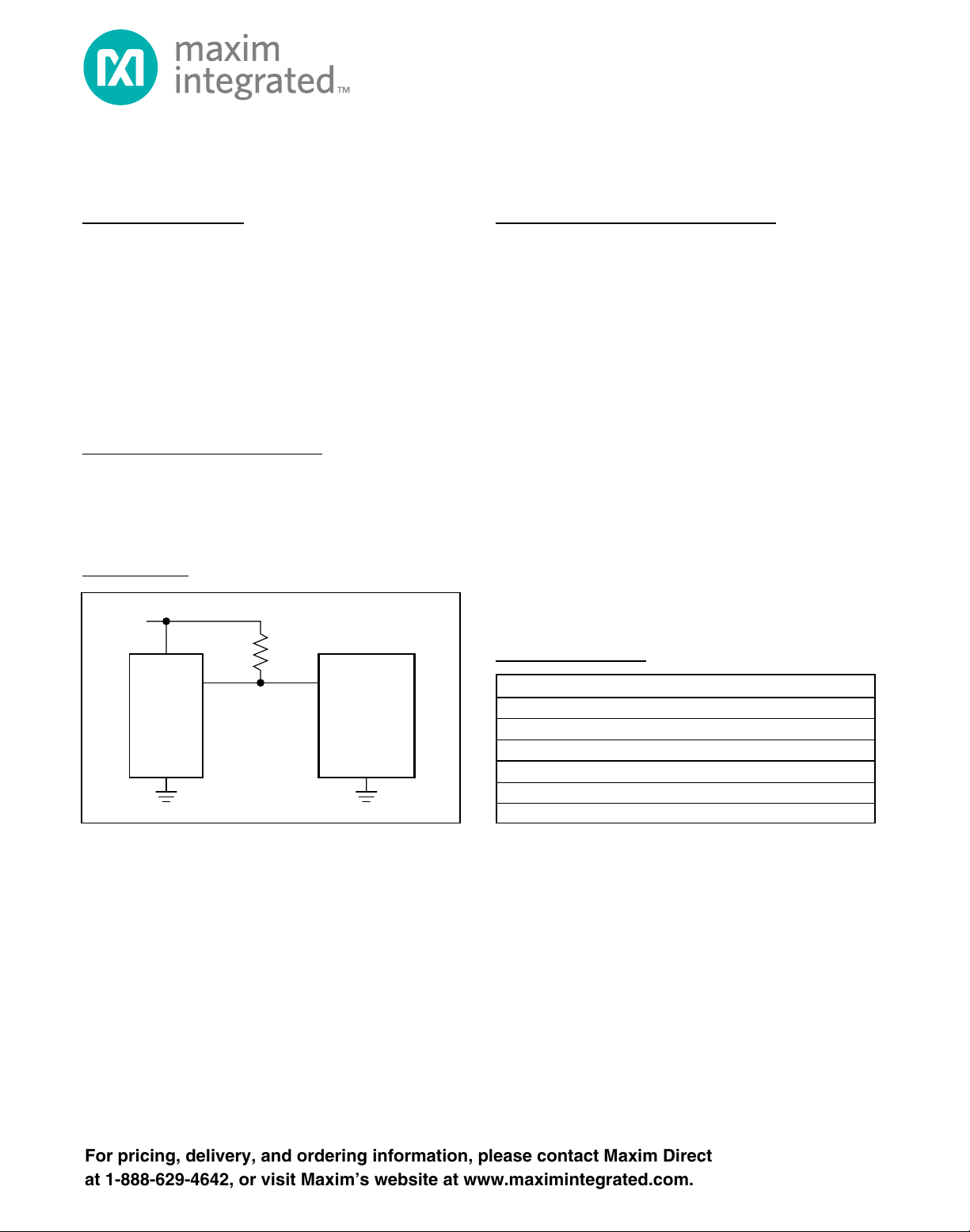
IO
R
PUP
V
CC
µC
GND
DS24B33
Typical Operating Circuit
Note: The leads of TO-92 packages on tape and reel are formed
to approximately 100-mil (2.54mm) spacing. For details, refer to
the package outline drawing.
+
Denotes a lead(Pb)-free/RoHS-compliant package.
T&R = Tape and reel.
*EP = Exposed pad.
PART TEMP RANGE PIN-PACKAGE
DS24B33+ -40°C to +85°C TO-92
DS24B33+T&R -40°C to +85°C TO-92
DS24B33G+T&R -40° C to +85°C 2 SFN (2.5k pcs)
DS24B33Q+T&R -40° C to +85°C 6 TDFN-EP* (2.5k pcs)
DS24B33S+ -40°C to +85°C 8 SO (208 mil s)
DS24B33S+T&R -40°C to +85°C 8 SO (208 mi ls)
1-Wire is a registered trademark of Maxim Integrated Products, Inc.
19-5759; Rev 3; 5/12
DS24B33

1-Wire 4Kb EEPROM
ABSOLUTE MAXIMUM RATINGS
ELECTRICAL CHARACTERISTICS
(TA= -40°C to +85°C.) (Note 1)
Stresses beyond those listed under “Absolute Maximum Ratings” may cause permanent damage to the device. These are stress ratings only, and functional
operation of the device at these or any other conditions beyond those indicated in the operational sections of the specifications is not implied. Exposure to
absolute maximum rating conditions for extended periods may affect device reliability.
IO Voltage Range to GND ........................................-0.5V to +6V
IO Sink Current....................................................................20mA
Operating Temperature Range ...........................-40°C to +85°C
Junction Temperature......................................................+150°C
Storage Temperature Range .............................-55°C to +125°C
Lead Temperature (soldering, 10s) .................................+300°C
Soldering Temperature (reflow)
TO-92 ...........................................................................+250°C
All other packages, excluding SFN .............................+260°C
2
Maxim Integrated
DS24B33
PARAMETER S YMBOL CONDITIONS MIN TYP MAX UNITS
IO PIN: GENERAL DATA
1-Wire Pullup Voltage V
1-Wire Pullup Resistance R
Input Capacitance CIO (Notes 5, 6) 2000 pF
Input Load Current I
High-to-Low Switching Threshold V
Input Low Voltage V
Low-to-High Switching Threshold V
Switching Hysteresis V
Output Low Voltage V
Recovery Time
(Notes 2, 13)
Time-Slot Duration
(Notes 2, 14)
IO PIN: 1-Wire RESET, PRES ENCE-DETECT CYCLE
Reset Low Time
(Note 2)
Presence-Detect High Time t
Presence-Detect Low Time t
Presence-Detect Samp le Time
(Notes 2, 15)
(Notes 2, 3) 2.8 5.25 V
PUP
PUP
t
REC
t
SLOT
t
RSTL
PDH
PDL
t
MSP
(Notes 2, 4) 0.3 2.2 k
IO at V
L
TL
IL
TH
HY
OL
PUPMAX
(Notes 6, 7, 8) 0.5
(Notes 2, 9) 0.5 V
(Notes 6, 7, 10) 1.0
(Notes 6, 7, 11) 0.2 1.7 V
At 4mA (Note 12) 0.4 V
Standard speed 5
Overdrive speed 2
V
+4.5V 1
PUP
Directl y prior to reset pulse 640µs 5
Directl y prior to reset pulse > 640µs 10
Standard speed 65
Standard speed, V
Overdrive speed 8
Overdrive speed, V
Standard speed, t
Standard speed, t
Overdrive speed 48 80
Standard speed 15 60
Overdrive speed 2 6
Standard speed 60 240
Overdrive speed 8 24
Standard speed 60 75
Overdrive speed 6 10
0.05 5 µA
-
V
PUP
1.8
V
PUP
1.0
+4.5V 61
PUP
+4.5V 7
PUP
before reset = 10µ s 480 960
REC
before reset = 5µs 480 640
REC
V
V
µs
µs
µs
µs
µs
µs

1-Wire 4Kb EEPROM
ELECTRICAL CHARACTERISTICS (continued)
(TA= -40°C to +85°C.) (Note 1)
Note 1: Limits are 100% production tested at TA= +25°C and/or TA= +85°C. Limits over the operating temperature range and
relevant supply voltage range are guaranteed by design and characterization. Typical values are not guaranteed.
Note 2: System requirement.
Note 3: When operating near the minimum operating voltage (2.8V), a falling edge slew rate of 15V/µs or faster is recommended.
Note 4: Maximum allowable pullup resistance is a function of the number of 1-Wire devices in the system, 1-Wire recovery times,
and current requirements during EEPROM programming. The specified value here applies to systems with only one
device and with the minimum 1-Wire recovery times. For more heavily loaded systems, an active pullup such as that found
in the DS2482-x00 or DS2480B may be required.
Note 5: Capacitance on the data pin could be 2500pF when V
PUP
is first applied. Once the parasite capacitance is charged, it
does not affect normal communication.
Note 6: Guaranteed by design, characterization, and/or simulation only. Not production tested.
Note 7: V
TL
, VTH, and VHYare a function of the internal supply voltage, which is a function of V
PUP
, R
PUP
, 1-Wire timing, and
capacitive loading on IO. Lower V
PUP
, higher R
PUP
, shorter t
REC
, and heavier capacitive loading all lead to lower values of
VTL, VTH, and VHY.
Note 8: Voltage below which, during a falling edge on IO, a logic 0 is detected.
Note 9: The voltage on IO must be less than or equal to V
ILMAX
at all times while the master is driving IO to a logic 0 level.
Note 10: Voltage above which, during a rising edge on IO, a logic 1 is detected.
Note 11: After V
TH
is crossed during a rising edge on IO, the voltage on IO must drop by at least VHYto be detected as logic 0.
Note 12: The I-V characteristic is linear for voltages less than +1V.
Note 13: Applies to a single DS24B33 attached to a 1-Wire line.
Note 14: Defines maximum possible bit rate. Equal to 1/(t
W0LMIN
+ t
RECMIN
).
Note 15: Interval after t
RSTL
during which a bus master can read a logic 0 on IO if there is a DS24B33 present. The power-up presence
detect pulse could be outside this interval but will be complete within 2ms after power-up.
Note 16: ε in Figure 11 represents the time required for the pullup circuitry to pull the voltage on IO up from V
IL
to VTH. The actual
maximum duration for the master to pull the line low is t
W1LMAX
+ tF- ε and t
W0LMAX
+ tF- ε, respectively.
Note 17: δ in Figure 11 represents the time required for the pullup circuitry to pull the voltage on IO up from V
IL
to the input high
threshold of the bus master. The actual maximum duration for the master to pull the line low is t
RLMAX
+ tF.
Note 18: Current drawn from IO during the EEPROM programming interval. The pullup circuit on IO should be such that during the
programming interval, the voltage at IO is greater than or equal to V
PUPMIN
. If V
PUP
in the system is close to V
PUPMIN
, then
a low-impedance bypass of R
PUP
, which can be activated during programming, may need to be added.
Maxim Integrated
3
DS24B33
PARAMETER S YMBOL CONDITIONS MIN TYP MAX UNITS
IO PIN: 1-Wire WRITE
Write-Zero Low Time
(Notes 2, 16)
Write-One Low Time
(Notes 2, 16)
t
W0L
t
W1L
IO PIN: 1-Wire READ
Read Low Time
(Notes 2, 17)
Read Sample Time
(Notes 2, 17)
t
RL
t
MSR
EEPROM
Programm ing Current I
Programm ing T ime t
Write/Erase C yc les (Endurance)
(Notes 20, 21)
PROG
PROG
N
Data Retention (Notes 22, 23, 24) tDR At +85°C (worst case) 40 Years
Standard speed 60 120
Overdrive speed 6 16
Standard speed 5 15
Overdrive speed 1 2
Standard speed 5 15 -
Overdrive speed 1 2 -
Standard speed tRL + 15
Overdrive speed tRL + 2
(Note 18) 2 mA
(Note 19) 5 m s
At +25°C 200,000
CY
At +85°C (worst case) 50,000
µs
µs
µs
µs
—

ELECTRICAL CHARACTERISTICS (continued)
(TA= -40°C to +85°C.) (Note 1)
Note 19: The t
PROG
interval begins after the trailing rising edge on IO for the last time slot of the E/S byte for a valid copy scratchpad sequence. The interval ends once the device’s self-timed EEPROM programming cycle is complete and the current
drawn by the device has returned from I
PROG
to IL.
Note 20: Write-cycle endurance is degraded as T
A
increases.
Note 21: Not 100% production tested; guaranteed by reliability monitor sampling.
Note 22: Data retention is degraded as T
A
increases.
Note 23: Guaranteed by 100% production test at elevated temperature for a shorter time; equivalence of this production test to data
sheet limit at operating temperature range is established by reliability testing.
Note 24: EEPROM writes can become nonfunctional after the data-retention time is exceeded. Long-time storage at elevated tem-
peratures is not recommended; the device can lose its write capability after 10 years at +125°C or 40 years at +85°C.
1-Wire 4Kb EEPROM
Pin Configurations
4
Maxim Integrated
DS24B33
N.C.
N.C.
IO
GND
TOP VIEW
1
2
3
4
TOP VIEW
+
DS24B33
SO
(208 mils)
DS24B33
+
16N.C. N.C.
25IO N.C.
34GND N.C.
*EP
24B33
ymrrF
8
7
6
5
N.C.
N.C.
N.C.
N.C.
GND
IO
N.C.
TO-92
FRONT VIEWSIDE VIEW
1
2
3
FRONT VIEW (T&R VERSION)
1
2
3
1
2
3
BOTTOM VIEW
12
DS24B33
IO GND
(6mm × 6mm × 0.9mm)
SFN
*EXPOSED PAD
(3mm
TDFN
× 3mm)
NOTE: THE SFN PACKAGE IS QUALIFIED FOR ELECTRO-MECHANICAL CONTACT
APPLICATIONS ONLY, NOT FOR SOLDERING. FOR MORE INFORMATION, REFER TO
APPLICATION NOTE 4132: ATTACHMENT METHODS FOR ELECTRO-MECHANICAL
SFN PACKAGE.
Detailed Description
The DS24B33 combines 4Kb of data EEPROM with a
fully featured 1-Wire interface in a single chip. The
memory is organized as 16 pages of 256 bits each. A
volatile 256-bit memory page called the scratchpad
acts as a buffer when writing data to the EEPROM to
ensure data integrity. Data is first written to the scratchpad, from which it can be read back for verification
before transferring it to the EEPROM. The operation of
the DS24B33 is controlled over the single-conductor
1-Wire bus. Device communication follows the standard
1-Wire protocol. The energy required to read and write
the DS24B33 is derived entirely from the 1-Wire communication line. Each DS24B33 has its own unalterable
and unique 64-bit registration number. The registration
number guarantees unique identification and is used to
address the device in a multidrop 1-Wire net environment. Multiple DS24B33 devices can reside on a common 1-Wire bus and be operated independently of
each other. Applications of the DS24B33 include calibration data storage, PCB identification, and storage of
product revision status. The DS24B33 provides a high
degree of backward compatibility with the DS2433,
including having the same family code.
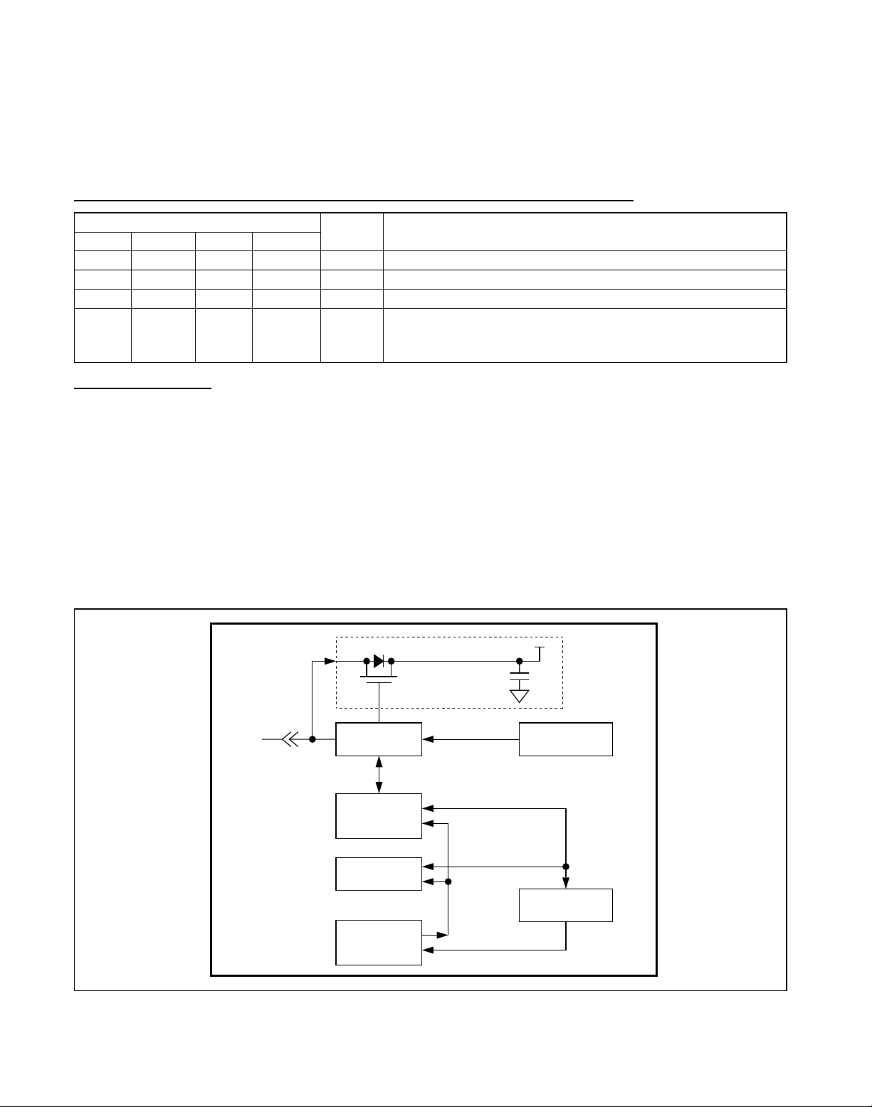
Overview
Figure 1 shows the relationships between the major
control and memory sections of the DS24B33. The
DS24B33 has four main data components: 64-bit
Pin Description
1-Wire 4Kb EEPROM
Figure 1. Block Diagram
Maxim Integrated
5
DS24B33
PIN
SFN TDFN-EP TO-92 SO NAME FUNCTION
2 3 1 4 GND Ground Reference
1 2 2 3 IO
— 1, 4, 5, 6 3 1, 2, 5–8 N.C. Not Connected
— — — — EP
1-Wire Bus Interface. Open-drain pin that requires external pullup
Exposed Pad (TDFN onl y). Solder evenly to the board’s ground plane for
proper operation. Refer to Application Note 3273: Exposed Pads: A Brief
Introduction for additional information.
1-Wire NET
1-Wire FUNCTION
CONTROL
PARASITE POWER
64-BIT REGISTRATION
NUMBER
DS24B33
MEMORY
FUNCTION
CONTROL UNIT
CRC-16
GENERATOR
32-BYTE
SCRATCHPAD
DATA MEMORY
16 PAGES OF
32 BYTES EACH

1-Wire 4Kb EEPROM
Figure 2. Hierarchical Structure for 1-Wire Protocol
MSB
8-BIT
CRC CODE
48-BIT SERIAL NUMBER
MSB MSBLSB
LSB
LSB
8-BIT FAMILY CODE
(23h)
MSBLSB
Figure 3. 64-Bit Registration Number
registration number, 32-byte scratchpad, sixteen
32-byte pages of EEPROM, and a CRC-16 generator.
Figure 2 shows the hierarchical structure of the
1-Wire protocol. The bus master must first provide
one of the seven ROM (network) function commands:
Read ROM, Match ROM, Search ROM, Skip ROM,
Resume, Overdrive-Skip ROM, or Overdrive-Match
ROM. Upon completion of an overdrive ROM command byte executed at standard speed, the device
enters overdrive mode where all subsequent communication occurs at a higher speed. Figure 9
describes the protocol required for these ROM function commands. After a ROM function command is
successfully executed, the memory functions
become accessible and the master can provide any
one of the four memory function commands. Figure 7
describes the protocol for these commands. All data
is read and written least significant bit (LSB) first.
Parasite Power
Figure 1 shows the parasite power supply. This circuitry
“steals” power whenever the IO input is high. IO provides sufficient power as long as the specified timing
and voltage requirements are met.
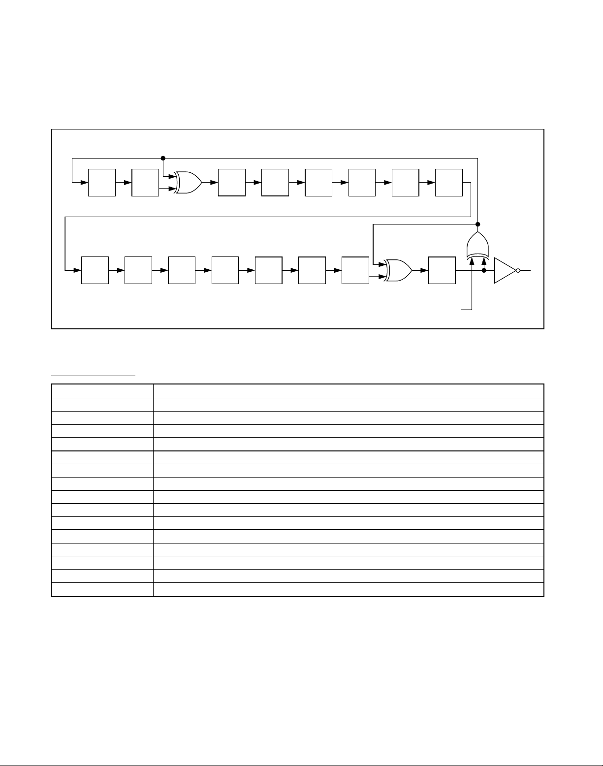
64-Bit Registration Number
Each DS24B33 contains a unique registration number
that is 64 bits long. The first 8 bits are a 1-Wire family
code. The next 48 bits are a unique serial number. The
last 8 bits are a cyclic redundancy check (CRC) of the
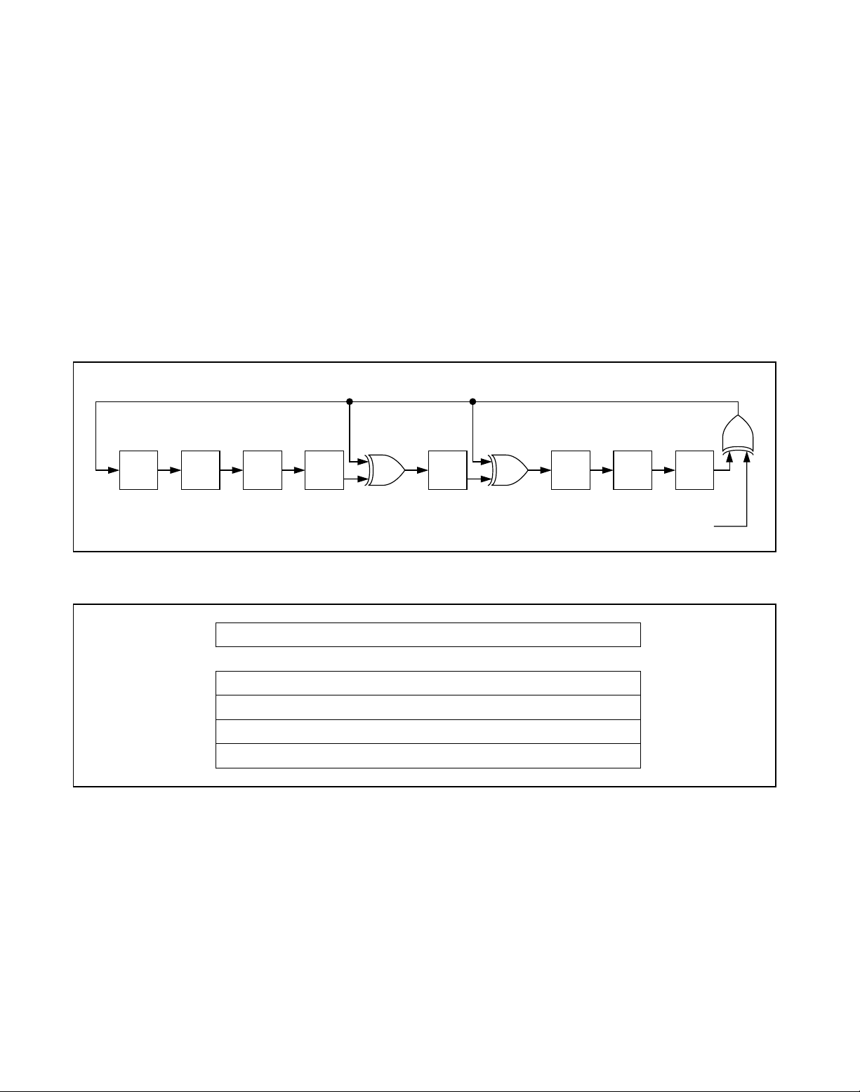
first 56 bits. See Figure 3 for details. The 1-Wire CRC is
generated using a polynomial generator consisting of a
shift register and XOR gates as shown in Figure 4. The
polynomial is X8 + X5 + X4 + 1. Additional information
about the 1-Wire CRC is available in Application Note
27:
Understanding and Using Cyclic Redundancy
Checks with Maxim iButton® Products
.
iButton is a registered trademark of Maxim Integrated Products, Inc.
6
Maxim Integrated
DS24B33
COMMAND LEVEL:
1-Wire ROM
FUNCTION COMMANDS
AVAILABLE COMMANDS: DATA FIELD AFFECTED:
READ ROM
MATCH ROM
SEARCH ROM
SKIP ROM
RESUME
OVERDRIVE-SKIP ROM
OVERDRIVE-MATCH ROM
DS24B33
64-BIT REG. #, RC-FLAG
64-BIT REG. #, RC-FLAG
64-BIT REG. #, RC-FLAG
RC-FLAG
RC-FLAG
RC-FLAG, OD-FLAG
64-BIT REG. #, RC-FLAG, OD-FLAG
DS24B33-SPECIFIC
MEMORY FUNCTION COMMANDS
WRITE SCRATCHPAD
READ SCRATCHPAD
COPY SCRATCHPAD
READ MEMORY
32-BYTE SCRATCHPAD, FLAGS
32-BYTE SCRATCHPAD
DATA MEMORY
DATA MEMORY
1-Wire 4Kb EEPROM
Figure 4. 1-Wire CRC Generator
32-BYTE INTERMEDIATE STORAGE SCRATCHPAD
ADDRESS
0000h to 001Fh 32-BYTE FINAL STORAGE EEPROM PAGE 0
0020h to 003Fh 32-BYTE FINAL STORAGE EEPROM PAGE 1
0040h to 01DFh FINAL STORAGE EEPROM PAGES 2 to 14
01E0h to 01FFh 32-BYTE FINAL STORAGE EPPROM PAGE 15
Figure 5. Memory Map
The shift register bits are initialized to 0. Then, starting
with the LSB of the family code, one bit at a time is
shifted in. After the 8th bit of the family code has been
entered, the serial number is entered. After the last bit
of the serial number has been entered, the shift register
contains the CRC value. Shifting in the 8 bits of the
CRC returns the shift register to all 0s.
Memory
The DS24B33 EEPROM array (Figure 5) consists of 16
pages of 32 bytes each, starting at address 0000h and
ending at address 01FFh. In addition to the EEPROM,
the device has a 32-byte volatile scratchpad. Writes to
the EEPROM array are a two-step process. First, data
is written to the scratchpad and then copied into the
main array. The user can verify the data in the scratchpad prior to copying.
Maxim Integrated
7
DS24B33
POLYNOMIAL = X8 + X5 + X4 + 1
1ST
STAGE
0
X
2ND
STAGE
1
X
3RD
STAGE
2
X
4TH
STAGE
3
X
5TH
STAGE
4
X
6TH
STAGE
5
X
7TH
STAGE
6
X
8TH
STAGE
7
X
INPUT DATA
8
X

1-Wire 4Kb EEPROM
Memory Access
Address Registers and Transfer Status
The DS24B33 employs three address registers: TA1,
TA2, and E/S (Figure 6). Registers TA1 and TA2 must
be loaded with the target address to which the data is
written or from which data is read. Register E/S is a
read-only transfer status register used to verify data
integrity with write commands. ES bits E[4:0] are
loaded with the incoming T[4:0] on a Write Scratchpad
command and increment on each subsequent data
byte. This is, in effect, a byte-ending offset counter
within the 32-byte scratchpad. Bit 5 of the E/S register,
called the partial byte flag (PF), is set if the number of
data bits sent by the master is not an integer multiple of
8 or if the data in the scratchpad is not valid due to a
loss of power. A valid write to the scratchpad clears the
PF bit. Bit 6 has no function; it always reads 0. The
highest valued bit of the E/S register, called authorization accepted (AA), is valid only if the PF flag reads 0. If
PF is 0 and AA is 1, the data stored in the scratchpad
has already been copied to the target memory address.
Writing data to the scratchpad clears this flag.
Writing with Verification
To write data to the DS24B33, the scratchpad must be
used as intermediate storage. First, the master issues
the Write Scratchpad command to specify the desired
target address, followed by the data to be written to the
scratchpad. Under certain conditions (see the
Write
Scratchpad [0Fh]
section) the master receives an
inverted CRC-16 of the command, address, and data at
the end of the Write Scratchpad command sequence.
Knowing this CRC value, the master can compare it to
the value it has calculated itself to decide if the communication was successful and proceed to the Copy
Scratchpad command. If the master could not receive
the CRC-16, it should send the Read Scratchpad command to verify data integrity. As a preamble to the
scratchpad data, the DS24B33 repeats the target
address TA1 and TA2 and sends the contents of the
E/S register. If the PF flag is set, data did not arrive correctly in the scratchpad or there was a loss of power
since data was last written to the scratchpad. The master does not need to continue reading; it can start a
new trial to write data to the scratchpad. Similarly, a set
AA flag together with a cleared PF flag indicates that
the device did not recognize the write command. If
everything went correctly, both flags are cleared and
the ending offset indicates the address of the last byte
written to the scratchpad. Now the master can continue
reading and verifying every data byte. After the master
has verified the data, it can send the Copy Scratchpad
command, for example. This command must be followed exactly by the data of the three address registers
TA1, TA2, and E/S. The master should obtain the contents of these registers by reading the scratchpad. As
soon as the DS24B33 has received these bytes correctly,
it starts copying the scratchpad data to the requested
location.
BIT NUMBER 7 6 5 4 3 2 1 0
TARGET ADDRESS (TA1) T7 T6 T5 T4 T3 T2 T1 T0
TARGET ADDRESS (TA2) T15 T14 T13 T12 T11 T10 T9 T8
ENDING ADD RESS WITH
DAT A STATUS (E/S)
(READ ONLY)
AA 0 PF E4 E3 E2 E1 E0
Figure 6. Address Registers
8
Maxim Integrated
DS24B33

1-Wire 4Kb EEPROM
Memory Function Commands
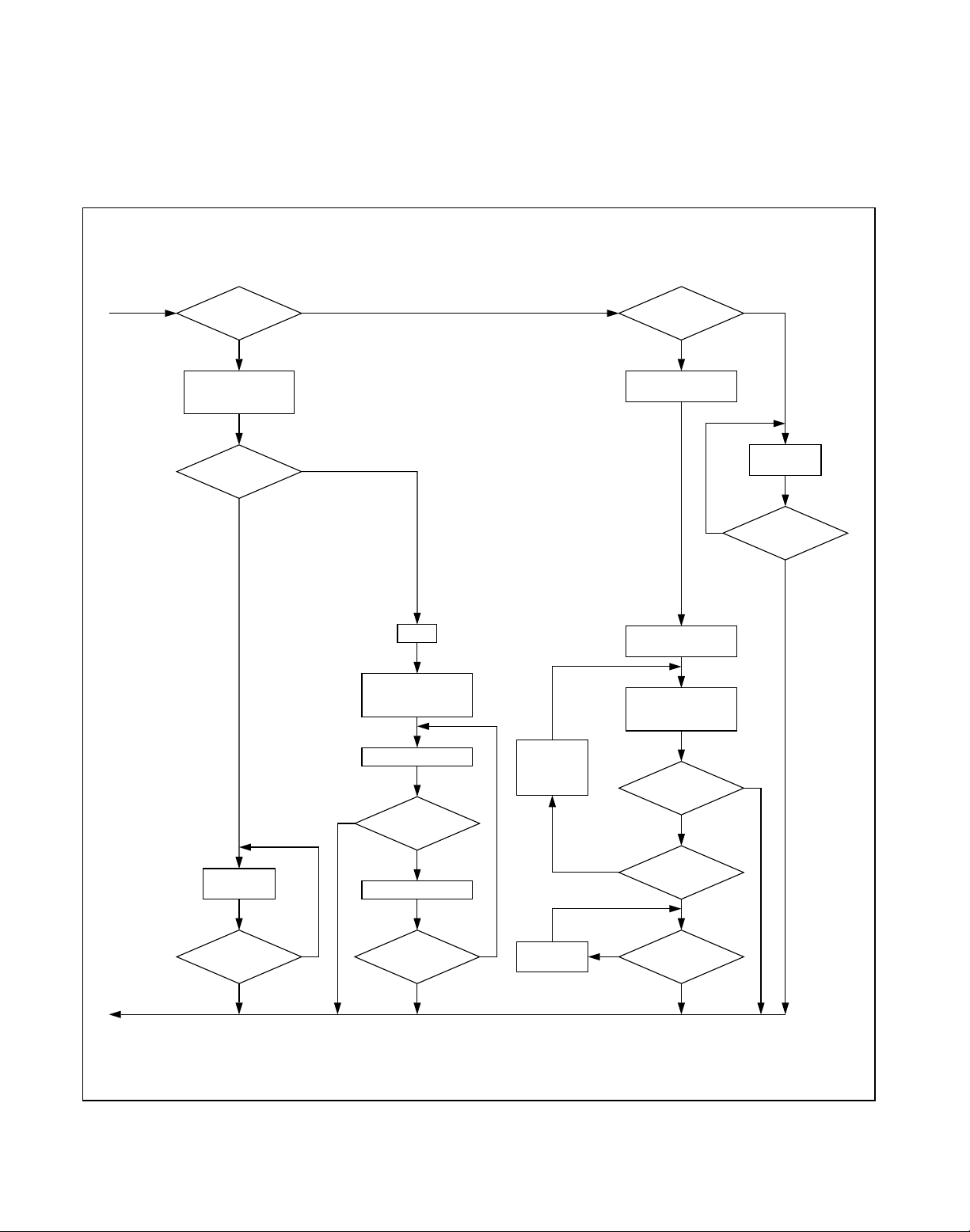
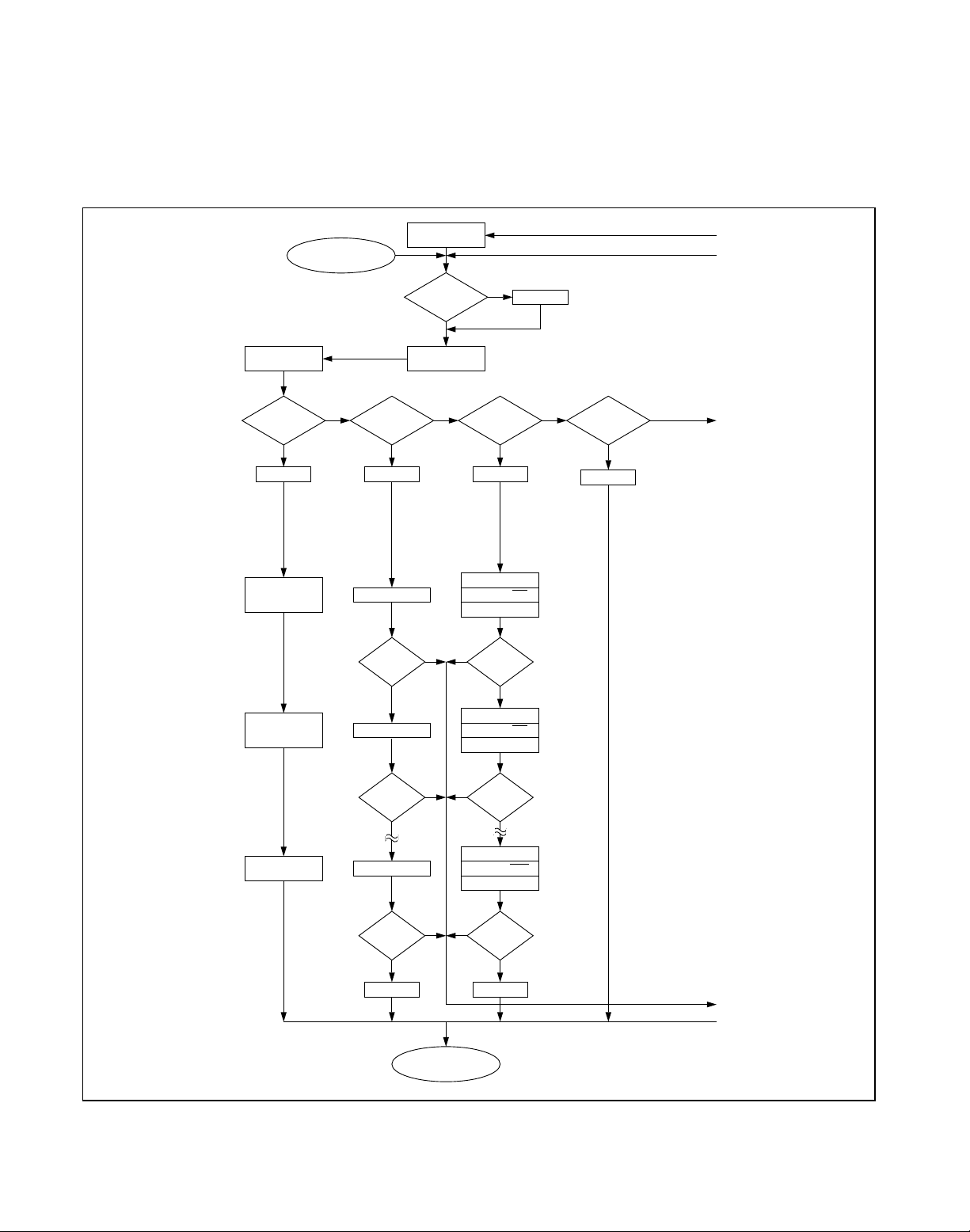
The
Memory Function Flowchart
(Figure 7) describes
the protocols necessary for accessing the memory of
the DS24B33. The target address registers TA1 and
TA2 are used for both read and write. The communication between the master and the DS24B33 takes place
either at standard speed (default, OD = 0) or at overdrive speed (OD = 1). If not explicitly set into the overdrive mode, the DS24B33 assumes standard speed.
Write Scratchpad [0Fh]
The Write Scratchpad command applies to the data
memory. After issuing the Write Scratchpad command,
the master must first provide the 2-byte target address,
followed by the data to be written to the scratchpad.
The data is written to the scratchpad starting at the byte
offset of T[4:0]. The ES bits E[4:0] are loaded with the
starting byte offset and increment with each subsequent byte. Effectively, E[4:0] is the byte offset of the
last full byte written to the scratchpad. Only full bytes
are accepted. If the last byte is incomplete, its content
is ignored and PF is set.
When executing the Write Scratchpad command, the
CRC generator inside the DS24B33 (Figure 13) calculates a 16-bit CRC of the entire data stream, starting at
the command code and ending at the last data byte as
sent by the master. This CRC is generated using the
CRC-16 polynomial (X
16
+ X
15
+ X2 + 1) by first clearing the CRC generator and then shifting in the command code (0Fh) of the Write Scratchpad command,
the target addresses TA1 and TA2 as supplied by the
master, and all the data bytes. The master can end the
Write Scratchpad command at any time. However, if the
end of the scratchpad is reached (E[4:0] = 11111b),
the master can send 16 read time slots to receive the
CRC generated by the DS24B33.
The DS24B33’s memory address range is 0000h to
01FFh. If the bus master sends a target address higher
than this, the DS24B33’s internal circuitry sets the 7
most significant address bits to zero as they are shifted
into the internal address register. The Read Scratchpad
command reveals the modified target address. The
master identifies such address modifications by comparing the target address read back to the target
address transmitted. If the master does not read the
scratchpad, a subsequent Copy Scratchpad command
does not work because the most significant bits of the
target address the master sends do not match the
value that the DS24B33 expects.
Read Scratchpad [AAh]
The Read Scratchpad command allows for verifying the
target address and the integrity of the scratchpad data.
After issuing the command code, the master begins
reading. The first 2 bytes are the target address. The
next byte is the ending offset/data status byte (E/S) followed by the scratchpad data beginning at the byte offset (T[4:0]). The master should read through the end of
the scratchpad. If the master continues reading beyond
the end of the scratchpad, all data are logic 1s.
Copy Scratchpad [55h]
The Copy Scratchpad command is used to copy data
from the scratchpad to the data memory. After issuing
the Copy Scratchpad command, the master must provide a 3-byte authorization pattern, which should have
been obtained by an immediately preceding Read
Scratchpad command. This 3-byte pattern must exactly
match the data contained in the three address registers
(TA1, TA2, E/S, in that order). If the pattern matches
and the target address is valid, the AA flag is set and
the copy begins. The data to be copied is determined
by the three address registers. The scratchpad data
from the beginning offset through the ending offset is
copied to memory, starting at the target address.
Anywhere from 1 to 32 bytes can be copied with this
command. The duration of the device’s internal data
transfer is t
PROG
, during which the voltage on the
1-Wire bus must not fall below V
PUPMIN
. A pattern of
alternating 0s and 1s are transmitted after the data has
been copied until the master issues a reset pulse.
Note: Because of the memory architecture of the
DS24B33, if a Copy Scratchpad command is interrupted
during the write cycle, two consecutive Copy
Scratchpad commands of the same data to the same
location may be necessary to recover. To verify the success of the Copy Scratchpad command, always look for
the alternating 0-to-1 pattern at the end of the Copy
Scratchpad command flow and also read back the EEPROM page that was to be updated. If the alternating
pattern appeared and the EEPROM page data shows
the intended new data, the write access was successful.
No further action is required. In all other cases (alternating 0-to-1 pattern is not seen or nonmatching EEPROM
page data), repeat the Write Scratchpad, Copy
Scratchpad sequence until successful.
Maxim Integrated
9
DS24B33

1-Wire 4Kb EEPROM
Figure 7a. Memory Function Flowchart
10
Maxim Integrated
DS24B33
DS24B33
INCREMENTS
SCRATCHPAD
OFFSET
BUS MASTER Tx MEMORY
FUNCTION COMMAND
0Fh
WRITE SCRATCHPAD?
DS24B33 CLEARS PF, AA
BUS MASTER Tx EEPROM
ARRAY TARGET ADDRESS
TA1 (T[7:0]), TA2 (T[15:8])
DS24B33 SETS SCRATCHPAD
OFFSET = (T[4:0])
MASTER Tx DATA BYTE
TO SCRATCHPAD OFFSET
DS24B33 SETS (E[4:0]) =
SCRATCHPAD OFFSET
MASTER Tx RESET?
N
SCRATCHPAD OFFSET
= 11111b?
FROM ROM FUNCTIONS
FLOWCHART (FIGURE 9)
N
Y
DS24B33
INCREMENTS
SCRATCHPAD
OFFSET
Y
N
Y
PARTIAL BYTE?
Y
PF = 1
N
N
AAh
READ SCRATCHPAD?
Y
BUS MASTER Rx
TA1 (T[7:0]), TA2 (T[15:8]),
AND E/S BYTE
DS24B33 SETS SCRATCHPAD
OFFSET = (T[4:0])
BUS MASTER Rx DATA BYTE
TO SCRATCHPAD OFFSET
MASTER Tx RESET?
N
SCRATCHPAD OFFSET
= 11111b?
Y
N
Y
TO FIGURE 7b
BUS MASTER
Rx "1"s
DS24B33 Tx CRC-16 OF
COMMAND, ADDRESS,
AND DATA BYTES AS THEY
WERE SENT BY THE BUS
MASTER
N
MASTER Tx RESET?
Y
TO ROM FUNCTIONS
FLOWCHART (FIGURE 9)
BUS MASTER
Rx "1"s
N
MASTER Tx RESET?
Y
FROM FIGURE 7b
1-Wire 4Kb EEPROM
Figure 7b. Memory Function Flowchart (continued)
Maxim Integrated
11
DS24B33
FROM FIGURE 7a
55h
COPY SCRATCHPAD?
Y
BUS MASTER Rx
TA1 (T[7:0]), TA2 (T[15:8]),
AND E/S BYTE
AUTHORIZATION
CODE MATCH?
N
N
Y
N
AA = 1
DS24B33 COPIES
SCRATCHPAD DATA
TO ADDRESS
DS24B33 Tx "0"
*
DS24B33
INCREMENTS
ADDRESS
COUNTER
F0h
READ MEMORY?
Y
BUS MASTER Tx
TA1 (T[7:0]), TA2 (T[15:8])
N
DS24B33 SETS MEMORY
ADDRESS = (T[15:0])
BUS MASTER Rx
DATA BYTE FROM
MEMORY ADDRESS
MASTER Tx RESET?
N
BUS MASTER
Rx "1"s
MASTER Tx RESET?
Y
Y
TO FIGURE 7a
BUS MASTER
Rx "1"s
MASTER Tx RESET?
Y
*1-Wire IDLE HIGH FOR t
Y
MASTER Tx RESET?
N
DS24B33 Tx "1"
N
FOR POWER.
PROG
MASTER Tx RESET?
Y
N
BUS MASTER
Rx "1"s
Y
N
N
ADDRESS < 1FFh?
N
MASTER Tx RESET?
Y

1-Wire 4Kb EEPROM
Read Memory [F0h]
The Read Memory command is the general function to
read from the DS24B33. After issuing the command,
the master must provide a 2-byte target address, which
should be in the range of 0000h to 01FFh. If the target
address is higher than 01FFh, the DS24B33 changes
the upper 7 address bits to 0. After the address is
transmitted, the master reads data starting at the (modified) target address and can continue until address
01FFh. If the master continues reading, the result is
FFh. The Read Memory command can be ended at any
point by issuing a reset pulse. Note that the (modified)
target address provided with the Read Memory command overwrites the target address that was specified
with a previously issued Write Scratchpad command.
The Read Memory command overwrites the scratchpad
with data from the target memory page. When reading
the last byte of a memory page, the scratchpad is
loaded with data from the next memory page. This
could cause unexpected data to be loaded into the
scratchpad.
1-Wire Bus System
The 1-Wire bus is a system that has a single bus master
and one or more slaves. In all instances the DS24B33 is
a slave device. The bus master is typically a microcontroller. The discussion of this bus system is broken
down into three topics: hardware configuration, transaction sequence, and 1-Wire signaling (signal types
and timing). The 1-Wire protocol defines bus transactions in terms of the bus state during specific time slots,
which are initiated on the falling edge of sync pulses
from the bus master.
Hardware Configuration
The 1-Wire bus has only a single line by definition; it is
important that each device on the bus be able to drive
it at the appropriate time. To facilitate this, each device
attached to the 1-Wire bus must have open-drain or
three-state outputs. The 1-Wire port of the DS24B33 is
open drain with an internal circuit equivalent to that
shown in Figure 8.
Rx
R
PUP
I
L
V
PUP
BUS MASTER
OPEN-DRAIN
PORT PIN
100Ω MOSFET
Tx
Rx
Tx
DATA
DS24B33 1-Wire PORT
Rx = RECEIVE
Tx = TRANSMIT
Figure 8. Hardware Configuration
12
Maxim Integrated
DS24B33

1-Wire 4Kb EEPROM
A multidrop bus consists of a 1-Wire bus with multiple
slaves attached. The DS24B33 supports both a standard and overdrive communication speed of 15.4kbps
(maximum) and 125kbps (maximum), respectively, over
the full pullup voltage range. For pullup voltages of
+4.75V and higher, the DS24B33 also supports the
legacy communication speed of 16.3kbps and overdrive speed of 142kbps. The slightly reduced rates for
the DS24B33 are a result of additional recovery times,
which in turn were driven by a 1-Wire physical interface
enhancement to improve noise immunity. The value of
the pullup resistor primarily depends on the network
size and load conditions. The DS24B33 requires a
pullup resistor of 2.2kΩ (maximum) at any speed.
The idle state for the 1-Wire bus is high. If for any reason a transaction must be suspended, the bus
must
be
left in the idle state if the transaction is to resume. If this
does not occur and the bus is left low for more than
16µs (overdrive speed) or more than 120µs (standard
speed), one or more devices on the bus may be reset.
Transaction Sequence
The protocol for accessing the DS24B33 through the
1-Wire port is as follows:
• Initialization
• ROM Function Commands
• Memory Function Commands
• Transaction/Data
Initialization
All transactions on the 1-Wire bus begin with an initialization sequence. The initialization sequence consists
of a reset pulse transmitted by the bus master followed
by presence pulse(s) transmitted by the slave(s). The
presence pulse lets the bus master know that the
DS24B33 is on the bus and is ready to operate. For
more details, see the
1-Wire Signaling
section.
1-Wire ROM Function Commands
Once the bus master has detected a presence, it can
issue one of the seven ROM function commands that
the DS24B33 supports. All ROM function commands are
8 bits long. See Figure 9 for a list of these commands.
Read ROM [33h]
This command allows the bus master to read the
DS24B33’s 8-bit family code, unique 48-bit serial number, and 8-bit CRC. This command can only be used if
there is a single slave on the bus. If more than one
slave is present on the bus, a data collision occurs
when all slaves try to transmit at the same time (open
drain produces a wired-AND result). The resultant family
code and 48-bit serial number results in a mismatch of
the CRC.
Match ROM [55h]
The Match ROM command, followed by a 64-bit ROM
sequence, allows the bus master to address a specific
DS24B33 on a multidrop bus. Only the DS24B33 that
exactly matches the 64-bit ROM sequence responds to
the memory function command that follows. All other
slaves wait for a reset pulse. This command can be
used with a single device or multiple devices on the
bus.
Search ROM [F0h]
When a system is initially brought up, the bus master
might not know the number of devices on the 1-Wire
bus or their registration numbers. By taking advantage
of the bus’s wired-AND property, the master can use a
process of elimination to identify the registration numbers of all slave devices. For each bit of the registration
number, starting with the LSB, the bus master issues a
triplet of time slots. On the first slot, each slave device
participating in the search outputs the true value of its
registration number bit. On the second slot, each slave
device participating in the search outputs the complemented value of its registration number bit. On the third
slot, the master writes the true value of the bit to be
selected. All slave devices that do not match the bit
written by the master stop participating in the search. If
both of the read bits are zero, the master knows that
slave devices exist with both states of the bit. By choosing which state to write, the bus master branches in the
ROM code tree. After one complete pass, the bus master knows the registration number of a single device.
Additional passes identify the registration numbers of
the remaining devices. Refer to Application Note 187:
1-Wire Search Algorithm
for a detailed discussion and
an example.
Maxim Integrated
13
DS24B33

1-Wire 4Kb EEPROM
Skip ROM [CCh]
This command can save time in a single-drop bus system by allowing the bus master to access the memory
functions without providing the 64-bit ROM code. If
more than one slave is present on the bus and, for
example, a read command is issued following the Skip
ROM command, data collision occurs on the bus as
multiple slaves transmit simultaneously (open-drain
pulldowns produce a wired-AND result).
Resume [A5h]
To maximize the data throughput in a multidrop environment, the Resume command is available. This command checks the status of the RC bit and, if it is set,
directly transfers control to the memory functions, similar to a Skip ROM command. The only way to set the
RC bit is by successfully executing the Match ROM,
Search ROM, or Overdrive-Match ROM command.
Once the RC bit is set, the device can repeatedly be
accessed through the Resume command. Accessing
another device on the bus clears the RC bit, preventing
two or more devices from simultaneously responding to
the Resume command.
Overdrive-Skip ROM [3Ch]
On a single-drop bus, this command can save time by
allowing the bus master to access the memory functions without providing the 64-bit ROM code. Unlike the
normal Skip ROM command, the Overdrive-Skip ROM
command sets the DS24B33 in the overdrive mode (OD
= 1). All communication following this command must
occur at overdrive speed until a reset pulse of minimum
480µs duration resets all devices on the bus to standard speed (OD = 0).
When issued on a multidrop bus, this command sets all
overdrive-supporting devices into overdrive mode. To
subsequently address a specific overdrive-supporting
device, a reset pulse at overdrive speed must be
issued followed by a Match ROM or Search ROM command sequence. This speeds up the time for the
search process. If more than one slave supporting
overdrive is present on the bus and the Overdrive-Skip
ROM command is followed by a Read command, data
collision occurs on the bus as multiple slaves transmit
simultaneously (open-drain pulldowns produce a wiredAND result).
Overdrive-Match ROM [69h]
The Overdrive-Match ROM command followed by a 64bit ROM sequence transmitted at overdrive speed
allows the bus master to address a specific DS24B33
on a multidrop bus and to simultaneously set it in overdrive mode. Only the DS24B33 that exactly matches
the 64-bit ROM sequence responds to the subsequent
memory function command. Slaves already in overdrive
mode from a previous Overdrive-Skip ROM or successful Overdrive-Match ROM command remain in overdrive mode. All overdrive-capable slaves return to
standard speed at the next reset pulse of minimum
480µs duration. The Overdrive-Match ROM command
can be used with a single device or multiple devices on
the bus.
14
Maxim Integrated
DS24B33
1-Wire 4Kb EEPROM
FROM MEMORY FUNCTIONS
Figure 9a. ROM Functions Flowchart
Maxim Integrated
15
DS24B33
FLOWCHART (FIGURE 7)
BUS MASTER Tx
RESET PULSE
FROM FIGURE 9b
BUS MASTER Tx ROM
FUNCTION COMMAND
33h
READ ROM
COMMAND?
Y
RC = 0
DS24B33Tx
FAMILY CODE
(1 BYTE)
DS24B33 Tx
SERIAL NUMBER
(6 BYTES)
RESET PULSE?
DS24B33 Tx
PRESENCE PULSE
N
55h
MATCH ROM
COMMAND?
RC = 0 RC = 0
MASTER Tx BIT 0
BIT 0 MATCH? BIT 0 MATCH?
MASTER Tx BIT 1
N N
Y
OD
Y
N
N
F0h
SEARCH ROM
COMMAND?
YY
DS24B33 Tx BIT 0
DS24B33 Tx BIT 0
MASTER Tx BIT 0
Y
DS24B33 Tx BIT 1
DS24B33 Tx BIT 1
MASTER Tx BIT 1
OD = 0
NN
CCh
SKIP ROM
COMMAND?
Y
RC = 0
TO FIGURE 9b
DS24B33 Tx
CRC BYTE
BIT 1 MATCH?
Y
MASTER Tx BIT 63
BIT 63 MATCH?
Y
RC = 1
TO MEMORY FUNCTIONS
N N
DS24B33 Tx BIT 63
DS24B33 Tx BIT 63
MASTER Tx BIT 63
N N
FLOWCHART (FIGURE 7)
BIT 1 MATCH?
Y
BIT 63 MATCH?
Y
RC = 1
TO FIGURE 9b
FROM FIGURE 9b

1-Wire 4Kb EEPROM
Figure 9b. ROM Functions Flowchart (continued)
16
Maxim Integrated
DS24B33
TO FIGURE 9a
FROM FIGURE 9a
A5h
RESUME
COMMAND?
Y
RC = 1?
Y
N
N
MASTER Tx
RESET?
N
3Ch
OVERDRIVE-
SKIP ROM?
RC = 0; OD = 1 RC = 0; OD = 1
MASTER Tx
RESET?
Y
N
Y
Y
N
69h
OVERDRIVE-
MATCH ROM?
Y
MASTER Tx BIT 0
BIT 0 MATCH?
Y
MASTER Tx BIT 1
BIT 1 MATCH?
Y
MASTER Tx BIT 63
N
(SEE NOTE)
N
OD = 0
(SEE NOTE)
N
OD = 0
(SEE NOTE)
BIT 63 MATCH?
FROM FIGURE 9a
TO FIGURE 9a
NOTE: THE OD FLAG REMAINS AT 1 IF THE DEVICE WAS ALREADY AT OVERDRIVE SPEED BEFORE THE OVERDRIVE-MATCH ROM COMMAND WAS ISSUED.
RC = 1
N
OD = 0
Y

1-Wire 4Kb EEPROM
1-Wire Signaling
The DS24B33 requires strict protocols to ensure data
integrity. The protocol consists of four types of signaling
on one line: reset sequence with reset pulse and presence pulse, write-zero, write-one, and read-data.
Except for the presence pulse, the bus master initiates
all falling edges. The DS24B33 can communicate at
two different speeds: standard speed and overdrive
speed. If not explicitly set into the overdrive mode, the
DS24B33 communicates at standard speed. While in
overdrive mode the fast timing applies to all waveforms.
To get from idle to active, the voltage on the 1-Wire line
needs to fall from V
PUP
below the threshold VTL. To get
from active to idle, the voltage needs to rise from
V
ILMAX
past the threshold VTH. The time it takes for the
voltage to make this rise is seen in Figure 10 as ε, and
its duration depends on the pullup resistor (R
PUP
) used
and the capacitance of the 1-Wire network attached.
The voltage V
ILMAX
is relevant for the DS24B33 when
determining a logical level, not triggering any events.
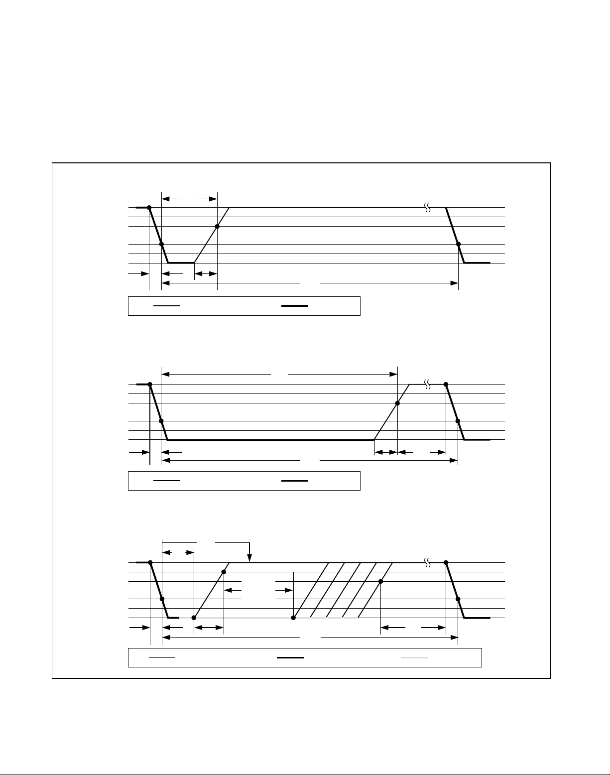
Figure 10 shows the initialization sequence required to
begin any communication with the DS24B33. A reset
pulse followed by a presence pulse indicates that the
DS24B33 is ready to receive data, given the correct
ROM and memory function command. If the bus master
uses slew-rate control on the falling edge, it must pull
down the line for t
RSTL
+ tF to compensate for the edge.
A t
RSTL
duration of 480µs or longer exits the overdrive
mode, returning the device to standard speed. If the
DS24B33 is in overdrive mode and t
RSTL
is no longer
than 80µs, the device remains in overdrive mode. If the
device is in overdrive mode and t
RSTL
is between 80µs
and 480µs, the device resets, but the communication
speed is undetermined.
After the bus master has released the line it goes into
receive mode. Now the 1-Wire bus is pulled to V
PUP
through the pullup resistor, or in case of a DS2482-x00
or DS2480B driver, by active circuitry. When the threshold V
TH
is crossed, the DS24B33 waits for t
PDH
and
then transmits a presence pulse by pulling the line low
for t
PDL
. To detect a presence pulse, the master must
test the logical state of the 1-Wire line at t
MSP
.
The t
RSTH
window must be at least the sum of t
PDHMAX
,
t
PDLMAX
, and t
RECMIN
. Immediately after t
RSTH
is
expired, the DS24B33 is ready for data communication.
In a mixed population network, t
RSTH
should be extended to minimum 480µs at standard speed and 48µs at
overdrive speed to accommodate other 1-Wire devices.
Read/Write Time Slots
Data communication with the DS24B33 takes place in
time slots, which carry a single bit each. Write time slots
transport data from bus master to slave. Read time
slots transfer data from slave to master. Figure 11 illustrates the definitions of the write and read time slots.
All communication begins with the master pulling the
data line low. As the voltage on the 1-Wire line falls
below the threshold VTL, the DS24B33 starts its internal
timing generator that determines when the data line is
sampled during a write time slot and how long data is
valid during a read time slot.
Master-to-Slave
For a write-one time slot, the voltage on the data line
must have crossed the V
TH
threshold before the write-
one low time t
W1LMAX
is expired. For a write-zero time
slot, the voltage on the data line must stay below the
V
TH
threshold until the write-zero low time t
W0LMIN
is
expired. For the most reliable communication, the
RESISTOR MASTER DS24B33
t
RSTL
t
PDL
t
RSTH
t
PDH
MASTER Tx "RESET PULSE" MASTER Rx "PRESENCE PULSE"
V
PUP
V
IHMASTER
V
TH
V
TL
V
ILMAX
0V
ε
t
F
t
REC
t
MSP
Figure 10. Initialization Procedure: Reset and Presence Pulse
Maxim Integrated
17
DS24B33
1-Wire 4Kb EEPROM
voltage on the data line should not exceed V
ILMAX
dur-
ing the entire t
W0L
or t
W1L
window. After the V
TH
thresh-
old has been crossed, the DS24B33 needs a recovery
time t
REC
before it is ready for the next time slot.
RESISTOR MASTER
RESISTOR MASTER
RESISTOR MASTER DS24B33
ε
ε
δ
V
PUP
V
IHMASTER
V
TH
V
TL
V
ILMAX
0V
t
F
V
PUP
V
IHMASTER
V
TH
V
TL
V
ILMAX
0V
t
F
V
PUP
V
IHMASTER
V
TH
V
TL
V
ILMAX
0V
t
F
t
SLOT
t
W1L
t
REC
t
SLOT
t
SLOT
t
W0L
t
REC
MASTER
SAMPLING
WINDOW
t
RL
t
MSR
WRITE-ONE TIME SLOT
WRITE-ZERO TIME SLOT
READ-DATA TIME SLOT
Figure 11. Read/Write Timing Diagrams
18
Maxim Integrated
DS24B33

1-Wire 4Kb EEPROM
Slave-to-Master
A read-data time slot begins like a write-one time slot.
The voltage on the data line must remain below V
TL
until the read low time t
RL
is expired. During the t
RL
window, when responding with a 0, the DS24B33 starts
pulling the data line low; its internal timing generator
determines when this pulldown ends and the voltage
starts rising again. When responding with a 1, the
DS24B33 does not hold the data line low at all, and the
voltage starts rising as soon as t
RL
is over.
The sum of t
RL
+ δ (rise time) on one side and the inter-
nal timing generator of the DS24B33 on the other side
define the master sampling window (t
MSRMIN
to
t
MSRMAX
) in which the master must perform a read from
the data line. For the most reliable communication, t
RL
should be as short as permissible, and the master
should read close to but no later than t
MSRMAX
. After
reading from the data line, the master must wait until
t
SLOT
is expired. This guarantees sufficient recovery
time t
REC
for the DS24B33 to get ready for the next time
slot. Note that t
REC
specified herein applies only to a
single DS24B33 attached to a 1-Wire line. For multidevice configurations, t
REC
needs to be extended to
accommodate the additional 1-Wire device input
capacitance. Alternatively, an interface that performs
active pullup during the 1-Wire recovery time such as
the DS2482-x00 or DS2480B 1-Wire line drivers can be
used.
Improved Network Behavior
(Switchpoint Hysteresis)
In a 1-Wire environment, line termination is possible
only during transients controlled by the bus master
(1-Wire driver). 1-Wire networks, therefore, are susceptible to noise of various origins. Depending on the physical size and topology of the network, reflections from
end points and branch points can add up or cancel
each other to some extent. Such reflections are visible
as glitches or ringing on the 1-Wire communication line.
Noise coupled onto the 1-Wire line from external
sources can also result in signal glitching. A glitch during the rising edge of a time slot can cause a slave
device to lose synchronization with the master and,
consequently, result in a Search ROM command coming to a dead end or cause a device-specific function
command to abort. For better performance in network
applications, the DS24B33 uses an improved 1-Wire
front-end, which makes it less sensitive to noise.
The 1-Wire front-end of the DS24B33 differs from traditional slave devices in one characteristic: There is a hysteresis at the low-to-high switching threshold V
TH
. If a
negative glitch crosses V
TH
but does not go below
VTH- VHY, it is not recognized (Figure 12). The hysteresis
is effective at any 1-Wire speed.
CRC Generation
The DS24B33 uses two different types of CRCs. One
CRC is an 8-bit type and is stored in the most significant byte of the 64-bit registration number. The bus
master can compute a CRC value from the first 56 bits
of the 64-bit registration number and compare it to the
value stored within the DS24B33 to determine if the registration number has been received error-free. The
equivalent polynomial function of this CRC is X
8
+ X5 +
X
4
+ 1. This 8-bit CRC is received in the true (noninverted) form. It is computed and programmed into the chip
at the factory.
The other CRC is a 16-bit type, generated according to
the standardized CRC-16 polynomial function X
16
+ X
15
+ X2 + 1. This CRC is used for fast verification of a data
transfer when writing to the scratchpad. In contrast to
the 8-bit CRC, the 16-bit CRC is always communicated
in the inverted form. A CRC generator inside the
DS24B33 (Figure 13) calculates a new 16-bit CRC, as
shown in the command flowchart (Figure 7). The bus
master compares the CRC value read from the device
to the one it calculates from the data, and decides
whether to continue with an operation.
With the Write Scratchpad command, the CRC is generated by first clearing the CRC generator and then
shifting in the command code, the target addresses
TA1 and TA2, and all the data bytes as they were sent
by the bus master. The DS24B33 transmits this CRC
only if the data bytes written to the scratchpad include
scratchpad ending offset 11111b. The data can start at
any location within the scratchpad.
For more information on generating CRC values refer to
Application Note 27:
Understanding and Using Cyclic
Redundancy Checks with Maxim iButton Products
.
V
PUP
V
TH
V
HY
0V
Figure 12. Hysteresis at the Low-to-High Switching Threshold
Maxim Integrated
19
DS24B33
1-Wire 4Kb EEPROM
Figure 13. CRC-16 Hardware Description and Polynomial
Command-Specific 1-Wire Communication Protocol—Legend
20
Maxim Integrated
DS24B33
POLYNOMIAL = X16 + X15 + X2 + 1
1ST
STAGE
0
X
9TH
STAGE
8
X
2ND
STAGE
1
X
10TH
STAGE
9
X
11TH
STAGE
10
X
3RD
STAGE
2
X
12TH
STAGE
11
X
4TH
STAGE
3
X
13TH
STAGE
12
X
5TH
STAGE
4
X
14TH
STAGE
13
X
6TH
STAGE
5
X
15TH
STAGE
14
X
7TH
STAGE
6
X
7
X
15
X
INPUT DATA
STAGE
16TH
STAGE
8TH
16
X
SYMBOL DESCRIPTION
RST 1-Wire reset pulse generated by master
PD 1-Wire presence pulse generated by slave
Select Command and data to sati sf y the ROM function protocol
WS Command: “Write Scratchpad”
RS Command: “Read Scratchpad”
CPS Command: “Copy Scratchpad”
RM Command: “Read Memory”
TA Target Address TA1, TA2
TA-E/S Target Address TA1, TA2 with E/S byte
<data to EOS> Transfer of as many bytes as needed to reach the end of the scratchpad for a given target address
<data to EOM> Transfer of as man y byte s as are needed to reach the end of the memory
CRC-16 Transfer of an in verted CRC-16
FF loop Indefin ite loop where the master reads FF bytes
AA loop Indefinite loop where the ma ster reads AA byte s
Programm ing Data transfer to EEPROM; no activity on the 1-Wire bus permitted during this time
CRC OUTPUT

1-Wire 4Kb EEPROM
Command-Specific 1-Wire Communication Protocol—Color Codes
1-Wire Communication Examples
Maxim Integrated
21
DS24B33
Master-to-Slave Slave-to-Master Programming
Write Scratchpad, Reaching the End of the Scratchpad
RST WS
PD TASelect <data to EOS> FF loopCRC-16
Read Scratchpad
RST RSPD TA-E/SSelect <data to EOS>
Copy Scratchpad (Success)
RST CPSPD TA-E/SSelect AA loop
Programming
FF loop
Copy Scratchpad (Fail TA-E/S)
RST CPSPD TA-E/SSelect FF loop
Read Memory
RST RM TAPD Select FF loop
<data to EOM>

1-Wire 4Kb EEPROM
Package Information
For the latest package outline information and land patterns (footprints), go to www.maxim-ic.com/packages. Note that a “+”, “#”, or
“-” in the package code indicates RoHS status only. Package drawings may show a different suffix character, but the drawing pertains
to the package regardless of RoHS status.
SFN Package Orientation on Tape and Reel
PACKAGE TYPE PACKAGE CODE OUTLINE NO.
LAND
PATTERN NO.
8 SO W8+2
21-0262
90-0258
3 TO-92 (Bulk) Q3+1
21-0248
—
3 TO-92 (T&R) Q3+4
21-0250
—
2 SFN G266N+1
21-0390
—
6 TDFN-EP T633+2
21-0137
90-0058
22
Maxim Integrated
DS24B33
LEADS FACE UP IN ORIENTATION SHOWN ABOVE.
USER DIRECTION OF FEED
SFN
(6mm × 6mm × 0.9mm)

1-Wire 4Kb EEPROM
Revision History
23
Maxim Integrated 160 Rio Robles, San Jose, CA 95134 USA 1-408-601-1000
Maxim cannot assume responsibility for use of any circuitry other than circuitry entirely embodied in a Maxim product. No circuit patent licenses are implied.
Maxim reserves the right to change the circuitry and specifications without notice at any time. The parametric values (min and max limits) shown in the Electrical
Characteristics table are guaranteed. Other parametric values quoted in this data sheet are provided for guidance.
©
2012 Maxim Integrated
The Maxim logo and Maxim Integrated are trademarks of Maxim Integrated Products, Inc.
DS24B33
REVISION
NUMBER
0 2/11 Initia l release —
1 5/11 Implemented text changes to better market the document 1
2 3/12 Revised the Electrical Characterist ic s table notes 1, 5, and 15. 3
3 5/12 Added the SFN (6mm x 6mm x 0.9mm) and TDFN (3mm x 3mm) packages 1, 2, 4, 5, 22
REVISION
DATE
DESCRIPTION
CHANGED
PAGES
 Loading...