

Page 1

P8F151
MOTHER BOARD
USER’S MANUAL
Page 2

Copyright Notice
©
Copyright 2002
The information contained in this user’ s manualand all accompanying documentation is copyrighted and all rights are reserved.
This publication may not, in whole or in part, be reproduced,
transcribed, stored in a retrieval system, translated into any
language or computer language, or transmitted in any form
whatsoever without the prior written consent from the manufacturer, except for copies retained by the purchasers for their
personal archival purposes.
The manufacturer reserves the right to revise this user s manual
and all accompanying documentation and to make changes in the
content without obligation to notify any person or organization of
the revision or change.
IN NO EVENT WILL THE VENDOR BE LIABLE FOR DIRECT,
INDIRECT, SPECIAL, INCIDENTAL, OR CONSEQUENTIAL
DAMAGES ARISING OUT OF THE USE OR INABILITY TO USE
THIS PRODUCT OR DOCUMENTATION, EVEN IF ADVISED
OF THE POSSIBILITY OF SUCH DAMAGES. IN PARTICULAR,
THE VENDOR SHALL NOT HAVE LIABILITY FOR ANY HARDWARE, SOFTWARE, OR DATA STORED OR USED WITH THE
PRODUCT, INCLUDING THE COSTS OF REPAIRING, REPLACING, OR RECOVERING SUCH HARDWARE, SOFTWARE, OR DATA.
All trademarks mentioned in this document are acknowledged.
The specifications in this manual are subject to change without
notice.
Page 3

Using This Manual
This manual is designed to help you build a reliable Personal Computer
based on the P8F148 platform.
Chapter 1 - Quick Reference
This chapter is for advanced users who want to quickly assemble a system.
The mainboard layout along with jumper and switch settings, and memory
configuration are provided.
Chapter 2 - Introduction
This chapter includes an introduction, a checklist of the items that ship
with this mainboard, and a summary of the principal features and components.
Chapter 3 - Hardware Installation
This chapter explains how to prepare your mainboard for use and how to
make the various connections to other computer components and peripheral items.
Chapter 4 - BIOS Configuration
This chapter explains how to use the system setup utility that is stored in
the mainboard’ s firmware.
Chapter 5 - Driver and Utility
This chapter briefly describes the drivers and utility programs that are
packaged with the mainboard.
ii
Page 4

Table of Contents
1. P8F151 QUICK REFERENCE ................................................ 1
1.1. Mainboard Layout ............................................................. 1
1.2. I/O Ports ...........................................................................2
1.3. Front Panel Connector ..................................................... 2
1.4. Jumpers ...........................................................................3
1.5. PCI and AGP Frequency Settings .................................... 3
1.6. Memory Installation ...........................................................3
1.7. Connectors.......................................................................4
2. INTRODUCTION .................................................................... 5
2.1. Overview .......................................................................... 5
2.2. Mainboard Specifications and Features ........................... 6
2.2.1. Hardware ............................................................................. 6
2.2.2. Software .............................................................................. 8
2.3. Mainboard Layout ............................................................. 9
2.4. Microprocessor .............................................................. 11
2.5. CPU Packaging .............................................................. 11
2.6. AC97 Codec ................................................................... 11
2.7. Chipset ........................................................................... 12
2.8. RAID (Optional) .............................................................. 13
3. HARDWARE INSTALLATION ............................................ 14
3.1. Unpacking....................................................................... 14
3.2. Installation.......................................................................15
3.3. Safety Measures ............................................................ 15
3.4. Connector/Jumper Location ...........................................16
3.5. Attaching Connectors ..................................................... 17
3.5.1. Front Panel Connectors (JP15) .......................................... 17
iii
Page 5

3.5.2. Infrared (IR) Connectors (JP2) .......................................... 18
3.5.3. LAN/Modem Wake up Connectors (JP9).......................... 18
3.5.4. Front USB Connectors (JP4, JP5) ...................................... 19
3.5.5. Floppy Drive Connector (FLOPPY)................................... 19
3.5.6. IDE Connectors (IDE1, IDE2, BIDE1, BIDE2) .................... 20
3.5.7. Back Panel Connectors ..................................................... 21
3.5.8. Power Supply Connector (ATX1) ..................................... 24
3.5.9. CPU/AGP/System FAN Power Supplies ........................... 25
3.5.10. PCI Connector (PCI1~PCI5) .............................................. 26
3.6. Installing the CPU ........................................................... 27
3.6.1. Before You Begin .............................................................. 27
3.6.2. Installation Procedure ....................................................... 27
3.6.3. Removing the Processor ................................................... 28
3.7. Installing System Memory .............................................. 29
3.8. Setting Jumpers .............................................................30
3.9. Auto Power On ............................................................... 31
4. BIOS CONFIGURATION ..................................................... 32
4.1. Entering Setup................................................................33
4.2. Standard CMOS Features..............................................35
4.3. Advanced BIOS Features...............................................38
4.4. Advanced Chipset Features ........................................... 41
4.5. Integrated Peripherals .................................................... 44
4.6. Power Management Setup .............................................48
4.7. PnP/PCI Configurations ................................................. 52
4.8. PC Health Status Option ................................................54
4.9. Frequency/Voltage Control ............................................. 56
4.10. Load Optimized Defaults Option .................................... 57
4.11. Set Supervisor/User Password ......................................58
4.12. Save & Exit Setup .......................................................... 59
iv
Page 6

4.13. Exit Without Saving ........................................................ 59
5. DRIVER AND UTILITY ....................................................... 60
5.1. Flash Utility ..................................................................... 60
5.2 CD Driver Overview ....................................................... 61
5.2.1. Intel Chipset 845 INF Driver .............................................. 62
5.2.2. Intel Chipset 845 Busmater IDE Driver .............................. 62
5.2.3. AD1881 Audio Driver ....................................................... 63
5.3. Online Services .............................................................. 64
v
Page 7
1. P8F151 Quick Reference
This section is for users to get started using the mainboard straight away.
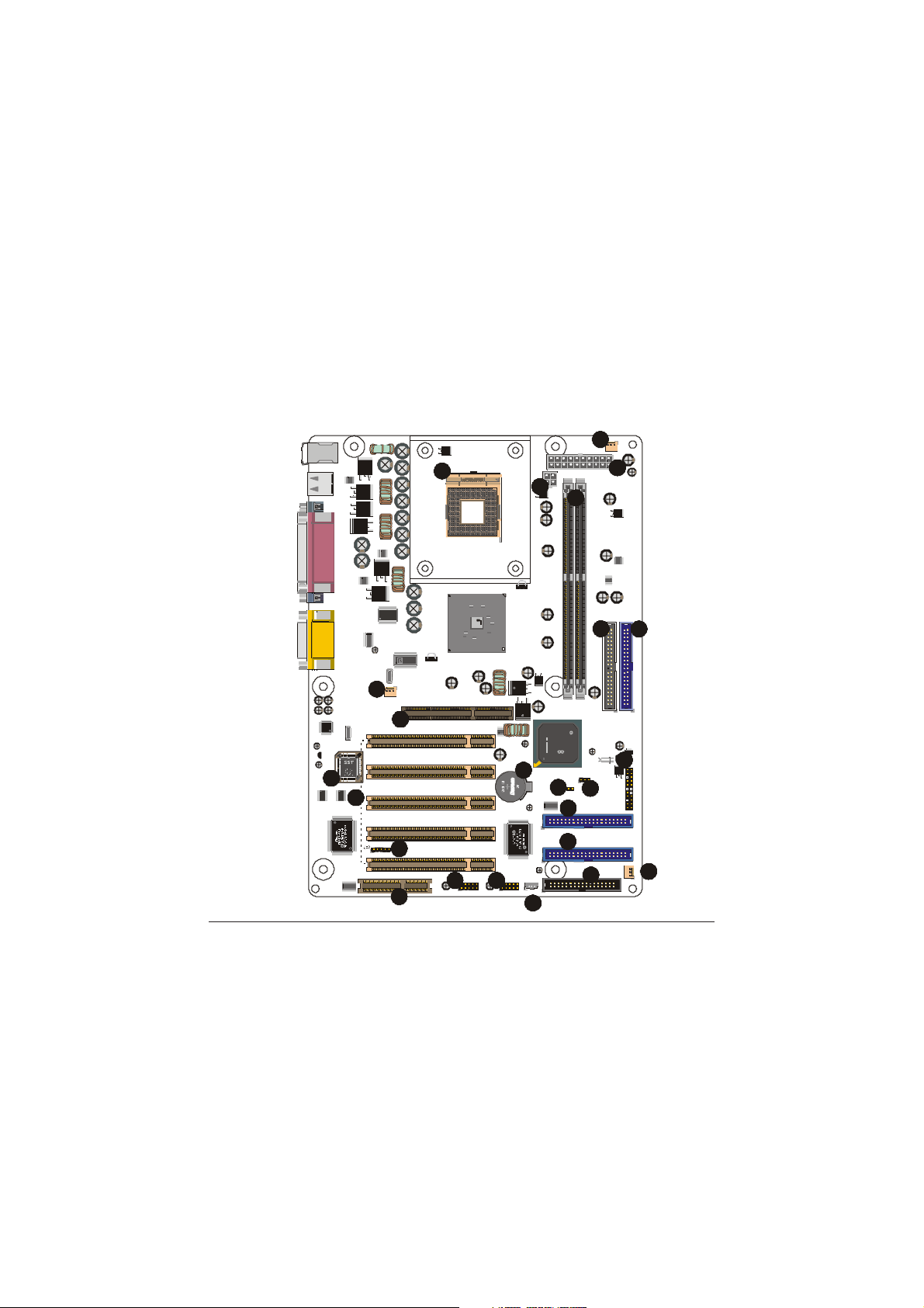
1.1. Mainboard Layout
PORTS
&
KB1
OUSE
KEYBOARD
M
PS/2
PS/2
USB1
PORTS
USB
COM1
&
PORTS
SERIAL
PARALLEL
1
LOTES
ATX1
JP10
3
ATXPOWER
ATX12V POWER
4
17
FAN 2
N
FA
S
Y
S
2
&
IC-IN
,M
UT
AME/MIDI PORTS
G
LINE- IN,L INE-O
AUDIO1
AUDIO CODEC
2M FLASHEPROM
21
6
I/OC HIPSET
C
UM7700 45
0149
950202C F
T
01
4.3
18
FAN 1
17
CPU FAN
AGP
5
PCI 1
PCI 2
PCI 3
PCI 4
IR
16
PCI 5
CNR
7
1. mPGA478 CPU socket (mPGA478)
2. ATX power connector (ATX1)
3. ATX 12V power connector (JP10)
4. 184-pin DIMM DDR module sockets (DIMM1~2)
5. Accelerated Graphics Port slot (AGP1)
6. PCI expansion connector (PCI 1 ~ PCI 5)
7. CNR connector (CNR)
8. IDE connector (IDE1)
9. IDE connector (IDE2)
10. RAID connector (BIDE1)
11. RAID connector (BIDE2)
Mainboard Layout
'01
M
C
L148
A320
RET
82SEC
QC
RG88BKEES
ET
CEB6030L
C
CEB6030L
ET
C
20
RAIDCH IPSET
C
R
USB2 USB1
14 14
JP4
JP9
WOL
JP5
15
12. Floppy drive connector (FLP)
13. Front Panel connectors (JP14)
14. Front USB ports connectors (JP4/JP5)
15. Wake on LAN connector (JP9)
16. IR connector (JP2)
17. FAN connectors (FAN1/FAN2/FAN3)
18. EMI-SMI (JP11 )
19. Clear CMOS (JP12)
20. RTC battery
21. Flash BIOS
in tel
SECERT
FW82801DB
L140IZ6Q
QC68ES
M C
INTE L '01
G135988VID
140KO REA
JP11
18
11
BIDE2
10
BIDE1
IR
FLP FLOPPY
DIM2DIM1
R
JP12
19
FAN2
12
JP5
13
89
IDE1IDE2
R
TO
C
E
N
N
O
C
L
E
N
A
P
T
N
O
FR
JP14
FA
N
3
17
1
Page 8
Mainboard Users Manual
(
)
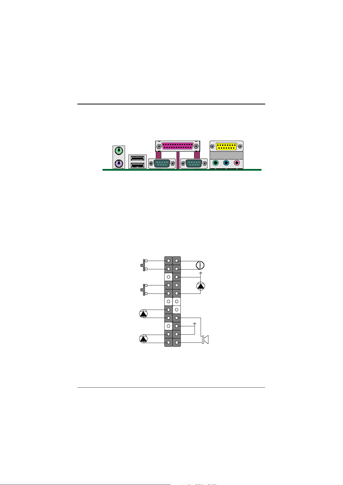
1.2. I/O Ports
PS/2 Mo us e port
PS/2 Ke yboard port
USB ports
Parallel p ort MIDI/G AME port
COM1 port
COM2 port
1.3. Front Panel Connector
The following illustration shows the front panel connector pin assignments:
(PWSW)
POWER SWITCH
(Reset)
RESET BUTTON
Grou nd
Power on/off
Grou nd
Rese t Sin gle
Grou nd
Keyboard
LED cat hode
Non
LED anode
Line-Out / Line-In / M ic-In ports
PWR LED & keylock
POWER LED
& KEYLOCK
(STB LED)
STA NDB Y LED
(HDD LED)
HDD LED
LED cat hode
LED anode
LED cat hode
LED anode
+5V
Grou nd
Non
Spea ke r-ou t
SPEAKE R
Pin 1
2
I/O Ports
Page 9
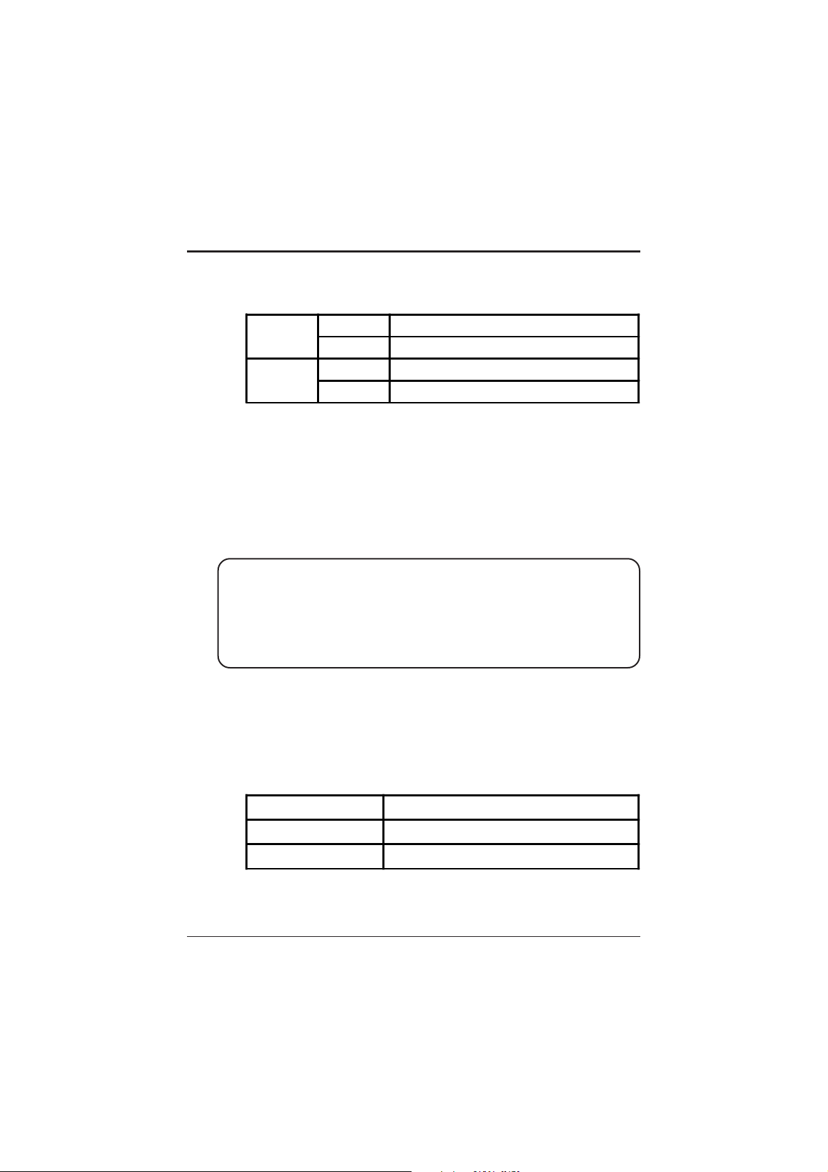
1.4 Jumpers
P8F151 Quick Reference
JP12
JP11
1-2 Normal Mode
2-3 Clear CMOS
Open
Cl ose D isable EXT-SMI
Enable EXT-SMI
1.5. PCI and AGP Frequency Setting
The PCI and AGP frequency settings are automatically set by the system
1.6. Memory Installation
Note: The Intel 845 chipset family used in this mainboard supports up
to two double-sided or two single-sided DIMMs when the DDR
DRAM interface is operating at 133 MHz. Installing DDR DIMM
modules that exceed these specifications requires that the BIOS
down-shifts the DRAM clocks to 100 MHz through a two-wire
interface of the system clock generator.
184-Pin DIMM DDR SDRAM Memory Configuration.
Jumper
Each 184-pin DIMM bank can install from 64MB up to 1GB
of PC1600/PC2100 compliant 2.5V single or double side unbuffered
with or without ECC DDR SDRAM modules.
Bank 0 (DIMM1) 64MB,128MB,256MB, 512MB, 1GB
Bank 1 (DIMM2) 64MB,128MB,256MB, 512MB, 1GB
Total 64 MB to 2 GB
3
Page 10

Mainboard Users Manual
1.7. Connectors
FAN 1
FAN 2
JP4
JP5
JP2
JP9
ATX 1
JP10
CPU/Chipset FAN Connector: This 3-pin header is
used for c o nnecting a CPU chi pset fan.
System Fan Connector: This 3-pin header is for
connecting the case fan that keeps the system cool.
Front USB Connector: This 10-pin headers is used
for connecting front panel USB ports 3 and 4.
Front USB Connector: This 10-pin headers is used
for connecting front panel USB ports 5and 6.
IR Connector: Thi s 5-pin he ade r is used to connect
an IR port for use of IR divice.
Wake On LAN Connector: This 3-pin header is
used for r emote wake up of the co mputer through a
network card.
ATX Power Connector: This 20-pin header is conn
the power supply plug to ATX power connector to
provide Pentium 4 standard power for devices.
ATX 12V Power Connector: This 4-pin header is
connect the power supply 12V plug to ATX power
connector to provide 12V power for devices.
4 Connectors
Page 11

2. Introduction
2.1. Overview
The high quality P8F151 is a high performance, enhanced function
mainboard that supports Socket 478 Intel® Pentium® 4 processors
that support a 533 MHz front side bus (FSB). This mainboard is designed
around the latest and fastest Intel® 845 chipset in a standard ATX form
factor.
The mainboard delivers workstation level performance with an integrated
AGP (Accelerated Graphics Port), bus mastering EIDE (Enhanced IDE)
controller, and concurrent PCI bus. The mainboard accommodates DDR
SDRAM (Synchronous DRAM) memory and supports ATA33/66/100.
The mainboard achieves the highest reliability by supporting ECC
(Error Checking and Correction) memory protection, enabling the mainboard
to achieve superior data integrity and fault-tolerance in respect to memory
errors while running applications.
In addition to superior hardware capabilities, provided with this platform
are these features:
u Supports Intel® Pentium® 4 processors in a 478-pin package
u Supports a 66/100/133 memory bus
u Support for 4xAGP
u Supports up to 2 GB of PC1600/PC2100 DDR SDRAM
u Bus mastering EIDE driver
u Supports six USB ports accommodating Plug and Play devices
u Soft-off APM (Advanced Power Management)
u ACPI (Advanced Configuration and Power Interface)
u Keyboard power on
u External modem ring on
u LAN wake up
u BIOS upgradability
5Overview
Page 12

Mainboard Users Manual
2.2. Mainboard Specifications and Features
2.2.1. Hardware
CPU
VRM
Coprocessor
Speed
Chipset
DRAM
EIDE
Controller
Intel® Pentium® 4 processors in a 478-pin
package, compatible Auto-detection CPU
Onboard Voltage Regulator Module
Provides 1.05V to 1.825V operating voltage
CPU has built-in floating point unit
System bus clock 100 MHz
AGP 4X
PCI bus clock 33 MHz
Intel 845 chipset supporting:
4x AGP mode
PC1600/PC2100 memory
Intel 82801BA super-I/O integrated peripheral
controller support Ultra ATA100
Two 184-pin DIMM sockets, up to 2GB
Supports 64 MB to 1GB DDR SDRAM memory
types
Supports four IDE devices in two channels
Supports PIO mode 0 through mode 4 drives
Supports Bus Mastering DMA mode 2 drives
Supports two Bus Mastering Ultra DMA-ATA 33/
66/100 drives
Supports Iomega ZIP or LS-120 removable drives
6
Sound Chip
Chip integrated direct Sound AC97
ALC-201A (2 Channels)
ALC-650 (5.1 Channel, optional)
Mainboard Specification and Features
Page 13

Introduction
Enhanced I/O
I/O Options
Mouse
Keyboard
Expansion
Slots
Power
Management
One floppy disk controller
One Standard/EPP/ECP parallel port connector
Two 16550 compatible serial port connectors
Two USB (Universal Serial Bus) ports
One audio port connectors, include line-out, linein, mic-in, and midi/game ports
Two connector for front panel USB ports 3/4, 5/6
One IrDA compatible infrared (IR) connector
PS/2 mouse connector
PS/2 keyboard connector
One 32-bit 4xAGP (2.0) slot
Five 32-bit PCI slots
Compliant with EPA, APM 1.2 and ACPI
ATX soft-off power control
Power on by keyboard and PS/2 mouse
Power on by external modem ring
Power on by alarm
Power on by LAN wake up
Fan off in sleep mode
System
Management
Voltage
Regulator
Form Factor
Board Size
Mainboard Specification and Features
CPU temperature warning and system temperature detection
CPU and system voltage detection
CPU and secondary fan RPM detection
Switching regulator
CPU voltage auto-detection
ATX form factor
22 cm x 305 cm (8.7 x 12-inch)
7
Page 14

Mainboard Users Manual
2.2.2. Software
BIOS
Driver and
Utility
Operating
System
AWARD AGP/PCI BIOS
2M-bit Flash BIOS with ESCD (Extended System
Configuration Data) block
Supports APM, Plug and Play, Multi-Boot, DMI
and EIDE devices
Supports ACPI
Supports high-capacity LS-120 and ZIP removable media drive
IDE Bus mastering Ultra DMA driver
AC97 codec audio driver
Flash utility for BIOS upgrade
System Environment Monitoring Utility
Operates with MS_DOS, Windows 3.x/9x/ME/XP/
2000/NT, OS/2, Novell NetWare/UnixWare 1.1,
and SCO Unix 4.2
8 Mainboard Specification and Features
Page 15
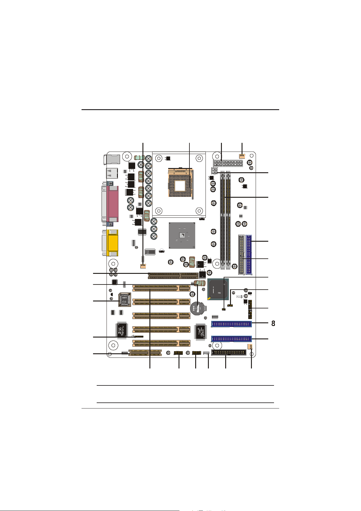
2.3. Mainboard Layout
Introduction
11
22
23
13
12
TS
R
PO
RD
&
A
KB1
O
SE
U
O
EYB
M
K
/2
/2
PS
PS
USB1
TS
R
PO
SB
U
COM1
RTS
O
&
P
L
IA
LLEL
SER
A
PAR
&
-IN
TS
IC
R
O
UT, M
IP
ID
E-O
E/M
M
,LIN
A
G
E-IN
LIN
AUDIO1
AUDIO CODEC
2M FLASHEPROM
I/OCHIPSET
19
UM7 70045
0149
95020 2CF
T014.3
18
FAN1
CPUFAN
AG P
PCI 1
PCI 2
PCI 3
PCI 4
IR
C
PCI 5
CNR
1220
ATX P OWER
ATX1
JP10
6030L
ET
EB
C
C
B6030L
CE
CET
R
JP9
WOL
ATX 12 V POW ER
R
intel
SECERT
FW82801DB
L140IZ6Q
QC68ES
M C
INTEL '01
G135988VI D
140 KOREA
JP11
BID E2
BID E1
IR
FLP FLOPP Y
DIM2DIM1
JP12
FAN2
JP5
LOTES
USB2 USB1
JP4
'01
M
C
L148A320
RET
82SEC
QC
ES
KE
RG88B
RAIDCHIPSET
C
JP5
FAN2
FAN
YS
S
3
4
5
6
IDE1IDE2
16
17
R
TO
EC
N
ON
C
EL
18
PAN
T
N
RO
F
JP14
7
FA
N
3
14 14 15
910
Note: Because of optional items and design changes, your mainboard
may not be identical to the one shown in the illustration.
Mainboard Layout
21
9
Page 16

Mainboard Users Manual
Key to Mainboard Components
No. Name Function
1mPGA478
2ATX1ATX Pentium 4 standard power connector
3JP10
4DIM1~2
5IDE1
6IDE2IDE 2 connector
7BIDE1
8BIDE2
9 FLP
10 PCI1~5 32-bit PCI slots
11 AGP
12 CNR
13 JP12 IrDA compliant Infrared (IR) connector
14 JP4~5 Front USB port
15 JP9
16 JP11
17 JP12 Clear CMOS
18 JP14
19 FAN1
20 FAN2
21 FAN3 AGP/chipset fan connector
22 BTY
23
CPU socket
ATX 12V power connector
DD R SDRAM Memory module slots
IDE 1 connector
RAID 1 connector
RAID 2 connector
Floppy drive connector
Accelerated Gra phics Port (AGP) slot
Communi c ati ons Ne tworki ng Rise r
Wake on LA N connector
EXT-SMI Switch
Front Panel connector
CPU fan connector
System fan connector
RTC b attery
Flash BIOS
10
Mainboard Layout
Page 17

2.4. Microprocessor
The mainboard is designed to operate with the following processor:
Processor Type Speed FSB
Intel Pentium 4 1.4~2.4GHz 400/ 533MHz
An onboard switching voltage regulator provides the required 1.05 to
1.825 volts for the processor. The processor sends five VID (Voltage
Identification) signals to the switching voltage regulator. The switching regulator generates the correct voltage for the processor.
2.5. CPU Packaging
The mainboards CPU socket is a surface mount, mPGA478B type ZIF
(Zero Insertion Force) socket. The socket has 478 pins with 50 mil pin
pitch.
Note: ZIF sockets are sockets designed for easy insertion of pin grid
array (PGA) chips. The chip is dropped into the socket,
and a lever is used to secure the chip in place.
Introduction
2.6. AC 97 Codec
This mainboard features the AC 97 codec. The AC 97 Audio codec is
compliant with the AC 97 2.1 specification, and supports 18-bit ADC
(Analog Digital Converter) and DAC (Digital Analog Converter)
resolution as well as 18-bit stereo full-duplex codec with independent
and variable sampling rates. Further features include support for four
analog line-level stereo inputs.
11Microprocessor
Page 18

Mainboard Users Manual
2.7. Chipset
The P8F151 supports the Intel 845 chipset. The Intel 845 chipset is optimized for the Pentium 4 processor, and incorporates NetBurst microarchitecture.
NetBurst architecture doubles the instruction pipeline to 20 stages, runs
the ALU (Arithmetic Logic Unit) at twice the core frequency and improves performance in the Level 1 and 2 caches.
The 845 chipset consists of two controller hubs, the 82845 Memory
Controller Hub (MCH) and the 82801DB I/O Controller Hub (ICH2):
u The 82845 Memory Controller Hub supports a 266 MHz bus clock,
PC1600/PC2100 SDRAM memory, and the 4xAGP interface.
u The 82801DB I/O Controller Hub provides direct connection to
graphics and memory components for faster access to peripherals and
provides the features and bandwidth required for high performance
PCs.
In addition to future application support, the 845 chipset was designed
with the following features:
u Advanced packaging technology and industry leading electrical
design innovations ensure long-term system reliability over wide
operating conditions.
u The AGP4X interface providing the most advanced graphics
support available, enabling graphics bandwidth of over 1 GB/s.
u Two USB controllers provide high performance peripherals
with 480 Mbps of bandwidth, while enabling support for up
to four USB ports.
u AC 97 implementation delivers six channels of audio for
enhanced sound quality and full surround sound capability.
u Dual Ultra ATA/100 controllers support faster IDE transfers to storage
devices.
12
Chipset
Page 19

2.8. RAID (Optional)
Bus mastering design allows utilization of a RAID (Redundant Array of
Independent Disks). A RAID is a set of two or more hard disks and a
specialized disk controller, which controls the RAID function. Using a
RAID, the user can write and read to more than one disk at the same time,
that is, complete data duplication can be achieved, or, excess data can ve
transferred to another disk. the problems of disk failure are minimized with
the use of a RAID.
This concludes Chapter 2. Chapter 3 covers hardware installation.
Introduction
RAID
13
Page 20

Mainboard Users Manual
3. Hardware Installation
This chapter explains how to use your mainboard to build a powerful
computer system. At a minimum, you will need the following components
in order to build a fully functioning system.
r Computer case with P4 standard ATX power supply
r mPGA478B Processor
r One DDR SDRAM memory module
r One floppy disk drive
r One UDMA-66/100 IDE hard disk drive
r One CD-ROM drive
r One display monitor
r One mouse
r One PS/2 keyboard
r One set of loudspeakers
Of course, you can use the system I/O ports and expansion slots to add
many more features and components to your system than the items listed
above.
3.1. Unpacking
The P8F151 mainboard package contains the following items:
u One mainboard
u One IDE 66/100 40-pin ribbon cable
u One floppy 34-pin ribbon cable
u Driver and utility CD
u Users manual reference
After removing the mainboard from its anti-static bag, place it on a
grounded or antistatic surface (component side up). Inspect the mainboard
and contact your vendor immediately if it is damaged.
14
Unpacking
Page 21

Hardware Installation
3.2. Installation
The P8F151 is designed to fit into a standard ATX form factor chassis.
The pattern of the mounting holes and the position of the back panel
connectors meet the ATX system board specification. The chassis comes
with various mounting fasteners, which are made of metal or plastic. It is
highly recommended to use as many metal fasteners as possible to mount
the mainboard in the chassis for better grounding.
To install the mainboard you need to install the CPU and DIMM memory
modules, attach the connectors, and set the correct CPU speed in the
CMOS setup.
3.3. Safety Measures
Computer components and electronic circuit boards can be damaged by
discharges of static electricity. Working on computers that are still
connected to a power supply can be extremely dangerous. Follow the
simple guidelines below to avoid damaging your computer:
u Always disconnect the mainboard from the ATX power supply, and
disconnect the computer from the power outlet whenever you are
working inside the computer case.
Installation
u If possible, wear a grounded wrist strap when you are installing
the mainboard or working inside the computer case. Alternatively,
discharge any static electricity by touching the bare metal chassis
of the computer case, or the bare metal body of any other grounded
appliance.
u Hold electronic circuit boards by the edges only. Do not touch the
components on the board unless it is necessary to do so. Do not
flex or stress the circuit board.
u Leave each component inside the static-proof packaging that it
ships with until you are ready to use the component for the
installation.
15
Page 22
Mainboard Users Manual
3.4. Connector/Jumper Location
RTS
PO
RD
&
A
KB1
USE
O
M
KEYBO
PS/2
PS/2
USB1
&
IAL
SER
RTS
PO
USB
COM1
RTS
PO
ALLEL
PAR
LOTES
FAN2
ATX P OWE R
ATX 1
JP10
ATX 12V POWER
FAN
SYS
16
&
IC-IN
TS
T, M
IPOR
ID
E/M
,LINE-OU
AM
G
LIN E -IN
AUDIO 1
AUDIO C ODEC
PCI1
2M FLASHEPROM
PCI2
PCI3
I /O C HI PS ET
PCI4
C
PCI5
CNR
IR
CPU FAN
U M77 00 45
0149
950202CF
T
014.318
FAN1
AGP
M
C
'01
320
L148A
T
CRE
82SE
C
Q
EES
G88BK
R
USB2 USB1
JP4
JP5
L
T
6030
E
EB
C
C
RAID CHIPSET
C
030L
EB6
C
CET
BIDE2
R
BIDE1
JP9
WOL
DIM2DIM 1
R
intel
SECERT
FW82 801DB
L140 IZ6Q
QC68E S
M C
INTEL ' 01
G135 988VI D
140 KORE A
JP11
JP5
IR
FLP FLOPPY
IDE1IDE2
R
JP12
FAN 2
ECTO
ONN
C
PAN EL
T
FRON
JP14
FAN3
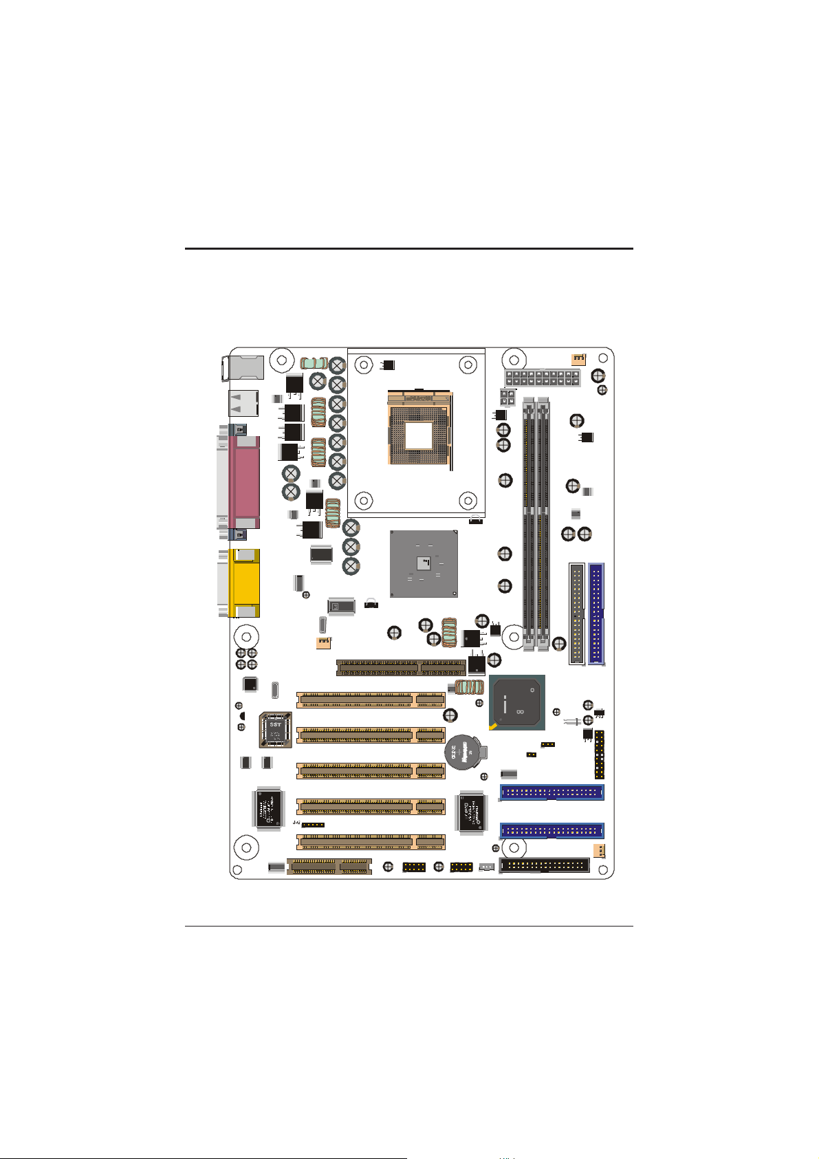
Connector/Jumper Location
Page 23
(
)
Hardware Installation
3.5. Attaching Connectors
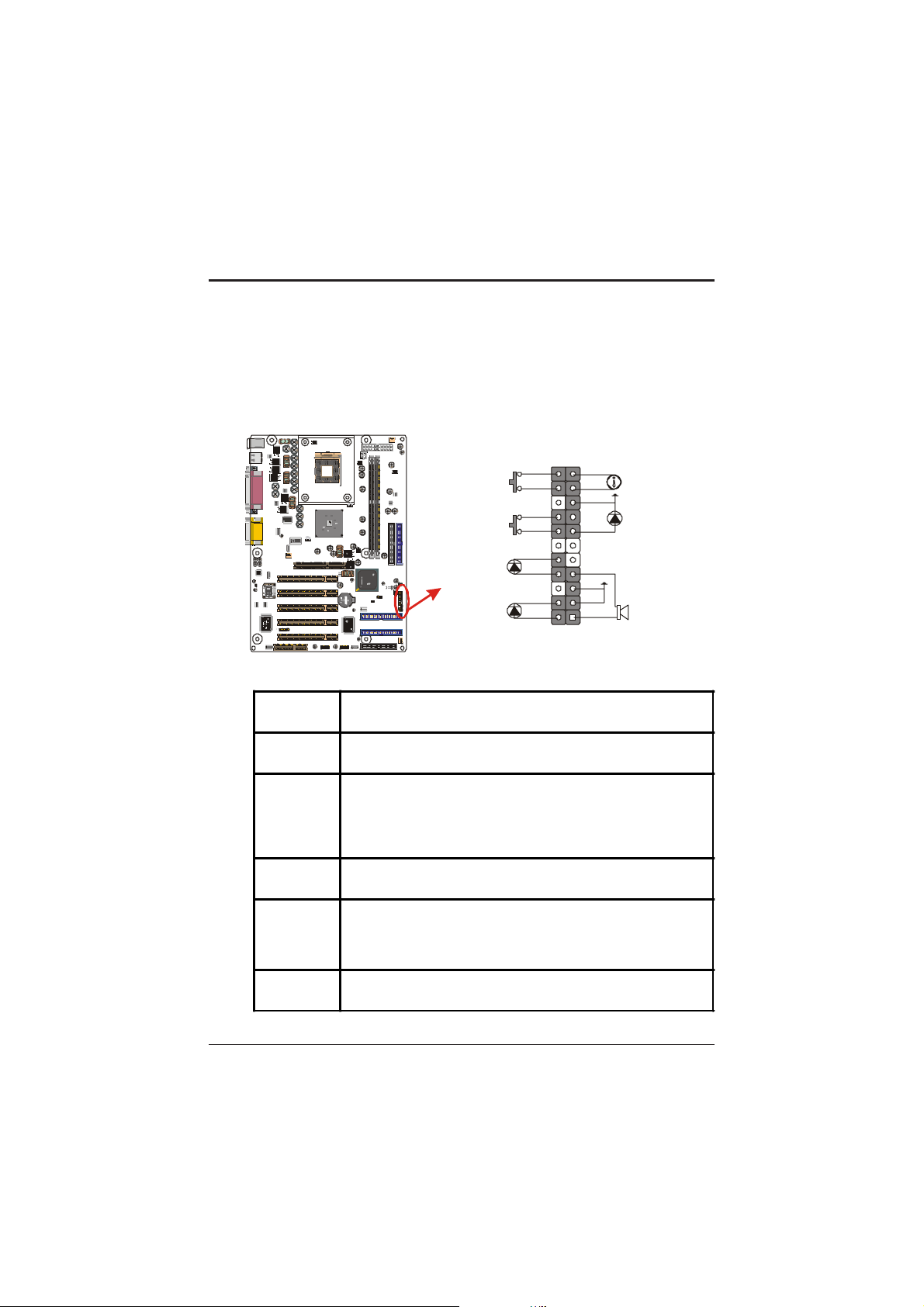
3.5.1. Front Panel Connectors (JP14)
There are seven connectors on the mainboard for speaker, switches, and
indicator lights on the systems front panel.
KB1
USB1
COM1
UM770045
0149950202CF
T014.318
AUDIO1
FAN1
CPUFAN
AGP
PCI1
AUDIOCODEC
2MFLASH EPROM
PCI2
PCI3
I/OC HIPSET
PCI4
IR
C
PCI5
CNR
PWSW
RESET
STBLED
HDDLED
PWRLED
& keylock
SPEAKER
FAN2
ATX POWER
SYSFAN
ATX1
JP10
'01MC
QC82SECRETL148A320
RG88BKEES
USB2 U SB1
ATX 12VPOW ER
(PWSW)
POWER SWI TCH
(Re set)
RESET BUTTON
CET
CEB6030L
DIM2DIM1
CEB6030L
CET
intel
R
SECERT
FW82801DB
L140IZ6Q
QC68ES
INTEL ' 01
MC
G135988VID
140KOREA
JP12
JP11
RAIDCHIPSET
TECHNOLOGY,I NC.
PROMISE
C
PDC20265R
2000-0111
BIDE2
R
FAN2
BIDE1
JP5
JP9
IR
WOL
FLP FLOP PYJP5
(STB LED)
IDE1IDE2
STANDBY LED
(HDD LED)
FRONT PANELC ONNECTOR
JP14
HDD LED
FAN3
Ground
Power on/of f
Ground
Reset Single
LED ca tho de
LED ano de
LED ca tho de
LED ano de
Pin1
Ground
Keyb oard
LED ca tho de
Non
LED ano de
+5V
Ground
Non
Spea ke r-o ut
LOTE S
JP4
This 2-pin connector connects to the case-mounted
Power button.
This 2-pin connector connects to the case-mounted
reset switch and is used to reboot the system.
This 2-pin connector connects to the case-mounted
Standby LED to indicate a standby status. The LED
remains lit even when the system is off to indicate
that AC power is available. When the system enters
standby mode, the LED starts blinking.
This 2-pin connector connects to the case-mounted
HDD LED to indicate hard disk activity.
This 5-pin connector connects to the case-mounted
keylock switch and the power LED. The keylock
switch is used to lock the keyboard for security
purposes.
This 4-pin connector connects to the case-mounted
speaker.
PWRLED& keylock
POWER LED
&KEYLOCK
SPEAKER
Attaching Connectors
17
Page 24
Mainboard Users Manual
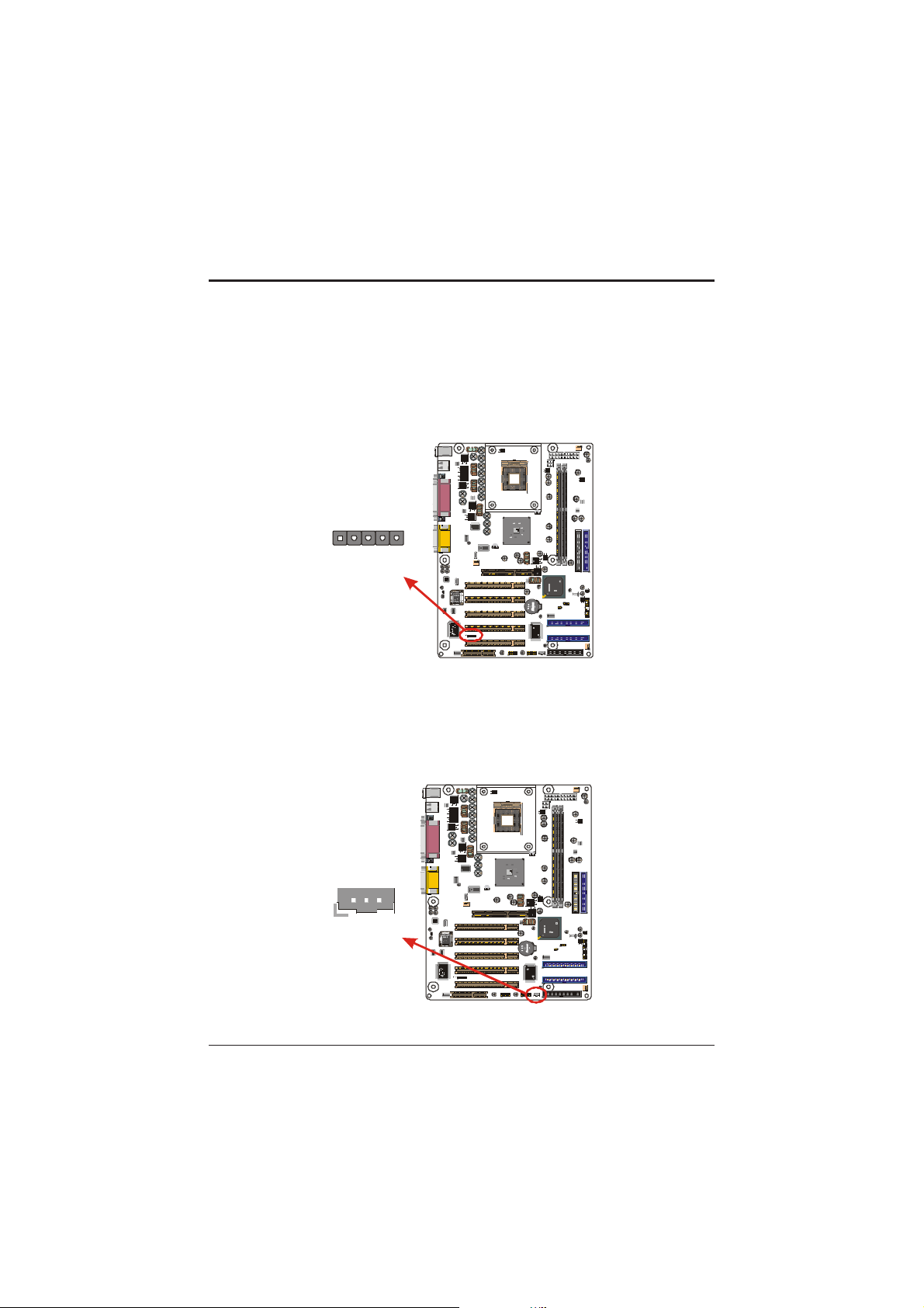
3.5.2. Infrared (IR) Connector (JP2)
This 5-pin headers connects to an optional wireless transmitting and
receiving infrared module via a cable and a bracket. Configure BIOS to
enable the IrDA port if you attach an infrared module to this connector.
Refer to Integrated Peripherals in Chapter 4 for details.
FAN2
FAN
S
ATX POWER
SY
ATX1
JP10
ATX 12VPOW ER
CEB6030L
CET
DIM2DIM1
CEB
6030L
CET
IDE1IDE2
intel
R
SECERT
FW82801DB
L140IZ6Q
QC68ES
INTEL ' 01
MC
G135988VID
140KOREA
R
TO
C
JP12
NE
ON
JP11
LC
NE
PA
NT
O
FR
TECHNO
C
PD
PR
2000-
C20265R
O
011
LOGY,IN
MISE
1
C.
JP14
BIDE2
R
FAN2
BIDE1
FAN
3
JP5
JP9
IR
WOL
FLP FLOP PYJP5
Pin 1
KB1
USB1
COM1
X
X
C
D
R
R
N
VC
G
IR
CIR
AUDIO1
TX
IR
AUDIOCODEC
2MFLASH EPROM
I/OCHIPSET
C
LOTE S
'01
M
C
L148A320
QC82
SECRET
RG8 8BKEES
UM770045
0149
950202CF
T014
.318
FAN1
CPUFAN
AGP
PCI1
PCI2
PCI3
PCI4
IR
PCI5
CNR
USB2 U SB1
JP4
RAIDCHIPSET
3.5.3. LAN/Modem Wake up Connectors (JP9)
These 3-pin headers are used for remote wake up of the computer through
a network or modem signal.
FAN2
FAN
S
ATXPOWER
SY
ATX1
JP10
ATX 12V POWER
030L
CEB6
CET
DIM2DIM1
CEB6030L
T
CE
TEC
PD
PR
C
HN
2000-
C20265R
O
OLOG Y,IN
011
MISE
1
R
C.
JP9
WOL
IDE1IDE2
intel
R
SECERT
FW82801DB
L140IZ6Q
QC68ES
INTEL '01
MC
G135988VID
140KOREA
OR
T
EC
JP12
N
ON
JP11
C
NEL
PA
NT
O
FR
JP14
BIDE2
FAN2
BIDE1
FLP FL OPPYJP5
FAN
3
JP5
IR
Pin 1
WOL
KB1
USB1
COM1
AUDIO1
AUDIO CODEC
2MFLASHEPROM
I/OCHIPSET
C
LOT ES
'01
M
C
L148A320
QC82SECRET
RG8 8BKEES
UM770045
0149
950202CF
T01
4.3
18
FAN1
CPUFAN
AGP
PCI1
PCI2
PCI3
PCI4
IR
PCI5
CNR
USB2 USB1
JP4
RAIDCHIPSET
18
Attaching Connectors
Page 25
Hardware Installation
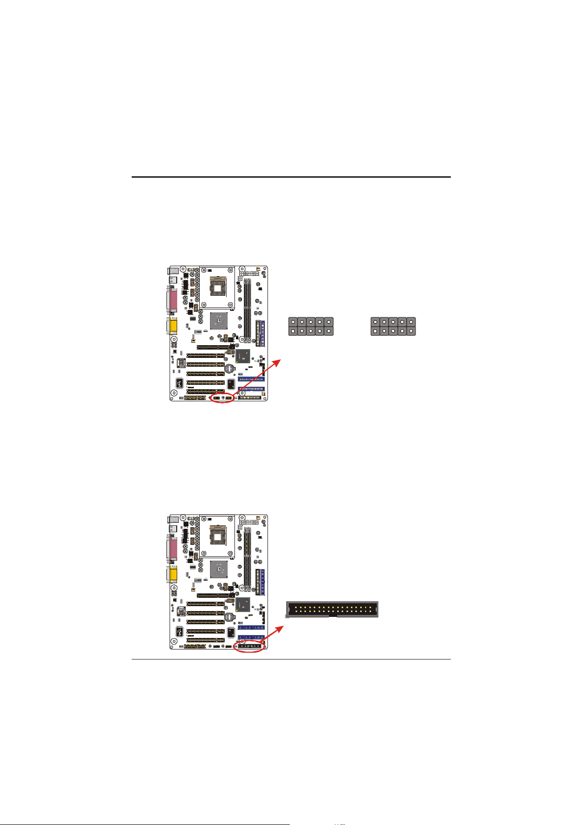
3.5.4. Front USB Header (JP4,JP5)
The mainboard provides oen onboard 10-pin of dual USB port (port 3 and
port 4) headers. The headers on the same signal with USB port 1 and port 2
on the back panel.
KB1
USB1
COM1
LOTE S
FAN2
FAN
YS
ATX POWER
S
ATX1
JP10
ATX 12VPOW ER
USB Port 4 USB Port 6
D
D
C
-
+
N
N
G
G
VC
D
'01
M
C
L148A320
QC8
2SECRET
RG88BKEES
UM770045
0149
950202CF
T014.318
AUDIO1
FAN1
CPUFAN
AGP
PCI1
AUDIOCODEC
2MFLASH EPROM
PCI2
PCI3
I/OCHIPSET
PCI4
IR
C
PCI5
CNR
ET
CEB6030L
C
CEB6
030L
CET
intel
SECERT
FW82801DB
L140IZ6Q
QC68ES
INTEL ' 01
MC
G135988VID
140KOREA
JP11
RAIDCHIPSET
TEC
C
PDC
2000
PR
HNOLO
BIDE2
OMISE
2026
-0111
GY,IN
5R
C.
R
BIDE1
USB2
USB1
JP9
IR
WOL
JP4
JP5
FLP FLOP PY
Pin 1 Pin 1
DIM2DIM1
IDE1IDE2
R
R
TO
EC
JP12
NN
CO
L
E
AN
TP
ON
FR
JP14
FAN2
FA
N3
JP5
D
JP4 JP5
-
+
C
D
D
D
N
N
D
VC
G
G
USB Port 3 USB Port 5
D
D
C
-
+
N
N
G
G
VC
D
D
-
+
C
D
D
D
N
N
D
VC
G
G
3.5.5. Floppy Drive Connector (FLOPPY)
A floppy disk drive ribbon cable has two connectors to support two
floppy disk drives. The connector with twisted wires always connects to
drive A; the connector with untwisted wires connects to drive B. You
must orient the cable connector so that the pin 1 (color) edge of the cable
corresponds with pin 1 of the I/O port connector.
KB1
USB1
COM1
LOTE S
FAN2
FAN
YS
ATX POWER
S
ATX1
JP10
ATX 12VPOW ER
UM770045
0149950202CF
T014.31
AUDIO1
8
FAN1
CPUFAN
AGP
PCI1
AUDIOCODEC
2MFLASH EPROM
PCI2
PCI3
I/OCHIPSET
PCI4
IR
C
PCI5
CNR
USB2 USB1
JP4
Attaching Connectors
'01
M
C
L1 48A320
QC82SECRET
RG 88BKEES
6030L
CET
CEB
DIM2DIM1
CEB6
030L
CET
IDE1IDE2
intel
R
SECERT
FW82801DB
L140IZ6Q
QC68ES
INTEL ' 01
MC
G135988VID
140KOREA
OR
CT
JP12
NNE
O
JP11
LC
E
PAN
NT
RO
F
RAIDCHIPSET
TEC
C
PD
PR
HNOLO
2000-
C202
O
0111
MIS
GY,IN
65R
E
R
C.
JP14
BIDE2
FAN2
BIDE1
JP9
WOL
FAN
3
JP5
IR
FLP FLO PPYJP5
FLOPPYPIN1
19
Page 26
Mainboard Users Manual
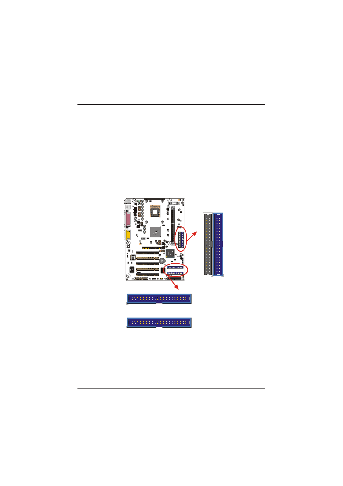
3.5.6. IDE Connectors (IDE1,IDE2,BIDE1,BIDE2)
An IDE drive ribbon cable has two connectors to support four IDE drives.
If a ribbon cable connects to two IDE drives at the same time, one of them
has to be configured as Master and the other has to be configured as
Slave by setting the drive select jumpers on the drive.
Consult the documentation that came with your IDE drive for details on
jumper locations and settings. You must orient the cable connector so that
the pin 1 (color) edge of the cable corresponds to pin 1 of the I/O port
connector.
Pin 1
Pin 1
KB1
USB1
COM1
AUDIO1
AUDIOCODEC
2MFLA SHEPR OM
I/OCHIPSET
C
LOTE S
'01
M
C
L148A320
QC82SECR ET
RG88BKE ES
UM 770045
0149
950202CF
T014.318
FAN1
CPUFAN
AGP
PCI1
PCI2
PCI3
PCI4
IR
PCI5
CNR
USB2 USB1
JP4
RAID CHIPSE T
FAN2
FAN
S
ATX POW ER
SY
ATX1
JP10
ATX 12V POWE R
IDE2 IDE1
ET
CEB6030L
C
DIM2DIM1
CEB
6030L
CET
IDE1IDE2
intel
R
SECERT
FW82801DB
L140IZ6Q
QC68ES
MC
INTEL'01
G135988VID
140KOREA
OR
CT
JP12
NE
ON
JP11
C
EL
PAN
T
N
RO
F
TEC
C
PR
H
PD
200
NOLOG
C202
OMISE
0-0
65R
111
Y,IN
R
C.
JP9
WOL
JP14
BIDE2
FAN2
BIDE1
F
AN
3
JP5
IR
FLP FLOPPYJP5
Pin 1Pin 1
BIDE2
FA N2
BIDE1
20
Attaching Connectors
Page 27
Hardware Installation
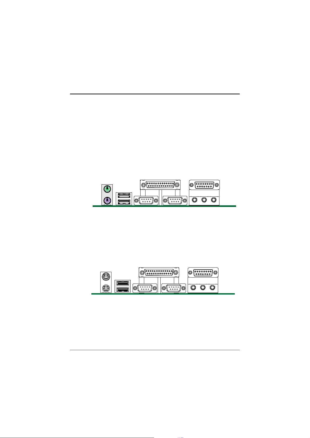
3.5.7. Back Panel Connectors
The back panel provides external access to PS/2 style keyboard and
mouse connectors, two serial ports, one parallel port, dual USB ports, and
audio Line-out, Line-in, Mic-in, game/midi ports which are integrated on
the mainboard. The figures below show the location of the back panel I/O
connectors.
PS/2 Mouse and PS/2 Keyboard Ports
Connect a PS/2 mouse to the green 6-pin mini DIN connector. The system
will automatically assign IRQ 12 to the PS/2 mouse if one is connected.
PS /2 Mo us e por t
PS /2 Key boa rd po rt
Connect a PS/2 keyboard to the purple 6-pin mini DIN connector. If you
want to connect a standard AT size (large DIN) connector, you must use
an adapter.
Universal Serial Bus Ports
You can connect two USB devices or USB hubs to the USB ports.
USB ports
The USB ports provide a hardware interface for low-speed peripherals
such as the keyboard, mouse, joystick, scanner, printer and telephony
devices, and also support MPEG-1 and MPEG-2 digital video. The USB
ports have a maximum bandwidth of 480 Mbits/sec (equivalent to 60
Mbytes/sec), and up to 127 devices can be attached. Fast devices can use
the full bandwidth, while lower-speed ones can transfer data using a 60
Mbytes/sec sub-channel.
Attaching Connectors
21
Page 28
Mainboard Users Manual
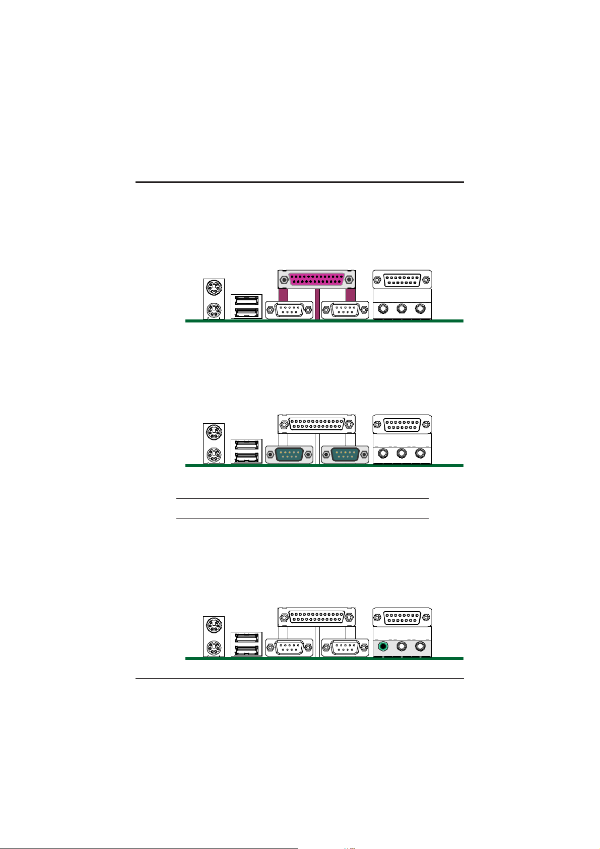
Parallel Port
Connect a printer or other parallel device to the burgundy-colored 25-pin
parallel port. You can set the parallel port IRQ and parallel port mode in
BIOS. Refer to Integrated Peripherals in Chapter 4 for details.
Parallel p ort
Serial Port
Connect a serial device such as a mouse or modem to the turquoise 9-pin
serial port. You can set the serial port IRQs in BIOS. Refer to Integrated
Peripherals in Chapter 4 for details.
COM1 port
COM2 port
Note: Serial printers must be connected to the serial port.
Audio Line-Out Port
You can connect various audio devices to this audio jacks. Connect
headphones or powered speakers to the lime-colored lineout connector.
Line-Out port
22
Attaching Connectors
Page 29
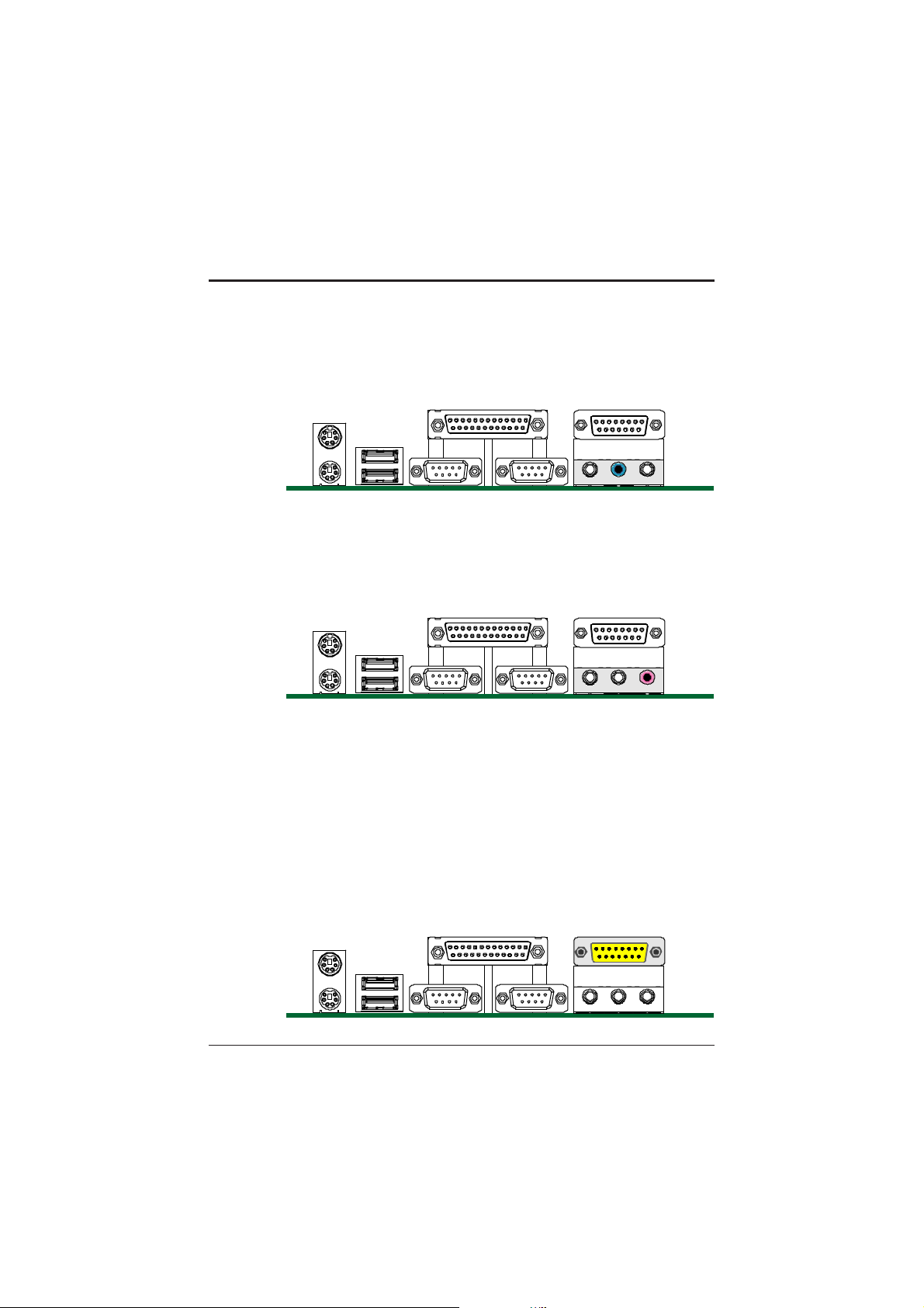
Line-In port
Hardware Installation
Audio Line-In Port
You can connect a tape player or another audio source to the light blue
Line-in connector to record audio on your computer or to play audio
through your computers sound chip and speakers.
Audio Mic-In Port
You can connect a microphone to the pink microphone connector to
record audio to your computer.
Mic-In port
You can also connect to the pink microphone, blue and green Line-out
connector to connect ALC-650 (optional) chip. The software by ALC in
driver controls Mic-in, Line-in or 5.1channel audio.
Audio MIDI/GAME Port
You can connect a joystick, game pad, or other game device to the
gold 15-pin game port. You can also connect a MIDI device for playing or
editing audio.
MIDI/G AME port
Attaching Connectors
23
Page 30
Mainboard Users Manual
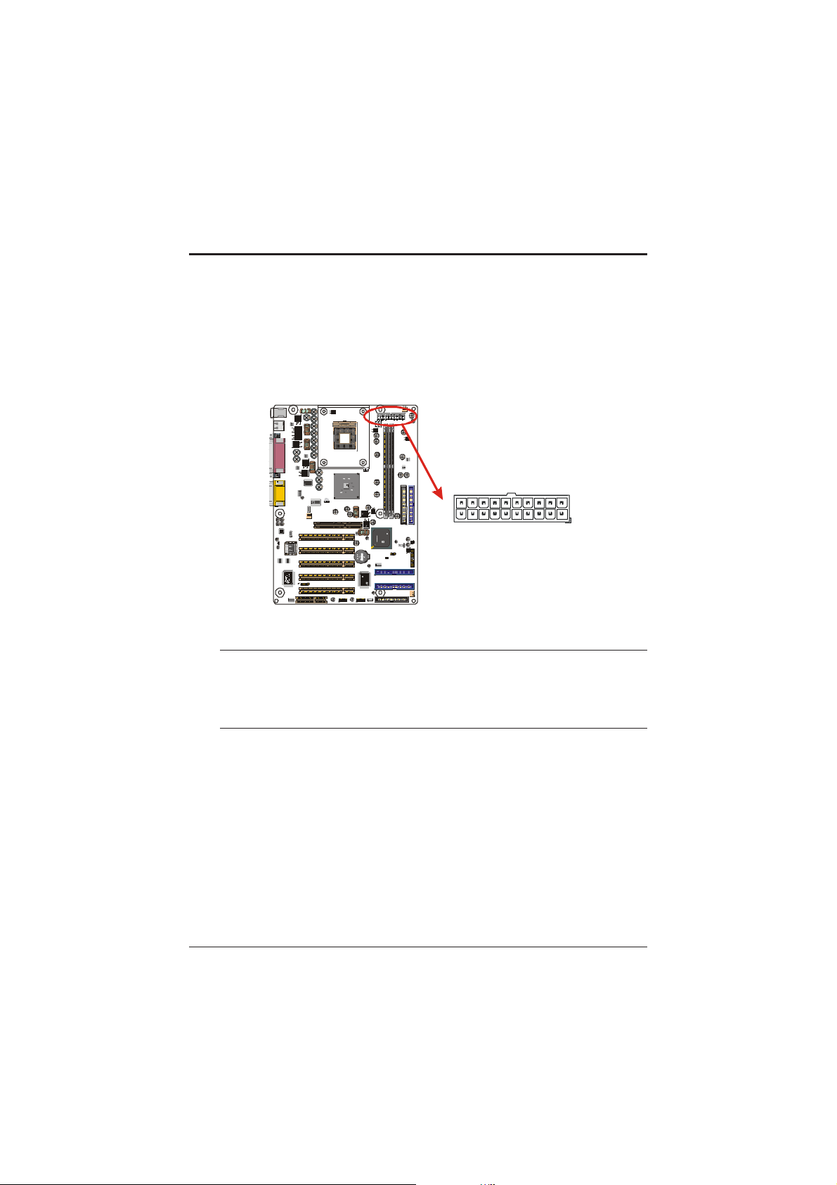
3.5.8. Power Supply Connector (ATX1)
The ATX power supply has a single lead connector with a clip on one side
of the plastic housing. There is only one way to plug the lead into the ATX
power connector. Press the lead connector down until the clip snaps into
place and secures the lead onto the connector.
KB1
USB1
COM1
AUDIO1
AUDIOCODEC
2MFLA SHEPR OM
I/OCHIPSET
C
LOTE S
'01
M
C
L1 48A320
QC82SECRET
RG88BKEES
UM 770045
0149
950202CF
T014.318
FAN1
CPUFAN
AGP
PCI1
PCI2
PCI3
PCI4
IR
PCI5
CNR
RAID CHIPSE T
USB1
USB2
JP4
FAN2
FAN
S
ATX POW ER
SY
ATX1
JP10
ATX 12V POWE R
n
O
er Su ppl y
D
D
D
N
C
N
G
+5V
+5V
T
CEB6030L
CE
DIM2DIM1
CEB6030L
ET
C
TECHNO
C
PD
PR
2000-
C202
O
011
LOGY,IN
MISE
65R
1
C.
R
IDE1IDE2
intel
R
SECERT
FW82801DB
L140IZ6Q
QC68ES
INTEL'01
MC
G135988VID
140KOREA
R
TO
C
JP12
NE
ON
JP11
C
EL
AN
TP
N
RO
F
JP14
BIDE2
FAN2
BIDE1
JP9
WOL
FA
N3
JP5
IR
FLP FLOPPYJP 5
D
N
ood
G
-12V
Stan dby
erG
ow
P
+5V
D
N
N
N
ow
G
G
P
+3.3V
G
-12V
Pin 1
D
D
N
N
+5V
+5V
G
G
+3.3V
+3.3V
Warning: Incorrect installation of the power supply could result in serious
damage to the mainboard and connected peripherals. Make sure
the power supply is unplugged from the AC outlet before
connecting the leads from the power supply.
24
Attaching Connectors
Page 31
Hardware Installation
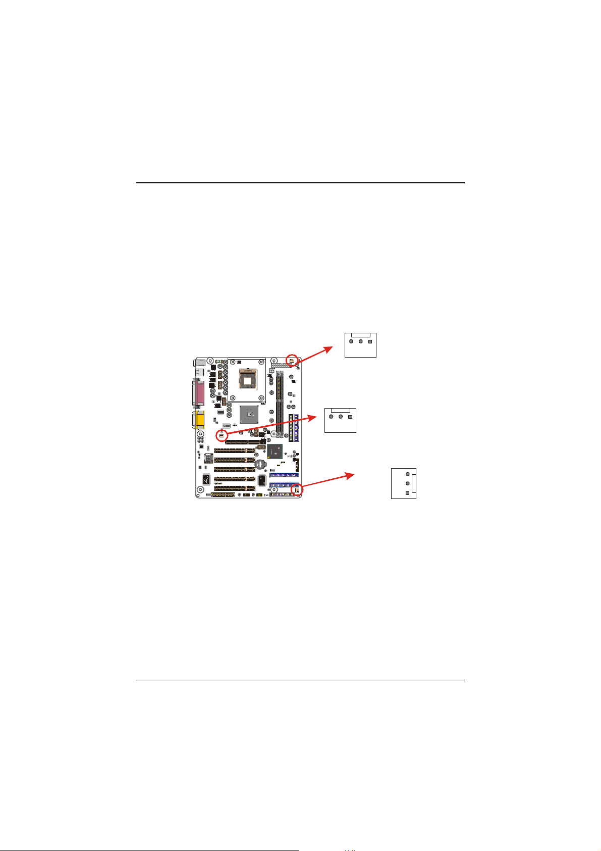
3.5.9. CPU/AGP/System Fan Power Supplies
FAN1/ FAN2/FAN3
There are three fan connectors on the mainboard for the cooling fans. The
connectors support fans of 12V DC/500mAMP (six watt) or less. When
the system goes into sleep state, fans should be shut down to eliminate
audible noise and reduce power consumption. You can monitor the fan
speed by way of the 82845E chip (providing the fan comes with a tachometer output).
AGP FAN (FAN2 )
Pin 1
KB1
USB1
COM1
LOT ES
FAN2
ATX POWER
SYSFAN
ATX1
JP10
ATX12VPOWER
GND
Spee d/RPM
+12V
CPU F AN (FAN1 )
Speed /RPM
GND
+12V
Pin 1
Syst emFAN(FAN 3)
Spee d/ RPM
+12V
GND
Pin 1
'01MC
L148A320
RG88BKEESQC82SECR ET
UM 770045
0149
950202CF
T014.318
AUDIO1
FAN1
CPUFAN
AGP
PCI1
AUDIOCODEC
2MFLASH EPROM
PCI2
PCI3
I/OCHIPSET
PCI4
IR
C
PCI5
CNR
USB2 USB1
JP4
CEB6030L
CET
DIM2DIM1
CEB6030L
CET
RAIDCHIPSET
TECHNOLOGY,INC.
PROMISE
C
PDC20265R
2000-011 1
R
JP9
WOL
JP5
intel
SECERT
FW82801DB
L140IZ6Q
QC68ES
INTEL '01
G135988VID
140KOREA
BIDE2
BIDE1
FLP FLOPPY
IDE1IDE2
R
MC
JP12
JP11
FRONT PANELC ONNECTOR
JP14
FAN2
FAN3
JP5
IR
Attaching Connectors
25
Page 32
Mainboard Users Manual
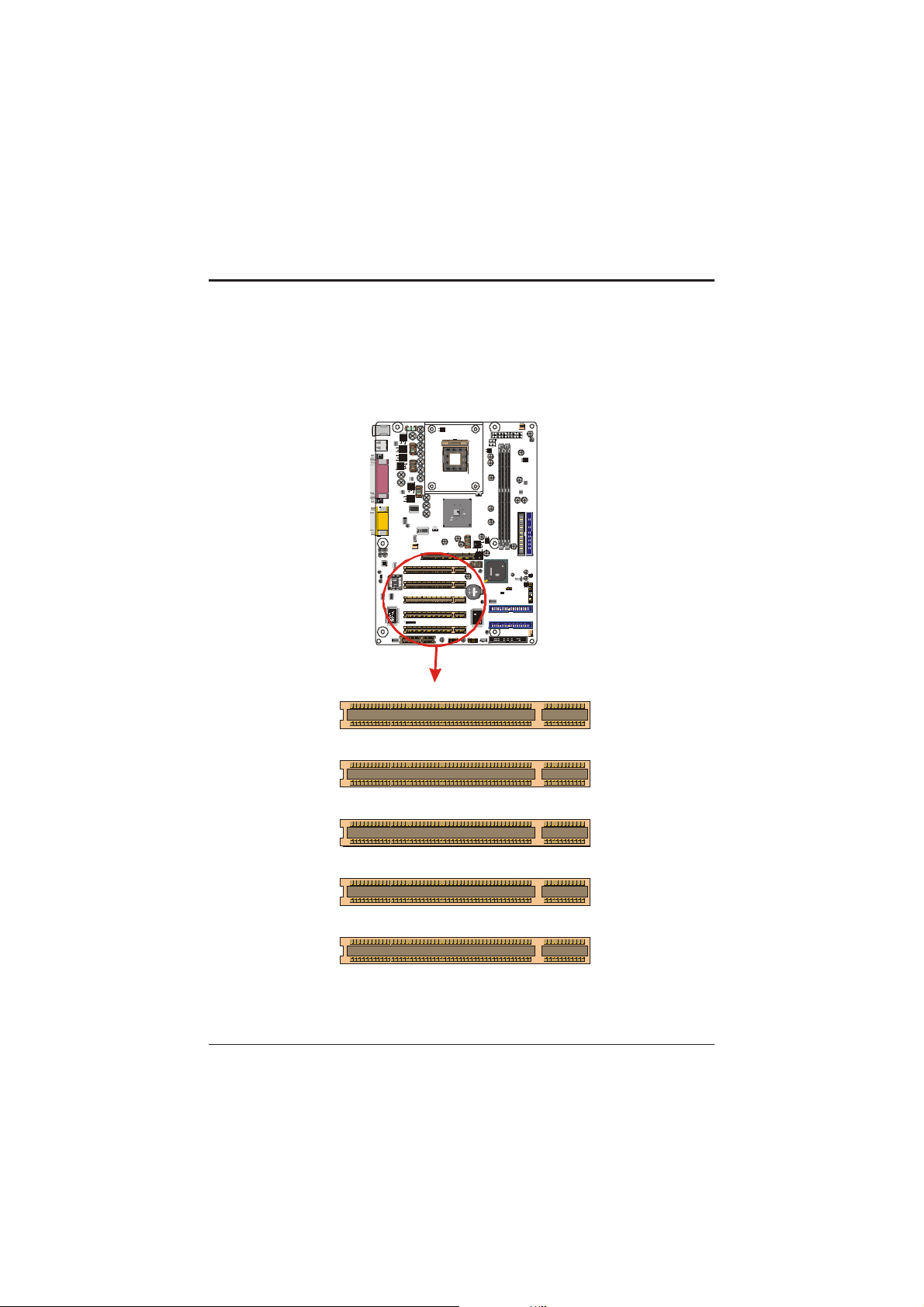
3.5.10. PCI Connector (PCI1~PCI5)
PCI connector is one of equipment interfaces that connects pheripheral
equipment and motherboard. Its transfer speed is faster than traditional
ISA. PCI is the mainstream transfer interface for extra adopter.
PCI
PC2
PC3
PC4
Pin 1
Pin 1
Pin 1
Pin 1
KB1
USB1
COM1
AUDIO1
AUDIOCODEC
2MFLA SHEPR OM
I/OCHIPSET
C
LOTE S
'01
M
C
L148A320
QC8
2SECRET
RG8
8BKEES
UM770045
0149950202CF
T014.318
FAN1
CPUFAN
AGP
PCI1
PCI2
PCI3
PCI4
IR
PCI5
CNR
USB2 U SB1
JP4
RAIDCH IPS ET
JP5
FAN2
FAN
S
ATX POW ER
Y
S
ATX1
JP10
ATX12VPOWER
CEB6030L
CET
DIM2DIM1
CEB6030L
CET
TEC
C
PD
PR
HNOLO
2000-
C20265R
OM
011
GY,IN
ISE
1
C.
R
JP9
WOL
intel
SECERT
FW82801DB
L140IZ6Q
QC68ES
INTEL '01
G135988VID
140KOREA
BIDE2
BIDE1
FLP FLOPPY
IDE1IDE2
R
MC
OR
CT
JP12
NE
N
JP11
CO
EL
AN
P
NT
O
FR
JP14
FAN2
FA
N
3
JP5
IR
Pin 1
PC5
26 Attaching Connectors
Page 33
Hardware Installation
3.6. Installing the CPU
3.6.1. Before You Begin
1. Be sure that your processor kit includes the following items:
u One processor with the fan or heat sink attached
u One power cable (for CPU with cooling fan attached)
2. Place the mainboard on a workbench (not in a chassis). Be sure that
the mainboard is empty (that is, no DIMMs, cables, or cards are
installed) and that the holes for the fan or heat sink support pegs are
empty.
3.6.2. Installation Procedure
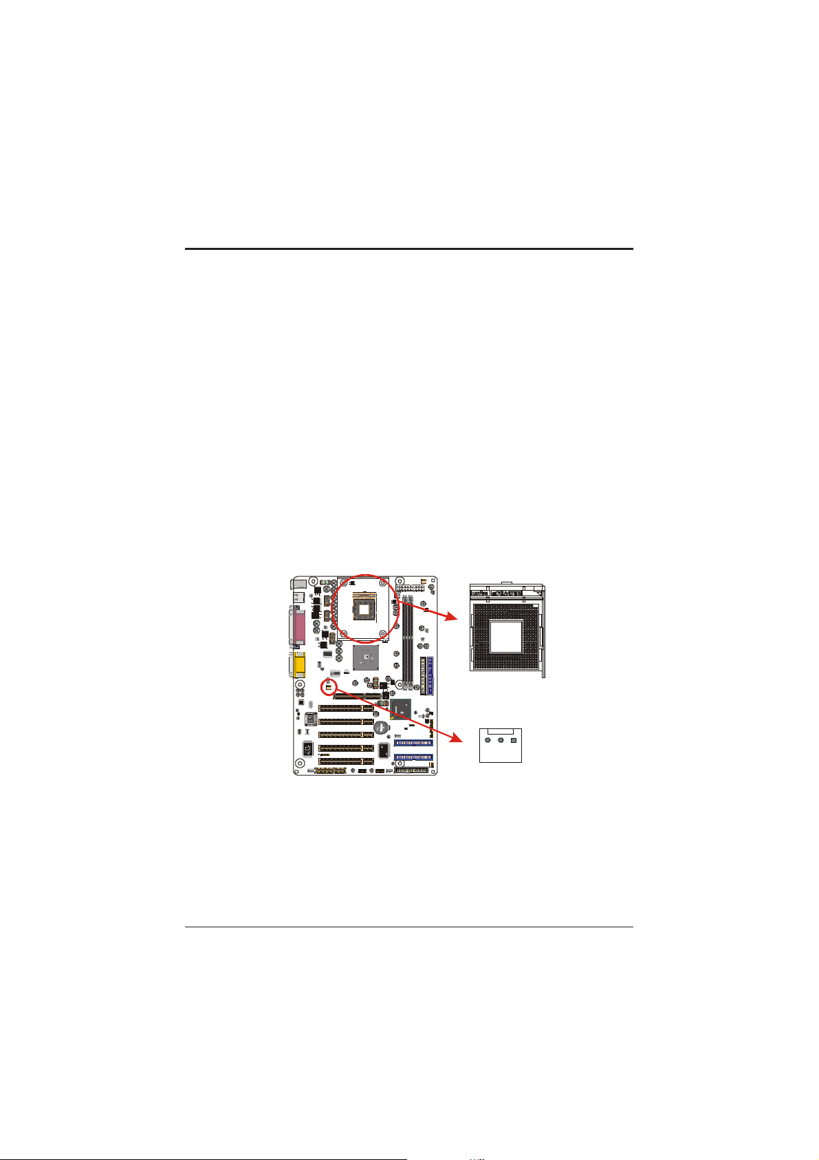
1. On the motherboard, identify the CPU Socket 478 and the cooling fan
power supply connector CPU FAN.
FAN2
KB1
USB1
COM1
LOT ES
N
FA
S
ATX POW ER
SY
ATX1
JP10
ATX12VPOWER
CPU SOCKET4 78
'01
M
C
L148A320
QC82SECRET
RG8 8BKEES
UM770045
0149
950202CF
T014.318
AUDIO1
FAN1
CPUFAN
AGP
PCI1
AUDIOCODEC
2MFLA SHEPR OM
PCI2
PCI3
I/OCHIPSET
PCI4
IR
C
PCI5
CNR
USB2 USB1
JP4
CEB6030L
CET
DIM2DIM1
CEB6030L
CET
RAIDCH IPS ET
TEC
C
PR
HNOLO
PD
2000-
O
C202
MISE
0111
G
65R
Y,IN
R
C.
WOL
JP5
BIDE2
BIDE1
JP9
intel
SECERT
FW82801DB
L140IZ6Q
QC68ES
INTEL '01
M C
G135988VID
140KOREA
FLP FLOPPY
IDE1IDE2
R
CPU FAN Pow er Su pply
OR
CT
JP12
NE
N
JP11
CO
L
NE
PA
NT
O
FR
JP14
FAN2
F
AN
3
JP5
IR
Pin 1
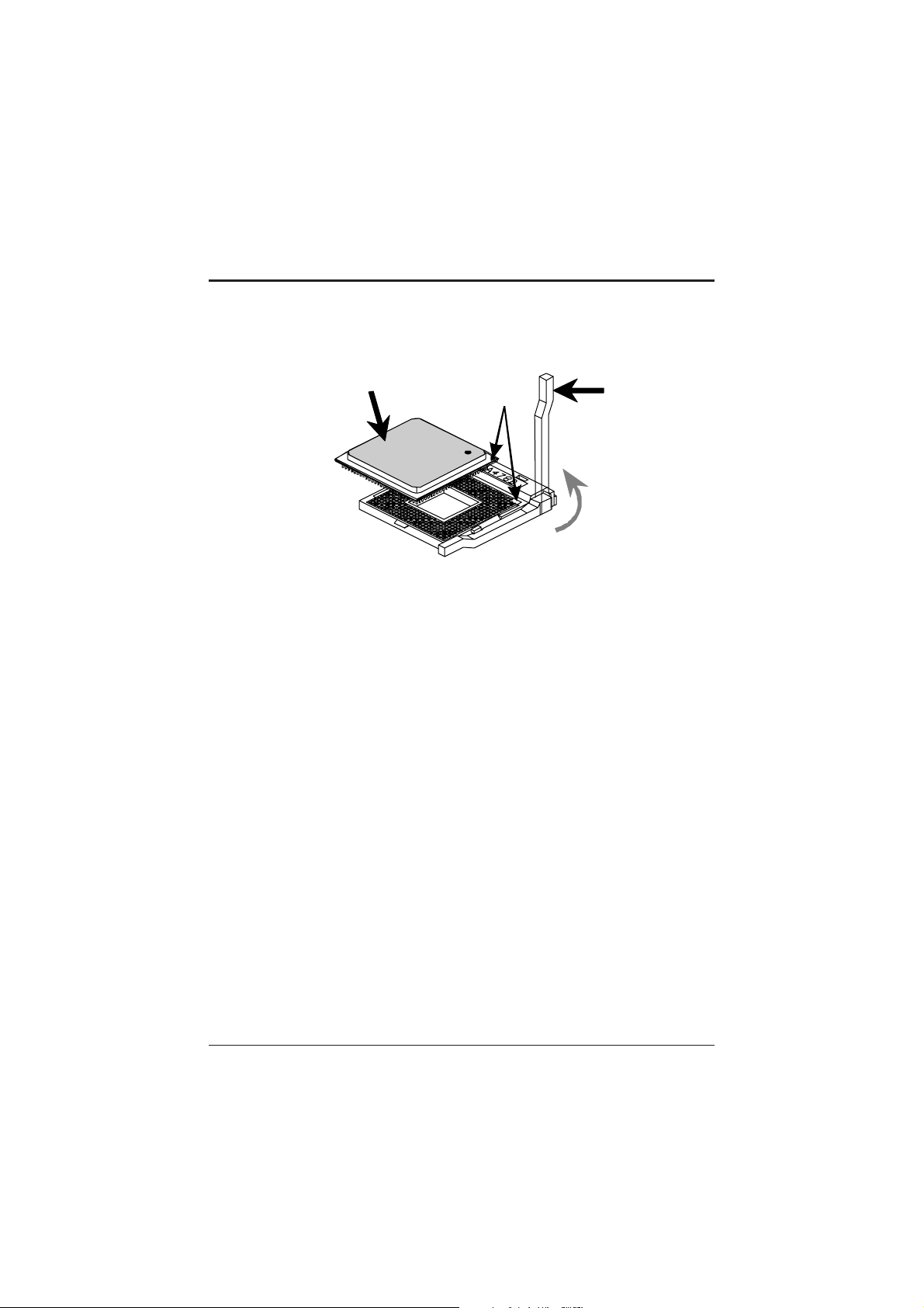
2. Push the CPU socket lever slightly to the side and then raise it as far as
it can go.
3. Identify the pin-1 corner of the PGA478. The pin-1 corner is on the
same side as the locking lever, as shown in the illustration below.
4. Identify the pin-1 corner of the processor (the pin-1 corner on the
processor has a beveled edge).
5. Align the pin-1 corners and drop the processor into the PGA478. The
Installing the CPU
27
Page 34
Mainboard Users Manual
g
processor should drop into place without any force. If it doesnt seat
properly, check that you have the pin-1 corner in the correct position.
CPU Processor
pin 1
Socket Lever
Up to 90 de
ree
6. Swing the locking lever down to lock the processor in place and latch
the lever under the catch on the side of the socket.
7. Plug the cable from the heat sink/cooling fan assembly into the
processor cooling fan power supply CPU FAN.
8. Configuration of the processor is carried out using the system setup
utility as described in Chapter 4. Configure the processor the first time
you turn on the assembled computer.
3.6.3. Removing the Processor
First, remove the mainboard from the chassis. To remove the processor
from the mainboard, follow these steps:
1. Disconnect the fan power cable from the mainboard.
2. Push the CPU socket lever slightly to the side and then raise it as
far as it can go. You will feel a resistance as the processor is freed
from the socket.
3. Remove the processor.
28
Installing the CPU
Page 35
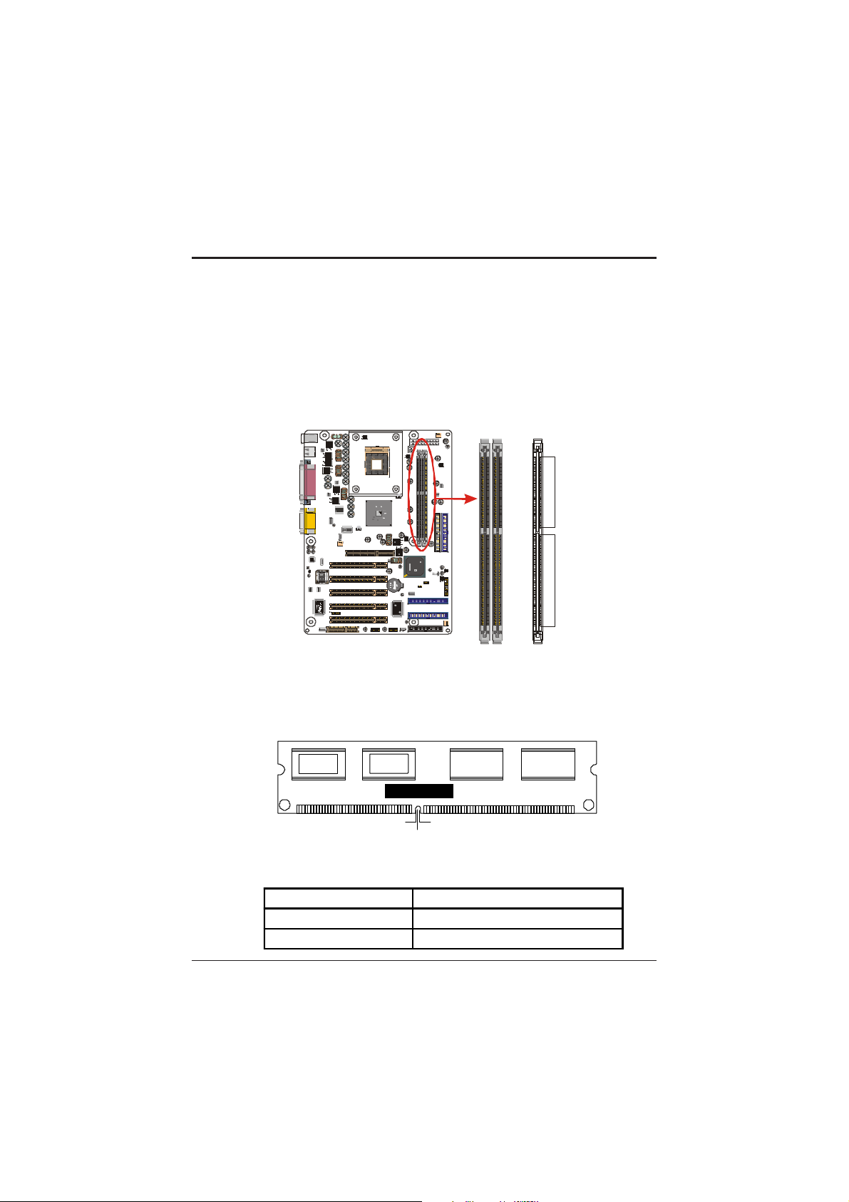
Bank 0 (DIMM1) 64MB/128MB/512MB/1GB
Bank 1 (DIMM2) 64MB/128MB/512MB/1GB
Total S ystem Memory 64MB ~ 2GB
Hardware Installation
3.7. Installing System Memory
Maximum system memory supported by the mainboard is 2 GB.
The mainboard has two DIMM Sockets. Memory can be installed using
184-pin DDR SDRAM DIMM memory modules. There are no jumper
settings required for the memory size or type, which is automatically
detected by the BIOS.
FAN2
KB1
USB1
COM1
AUDIO1
AUDIOCODEC
2MFLA SHEPR OM
I/OCHIPSET
C
LOTE S
M
C
'01
L148A320
QC8
2SECRET
RG88BKEES
UM770045
0149
950202CF
T014
.31
8
FAN1
CPUFAN
AGP
PCI1
PCI2
PCI3
PCI4
IR
PCI5
CNR
USB2 U SB1
JP4
6030L
CET
CEB
CEB6
030L
CET
RAIDCH IPSE T
TECHN
C
PD
PR
2000-0
C2026
O
OLO
MISE
111
5R
GY,IN
C.
R
WOL
N
DIMM1 DIMM2
FA
YS
ATX POW ER
S
ATX1
JP10
ATX12VPOWER
DIM2DIM1
IDE1IDE2
intel
R
SECERT
FW82801DB
L140IZ6Q
QC68ES
MC
INTEL '01
G135988VID
140KOREA
R
TO
EC
JP12
N
ON
JP11
C
EL
PAN
T
N
O
FR
JP14
BIDE2
FAN2
BIDE1
JP9
F
AN
3
JP5
IR
FLP FLOPPYJP5
Lock
Lock
pins
80
pins
104
You must use 2.5V unbuffered DIMMs in the mainboard. To determine the
DIMM type, check the notches on the DIMMs.
184-pin DIMM
Voltage key position
5.0V Reserved
2.5V
Install the 184-pin DDR SDRAM modules in any combination as follows:
Installing the CPU
29
Page 36
Mainboard Users Manual
3.8. Setting Jumpers
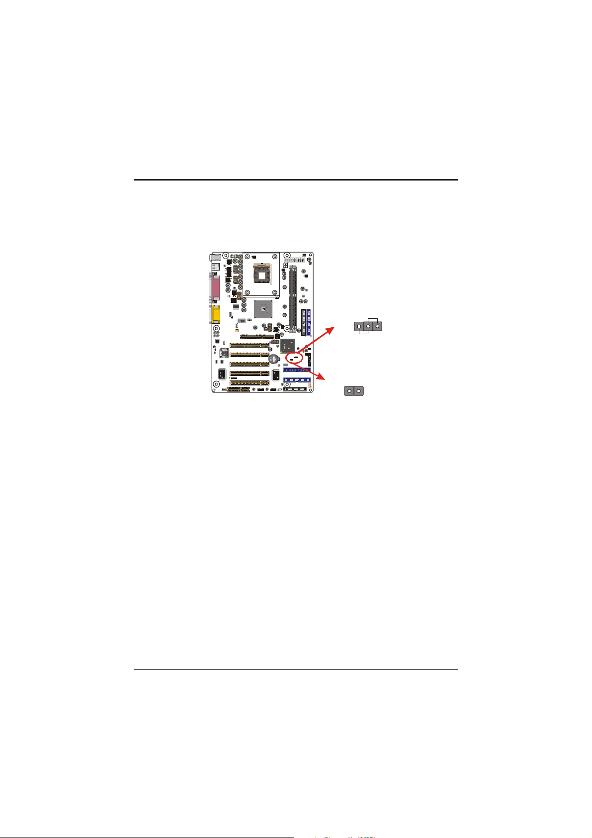
Refer to the following illustration and instructions to set the jumpers on
your mainboard.
KB1
USB1
COM1
AUDIO1
AUDIOCODEC
2MFLA SHEPROM
I/OCHIPSET
C
LOTE S
'01
M
C
L148A320
QC82SECR ET
RG88BKE ES
UM770045
0149
950202CF
T014
.31
8
FAN1
CPUFAN
AGP
PCI1
PCI2
PCI3
PCI4
IR
PCI5
CNR
USB2 USB1
JP4
RAID CHIPSET
JP5
FAN2
FAN
S
ATX POW ER
SY
ATX1
JP10
ATX 12V POWER
Clea r CMO S Set ting s
CEB6030L
CET
DIM2DIM1
CEB6
030L
CET
TEC
C
PD
PR
HNOLO
2000-
O
C202
MISE
0111
G
65R
Y,IN
R
C.
BIDE2
BIDE1
JP9
WOL
intel
SECERT
FW82801DB
L140IZ6Q
QC68ES
INTEL'01
MC
G135988VID
140KOREA
IR
FLP FLOPPY
IDE1IDE2
R
R
CTO
JP12
E
NN
JP11
CO
EL
PAN
T
N
RO
F
JP14
FA
N3
Ext- SMI Switch
Pin 1
FAN2
JP5
Pin 1
JP11
JP12
N
orm
al
C
lear C
M
O
S
Clear CMOS Jumper (JP12)
You may need to clear the CMOS if your system cannot boot up because
you forgot your password, the CPU clock setup is incorrect, or the CMOS
settings need to be reset to default values after the system BIOS has been
updated.
Refer to the following solutions to reset your CMOS setting:
Solution A
1. Power off the system and disconnect the power cable.
2. Place a shunt to short pin 2 and pin 3 of JP12 for five seconds.
3. Place the shunt back to pin 1 and pin 2 of JP12.
4. Power on the system.
30
Installing the CPU
Page 37

Hardware Installation
Solution B
If the CPU clock setup is incorrect, you may not be able to boot up. In this
case, follow these instructions:
1. Turn the system off, then on again. The CPU will automatically
boot up using standard parameters.
2. As the system boots, enter BIOS and set up the CPU clock.
Note: If you are unable to enter BIOS setup, turn the system on and off a
few times.
Ext-SMI Switch (JP11)
When you press the button, then the system enter SMI.
3.9. Auto Power On
After losing AC power, the system will not turn on automatically when the
power comes back unless you set the options in BIOS.
This concludes Chapter 3. Chapter 4 covers the BIOS setup program.
Installing the CPU
31
Page 38

Mainboard Users Manual
4. BIOS Configuration
After the hardware configuration of the mainboard is finished, and the
system hardware has been assembled, the system may be powered up. At
this point, CMOS setup should be run to ensure that system information is
correct.
The mainboard employs the latest Award BIOS CMOS chip with support
for Windows Plug and Play. This CMOS chip contains the ROM Setup instructions for configuring the mainboards BIOS. The BIOS (Basic Input
and Output System) Setup program is a menu driven utility that enables you
to make changes to the system configuration and tailor your system to suit
your individual work needs. It is a ROM-based configuration utility that
displays the systems configuration status and provides you with a tool to
set system parameters. These parameters are stored in non-volatile batterybacked-up CMOS RAM that saves this information even when the power is
turned off. When the system is turned back on, the system is configured with
the values found in CMOS.
Using easy-to-use pull down menus, you can configure such items as:
r Hard drives, diskette drives, and peripherals
r Video display type and display options
r Password protection from unauthorized use
r Power management features
The settings made in the Setup program intimately affect how the computer performs. It is important, therefore, first to try to understand all the
Setups options, and second, to make settings appropriate for the way you
use the computer. This chapter provides clear explanations for all Setup
options.
32
BIOS Configuration
Page 39

This program should be executed under the following conditions:
r When changing the system configuration
r When a configuration error is detected by the system and you are
prompted to make changes to the Setup program
r When resetting the system clock
r When setting the CPU clock speed so that it automatically runs
either fast or slow
r When redefining the communication ports to prevent any conflicts
r When making changes to the Power Management configuration
r When changing the password or making other changes to the
security setup
Normally, CMOS setup is needed when the system hardware is not
consistent with the information contained in the CMOS RAM, whenever
the CMOS RAM has lost power, or the system features need to be
changed.
4.1. Entering Setup
When the system is powered on, the BIOS will enter the Power-On Self Test
(POST) routines. These routines perform various diagnostic checks; if an
error is encountered, the error will be reported in one of two different ways:
1. If the error occurs before the display device is initialized, a series
of beeps will be transmitted.
2. If the error occurs after the display device is initialized, the screen
will display the error message.
After the POST routines are completed, the following message appears:
Entering Setup
33
Page 40
Mainboard Users Manual
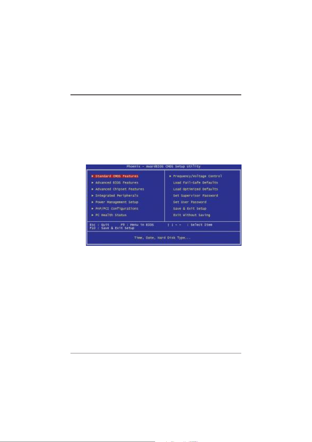
Press DEL to enter SETUP
To access the AWARD BIOS SETUP program, press the <DEL> key to
display the CMOS SETUP UTILITY screen:
These screens provide access to the utilitys various functions.
Listed below are explanations of the keys displayed at the bottom of the
screen:
Key Function
Esc Escape key: Exits the current menu
higf Cursor keys: Scroll through the items on a menu
+/-/PU/PD Plus, minus, Page Up and Page Down keys: Modify the
selected fields values
F10 F10 key: Saves the current configuration and exits setup
F1 F1 key: Displays a screen that explains all key functions
F5 F5 key: Loads previously saved values to CMOS
F6 F6 key: Loads a minimum configuration for troubleshooting.
F7 F7 key: Loads optimum set of values for peak performance
34
Entering Setup
Page 41
BIOS Configuration
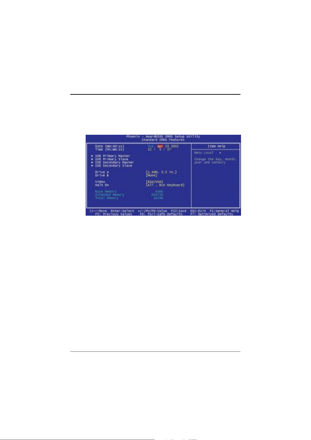
4.2. Standard CMOS Features
Standard CMOS Features is the same for all three chipsets. Selecting
Standard CMOS Features on the main program screen displays the
following menu:
The Standard CMOS Setup utility is similar for all three chipsets and is
used to configure the following features:
Date: Month, Day, Year
Time: Hour, Minute, and Second. Use 24 Hour clock format (for PM
numbers, add 12 to the hour, you would enter 4:30 p.m. As 16:30).
IDE Devices: Your computer has two IDE channels (Primary and
Secondary) and each channel can be installed with one or two devices
(Master and Slave). Use these items to configure each device on the IDE
channel. Press Enter to display the IDE sub-menu:
u IDE HDD Auto-Detection: Press <Enter> while this item is high
lighted if you want the Setup Utility to automatically detect and
configure a hard disk drive on the IDE channel.
If your system has an IDE hard drive, you can use this utility to
detect its parameters and enter them into the Standard CMOS
Setup automatically.
Standard CMOS Setup
35
Page 42

Mainboard Users Manual
If the auto-detected parameters displayed do not match the ones
that should be used for your hard drive, do not accept them. Press
the <N> key to reject the values and enter the correct ones manually
in the Standard CMOS Setup screen.
Note: If you are setting up a new hard disk drive that supports
LBA mode, more than one line will appear in the param
eter box. Choose the line that lists LBA for an LBA drive.
Do not choose Large or Normal if the hard disk drive is
already fully formatted when you installed it. Select the mode that
was used to format it.
u IDE Primary/Secondary Master/Slave: If you leave this item
at Auto, the system will automatically detect and configure
any IDE devices it finds. If it fails to find a hard disk, change
the value to Manual and then manually configure the drive
by entering the characteristics of the drive in the items below
(Capacity, Cylinder, Head, Precomp, etc.). Refer to your
drives documentation or look on the drive if you need to
obtain this information. If no device is installed, change the
value to None.
u Access Mode: This item defines some special ways that can be
used to access IDE hard disks such as LBA (Large Block
Addressing). Leave this value at Auto and the system will
automatically decide the fastest way to access the hard disk
drive.
Press <Esc> to close the IDE device sub-menu and return to the
Standard CMOS Features page.
Drive A and Drive B: Select the type of floppy disk drive installed in
your system. The options are:
u 360K, 5.25 in
u 1.2M, 5.25in
u 720K, 3.5in
36
Standard CMOS Setup
Page 43

BIOS Configuration
u 1.44M, 3.5in (Driver A default)
u 2.88M, 3.5in
u None (Not Installed) (Drive B default).
The Not Installed option could be used as an option for diskless
workstations.
Video: Set this field to the type of graphics card installed in your system.
If you are using a VGA or higher resolution card, choose the EGA/VGA
option. The options are:
u MONO
u CGA 40
u CGA 80
u EGA/VGA (default).
Halt On: This setting determines which type of errors will cause the
system to halt during bootup. The options are:
u All Errors (default)
u No Errors
u All
u But Keyboard
u All, But Diskette
u All, But Disk/Key.
Base/Extended/Total Memory: These items are automatically detected by
the system at start up time. These are display only fields. You cannot make
changes to these fields.
After you have made your selections in the Standard CMOS Setup screen,
press <ESC> to go back to the main screen.
Standard CMOS Setup
37
Page 44
Mainboard Users Manual
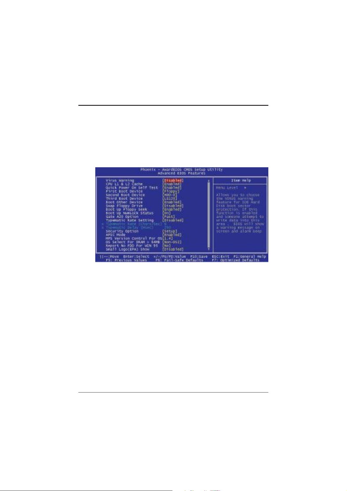
4.3. Advanced BIOS Features
Selecting Advanced BIOS Features on the main program screen
displays this menu, which allows you to define advanced information
about your system. You can make modifications to most of these items
without introducing fatal errors to your system. Note that the page has a
scroll-bar to scroll down to more items.
The following explains the options for each feature:
Virus Warning: When enabled, any attempt to write to the boot sector or
partition table will halt the system and cause a warning message to appear.
If this happens, you can use an anti-virus utility on a virus free, bootable
floppy diskette to reboot and clean your system. The default setting is
Disabled.
CPU L1 & L2 Cache: These settings enable the CPU internal (L1) and
external (L2) cache. Enabling these items provides better performance.
The default setting is Enabled.
Quick Power On Self Test: This will skip some diagnostic checks during
the Power On Self Test (POST) to speed up the booting process. The
default setting is Enabled.
38
Advanced BIOS Features
Page 45

BIOS Configuration
First/Second/Third Boot Device: Use these three items to select the priority
and order of the devices that your system searches for an op-erating system
at start-up time. The default settings are Floppy, HDD-0, or LS120
respectively.
Boot Other Device: If you enable this item, the system will search all
other possible locations for an operating system if it fails to find one in the
devices specified under the First, Second, and Third boot devices. The
default setting is Enabled.
Swap Floppy Drive: If you have two floppy diskette drives in your
system, this item allows you to swap the assigned drive letters so that
drive A becomes drive B, and drive B becomes drive A. The default
setting is Disabled.
Boot Up Floppy Seek: If this item is enabled, it checks the geometry of
the floppy disk drives at start-up time. You dont need to enable this item
unless you have an old diskette drive with 360K capacity. The default
setting is Enabled.
Boot Up Numlock Status: If set to Off, the cursor controls will
function on the numeric keypad. The default setting is On.
Gate A20 Option: This option accesses memory above 1 MB using the
fast gate A20 line when set to Fast (default). The other option is
Normal.
Typematic Rate Setting: If set to Enabled, enables you to set the
Typematic Rate and Typematic Delay. The default setting is Disabled.
u Typematic Rate (Chars/Sec): This setting controls the speed at
which the system registers repeated keystrokes. The choices range
from 6 to 30 Chars/Sec. The default setting is 6 Chars/Sec.
u Typematic Delay (Msec): This setting controls the time between
the display of the first and second characters. There are four delay
choices: 250ms, 500ms, 750ms and 1000ms. The default setting is
250 ms.
Security Option: This setting controls the password feature. The options
are Setup and System. Selecting Setup will protect the configuration
settings from being tampered with. Select System if you want to use the
Advanced BIOS Features
39
Page 46

Mainboard Users Manual
password feature every time the system boots up. The default setting is
Setup. You can create your password by using the SUPERVISOR/USER
PASSWORD utility in the main program screen.
APIC Mode: Enables or disables APIC (Advanced Programmable
Interrupt Controller) mode. APIC provides symmetric multiprocessing
(SMP) for systems, allowing support for up to 60 processors.
MPS Version Control For OS: Selects the operating system multiprocessor support version. The default setting is 1.4.
OS Select For DRAM > 64MB: Set to OS2 if the system memory size
is greater than 64 MB and the operating system is OS/2. The default
setting is Non-OS2.
Report No FDD For WIN 95: If you are running a system with no floppy
drive and using Windows 95, select Yes for this item to ensure compatibility with the Windows 95 logo certification. Otherwise, select No.
The default setting is No.
Small Logo (EPA) Show: Enables and disables the EPA logo when
booting up. The default setting is Disabled.
After you have made your selections in the BIOS Features Setup screen,
press <ESC> to go back to the main screen.
40
Advanced BIOS Features
Page 47
BIOS Configuration
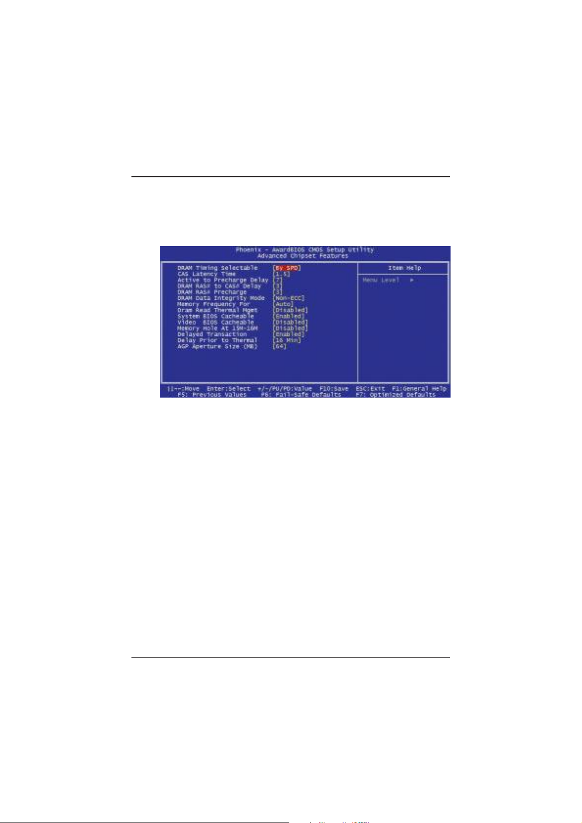
4.4. Advanced Chipset Features
Selecting Advanced Chipset Features on the main program screen
displays this menu:
This screen controls the settings for the boards chipset. All entries
related to the DRAM timing on the screen are automatically configured.
Do not make any changes unless you are familiar with the chipset.
DRAM Timing Selectable: Enables you to set the DRAM timing manually, or automatically using SPD (Serial Presence Detect). SPD is an
EEPROM chip on the memory module that stores information about the
memory chips it contains, including size, speed, voltage, row and column
addresses, and manufacturer. We recommend setting this field to By SPD.
CAS Latency Time: This item enables you to optimize the speed at
which data is accessed in a column by defining CAS latency time. The
CAS latency defines the time delay (in CLKs) before SDRAM starts a
read command after receiving it. Because reading data in a row is twice as
fast, reducing this number can increase performance at the expense of
stability. We recommend that you leave this item at the default value. The
default setting is 1.5.
Active to Precharge Delay: This item enables you to set the number of
DRAM clocks for TRAS. TRAS indicates the time required for the memory
to restore data and come to a full charge. The default setting is 7.
Advanced Chipset Features
41
Page 48

Mainboard Users Manual
DRAM RAS# to CAS# Delay: Enables you to select the RAS to CAS
delay time in HCLKs of 2/2 or 3/3. The value is set at the factory depending on the DRAM installed. Do not change the values in this field unless
you have changed the specifications of the installed DRAM or the
installed CPU. The default setting is 3.
DRAM RAS# Precharge: DRAM must continually be refreshed or it will
lose its data. Normally, DRAM is refreshed entirely as the result of a
single request. This option allows you to determine the number of CPU
clocks allocated for the Row Address Strobe (RAS) to accumulate its
charge before the DRAM is refreshed. If insufficient time is allowed,
refresh may be incomplete and data lost. The default setting is 3.
DRAM Data Integrity Mode: Set this to ECC (error correcting code
default) or Non-ECC, according to the type of installed DRAM.
The default setting is Non-ECC.
Memory Frequency For: Enables you to set the memory frequency for
the installed memory. Select Auto (default) to enable the system to set
the memory frequency automatically according to the installed DRAM.
The options are PC100, or PC133.
DRAM Read Thermal Mgmt: Enables and disables the DRAM read
thermal management function. The default setting is Disabled.
System/Video BIOS Cacheable: When set to Enabled, the System and
Video BIOS will be cached for faster execution. The default setting is
Enabled or Disabled.
Memory Hole At 15M-16M: If Set to Enabled, when the system memory
size is equal to or greater than 16M bytes, the physical memory address
from 15M to 16M will be passed to PCI or ISA and there will be a 1 MB
hole in your system memory. This option is designed for some OS with
special add-in cards which need 15-16 MB memory space. The default
setting is Disabled.
Delayed Transaction: The chipset has an embedded 32-bit posted write
buffer to support delayed transactions cycles. Select Enabled to support
compliance with PCI specification version 2.1. The default setting is
Enabled.
42
Advanced Chipset Features
Page 49

BIOS Configuration
Delay Prior To Thermal: This item allows you to select the delay time to
enable the Pentium 4 CPU Thermal feature. Enable this feature when using
Windows NT 4.0 to prevent the system from hanging. The default setting is
16Min, and other options are 4Min, 8Min, or 32Min.
AGP Aperture Size (MB): This option determines the effective size of
the AGP Graphic Aperture, where memory-mapped graphic data structures are located. The default setting is 64, and other options are 4,
8, 16, 32, 128, or 256.
After you have made your selections in the Chipset Features Setup screen,
press <ESC> to go back to the main screen.
Advanced Chipset Features
43
Page 50
Mainboard Users Manual
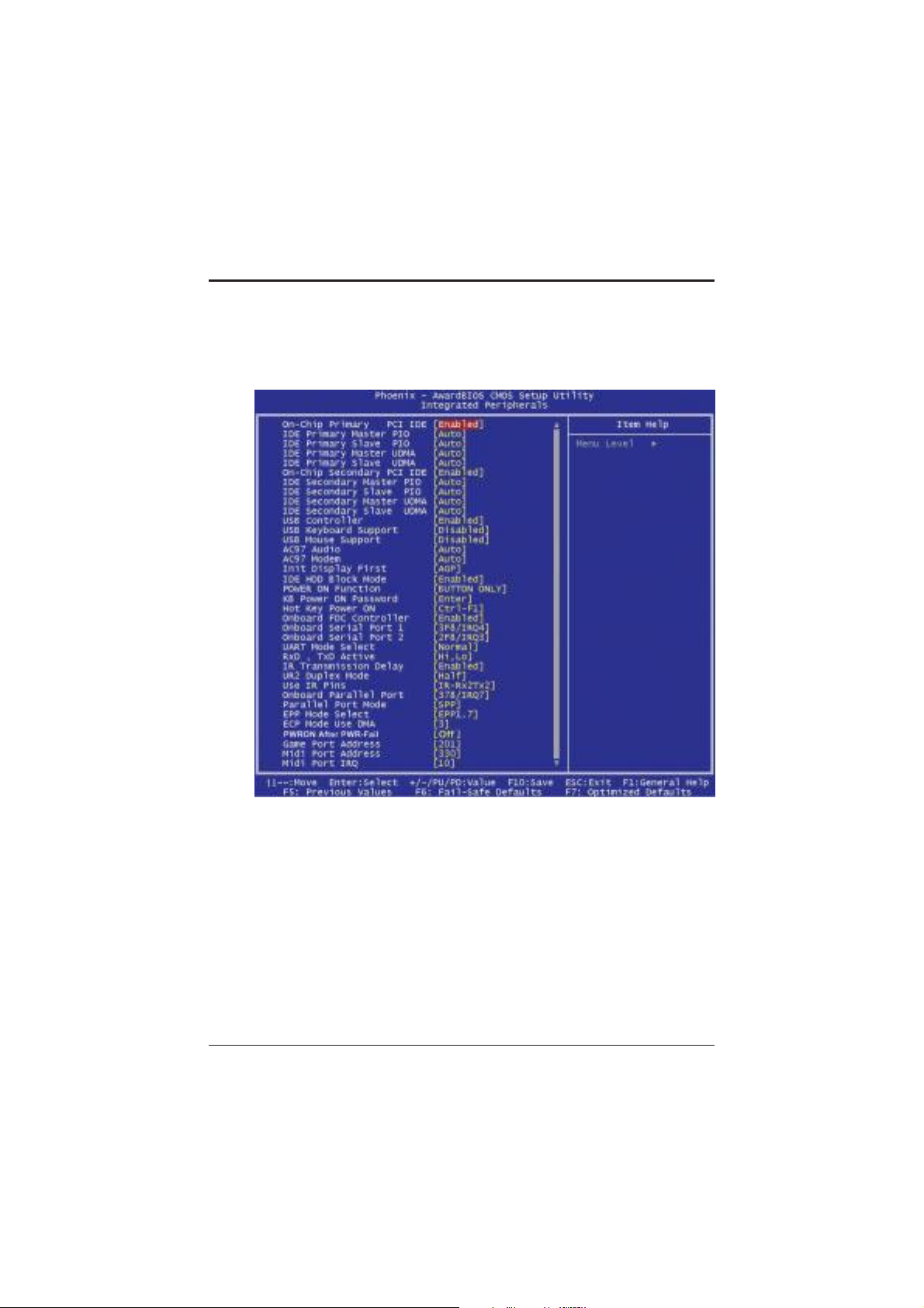
4.5. Integrated Peripherals
Selecting Integrated Peripherals on the main program screen displays
this menu:
OnChip Primary/Secondary PCI IDE: This option enables or disables
theonboard IDE controller. The default setting is Enabled.
IDE Primary/Secondary Master/Slave PIO: When set to Auto the
BIOS will automatically set the mode to match the transfer rate of the hard
disk. If the system wont boot up when set to Auto set it manually to a
lower mode, e.g., from Mode 3 to Mode 2. All IDE drives should work with
PIO mode 0. There are six options: Auto (default), Mode 0, Mode 1,
Mode 2, Mode 3, or Mode 4.
44 Integrated Peripherals
Page 51

BIOS Configuration
IDE Primary/Secondary Master/Slave UDMA: When set to Auto the
BIOS will automatically load the Ultra DMA 33/66/100 driver to match the
transfer rate of IDE hard disk drives that support Ultra DMA 33/66/100
mode. The options are Auto (default) or Disabled.
USB Controller: Enables the USB controller. Leave this at the default
Enabled if you want to connect USB devices to your computer.
USB Keyboard Support: Enables USB keyboard support for legacy
operating systems. The default setting is Disabled.
USB Mouse Support: Enables USB Mouse support for legacy operating
systems. The default setting is Disabled.
AC97 Audio/Modem: Enables or disables the onboard AC 97 audio and
modem chips. The default setting is Auto.
Init Display First: This item sets whether the PCI Slot or AGP is activated
first. The options are PCI Slot or AGP (default).
IDE HDD Block Mode: Enable this field if your IDE hard drive supports
block mode. Block mode enables BIOS to automatically detect the optimal
number of block read and writes per sector that the drive can support. The
default setting is Enabled.
POWER ON Function: Enables you to define actions that will power on
the computer. When set to Button Only (default), the system power can
be turned on by the power button. You can set the mouse and keyboard
activity, and a password to power on the computer from this field.
KB Power ON Password: This field becomes available when you select
Password in the POWER ON Function field. Select this field and press
ENTER. You are prompted to input a password. Type in your password
and press ENTER. You are prompted to confirm your password. Retype
your password and press ENTER. Your password is saved. The next time
you power on your computer, you must type in your password before you
can power the computer on. After you type your password, press and key
or the power button.
Hot Key Power On: Enables you to set the key combination that will
power on the computer. You must enable Hot Key in the Power On
Function field for this item to work.
Integrated Peripherals
45
Page 52

Mainboard Users Manual
Onboard FDC Controller: This option enables the onboard floppy disk
drive controller. The default setting is Enabled.
Onboard Serial Port 1/2: These options are used to assign the I/O
addresses for the two onboard serial ports. The options are: 3F8/ IRQ4
(Port 1 default), 2F8/ IRQ3 (Port 2 default), 3E8/ IRQ4 , 2E8/ IRQ3,
Auto , or Disabled (disables the onboard serial port).
UART Mode Select: Enables you to select the infrared communication
protocol - Normal (default), IrDA, or ASKIR. IrDA is Hewlett Packards
infrared communication protocol with a mazimum baud rate up to 115.2K
bps. ASKIR is Sharps infrared communication protocol with a maximum
baud rate up to 57.6K bps.
RxD, TxD Active: Defines the voltage level for Infrared module RxD
(receive) mode and TxD (transmit) mode. This setting has to match the
requirements of the infrared module used in the system. The options are:
u Hi, Lo (default)
u Lo, Hi
u Lo, Lo
u Hi, Hi
IR Transmission Delay: When set to Enabled, utilizes the capability of
the mainboard to allow faster infrared transmission rates. The option are
Enabled (default), or Disabled.
UR2 Duplex Mode: This field is available when UART 2 Mode is set to
either ASKIR or SCR. This item enables you to determine the infrared (IR)
function of the onboard infrared chip. Full-duplex means that you can
transmit and send information simultaneously. Half duplex (default) is the
transmission of data in both directions, but only one direction at a time.
Use IR Pins: Use this item to set the IR pins. The options are IRRx2Tx2
(default) or RxD2, TxD2.
Onboard Parallel Port: This option is used to assign the I/O address for
the onboard parallel port. The options are: 378/IRQ7 (default), 278/
IRQ5, 3BC/IRQ7, or Disabled (disables the onboard parallel port).
46
Integrated Peripherals
Page 53

BIOS Configuration
Parallel Port Mode: There are five optionsSPP (default), EPP
(Enhanced Parallel Port), ECP (Extended Capabilities Port), ECP+EPP
and Normal. Change the mode from SPP to the enhanced mode only if
your peripheral device can support it.
EPP Mode Select: Sets the EPP specification. The option are EPP1.7 (default) or EPP1.9.
ECP Mode Use DMA: When the onboard parallel port is set to ECP mode, the
parallel port has the option to use DMA 3 (default) or DMA 1.
PWRON After PWR-Fail: When enabled this item enables your computer
to automatically restart or return to its last operating status after power
returns from a power failure. The default setting is Off.
Game Port Address: This item enables you to set the I/O address for the
game port. The default setting is 201.
Midi Port Address: This item enables you to set the I/O address for the
Midi port. The default setting is 330.
Midi Port IRQ: This item enables you to set the I/O IRQ for the Midi port.
The default setting is 10.
Integrated Peripherals
47
Page 54
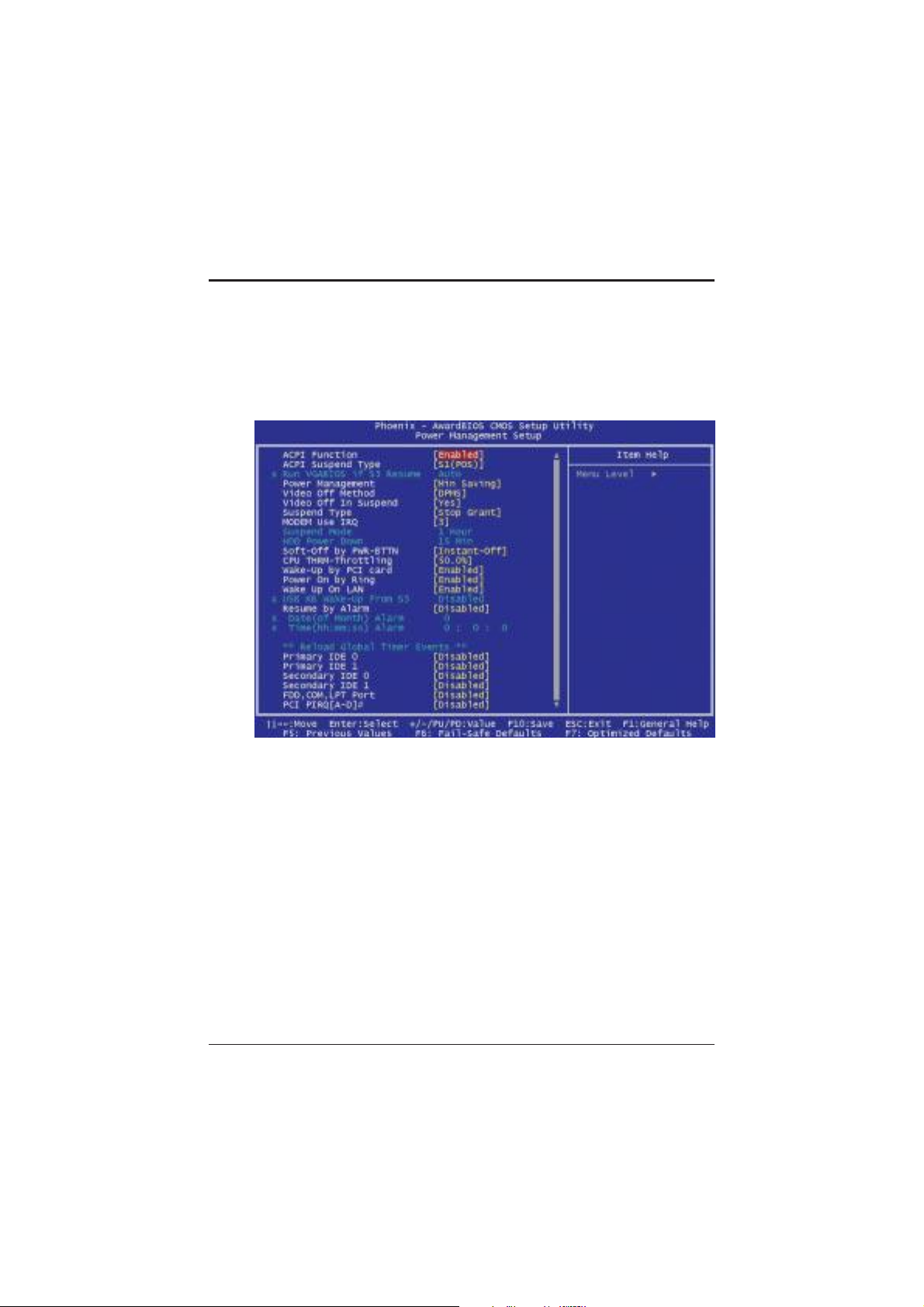
Mainboard Users Manual
4.6. Power Management Setup
Power Management Setup controls the mainboards Green features.
Selecting Power Management Setup on the main program screen
displays this menu:
ACPI Function: When set to Enabled, turns on the ACPI Function. The
default setting is Enabled.
Note: ACPI (Advanced Configuration and Power Interface) is a power
management specification that makes hardware status informa-
tion available to the operating system. ACPI enables a PC to turn
its peripherals on and off for improved power management. It
also allows the PC to be turned on and off by external devices, so
that mouse or keyboard activity wakes up the computer.
48
Power Management setup
Page 55

BIOS Configuration
ACPI Suspend Type: Use this item to define how your system suspends.
If set to S1(POS) (default), the suspend mode is equivalent to a software
power down. If set to S3(STR), the suspend mode is a suspend to RAM
the system shuts down with the exception of a refresh current to the
system memory.
Run VGABIOS if S3 Resume: This item to set run VGABIOS when S3
resume. The default setting is Auto, other options are Yes,or No.
Power Management: This item acts like a master switch for the powersaving modes and hard disk timeouts. If this item is set to Max Saving,
power-saving modes occur after a short timeout. If this item is set to Min
Saving, power-saving modes occur after a longer time-out. If the item is
set to User Define, you can insert your own timeouts for the power-saving
modes. There are four options:
r User Define: allows you to customize all power saving timer features
r Max Saving: recommended setting for general use
r Min Saving: sets power saving at minimum values
Video Off Method: This setting controls the video off method in power
saving mode. The DPMS (default) option allows the BIOS to control the
video card if it has the DPMS (Display Power Management System)
feature. Other options are V/H SYNC+Blank and Blank Screen. The
V/H SYNC+Blank which disables V/H SYNC signals and blanks the
screen. The Blank Screen option is used when you do not have a
Green monitor.
Video Off In Suspend: This item determines the manner in which the
monitor is blanked. The default setting is Yes.
Suspend Type: If this item is set to the default Stop Grant, the CPU will
go into the Idle Mode during suspend mode.
Power Management setup
49
Page 56

Mainboard Users Manual
MODEM Use IRQ: If you want an incoming call on a modem to automatically resume the system from a power-saving mode, use this item to
specify the interrupt request line (IRQ) that is used by the modem. You
might have to connect the fax/modem to a mainboard Wake On Modem
connector for this feature to work. Options are: 3 (default), 4, 5, 7,
9, 10, 11, or NA.
Suspend Mode: Enables you to set the idle time before the system goes
into suspend mode. Options are from Disabled, 1 Min, 2 Min, 4 Min, 8
Min, 12 Min, 20 Min, 30 Min, 40 Min, or 1 Hour. The default is Disabled.
HDD Power Down: The IDE hard drive will spin down if it is not accessed
within a specified length of time. Options are from 1 Min to 15 Min
and Disable. The default is Disabled.
Soft-Off by PWR-BTTN: When set to Instant-Off (default), pressing
the power button will turn off the system power. When set to Delay 4
Sec. you have to press the power button and hold it for more than 4
seconds to turn off the system power. Otherwise, the system just goes
into suspend mode. The options are Instant-Off or Delay 4 Sec.
CPU THRM-Throttling: This item sets the percentage of time that the
CPU is idled if CPU throttling is initiated by excess heat. The options are:
r 50.0% (default)
r 37.5%
r 25.0%
r 12.5%
r 87.5%
r 75.0%
r 62.5%
Wake-Up by PCI card: Enables PCI card activity wake the system from
suspend mode. The default is Enabled.
50
Power Management setup
Page 57

BIOS Configuration
Power On by Ring: When set to Enabled, any activity on the Modem
port will wake up the system from a power saving mode. The options are
Enabled(default) and Disabled .
Wake Up on LAN: Enables LAN activity wake the system from suspend
mode. The default is Enabled.
USB KB Wake-Up From S3: If the ACPI Suspend Type is set to S3(STR) or
S1&S3, you can enable this field to allow USB keyboard activity to wake the
system from suspend mode. The default is Disabled.
Resume by Alarm: When set to Enabled, you may set the date (day of
the month), hour, minute and second to turn on your system. When set to
set 0 (zero) for the day of the month, the alarm will power on your
system every day at the specified time. The default is Disabled.
============ Reload Global Timer Events =============
These fields determine which events waken the system from power saving
mode.
Primary/Secondary IDE 0/1: When enabled, the system power will
resume the system from a power saving mode if there is any activity on
primary or secondary IDE channels 0 or 1. The default is Disabled.
FDD, COM, LPT Port: When this item is enabled, the system will restart the
power-saving timeout counters when any activity is detected on the floppy
disk drive, serial ports, or the parallel port. The default is Disabled.
PCI PIRQ[A-D]#: When set to Enabled, any activity from one of the
listed devices wakes up the system. The default is Disabled.
Press the <ESC> key to go back to the main program screen after you
have made your selections in the Power Management Setup screen.
Integrated Peripherals
51
Page 58
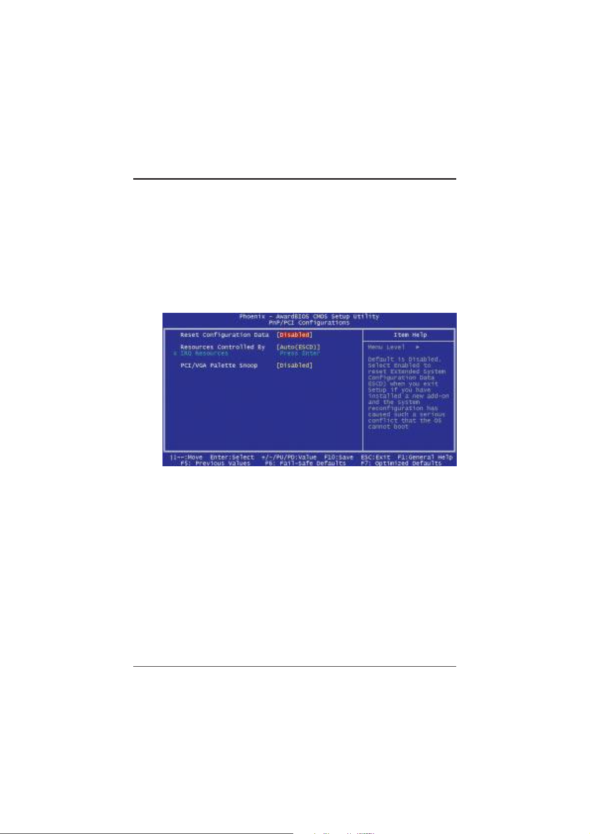
Mainboard Users Manual
4.7. PnP/PCI Configurations
Both the ISA and PCI buses on the Mainboard use system IRQs (Interrupt ReQuests) and DMAs (Direct Memory Access). You must set up
the IRQ and DMA assignments correctly through the PnP/PCI Configuration Setup utility; otherwise, the mainboard will not work properly.
Selecting PnP/PCI Configurations on the main program screen dis-
plays this menu:
Reset Configuration Data: The system BIOS supports the Plug and Play
feature so the resources assigned to each peripheral have to be recorded to
prevent them from conflicting. The location to store the assigned resources
is called ESCD (Extended System Configuration Data) which is located in the
system flash EEPROM. If this option is set to Disabled, the ESCD will
update automatically when the new configuration varies from the last one. If
set to Enable, the ESCD will be cleared and updated and then this option
will automatically be set to Disabled.
Resources Controlled By: The setting is Manual which allows you to
control IRQs and DMAs individually. The other option is Auto(ESCD)
(default) which will detect the system resources and automatically assign
the relative IRQs and DMAs for each peripheral.
IRQ Resources: When resources are controlled manually, assign each
52
PnP/PCI Configurations
Page 59

BIOS Configuration
system interrupt a type, depending on the type of device using the
interrupt.
IRQ3/4/5/7/9/10/11/12/14/15 assigned to: This item allows you to
determine the IRQ assigned to the ISA bus and is not available to any
PCI slot. Legacy ISA for devices is compliant with the original PC AT
bus specification; PCI/ISA PnP (default) for devices is compli-ant with
the Plug-and-Play standard whether designed for PCI or ISA bus
architecture.
PCI/VGA Palette Snoop: This item is designed to overcome some
problems that can be caused by some non-standard VGA cards. This
board includes a built in VGA system that does not require palette
snooping so you must leave this item disabled. The default setting is
Disabled.
After you have made your selections in the PnP/PCI Configurations, press
the <ESC> key to go back to the main program screen.
PnP/PCI Configurations
53
Page 60
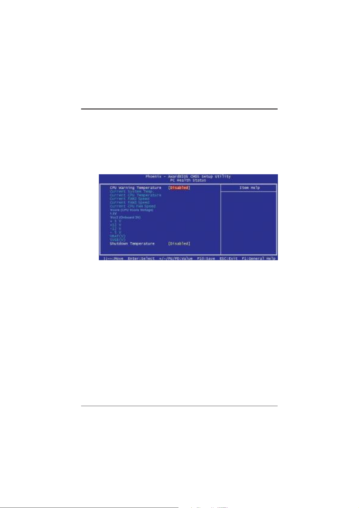
Mainboard Users Manual
4.8. PC Health Status
On mainboards that support hardware monitoring, this item lets you
monitor the parameters for critical voltages, critical temperatures, and fan
speeds. Selecting PC Health Status on the main program screen
displays this menu:
CPU Warning Temperature: This feature enables you to set the warning
temperature for CPU overheating. When the CPU temperature exceeds the
set temperature, the PC speaker will beep. The beep sound will not turn off
unless you power down the computer and allow your CPU to cool down.
System Component Characteristics: These fields provide you with
information about the systems current operating status. You cannot make
changes to these fields. The following information is displayed:
u Current System Temp.
u Current CPU Temperature
u Current FAN2 speed
u Current FAN3 speed
u Current CPU FAN Speed
u Vcore (CPU Vcore Voltage)
54
PC Health Status
Page 61

BIOS Configuration
u 1.5V
u Vcc3 (Onboard 3.3V)
u 5V (Power Supply Voltage)
u 12V (Power Supply Voltage)
u -12V (Power Supply Voltage)
u -5V (Power Supply Voltage)
u VBAT (V) (CMOS Battery Voltage)
u 5VSB (V) (Standby 5V)
Shutdown Temperature: Enables you to set the maximum temperature the
system can reach before powering down. The default settings is 60°C/
140°.
After you have made your selections in the PC Health Status Setup, press
the <ESC> key to go back to the main program screen.
4.9. Frequency/Voltage Control
PC Health Status
55
Page 62
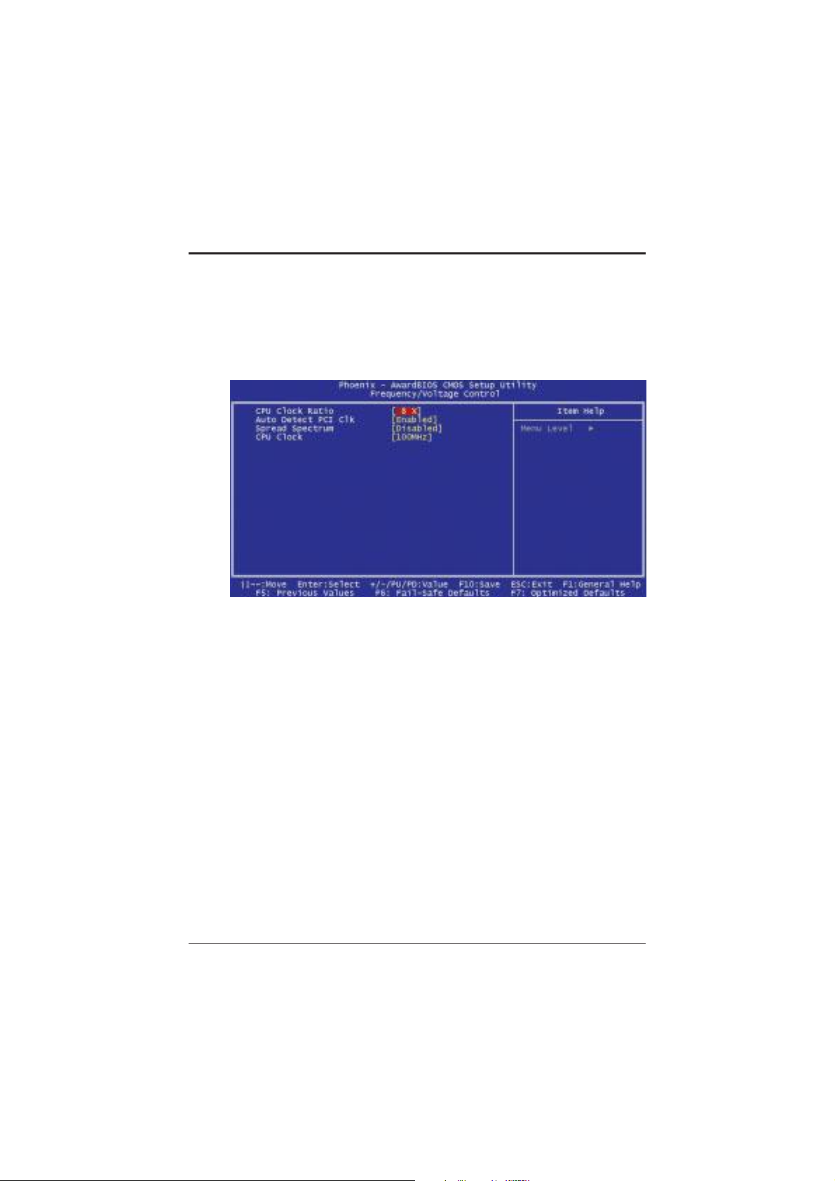
Mainboard Users Manual
This item enables you to set the clock speed and system bus for your
system. The clock speed and system bus are determined by the kind of
processor you have installed in your system.
CPU Clock Ratio: This item allows the user to adjust CPU Ratio. The
values for this field range from 8 to 50.
Auto Detect PCI Clk: When set to Enabled (default), the system will
automatically turn off the PCI clock when not in use to reduce electromagnetic interference.
Spread Spectrum: If you enable spread spectrum, it can significantly
reduce the EMI (Electro-Magnetic Interference) generated by the system.
The default setting is Disabled.
CPU Clock: This item appears if you have set the CPU Internal Core
Speed to Manual. Use the CPU/PCI Clock to set the system bus frequency
for the installed processor. The values for this field range from 100MHz to
165 MHz.
After you have made your selections in the Frequency/Voltage Control
Setup, press the <ESC> key to go back to the main program screen.
56
Frequency/Voltage Control
Page 63

BIOS Configuration
4.10. Load Optimized Defaults Option
This option opens a dialog box that lets you install optimized defaults for
all appropriate items in the whole Setup Utility.
Press the <Y> key and then <Enter> to install the defaults.
Press the <N> key and then <Enter> to not install the defaults.
The optimized defaults place demands on the system that may be greater
than the performance level of the components, such as the CPU and the
memory. You can cause fatal errors or instability if you install the optimized
defaults when your hardware does not support them. If you only want to install setup defaults for a specific option, select and display that option, and
then press the <F7> key.
Load Optimized Defaults Option
57
Page 64
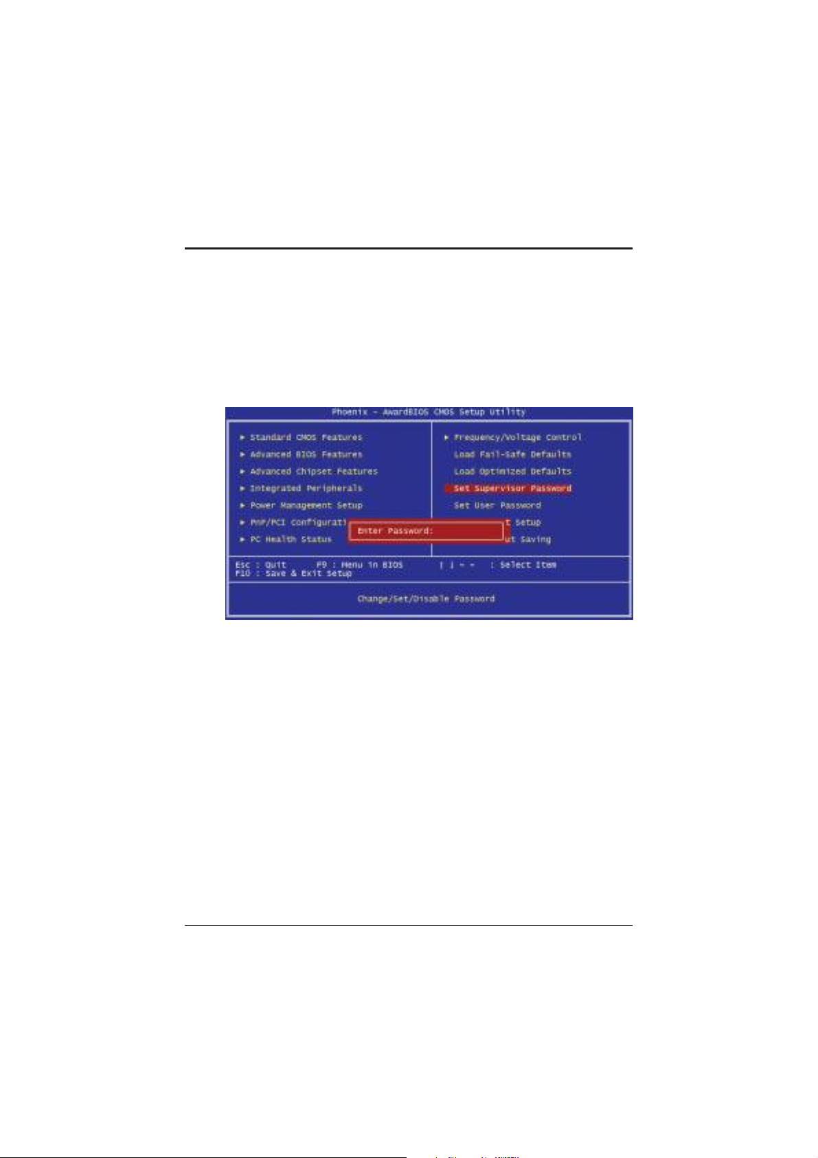
Mainboard Users Manual
4.11. Set Supervisor/User Password
The Set Supervisor/User Password utilities set the passwords.
The mainboard is shipped with the password disabled. If you want to
change the password, you must first enter the current password, then at
the prompt enter your new password. The password is case sensitive. You
can use up to eight alphanumeric characters.
Press <Enter> after entering the password. At the next prompt, confirm
the new password by retyping it and pressing <Enter> again.
To disable the password, press <Enter> instead of entering a new
password when the Enter Password dialog box appears. A message
appears confirming that the password has been disabled.
If you have set supervisor and user passwords, only the supervisor
password allows you to enter the BIOS Setup Program.
Note: If you forget your password, the only way to solve this problem
is to discharge the CMOS memory by turning power off and
placing a shunt on jumper JP12 to short pin 1 and pin 2 for five
seconds, then putting the shunt back to pin 2 and pin 3 of JP12.
58
Set Supervisor/User Password
Page 65

BIOS Configuration
4.12. Save & Exit Setup
Selecting this option and pressing <Enter> will save the new setting
information in the CMOS memory and continue with the booting process.
4.13. Exit Without Saving
Selecting this option and pressing <Enter> will exit the Setup Utility
without recording any new values or changing old ones.
This concludes Chapter 4. Chapter 5 describes the drivers and utility
programs that are packaged with the mainboard.
59Save & Exit Setup
Page 66

Mainboard Users Manual
5. Driver and Utility
5.1. Flash Utility
The BIOS of the P8F151 mainboard can be upgraded by using a Flash
utility. A new version of the BIOS can be downloaded from the factorys
BBS and Web site. The system BIOS is stored in a 2 M-bit Flash EEPROM
that can be erased and reprogrammed by the Flash utility.
There are two files in the D:\DRIVER\FLASH directory:
r FLASH.EXE Flash utility for AWARD BIOS upgrade
r README.TXT Text file of instructions
The Flash utility will not work with any memory manager software
running in the system. In order to make sure no memory manager software
is running, boot your system from a bootable floppy diskette which does
not contain CONFIG.SYS and AUTOEXEC.BAT files. If you are using
MS-DOS 6.x, you can press the <F5> function key when the Starting
MS-DOS. message appears on the screen to by pass the CONFIG.SYS
and AUTOEXEC.BAT.
60
Driver and Utility
Page 67
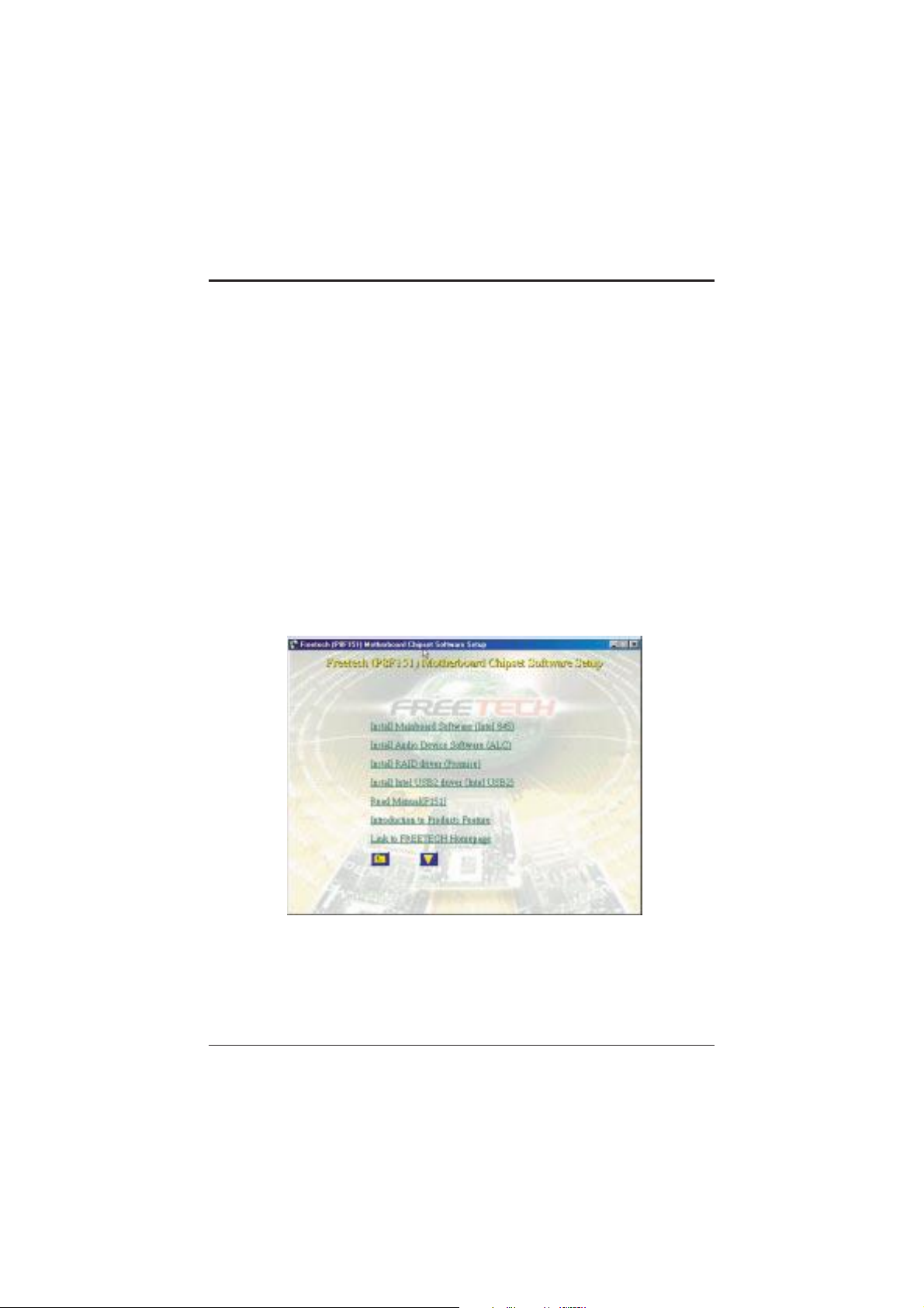
Driver and Utility
5.2. CD Driver Overview
The mainboard has drivers and utilities designed for the Intel 845 chipset.
You can install AGP, IRQ, ACPI and IDE drivers together from the
manufacturers support CD. The support CD has an easy to use menu that
enables you to automatically install the drivers and software that you want.
To start your mainboard CD disc, insert into your CD-ROM drive and the
CD AutoRun screen should appear. If the AutoRun screen does not
appear, duble click or run D:\ Autorun.exe (assuming that your CD-ROM
drive is drive D:)
The P8F151 CD include
1. Install Mainboard Software (Intel 845)
2. Install Audio Device Software (ALC)
3. Install RAID driver (Promise)
4. Install Intel USB2 driver (Intel USB2)
Click the links to install the listed software, read the online manual, read a
list of the mainboards features, or browse to the Freetech homepage.
You can also browse the CD and install the software manually from
Windows Explorer We recommend that you install all of the supplied
software and drivers items for maximum performance.
CD Driver Overview
61
Page 68

Mainboard Users Manual
5.2.1. Intel chipset 845 INF driver
This folder has chipset 845 INF drivers for Windows Millennium/2000/98/
95/XP.
The Installation Steps:
1. Insert the manufacturer CD-ROM into your CD-ROM drive.
2. Click Driver Install.
3. Select the folder Driver\Intel\Inf driver for WIN2000/9X/ME or
XP to start the installation:
4. Follow the instructions on the screen to complete the installation.
After setup is completed, you need to restart the computer.
5.2.2 . Intel chipset 845 Busmater IDE driver
This folder has chipset 845 Busmater IDE drivers for Windows Millennium/2000/98/95/NT.
The Installation Steps:
1. Insert the manufacturers CD-ROM into your PCs CD-ROM
drive.
2. Click Driver Install.
3. Select the folder Driver\Intel\IAA\Disk1 driver for WIN2000/
9X/NT40/ME to start the installation:
4. Follow the instructions on the screen to complete the installation.
After setup is completed, you need to restart the computer.
62 CD Driver Overview
Page 69

Driver and Utility
5.2.3. ALC201 Audio Driver
Software and drivers are provided for the 82801DB codec sound system
that is integrated on this mainboard. The 82801DB codec allows the
system to generate optimal sound effects. Drivers are provided for
Windows NT/2000/98SE/95/ME/XP.
The manual Installation Steps:
1. Insert the manufacturers CD-ROM into your PCs CD-ROM drive.
2. Click Driver Install.
3. Select the folder Driver\Sound\ALC driver for WIN98SE,
WIN2000/WIN95/WINNT/WINME/WINXP to start the installation:
4. Follow the instructions on the screen to complete the installation.
After setup is completed, you need to restart the computer.
63CD Driver Overview
Page 70

Driver and Utility
5.3. Online Services
Flexus Computer Technology, under the Freetech brand name, has consistently won recognition for excellence in the design and manufacturing of
high quality mainboards!
Our products are globally recognized among the leading cost-performance
mainboards in the industry today and we are a certified ISO-9002 manufacturer!
Our customers are our partners! Flexus practices partnership service not
customer service! Our attention to partnership service is aggressive and
proactive, by using our global partnership service system. We create value
for our partners in the high-end market and we are always ready to see to our
partners requirements, because at Flexus, we believe our partners success
is our success!
If you need technical support, information on products, or updated
versions of the BIOS, drivers and utilities access the Internet and point
your browser to:
www.freetech.com
Online Services
 Loading...