

Page 1

Freescale Semiconductor, Inc.
User’s Guide
Document Number: USBKW40ZUG
Rev. 0, 10/2015
Freescale USB Development Board
USB-KW40Z User's Guide
1 About this guide
This manual describes the Freescale USB-KW40Z
development platform. The USB-KW40Z board is a small,
cost-effective evaluation and development board for
application prototypes and demonstration of the
MKW40Z160 SoC family of devices. This evaluation board
offers an easy-to-use mass-storage device mode flash
programmer, a virtual serial port, classic programming, and
run-control capabilities.
The MKW40Z160 SoC is an ultra low-power, highly
integrated single-chip device that enables Bluetooth Low
Energy (BLE) and/or IEEE® Std. 802.15.4/RF connectivity
for portable, extremely low-power embedded systems. The
MKW40Z160 SoC family integrates a radio transceiver
operating in the 2.36 GHz to 2.48 GHz range supporting a
range of FSK/GFSK and O-QPSK modulations, and ARM
Cortex®- M0+ MCU, 160 KB flash memory and 20 KB
SRAM, BLE Link Layer hardware, 802.15.4 packet
processor hardware, and peripherals optimized to meet the
requirements of the target applications.
Contents
1. About this guide . . . . . . . . . . . . . . . . . . . . . . . . . . . . . 1
1.1.Audience . . . . . . . . . . . . . . . . . . . . . . . . . . . . . . . . 1
2. Safety information . . . . . . . . . . . . . . . . . . . . . . . . . . . 2
2.1.FCC guidelines . . . . . . . . . . . . . . . . . . . . . . . . . . . 2
2.2.Regulatory approval for Canada (IC RSS 210) . . . 3
2.3.Electrostatic discharge considerations . . . . . . . . . . 3
2.4.Disposal instructions . . . . . . . . . . . . . . . . . . . . . . . 3
3. USB-KW40Z overview and description . . . . . . . . . . 4
3.1.Introduction . . . . . . . . . . . . . . . . . . . . . . . . . . . . . . 4
3.2.Board features . . . . . . . . . . . . . . . . . . . . . . . . . . . . 4
3.3.Serial and debug adapter . . . . . . . . . . . . . . . . . . . . 6
4. USB-KW40Z development board . . . . . . . . . . . . . . . 7
4.1.USB-KW40Z board overview . . . . . . . . . . . . . . . . 7
4.2.Functional description . . . . . . . . . . . . . . . . . . . . . . 9
4.3.Schematic, board layout, and bill of material . . . 16
5. PCB manufacturing specifications . . . . . . . . . . . . . . 21
5.1.Single PCB construction . . . . . . . . . . . . . . . . . . . 21
5.2.Panelization . . . . . . . . . . . . . . . . . . . . . . . . . . . . . 22
5.3.Materials . . . . . . . . . . . . . . . . . . . . . . . . . . . . . . . 22
®
5.4.Solder mask . . . . . . . . . . . . . . . . . . . . . . . . . . . . . 23
5.5.Silk screen . . . . . . . . . . . . . . . . . . . . . . . . . . . . . . 23
5.6.Electrical PCB testing . . . . . . . . . . . . . . . . . . . . . 23
5.7.Packaging . . . . . . . . . . . . . . . . . . . . . . . . . . . . . . 23
5.8.Hole specification/tool table . . . . . . . . . . . . . . . . 23
5.9.File description . . . . . . . . . . . . . . . . . . . . . . . . . . 23
6. Revision history . . . . . . . . . . . . . . . . . . . . . . . . . . . . 24
1.1 Audience
This manual is intended for system designers.
© 2015 Freescale Semiconductor, Inc. All rights reserved.
Page 2

Safety information
2 Safety information
2.1 FCC guidelines
This equipment is for use by developers for evaluation purposes only and must not be incorporated into
any other device or system. This device may not be sold to the general public. Integrators will be
responsible for reevaluating the end product (including the transmitter) and obtaining a separate FCC
authorization.
FCC approval of this device only covers the original configuration of this device as supplied. Any
modifications to this product, including changes shown in this manual, may violate the rules of the Federal
Communications Commission and Industry Canada and make operation of the product unlawful.
2.1.1 Labeling
FCC labels are physically located on the back of the board.
2.1.2 Operating conditions
This device complies with part 15 of the FCC rules. Operation is subject to the following two conditions:
• This device may not cause harmful interference.
• This device must accept any interference received, including interference that may cause undesired
operation.
2.1.3 Exposure limits
This equipment complies with FCC radiation exposure limits set forth for an uncontrolled environment.
The antenna(s) used for this equipment must be installed to provide a separation distance of at least 8
inches (20 cm) from all persons.
2.1.4 Antenna restrictions
An intentional radiator is designed to ensure that no antenna other than that furnished by the responsible
party is used with the device. The use of a permanently attached antenna or of an antenna that uses a unique
coupling to the intentional radiator is considered sufficient to comply with the provisions of this Section.
The manufacturer may design the unit so that a broken antenna can be replaced by the user, but the use of
a standard antenna jack or electrical connector is prohibited. This requirement does not apply to carrier
current devices or to devices operated under the provisions of Sections 15.211, 15.213, 15.217, 15.219, or
15.221 of the IEEE Std. 802.15.4. This requirement does not apply to intentional radiators that must be
professionally installed, such as perimeter protection systems and some field disturbance sensors, or to
other intentional radiators which, in accordance with Section 15.31(d), must be measured at the installation
site. However, the installer is responsible for ensuring that the proper antenna is employed so that the limits
in this Part are not exceeded.
Freescale USB Development Board USB-KW40Z User’s Guide, Rev. 0, 10/2015
2 Freescale Semiconductor, Inc.
Page 3

Safety information
2.2 Regulatory approval for Canada (IC RSS 210)
This equipment complies with Industry Canada licence-exempt RSS standard(s). Operation is subject to
the following two conditions:
1. This board may not cause interference, and
2. This board must accept any interference, including interference that may cause undesired operation
of the device.
2.2.1 26 PART 5 – Appendix
Le présent appareil est conforme aux CNR d'Industrie Canada applicables aux appareils radio exempts de
licence. L'exploitation est autorisée aux deux conditions suivantes:
1. l'appareil ne doit pas produire de brouillage, et
2. l'utilisateur de l'appareil doit accepter tout brouillage radioélectrique subi, même si le brouillage
est susceptible d'en compromettre le fonctionnement.
2.3 Electrostatic discharge considerations
Although damage from electrostatic discharge (ESD) is much less common on these devices than on early
CMOS circuits, normal handling precautions should be used to avoid exposure to static discharge.
Qualification tests are performed to ensure that these devices can withstand exposure to reasonable levels
of static without suffering any permanent damage.
All ESD testing is in conformity with the JESD22 Stress Test Qualification for Commercial Grade
Integrated Circuits. During the device qualification ESD stresses were performed for the human body
model (HBM), the machine model (MM) and the charge device model (CDM).
All latch-up test testing is in conformity with the JESD78 IC Latch-Up Test.
When operating or handling the development boards or components, Freescale strongly recommends
using at least the grounding wrist straps plus any or all of the following ESD dissipation methods:
• Flexible fabric, solid fixed size, or disposable ESD wrist straps
• Static control workstations, static control monitors, and table or floor static control systems
• Static control packaging and transportation materials and environmental systems
2.4 Disposal instructions
This product may be subject to special disposal requirements. For product disposal instructions, refer to
freescale.com/productdisposal.
Freescale USB Development Board USB-KW40Z User’s Guide, Rev. 0, 10/2015
Freescale Semiconductor, Inc 3
Page 4
USB-KW40Z overview and description
3 USB-KW40Z overview and description
3.1 Introduction
The USB-KW40Z development platform is an evaluation environment based on the Freescale
MKW40Z160 SoC device. The MKW40Z160 SoC integrates a radio transceiver operating in the 2.36 GHz
to 2.48 GHz range, supporting a range of FSK/GFSK and O-QPSK modulations, an ARM Cortex-M0+
MCU into a single package.
Freescale supplements the MKW40Z160 SOC with tools and software that include hardware evaluation
and development boards, software development IDE, applications, drivers, custom PHY usable with IEEE
Std. 802.15.4 compatible MAC, BLE Link Layer, and enables the Bluetooth Low Energy protocol to be
used in the MBAN frequency range for proprietary applications.
3.2 Board features
3.2.1 USB-KW40Z board
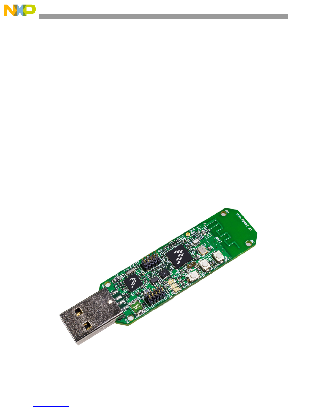
The USB-KW40Z development board contains the MKW40Z160 device it is one of the simplest reference
design utilizing the on chip USB block for power and communication. The USB-KW40Z is a small form
factor self-contained board for evaluation of wireless application and can be used as a packet sniffer. The
USB type-A connection is used with USB enabled hardware such as a computer.
Figure 1 shows the USB-KW40Z development platform.
Freescale USB Development Board USB-KW40Z User’s Guide, Rev. 0, 10/2015
4 Freescale Semiconductor, Inc.
Figure 1. USB-KW40Z development board
Page 5

USB-KW40Z overview and description
The USB-KW40Z development board includes the following features:
• Based on the Freescale ultra low-power MKW40Z160 SoC BLE device
• Fully compliant IEEE Std. 802.15.4, 2006, transceiver supporting 250 kbit/s O-QPSK data in
5.0 MHz channels and full spread-spectrum encode and decode
• Fully compliant Bluetooth v4.1 Low Energy (BLE)
• Full IEEE 802.15.4 compliant wireless node with KSDK enable software
• Reference design area with small footprint, low-cost RF node
— Differential input/output port used with external balun for single port operation
— Low external component count
— Programmable output power from –20 dBm to +5 dBm at the MMCX connector, no harmonic
trap using bypass mode of operation
— Receiver sensitivity: –102 dBm, typical (@1% PER for 20 byte payload packet), for 802.15.4
at the MMCX connector
— Receiver sensitivity: -91 dBm for BLE applications at the MMCX connector
• Integrated PCB inverted meander type antenna and MMCX (Micro-Miniature Coaxial) RF port
• Bypass operation mode
• 32 MHz reference oscillator
• 32 kHz reference oscillator
• 2.4 GHz frequency operation (ISM and MBAN)
• Reset switch drive to MKW40Z160.
• Reset switch drive to debug interface (OpenSDA)
• Cortex 10-pin (0.05 inch) SWD debug port for target MCU
• Cortex 10-pin (0.05 inch) JTAG port for OpenSDA updates
• Integrated open-standard serial and debug interface (OpenSDA)
• 2 Blue LED indicators primary drive thought MKW40Z160 MCU, also connected to MK22FN512
• 1 Push button switch drive to MKW40Z160 MCU, also connected to MK22FN512
Freescale USB Development Board USB-KW40Z User’s Guide, Rev. 0, 10/2015
Freescale Semiconductor, Inc 5
Page 6
USB-KW40Z overview and description
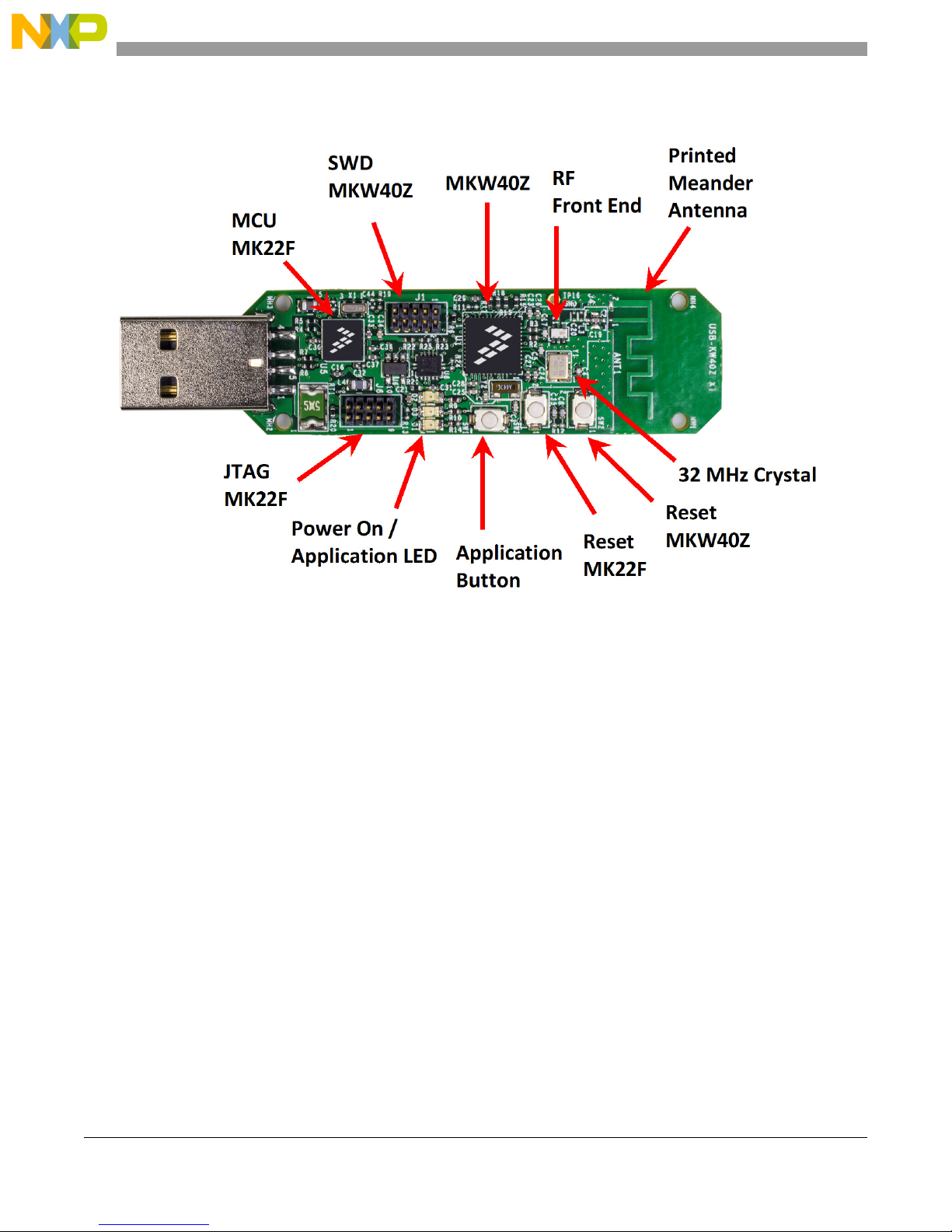
Figure 2 shows the main board features and I/O headers for the Freescale USB-KW40Z board.
Figure 2. USB-KW40Z component placement
3.3 Serial and debug adapter
The USB-KW40Z development board can be enabled with OpenSDA v2.1, a serial and debug adapter
circuit that includes an open-source hardware design, an open-source bootloader, and debug interface
software. It bridges serial and debug communications between a USB host and an embedded target
processor. The hardware circuit is based on a Freescale Kinetis K22F family microcontroller (MCU).
OpenSDAv2.1 enables the CMSIS-DAP bootloader, an open-source mass storage device (MSD)
bootloader, and the CMSIS-DAP Interface firmware (also known as the mbed interface), that provides a
MSD flash programming interface, a virtual serial port interface, and a CMSIS-DAP debug protocol
interface. For more information on the OpenSDAv2.1 software, see mbed.org and
https://github.com/mbedmicro/CMSIS-DAP.
NOTE
Driver considerations, you must install a windows driver that can be
downloaded from the following link:
https://developer.mbed.org/handbook/Windows-serial-configuration
USB-KW40Z comes pre-programed with a sniffer application. In order to enable this board with
OpenSDA feature and as a development board, refer to the following:
freescale.com/USB-KW40Z/startnow
Freescale USB Development Board USB-KW40Z User’s Guide, Rev. 0, 10/2015
6 Freescale Semiconductor, Inc.
Page 7
USB-KW40Z development board
4 USB-KW40Z development board
4.1 USB-KW40Z board overview
The USB-KW40Z board is an evaluation board based on the Freescale MKW40Z160 SoC. The
USB-KW40Z provides a platform to evaluate the MKW40Z160 SoC device and to develop software and
applications. The core device is accompanied by a the 32 MHz reference oscillator crystal, RF circuitry
including antenna, and supporting circuitry.
The USB-KW40Z board is intended as the core PCB for MKW40Z160 device evaluation and application
development, and can be used as a simple standalone valuation solution or as packet sniffer.
4.1.1 PCB features
The USB-KW40Z board provides the following features:
• USB small form factor
• 4-Layer metal, 0.062 inch thick FR4 board
• LGA footprint and power supply bypass mode
• Printed Meander Antenna and footprint for installing a (user supplied) MMCX connector
• 32 MHz reference oscillator crystal
• 32 kHz crystal provided for optional timing oscillator
• Secondary (MK22FN512) device to use as voltage regulator and MCU processor for BLE sniffer.
4.1.2 Form factor
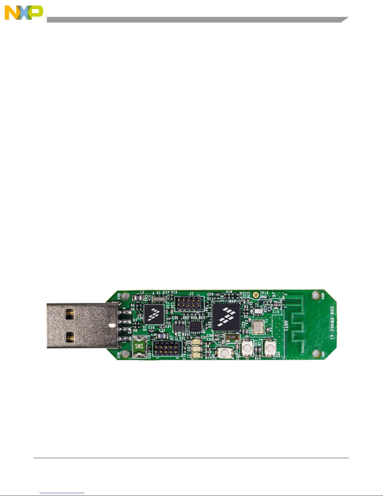
Figure 3 shows the USB-KW40Z development board layout and footprint.
Figure 3. USB-KW40Z top side (component side) footprint
Freescale USB Development Board USB-KW40Z User’s Guide, Rev. 0, 10/2015
Freescale Semiconductor, Inc 7
Page 8
USB-KW40Z development board
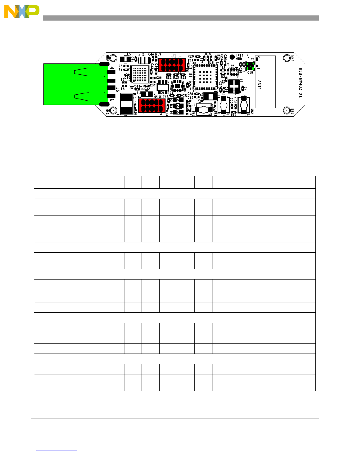
Figure 4 shows a footprint of the USB-KW40Z with the location of the headers.
Figure 4. USB-KW40Z I/O headers location
4.1.3 Board level specifications
Table 1. USB-KW40Z specifications
Parameter Min Typ Max Units Notes/Conditions
General
Size (PCB: X, Y) — — 18.5 x 61.4
0.73 x 2.42mminches
Layer build (PCB) — 1.57
0.062
Dielectric material (PCB) — — — — FR4
Power
Current consumption — — — mA Varies with operational mode, Refer to
Tem per atur e
Operating temperature (see note) -40 +25 +70 °C Operating temperature is limited to +70 °C
Storage temperature -30 +25 +70 °C
RF
802.15.4 Frequency range 2405 — 2480 MHz All 16 channels in the 2450 MHz band
BLE Frequency range 2400 — 2483 MHz All 40 channels in the 2450 MHz band
ISM and MBAN Frequency range 2360 — 2483 MHz
RF Receiver
—mm
inches
4-Layer
datasheet.
due to switches. Basic circuit is good for a
maximum temperature of +85 °C.
Saturation (maximum input level) — +0 — dBm Refer to datasheet
Sensitivity for 1% packet error rate
(PER) (+25 °C) 802.15.4
Freescale USB Development Board USB-KW40Z User’s Guide, Rev. 0, 10/2015
8 Freescale Semiconductor, Inc.
— -102 — dBm Refer to datasheet
Page 9

USB-KW40Z development board
Table 1. USB-KW40Z specifications (continued)
Parameter Min Typ Max Units Notes/Conditions
Sensitivity for 1% packet error rate
(PER) (+25 °C) BLE
RF Transmitter
RF Power Output -20 — +5 dBm Programmable in steps.
2nd harmonic — ≤50 ≤40 dBm —
3rd harmonic — ≤50 ≤40 dBm —
Regulatory Approval
FCC — — — — Product is approved according to the FCC
CE (ETSI) — — — — Product is approved according to the EN
CE (EMC) — — — — Product is approved according to the EN
Safety
UL — — — — Product is approved according to the IEC
Environment
— -94 — dB Refer to datasheet
At the MMCX connector with no trap.
part 15 standard
300 328 V1.7.1 (2006-10) standard
301 489-1 V1.6.1 (2005-09) and EN 301
489-17 V1.2.1 (2002-08) standards
60950-1 and EN 60950-1, First Edition
standards
1
RoHS — — — — Product complies with the EU Directive
2002/95/EC of 27 January 2003
WEEE — — — — Product complies with the EU Directive
2002/95/EC of 27 January 2003
1]
Trap will add 1 to 2 dB of loss.
4.2 Functional description
The USB-KW40Z is built around the Freescale MKW40Z160 SoC in a 48-pin LGA package. The
USB-KW40Z features a IEEE Std. 802.15.4 and BLE 2.4 GHz radio frequency transceiver and a Kinetis
family ultra low-power, mixed-signal ARM Cortex-M0+ microcontroller in a single package. This board
is intended as a simple evaluation platform and as a building block for application development. The
four-layer board provides the MKW40Z160 with its required RF circuitry and a 32 MHz reference
oscillator crystal. The layout for this base level functionality can be used as a reference layout for your
target board. Figure 5 shows a simple block diagram.
Freescale USB Development Board USB-KW40Z User’s Guide, Rev. 0, 10/2015
Freescale Semiconductor, Inc 9
Page 10

USB-KW40Z development board
Figure 5. USB-KW40Z block diagram
4.2.1 RF performance and considerations
The USB-KW40Z board’s integrated transceiver includes a 1 mW nominal output power PA with internal
voltage controlled oscillator (VCO), integrated transmit/receive switch, on-board power supply regulation,
and full spread-spectrum encoding and decoding. Key specifications for the MKW40Z160 SoC are:
• Nominal output power is set to 0 dBm
• Programmable output power from -20 dBm to +5 dBm at the MMCX, no harmonic trap
• Typical sensitivity is -102 dBm (@1% PER for 25 °C) at the MMCX (802.15.4)
• Typical sensitivity is -91 dBm (@1% PER for 25 °C) at the MMCX (BLE)
• Frequency range is 2360 to 2480 MHz
• Differential bidirectional RF I/O port with integrated transmit/receive switch
• Meander printed metal antenna for a small footprint, low cost design
• Uses a minimum number of RF marching components and external 50:100 balun
An external 50 (bal): 100 (unbal) balun connects a single-ended 50 ohm port to the differential RF port of
the MKW40Z160 SoC’s transceiver. The layout has provision for out-of-band signal suppression
(components L3 and C20) if required. Figure 6 shows the typical topology for the RF circuitry. The RF
connector J4 has been included in the design for measurement purposes and is used as a DNP.
Freescale USB Development Board USB-KW40Z User’s Guide, Rev. 0, 10/2015
10 Freescale Semiconductor, Inc.
Page 11

USB-KW40Z development board
Figure 6. USB-KW40Z RF circuitry
4.2.2 Clocks
The USB-KW40Z provides two clock sources to the MKW40Z160:
• 32 MHz Reference Oscillator - Figure 7 shows the external 32 MHz external crystal Y1. This
mounted crystal must meet the specifications outlined in the AN3251 application note. The IEEE
Std. 802.15.4 requires that the frequency be accurate to less than ±40 ppm.
— Capacitors C4 and C5 provide the bulk of the crystal load capacitance. At 25 °C, it is desired
to have the frequency accurate to ±10 ppm or less to allow for temperature variation.
• Optional 32.768 kHz Crystal Oscillator: Provision is also made for a secondary 32.768 kHz crystal
Y2 (see Figure 8). This oscillator can be used for a low power accurate time base.
— The module comes provided with this Y2 crystal and its load capacitors C6 and C7.
— Load capacitors C6 and C7 provide the entire crystal load capacitance; there is no onboard trim
capacitance.
Figure 7. USB-KW40Z board’s 32 MHz reference oscillator circuit
Freescale USB Development Board USB-KW40Z User’s Guide, Rev. 0, 10/2015
Freescale Semiconductor, Inc 11
Page 12

USB-KW40Z development board
Figure 8. USB-KW40Z board’s optional 32.768 kHz oscillator circuit
4.2.3 Power management
There is one way to power on the USB-KW40Z board, a J5 type-A connector to supply 5 V(V_USB)
directly to the secondary MCU, that includes an internal regulator, 3.3 V output to enable theMKW40Z160
device. The USB-KW40Z power management circuit is shown in Figure 9.
Figure 9. USB-KW40Z power management circuit
Additionally, a green LED marked as D1 is available as a power indicator. For current measurements, users
can isolate the MKW40Z160
device, through SH13 cut-trace, this will disable the VCC path (including
LED).
Freescale USB Development Board USB-KW40Z User’s Guide, Rev. 0, 10/2015
12 Freescale Semiconductor, Inc.
Page 13

USB-KW40Z development board
4.2.4 USB-KW40Z peripheral functions
The board includes two different MCUs, one dedicated to RF (MKW40Z160) acquisition and the second
features an OpenSDA debugger and processor for BLE sniffer application (MK22FN512).
4.2.4.1 MKW40Z160 peripheral functions
The USB-KW40Z development board includes two push buttons: one for a general purpose peripheral
function to assist in implementing targeted applications and the other dedicated to MKW40Z160 hardware
reset.
The board also include three LEDs, two for general purposes and the other as a Power-On indicator.
Figure 10 shows the push buttons and LEDs for MKW40Z160.
The application LEDs (D2 and D3) are connected not only with MKW40Z, they also share this connection
with the MK22FN512 MCU. You can isolate LEDs to remove or cut the trace over SH5 and SH6.
Figure 10. USB-KW40Z MKW40Z160 push button & LED
4.2.4.2 MK22FN512/Open SDA Interface
• The USB-KW40Z includes an OpenSDA circuitry based on the MK22FN512, that includes all the
necessary components to enable communication and debugging, it also provides power output to
all MKW40Z160
MCU, and all the necessary connections to interface with MKW40Z160
Freescale USB Development Board USB-KW40Z User’s Guide, Rev. 0, 10/2015
peripherals. Figure 11 shows the OpenSDA circuitry based on the MK22FN512
.
Freescale Semiconductor, Inc 13
Page 14

USB-KW40Z development board
Freescale USB Development Board USB-KW40Z User’s Guide, Rev. 0, 10/2015
14 Freescale Semiconductor, Inc.
Figure 11. USB-KW40Z OpenSDA circuitry
Page 15

USB-KW40Z development board
4.2.4.2.1 OpenSDA interface clock
The USB-KW40Z provides one clock source for the OpenSDA MK22FN512 MCU.
• 8 MHz Reference Oscillator - Figure 12 shows the external 8 MHz external crystal X1. This
mounted crystal must meet MK22FN512 specifications. It also provides C44 and C45 to the bulk
of the crystal load capacitance.
Figure 12. USB-KW40Z MK22FN512 8 MHz clock source
4.2.4.2.2 MK22FN512 peripheral functions
The USB-KW40Z OpenSDA interface circuit also includes one switch button, to assist in MK22FN512
MCU hardware reset. Figure 13 shows the push button for MK22FN512
Figure 13. USB-KW40Z MK22FN512 push button & LED
Freescale USB Development Board USB-KW40Z User’s Guide, Rev. 0, 10/2015
Freescale Semiconductor, Inc 15
Page 16

USB-KW40Z development board
5
5
4
4
3
3
2
2
1
1
D D
C C
B B
A A
POWER ON
IN CIRCUIT
TEST GND
PROBING
SWITCH
MKW40 48-pin MCU
Place caps close to DUT
32MHz XTAL
SWD CONNECTOR KW40
RESET
32kHz XTAL
LEDS
100 Ohm controlled
impedance from DUT
to balun.
50 ohm controlled
impedence line from
Balun to SMA and F_Antenna
RF
CAD NOTE:
Embed pads into
50 Ohm line.
HARMONIC TRAP
K22_SIN
K22_SS
K22_SCK
VDD_RF1, VDD_RF2 and VDD_XTAL
CAD NOTE: XTAL close to KW40
CAD NOTE:
MISO/MOSI POKA-YOKE:
Place both
resistors
with the same orientation
and provide same airgap
between MISO to MOSI resistors
terminals in a square fashion.
XTAL_32M
EXTAL_32M
RST_TGTMCU_B
BAL_C
Z_RF_N
Z_RF_P
RF_50 RF_ANT
RF_N
RF_P
UART0_RTS
UART0_CTS
UART0_TX
UART0_RX
VDCDC_IN
P3V3_KW40
GND
P3V3_KW40
P3V3_KW40
P3V3_KW40
P3V3_KW40
P3V3_KW40 P3V3_KW40
P3V3_KW40
P3V3_KW40
P3V3_KW40
P3V3_K22F
P3V3_K22F
P3V3_KW40
KW40_SWD_DIO
pg(3)
RST_TGTMCU_b pg(3,4)
KW40_SWD_CLK pg(3)
PTB2_KW40
XTAL_32K
EXTAL_32K
PTC0_KW40 PTC1_KW40
EXTAL_32M
XTAL_32M
KW40_SWD_CLK{3}
KW40_SWD_DIO{3}
RST_TGTMCU_b{3,4}
EXTAL_32K
XTAL_32K
PTB0_KW40
PTB1_KW40
PTC0_KW40
PTC1_KW40
I2C1_SDA
I2C1_SCL
PTB2_KW40
SPI_SS
SPI_SIN
SPI_SOUT
SPI_CLK UART_CTS
{3}
UART_RTS
{3}
UART_RXD
{3}
UART_TXD
{3}
BSM_FRAME
BSM_DATA
BSM_SCK
Drawing Title:
Size Document Number Rev
Date: Sheet
of
Page Title:
ICAPClassification: FCP: FIUO: PUBI:
X1
X-USB-KW40Z
C
Wednesday, May 13, 2015
MAIN SCHEMATIC
34
___ ___
X
SCH-xxxxxPDF: SPF-xxxxx
Drawing Title:
Size Document Number Rev
Date: Sheet of
Page Title:
ICAPClassification: FCP: FIUO: PUBI:
X1
X-USB-KW40Z
C
Wednesday, May 13, 2015
MAIN SCHEMATIC
34
___ ___
X
SCH-xxxxxPDF: SPF-xxxxx
Drawing Title:
Size Document Number Rev
Date: Sheet of
Page Title:
ICAPClassification: FCP: FIUO: PUBI:
X1
X-USB-KW40Z
C
Wednesday, May 13, 2015
MAIN SCHEMATIC
34
___ ___
X
SCH-xxxxxPDF: SPF-xxxxx
Y2
32.768KHZ
21
MH2
MH_80mil
1
1
MH4
MH_80mil
1
1
R6
10.0K
SH12
0
C26
0.1UF
TP15
TP8
R5
10.0K
C17
0.6PF
R3
0
C20
1.8pF
DNP
C28
0.1UF
C24
12PF
SW1
TL1015AF160QG
1 2
R14
330
D3
RED
AC
C29
0.1UF
R10
330
SW2
TL1015AF160QG
1 2
MKW40Z160VHT4
U1
PTB3/ADC0_SE2/CMP0_IN4/CLKOUT/TPM1_CH1/RTC_CLKOUT/ERCLK32K19PTB16/EXTAL32K/I2C1_SCL/TPM2_CH021PTB17/XTAL32K/I2C1_SDA/TPM2_CH122PTB18/DAC0_OUT/ADC0_SE4/CMP0_IN2/I2C1_SCL/TPM_CLKIN0/TPM0_CH0/NMI23PTB0/I2C0_SCL/CMP0_OUT/TPM0_CH1/CLKOUT16PTB1/ADC0_SE1/CMP0_IN5/I2C0_SDA/LPTMR0_ALT1/TPM0_CH2/CMT_IRO17PTB2/ADC0_SE3/CMP0_IN3/TPM1_CH0
18
VDCDC_IN
10
DCDC_GND
13
VDD_1P8
14
VDD_1P45
15
VDD_0
20
VSSA
26
VREFH
27
VDDA
28
VDD_XTAL
31
VDD_RF2
32
VDD_RF1
35
VDD_1/VDD
44
GND9
57
GND8
56
GND7
55
GND6
54
GND5
53
GND4
52
GND3
51
GND2
50
GND1
49
PTA0/SWD_DIO/TSI0_CH8/SPI0_PCS1/TPM1_CH01PTA1/SWD_CLK/T SI0_CH9/TPM1_CH12PTA2/RESET/TMP0_CH33PTA16/TSI0_CH10/SPI1_SOUT/TPM0_CH04PTA17/TSI0_CH11/SPI1_SIN/TPM_CLKIN15PTA18/TSI0_CH12/SPI1_SCK/TPM2_CH06PTA19/TSI0_CH13/SPI1_PCS0/TPM2_CH1
7
ADC0_DP0/CMP0_IN0
24
ADC0_DM0/CMP0_IN1
25
PSWITCH
8
EXTAL_32M29XTAL_32M30DCDC_LP11DCDC_LN
12
PTC0/ANT_A/I2C0_SCL/UART0_CTS/TPM0_CH1
36
PTC1/ANT_B/I2C0_SDA/UART0_RTS/TPM0_CH2/BLE_ACTIVE
37
PTC2/TSI0_CH14/TX_SWITCH/I2C1_SCL/UART0_RX/CMT_IRO/DTM_RX
38
PTC3/TSI0_CH15/RX_SWITCH/I2C1_SDA/UART0_TX/DTM_TX
39
PTC4/TSI0_CH0/EXTRG_IN/UART0_CTS/TPM1_CH0
40
PTC5/TSI0_CH1/LPTMR0_ALT2/UART0_RTS/TPM1_CH1
41
PTC6/TSI0_CH2/I2C1_SCL/UART0_RX/TPM2_CH0
42
PTC7/TSI0_CH3/SPI0_PCS2/I2C1_SDA/UART0_TX/TPM2_CH1
43
PTC16/TSI0_CH4/SPI0_SCK/I2C0_SDA/UART0_RTS/TPM0_CH3
45
PTC17/TSI0_CH5/SPI0_SOUT/UART0_RX/DTM_RX
46
PTC18/TSI0_CH6/SPI0_SIN/UART0_TX/DTM_TX
47
PTC19/TSI0_CH7/SPI0_PCS0/I2C0_SCL/UART0_CTS/BLE_ACTIVE
48
DCDC_CFG
9
RF_P
34
RF_N
33
GND10
58
GND11
59
GND12
60
GND13
61
GND14
62
GND15
63
GND16
64
C25
12PF
TP16
DNP
TP7
TP2
C5
11pF
SH10 0
C27
0.1UF
Y1
32MHZ
1 4
32
TP3
MH1
MH_80mil
1
1
C4
11pF
MH3
MH_80mil
1
1
TP4
L3
2.2nH
DNP
12
R4
10.0K
C7
12PF
SH14
0
J1
HDR 2X5
1 2
3 4657 8
9 10
D1
GREEN
AC
OUTIN
PROBE
J4
MM8030-2600B
DNP
1
4
3
2
R2
0
SH11 0
ANT1
MEANDER_ANT_HORZ
2
1
C6
12PF
R9
330
C19
10PF
R11
10.0K
DNP
D2
RED
AC
C8
1000pF
Z1
2400MHz 50OHM
516
234
C23
12PF
TP14
TP1
4.3 Schematic, board layout, and bill of material
Freescale USB Development Board USB-KW40Z User’s Guide, Rev. 0, 10/2015
16 Freescale Semiconductor, Inc.
Figure 14. USB-KW40Z schematic rev. X1
Page 17

USB-KW40Z development board
5
5
4
4
3
3
2
2
1
1
D D
C C
B B
A A
JTAG/SWD CONNECTOR K22FN512VMP12
8MHz XTAL
CAD NOTE: These capacit ors must be placed
as close to MCU as possible
POWER
ENABLE
KW40
PINFUNCT IONSUSED
NET NAMES
UART1_TGTMCU
I2C1_TGTMCU
SPI1_TGTMCU
RESET
BSM
LEDs
GPIOs
Switch
TGTMCU
OpenSDA
USB
CAD NOTE:
TX/RX POKA-YOKE:
Place both
resistors
with the same orientation
and provide same airgap
between TX to RX resistors
terminals in a square fashion.
XTAL0
EXTAL0
USBDM
USBDP
RST_K22F
UART1_CTS_K22F
UART1_RTS_K22F
UART1_TX_K22F
UART1_RX_K22F
JTAG_TCLK_K22F
JTAG_TDI/EZP_DI
JTAG_TDO/TRACE_SWO/EZP_DO
JTAG_TCLK/SWD_CLK/EZP_CLK
JTAG_TMS/SWD_DIO
RST_K22F
JTAG_TDI_K22F
JTAG_TDO_K22F
JTAG_TMS_K22F
JTAG_TCLK_K22F
JTAG_TDO_K22F
JTAG_TDI_K22F
K22_SCK
K22_SIN
K22_SS
SDA_SWD_EN
PTC6_K22
PTC7_K22
RST_K22F
EXTAL0
XTAL0
RST_TGTMCU_b_K22F
SDA_I2S_SIN
SDA_I2S_SOUT
SDA_I2S_SCK
SDA_I2S_SIN
SDA_SWD_OE_B
USBDM
USBDP
K40_USB_SHLD
USB_DP
V_USB_CONN
USB_DN
JTAG_TMS_K22F
PTB0_K22
PTB1_K22
PTA12_K22
r_SWD_DIO_TGTMCU
r_SWD_DIO_TGTMCU
SDA_SWD_EN
SDA_SWD_EN SWD_CLK_TGTMCU
TC_74125_SPARE_I_TP
TC_74125_SPARE_O_TP
SDA_SWD_OE_B
SDA_I2S_SOUT
SDA_I2S_SCK
V_USB
P3V3_K22F
P3V3_KW40
P3V3_K22F
P3V3_K22F
P3V3_K22F
P3V3_K22F
P3V3_KW40
V_USB
P3V3_K22F
GND
P3V3_K22F
P3V3_K22F
P3V3_K22F
P3V3_K22F
RST_TGTMCU_b{3}
UART_RXD
{3}
UART_TXD
{3}
I2C1_SDA
I2C1_SCL
SPI_SS
SPI_SIN
SPI_SOUT
SPI_CLK
PTC0_KW40
PTC1_KW40
UART_CTS
{3}
UART_RTS
{3}
BSM_DATA
BSM_SCK
BSM_FRAME
BSM_FRAME_b
BSM_FRAME_b
PTB0_KW40
PTB1_KW40
PTB2_KW40
RST_TGTMCU_b{3}
KW40_SWD_DIOpg(3)
KW40_SWD_CLK pg(3)
Drawing Title:
Size Document Number Rev
Date: Sheet
of
Page Title:
ICAP Classification: FCP: FIUO: PUBI:
X1
X-USB-KW40Z
C
Wednesday, May 13, 2015
USB INTERFACE
44
___ ___
X
SCH-xxxxx PDF: SPF-xxxxx
Drawing Title:
Size Document Number Rev
Date: Sheet of
Page Title:
ICAP Classification: FCP: FIUO: PUBI:
X1
X-USB-KW40Z
C
Wednesday, May 13, 2015
USB INTERFACE
44
___ ___
X
SCH-xxxxx PDF: SPF-xxxxx
Drawing Title:
Size Document Number Rev
Date: Sheet of
Page Title:
ICAP Classification: FCP: FIUO: PUBI:
X1
X-USB-KW40Z
C
Wednesday, May 13, 2015
USB INTERFACE
44
___ ___
X
SCH-xxxxx PDF: SPF-xxxxx
C30
0.1UF
R15 1.0K
C36
0.1UF
SH9 0
C21
0.1UF
SH5 0
R17
1.0K
TP9
R13
10.0K
DNP
C34
0.01UF
C33
0.1UF
SH1 0
J6
HDR 2X5
1 2
3 4657 8
9 10
U6
NC7SZ14M5X
NC
1
A
2
GND
3
Y4VCC
5
TP18
VD-D+G
J5
USB_TYPE_A
S1A1A2A3A4
S2
RT1
MINISMDC050F-2
1 2
U8
74LVC125
4OE134A123OE103A92OE42A51OE11A
2
VCC
14
GND
7
4Y113Y82Y61Y
3
EP
15
TP20
SH4
0
SH6 0
X1
8.00MHZ
13
2
C16
0.1UF
R120DNP
R8 33
SH7 0
SW3
TL1015AF160QG
1 2
R16
1.0K
R24
27K
DNP
R20
10.0K
TP19
R22
27K
C45
18PF
DNP
R231.0K
R18
1.0K
SH2 0
C44
18PF
DNP
TP10
R25 1.0K
C32
0.1UF
R21
10.0K
PORT E
PORT A
PORT C
PORT B
PORT D
U5
MK22FN512VMP12
PTC0/ADC0_SE14/SPI0_PCS4/PDB0_EXTRG/USB_SOF_OUT/FB_AD14
D8
PTC1/LLWU_P6/ADC0_SE15/SPI0_PCS3/UART1_RTS/FTM0_CH0/FB_AD13/I2S0_TXD0/LPUART0_RTS
C6
PTC10/ADC1_SE6b/I2C1_SCL/FTM3_CH6/I2S0_RX_FS/FB_AD5
B4
PTC11/LLWU_P11/ADC1_SE7b/I2C1_SDA/FTM3_CH7/FB_RW
A5
PTC2/ADC0_SE4b/CMP1_IN0/SPI0_PCS2/UART1_CTS/FTM0_CH1/FB_AD12/I2S0_TX_FS/LPUART0_CTS
B7
PTC3/LLWU_P7/CMP1_IN1/SPI0_PCS1/UART1_RX/FTM0_CH2/CLKOUT/I2S0_TX_BCLK/LPUART0_RX
C8
PTC4/LLWU_P8/SPI0_PCS0/UART1_TX/FTM0_CH3/FB_AD11/CMP1_OUT/LPUART0_TXB8PTC5/LLWU_P9/SPI0_SCK/LPTMR0_ALT2/I2S0_RXD0/FB_AD10/CMP0_OUT/FTM0_CH2
A8
PTC6/LLWU_P10/CMP0_IN0/SPI0_SOUT/PDB0_EXTRG/I2S0_RX_BCLK/FB_AD9/I2S0_MCLK
A7
PTC7/CMP0_IN1/SPI0_SIN/USB_SOF_OUT /I2S0_RX_FS/FB_AD8
B6
PTC8/ADC1_SE4b/CMP0_IN2/FTM3_CH4/I2S0_MCLK/FB_AD7
A6
PTC9/ADC1_SE5b/CMP0_IN3/FTM3_CH5/I2S0_RX_BCLK/FB_AD6/FTM2_FLT0
B5
PTE0/CLKOUT32K/ADC1_SE4a/SPI1_PCS1/UART1_TX/I2C1_SDA/RTC_CLKOUT
A1
PTE1/LLWU_P0/ADC1_SE5a/SPI1_SOUT/UART1_RX/I2C1_SCL/SPI1_SIN
B1
RESET
F8
VBAT
H5
VDD1
C5
VDD2
G7
VDD3
E4
VDDA
F4
VREFH
G4
ADC1_DM0/ADC0_DM3F2ADC1_DP0/ADC0_DP3G2ADC0_DM0/ADC1_DM3F1ADC0_DP0/ADC1_DP3
G1
PTD0/LLWU_P12/SPI0_PCS0/UART2_RTS/FTM3_CH0/FB_ALE/FB_CS1/FB_TS/LPUART0_RTS
C3
PTD1/ADC0_SE5b/SPI0_SCK/UART2_CTS/FTM3_CH1/FB_CS0/LPUART0_CTS
A4
PTD2/LLWU_P13/SPI0_SOUT/UART2_RX/FTM3_CH2/FB_AD4/LPUART0_RX/I2C0_SCL
C2
PTD3/SPI0_SIN/UART2_TX/FTM3_CH3/FB_AD3/LPUART0_TX/I2C0_SDA
B3
PTD4/LLWU_P14/SPI0_PCS1/UART0_RTS/FTM0_CH4/FB_AD2/EWM_IN/SPI1_PCS0
A3
PTD5/ADC0_SE6b/SPI0_PCS2/UART0_CTS/FTM0_CH5/FB_AD1/EWM_OUT/SPI1_SCK
C1
PTD6/LLWU_P15/ADC0_SE7b/SPI0_PCS3/UART0_RX/FTM0_CH6/FB_AD0/FTM0_FLT0/SPI1_SOUT
B2
PTD7/UART0_TX/FTM0_CH7/FTM0_FLT1/SPI1_SIN
A2
VSSA
F3
VREFL
G3
PTA0/JTAG_TCLK/SWD_CLK/EZP_CLK/UART0_CT S/FTM0_CH5D3PTA1/JTAG_T DI/EZP_DI/UART0_RX/FT M0_CH6D4PTA2/JTAG_T DO/TRACE_SWO /EZP_DO/UART0_T X/FTM0_CH7E5PTA3/JTAG_TMS/SWD_DIO/UART0_RTS/FTM0_CH0D5PTA4/LLWU_P3/N MI/EZP_CS/FTM0_CH1G5PTA5/USB_CLKIN/FTM0_CH2/I2S0_ TX_BCLK/JTAG_T RSTF5PTA12/FTM1_CH0/I2S0_TXD0/FTM1_QD_PHAH6PTA13/LLWU_P4/FTM1_CH1/I2S0_TX_FS/FTM1_QD_PHBG6PTA18/EXTAL0/FTM0_FLT2/FTM_CLKIN0H8PTA19/XTAL0/FTM1_FLT0/FTM_CLKIN1/LPTMR0_ALT1G8PTB0/LLWU_P5/ADC0_SE8/ADC1_SE8/I2C0_SCL/FTM1_CH0/FTM1_QD_PHAF7PTB1/ADC0_SE9/ADC1_SE9/I2C0_SDA/FTM1_CH1/FTM1_QD_PHBF6PTB2/ADC0_SE12/I2C0_SCL/UART0_RTS/FTM0_FLT3E7PTB3/ADC0_SE13/I2C0_SDA/UART0_CTS/FTM0_FLT0E8PTB16/SPI1_SOUT/UART 0_RX/FTM_CLKIN0/FB_AD17/EW M_INE6PTB17/SPI1_SIN/UART0_T X/FTM_CLKIN1/FB_AD16/EW M_OUTD7PTB18/FTM2_CH0/I2S0_TX_BCLK/FB_AD15/FTM2_QD_PHAD6PTB19/FTM2_CH1/I2S0_TX_FS/FB_OE/FTM2_QD_PHB
C7
VSS1
C4
VSS2
H7
VSS3
E3
VREGIND2VOUT33E2USB0_DPE1USB0_DM
D1
EXTAL32H4XTAL32
H3
VREF_OUT/CMP1_IN5/CMP0_IN5/ADC1_SE18
H1
DAC0_OUT/CMP1_IN3/ADC0_SE23
H2
C35
1000pF
SH8 0
TP17
TP6
L5
330 OHM
1 2
C31
0.1UF
L4
330 OHM
1 2
TP21
R190DNP
SH3 0
R7 33
SH13
0
C37
2.2UF
Freescale Semiconductor, Inc 17
Freescale USB Development Board USB-KW40Z User’s Guide, Rev. 0, 10/2015
Page 18

USB-KW40Z development board
Figure 15. USB-KW40Z development board component location (top view)
Figure 16. USB-KW40Z development board test points
Figure 17. USB-KW40Z development board layout (top view)
Freescale USB Development Board USB-KW40Z User’s Guide, Rev. 0, 10/2015
18 Freescale Semiconductor, Inc.
Page 19

USB-KW40Z development board
Figure 18. USB-KW40Z development board layout (bottom view)
4.3.1 Bill of materials
Table 2 details the common parts for all frequency bands.
Table 2. Bill of materials (common parts for all frequency bands) (Sheet 1 of 2)
Item Qty Reference Value Description Mfg. Name Mfg. Part Number
1 1 ANT1 MEANDER_ANT_
2 1 C17 0.6PF CAP CER 0.6PF 50V +/-0.05PF C0G
31C20 DNP 1.8PF CAP CER 1.8PF 50V 0.25PF C0G
4 1 C19 10PF CAP CER 10PF 50V 5% C0G 0402 AVX 04025A100JAT2A
5 2 C4,C5 11PF CAP CER 11PF 50V 1% C0G 0402 AVX 04025U110FAT2A
6 5 C6,C7,C23,C24,C25 12PF CAP CER 12PF 50V 5% C0G 0402 MURATA GRM1555C1H120JZ01D
7 2 C44,C45 DNP 18PF CAP CER 18PF 50V 5% C0G 0402 KEMET C0402C180J5GAC
8 2 C8,C35 1000PF CAP CER 1000PF 50V 5% C0G 0402 MURATA GRM1555C1H102JA01D
9 1 C34 0.01UF CAP CER 0.01UF 16V 20% X7R 0402 AVX 0402YC103MAT2A
10 11 C16,C21,C26,C27,C28,
11 1 C37 2.2UF CAP CER 2.2UF 6.3V 20% X5R 0402 KEMET C0402C225M9PACTU
12 1 D1 GREEN LED GRN SGL 30MA SMT 0805 LITE ON LTST-C171KGKT
13 2 D2, D3 RED LED RED CLEAR SGL 30MA SMT
14 2 J1,J6 HDR 2X5 HDR 2X5 TH 50MIL CTR 254H AU
15 1 J4 DNP MM8030-2600B CON COAX SMT 1.9MM SP 40H AU MURATA MM8030-2610B
16 1 J5 USB_TYPE_A CON 1X4 USB_TYPE_A_MALE RA
17 1 L3 2.2NH IND -- 2.2NH@500MHZ 220MA 4%
18 2 L4,L5 330 OHM IND FER BEAD 330OHM@100MHZ
C29,C30,C31,C32,C33,
C36
HORZ
0.1UF CAP CER 0.1UF 10V 10% X5R 0402 KEMET C0402C104K8PAC
PCB MEANDER ANTENNA
HORIZONTAL, NO PART TO ORDER
0402
0402
0805
91L
SMT -- 178H AU
0402
2.5A -- SMT
NO PART TO ORDER NO PART TO ORDER
MURATA GRM1555C1HR60WA01
MURATA GRM1555C1H1R8CA01
LITE ON LTST-C171KRKT
SAMTEC FTSH-105-04-F-D
SAMTEC USB-AM-S-S-B-SM1
MURATA LQP15MN2N2B02
TDK MPZ2012S331A
D
D
Freescale USB Development Board USB-KW40Z User’s Guide, Rev. 0, 10/2015
Freescale Semiconductor, Inc 19
Page 20

USB-KW40Z development board
Table 2. Bill of materials (common parts for all frequency bands) (Sheet 2 of 2)
Item Qty Reference Value Description Mfg. Name Mfg. Part Number
19 4 MH1,MH2,MH3,MH4 MH_80MIL REWORK HOLE NON-PLATED
20 2 R2,R3 0 RES MF ZERO OHM 1/16W 5% 0402 ROHM MCR01MZPJ000
21 1 R12 DNP 0 RES MF ZERO OHM 1/16W 5% 0402 ROHM MCR01MZPJ000
22 1 R19 0 RES TF ZERO OHM 1/16W
23 2 R7,R8 33 RES MF 33 OHM 1/16W 5% 0402 SMEC RC73L2Z330JTF
24 3 R9,R10,R14 330 RES MF 330 OHM 1/16W 5% 0402 VISHAY
25 6 R15,R16,R17,R18,R23,
26 5 R4,R5,R6,R20,R21 10.0K RES MF 10.0K 1/16W 1% AEC-Q200
27 2 R11,R13 DNP 10.0K RES MF 10.0K 1/16W 1% AEC-Q200
28 1 R22 27K RES MF 27K 1/16W 5% 0402 VISHAY
29 1 R24 DNP 27K RES MF 27K 1/16W 5% 0402 VISHAY
30 1 RT1 MINISMDC050F-2 FUSE PLYSW 0.5A 24V SMT TYCO ELECTRONICS MINISMDC050F-2
31 14 SH1,SH2,SH3,SH4,
32 3 SW1,SW2,SW3 TL1015AF160QG SW SPST PB 50MA 12V SMT E SWITCH TL1015AF160QG
33 14 TP1,TP2,TP3,TP6,TP7,
34 2 TP4,TP14 TPAD_030 TEST POINT PAD 30MIL DIA SMT,
35 1 TP16 DNP TEST POINT
36 1 U1 MKW40Z160VHT4 IC MCU XCVR 2.4GHZ BLUETOOTH
37 1 U5 MK22FN512VMP12IC MCU 32BIT 512KB FLASH 128KB
38 1 U6 NC7SZ14M5X IC INV SGL 1.65-5.5V SOT23-5 FAIRCHILD NC7SZ14M5X
39 1 U8 74LVC125 IC QUAD BUF LINE DRV TS 1.2-3.6V
40 1 X1 8.00MHZ XTAL 8.00MHZ RSN CERAMIC --
41 1 Y1 32MHZ XTAL 32MHZ 9PF -- SMT 3.2X2.5MM NDK EXS00A-CS02368
42 1 Y2 32.768KHZ XTAL 32.768KHZ SMT ROHS
43 1 Z1 2400MHZ 50OHM XFMR BALUN 2400 +/-100MHZ SMT MURATA LDB212G4005C-001
R25
SH5,SH6,SH7,SH8,
SH9,SH10,SH11,SH12,
SH13,SH14
TP8,TP9,TP10,TP15,
TP17,TP18,TP19,TP20,
TP21
1.0K RES MF 1.0K 1/16W 1% 0402 YAGEO AMERICA RC0402FR-071KL
0 ZERO OHM CUT TRACE 0402 PADS;
TPAD_040 TEST POINT PAD 40MIL DIA SMT,
WHITE
50MIL DRILL SIZE 65MIL
SOLDERMASK TH, NO PART TO
ORDER
AEC-Q200 RC0402
0402
0402
NO PART TO ORDER
NO PART TO ORDER
NO PART TO ORDER
TEST POINT WHITE 40 MIL DRILL
180 MIL TH 109L
LOW ENERGY MAPLGA64
RAM 1.71-3.6V 120MHZ MAPBGA 64
DHVQFN14
SMT
COMPLIANT
NO PART TO ORDER NO PART TO ORDER
VISHAY
INTERTECHNOLOGY
INTERTECHNOLOGY
VISHAY
INTERTECHNOLOGY
VISHAY
INTERTECHNOLOGY
INTERTECHNOLOGY
INTERTECHNOLOGY
LAYOUT ELEMENT
ONLY
NOTACOMPONENT NOTACOMPONENT
NOTACOMPONENT NOTACOMPONENT
COMPONENTS
CORPORATION
FREESCALE
SEMICONDUCTOR
FREESCALE
SEMICONDUCTOR
NXP
SEMICONDUCTORS
MURATA CSTCE8M00G55-R0
EPSON
ELECTRONICS
CRCW04020000ZS
CRCW0402330RJNED
CRCW040210K0FKED
CRCW040210K0FKED
CRCW040227K0JNED
CRCW040227K0JNED
LAYOUT ELEMENT
ONLY
TP-105-01-09
MKW40Z160VHT4
MK22FN512VMP12
74LVC125ABQ,115
FC-135 32.7680KA-A3
Freescale USB Development Board USB-KW40Z User’s Guide, Rev. 0, 10/2015
20 Freescale Semiconductor, Inc.
Page 21

PCB manufacturing specifications
NOTES
• USB-KW40Z includes neither J4 (the MMCX connector) nor the
external antenna.
• For external measurements and/or external antenna usage, J4 should be
installed and soldered in place.
• A 50 ohm MMCX connector is required; recommended part number
MM8030-2600B from Murata.
• When selecting an external antenna to connect to the MMCX connector,
choose an antenna designed for the desired frequency band. Operation
with an external antenna may require a separate certification of your
product.
5 PCB manufacturing specifications
This section provides the specifications used to manufacture the USB-KW40Z development printed circuit
board (PCB) described in this guide.
The USB-KW40Z development platform PCBs must comply with the following:
• The PCB must comply with Perfag1D/3C (www.perfag.dk/en/)
• The PCB manufacturer’s logo is required
• The PCB production week and year code is required
— The manufacturer’s logo and week/year code must be stamped on the back of the PCB solder
mask
— The PCB manufacturer cannot insert text on the PCB either in copper or in silkscreen without
written permission from Freescale Semiconductor, Inc.
• The required Underwriter’s Laboratory (UL) Flammability Rating
— The level is 94V-0 ((http://ulstandards.ul.com/standard/?id=94)
— The UL information must be stamped on the back of the PCB solder mask
NOTE
• A complete set of design files for the MKW40Z160 development boards
is available at the Freescale website (www.freescale.com/KW40Z)
under “Software and Tools.” These reference designs should be used as
a starting point for a custom application.
• The Freescale IEEE 802.15.4 / ZigBee Package and Hardware Layout
Considerations Reference Manual, (ZHDCRM) is also available at the
same web site to provide additional design guidance.
5.1 Single PCB construction
This section describes individual PCB construction details.
• The USB-KW40Z PCBs are four-layer, multi-layer designs
• The PCBs contain no blind, buried, or micro vias
Freescale USB Development Board USB-KW40Z User’s Guide, Rev. 0, 10/2015
Freescale Semiconductor, Inc 21
Page 22

PCB manufacturing specifications
• PCB data:
— USB-KW40Z size: Approximately 18.5x 61.4 mm (0.73 x 2.42 inches)
— USB-KW40Z final thickness (Cu/Cu): 1.57 mm (0.62 inches) +/- 10% (excluding solder mask)
Table 3 defines some of the layers of the completed PCB. The artwork identification refers to the name of
the layer in commonly used terms.
Table 3. USB-KW40Z layer by layer overview
Layer Artwork Identification File Name
1 Silkscreen Top PSS.art
2 Top Layer Metal L1_PS.art
3 Ground Layer L2_GND.art
4 Signal Layer L3_INT_1.art
5 Bottom Layer Metal L4_SS.art
6 Silkscreen Bottom SSS.art
IMPORTANT: The USB-KW40Z development board contains high frequency 2.4 GHz RF circuitry. As
a result, RF component placement, line geometries and layout, and spacing to the ground plane are critical
parameters. Therefore, BOARD STACKUP GEOMETRY IS CRITICAL. Dielectric and copper
thicknesses and spacing must not be changed; follow the stackup information provided with the reference
design (see Figure 19) information provided with the reference design.
Figure 19. USB-KW40Z PCB stackup cross-section (four layer)
• Solder mask is required
• Silk screen is required
5.2 Panelization
The panel size can be negotiated depending on production volume.
5.3 Materials
The PCB composite materials must meet the following requirements:
• Laminate—the base material (laminate) must be FR4. If the laminate material is changed, the RF
electrical characteristics may change and degrade RF performance.
Freescale USB Development Board USB-KW40Z User’s Guide, Rev. 0, 10/2015
22 Freescale Semiconductor, Inc.
Page 23

PCB manufacturing specifications
• Copper foil
— Top and bottom copper layers must be 1 oz. copper
— Interior layers must be 1 oz. copper
• Plating—All pad plating must be Hot Air Levelling (HAL)
5.4 Solder mask
The solder mask must meet the following requirements:
• Solder mask type: Liquid Film Electra EMP110 or equivalent
• Solder mask thickness: 10–30 µm
5.5 Silk screen
The silk screen must meet the following requirements:
• Silk screen color: White
• Silk screen must be applied after application of solder mask if solder mask is required
• The silk screen ink must not extend into any plated-thru-holes
• The silk screen must be clipped back to the line of resistance
5.6 Electrical PCB testing
• All PCBs must be 100 percent tested for opens and shorts
• Impedance measurement - An impedance measurement report is not mandatory
5.7 Packaging
Packaging for the PCBs must meet the following requirements:
• Finished PCBs must remain in panel
• Finished PCBs must be packed in plastic bags that do not contain silicones or sulphur materials.
These materials can degrade solderability
5.8 Hole specification/tool table
See the ncdrill-1-4.tap file included with the Gerber files and the FAB-28441.pdf file.
5.9 File description
Files included with the download include Design, Gerber, and PDF files. Gerber files are RS-274x format.
Not all files included with the Gerber files are for PCB manufacturing.
PDF files included are:
• FAB-28441.pdf—USB- Board fabrication drawing
• GRB-28441.zip—USB- Metal layers, solder mask, solder paste and silk screen
Freescale USB Development Board USB-KW40Z User’s Guide, Rev. 0, 10/2015
Freescale Semiconductor, Inc 23
Page 24

Revision history
• SPF-28441.pdf—USB- Schematic
Design files are in Allegro format with OrCAD schematic capture.
6 Revision history
Rev.
number
0 10/2015 Initial release
Date Substantive change(s)
Freescale USB Development Board USB-KW40Z User’s Guide, Rev. 0, 10/2015
24 Freescale Semiconductor, Inc.
Page 25

How to Reach Us:
Home Page:
freescale.com
Web Support:
freescale.com/support
Information in this document is provided solely to enable system and software implementers
to use Freescale products. There are no express or implied copyright licenses granted
hereunder to design or fabricate any integrated circuits based on the information in this
document.
Freescale reserv
Freescale makes no warranty, representation, or guarantee regarding the suitability of its
roducts for any particular purpose, nor does Freescale assume any liability arising out of
p
the application or use of any product or circuit, and specifically disclaims any and all
liability, including without limitation consequential or incidental damages.
“Ty
pical” parameters that may be provided in Freescale data sheets and/or specifications can
and do vary in different applications, and actual performance may vary over time. All
operating parameters, including “typicals,” must be validated for each customer application
by customer’s technical experts. Freescale does not convey any license under its patent rights
nor the rights of others. Freescale sells products pursuant to standard terms and conditions of
sale, which can be found at the following address: freescale.com/SalesTermsandConditions.
Freescale, the Freescale logo and Kinetis are trademarks of Freescale Seminconductor, Inc.
Reg. U.S. Pat. & Tm. Off All other products or service names are the property of their
respective owners. ARM, the ARM Powered logo, and Cortex are registered trademarks of
ARM Limited (or its subsidiaries) in the EU and/or elsewhere.
IEEE 802.15.4 is the registered trademark of the Institute of Electrical and Electronic
Engineers. This product is not endorsed or approved by the IEEE.
© 2015 Freescale Semiconductor,
es the right to make changes without further notice to any products herein.
Inc. All rights reserved.
Document Number: USBKW40ZUG Rev. 0
10/2015
Page 26

Mouser Electronics
Authorized Distributor
Click to View Pricing, Inventory, Delivery & Lifecycle Information:
NXP:
USB-KW40Z
 Loading...