


TWR-S08UNIV
User's Manual
Rev. 1
Freescale Semiconductor Inc. TWRS08UNIVUM

Table of Contents
1. TWR-S08UNIV and TWR-S08DC Overview ..................................................................................... 4
1.1 Contents .................................................................................................................................................................................. 5
1.2 Features .................................................................................................................................................................................. 5
2. Getting Started .......................................................................................................................................... 7
2.1 Reference Documents ....................................................................................................................................................... 7
3. Hardware Description ........................................................................................................................... 7
3.1 Daughter Cards TWR-S08DC-XXX for the TWR-S08UNIV Module ................................................................. 8
3.2 System Power ....................................................................................................................................................................... 9
3.2.1 TWR-S08DC-XXX Daughter Cards 3V/5V Switch ................................................................................................................ 9
3.3 Debug Interface ................................................................................................................................................................... 9
3.3.1 OSBDM .................................................................................................................................................................................................... 9
3.3.2 BDM Multilink 6-PIN ...................................................................................................................................................................... 10
3.4 Potentiometer, Pushbuttons, LEDs, Beeper .......................................................................................................... 10
3.5 General Purpose Tower Plug-in (TWRPI) Socket ............................................................................................... 10
3.6 Touch Pad Tower Plug-in (TWRPI) Socket ........................................................................................................... 11
3.7 Touch Sensor Tower Plug-in (TWRPI) TWRPI .................................................................................................... 11
4. Software - CodeCreator ...................................................................................................................... 12
5. DIP Switch Table ................................................................................................................................... 13
6. Input/Output Connections for Daughter Cards ......................................................................... 14
7. Tower Elevator Connections ............................................................................................................ 14
TWRS08UNIVUM TWR-S08UNIV User's Manual Page 2 of 16
Revision
Date
Changes
0
Sept 1,2011
Initial Release
1
January 5, 2012
Fixed typos in part numbers for the TWRUNIV and TWR-UNIV-DEMO
List of Figures
Figure 1. Freescale Tower System Overview .............................................................................................. 4
Figure 2. Callouts on the TWR-S08UNIV ..................................................................................................... 6
Figure 3. Callouts on TWR-S08UNIV Daughter Cards ................................................................................. 6
Figure 4. TWR-S08UNIV Block Diagram ...................................................................................................... 8
List of Tables
Table 1. BDM Multilink 6-PIN Connector Pinout ...................................................................................... 10
Table 2. General Purpose TWRPI socket pinout ....................................................................................... 10
Table 3. Touch Pad TWRPI socket pinout ................................................................................................. 11
Table 4. Touch Sensor TWRPI socket pinout ............................................................................................ 12
Table 5. TWR-S08UNIV DIP Switch Table .................................................................................................. 13
Table 6. TWR-S08UNIV Primary Connector Pinout ................................................................................... 14
TWRS08UNIVUM TWR-S08UNIV User's Manual Page 3 of 16
Revision History
1. TWR-S08UNIV and TWR-S08DC Overview
The TWR-S08UNIV is a Tower Controller Module compatible with the Freescale Tower System. It can
function as a stand-alone, low-cost platform for the evaluation of the many of our S08/RS08
microcontrollers in conjunction with the TWR-S08DC daughter cards.
The TWR-S08UNIV is available as a stand-alone product or as a kit (TWR-S08UNIV-DEMO) that includes
all six original (R)S08 daughter cards. The TWR-S08UNIV can also be combined with other Freescale
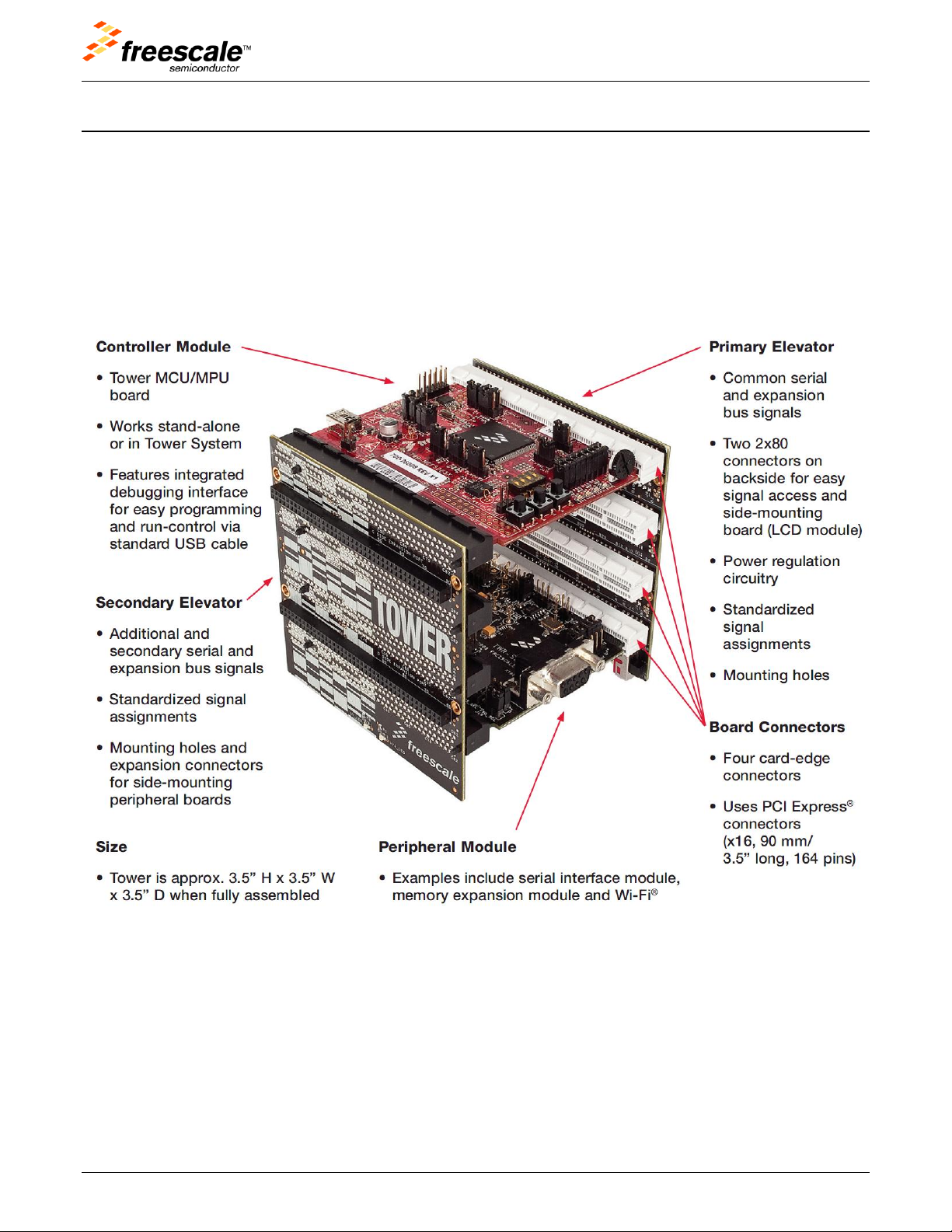
Tower peripheral modules to create development platforms for a wide variety of applications. Figure 1
provides an overview of the Freescale Tower System.
Figure 1. Freescale Tower System Overview
TWRS08UNIVUM TWR-S08UNIV User's Manual Page 4 of 16
1.1 Contents
The TWR-S08UNIV contents include:
TWR-S08UNIV board assembly
3ft USB cable
Interactive DVD with software installers and documentation
Quick Start Guide
The TWR-S08UNIV-DEMO contains:
TWR-RS08DC-KA8
TWR-S08DC-AC60
TWR-S08DC-QD4
TWR-S08DC-QE64
TWR-S08DC-QG8
TWR-S08DC-SH8
1.2 Features
Figure 2 and Figure 3 show the TWR-S08UNIV with some of the key features called out. The following
list summarizes the features of the TWR-S08UNIV Tower Module:
Tower compatible universal board module
Interchangeable Daughter Card Sockets for many S08/RS08 microcontrollers
Touch Tower Plug-in Socket
Touch Sense Tower Plug-in (TWRPI) socket
General purpose Tower Plug-in (TWRPI) socket
On-board OSBDM debug circuit (OSBDM) with virtual serial port
One (1) user-controllable RGB LED
Two (2) user pushbutton switches
Potentiometer
One (1) user-controllable buzzer
TWRS08UNIVUM TWR-S08UNIV User's Manual Page 5 of 16

Figure 2. Callouts on the TWR-S08UNIV
Figure 3. Callouts on TWR-S08UNIV Daughter Cards
TWRS08UNIVUM TWR-S08UNIV User's Manual Page 6 of 16

2. Getting Started
Follow the Quick Start Guide found printed in the TWR-S08UNIV box or the interactive DVD for the list
of recommended steps for getting started. There are also lab walk-through guides available on the
tool support page for the TWR-S08UNIV:
http://www.freescale.com/webapp/sps/site/prod_summary.jsp?code=TWR-S08UNIV.
2.1 Reference Documents
The documents listed below should be referenced for more information on the Kinetis family, Tower
System, and MCU Modules. These can be found in the documentation section of the TWR-S08UNIV
tool support page (http://www.freescale.com/webapp/sps/site/prod_summary.jsp?code=TWR-
S08UNIV).
TWR-S08UNIV-QSG: Quick Start Guide
TWR- S08UNIV -SCH: Schematics
TWR- S08DC-AC60: Schematics
TWR- S08DC-QE64: Schematics
TWR- S08DC-SH8: Schematics
TWR- S08DC-QG8: Schematics
TWR- S08DC-QD4: Schematics
TWR- RS08DC-KA8: Schematics
TWR- S08UNIV-DC Master Pinout
Tower Configuration Tool
3. Hardware Description
The TWR-S08UNIV is a Tower Controller Module featuring a very easy way to switch between different
S08/RS08 MCUs. The TWR-S08UNIV module can be used in stand-alone mode or connected to the
Tower System. The TWR-S08UNIV module must have a Daughter Card TWR-S08DC-XXX plugged in to
operate properly. Each TWR-S08DC-XXX daughter card will have a unique ID associated with the MCU
on the daughter card. Each 5V MCU daughter card will have the option to select between 3V and 5V
setting, which will control the system voltage on the TWR-S08UNIV module. Figure 4 shows a block
diagram of the TWR-S08UNIV. The following sections describe the hardware in more detail.
TWRS08UNIVUM TWR-S08UNIV User's Manual Page 7 of 16

Figure 4. TWR-S08UNIV Block Diagram
3.1 Daughter Cards TWR-S08DC-XXX for the TWR-S08UNIV Module
The TWR-S08UNIV module features a universal socket in the middle of the board which can be
interchanged with several of the TWR-S08DC-XXX.
TWRS08UNIVUM TWR-S08UNIV User's Manual Page 8 of 16

The TWR-S08UNIV-DEMO kit features:
One MC9S08AC60 single MCU with a hardware unique ID for this daughter card
One MC9S08QE64 single MCU with a hardware unique ID for this daughter card
One MC9S08SH8 single MCU with a hardware unique ID for this daughter card
One MC9S08QG8 single MCU with a hardware unique ID for this daughter card
One MC9S08QD4 single MCU with a hardware unique ID for this daughter card
One MC9RS08KA8 single MCU with a hardware unique ID for this daughter card
3.2 System Power
In stand-alone operation, the main power source for the TWR-S08UNIV module is derived from the
5.0V input from either the USB mini-B connector, or the debug header, J12-45. A low-dropout
regulator provides a 3.3V supply from the 5.0V input voltage. Refer to sheet 4 of the TWR-S08UNIV
schematics for more details.
When installed into a Tower System, the TWR-S08UNIV can be powered from either an on-board
source or from another source in the assembled Tower System. If both the on-board and off-board
sources are available, the TWR-S08UNIV will default to the off-board source.
3.2.1 TWR-S08DC-XXX Daughter Cards 3V/5V Switch
The 3V/5V switch allows the daughter card to control the voltage supply to the TWR-S08UNIV module.
The daughter cards without the 3V/5V switch are hard wired to a 3.3V supply voltage to the TWRS08UNIV module. These are the selected daughter cards with the 3V/5V switch:
TWR-S08DC-AC60
TWR-S08DC-SH8
TWR-S08DC-QD4
TWR-RS08DC-KA8
3.3 Debug Interface
There are two debug interface options provided: the on-board OSBDM circuit and an external 6-pin
interface header for the P&E Microsystems Multilink tools.
3.3.1 OSBDM
An on-board MC9S08JM60 based Open Source Background Debug (OSBDM) circuit provides an OSBDM
debug interface to the MCUs. A standard USB A male to Mini-B male cable (provided) can be used for
debugging via the USB connector, J10. The OSBDM interface also provides a USB to serial bridge.
Drivers for the OSJTAG interface are provided in the P&E Micro Tower Toolkit (available on the
included DVD and from P&E at http://www.pemicro.com/osbdm).
Note: The port pin PTE0 (TXD1) connected to the OSBDM USB-to-serial bridge is also connected the
TWR-ELEV and the J12 Header. Refer to 0 “header J12.” and Table 5 “TWR-S08UNIV DIP Switch Table”
for more information.
TWRS08UNIVUM TWR-S08UNIV User's Manual Page 9 of 16

Pin
Function
TWR-S08UNIV Connection
1
BGND
3.3V MCU supply (P3V3_MCU)
2
GND
GND
3
NC
No Connection
4
nRESET
nRESET
5
NC
No Connection
6
VDD
3Vor 5V, depending on the daughter card switch position
Left-side 2x10 Connector
Right-side 2x10 Connector
Pin
Description
1
5V VCC
2
3.3 V VCC
3
GND
4
3.3V VDDA
5
VSS (Analog GND)
6
VSS (Analog GND)
7
VSS (Analog GND)
8
ADC: Analog 0
9
ADC: Analog 1
10
VSS (Analog GND)
11
VSS (Analog GND)
12
ADC: Analog 2
13
VSS (Analog GND)
14
VSS (Analog GND)
Pin
Description
1
GND
2
GND
3
I2C: SCL
4
I2C: SDA
5
GND
6
GND
7
GND
8
GND
9
SPI: MISO
10
SPI: MOSI
11
SPI: SS
12
SPI: CLK
13
GND
14
GND
3.3.2 BDM Multilink 6-PIN
The BDM Multilink is a 6-pin (3x2) connector (0.1"Pitch, 0.1” Row) connector providing access to the
target daughter card MCU to program and debug the microcontroller. The BDM Multilink 6-pin
connections to the debug connector, J9, are shown in Table 1.
Table 1. BDM Multilink 6-PIN Connector Pinout
3.4 Potentiometer, Pushbuttons, LEDs, Beeper
The TWR-S08UNIV features two pushbutton switches connected to GPIO/interrupt signals, one RGB
(red, green, blue) LED connected to GPIO, and a potentiometer connected to an ADC input signal, and
a beeper connected to a timer channel. Refer to Section 6 “Input/Output Connections for Daughter
Cards” for information about which port pins are connected to these features.
3.5 General Purpose Tower Plug-in (TWRPI) Socket
The TWR-S08UNIV features a General Purpose TWRPI socket that can accept a variety of different
Tower Plug-in modules featuring sensors, RF transceivers, accelerometers, and more. The General
Purpose TWRPI socket provides access to I2C, SPI, IRQs, GPIOs, timers, analog conversion signals, and
voltage supplies. The pinout for the TWRPI Socket is defined in Table 2.
Refer to Section 6 “Input/Output Connections for Daughter Cards” for the specific TWR-S08UNIV pin
connections to the General Purpose TWRPI socket.
Table 2. General Purpose TWRPI socket pinout
TWRS08UNIVUM TWR-S08UNIV User's Manual Page 10 of 16

15
GND
16
GND
17
NC
18
NC
19
GND
20
NC 15
GPIO: GPIO0/IRQ
16
GPIO: GPIO1/IRQ
17
GPIO: GPIO2
18
GPIO: GPIO3
19
GPIO: GPIO4/Timer
20
GPIO: GPIO5/Timer
Pin
Description
1
5V VCC
2
3.3 V VCC
3
Electrode 0
4
3.3V VDDA
5
Electrode 1
6
VSS (Analog GND)
7
Electrode 2
8
Electrode 3
9
Electrode 4
10
Electrode 5
11
Electrode 6
12
Electrode 7
13
Electrode 8
14
Electrode 9
15
Electrode 10
16
Electrode 11
17
NC
18
NC
19
GND
20
NC
3.6 Touch Pad Tower Plug-in (TWRPI) Socket
There are twelve electrodes GPIO inputs are connected to a Touch Tower Plug-in (TWRPI) socket that
can accept Touch TWRPI daughter cards that may feature keypads, rotary dials, sliders, etc.
The pinout for the Touch Pad TWRPI socket is defined in Table 3. Refer to Section 6 “Input/Output
Connections for Daughter Cards” for the specific TWR-S08UNIV pin connections to the Touch TWRPI
socket.
Table 3. Touch Pad TWRPI socket pinout
3.7 Touch Sensor Tower Plug-in (TWRPI) TWRPI
The TWR-S08UNIV features a Touch Sensor TWRPI socket that can accept a variety of different Tower
Plug-in modules featuring the MPR031 and MPR121 Touch sensors, and TSS software using GPIO. The
pinout for the Touch Sensor TWRPI Socket is defined in Table 24.
TWRS08UNIVUM TWR-S08UNIV User's Manual Page 11 of 16

Left-side 2x10 Connector
Right-side 2x10 Connector
Pin
Description
1
5V VCC
2
3.3 V VCC
3
Electrode IN 0
4
3.3V VDDA
5
Electrode IN 1
6
VSS (Analog GND)
7
Electrode IN 2
8
Electrode IN 3
9
Electrode IN 4
10
Electrode IN 5
11
Electrode IN 6
12
Electrode IN 7
13
Electrode IN 8
14
Electrode IN 9
15
Electrode IN 10
16
Electrode IN 11
17
NC
18
NC
19
GND
20
NC
Pin
Description 1 GND
2
GND
3
I2C: SCL
4
I2C: SDA
5
Electrode OUT 0
6
Electrode OUT
7
Electrode OUT
8
Electrode OUT
9
Electrode OUT
10
Electrode OUT
11
Electrode OUT
12
Electrode OUT
13
Electrode OUT
14
Electrode OUT
15
Electrode OUT
16
Electrode OUT
17
GPIO: GPIO0/IRQ
18
NC
19
NC
20
GND
Table 4. Touch Sensor TWRPI socket pinout
4. Software - CodeCreator
The CodeCreater Software is a quick and easy to use GUI, which allows one to create an RS08/S08
peripheral module “C” code example, in under 10 seconds. This demonstration RS08/S08 code can
then be loaded into the selected TWR-S08DC-XXX daughter card board.
Download and unzip the “FREESCALE_CODECREATOR_V15” from the web.
http://www.freescale.com/webapp/sps/site/prod_summary.jsp?code=TWR-S08UNIV
TWRS08UNIVUM TWR-S08UNIV User's Manual Page 12 of 16

Jumper
Feature
Switch
Setting
Pin Function
SW1-1**
RXD connection to
Target MCU, J3-38
ON
OFF*
RXD connection from Header J12-44
Connection OPEN
SW1-2**
RXD connection to
Target MCU, J3-38
ON*
OFF
TXD connection from JM60 OSBDM Virtual
COM Port
Connection CLOSED
SW1-3**
RXD connection to
Target MCU, J3-38
ON
OFF*
RXD connection from Elevator A41
Connection OPEN
SW1-4
SPI Chip Select to
TWR-Elevators
ON
OFF*
SPI1 CS0
Connection OPEN
SW1-5
SPI Chip Select to
TWR-Elevators
ON
OFF*
SPI1 CS1
Connection OPEN
Step 1. Step 2.
Launch the CC15.exe. Select the MCU, Module, and enter a Project Name.
Then hit “Build CW6.3 Project”.
Step 3.
Import project into CW10.1 using the “Import CodeWarrior Classic” or double-click on the
<example>.mcp file in the created project were CC15.exe is located.
5. DIP Switch Table
There are dip switch settings on the TWR-S08UNIV board that provide configuration for the RXD
connection to the MCU, SPI Chip Select (CS), and reprogramming the JM60 OSBDM Firmware. Refer to
the following table for details. The default DIP switch settings are shown in bold with asterisks.
Table 5. TWR-S08UNIV DIP Switch Table
TWRS08UNIVUM TWR-S08UNIV User's Manual Page 13 of 16

Jumper
Feature
Switch
Setting
Pin Function
SW1-6
SPI Chip Select to
TWR-Elevators
ON
OFF*
SPI0 CS0
Connection OPEN
SW1-7
SPI Chip Select to
TWR-Elevators
ON
OFF*
SPI0 CS1
Connection OPEN
SW1-8
OSBDM Bootloader
Enable/Disable
ON
OFF*
ON=JM60 in Bootloader mode, OFF=normal
Connection OPEN
Pin #
Side B
Pin #
Side A
Name
Usage
Name
Usage
B1
5V
5.0V Power
A1
5V
5.0V Power
B2
GND
Ground
A2
GND
Ground
B3
3.3V
3.3V Power
A3
3.3V
3.3V Power
B4
NC
NC
A4
NC
NC
B5
GND
Ground
A5
GND
Ground
B6
GND
Ground
A6
GND
Ground
B7
ELE_SCLK
J3-2
A7
ELE_SCL
J3-4
B8
ELE_SDHC__CS1
J3-49
A8
ELE_SDA
J3-3
B9
ELE_SDHC__CS0
J3-49
A9
NC
NC
B10
ELE_MOSI
J3-1
A10
NC
NC
B11
ELE_MISO
J3-50
A11
NC
NC
B12
NC
NC
A12
NC
NC
B13
NC
NC
A13
NC
NC
B14
NC
NC
A14
NC
NC
B15
NC
NC
A15
NC
NC
B16
NC
NC
A16
NC
NC
B17
NC
NC
A17
NC
NC
B18
NC
NC
A18
NC
NC
B19
NC
NC
A19
NC
NC
*Default Factory Setting
**Only one of the three SW1-1, SW1-2, and SW1-3 connections should be ON.
6. Input/Output Connections for Daughter Cards
All of the input/output signals from all of the daughter cards are available on the header J12. Please
refer to the document “TWR-S08UNIV-DC MASTER_PINOUT.pdf” available on the Freescale website:
http://www.freescale.com/webapp/sps/site/prod_summary.jsp?code=TWR-S08UNIV
7. Tower Elevator Connections
The TWR-S08UNIV features two expansion card-edge connectors that interface to the Primary and
Secondary Elevator boards in a Tower system. The Primary Connector (comprised of sides A and B) is
utilized by the TWR-S08UNIV while the Secondary Connector (comprised of sides C and D) only makes
connections to the GND pins. Table 6 provides the pinout for the Primary Connector.
Table 6. TWR-S08UNIV Primary Connector Pinout
TWRS08UNIVUM TWR-S08UNIV User's Manual Page 14 of 16

Pin #
Side B
Pin #
Side A
Name
Usage
Name
Usage
B20
NC
NC
A20
NC
NC
B21
NC
NC
A21
NC
NC
B22
NC
NC
A22
NC
NC
B23
NC
NC
A23
NC
NC
B24
NC
NC
A24
NC
NC
B25
NC
NC
A25
NC
NC
B26
GND
Ground
A26
GND
Ground
B27
NC
NC
A27
NC
NC
B28
NC
NC
A28
ELE_ANA2
J3-27
B29
NC
NC
A29
ELE_ANA1
J3-28
B30
NC
NC
A30
ELE_ANA0
J3-29
B31
GND
Ground
A31
GND
Ground
B32
NC
NC
A32
NC
NC
B33
NC
NC
A33
ELE_GPIO5TPM
J3-42
B34
NC
NC
A34
ELE_GPIO4TPM
J3-67
B35
NC
NC
A35
NC
NC
B36
3.3V
3.3V Power
A36
3.3V
3.3V Power
B37
NC
NC
A37
NC
NC
B38
NC
NC
A38
NC
NC
B39
NC
NC
A39
NC
NC
B40
NC
NC
A40
NC
NC
B41
NC
NC
A41
RXD_ELEV
J3-38
B42
NC
NC
A42
TXD_ELEV
J3-37
B43
NC
NC
A43
NC
NC
B44
ELE_MISO
J3-50
A44
NC
NC
B45
ELE_MOSI
J3-1
A45
NC
NC
B46
ELE_SPI_CS0
J3-49
A46
NC
NC
B47
ELE_SPI_CS1
J3-49
A47
NC
NC
B48
ELE_SCLK
J3-2
A48
NC
NC
B49
GND
Ground
A49
GND
Ground
B50
ELE_SCL
J3-4
A50
NC
NC
B51
ELE_SDA
J3-3
A51
NC
NC
B52
NC
NC
A52
NC
NC
B53
NC
NC
A53
NC
NC
B54
NC
NC
A54
NC
NC
B55
NC
NC
A55
NC
NC
B56
NC
NC
A56
NC
NC
B57
NC
NC
A57
NC
NC
B58
NC
NC
A58
NC
NC
B59
NC
NC
A59
NC
NC
B60
NC
NC
A60
NC
NC
B61
NC
NC
A61
NC
NC
B62
NC
NC
A62
NC
NC
B63
NC
NC
A63
GPIO_TPM_RSTO
J3-68
B64
NC
NC
A64
NC
NC
B65
GND
Ground
A65
GND
Ground
B66
NC
NC
A66
NC
NC
B67
NC
NC
A67
NC
NC
TWRS08UNIVUM TWR-S08UNIV User's Manual Page 15 of 16

Pin #
Side B
Pin #
Side A
Name
Usage
Name
Usage
B68
NC
NC
A68
NC
NC
B69
NC
NC
A69
NC
NC
B70
NC
NC
A70
NC
NC
B71
NC
NC
A71
NC
NC
B72
NC
NC
A72
NC
NC
B73
NC
NC
A73
NC
NC
B74
NC
NC
A74
NC
NC
B75
NC
NC
A75
NC
NC
B76
NC
NC
A76
NC
NC
B77
NC
NC
A77
NC
NC
B78
NC
NC
A78
NC
NC
B79
NC
NC
A79
NC
NC
B80
NC
NC
A80
NC
NC
B81
GND
Ground
A81
GND
Ground
B82
3.3V
3.3V Power
A82
3.3V
3.3V Power
TWRS08UNIVUM TWR-S08UNIV User's Manual Page 16 of 16
 Loading...