

Page 1

TWR-P1025 Tower Module
Hardware User Guide
TWR-P1025HUG
Rev. 0, 3/2012
Page 2

How to Reach Us:
Home Page:
www.freescale.com
Web Support:
http://www.freescale.com/support
USA/Europe or Locations Not Listed:
Freescale Semiconductor, Inc.
Technical Information Center, EL516
2100 East Elliot Road
Tempe, Arizona 85284
+1-800-521-6274 or
+1-480-768-2130
www.freescale.com/support
Europe, Middle East, and Africa:
Freescale Halbleiter Deutschland GmbH
Technical Information Center
Schatzbogen 7
81829 Muenchen, Germany
+44 1296 380 456 (English)
+46 8 52200080 (English)
+49 89 92103 559 (German)
+33 1 69 35 48 48 (French)
www.freescale.com/support
Japan:
Freescale Semiconductor Japan Ltd.
Headquarters
ARCO Tower 15F
1-8-1, Shimo-Meguro, Meguro-ku
Tokyo 153-0064
Japan
0120 191014 or
+81 3 5437 9125
support.japan@freescale.com
Asia/Pacific:
Freescale Semiconductor China Ltd.
Exchange Building 23F
No. 118 Jianguo Road
Chaoyang District
Beijing 100022
China
+86 010 5879 8000
support.asia@freescale.com
Information in this document is provided solely to enable system and software
implementers to use Freescale Semiconductor products. There are no express or
implied copyright licenses granted hereunder to design or fabricate any integrated
circuits or integrated circuits based on the information in this document.
Freescale Semiconductor reserves the right to make changes without further notice to
any products herein. Freescale Semiconductor makes no warranty, representation or
guarantee regarding the suitability of its products for any particular purpose, nor does
Freescale Semiconductor assume any liability arising out of the application or use of
any product or circuit, and specifically disclaims any and all liability, including without
limitation consequential or incidental damages. “Typical” parameters which may be
provided in Freescale Semiconductor data sheets and/or specifications can and do
vary in different applications and actual performance may vary over time. All operating
parameters, including “Typicals” must be validated for each customer application by
customer’s technical experts. Freescale Semiconductor does not convey any license
under its patent rights nor the rights of others. Freescale Semiconductor products are
not designed, intended, or authorized for use as components in systems intended for
surgical implant into the body, or other applications intended to support or sustain life,
or for any other application in which the failure of the Freescale Semiconductor product
could create a situation where personal injury or death may occur. Should Buyer
purchase or use Freescale Semiconductor products for any such unintended or
unauthorized application, Buyer shall indemnify and hold Freescale Semiconductor
and its officers, employees, subsidiaries, affiliates, and distributors harmless against all
claims, costs, damages, and expenses, and reasonable attorney fees arising out of,
directly or indirectly, any claim of personal injury or death associated with such
unintended or unauthorized use, even if such claim alleges that Freescale
Semiconductor was negligent regarding the design or manufacture of the part.
Freescale and the Freescale logo are trademarks of Freescale
Semiconductor, Inc., Reg. U.S. Pat. & Tm. Off. QUICC Engine is trademarks
of Freescale Semiconductor, Inc. All other product or service names are the
property of their respective owners.
© Freescale Semiconductor, Inc., 2012
Document Number: TWR-P1025HUG
Rev. 0, 3/2012
Page 3

Contents
Paragraph
Number Title
Page
Number
Chapter 1
TWR-P1025 Overview
1.1 Introduction...................................................................................................................... 1-1
1.2 Contents ........................................................................................................................... 1-2
1.3 Features............................................................................................................................ 1-2
1.4 Getting Started ................................................................................................................. 1-4
1.5 Reference Documents ...................................................................................................... 1-4
Chapter 2
Power Requirements
2.1 Overview.......................................................................................................................... 2-1
Chapter 3
Hardware Description
3.1 P1025 Microprocessor ..................................................................................................... 3-1
3.2 Clocking........................................................................................................................... 3-2
3.3 System Power .................................................................................................................. 3-5
3.4 Debug Interface................................................................................................................ 3-5
3.5 Accelerometer.................................................................................................................. 3-5
3.6 Pushbutton and LEDs ...................................................................................................... 3-5
3.7 Ethernet............................................................................................................................ 3-5
3.8 USB.................................................................................................................................. 3-7
3.9 Micro Secure Digital Card Slot (micro SDHC)............................................................... 3-8
3.10 Local Bus Interface .......................................................................................................... 3-8
3.11 UART ............................................................................................................................... 3-8
3.12 I2C ................................................................................................................................... 3-9
3.13 SPI.................................................................................................................................... 3-9
3.14 DDR3 ............................................................................................................................... 3-9
3.15 GPIO & Interrupts ......................................................................................................... 3-12
4.1 P1025 Jumper Table......................................................................................................... 4-1
Freescale Semiconductor iii
Chapter 4
Switch Table
TWR-P1025 Hardware User Guide, Rev. 0
Page 4

Contents
Paragraph
Number Title
Page
Number
Chapter 5
Input/Output Connectors and Pin Usage Table
5.1 LED Usage....................................................................................................................... 5-1
5.2 I/O Connectors and Pin Usage Table ............................................................................... 5-1
Chapter 6
Tower Elevator Connections
6.1 Overview.......................................................................................................................... 6-1
Appendix A
Revision History
A.1 Version Number 0 ............................................................................................................ 7-1
iv Freescale Semiconductor
TWR-P1025 Hardware User Guide, Rev. 0
Page 5

Figures
Figure
Number Title
Page
Number
1-1 Freescale Tower System.......................................................................................................... 1-1
1-2 Callouts on front side of the TWR-P1025 .............................................................................. 1-3
1-3 Callouts on back side of the TWR-P1025............................................................................... 1-3
2-1 Power Supply Barrel Connector (J2) Polarity......................................................................... 2-1
3-1 TWR-P1025 Block Diagram................................................................................................... 3-1
3-2 P1025 Clocking Scheme ......................................................................................................... 3-3
3-3 eTSEC connection to AR8035 PHY....................................................................................... 3-6
3-4 NOR Local Bus Connection ................................................................................................... 3-8
Freescale Semiconductor v
TWR-P1025 Hardware User Guide, Rev. 0
Page 6

Tables
Table
Number Title
Tables
Page
Number
2-1 Power Distribution Summary.................................................................................................. 2-1
3-1 P1025 CCB to SYSCLK Ratio Selection ............................................................................... 3-4
3-2 P1025 e500 Core 0 & 1 to CCB Clock Ratio Selection.......................................................... 3-4
3-3 P1025 DDR Clock PLL Ratio................................................................................................. 3-4
3-4 CPU Speed Selection .............................................................................................................. 3-5
3-5 eTSEC1 PHY Connectivity .................................................................................................... 3-6
3-6 eTSEC1 PHY Connectivity .................................................................................................... 3-7
3-7 I2C1 Connectivity ................................................................................................................... 3-9
3-8 I2C2 Connectivity ................................................................................................................... 3-9
3-9 DDR3 Signals ....................................................................................................................... 3-10
3-10 P1025 Interrupt Usage .......................................................................................................... 3-13
3-11 P1025 GPIO Usage ............................................................................................................... 3-13
4-1 P1025 Jumper Table................................................................................................................ 4-1
5-1 LED Usage Table .................................................................................................................... 5-1
5-2 I/O Connectors and Pin Usage Table ...................................................................................... 5-1
6-1 TWR-P1025 Primary Connector Pinout ................................................................................. 6-1
6-2 TWR-P1025 Primary Connector Pinout ................................................................................. 6-4
Freescale Semiconductor vii
TWR-P1025 Hardware User Guide, Rev. 0
Page 7
Chapter 1
TWR-P1025 Overview
1.1 Introduction
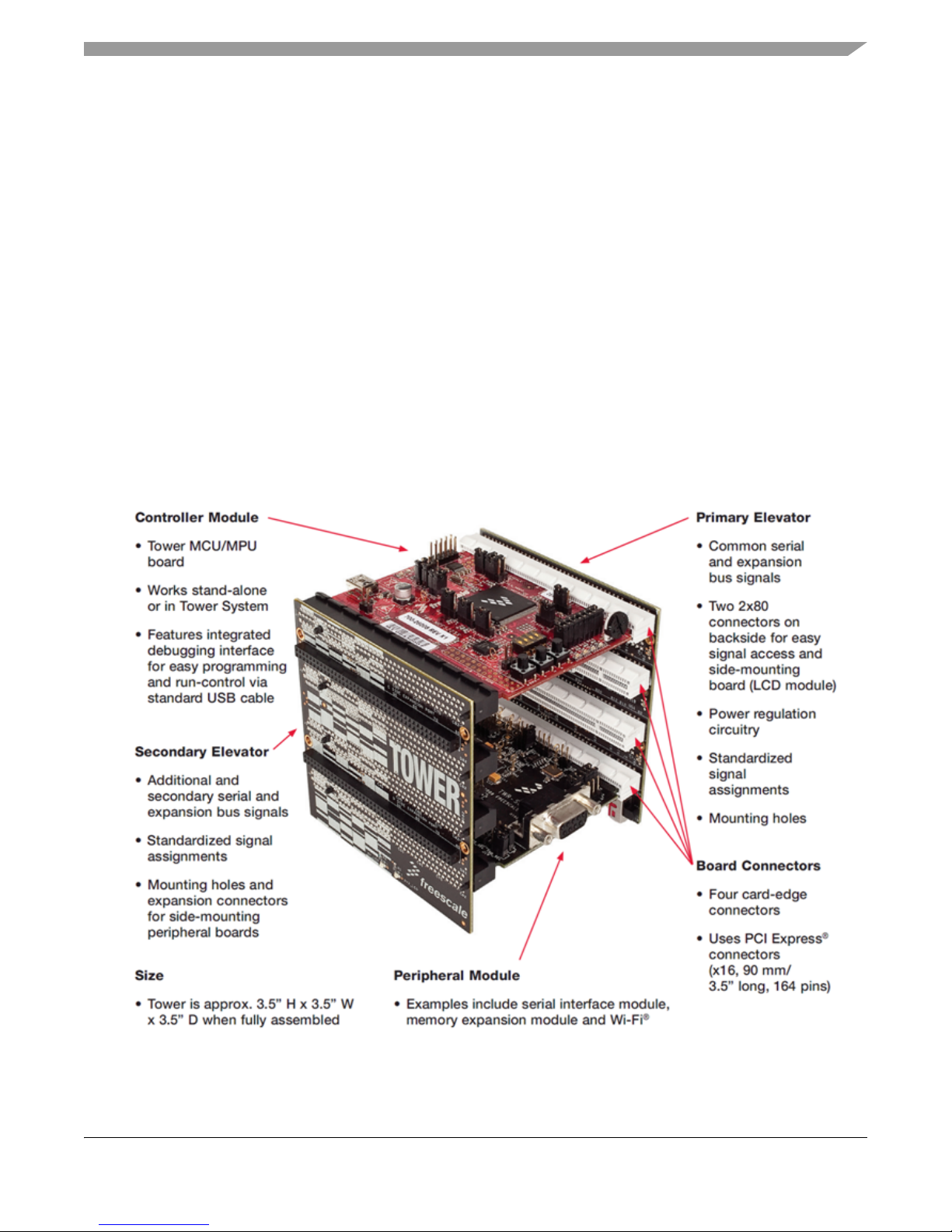
The TWR-P1025 is a Tower Controller Module compatible with the Freescale Tower System. It can
function as a stand-alone, low-cost platform for the evaluation of the QorIQ P1xxx family of
microprocessor (MPU) devices. The TWR-P1025 features the QorIQ P1025 dual core processor based on
the PowerPC® e500 core architecture.
The TWR-P1025 is available as a stand-alone product or can be combined with the Tower Elevator
Modules (TWR-ELEV) and other Tower eco-system components to create development platforms for a
wide variety of applications. Figure 1-1 shows an overview of the Freescale Tower System.
Freescale Semiconductor 1
Figure 1-1. Freescale Tower System
TWR-P1025 Hardware User Guide, Rev. 0
Page 8

TWR-P1025 Overview
1.2 Contents
The TWR-P1025 contents include:
• TWR-P1025 board
• Quick Start Guide
1.3 Features
The features of the TWR-P1025 Tower MPU Module:
• Tower compatible microprocessor module
• Dual core P1025 in a 561 TEPBGA package operating up to 533 MHz
• P1025 JTAG
•CPLD JTAG
• Three axis accelerometer (MMA8451Q)
• Two (2) user-controllable LEDs
• One (1) reset pushbutton switch
• Ten-way DIP Switch for configuration
• microSD card slot
• mini-PCIe slot
• Two (2) 10/100/1000Mbps Ethernet RJ45
• Two (2) USB2.0 Type A
• One (1) mini-USB TypeB dual UART
• 512 MB DDR3@667 MHz
• 64 MB Flash
• IEEE1588 pinned to header + DAC and VXCO (DNP option)
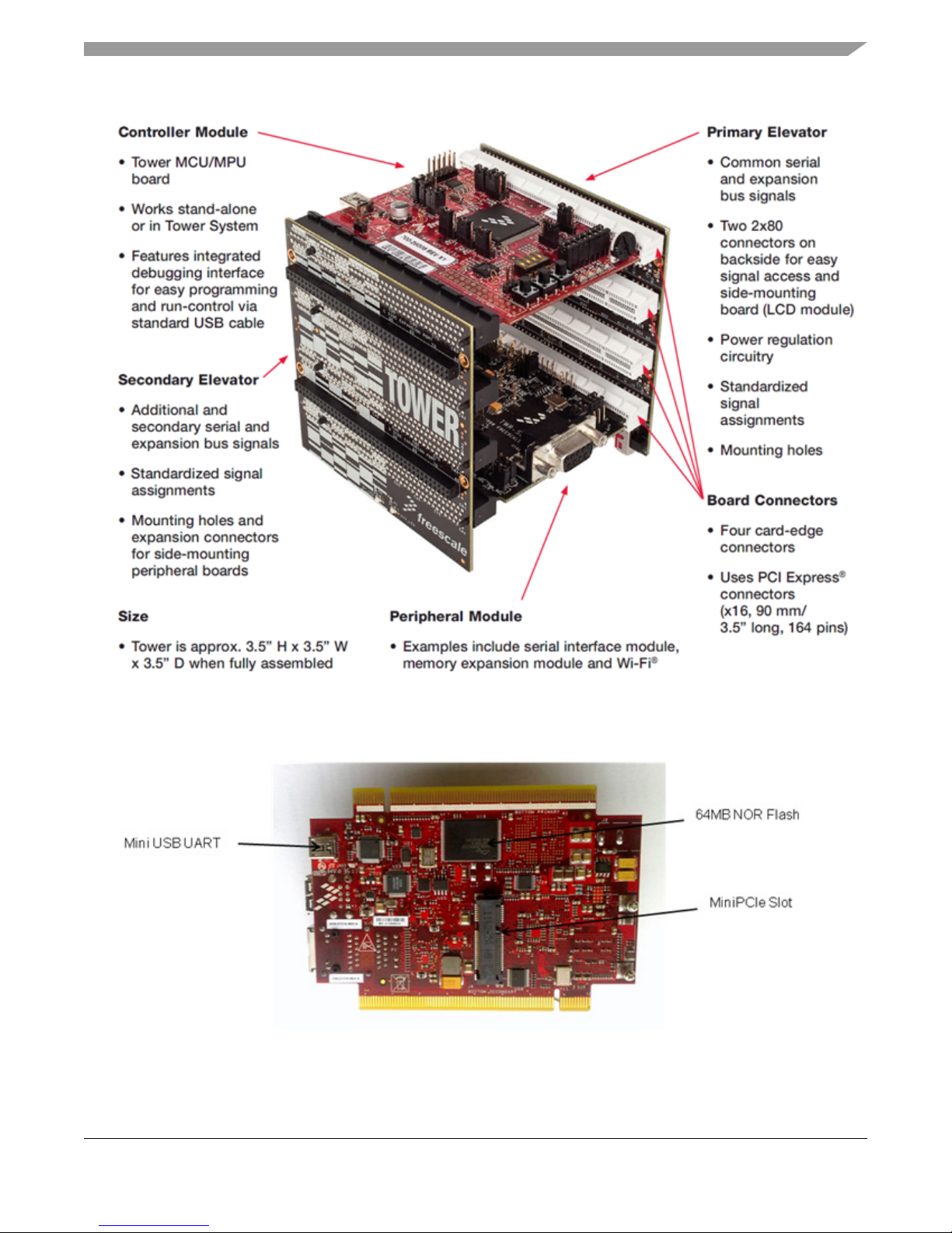
Figure 1-2 and Figure 1-3 show the TWR-P1025 with some of the key features.
2 Freescale Semiconductor
TWR-P1025 Hardware User Guide, Rev. 0
Page 9
TWR-P1025 Overview
Figure 1-2. Callouts on front side of the TWR-P1025
Figure 1-3. Callouts on back side of the TWR-P1025
TWR-P1025 Hardware User Guide, Rev. 0
Freescale Semiconductor 3
Page 10

TWR-P1025 Overview
1.4 Getting Started
Follow the printed Quick Start Guide or the interactive DVD contained in the TWR-P1025 box for
recommended get started steps.
1.5 Reference Documents
For more information on the QorIQ family, Tower System, and MPU Modules refer following documents:
• TWR-P1025-QSG: Quick Start Guide
• TWR-P1025-SCH: Schematics
• TWR-P1025-PWA: Design Package
• P1025 Reference Manual
4 Freescale Semiconductor
TWR-P1025 Hardware User Guide, Rev. 0
Page 11
Chapter 2
Power Requirements
2.1 Overview
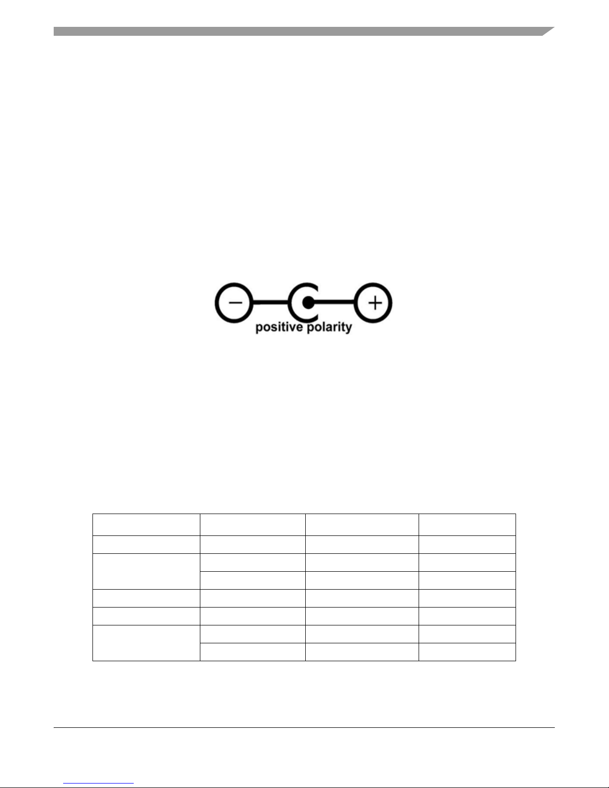
The TWR-P1025 is designed to be externally powered through barrel connector J2 from a 5V@5A DC
supply. The barrel connector is manufactured by SWITCHCRAFT with part number RAPC722X. The
mating plug should have an inner diameter of 2.1mm and outer diameter of 5.5mm. Figure 2-1 shows the
polarity of the barrel connector.
Figure 2-1. Power Supply Barrel Connector (J2) Polarity
The 5V input is used to generate all voltages on the board. Additionally when used with TWR elevators
and other TWR peripherals, the TWR-P1025 provides 5V and 3.3V supplies.
There are several expansion options on the board that allow external boards to interface to the
TWR-P1025, such as the mini PCIe connector, USB ports and elevator expansion. As these plug in cards
have variable power requirements as well as numerous population combinations the Power capability of
the different expansion interfaces and the core board are listed in Ta bl e 2-1 . Consideration of total available
power from the external supply should be considered when adding plug-in devices or using the elevator
expansion.
Main Board 5 2.5A
MiniPCIe 3.3 1A
USB Port 1 5 0.5
USB Port 2 5 0.5
ELEVATORS 5 0.5
Freescale Semiconductor 1
Table 2-1. Power Distribution Summary
Voltage (V) Current (A) Comment
1.5 0.5
3.3 0.5
TWR-P1025 Hardware User Guide, Rev. 0
Page 12
Chapter 3
Hardware Description
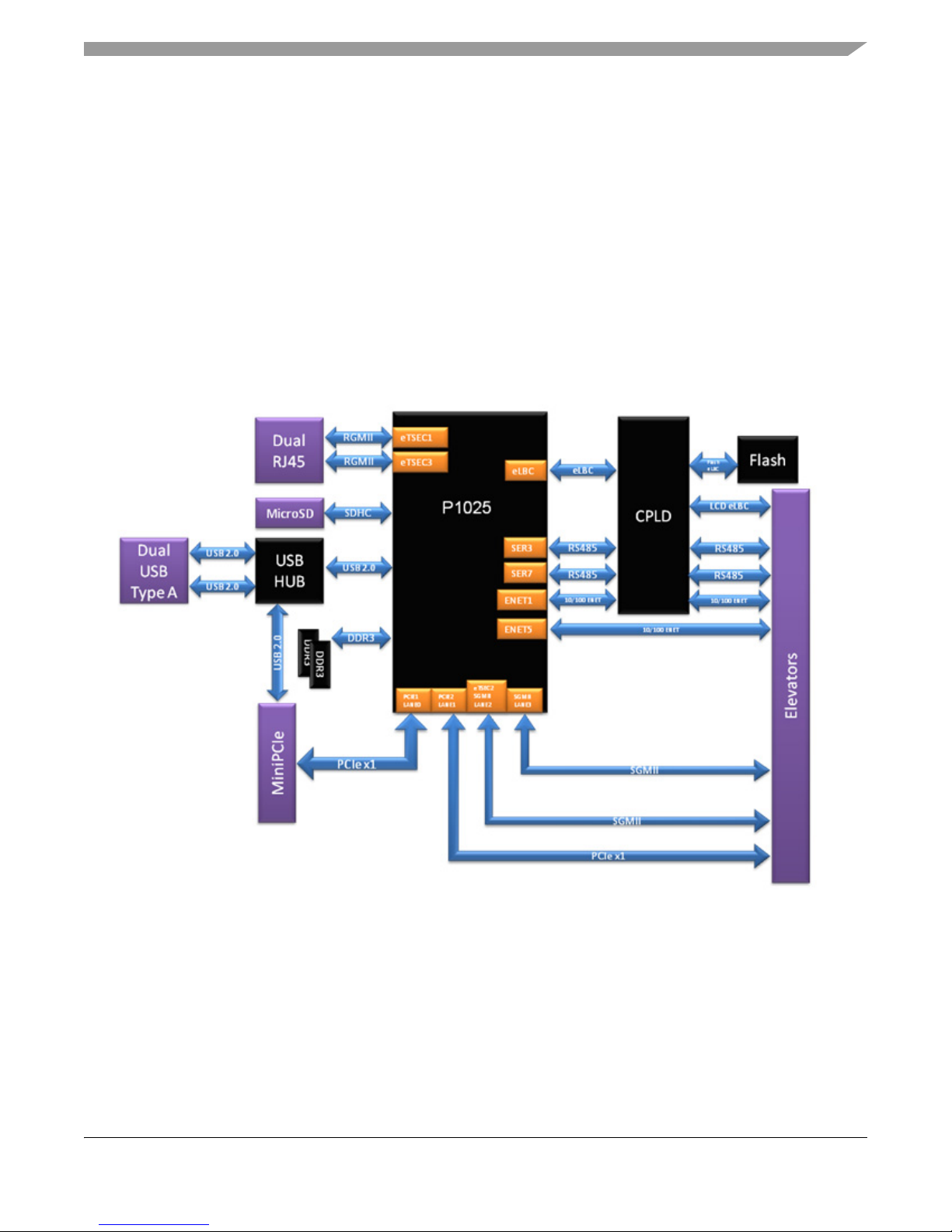
The TWR-P1025 is a Tower Controller Module featuring the P1025-a dual core e500v2 based
microprocessor in a 561 TEPBGA package with a maximum core operating frequency of 533MHz. It is
intended to be used stand-alone or in the Freescale Tower System. Power is supplied through a 5V barrel
connector. Figure 3-1 shows a block diagram of the TWR-P1025. The following sections describe the
hardware in more detail.
3.1 P1025 Microprocessor
The TWR-P1025 module features the P1025, the key features are:
• 533 MHz maximum core operating frequency
• 561 TEPBGA, 23mm x 23mm, 1.0mm pitch package
Freescale Semiconductor 1
Figure 3-1. TWR-P1025 Block Diagram
TWR-P1025 Hardware User Guide, Rev. 0
Page 13

Hardware Description
• Dual high-performance 32-bit cores, built on Power Architecture® technology:
— 32-bit e500v2 PowerPC core
— 36-bit physical addressing
— Double-precision floating-point support
— 32 Kbyte L1 instruction cache and 32 Kbyte L1 data cache for each core
— 400 MHz to 533 MHz clock frequency
• 256 Kbyte L2 cache with ECC. Also configurable as SRAM and stashing memory.
• Three 10/100/1000 Mbps enhanced three-speed Ethernet controllers (eTSECs)
— TCP/IP acceleration, quality of service, and classification capabilities
— IEEE® 1588 support
— Lossless flow control
— MII, RMII, RGMII, SGMII
• High-speed interfaces supporting various multiplexing options:
— Four SerDes upto 2.5 GHz/lane multiplexed across controllers
— Two PCI Express interfaces
— Two SGMII interfaces
• High-speed USB controller (USB 2.0)
— Host and device support
— Enhanced host controller interface (EHCI)
— ULPI interface to PHY
• Enhanced secure digital host controller (SD/MMC)
• Enhanced serial peripheral interface (eSPI)
• Integrated security engine
— Protocol support includes ARC4, 3DES, AES, RSA/ECC, RNG, single-pass SSL/TLS
— XOR acceleration
• 32-bit DDR3 SDRAM memory controller with ECC support
• Programmable interrupt controller (PIC) compliant with OpenPIC standard
• One four-channel DMA controller
• Two I2C controllers, DUART, timers
• Enhanced local bus controller (eLBC)
• QUICC Engine block
3.2 Clocking
The P1025 takes a single input clock, SYSCLK, as its primary clock source for the e500 cores and all of
the devices and interfaces that operate synchronously with the core. As shown in Figure 3-1, the SYSCLK
input (frequency) is multiplied up using a phase lock loop (PLL) to create the core complex bus (CCB)
clock (also called the platform clock). The CCB clock is used by virtually all of the synchronous system
logic, including the L2 cache, and other internal blocks such as the DMA and interrupt controller. The CCB
2 Freescale Semiconductor
TWR-P1025 Hardware User Guide, Rev. 0
Page 14

Hardware Description
clock also feeds the PLLs in the e500 core and the PLL that create clocks for the integrated flash controller.
Note that the divide-by-two CCB clock divider and the divide-by-n CCB clock divider, shown in
Figure 3-2, are located in the DDR and IFC blocks, respectively.
A SYSCLK of 66.667 MHz will be the default used for the design. The board has been designed to support
Profibus applications that require 12 Mbps baud rate with 16x oversampling. A 64 MHz oscillator provides
the necessary BRG clock for this bit rate.
The DDR memory controller complex may use the platform clock or the DDRCLK, which is multiplied
up using a separate PLL to create a unique DDR memory controller complex clock. In this case, the DDR
complex operates asynchronous with respect to the platform clock and runs at a fixed data rate of
667MTps.
The clocks for the PCI Express and SGMII interfaces are derived from a PLL in the SerDes block. This
PLL is driven by a reference clock (SD_REF_CLK/SD_REF_CLK) whose input frequency is a function
of the bit rate being used (100 MHz or 125 MHz). Note that for proper PCI Express operation, the CCB
clock frequency must be greater than 62.5 MHz.
The Ethernet blocks operate asynchronously with respect to the rest of the device. These blocks use receive
and transmit clocks supplied by their respective PHY chips, plus a 125-MHz clock input for gigabit
protocols. Data transfers are synchronized to the CCB clock internally.
Table 3- 1 and Ta ble 3- 2 describe the CCB and core platform frequency ratio selection. Ta ble 3 -3 describes
the DDRCLK input ratio to DDR controller clock ratio.
Freescale Semiconductor 3
Figure 3-2. P1025 Clocking Scheme
TWR-P1025 Hardware User Guide, Rev. 0
Page 15

Hardware Description
Two DIP switches (SW1[7:8]) select the core/QE frequencies. Three modes run at 66.667MHz SYSCLK
whereas the 4th mode is for Profibus application and uses the 64 MHz SYSCLK.
The DDR runs at a fixed x10 multiplier to DDR_CLK.
Table 3-1. P1025 CCB to SYSCLK Ratio Selection
Functional Signals Reset Configuration Name Value CCB Clock : SYSCLK Ratio
LA[29:31] No Default cfg_sys_pll[0:2] 000 4:1
001 5:1
010 6:1
Table 3-2. P1025 e500 Core 0 & 1 to CCB Clock Ratio Selection
Functional Signals Reset Configuration
Name
LBCTL, LALE,
LGPL2/LOE/LFRE
No Default
LWE0, UART_SOUT1,
READY_P1
No Default
cfg_core0_pll[0:2]
cfg_core1_pll[0:2]
Table 3-3. P1025 DDR Clock PLL Ratio
Functional Signals
TSEC_1588_CLK_OUT,
TSEC_1588_PULSE_OUT1,
TSEC_1588_PULSE_OUT2
No Default
Reset Configuration
Name
cfg_ddr_pll[0:2] 000 3:1
Val ue
000 Reserved
001 Reserved
010 1:1
011 3:2 (1.5:1)
100 2:1
101 5:2 (2.5:1)
110 3:1
111 Reserved
Value
001 4:1
010 6:1
011 8:1
e500 Core: CCB Clock
Ratio
e500 Core: CCB Clock
Ratio
4 Freescale Semiconductor
100 10:1
101 Reserved
110 Reserved
111 Synchronous mode
TWR-P1025 Hardware User Guide, Rev. 0
Page 16

Table 3-4. CPU Speed Selection
Hardware Description
CPU_SPEED
_SELECT0
SW1.7
ON ON 500 333 66.667
OFF ON 533 266 66.667
ON OFF 400 400 66.667
OFF OFF 384 384 64
CPU_SPEED_SELECT1
SW1.8
CORE(0 &1) Speed
(MHz)
QE Speed (MHz)
SYSCLK (MHz)
3.3 System Power
The TWR-P1025 is powered through a barrel connector that provides 5V to the board (and elevators if
present). All further operating voltages are generated via onboard regulators.
The power supply should be rated at 5V @5A.
3.4 Debug Interface
There are two JTAG connectors on board, one for the P1025 (J3) and another for the CPLD(J1). Both use
standard debuggers available from Freescale and Altera respectively. Pin 1 is marked on both connectors.
Refer to the relevant debug tool for operating instructions.
3.5 Accelerometer
An MMA8451Q digital accelerometer is connected to the P1025 through its second I2C interface at
address 0x1C and the accelerometers INT1 signal routed to the P1025 IRQ0.
3.6 Pushbutton and LEDs
The TWR-P1025 features one pushbutton switch connected to a reset circuit. Pressing this button initiates
the reset sequence in the CPLD and performs a HRESET sequence to the P1025 as well as resetting the
Ethernet PHYs, NOR Flash and USB circuitry.
Two LEDs are available to the user through software control. The P1025 GPIO pins, PB27 and PB31 are
routed through the CPLD to control these two LEDs.
3.7 Ethernet
The connectivity between the P1025 and the two Atheros AR8035 GETH PHYs is described in Tabl e 3-5
& Table 3-6 and illustrated in Figure 3-3.
Freescale Semiconductor 5
TWR-P1025 Hardware User Guide, Rev. 0
Page 17

Hardware Description
Figure 3-3. eTSEC connection to AR8035 PHY
Table 3-5. eTSEC1 PHY Connectivity
P1025 Signal
P1025
Pin
P1025 Pin Type
EC_GTX_CLK125 AG25 Input Osc source for TX
Description (for
RGMII mode)
AR8035
Signal
AR8035 Pin
CLK_25M NA
clock. Can be
configured to feed
eTSEC1 and
eTSEC3
TSEC1_TXD03 AC22 Output TX data bit TXD3 37
TSEC1_TXD02 AE27 Output TX data bit TXD2 36
TSEC1_TXD01 AB23 Output TX data bit TXD1 35
TSEC1_TXD00 AD25 Output TX data bit TXD0 34
TSEC1_TX_EN AD22 Output TX data
TX_CTL 32
enabled/error
TSEC1_GTX_CLK AF26 Output Inverted transmit
TX_CLK 33
clock feedback
TSEC1_RXD03 AC24 Input RX data bit RXD3 25
TSEC1_RXD02 AE23 Input RX data bit RXD2 26
TSEC1_RXD01 AG22 Input RX data bit RXD1 28
TSEC1_RXD00 AE24 Input RX data bit RXD0 29
TSEC1_RX_DV AE25 Input RX data
TSEC1_RX_CLK AE26 Input RX clock RX_CLK 31
6 Freescale Semiconductor
RX_CTL 30
valid/error
TWR-P1025 Hardware User Guide, Rev. 0
Page 18

Table 3-5. eTSEC1 PHY Connectivity (continued)
Hardware Description
P1025 Signal
EC_MDC AG19 Output Management
EC_MDIO AF19 I/O Management
P1025
Pin
P1025 Pin Type
Description (for
RGMII mode)
clock
data
AR8035
Signal
MDC 40
MDIO 39
AR8035 Pin
Table 3-6. eTSEC1 PHY Connectivity
P1025 Signal
EC_GTX_CLK125 AG25 Input Osc source for TX
TSEC3_TXD03 AE22 Output TX data bit TXD3 37
TSEC3_TXD02 AF24 Output TX data bit TXD2 36
TSEC3_TXD01 AG26 Output TX data bit TXD1 35
TSEC3_TXD00 AF21 Output TX data bit TXD0 34
TSEC3_TX_EN AD27 Output TX data
P1025
pin
P1025 Pin Type
Description (for
RGMII mode)
clock. Can be
configured to feed
eTSEC1 and
eTSEC3
enabled/error
AR8035
Signal
TX_CTL 32
AR8035 Pin
-23
TSEC3_GTX_CLK AC26 Output Inverted transmit
clock feedback
TSEC3_RXD03 AG24 Input RX data bit RXD3 25
TSEC3_RXD02 AG23 Input RX data bit RXD2 26
TSEC3_RXD01 AC20 Input RX data bit RXD1 28
TSEC3_RXD00 AC23 Input RX data bit RXD0 29
TSEC3_RX_DV AF27 I/O RX data
valid/error
TSEC3_RX_CLK AD24 Input RX clock RX_CL
EC_MDC AG19 Output Management
clock
EC_MDIO AF19 I/O Management
data
TX_CLK 33
RX_CT
L
K
MDC 40
MDIO 39
30
31
3.8 USB
The P1025 features a USB full-speed/low-speed OTG/Host/Device controller. The controller connects to
the USB3300 USB PHY with the USB D+ and D- signals from the USB3300 routed to a four-port USB
Freescale Semiconductor 7
TWR-P1025 Hardware User Guide, Rev. 0
Page 19

Hardware Description
hub. Port2 is routed to the miniPCIe connector with Ports 3 & 4 routed to a dual USB type B connector
(J5). Both ports 3 & 4 can provide 5V@500mA to peripheral USB devices.
3.9 Micro Secure Digital Card Slot (micro SDHC)
A micro Secure Digital (SD) card slot is available on the TWR-P1025 connected to the SD Host Controller
(SDHC) signals of the P1025. Refer to Table 13 "I/O Connectors and Pin Usage Table" for the SDHC
signal connection details.
3.10 Local Bus Interface
The P1025 local bus interface is used for the NOR flash and elevator Local bus expansion. The local bus
is routed to the CPLD where the LAD lines are demultiplexed.
A Spansion SP29GL512S Flash providing 64Mbytes of memory is used on the P1025 Tower Module to
provide code storage for boot and application code. Some of the connections are direct between the
P1025's GPCM controlled memory controller and the Flash device. However the data bus is multiplexed
with the address bus, therefore a latch/mux is required. Typically this would be implemented in a separate
logic device, though the board contains a CPLD that has all these signals routed to it. The latch/mux logic
is implemented in the CPLD. The CPLD also drives reset to the Flash device at power up. The interconnect
between the devices is illustrated in Figure 3-4.
Additionally a subset of the local bus is routed from the CPLD to the primary elevator. This subset is
intended to be used as interface to the TWR-LCD panel.
Figure 3-4. NOR Local Bus Connection
3.11 UART
The two P1025 UARTs are routed to the FDTI dual USB to RS232 convertor. The UART is typically used
as a terminal on a remote host to provide input and output from the devices operating system, for example,
u-boot/Linux.
8 Freescale Semiconductor
TWR-P1025 Hardware User Guide, Rev. 0
Page 20

Hardware Description
Serial connectivity for both P1025 cores is provided through the mini type B USB connector (labeled mini
USB UART in Figure 1-3). Note that the USB Drivers should be installed onto the host PC before the serial
terminal can be used. These can be downloaded from;
http://www.ftdichip.com/Drivers/VCP.htm (FT2232)
A serial terminal can be set up using a PC communication program such as hyper terminal set to 115200
Baud, 8 data bits, no parity, 1 stop bit. You should select the first COM port assigned to the USB UART
Virtual COM port.
3.12 I2C
There are two I2C buses on the P1025, I2C1 and I2C2. I2C1 is intended for Boot Sequencer operation.
I2C2 is used for peripherals. Table 3 -7 & Ta ble 3- 8 list the I2C devices attached to each bus.
Table 3-7. I2C1 Connectivity
Address Device
0x50 M24256-BWDW6TP 2K EEPROM (16-bit address)
Table 3-8. I2C2 Connectivity
Address Device
0x1C MMA8451Q 3 Axis accelerometer
0x23 GPIO expander
0x52 AT24C01B 1K Board EEPROM (8-bit address)
TBD Primary elevator
TBD miniPCIe Slot
3.13 SPI
The P1025 SPI is used to control the optional 50 MHz VXCO (DNP by default) and is also routed to the
tower primary elevator.
3.14 DDR3
512 MBytes of memory is connected to the P1025 32-bit DDR3 controller. The 512 MByte comprises of
two 128 Mbit x 32 bits x 8 banks (2-Gbit) devices (Micron MT41J128M16HA-125G).
The DDR3-SDRAM is configured with 14 row address lines, 10 column address lines, and 8 banks.
Control of each memory device is through the CS0 signal. Individual differential clocks and their
associated enable signal are routed to each memory.
Every DDR3 signal can be considered to be a member of one of four separate groups. Each group has
unique rules in terms of signal connection and signal routing. The four groups and connectivity between
controller and Memory are shown in Table 3-9 .
Freescale Semiconductor 9
TWR-P1025 Hardware User Guide, Rev. 0
Page 21

Hardware Description
Table 3-9. DDR3 Signals
Signal Group P1 Signal
Address and
Command
MA[13:0] A[13:0] A[13:0] 47 Ohm to VTT Address bus
MBA[2:0] BA[2:0] BA[2:0] 47 Ohm to VTT Bank Address
DDR3 Device 1
Signal
DDR3 Device 2
Signal
Ter min ati on/
Notes
Description
MWE WE WE 47 Ohm to VTT Write Enable
MCAS CAS CAS 47 Ohm to VTT Column Address
Strobe
MRAS RAS RAS 47 Ohm to VTT Row Address
Strobe
Control MCKE0 CKE CKE 47 Ohm to VTT Clock Enable
MCKE1 47 Ohm to VTT Clock Enable
MCS0 CS CS 47 Ohm to VTT Chip Select
MODT0 ODT ODT 47 Ohm to VTT On-Die
Te r mi n a ti o n
MODT1 47 Ohm to VTT On-Die
Te r mi n a ti o n
Data MDQS0+/- LDQS+/- ODT Data
Strobes/comple
ment
Bus
MDQS1+/- UDQS+/- ODT Data
Strobes/comple
ment
MDQS2+/- LDQS+/- ODT Data
Strobes/comple
ment
MDQS3+/- UDQS+/- ODT Data
Strobes/comple
ment
NC
MDM0 LDM ODT Data Mask
MDM1 UDM ODT Data Mask
MDM2 LDM ODT Data Mask
MDM3 UDM ODT Data Mask
MDQ[7:0] DQ[7:0] ODT Data Bus
MDQ[15:8] DQ[15:8] ODT Data Bus
MDQ[23:16] DQ[7:0] ODT Data Bus
MDQ[31:24] DQ[15:8] ODT Data Bus
10 Freescale Semiconductor
TWR-P1025 Hardware User Guide, Rev. 0
Page 22

Table 3-9. DDR3 Signals (continued)
Hardware Description
Signal Group P1 Signal
Clocks MCK0+/- MCK0+/- MCK0+/- Clock/compleme
MCK1+/- NC NC
Misc ZQ 240 Ohm to
MDIC0 Half Strength
MDIC1 Half Strength
DDR3 Device 1
Signal
RESET RESET 1.5V Tolerant Device Reset
DDR3 Device 2
The codewarrior initialization for the DDR3 controller are:
# DDR Controllers Setup
# DDR_SDRAM_CFG
reg ${DDR_CONT_GROUP}DDR_SDRAM_CFG = 0x470C0000
#CS0_BNDS
reg ${DDR_CONT_GROUP}CS0_BNDS = 0x0000001f
Signal
Ter min ati on/
Notes
VSSQ (GND)
mode 40ohm to
GND
mode 40ohm to
GVDD
Description
nt
ZQ calibration
Driver calibration
Driver calibration
#CS1_BNDS
reg ${DDR_CONT_GROUP}CS1_BNDS = 0x00000000
#CS0_CNFG
reg ${DDR_CONT_GROUP}CS0_CONFIG = 0x80014202
#CS1_CNFG
reg ${DDR_CONT_GROUP}CS1_CONFIG = 0x00000000
# TIMING_CFG_0
#reg ${DDR_CONT_GROUP}TIMING_CFG_0 = 0x00330004
reg ${DDR_CONT_GROUP}TIMING_CFG_0 = 0x00220004
# TIMING_CFG_1
#reg ${DDR_CONT_GROUP}TIMING_CFG_1 = 0x6f6b4846
reg ${DDR_CONT_GROUP}TIMING_CFG_1 = 0x5c5b6544
# TIMING_CFG_2
#reg ${DDR_CONT_GROUP}TIMING_CFG_2 = 0x0fa8c8cf
reg ${DDR_CONT_GROUP}TIMING_CFG_2 = 0x0fa880de
# TIMING_CFG_3
#reg ${DDR_CONT_GROUP}TIMING_CFG_3 = 0x00020000
reg ${DDR_CONT_GROUP}TIMING_CFG_3 = 0x00020000
# DDR_SDRAM_CFG_2
#reg ${DDR_CONT_GROUP}DDR_SDRAM_CFG_2 = 0x04401040
reg ${DDR_CONT_GROUP}DDR_SDRAM_CFG_2 = 0x04401050
Freescale Semiconductor 11
TWR-P1025 Hardware User Guide, Rev. 0
Page 23

Hardware Description
# DDR_SDRAM_MODE
#reg ${DDR_CONT_GROUP}DDR_SDRAM_MODE = 0x40461520
reg ${DDR_CONT_GROUP}DDR_SDRAM_MODE = 0x80461320
# DDR_SDRAM_MODE_2
#reg ${DDR_CONT_GROUP}DDR_SDRAM_MODE_2 = 0x8000c000
reg ${DDR_CONT_GROUP}DDR_SDRAM_MODE_2 = 0x00008000
# DDR_SDRAM_MD_CNTL
#reg ${DDR_CONT_GROUP}DDR_SDRAM_MD_CNTL = 0x00000000
reg ${DDR_CONT_GROUP}DDR_SDRAM_MD_CNTL = 0x00000000
# DDR_SDRAM_INTERVAL
#reg ${DDR_CONT_GROUP}DDR_SDRAM_INTERVAL = 0x0c300000
reg ${DDR_CONT_GROUP}DDR_SDRAM_INTERVAL = 0x09480000
# DDR_DATA_INIT
reg ${DDR_CONT_GROUP}DDR_DATA_INIT = 0xdeadbeef
# DDR_SDRAM_CLK_CNTL
reg ${DDR_CONT_GROUP}DDR_SDRAM_CLK_CNTL = 0x03000000
# TIMING_CFG_4
reg ${DDR_CONT_GROUP}TIMING_CFG_4 = 0x00220001
# TIMING_CFG_5
reg ${DDR_CONT_GROUP}TIMING_CFG_5 = 0x03402400
# DDR_ZQ_CNTL
reg ${DDR_CONT_GROUP}DDR_ZQ_CNTL = 0x89080600
# DDR_WRLVL_CNTL
#reg ${DDR_CONT_GROUP}DDR_WRLVL_CNTL = 0x8655a608
reg ${DDR_CONT_GROUP}DDR_WRLVL_CNTL = 0x8655a608
# DDR_CDR_1
reg ${DDR_CONT_GROUP}DDRCDR_1 = 0x00000000
# DDR_CDR_2
reg ${DDR_CONT_GROUP}DDRCDR_2 = 0x00000000
#delay before enable
wait 500
# DDR_SDRAM_CFG
reg ${DDR_CONT_GROUP}DDR_SDRAM_CFG = 0xc70c0000
#wait for DRAM data initialization
wait 2000
3.15 GPIO & Interrupts
Table 3-10 lists external interrupt sources of P1025.
12 Freescale Semiconductor
TWR-P1025 Hardware User Guide, Rev. 0
Page 24

Table 3-10. P1025 Interrupt Usage
IRQ Usage
0 Accelerometer
1 TSEC1
2 TSEC3
3 GPIO Expander
4 Unused (Connected to CPLD)
5 Elevator Common Interrupt (this is a logical AND
of ELEV_IRQ_[A:H] on the primary elevator.
Table 3-11. P1025 GPIO Usage
GPIO Usage
GPIO_EXPAND0 Primary elevator GPIO1
GPIO_EXPAND1 Primary elevator GPIO5
GPIO_EXPAND2 Primary elevator GPIO7
Hardware Description
GPIO_EXPAND3 Primary elevator GPIO8
GPIO_EXPAND4 Primary elevator GPIO9
GPIO_EXPAND5 Primary elevator GPIO14
GPIO_EXPAND6 Primary elevator GPIO15
GPIO_EXPAND7 Primary elevator GPIO16
GPIO_EXPAND8 Secondary elevator
GPIO27/J4.13
GPIO_EXPAND9 Secondary elevator
GPIO28/J4.15
GPIO_EXPAND10 Secondary elevator
GPIO17/J4.17
GPIO_EXPAND11 Secondary elevator
GPIO26/J4.16
GPIO_EXPAND12 Primary elevator GPIO4/J4.18
GPIO_EXPAND13 Primary elevator GPIO6/J4.20
GPIO_EXPAND14 Unused/CPLD
GPIO_EXPAND15 Unused/CPLD
CE_PB27 LED D2
CE_PB31 LED D3
Freescale Semiconductor 13
TWR-P1025 Hardware User Guide, Rev. 0
Page 25

Chapter 4
Switch Table
4.1 P1025 Jumper Table
There are several switches on the TWR-P1025 that provide configuration selection and signal isolation
(Table 4- 1). The default switch settings are shown in red.
Table 4-1. P1025 Jumper Table
Feature Settings
[OFF=1 ON=0]
S1.1 OFF
S1.2 OFF
S1.3 OFF
S1.4
S1.5
S1.6
S1.7
S1.8
ON
ON
ON
OFF
ON
OFF
ON
OFF
ON
Comments
Reserved
PCIE_HOST_AGENT Selection
P1025 is Host
P1025 is Agent
Reserved
CFG_CPU0_1_BOOT
Core0 boots, Core 1 in holdoff after reset
Both Cores run after reset
BOOT_SEQ
Boot Sequencer OFF
Boot Sequencer ON
LOCALBUS_QE_MUXSEL
local bus pins muxed with QE function as local bus in CPLD
local bus pins muxed with QE function as QE pins in CPLD
Freescale Semiconductor 1
TWR-P1025 Hardware User Guide, Rev. 0
Page 26

Switch Table
Table 4-1. P1025 Jumper Table (continued)
Feature Settings
[OFF=1 ON=0]
S1.9 OFF
S1.10
ON
OFF
ON
Comments
ETH_TDM_SEL
Ethernet1 clock routed to P1025 through CPLD
TDM Clock routed to P1025 through CPLD
PROFIBUS_MODE_SEL
normal mode - RTS inverted
debug mode – RTS connected to CTS
2 Freescale Semiconductor
TWR-P1025 Hardware User Guide, Rev. 0
Page 27

Chapter 5
Input/Output Connectors and Pin Usage Table
5.1 LED Usage
Table 5- 1 provides details on which P1025 pins are used to communicate with the LEDs, switches, and
other I/O interfaces onboard the TWR-P1025.
Table 5-1. LED Usage Table
Description Ref Color LED On LED Off
UART Activity D1 Orange Flash for Activity Off for no Activity
CPLD D2 Green User programmable User programmable
CPLD D3 Green User programmable User programmable
3V3 Power D5 Green 3V3 Power ON 3V3 Power OFF
P1025
ASLEEP
Ethernet
eTSEC1
Ethernet
eTSEC1
Ethernet
eTSEC3
Ethernet
eTSEC3
D7 Green ASLEEP Status ASLEEP Status
Left up Green ON - Link
Blink - Activity
Right up Green/Orange Orange - 1000Mbps
Green – 100Mbps
Left down Green ON – Link
Blink - Activity
Right down Green/Orange Orange - 1000Mbps
Green – 100Mbps
5.2 I/O Connectors and Pin Usage Table
Table 5- 2 provides details on I/O connector and Pin usage.
Table 5-2. I/O Connectors and Pin Usage Table
Feature Connection Port Pin Pin Function
FDTI
USB-to-serial
Bridge
VBUS J8.1 +5V In
No Link
10Mbps
No Link
10Mbps
D- J8.2 USB_Data-
D+ J8.3 USB_Data+
Freescale Semiconductor 1
TWR-P1025 Hardware User Guide, Rev. 0
Page 28

Input/Output Connectors and Pin Usage Table
Table 5-2. I/O Connectors and Pin Usage Table (continued)
Feature Connection Port Pin Pin Function
ID J8.4 N/C
G J8.5 Ground
SD Card Slot SD Data2 CN1.1 SDHC_D2
SD Data3 CN1.2 SDHC_D3
SD Command CN1.3 SDHC_CMD
VDD CN1.4 +3.3V
SD Clock CN1.5 SDHC_CLK
GND CN1.6 Ground
SD Data0 CN1.7 SDHC_D0
SD Data1 CN1.8 SDHC_D1
CD_SW CN1.9 SD Card Detect (inverted
CD_COMMON CN1.10 +3V3
polarity)
GND CN1.11 Ground
GND CN1.12 Ground
GND CN1.13 Ground
GND CN1.14 Ground
Pushbuttons SW1 (RESET) - BOARD RESET
CPU
CPU_TDO J3.1 Test Data In
JTAG/COP
- J3.2 -
CPU_TDI J3.3 Test Data Out
CPU_TRST_N J3.4 Te s t Re se t
CPU_TCLK J3.5 Tes t C LK
+3.3V J3.6 Power
CPU_TMS J3.7 Test Mode Select
CKSTP_IN_N J3.8 Checkstop In
J3.9 -
- J3.10 -
COP_SRST_N J3.11 COP Soft Reset
GND J3.12 Ground
COP_HRST_N J3.13 COP Hard Reset
- J3.14 -
2 Freescale Semiconductor
TWR-P1025 Hardware User Guide, Rev. 0
Page 29

Input/Output Connectors and Pin Usage Table
Table 5-2. I/O Connectors and Pin Usage Table (continued)
Feature Connection Port Pin Pin Function
CKSTP_OUT_N J3.15 Checkstop Out
GND J3.16 Ground
CPLD JTAG CPLD_JTAG_TCK J1.1 Te s t C L K
GND J1.2 Ground
CPLD_JTAG_TDO J1.3 Test Data Out
+3.3V J1.4 Power
CPLD_JTAG_TMS J1.5 Test Mode Select
- J1.6 -
- J1.7 -
- J1.8 -
CPLD_JTAG_TDI J1.9 Test Data In
GND J1.10 Ground
QE Serial
Expansion
GND J4.1 Ground
+3.3V J4.2 Power
SER7_RXD0 J4.3 UCC7 RXD0
SER3_RXD0 J4.4 UCC3 RXD0
SER7_TXD0 J4.5 UCC7 TXD0
SER3_TXD0 J4.6 UCC3 RXD0
SER7_RTS_B J4.7 UCC7 RTS_B
GND J4.8 Ground
SER7_CTS_B J4.9 UCC7 CTS_B
SER3_RTS_B J4.10 UCC3 RTS_B
SER7_CD J4.11 UCC7 CD
SER3_CTS_B J4.12 UCC3 CTS_B
GPIO_EXPAND8 J4.13 GPIO
SER3_CD J4.14 UCC3 CD
GPIO_EXPAND9 J4.15 GPIO
GPIO_EXPAND11 J4.16 GPIO
GPIO_EXPAND10 J4.17 GPIO
GPIO_EXPAND12 J4.18 GPIO
+5V0 J4.19 5V Power
GPIO_EXPAND13 J4.20 GPIO
Freescale Semiconductor 3
TWR-P1025 Hardware User Guide, Rev. 0
Page 30

Input/Output Connectors and Pin Usage Table
Table 5-2. I/O Connectors and Pin Usage Table (continued)
Feature Connection Port Pin Pin Function
IEEE1588 CLK_1588_HDR J7.1 1588 CLK_IN
1588_PULSE_OUT2 J7.2 1588_PULSE_OUT2
1588_PULSE_OUT1 J7.3 1588_PULSE_OUT1
1588_CLK_OUT J7.4 1588_CLK_OUT
1588_TRIGIN2 J7.5 1588_TRIGIN2
1588_ALARM_OUT1 J7.6 1588_ALARM_OUT1
1588_TRIGIN1 J7.7 1588_TRIGIN1
1588_ALARM_OUT2 J7.8 1588_ALARM_OUT2
Dual USB A1 J5.1 5V Out
A2 J5.2 USB3_DN
A3 J5.3 USB3_DP
A4 J5.4 Ground
B1 J5.5 5V Out
B2 J5.6 USB4_DN
B3 J5.7 USB4_DP
B4 J5.8 Ground
miniPCIe WAKE# P2.1 Pull up to +3.3V
+3.3V P2.2 Power
RSV P2.3 Reserved
GND P2.4 Ground
RSV P2.5 Reserved
+1.5V P2.6 Power
CLKREQ# P2.7 -
RSV P2.8 Reserved
GND P2.9 Ground
RSV P2.10 Reserved
REFCLK- P2.11 MPCIE_CLK_N
RSV P2.12 Reserved
REFCLK+ P2.13 MPCIE_CLK_P
RSV P2.14 Reserved
GND P2.15 Ground
RSV P2.16 Reserved
RSV P2.17 Reserved
4 Freescale Semiconductor
TWR-P1025 Hardware User Guide, Rev. 0
Page 31

Input/Output Connectors and Pin Usage Table
Table 5-2. I/O Connectors and Pin Usage Table (continued)
Feature Connection Port Pin Pin Function
GND P2.18 Ground
RSV P2.19 Reserved
RSV P2.20 Reserved
GND P2.21 Ground
PERST# P2.22 RST_PCIE_N
PERN0 P2.23 PCIE_RX0_N
+3.3V_AUX P2.24 Power
PERP0 P2.25 PCIE_RX0_P
GND P2.26 Ground
GND P2.27 Ground
+1.5V P2.28 Power
GND P2.29 Ground
SMBCLK P2.30 I2C_SCL
PERTN0 P2.31 PCIE_TX0_N
SMBDATA P2.32 I2C_SDA
PERTP0 P2.33 PCIE_TX0_P
GND P2.34 Ground
GND P2.35 Ground
USB_D- P2.36 USB2_DM
RSV P2.37 Reserved
USB_D+ P2.38 USB2_DP
RSV P2.39 Reserved
GND P2.40 Ground
RSV P2.41 Reserved
LED_WWAN P2.42 -
RSV P2.43 Reserved
LED_WLAN P2.44 -
RSV P2.45 Reserved
LED_WPAN P2.46 -
RSV P2.47 Reserved
+1.5V P2.48 Power
RSV P2.49 Reserved
GND P2.50 Ground
Freescale Semiconductor 5
TWR-P1025 Hardware User Guide, Rev. 0
Page 32

Input/Output Connectors and Pin Usage Table
Table 5-2. I/O Connectors and Pin Usage Table (continued)
Feature Connection Port Pin Pin Function
RSV P2.51 Reserved
+3.3V P2.52 Power
6 Freescale Semiconductor
TWR-P1025 Hardware User Guide, Rev. 0
Page 33

Chapter 6
Tower Elevator Connections
6.1 Overview
The TWR-P1025 features two expansion card-edge connectors that interface to the primary and secondary
elevator boards in a Tower system. The Primary Connector (comprised of sides A and B) is utilized by the
TWR-P1025 while the Secondary Connector (comprised of sides C and D) makes connections to the the
SER3 & 7 Serial ports as well as ENET5 RMII and three SERDES lanes. Table 14 provides the pinout for
the Primary Connector. Table 15 provides the pinout for the Secondary Connector.
Table 6-1. TWR-P1025 Primary Connector Pinout
Pin# Side B Pin# Side A
Name Usage Name Usage
B1 5V 5.0V Power A1 5V 5.0V Power
B2 GND Ground A2 GND Ground
B3 3.3V 3.3V Power A3 3.3V 3.3V Power
B4 ELE_PS_SE
NSE
B5 GND Ground A5 GND Ground
B6 GND Ground A6 GND Ground
B7 SDHC_CLK /
SPI1_CLK
B8 SDHC_D3 /
SPI1_CS1_b
B9 SDHC_D3 /
SPI1_CS0_b
B10 SDHC_CMD /
SPI1_MOSI
B11 SDHC_D0 /
SPI1_MISO
B12 ETH_COL ENET1_COL A12 ETH_CRS ENET1_CRS
B13 ETH_RXER ENET1_RX_
B14 ETH_TXCLK ENET1_TXCL
Elevator
Power Sense
ER
K
A4 3.3V 3.3V Power
A7 SCL0 I2C1_SCL
A8 SDA0 I2C1_SDA
A9 GPIO9 / CTS1 GPIO_EXPAND4
A10 GPIO8 / SDHC_led GPIO_EXPAND3
A11 GPIO7 /
SD_WP_DET
A13 ETH_MDC QE_MDC
A14 ETH_MDIO QE_MDIO
GPIO_EXPAND2
Freescale Semiconductor 1
TWR-P1025 Hardware User Guide, Rev. 0
Page 34

Tower Elevator Connections
Pin# Side B Pin# Side A
Table 6-1. TWR-P1025 Primary Connector Pinout (continued)
B15 ETH_TXEN ENET1_TXE
A15 ETH_RXCLK ENET1_RXCLK
N
B16 ETH_TXER ENET1_TXE
A16 ETH_RXDV ENET1_RX_DV
R
B17 ETH_TXD3 ENET1_TXD3 A17 ETH_RXD3 ENET1_RXD3
B18 ETH_TXD2 ENET1_TXD2 A18 ETH_RXD2 ENET1_RXD2
B19 ETH_TXD1 ENET1_TXD1 A19 ETH_RXD1 ENET1_RXD1
B20 ETH_TXD0 ENET1_TXD0 A20 ETH_RXD0 ENET1_RXD0
B21 GPIO1 / RTS1 GPIO_EXPAN
A21 SSI_MCLK
D0
B22 GPIO2 /
A22 SSI_BCLK TDMA_CLK
SDHC_D1
B23 GPIO3 CE_PB1 A23 SSI_FS TDMA_SYNC
B24 CLKIN0 ENET5_REF
A24 SSI_RXD TDMA_RXD
CLK
B25 CLKOUT1 A25 SSI_TXD TDMA_TXD
B26 GND Ground A26 GND Ground
B27 AN7 A27 AN3
B28 AN6 A28 AN2
B29 AN5 A29 AN1
B30 AN4 A30 AN0
B31 GND Ground A31 GND Ground
B32 DAC1 A32 DAC0
B33 TMR3 A33 TMR1
B34 TMR2 A34 TMR0
B35 GPIO4 GPIO_EXPAN
A35 GPIO6 GPIO_EXPAND13
D12
B36 3.3V 3.3V Power A36 3.3V 3.3V Power
B37 PWM7 A37 PWM3
B38 PWM6 A38 PWM2
B39 PWM5 A39 PWM1
B40 PWM4 A40 PWM0
B41 CANRX0 A41 RXD0 UART1_SIN
B42 CANTX0 A42 TXD0 UART1_SOUT
B43 1WIRE A43 RXD1
2 Freescale Semiconductor
TWR-P1025 Hardware User Guide, Rev. 0
Page 35

Table 6-1. TWR-P1025 Primary Connector Pinout (continued)
Pin# Side B Pin# Side A
B44 SPI0_MISO SPI0_MISO A44 TXD1
B45 SPI0_MOSI SPI0_MOSI A45 VSS
Tower Elevator Connections
B46 SPI0_CS0_b ELEV_SPI0_
A46 VDDA
CS0_b
B47 SPI0_CS1_b ELEV_SPI0_
A47 VREFA1
CS1_b
B48 SPI0_CLK SPI0_CLK A48 VREFA2
B49 GND Ground A49 GND Ground
B50 SCL1 I2C2_SCL A50 GPIO14 GPIO_EXPAND5
B51 SDA1 I2C2_SDA A51 GPIO15 GPIO_EXPAND6
B52 GPIO5 /
PTE28 A52 GPIO16 GPIO_EXPAND7
SD_CARD_D
ET
B53 USB0_DP_P
A53 GPIO17 GPIO_EXPAND10
DOWN
B54 USB0_DM_P
A54 USB0_DM
DOWN
B55 IRQ_H IRQ_H A55 USB0_DP
B56 IRQ_G IRQ_G A56 USB0_ID
B57 IRQ_F IRQ_F A57 USB0_VBUS
B58 IRQ_E IRQ_E A58 TMR7
B59 IRQ_D IRQ_D A59 TMR6
B60 IRQ_C IRQ_C A60 TMR5
B61 IRQ_B IRQ_B A61 TMR4
B62 IRQ_A IRQ_A A62 RSTIN_b ELEV_RST_IN_b
B63 EBI_ALE /
EBI_CS1_b
ELEV_LALE A63 RSTOUT_b ELEV_RST_OUT_
b
B64 EBI_CS0_b ELEV_CS1 A64 CLKOUT0 PTC3
B65 GND Ground A65 GND Ground
B66 EBI_AD15 ELEV_LAD15 A66 EBI_AD14 ELEV_LAD14
B67 EBI_AD16 ELEV_LA16 A67 EBI_AD13 ELEV_LAD13
B68 EBI_AD17 ELEV_LA17 A68 EBI_AD12 ELEV_LAD12
B69 EBI_AD18 ELEV_LA18 A69 EBI_AD11 ELEV_LAD11
B70 EBI_AD19 ELEV_LA19 A70 EBI_AD10 ELEV_LAD10
B71 EBI_R/W_b ELEV_RW A71 EBI_AD9 ELEV_LAD9
TWR-P1025 Hardware User Guide, Rev. 0
Freescale Semiconductor 3
Page 36

Tower Elevator Connections
Pin# Side B Pin# Side A
B72 EBI_OE_b ELEV_OE A72 EBI_AD8 ELEV_LAD8
B73 EBI_D7 ELEV_D7 A73 EBI_AD7 ELEV_LAD7
B74 EBI_D6 ELEV_D6 A74 EBI_AD6 ELEV_LAD6
B75 EBI_D5 ELEV_D5 A75 EBI_AD5 ELEV_LAD5
B76 EBI_D4 ELEV_D4 A76 EBI_AD4 ELEV_LAD4
B77 EBI_D3 ELEV_D3 A77 EBI_AD3 ELEV_LAD3
B78 EBI_D2 ELEV_D2 A78 EBI_AD2 ELEV_LAD2
B79 EBI_D1 ELEV_D1 A79 EBI_AD1 ELEV_LAD1
B80 EBI_D0 ELEV_D0 A80 EBI_AD0 ELEV_LAD0
B81 GND Ground A81 GND Ground
B82 3.3V 3.3V Power A82 3.3V 3.3V Power
Table 6-1. TWR-P1025 Primary Connector Pinout (continued)
Table 6-2. TWR-P1025 Primary Connector Pinout
Pin# Side B Pin# Side A
Name Usage Name Usage
D1 5V 5.0VPower C1 5V 5.0V Power
D2 GND Ground C2 GND Ground
D3 3.3V 3.3V Power C3 3.3V 3.3V Power
D4 ELE_PS_SENSE Elevator
C4 3.3V 3.3V Power
Power
Sense
D5 GND Ground C5 GND Ground
D6 GND Ground C6 GND Ground
D7 SPI2_CLK C7 I2C2_SCL
D8 SPI2_CS1_b C8 I2C2_SDA
D9 SPI2_CS0_b C9 GPIO25
D10 SPI2_MOSI C10 ULPI_STOP
D11 SPI2_MISO C11 ULPI_CLK
D12 ETH_COL C12 GPIO26 GPIO_EXPAND11
D13 ETH_RXER ENET5_RX
C13 ETH_MDC QE_MDC
_ER
D14 ETH_TXCLK C14 ETH_MDIO QE_MDIO
D15 ETH_TXEN ENET5_TXENC15 ETH_RXCL
4 Freescale Semiconductor
K
TWR-P1025 Hardware User Guide, Rev. 0
Page 37

Tower Elevator Connections
Table 6-2. TWR-P1025 Primary Connector Pinout (continued)
Pin# Side B Pin# Side A
D16 GPIO18 C16 ETH_RXDV ENET5_RX_DV
D17 GPIO19 / SDHC_D4 C17 GPIO27 /
GPIO_EXPAND8
SDHC_D6
D18 GPIO20 / SDHC_D5 C18 GPIO28 /
GPIO_EXPAND9
SDHC_D7
D19 ETH_TXD1 ENET5_TXD1C19 ETH_RXD1 ENET5_RXD1 (LWE1_b)
D20 ETH_TXD0 ENET5_TXD0C20 ETH_RXD0 ENET5_RXD0
D21 ULPI_NEXT /
USB_HS_DM
GPIO_EXPA
ND0
C21 ULPI_DATA
0 /
I2S1_MCLK
D22 ULPI_DIR /
USB_HS_DP
C22 ULPI_DATA
1 /
I2S1_DOUT
_SCK
D23 UPLI_DATA5 /
USB_HS_VBUS
CE_PB1 C23 ULPI_DATA
2 /
I2S1_DOUT
_WS
D24 ULPI_DATA6 /
USB_HS_ID
ENET5_RE
FCLK
C24 ULPI_DATA
3 /
I2S1_DIN0
D25 ULPI_DATA7 C25 ULPI_DATA
4 /
I2S1_DOUT
0
D26 GND Ground C26 GND Ground
D27 LCD_HSYNC /
C27 AN11
LCD_P24
D28 LCD_VSYNC /
C28 AN10
LCD_P25
D29 AN13 C29 AN9
D30 AN12 C30 AN8
D31 GND Ground C31 GND Ground
D32 LCD_CLK / LCD_P26 C32 GPIO29 /
SER3_CD
UART2_DC
D
D33 TMR11 C33 TMR9
D34 TMR10 C34 TMR8
Freescale Semiconductor 5
TWR-P1025 Hardware User Guide, Rev. 0
Page 38

Tower Elevator Connections
Pin# Side B Pin# Side A
Table 6-2. TWR-P1025 Primary Connector Pinout (continued)
D35 GPIO21 GPIO_EXPA
ND12
C35 GPIO30 /
UART3_DC
SER7_CD
D
D36 3.3V 3.3V Power C36 3.3V 3.3V Power
D37 PWM15 C37 PWM11
D38 PWM14 C38 PWM10
D39 PWM13 C39 PWM9
D40 PWM12 C40 PWM8
D41 CAN2_RX C41 UART2_RX
SER3_RXD0
D / TSI0
D42 CAN2_TX C42 UART2_TX
SER3_TXD0
D / TSI1
D43 LCD_CONTRAST C43 UART2_RT
SER3_RTS
S / TSI2
D44 LCD_OE / LCD_P27 SPI0_MISO C44 UART2_CT
SER3_CTS
S / TSI3
D45 LCD_D0 / LCD_P0 SPI0_MOSI C45 UART3_RX
SER7_RXD0
D / TSI4
D46 LCD_D1 / LCD_P1 ELEV_SPI0
_CS0_b
C46 UART3_TX
D / TSI5
SER7_TXD0
D47 LCD_D2 / LCD_P2 ELEV_SPI0
_CS1_b
C47 UART3_RT
S /
SER7_RTS
CAN3_RX
D48 LCD_D3 / LCD_P3 SPI0_CLK C48 UART3_CT
SER7_CTS
S /
CAN3_TX
D49 GND Ground C49 GND Ground
D50 GPIO23 I2C2_SCL C50 LCD_D4 /
GPIO_EXPAND5
LCD_P4
D51 GPIO24 I2C2_SDA C51 LCD_D5 /
GPIO_EXPAND6
LCD_P5
D52 LCD_D12 / LCD_P12 PTE28 C52 LCD_D6 /
GPIO_EXPAND7
LCD_P6
D53 LCD_D13 / LCD_P13 C53 LCD_D7 /
GPIO_EXPAND10
LCD_P7
D54 LCD_D14 / LCD_P14 C54 LCD_D8 /
LCD_P8
D55 IRQ_P / SPI2_CS2_b IRQ_H C55 LCD_D9 /
LCD_P9
6 Freescale Semiconductor
TWR-P1025 Hardware User Guide, Rev. 0
Page 39

Table 6-2. TWR-P1025 Primary Connector Pinout (continued)
Pin# Side B Pin# Side A
D56 IRQ_O / SPI2_CS3_b IRQ_G C56 LCD_D10 /
LCD_P10
D57 IRQ_N IRQ_F C57 LCD_D11 /
LCD_P11
D58 IRQ_M IRQ_E C58 I2S1_DIN_S
CK
D59 IRQ_L IRQ_D C59 I2S1_DIN_
WS
D60 IRQ_K IRQ_C C60 I2S1_DIN1
D61 IRQ_J IRQ_B C61 I2S1_DOUT
1
D62 IRQ_I IRQ_A C62 LCD_D15 /
LCD_P15
Tower Elevator Connections
D63 LCD_D18 / LCD_P18 /
SD_RX_0
ELEV_SD_
RX1_P
C63 LCD_D16 /
LCD_P16 /
SD_GND
SD_GND
D64 LCD_D19 / LCD_P19 /
SD_RXb_0
ELEV_SD_
RX1_N
C64 LCD_D17 /
LCD_P17 /
SD_GND
SD_GND
D65 GND Ground C65 GND Ground
D66 EBI_AD20 / LCD_P42 /
SD_GND
SD_GND C66 EBI_BE_32
_24_b /
ELEV_SD_TX1_P
LCD_P28 /
SD_TX_0
D67 EBI_AD21 / LCD_P43 /
SD_GND
SD_GND C67 EBI_BE_23
_16_b /
ELEV_SD_TX1_N
LCD_P29 /
SD_TXb_0
D68 EBI_AD22 / LCD_P44 /
SD_RX_1
ELEV_SD_
RX2_P
C68 EBI_BE_15
_8_b /
SD_GND
LCD_P30 /
SD_GND
D69 EBI_AD23 / LCD_P45 /
SD_RXb_1
ELEV_SD_
RX2_N
C69 EBI_BE_7_
0_b /
SD_GND
LCD_P31 /
SD_GND
D70 EBI_AD24 / LCD_P46
/ SD_GND
D71 EBI_AD25 / LCD_P47 /
SD_GND
Freescale Semiconductor 7
SD_GND C70 EBI_TSIZE0
/ LCD_P32 /
SD_TX_1
SD_GND C71 EBI_TSIZE1
/ LCD_P33 /
SD_TXb_1
TWR-P1025 Hardware User Guide, Rev. 0
ELEV_SD_TX2_P
ELEV_SD_TX2_N
Page 40

Tower Elevator Connections
Pin# Side B Pin# Side A
Table 6-2. TWR-P1025 Primary Connector Pinout (continued)
D72 EBI_AD26 / LCD_P48 /
SD_RX_2
D73 EBI_AD27 / LCD_P49 /
SD_RXb_2
D74 EBI_AD28 / LCD_P50 /
SD_GND
D75 EBI_AD29 / LCD_P51 /
SD_GND
D76 EBI_AD30 / LCD_P52 /
SD_RX_3
D77 EBI_AD31 / LCD_P53 /
SD_RXb_3
D78 LCD_D20 / LCD_P20 /
SD_GND
D79 LCD_D21 / LCD_P21 /
SD_REFCLK
ELEV_SD_
RX3_P
C72 EBI_TS_b /
LCD_P34 /
SD_GND
ELEV_SD_
RX3_N
C73 EBI_TBST_
b / LCD_P35
/ SD_GND
SD_GND C74 EBI_TA_b /
LCD_P36 /
SD_TX_2
SD_GND C75 EBI_CS4_b
/ LCD_P37 /
SD_TXb_2
C76 EBI_CS3_b
/ LCD_P38 /
SD_GND
C77 EBI_CS2_b
/ LCD_P39 /
SD_GND
SD_GND C78 EBI_CS1_b
/ LCD_P40 /
SD_TX_3
PCIE_CLK_PC79 GPIO31 /
LCD_P41 /
SD_TXb_3
SD_GND
SD_GND
ELEV_SD_TX3_P
ELEV_SD_TX3_N
SD_GND
SD_GND
D80 LCD_D22 / LCD_P22 /
SD_REFCLKb
PCIE_CLK_NC80 LCD_D23 /
LCD_P23 /
SD_GND
SD_GND
D81 GND Ground C81 GND Ground
D82 3.3V 3.3V Power C82 3.3V 3.3V Power
8 Freescale Semiconductor
TWR-P1025 Hardware User Guide, Rev. 0
Page 41

Appendix A
Revision History
This appendix provides a list of the major differences between current TWR-P1025 hardware user guide
and its previous revisions.
A.1 Version Number 0
This is initial version of the TWR-P1025 Hardware User Guide.
Freescale Semiconductor 1
TWR-P1025 Hardware User Guide, Rev. 0
 Loading...