


TWR-MCF51QM Tower Module
User's Manual
Rev. 0
Freescale Semiconductor Inc. TWRMCF51QMUM

Table of Contents
1 TWR-MCF51QM and TWR-MCF51QM-KIT Overview .................................................................. 4
1.1 Contents .................................................................................................................................................................................. 4
1.2 Features .................................................................................................................................................................................. 5
1.3 Getting Started ..................................................................................................................................................................... 6
1.4 Reference Documents ....................................................................................................................................................... 6
2 Hardware Description ........................................................................................................................... 6
2.1 MCF51QM Microcontroller ............................................................................................................................................. 7
2.2 Clocking .................................................................................................................................................................................. 8
2.3 System Power ....................................................................................................................................................................... 8
2.4 Debug Interface ................................................................................................................................................................ 10
2.4.1 OSBDM ................................................................................................................................................................................................. 10
2.5 Infrared Port ...................................................................................................................................................................... 10
2.6 Accelerometer ................................................................................................................................................................... 11
2.7 Potentiometer, Pushbuttons, LEDs .......................................................................................................................... 11
2.8 Microphone ........................................................................................................................................................................ 11
2.9 Audio Output ..................................................................................................................................................................... 12
2.10 General Purpose Tower Plug-in (TWRPI) Socket ............................................................................................ 12
2.11 Touch Interface .............................................................................................................................................................. 13
2.12 Analog Terminal Block ................................................................................................................................................ 14
2.13 External Bus Interface – FlexBus ............................................................................................................................ 14
3 Jumper Table .......................................................................................................................................... 14
4 Input/Output Connectors and Pin Usage Table ......................................................................... 15
5 Tower Elevator Connections ............................................................................................................ 16
TWRMCF51QMUM TWR-MCF51QM Tower Module User's Manual Page 2 of 18

Revision
Date
Changes
0
May 23, 2010
Initial Release
List of Figures
Figure 1. Freescale Tower System Overview .............................................................................................. 4
Figure 2. Callouts on front side of the TWR-MCF51QM ............................................................................. 6
Figure 3. TWR-MCF51QM Block Diagram ................................................................................................... 7
Figure 4. Main Oscillator Input ................................................................................................................... 8
Figure 5. Low-power Oscillator Input ......................................................................................................... 8
Figure 6. Infrared Port Implementation ................................................................................................... 10
Figure 7. Accelerometer Circuit ................................................................................................................ 11
Figure 8. Microphone circuit ..................................................................................................................... 12
Figure 9. Audio output (DAC) circuit ......................................................................................................... 12
Figure 10. Analog Terminal Block ............................................................................................................. 14
List of Tables
Table 1. General Purpose TWRPI socket pinout ....................................................................................... 13
Table 2. Touch TWRPI socket pinout ........................................................................................................ 13
Table 3. TWR-MCF51QM Jumper Table .................................................................................................... 15
Table 4. I/O Connectors and Pin Usage Table........................................................................................... 15
Table 5. TWR-MCF51QM Primary Connector Pinout ............................................................................... 17
TWRMCF51QMUM TWR-MCF51QM Tower Module User's Manual Page 3 of 18
Revision History
1 TWR-MCF51QM and TWR-MCF51QM-KIT Overview
The TWR-MCF51QM is a Tower Controller Module compatible with the Freescale Tower System. It can
function as a stand-alone, low-cost platform for the evaluation of the ColdFire+ MCF51QU, MCF51QH,
MCF51QF, and MCF51QM microcontroller (MCU) devices. The TWR-MCF51QM features the
MCF51QM, a ColdFire+ 32-bit microcontroller built on the Version 1 (V1) ColdFire® core and enabled
by innovative 90nm thin film storage (TFS) flash process technology with FlexMemory. The MCF51Qx
families offer a rich combination of additive peripherals including high-precision analog, hardware
encryption, an innovative touch sensing interface (TSI), and more.
The TWR-MCF51QM is available as a stand-alone product or as a kit (TWR-MCF51QM-KIT) with the
Tower Elevator Modules (TWR-ELEV) and the Tower Prototyping Module (TWR-PROTO). The TWRMCF51QM can also be combined with other Freescale Tower peripheral modules to create
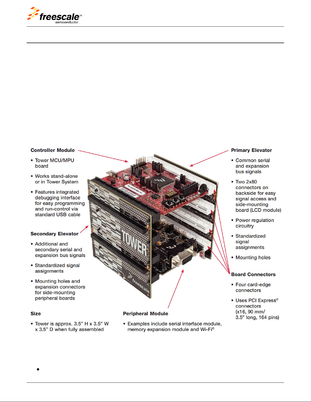
development platforms for a wide variety of applications. Figure 1 provides an overview of the
Freescale Tower System.
Figure 1. Freescale Tower System Overview
1.1 Contents
The TWR-MCF51QM contents include:
TWR-MCF51QM board assembly
TWRMCF51QMUM TWR-MCF51QM Tower Module User's Manual Page 4 of 18

3ft A to mini-B USB cable for debug interface and power
Interactive DVD with software installers and documentation
Quick Start Guide
The TWR-MCF51QM-KIT contains:
TWR-MCF51QM MCU module
TWR-ELEV – Primary and Secondary Elevator Modules
TWR-PROTO – Prototyping module
1.2 Features
Figure 2 shows the TWR-MCF51QM with some of the key features called out. The following list
summarizes the features of the TWR-MCF51QM Tower MCU Module:
Tower compatible microcontroller module
MCF51QM128VLH: MCF51QM with 128 Kbytes of flash in a 64 pin LQFP package
Terminal block for access to high-precision analog IO
Touch Tower Plug-in Socket
General purpose Tower Plug-in (TWRPI) socket
On-board debug circuit (OSBDM) with virtual serial port
Three axis accelerometer (MMA8451Q)
Two (2) user-controllable LEDs
Two (2) capacitive touch pads
One (1) user pushbutton switch
Infrared transmit and receive
Potentiometer
Microphone (ADC) and audio output (DAC)
TWRMCF51QMUM TWR-MCF51QM Tower Module User's Manual Page 5 of 18
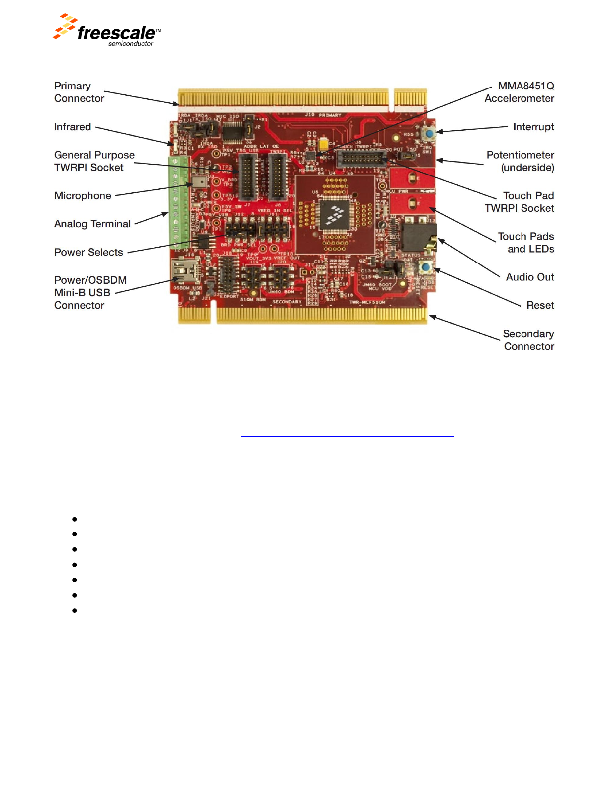
Figure 2. Callouts on front side of the TWR-MCF51QM
1.3 Getting Started
Follow the Quick Start Guide found printed in the TWR-MCF51QM box or the interactive DVD for the
list of recommended steps for getting started. Check for new or revised documentation on the tool
support page for the TWR-MCF51QM: http://www.freescale.com/TWR-MCF51QM.
1.4 Reference Documents
The documents listed below should be referenced for more information on the ColdFire+ devices,
Freescale Tower System, and the TWR-MCF51QM Controller Module. These can be found in the
documentation section of freescale.com/TWR-MCF51QM or freescale.com/coldfire+.
TWR-MCF51QM-QSG: Quick Start Guide
TWR-MCF51QM-SCH: Schematics
TWR-MCF51QM-PWA: Design Package
ColdFire+ Portfolio Product Brief
MCF51QM128 Reference Manual
Tower Configuration Tool
Tower Mechanical Drawing
2 Hardware Description
The TWR-MCF51QM is a Tower Controller Module featuring the MCF51QM128—a ColdFire+ based
microcontroller with high-precision analog in a 64 LQFP package. It is intended for use in the Freescale
Tower System but can operate stand-alone. An on-board debug circuit, OSBDM, provides a BDM
interface and a power supply input through a single USB mini-AB connector. Figure 3 shows a block
diagram of the TWR-MCF51QM. The following sections describe the hardware in more detail.
TWRMCF51QMUM TWR-MCF51QM Tower Module User's Manual Page 6 of 18

Cap Touch
Pads
OSBDM
BDM, Power, SCI
MCF51JF128
64-pin LQFP
Tower Elevator Expansion Connectors
I2S, SPI, I2C, ADC, USB, DAC, PWM, SCI/UART, Flexbus
SCI
Freescale Device
External Connectors Interface Circuits Power
MMA8451Q
Infrared Port
IR Output
I
2
C
Comparator
GPIO / Interrupts
ADC
Reset
LED
BDM
8 MHz XTAL
3.3V5.0V
General Purpose
Tower Plug-in
(TWRPI)
SPI, I2C, ADC, GPIO
Touch Tower Plug-in
(TWRPI)
TSI, GPIO
LED
Microphone
& DAC Output
ADC, DAC
USB
Mini-B
5.0V
TSI
Terminal
Block
Analog Signals
Figure 3. TWR-MCF51QM Block Diagram
2.1 MCF51QM Microcontroller
The TWR-MCF51QM module features the MCF51QM128VLH. The key features of the microcontroller
are listed here:
32-bit ColdFire+ core with FlexMemory, EMAC, and DIV hardware acceleration
50 MHz maximum core operating frequency
64-pin LQFP, 9mm x 9mm
1.71V – 3.6V operating voltage input range
128 Kbytes of program flash, 32 Kbytes of static RAM
FlexMemory consisting of 32 Kbytes of FlexMemory that can be used as additional non-volatile
flash or up to 2KB of enhanced EEPROM.
10 flexible low power modes, ideal for extending battery life
Cryptographic Acceleration Unit (CAU) and Random Number Generator (RNGB)
for secure communications
Integrated capacitive touch sensing support: low power touch sensing interface (TSI)
Integrated 16-bit SAR ADC with up to 18 single-ended channels and one differential pair
Real-time debug support, with six hardware breakpoints that can be configured to halt the
processor or generate debug interrupt
External bus interface
Multi-purpose clock generator with PLL and FLL operation modes; multiple input oscillator or
resonator frequency ranges; two internal trimmable references
TWRMCF51QMUM TWR-MCF51QM Tower Module User's Manual Page 7 of 18

High-speed analog comparator with 6-bit DAC
Programmable voltage reference
SPI, I
GPIO with pin interrupt support, DMA request capability, digital glitch filtering
2
C (w/ SMBUS support), UART (w/ ISO7816 and IrDA),
2.2 Clocking
The ColdFire+ MCUs start up from an internal digitally controlled oscillator (DCO). Software can enable
the main external oscillator (EXTAL2/XTAL2) if desired. The external oscillator/resonator for the
Multipurpose Clock Generator (MCG) module can range from 32.768 KHz up to a 32 MHz.
The TWR-MCF51QM provides an 8 MHz ceramic resonator as shown in Figure 4 below and sheet 4 of
the schematics.
Figure 4. Main Oscillator Input
Additionally, the TWR-MCF51QM provides an optional crystal that can feed the low-power oscillator
(EXTAL1/XTAL1). The low-power oscillator can be used to clock the low-power timer and other
features of the MCF51QM in very low-power stop modes. Two 0 ohm resistors (not populated be
default) provide a means for isolating EXTAL1 and XTAL1 connections to the crystal circuit so that these
pins can be used for other purposes.
Figure 5. Low-power Oscillator Input
2.3 System Power
When installed into a Tower System, the TWR-MCF51QM can be powered from either an on-board
source or from another source in the assembled Tower System.
In stand-alone operation, the main power source for the TWR-MCF51QM module is derived from the
5.0V input from either the OSBDM USB mini-B connector (J16) or the EzPort header (J18) when a shunt
is placed on jumper J24. Two low-dropout regulators provide 3.3V and 1.8V supplies from the 5.0V
input voltage. Additionally, the 3.3V regulator built into the MCF51QM can be selected. All the user
selectable options can be configured using two headers, J11 and J12.
TWRMCF51QMUM TWR-MCF51QM Tower Module User's Manual Page 8 of 18

J13 Shunt Setting
Description
1
2
7
8
1-2
Power from the OSBDM interface (J16) supplied to the onboard voltage regulators. This is a default setting.
1
2
7
8
6-8
Power from the Tower Primary Connector USB device
interface supplied to the MCF51QM on-chip regulator.
J14 Shunt Setting
Description
1
2
7
8
3-5
Board power is supplied by the 3.3V on-board (external)
regulator. This is the default setting.
1
2
7
8
5-7
Board power is supplied by the 1.8V on-board (external)
regulator.
1
2
7
8
1-2
Board power is supplied by the 3.3V MCF51QM on-chip
(internal) regulator.
1
2
7
8
1-3
5-7
Power from the 3.3V MCF51QM on-chip (internal) regulator is
supplied to the 1.8V on-board (external) regulator. Board
power is supplied by the 1.8V on-board (external) regulator.
Note: Take care not to install a shunt on J11 pins 1-2 when
J12 is in this configuration. It is recommended to remove the
shunt from J11 1-2 and use it on J12 for this setting.
1
2
7
8
+
―
―
An external battery or other alternate source can be
connected to pins 5 (positive) and 6 (negative, ground).
The J11 header is used to select the power source that is supplied to one of the three possible voltage
regulators. The J12 header is used to select the regulated board power source. Refer to Table 1 and
Table 2 for details.
Table 1. J11, Regulator Power Source Selection
Table 2. J12, Board Power Source Selection
The 3.3V or 1.8V power supplied to the MCU is routed through a jumper, J15. The jumper shunt can be
removed to allow for either 1) alternate MCU supply voltages to be injected or 2) the measurement of
power consumed by the MCU.
TWRMCF51QMUM TWR-MCF51QM Tower Module User's Manual Page 9 of 18

2.4 Debug Interface
There are two debug interface options provided: the on-board OSBMD circuit and an external
Background Debug Mode (BDM) connector. The BDM connector is a standard 6-pin connector
providing an external debugger cable with access to the BDM interface of the MCF51QM128.
Alternatively, the on-board OSBDM debug interface can be used to access the debug interface of the
MCF51QM128.
2.4.1 OSBDM
An on-board MC9S08JM60 based Open Source BDM (OSBDM) circuit provides a BDM debug interface
to the MCF51QM. A standard USB A male to mini-B male cable (provided) can be used for debugging
via the USB connector, J16. The OSJTAG interface also provides a USB to serial bridge. Drivers for the
OSBDM interface are provided in the P&E Micro OSBDM/OSJTAG Tower Toolkit (available on the
included DVD). These drivers and more utilities can be found online at
http://www.pemicro.com/osbdm.
2.5 Infrared Port
An infrared transmit and receive interface is implemented as shown in Figure 6 below. The CMT_IRO
pin directly drives an infrared diode. The receiver uses an infrared phototransistor connected to an onchip analog comparator through a low-pass filter. Internal to the MCF51QM device, the output of the
analog comparator can be routed to a UART module for easier processing of the incoming data stream.
Figure 6. Infrared Port Implementation
Note: The PTC5 pin is shared between the Infrared circuit and the green LED (D50). Jumper J1 routes
the signal to either the infrared (shunt on pin 2-3) or LED (shunt on 1-2).
TWRMCF51QMUM TWR-MCF51QM Tower Module User's Manual Page 10 of 18

2.6 Accelerometer
An MMA8451Q digital accelerometer is connected to the MCF51QM MCU through an I2C interface
(I2C0, PTC6 and PTC7) and two GPIO/IRQ signals (PTD0 and PTD1).
Figure 7. Accelerometer Circuit
2.7 Potentiometer, Pushbuttons, LEDs
The TWR-MCF51QM features one pushbutton switch (SW1) connected to the IRQ signal (PTB0), one
pushbutton switch (SW2) connected to the master reset signal (PTC1), two capacitive touch pad
electrodes connected to TSI0_CH10 (PTB1) and TSI0_CH9 (PTE1), two user-controllable LEDs—one
green and one orange—connected to GPIO signals (PTC5 and PTA0), and a potentiometer connected to
an ADC input signal (ADC0_SE12, PTD5). Refer to Table 4 “I/O Connectors and Pin Usage Table” for
more information.
2.8 Microphone
A microphone circuit is provided allowing for sampling of audio data. A single-ended ADC signal
(ADC0_SE11, PTD4) is used to sample the value on the microphone IC output. A jumper, J4, is provided
to isolate the ADC signal from the microphone so that it can be used for other purposes (refer to Table
4 “I/O Connectors and Pin Usage Table” for more information).
TWRMCF51QMUM TWR-MCF51QM Tower Module User's Manual Page 11 of 18

Figure 8. Microphone circuit
2.9 Audio Output
The 12-bit DAC output signal from the MCF51QM is connected directly to a standard 3.5 mm audio
jack.
Figure 9. Audio output (DAC) circuit
2.10 General Purpose Tower Plug-in (TWRPI) Socket
The TWR-MCF51QM features a socket that can accept a variety of different Tower Plug-in modules
featuring sensors, RF transceivers, and more. The General Purpose TWRPI socket provides access to
I2C, SPI, IRQs, GPIOs, timers, analog conversion signals, TWRPI ID signals, reset, and voltage supplies.
The pinout for the TWRPI Socket is defined in Table 1.
Refer to Table 4 “I/O Connectors and Pin Usage Table” for the specific MCF51QM pin connections to
the General Purpose TWRPI socket.
TWRMCF51QMUM TWR-MCF51QM Tower Module User's Manual Page 12 of 18

Left-side 2x10 Connector
Right-side 2x10 Connector
Pin
Description
1
5V VCC
2
3.3 V VCC
3
GND
4
3.3V VDDA
5
VSS (Analog GND)
6
VSS (Analog GND)
7
VSS (Analog GND)
8
ADC: Analog 0
9
ADC: Analog 1
10
VSS (Analog GND)
11
VSS (Analog GND)
12
ADC: Analog 2
13
VSS (Analog GND)
14
VSS (Analog GND)
15
GND
16
GND
17
ADC: TWRPI ID 0
18
ADC: TWRPI ID 1
19
GND
20
Reset
Pin
Description
1
GND
2
GND
3
I2C: SCL
4
I2C: SDA
5
GND
6
GND
7
GND
8
GND
9
SPI: MISO
10
SPI: MOSI
11
SPI: SS
12
SPI: CLK
13
GND
14
GND
15
GPIO: GPIO0/IRQ
16
GPIO: GPIO1/IRQ
17
GPIO: GPIO2
18
GPIO: GPIO3
19
GPIO: GPIO4/Timer
20
GPIO: GPIO5/Timer
Pin
Description
1
5V VCC
2
3.3 V VCC
3
Electrode 0
4
3.3V VDDA
5
Electrode 1
6
VSS (Analog GND)
7
Electrode 2
Table 1. General Purpose TWRPI socket pinout
2.11 Touch Interface
The touch sensing input (TSI) module of the ColdFire+ MCUs provides capacitive touch sensing
detection with high sensitivity and enhanced robustness. Each TSI pin implements the capacitive
measurement of an electrode.
The TWR-MCF51QM provides two methods for evaluating the TSI module. There are two electrodes
on-board the TWR-MCF51QM that simulate pushbuttons. Additionally, six TSI signals are connected to
a Touch Tower Plug-in (TWRPI) socket that can accept Touch TWRPI daughter cards that may feature
keypads, rotary dials, sliders, etc.
The pinout for the Touch TWRPI socket is defined in Table 2. Refer to Table 4 “I/O Connectors and Pin
Usage Table” for the specific MCF51QM pin connections to the Touch TWRPI socket.
Table 2. Touch TWRPI socket pinout
TWRMCF51QMUM TWR-MCF51QM Tower Module User's Manual Page 13 of 18

Pin
Description
8
Electrode 3
9
Electrode 4
10
Electrode 5
11
Electrode 6
12
Electrode 7
13
Electrode 8
14
Electrode 9
15
Electrode 10
16
Electrode 11
17
ADC: TWRPI ID 0
18
ADC: TWRPI ID 1
19
GND
20
Reset
2.12 Analog Terminal Block
The MCF51QM features high-precision integrated analog. Many of the external signals are brought to
strip of screw terminals for easy user access.
2.13 External Bus Interface – FlexBus
The MCF51QM device features a multi-function external bus interface called the FlexBus interface
controller capable of interfacing to slave-only devices. The FlexBus interface is not used directly on the
TWR-MCF51QM. Instead, a subset of the FlexBus is connected to the Primary Connector so that the
external bus can access devices on Tower peripheral modules. Refer to Table 5 “TWR-MCF51QM
Primary Connector Pinout” and sheet 9 of the TWR-MCF51QM schematics for more details.
3 Jumper Table
There are several jumpers on the TWR-MCF51QM that provide configuration selection and signal
isolation. Refer to the following table for details. The default installed jumper settings are shown in
bold with asterisks.
TWRMCF51QMUM TWR-MCF51QM Tower Module User's Manual Page 14 of 18
Figure 10. Analog Terminal Block

Jumper
Option
Setting
Description
J1
Infrared Transmitter and
Green LED Connection
*1-2*
Connect PTC5/CMT_IRO to IR Transmitter (D1)
2-3
Connect PTC5 to Green user-controllable LED
J2
Flexbus Address Latch
Selection
1-2
Flexbus address latch disabled
*2-3*
Flexbus address latch enabled
J3
Infrared Received
Connection
ON
Connect PTC2/CMP0_IN3 to IR Receiver (Q1)
*OFF*
Disconnect PTC2/CMP0_IN3 from IR Receiver
J4
Microphone Connection
*ON*
Connect PTD4/ADC0_SE11 to microphone
OFF
Disconnect PTD4/ADC0_SE11 from microphone
J5
Potentiometer
Connection
*ON*
Connect PTD5/ADC0_SE12 to potentiometer
OFF
Disconnect PTD5/ADC0_SE12 from potentiometer
J11
Regulator Power Source
Selection
*1-2*
Refer to Table 1
J12
Board Power Source
Selection
*3-5*
Refer to Table 2
J14
OSBDM Mode Selection
ON
OSBDM bootloader mode (OSBDM firmware reprogramming)
*OFF*
Debugger mode
J15
MCU Power Connection
*ON*
Connect on-board power supply to MCU
OFF
Isolate MCU from power supply (allows for external supply or power
measurements)
J21
EzPort Power Connection
ON
Connect on-board 5V supply to EzPort header (supports powering
board from external EzPort probe)
*OFF*
Disconnect on-board 5V supply from EzPort header
Feature
Connection
Port
Pin
Pin Function
Shared With
OSBDM Virtual
Serial
OSBDM Bridge RX Data
PTD6
UART0_RX
OSBDM Bridge TX Data
PTA7
UART0_TX
Infrared Port
IR Transmit
PTC5
CMT_IRO
LED, GP TWRPI
IR Receive
PTC2
CMP0_IN3
Pushbuttons
SW1 (IRQ)
PTB0
IRQ SW2 (RESET)
PTC1
RESET_B
Touch Pads
E1 / Touch
PTE1
TSI0_CH9
Touch TWRPI
Table 3. TWR-MCF51QM Jumper Table
4 Input/Output Connectors and Pin Usage Table
The following table provides details on which MCF51QM pins are using to communicate with the LEDs,
switches, and other I/O interfaces onboard the TWR-MCF51QM.
Note: Some port pins are used in multiple interfaces on-board and many are potentially connected to
off-board resources via the Tower Primary Connector. Take care to avoid attempted simultaneous
usage of mutually exclusive features.
Table 4. I/O Connectors and Pin Usage Table
TWRMCF51QMUM TWR-MCF51QM Tower Module User's Manual Page 15 of 18

E2 / Touch
PTB1
TSI0_CH10
Touch TWRPI
LEDs
E1 / Orange LED
PTA0
PTA0 /
FTM1_CH0
E2 / Green LED
PTC5
PTC5 / RGPIO5
IR, GP TWRPI
Potentiometer
Potentiometer (R57)
PTD5
ADC0_SE12
GP TWRPI
Microphone
Microphone (U4)
PTD4
ADC0_SE11
GP TWRPI
Audio Output
3.5mm Jack (J16)
―
DAC0_OUT
Accelerometer
I2C SDA
PTC7
I2C0_SDA
GP TWRPI
I2C SCL
PTC6
I2C0_SCL
GP TWRPI
INT1
PTD0
PTD0 (input)
INT2
PTD1
PTD1 (input)
Touch Pad TWRPI
Socket
Electrode 0 (J6 Pin 3)
PTD2
TSI0_CH1
GP TWRPI
Electrode 1 (J6 Pin 5)
PTE1
TSI0_CH9
Touch Pad
Electrode 2 (J6 Pin 7)
PTB1
TSI0_CH10
Touch Pad
Electrode 3 (J6 Pin 8)
PTE2
TSI0_CH11
Electrode 4 (J6 Pin 9)
PTE3
TSI0_CH12
Electrode 5 (J6 Pin 10)
PTB2
TSI0_CH13
TWRPI ID0 (J6 Pin 17)
PTE4
ADC0_SE19
Flexbus
TWRPI ID1 (J6 Pin 18)
PTE5
ADC0_SE20
Flexbus
TWRPI ID1 (J6 Pin 20)
PTC1
RESET_B
General Purpose
TWRPI Socket
TWRPI AN0 (J7 Pin 8)
PTD5
ADC0_SE12
Potentiometer
TWRPI AN1 (J7 Pin 9)
PTD4
ADC0_SE11
Microphone
TWRPI AN2 (J7 Pin 12)
PTD2
ADC0_SE9
Touch TWRPI
TWRPI ID0 (J7 Pin 17)
PTE6
ADC0_SE21
TWRPI ID1 (J7 Pin 18)
PTE7
ADC0_SE22
TWRPI Reset
PTC1
RESET_B
TWRPI I2C SCL (J8 Pin 3)
PTC6
I2C0_SCL
Accelerometer
TWRPI I2C SDA (J8 Pin 4)
PTC7
I2C0_SDA
Accelerometer
TWRPI SPI MISO (J8 Pin 9)
PTA4
SPI1_MISO
TWRPI SPI MOSI (J8 Pin 10)
PTA5
SPI1_MOSI
TWRPI SPI SS (J8 Pin 11)
PTA2
SPI1_SS
TWRPI SPI CLK (J8 Pin 12)
PTA3
SPI1_SCLK
TWRPI GPIO0 (J8 Pin 15)
PTB7
PTB7
TWRPI GPIO1 (J8 Pin 16)
PTC0
PTC0
TWRPI GPIO2 (J8 Pin 17)
PTC5
PTC5
LED, IR
TWRPI GPIO3 (J8 Pin 18)
PTF4
PTF4
Flexbus
TWRPI GPIO4 (J8 Pin 19)
PTF7
PTF7
5 Tower Elevator Connections
The TWR-MCF51QM features two expansion card-edge connectors that interface to the Primary and
Secondary Elevator boards in a Tower system. The Primary Connector (comprised of sides A and B) is
TWRMCF51QMUM TWR-MCF51QM Tower Module User's Manual Page 16 of 18

Pin #
Side B
Pin #
Side A
Name
Usage
Name
Usage
B1
5V
5.0V Power
A1
5V
5.0V Power
B2
GND
Ground
A2
GND
Ground
B3
3.3V
3.3V Power
A3
3.3V
3.3V Power
B4
ELE_PS_SENSE
Elevator Power Sense
A4
3.3V
3.3V Power
B5
GND
Ground
A5
GND
Ground
B6
GND
Ground
A6
GND
Ground
B7
SDHC_CLK / SPI1_CLK
PTC6
A7
SCL0
PTC6
B8
SDHC_D3 / SPI1_CS1_b
A8
SDA0
PTC7
B9
SDHC_D3 / SPI1_CS0_b
PTF0
A9
GPIO9 / CTS1
PTD7
B10
SDHC_CMD / SPI1_MOSI
PTF3
A10
GPIO8 / SDHC_D2
PTB7
B11
SDHC_D0 / SPI1_MISO
PTF2
A11
GPIO7 / SD_WP_DET
PTC0
B12
ETH_COL
A12
ETH_CRS
B13
ETH_RXER
A13
ETH_MDC
B14
ETH_TXCLK
A14
ETH_MDIO
B15
ETH_TXEN
A15
ETH_RXCLK
B16
ETH_TXER
A16
ETH_RXDV
B17
ETH_TXD3
A17
ETH_RXD3
B18
ETH_TXD2
A18
ETH_RXD2
B19
ETH_TXD1
A19
ETH_RXD1
B20
ETH_TXD0
A20
ETH_RXD0
B21
GPIO1 / RTS1
PTE0
A21
SSI_MCLK
B22
GPIO2 / SDHC_D1
PTE2
A22
SSI_BCLK
B23
GPIO3
A23
SSI_FS
B24
CLKIN0
A24
SSI_RXD
B25
CLKOUT1
A25
SSI_TXD
B26
GND
Ground
A26
GND
Ground
B27
AN7
PTD5
A27
AN3
B28
AN6
PTD4
A28
AN2
B29
AN5
PTA6
A29
AN1
B30
AN4
PTD2
A30
AN0
B31
GND
Ground
A31
GND
Ground
B32
DAC1
A32
DAC0
DAC0_OUT
B33
TMR3
A33
TMR1
B34
TMR2
A34
TMR0
B35
GPIO4
PTF7
A35
GPIO6
B36
3.3V
A36
3.3V
3.3V Power
B37
PWM7
A37
PWM3
PTA3
B38
PWM6
A38
PWM2
PTA2
B39
PWM5
PTA5
A39
PWM1
PTA1
B40
PWM4
PTA4
A40
PWM0
PTA0
B41
CANRX0
A41
RXD0
PTF5
B42
CANTX0
A42
TXD0
PTF6
B43
1WIRE
A43
RXD1
PTD6
utilized by the TWR-MCF51QM while the Secondary Connector (comprised of sides C and D) only
makes connections to the GND pins. Table 5 provides the pinout for the Primary Connector.
Table 5. TWR-MCF51QM Primary Connector Pinout
TWRMCF51QMUM TWR-MCF51QM Tower Module User's Manual Page 17 of 18

Pin #
Side B
Pin #
Side A
Name
Usage
Name
Usage
B44
SPI0_MISO
PTA4
A44
TXD1
PTA7
B45
SPI0_MOSI
PTA5
A45
VSS
VSSA
B46
SPI0_CS0_b
PTA2
A46
VDDA
VDDA
B47
SPI0_CS1_b
A47
VREFA1
VREFH
B48
SPI0_CLK
PTA3
A48
VREFA2
VREFL
B49
GND
Ground
A49
GND
Ground
B50
SCL1
PTD1
A50
GPIO14
B51
SDA1
PTD0
A51
GPIO15
B52
GPIO5 / SD_CARD_DET
PTF4
A52
GPIO16
B53
USB0_DP_PDOWN
A53
GPIO17
B54
USB0_DM_PDOWN
A54
USB0_DM
B55
IRQ_H
PTB0
A55
USB0_DP
B56
IRQ_G
PTB0
A56
USB0_ID
B57
IRQ_F
A57
USB0_VBUS
VREGIN
B58
IRQ_E
A58
TMR7
B59
IRQ_D
A59
TMR6
B60
IRQ_C
A60
TMR5
B61
IRQ_B
PTC4
A61
TMR4
B62
IRQ_A
PTC4
A62
RSTIN_b
PTC1
B63
EBI_ALE / EBI_CS1_b
PTB3
A63
RSTOUT_b
PTC1
B64
EBI_CS0_b
PTB2
A64
CLKOUT0
PTC3
B65
GND
Ground
A65
GND
Ground
B66
EBI_AD15
PTA0
A66
EBI_AD14
PTD1
B67
EBI_AD16
PTA1
A67
EBI_AD13
PTD0
B68
EBI_AD17
PTA6
A68
EBI_AD12
PTC7
B69
EBI_AD18
PTC2
A69
EBI_AD11
PTC6
B70
EBI_AD19
PTF4
A70
EBI_AD10
PTF7
B71
EBI_R/W_b
PTF5
A71
EBI_AD9
PTF6
B72
EBI_OE_b
PTE3
A72
EBI_AD8
PTF3
B73
EBI_D7
PTF2
A73
EBI_AD7
Flexbus A7
B74
EBI_D6
PTF1
A74
EBI_AD6
Flexbus A6
B75
EBI_D5
PTF0
A75
EBI_AD5
Flexbus A5
B76
EBI_D4
PTE7
A76
EBI_AD4
Flexbus A4
B77
EBI_D3
PTE6
A77
EBI_AD3
Flexbus A3
B78
EBI_D2
PTE5
A78
EBI_AD2
Flexbus A2
B79
EBI_D1
PTE4
A79
EBI_AD1
Flexbus A1
B80
EBI_D0
PTD3
A80
EBI_AD0
Flexbus A0
B81
GND
Ground
A81
GND
Ground
B82
3.3V
3.3V Power
A82
3.3V
3.3V Power
TWRMCF51QMUM TWR-MCF51QM Tower Module User's Manual Page 18 of 18
 Loading...