

Freescale Semiconductor MC9S12DT128E, MC9S12DG128E, MC9S12DJ128E, MC9S12DG128, MC9S12DJ128 User Manual
...Page 1

MC9S12DT128
Device User Guide
Covers MC9S12DT128E, MC9S12DG128E,
MC9S12DJ128E, MC9S12DG128, MC9S12DJ128,
MC9S12DB128,MC9S12A128,SC515846,SC515847,
SC515848, SC515849, SC101161DT, SC101161DG,
SC101161DJ, SC102202, SC102203, SC102204,
SC102205
HCS12
Microcontrollers
9S12DT128DGV2/D
V02.16
12 APR 2008
freescale.com
Page 2

Device User Guide — 9S12DT128DGV2/D V02.16
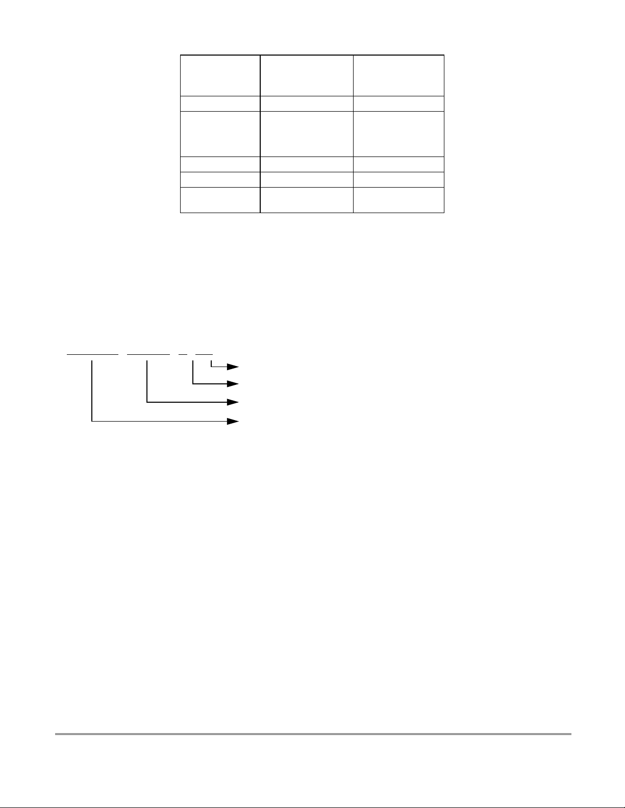
Revision History
Version
Number
V01.00
V01.01
V01.02
V01.03
V01.04
V01.05
V01.06
V02.00
V02.01
Revision
Date
18 Jun
2001
23 July
2001
23 Sep
2001
12 Oct
2001
27 Feb
2002
4 Mar
2002
8 July
2002
11 Jan
2002
01 Feb
2002
Effective
Date
18 June
2001
23 July
2001
23 Sep
2001
12 Oct
2001
27 Feb
2002
4 Mar
2002
22 July
2002
11 Jan
2002
01 Feb
2002
Author Description of Changes
Initial version (parent doc v2.03 dug for dp256).
Updated version after review
Changed Partname, added pierce mode, updated electrical
characteristics
some minor corrections
Replaced Star12 by HCS12
Updated electrical spec after MC-Qualification (IOL/IOH), Data for
Pierce, NVM reliability
New document numbering. Corrected Typos
Increased VDD to 2.35V, removed min. oscillator startup
Removed Document order number except from Cover Sheet
Added:
Pull-up columns to signal table,
example for PLL Filter calculation,
Thermal values for junction to board and package,
BGND pin pull-up
Part Order Information
Global Register Table
Chip Configuration Summary
Modified:
Reduced Wait and Run IDD values
Mode of Operation chapter
changed leakage current for ADC inputs down to +-1uA
Corrected:
Interrupt vector table enable register inconsistencies
PCB layout for 80QFP VREGEN position
NEW MASKSET
Changed part number from DTB128 to DT128
Functional Changes:
ROMCTL changes in Emulation Mode
80 Pin Byteflight package Option available
Flash with 2 Bit Backdoor Key Enable
Additional CAN0 routing to PJ7,6
Improved BDM with sync and acknowledge capabilities
New Part ID number
Improvements:
Significantly improved NVM reliability data
Corrections:
Interrupt vector Table
Updated Block User Guide versions in preface
Updated Appendix A Electrical Characteristics
2
Freescale Semiconductor
Page 3

Device User Guide — 9S12DT128DGV2/D V02.16
Version
Number
V02.02
V02.03
V02.04
V02.05
V02.06
Revision
Date
08 Mar
2002
14 Mar
2002
16 Aug
2002
12 Sep
2002
06 Nov
2002
Effective
Date
08 Mar
2002
14 Mar
2002
16 Aug
2002
12 Sep
2002
06 Nov
2002
Author Description of Changes
Changed XCLKS to PE7 in Table 2-2
Updated device part numbers in Figure 2-1
Updated BDM clock in Figure 3-1
Removed SIM description in overview & n
Updated electrical spec of VDD & VDDPLL (Table A-4), IOL/IOH
(Table A-6), C
Updated interrupt pulse timing variables in Table A-6
Updated device part numbers in Figure 2-1
Added document numbers on cover page and Table 0-2
Cleaned up Fig. 1-1, 2-1
Updated Section 1.5 descriptions
Corrected PE assignment in Table 2-2, Fig. 2-5,6,7.
Corrected NVM sizes in Sections 16, 17
Added I
Added Blank Check in A.3.1.5 and Table A-11
Updated CRG spec in Table A-15
Added:
Pull-up columns to signal table,
Example for PLL Filter calculation,
Thermal values for junction to board and package,
BGND pin pull-up
Part Order Information
Global Register Table
Chip Configuration Summary
Device specific info on CRG
Modified:
Reduced Wait and Run IDD values
Mode of Operation chapter
Changed leakage current for ADC inputs down to +-1uA
Minor modification of PLL frequency/ voltage gain values
Corrected:
Pin names/functions on 80 pin packages
Interrupt vector table enable register inconsistencies
PCB layout for 80QFP VREGEN position
Corrected:
Register address mismatches in 1.5.1
Removed document order no. from Revision History pages
Renamed "Preface" section to "Derivative Differences and
Document references". Added details for derivatives missing
CAN0/1/4, BDLC, IIC and/or Byteflight
Added 2L40K mask set in section 1.6
Added OSC User Guide in Preface, “Document References”
Added oscillator clock connection to BDM in S12_CORE in fig 3-1
Corrected several register and bit names in “Local Enable” column
of Table 5.1 Interrupt Vector Locations
Section HCS12 Core Block Description: mentioned alternate clock
of BDM to be equivalent to oscillator clock
Added new section: “Oscillator (OSC) Block Description”
Corrected in footnote of Table "PLL Characteristics": fOSC = 4MHz
REF
(Table A-9), CIN(Table A-6 & A-15),
INS
spec for 1ATD in Table A-8
UPOSC
spec in TableA-15
Freescale Semiconductor 3
Page 4

Device User Guide — 9S12DT128DGV2/D V02.16
Version
Number
V02.07
V02.08
V02.09
V02.10
V02.11
Revision
Date
29 Jan
2003
26 Feb
2003
15 Oct
2003
6 Feb
2004
3 May
2004
Effective
Date
29 Jan
2003
26 Feb
2003
15 Oct
2003
6 Feb
2004
3 May
2004
Author Description of Changes
Added 3L40K mask set in section 1.6
Corrected register entries in section 1.5.1 “Detailed Memory Map”
Updated description for ROMCTL in section 2.3.31
Updated section 4.3.3 “Unsecuring the Microcontroller”
Corrected and updated device-specific information for OSC
(section 8.1) & Byteflight (section 15.1)
Updated footnote in Table A-4 “Operating Conditions”
Changed reference of VDDM to VDDR in section A.1.8
Removed footnote on input leakage current in Table A-6 “5V I/O
Characteristics”
Added part numbers MC9S12DT128E, MC9S12DG128E, and
MC9S12DJ128E in “Preface” and related part number references
Removed mask sets 0L40K and 2L40K from Table 1-3
Replaced references to HCS12 Core Guide by the individual
HCS12 Block guides in Table 0-2, section 1.5.1, and section 6;
updated Fig.3-1 “Clock Connections” to show the individual HCS12
blocks
Corrected PIM module name and document order number in Table
0-2 “Document References”
Corrected ECT pulse accumulators description in section 1.2
“Features”
Corrected KWP5 pin name in Fig 2-1 112LQFP pin assignments
Corrected pull resistor CTRL/reset states for PE7 and PE4-PE0 in
Table 2.1 “Signal Properties”
Mentioned “S12LRAE” bootloader in Flash section 17
Corrected footnote on clamp of TEST pin under Table A-1
“Absolute Maximum Ratings”
Corrected minimum bus frequency to 0.25MHz in Table A-4
“Operating Conditions”
Replaced “burst programming” by “row programming” in A.3 “NVM,
Flash and EEPROM”
Corrected blank check time for EEPROM in Table A-11 “NVM
Timing Characteristics”
Corrected operating frequency in Table A-18 “SPI Master/Slave
Mode Timing Characteristics
Added A128 information in “Derivative Differences”, 2.1 “Device
Pinout”, 2.2 “Signal Properties Summary”, Fig 23-2 & Fig 23-4
Added lead-free package option (PVE) in Table 0-2 “Derivative
Differences for MC9S12DB128” and Fig 0-1 “Order Partnumber
Example”
Added an “AEC qualified” row in the “Derivative Differences” tables
0-1 & 0-2.
Added part numbers SC515846, SC515847, SC515848, and
SC515849 in “Derivative Differences” tables 0-1 & 0-2, section 2,
and section 23.
Corrected and added maskset 4L40K in tables 0-1 & 0-2 and
section 1.6.
Corrected BDLC module availability in DB128 80QFP part in
“Derivative Differences” table 0-2.
4
Freescale Semiconductor
Page 5

Device User Guide — 9S12DT128DGV2/D V02.16
Version
Number
V02.12
V02.13
V02.14
V02.15
V02.16
Revision
Date
06 Dec
2004
04 Mar
2005
28 Apr
2005
05 Oct
2005
12 Apr
2008
Effective
Date
06 Dec
2004
04 Mar
2005
28 Apr
2005
05 Oct
2005
12 Apr
2008
Author Description of Changes
Added maskset 0L94R
Added items V
IH,EXTAL
“Oscillator characteristics”
Removeditem “Oscillator” from table A-4 “Operating Conditions” as
it is already covered in table “Oscillator Characteristics”
Amended feature list of A128 in Table 0-1 “Derivative Differences”
Updated cover page
Added part numbers SC101161DT, SC101161DG, SC101161DJ,
SC102202, SC102203, SC102204, & SC102205
Added masksets 5L40K &1L59W
Changed T
to 85°C in table A-12 “NVM Reliability” & added
Javg
footnote concerning data retention
Updated “NVM Reliability” table A-12 format with added data.
Added figure A-2 “Typical Endurance vs Temperature”
Added maskset 2L94R
, V
IL,EXTAL
, & V
HYS,EXTAL
in table A-15
Freescale Semiconductor 5
Page 6

Device User Guide — 9S12DT128DGV2/D V02.16
6
Freescale Semiconductor
Page 7

Device User Guide — 9S12DT128DGV2/D V02.16
Table of Contents
Section 1 Introduction
1.1 Overview. . . . . . . . . . . . . . . . . . . . . . . . . . . . . . . . . . . . . . . . . . . . . . . . . . . . . . . . . . 25
1.2 Features . . . . . . . . . . . . . . . . . . . . . . . . . . . . . . . . . . . . . . . . . . . . . . . . . . . . . . . . . . 25
1.3 Modes of Operation . . . . . . . . . . . . . . . . . . . . . . . . . . . . . . . . . . . . . . . . . . . . . . . . .27
1.4 Block Diagram . . . . . . . . . . . . . . . . . . . . . . . . . . . . . . . . . . . . . . . . . . . . . . . . . . . . . 28
1.5 Device Memory Map. . . . . . . . . . . . . . . . . . . . . . . . . . . . . . . . . . . . . . . . . . . . . . . . . 30
1.5.1 Detailed Register Map . . . . . . . . . . . . . . . . . . . . . . . . . . . . . . . . . . . . . . . . . . . . . 32
1.6 Part ID Assignments. . . . . . . . . . . . . . . . . . . . . . . . . . . . . . . . . . . . . . . . . . . . . . . . . 55
Section 2 Signal Description
2.1 Device Pinout . . . . . . . . . . . . . . . . . . . . . . . . . . . . . . . . . . . . . . . . . . . . . . . . . . . . . . 57
2.2 Signal Properties Summary . . . . . . . . . . . . . . . . . . . . . . . . . . . . . . . . . . . . . . . . . . . 60
2.3 Detailed Signal Descriptions. . . . . . . . . . . . . . . . . . . . . . . . . . . . . . . . . . . . . . . . . . . 64
2.3.1 EXTAL, XTAL — Oscillator Pins . . . . . . . . . . . . . . . . . . . . . . . . . . . . . . . . . . . . . 64
2.3.2 RESET — External Reset Pin . . . . . . . . . . . . . . . . . . . . . . . . . . . . . . . . . . . . . . . 64
2.3.3 TEST — Test Pin. . . . . . . . . . . . . . . . . . . . . . . . . . . . . . . . . . . . . . . . . . . . . . . . . 64
2.3.4 XFC — PLL Loop Filter Pin . . . . . . . . . . . . . . . . . . . . . . . . . . . . . . . . . . . . . . . . . 64
2.3.5 BKGD / TAGHI / MODC — Background Debug, Tag High, and Mode Pin . . . . . 64
2.3.6 PAD[15] / AN1[7] / ETRIG1 — Port AD Input Pin [15] . . . . . . . . . . . . . . . . . . . . . 65
2.3.7 PAD[14:8] / AN1[6:0] — Port AD Input Pins [14:8]. . . . . . . . . . . . . . . . . . . . . . . . 65
2.3.8 PAD[7] / AN0[7] / ETRIG0 — Port AD Input Pin [7] . . . . . . . . . . . . . . . . . . . . . . . 65
2.3.9 PAD[6:0] / AN0[6:0] — Port AD Input Pins [6:0]. . . . . . . . . . . . . . . . . . . . . . . . . . 65
2.3.10 PA[7:0] / ADDR[15:8] / DATA[15:8] — Port A I/O Pins . . . . . . . . . . . . . . . . . . . . 65
2.3.11 PB[7:0] / ADDR[7:0] / DATA[7:0] — Port B I/O Pins . . . . . . . . . . . . . . . . . . . . . . 65
2.3.12 PE7 / NOACC / XCLKS — Port E I/O Pin 7. . . . . . . . . . . . . . . . . . . . . . . . . . . . . 65
2.3.13 PE6 / MODB / IPIPE1 — Port E I/O Pin 6 . . . . . . . . . . . . . . . . . . . . . . . . . . . . . . 67
2.3.14 PE5 / MODA / IPIPE0 — Port E I/O Pin 5 . . . . . . . . . . . . . . . . . . . . . . . . . . . . . . 67
2.3.15 PE4 / ECLK — Port E I/O Pin 4 . . . . . . . . . . . . . . . . . . . . . . . . . . . . . . . . . . . . . . 67
2.3.16 PE3 / LSTRB / TAGLO — Port E I/O Pin 3 . . . . . . . . . . . . . . . . . . . . . . . . . . . . . 67
2.3.17 PE2 / R/W — Port E I/O Pin 2 . . . . . . . . . . . . . . . . . . . . . . . . . . . . . . . . . . . . . . . 67
2.3.18 PE1 / IRQ — Port E Input Pin 1. . . . . . . . . . . . . . . . . . . . . . . . . . . . . . . . . . . . . . 67
2.3.19 PE0 / XIRQ — Port E Input Pin 0. . . . . . . . . . . . . . . . . . . . . . . . . . . . . . . . . . . . . 67
2.3.20 PH7 / KWH7 — Port H I/O Pin 7 . . . . . . . . . . . . . . . . . . . . . . . . . . . . . . . . . . . . . 67
Freescale Semiconductor
7
Page 8

Device User Guide — 9S12DT128DGV2/D V02.16
2.3.21 PH6 / KWH6 — Port H I/O Pin 6 . . . . . . . . . . . . . . . . . . . . . . . . . . . . . . . . . . . . . 68
2.3.22 PH5 / KWH5 — Port H I/O Pin 5 . . . . . . . . . . . . . . . . . . . . . . . . . . . . . . . . . . . . . 68
2.3.23 PH4 / KWH4 — Port H I/O Pin 2 . . . . . . . . . . . . . . . . . . . . . . . . . . . . . . . . . . . . . 68
2.3.24 PH3 / KWH3 / SS1 — Port H I/O Pin 3 . . . . . . . . . . . . . . . . . . . . . . . . . . . . . . . . 68
2.3.25 PH2 / KWH2 / SCK1 — Port H I/O Pin 2 . . . . . . . . . . . . . . . . . . . . . . . . . . . . . . . 68
2.3.26 PH1 / KWH1 / MOSI1 — Port H I/O Pin 1 . . . . . . . . . . . . . . . . . . . . . . . . . . . . . . 68
2.3.27 PH0 / KWH0 / MISO1 — Port H I/O Pin 0 . . . . . . . . . . . . . . . . . . . . . . . . . . . . . . 68
2.3.28 PJ7 / KWJ7 / TXCAN4 / SCL / TXCAN0 — PORT J I/O Pin 7. . . . . . . . . . . . . . . 68
2.3.29 PJ6 / KWJ6 / RXCAN4 / SDA / RXCAN0 — PORT J I/O Pin 6 . . . . . . . . . . . . . . 69
2.3.30 PJ[1:0] / KWJ[1:0] — Port J I/O Pins [1:0] . . . . . . . . . . . . . . . . . . . . . . . . . . . . . . 69
2.3.31 PK7 / ECS / ROMCTL — Port K I/O Pin 7. . . . . . . . . . . . . . . . . . . . . . . . . . . . . . 69
2.3.32 PK[5:0] / XADDR[19:14] — Port K I/O Pins [5:0] . . . . . . . . . . . . . . . . . . . . . . . . . 69
2.3.33 PM7 / BF_PSLM / TXCAN4 — Port M I/O Pin 7 . . . . . . . . . . . . . . . . . . . . . . . . . 69
2.3.34 PM6 / BF_PERR / RXCAN4 — Port M I/O Pin 6 . . . . . . . . . . . . . . . . . . . . . . . . . 69
2.3.35 PM5 / BF_PROK / TXCAN0 / TXCAN4 / SCK0 — Port M I/O Pin 5 . . . . . . . . . . 69
2.3.36 PM4 / BF_PSYN / RXCAN0 / RXCAN4/ MOSI0 — Port M I/O Pin 4. . . . . . . . . . 70
2.3.37 PM3 / TX_BF / TXCAN1 / TXCAN0 / SS0 — Port M I/O Pin 3 . . . . . . . . . . . . . . 70
2.3.38 PM2 / RX_BF / RXCAN1 / RXCAN0 / MISO0 — Port M I/O Pin 2. . . . . . . . . . . . 70
2.3.39 PM1 / TXCAN0 / TXB — Port M I/O Pin 1 . . . . . . . . . . . . . . . . . . . . . . . . . . . . . . 70
2.3.40 PM0 / RXCAN0 / RXB — Port M I/O Pin 0. . . . . . . . . . . . . . . . . . . . . . . . . . . . . . 70
2.3.41 PP7 / KWP7 / PWM7 — Port P I/O Pin 7. . . . . . . . . . . . . . . . . . . . . . . . . . . . . . . 70
2.3.42 PP6 / KWP6 / PWM6 — Port P I/O Pin 6. . . . . . . . . . . . . . . . . . . . . . . . . . . . . . . 70
2.3.43 PP5 / KWP5 / PWM5 — Port P I/O Pin 5. . . . . . . . . . . . . . . . . . . . . . . . . . . . . . . 71
2.3.44 PP4 / KWP4 / PWM4 — Port P I/O Pin 4. . . . . . . . . . . . . . . . . . . . . . . . . . . . . . . 71
2.3.45 PP3 / KWP3 / PWM3 / SS1 — Port P I/O Pin 3. . . . . . . . . . . . . . . . . . . . . . . . . . 71
2.3.46 PP2 / KWP2 / PWM2 / SCK1 — Port P I/O Pin 2 . . . . . . . . . . . . . . . . . . . . . . . . 71
2.3.47 PP1 / KWP1 / PWM1 / MOSI1 — Port P I/O Pin 1. . . . . . . . . . . . . . . . . . . . . . . . 71
2.3.48 PP0 / KWP0 / PWM0 / MISO1 — Port P I/O Pin 0. . . . . . . . . . . . . . . . . . . . . . . . 71
2.3.49 PS7 / SS0 — Port S I/O Pin 7 . . . . . . . . . . . . . . . . . . . . . . . . . . . . . . . . . . . . . . . 71
2.3.50 PS6 / SCK0 — Port S I/O Pin 6 . . . . . . . . . . . . . . . . . . . . . . . . . . . . . . . . . . . . . . 71
2.3.51 PS5 / MOSI0 — Port S I/O Pin 5 . . . . . . . . . . . . . . . . . . . . . . . . . . . . . . . . . . . . . 72
2.3.52 PS4 / MISO0 — Port S I/O Pin 4 . . . . . . . . . . . . . . . . . . . . . . . . . . . . . . . . . . . . . 72
2.3.53 PS3 / TXD1 — Port S I/O Pin 3 . . . . . . . . . . . . . . . . . . . . . . . . . . . . . . . . . . . . . . 72
2.3.54 PS2 / RXD1 — Port S I/O Pin 2. . . . . . . . . . . . . . . . . . . . . . . . . . . . . . . . . . . . . . 72
2.3.55 PS1 / TXD0 — Port S I/O Pin 1 . . . . . . . . . . . . . . . . . . . . . . . . . . . . . . . . . . . . . . 72
2.3.56 PS0 / RXD0 — Port S I/O Pin 0. . . . . . . . . . . . . . . . . . . . . . . . . . . . . . . . . . . . . . 72
8
Freescale Semiconductor
Page 9

Device User Guide — 9S12DT128DGV2/D V02.16
2.3.57 PT[7:0] / IOC[7:0] — Port T I/O Pins [7:0] . . . . . . . . . . . . . . . . . . . . . . . . . . . . . . 72
2.4 Power Supply Pins . . . . . . . . . . . . . . . . . . . . . . . . . . . . . . . . . . . . . . . . . . . . . . . . . . 72
2.4.1 VDDX,VSSX — Power & Ground Pins for I/O Drivers. . . . . . . . . . . . . . . . . . . . . 73
2.4.2 VDDR, VSSR — Power & Ground Pins for I/O Drivers & for Internal Voltage Regulator
. . . . . . . . . . . . . . . . . . . . . . . . . . . . . . . . . . . . . . . . . . . . . . . . . . . . . . . . . . . . . . . 73
2.4.3 VDD1, VDD2, VSS1, VSS2 — Internal Logic Power Supply Pins. . . . . . . . . . . . 73
2.4.4 VDDA, VSSA — Power Supply Pins for ATD and VREG . . . . . . . . . . . . . . . . . . 74
2.4.5 VRH, VRL — ATD Reference Voltage Input Pins . . . . . . . . . . . . . . . . . . . . . . . . 74
2.4.6 VDDPLL, VSSPLL — Power Supply Pins for PLL. . . . . . . . . . . . . . . . . . . . . . . . 74
2.4.7 VREGEN — On Chip Voltage Regulator Enable. . . . . . . . . . . . . . . . . . . . . . . . . 74
Section 3 System Clock Description
3.1 Overview. . . . . . . . . . . . . . . . . . . . . . . . . . . . . . . . . . . . . . . . . . . . . . . . . . . . . . . . . . 75
Section 4 Modes of Operation
4.1 Overview. . . . . . . . . . . . . . . . . . . . . . . . . . . . . . . . . . . . . . . . . . . . . . . . . . . . . . . . . . 77
4.2 Chip Configuration Summary . . . . . . . . . . . . . . . . . . . . . . . . . . . . . . . . . . . . . . . . . . 77
4.3 Security. . . . . . . . . . . . . . . . . . . . . . . . . . . . . . . . . . . . . . . . . . . . . . . . . . . . . . . . . . .78
4.3.1 Securing the Microcontroller . . . . . . . . . . . . . . . . . . . . . . . . . . . . . . . . . . . . . . . . 78
4.3.2 Operation of the Secured Microcontroller . . . . . . . . . . . . . . . . . . . . . . . . . . . . . . 78
4.3.3 Unsecuring the Microcontroller . . . . . . . . . . . . . . . . . . . . . . . . . . . . . . . . . . . . . . 79
4.4 Low Power Modes . . . . . . . . . . . . . . . . . . . . . . . . . . . . . . . . . . . . . . . . . . . . . . . . . . 79
4.4.1 Stop . . . . . . . . . . . . . . . . . . . . . . . . . . . . . . . . . . . . . . . . . . . . . . . . . . . . . . . . . . . 79
4.4.2 Pseudo Stop. . . . . . . . . . . . . . . . . . . . . . . . . . . . . . . . . . . . . . . . . . . . . . . . . . . . . 79
4.4.3 Wait . . . . . . . . . . . . . . . . . . . . . . . . . . . . . . . . . . . . . . . . . . . . . . . . . . . . . . . . . . . 79
4.4.4 Run. . . . . . . . . . . . . . . . . . . . . . . . . . . . . . . . . . . . . . . . . . . . . . . . . . . . . . . . . . . . 79
Section 5 Resets and Interrupts
5.1 Overview. . . . . . . . . . . . . . . . . . . . . . . . . . . . . . . . . . . . . . . . . . . . . . . . . . . . . . . . . . 81
5.2 Vectors . . . . . . . . . . . . . . . . . . . . . . . . . . . . . . . . . . . . . . . . . . . . . . . . . . . . . . . . . . . 81
5.2.1 Vector Table. . . . . . . . . . . . . . . . . . . . . . . . . . . . . . . . . . . . . . . . . . . . . . . . . . . . . 81
5.3 Effects of Reset . . . . . . . . . . . . . . . . . . . . . . . . . . . . . . . . . . . . . . . . . . . . . . . . . . . . 82
5.3.1 I/O pins. . . . . . . . . . . . . . . . . . . . . . . . . . . . . . . . . . . . . . . . . . . . . . . . . . . . . . . . . 82
5.3.2 Memory . . . . . . . . . . . . . . . . . . . . . . . . . . . . . . . . . . . . . . . . . . . . . . . . . . . . . . . . 83
Section 6 HCS12 Core Block Description
6.1 CPU Block Description. . . . . . . . . . . . . . . . . . . . . . . . . . . . . . . . . . . . . . . . . . . . . . . 85
Freescale Semiconductor
9
Page 10

Device User Guide — 9S12DT128DGV2/D V02.16
6.1.1 Device-specific information . . . . . . . . . . . . . . . . . . . . . . . . . . . . . . . . . . . . . . . . . 85
6.2 HCS12 Module Mapping Control (MMC) Block Description. . . . . . . . . . . . . . . . . . .85
6.2.1 Device-specific information . . . . . . . . . . . . . . . . . . . . . . . . . . . . . . . . . . . . . . . . . 85
6.3 HCS12 Multiplexed External Bus Interface (MEBI) Block Description . . . . . . . . . . . 85
6.3.1 Device-specific information . . . . . . . . . . . . . . . . . . . . . . . . . . . . . . . . . . . . . . . . . 85
6.4 HCS12 Interrupt (INT) Block Description . . . . . . . . . . . . . . . . . . . . . . . . . . . . . . . . . 86
6.5 HCS12 Background Debug Module (BDM) Block Description. . . . . . . . . . . . . . . . . 86
6.5.1 Device-specific information . . . . . . . . . . . . . . . . . . . . . . . . . . . . . . . . . . . . . . . . . 86
6.6 HCS12 Breakpoint (BKP) Block Description . . . . . . . . . . . . . . . . . . . . . . . . . . . . . . 86
Section 7 Clock and Reset Generator (CRG) Block Description
7.1 Device-specific information. . . . . . . . . . . . . . . . . . . . . . . . . . . . . . . . . . . . . . . . . . . . 86
Section 8 Oscillator (OSC) Block Description
8.1 Device-specific information. . . . . . . . . . . . . . . . . . . . . . . . . . . . . . . . . . . . . . . . . . . . 86
Section 9 Enhanced Capture Timer (ECT) Block Description
Section 10 Analog to Digital Converter (ATD) Block Description
Section 11 Inter-IC Bus (IIC) Block Description
Section 12 Serial Communications Interface (SCI) Block Description
Section 13 Serial Peripheral Interface (SPI) Block Description
Section 14 J1850 (BDLC) Block Description
Section 15 Byteflight (BF) Block Description
15.1 Device-specific information. . . . . . . . . . . . . . . . . . . . . . . . . . . . . . . . . . . . . . . . . . . . 88
Section 16 Pulse Width Modulator (PWM) Block Description
Section 17 Flash EEPROM 128K Block Description
Section 18 EEPROM 2K Block Description
Section 19 RAM Block Description
10
Freescale Semiconductor
Page 11

Device User Guide — 9S12DT128DGV2/D V02.16
Section 20 MSCAN Block Description
Section 21 Port Integration Module (PIM) Block Description
Section 22 Voltage Regulator (VREG) Block Description
Section 23 Printed Circuit Board Layout Proposal
Appendix A Electrical Characteristics
A.1 General. . . . . . . . . . . . . . . . . . . . . . . . . . . . . . . . . . . . . . . . . . . . . . . . . . . . . . . . . . . 97
A.1.1 Parameter Classification . . . . . . . . . . . . . . . . . . . . . . . . . . . . . . . . . . . . . . . . . . . 97
A.1.2 Power Supply. . . . . . . . . . . . . . . . . . . . . . . . . . . . . . . . . . . . . . . . . . . . . . . . . . . . 97
A.1.3 Pins . . . . . . . . . . . . . . . . . . . . . . . . . . . . . . . . . . . . . . . . . . . . . . . . . . . . . . . . . . . 98
A.1.4 Current Injection. . . . . . . . . . . . . . . . . . . . . . . . . . . . . . . . . . . . . . . . . . . . . . . . . . 98
A.1.5 Absolute Maximum Ratings . . . . . . . . . . . . . . . . . . . . . . . . . . . . . . . . . . . . . . . . . 99
A.1.6 ESD Protection and Latch-up Immunity. . . . . . . . . . . . . . . . . . . . . . . . . . . . . . . . 99
A.1.7 Operating Conditions . . . . . . . . . . . . . . . . . . . . . . . . . . . . . . . . . . . . . . . . . . . . . 100
A.1.8 Power Dissipation and Thermal Characteristics . . . . . . . . . . . . . . . . . . . . . . . . 101
A.1.9 I/O Characteristics . . . . . . . . . . . . . . . . . . . . . . . . . . . . . . . . . . . . . . . . . . . . . . . 103
A.1.10 Supply Currents . . . . . . . . . . . . . . . . . . . . . . . . . . . . . . . . . . . . . . . . . . . . . . . . . 104
A.2 ATD Characteristics . . . . . . . . . . . . . . . . . . . . . . . . . . . . . . . . . . . . . . . . . . . . . . . . 107
A.2.1 ATD Operating Characteristics . . . . . . . . . . . . . . . . . . . . . . . . . . . . . . . . . . . . . 107
A.2.2 Factors influencing accuracy . . . . . . . . . . . . . . . . . . . . . . . . . . . . . . . . . . . . . . . 107
A.2.3 ATD accuracy. . . . . . . . . . . . . . . . . . . . . . . . . . . . . . . . . . . . . . . . . . . . . . . . . . . 109
A.3 NVM, Flash and EEPROM. . . . . . . . . . . . . . . . . . . . . . . . . . . . . . . . . . . . . . . . . . . 111
A.3.1 NVM timing. . . . . . . . . . . . . . . . . . . . . . . . . . . . . . . . . . . . . . . . . . . . . . . . . . . . . 111
A.3.2 NVM Reliability. . . . . . . . . . . . . . . . . . . . . . . . . . . . . . . . . . . . . . . . . . . . . . . . . . 113
A.4 Voltage Regulator. . . . . . . . . . . . . . . . . . . . . . . . . . . . . . . . . . . . . . . . . . . . . . . . . . 117
A.5 Reset, Oscillator and PLL. . . . . . . . . . . . . . . . . . . . . . . . . . . . . . . . . . . . . . . . . . . . 119
A.5.1 Startup . . . . . . . . . . . . . . . . . . . . . . . . . . . . . . . . . . . . . . . . . . . . . . . . . . . . . . . . 119
A.5.2 Oscillator . . . . . . . . . . . . . . . . . . . . . . . . . . . . . . . . . . . . . . . . . . . . . . . . . . . . . . 120
A.5.3 Phase Locked Loop . . . . . . . . . . . . . . . . . . . . . . . . . . . . . . . . . . . . . . . . . . . . . . 121
A.6 MSCAN. . . . . . . . . . . . . . . . . . . . . . . . . . . . . . . . . . . . . . . . . . . . . . . . . . . . . . . . . . 127
A.7 SPI . . . . . . . . . . . . . . . . . . . . . . . . . . . . . . . . . . . . . . . . . . . . . . . . . . . . . . . . . . . . . 129
A.7.1 Master Mode . . . . . . . . . . . . . . . . . . . . . . . . . . . . . . . . . . . . . . . . . . . . . . . . . . . 129
A.7.2 Slave Mode . . . . . . . . . . . . . . . . . . . . . . . . . . . . . . . . . . . . . . . . . . . . . . . . . . . . 131
Freescale Semiconductor
11
Page 12

Device User Guide — 9S12DT128DGV2/D V02.16
A.8 External Bus Timing . . . . . . . . . . . . . . . . . . . . . . . . . . . . . . . . . . . . . . . . . . . . . . . . 133
A.8.1 General Multiplexed Bus Timing . . . . . . . . . . . . . . . . . . . . . . . . . . . . . . . . . . . . 133
Appendix B Package Information
B.1 General. . . . . . . . . . . . . . . . . . . . . . . . . . . . . . . . . . . . . . . . . . . . . . . . . . . . . . . . . . 137
B.2 112-pin LQFP package. . . . . . . . . . . . . . . . . . . . . . . . . . . . . . . . . . . . . . . . . . . . . . 138
B.3 80-pin QFP package. . . . . . . . . . . . . . . . . . . . . . . . . . . . . . . . . . . . . . . . . . . . . . . . 139
12
Freescale Semiconductor
Page 13

Device User Guide — 9S12DT128DGV2/D V02.16
List of Figures
Figure 0-1 Order Partnumber Example. . . . . . . . . . . . . . . . . . . . . . . . . . . . . . . . . . . . . . 20
Figure 1-1 MC9S12DT128 Block Diagram . . . . . . . . . . . . . . . . . . . . . . . . . . . . . . . . . . . 29
Figure 1-2 MC9S12DT128 Memory Map . . . . . . . . . . . . . . . . . . . . . . . . . . . . . . . . . . . . 31
Figure 2-1 Pin assignments 112 LQFP for MC9S12DT128E, MC9S12DT128,
MC9S12DG128E, MC9S12DG128, MC9S12DJ128E, MC9S12DJ128, MC9S12DB128
MC9S12A128, SC515846, SC515847, SC515848, SC515849, SC101161DT, SC101161DG,
SC101161DJ, SC102202, SC102203, SC102204, and SC102205 . . . . . . . . . . . . . . . . . . 58
Figure 2-2 Pin Assignments in 80 QFP for MC9S12DG128E, MC9S12DG128,
MC9S12DJ128E, MC9S12DJ128, MC9S12A128, SC515847, SC515848, SC101161DG,
SC101161DJ, SC102203, and SC102204 Bondout . . . . . . . . . . . . . . . . . . . . . . . . . . . . . . 59
Figure 2-3 Pin Assignments in 80 QFP for MC9S12DB128, SC515846, and SC102202 Bond-
out . . . . . . . . . . . . . . . . . . . . . . . . . . . . . . . . . . . . . . . . . . . . . . . . . . . . . . . . . . . . 60
Figure 2-4 PLL Loop Filter Connections . . . . . . . . . . . . . . . . . . . . . . . . . . . . . . . . . . . . . 64
Figure 2-5 Colpitts Oscillator Connections (PE7=1) . . . . . . . . . . . . . . . . . . . . . . . . . . . . 66
Figure 2-6 Pierce Oscillator Connections (PE7=0) . . . . . . . . . . . . . . . . . . . . . . . . . . . . . 66
Figure 2-7 External Clock Connections (PE7=0) . . . . . . . . . . . . . . . . . . . . . . . . . . . . . . 66
Figure 3-1 Clock Connections. . . . . . . . . . . . . . . . . . . . . . . . . . . . . . . . . . . . . . . . . . . . . 75
Figure 23-1 Recommended PCB Layout for 112LQFP Colpitts Oscillator . . . . . . . . . . . . 91
Figure 23-2 Recommended PCB Layout for 80QFP (MC9S12DG128E, MC9S12DG128,
MC9S12DJ128E, MC9S12DJ128, MC9S12A128, SC515847, SC515848, SC101161DG,
SC101161DJ, SC102203, and SC102204) Colpitts Oscillator . . . . . . . . . . . . . . . . . . . . . . 92
Figure 23-3 Recommended PCB Layout for 112LQFP Pierce Oscillator . . . . . . . . . . . . . 93
Figure 23-4 Recommended PCB Layout for 80QFP (MC9S12DG128E, MC9S12DG128,
MC9S12DJ128E, MC9S12DJ128, MC9S12A128, SC515847, SC515848, SC101161DG,
SC101161DJ, SC102203, and SC102204) Pierce Oscillator . . . . . . . . . . . . . . . . . . . . . . . 94
Figure 23-5 Recommended PCB Layout for 80QFP (MC9S12DB128, SC515846, and
SC102202) Pierce Oscillator. . . . . . . . . . . . . . . . . . . . . . . . . . . . . . . . . . . . . . . . . . . . . . . . 95
Figure A-1 ATD Accuracy Definitions . . . . . . . . . . . . . . . . . . . . . . . . . . . . . . . . . . . . . 110
Figure A-2 Typical Endurance vs Temperature. . . . . . . . . . . . . . . . . . . . . . . . . . . . . . 115
Figure A-3 Basic PLL functional diagram . . . . . . . . . . . . . . . . . . . . . . . . . . . . . . . . . . 122
Figure A-4 Jitter Definitions. . . . . . . . . . . . . . . . . . . . . . . . . . . . . . . . . . . . . . . . . . . . . 124
Figure A-5 Maximum bus clock jitter approximation . . . . . . . . . . . . . . . . . . . . . . . . . . 124
Figure A-6 SPI Master Timing (CPHA = 0) . . . . . . . . . . . . . . . . . . . . . . . . . . . . . . . . . 129
Figure A-7 SPI Master Timing (CPHA =1). . . . . . . . . . . . . . . . . . . . . . . . . . . . . . . . . . 130
Figure A-8 SPI Slave Timing (CPHA = 0) . . . . . . . . . . . . . . . . . . . . . . . . . . . . . . . . . . 131
Figure A-9 SPI Slave Timing (CPHA =1). . . . . . . . . . . . . . . . . . . . . . . . . . . . . . . . . . . 131
Freescale Semiconductor
13
Page 14

Device User Guide — 9S12DT128DGV2/D V02.16
Figure A-10 General External Bus Timing. . . . . . . . . . . . . . . . . . . . . . . . . . . . . . . . . . . 134
Figure 23-6 112-pin LQFP mechanical dimensions (case no. 987) . . . . . . . . . . . . . . . .138
14
Freescale Semiconductor
Page 15

Device User Guide — 9S12DT128DGV2/D V02.16
List of Tables
Table 0-1 Derivative Differences1 . . . . . . . . . . . . . . . . . . . . . . . . . . . . . . . . . . . . . . . . . . 19
Table 0-2 Derivative Differences for MC9S12DB1281. . . . . . . . . . . . . . . . . . . . . . . . . . . 19
Table 0-3 Document References. . . . . . . . . . . . . . . . . . . . . . . . . . . . . . . . . . . . . . . . . . . 23
Table 1-1 Device Memory Map . . . . . . . . . . . . . . . . . . . . . . . . . . . . . . . . . . . . . . . . . . . . 30
$0000 - $000FMEBI map 1 of 3 (HCS12 Multiplexed External Bus Interface) ................... 32
$0010 - $0014 MMC map 1 of 4 (HCS12 Module Mapping Control) ................................. 32
$0015 - $0016 INT map 1 of 2 (HCS12 Interrupt) .............................................................. 33
$0017 - $0017MMC map 2 of 4 (HCS12 Module Mapping Control) .................................. 33
$0018 - $0019Reserved ..................................................................................................... 33
$001A - $001B Device ID Register ((Table 1-3)) ............................................................... 33
$001C - $001D MMC map 3 of 4 (HCS12 Module Mapping Control, (Table 1-4)) ............ 33
$001E - $001EMEBI map 2 of 3 (HCS12 Multiplexed External Bus Interface) ..................33
$001F - $001FINT map 2 of 2 (HCS12 Interrupt) ............................................................... 34
$0020 - $0027 Reserved .................................................................................................... 34
$0028 - $002F BKP (HCS12 Breakpoint) ........................................................................... 34
$0030 - $0031 MMC map 4 of 4 (HCS12 Module Mapping Control) ................................. 34
$0032 - $0033 MEBI map 3 of 3 (HCS12 Multiplexed External Bus Interface) .................. 34
$0034 - $003F CRG (Clock and Reset Generator) ............................................................ 35
$0040 - $007F ECT (Enhanced Capture Timer 16 Bit 8 Channels) ................................... 35
$0080 - $009F ATD0 (Analog to Digital Converter 10 Bit 8 Channel) ................................ 38
$00A0 - $00C7 PWM (Pulse Width Modulator 8 Bit 8 Channel) ........................................ 39
$00C8 - $00CF SCI0 (Asynchronous Serial Interface) ...................................................... 41
$00D0 - $00D7 SCI1 (Asynchronous Serial Interface) ....................................................... 41
$00D8 - $00DF SPI0 (Serial Peripheral Interface) ............................................................. 42
$00E0 - $00E7 IIC (Inter IC Bus) ....................................................................................... 42
$00E8 - $00EF BDLC (Byte Level Data Link Controller J1850) ......................................... 43
$00F0 - $00F7 SPI1 (Serial Peripheral Interface) .............................................................. 43
$00F8 - $00FF Reserved ................................................................................................... 43
$0100 - $010F Flash Control Register (fts128k2) .............................................................. 44
$0110 - $011B EEPROM Control Register (eets2k) .......................................................... 44
$011C - $011F Reserved for RAM Control Register .......................................................... 45
$0120 - $013F ATD1 (Analog to Digital Converter 10 Bit 8 Channel) ................................ 45
$0140 - $017F CAN0 (Motorola Scalable CAN - MSCAN) ................................................ 46
Freescale Semiconductor
15
Page 16

Device User Guide — 9S12DT128DGV2/D V02.16
Table 1-2 Detailed MSCAN Foreground Receive and Transmit Buffer Layout. . . . . . . . 47
$0180 - $01BF CAN1 (Motorola Scalable CAN - MSCAN)................................................ 48
$01C0 - $01FF Reserved ................................................................................................... 49
$0200 - $023F Reserved .................................................................................................... 49
$0240 - $027F PIM (Port Integration Module) .................................................................... 50
$0280 - $02BF CAN4 (Motorola Scalable CAN - MSCAN) ................................................ 52
$02C0 - $02FF Reserved ................................................................................................... 53
$0300 - $035F Byteflight .................................................................................................... 53
$0360 - $03FF Reserved ................................................................................................... 55
Table 1-3 Assigned Part ID Numbers . . . . . . . . . . . . . . . . . . . . . . . . . . . . . . . . . . . . . . . 55
Table 1-4 Memory size registers . . . . . . . . . . . . . . . . . . . . . . . . . . . . . . . . . . . . . . . . . . . 55
Table 2-1 Signal Properties . . . . . . . . . . . . . . . . . . . . . . . . . . . . . . . . . . . . . . . . . . . . . . . 61
Table 2-2 MC9S12DT128 Power and Ground Connection Summary . . . . . . . . . . . . . . . 72
Table 4-1 Mode Selection . . . . . . . . . . . . . . . . . . . . . . . . . . . . . . . . . . . . . . . . . . . . . . . . 77
Table 4-2 Clock Selection Based on PE7 . . . . . . . . . . . . . . . . . . . . . . . . . . . . . . . . . . . . 77
Table 4-3 Voltage Regulator VREGEN . . . . . . . . . . . . . . . . . . . . . . . . . . . . . . . . . . . . . . 78
Table 5-1 Interrupt Vector Locations . . . . . . . . . . . . . . . . . . . . . . . . . . . . . . . . . . . . . . . . 81
Table 23-1 Suggested External Component Values . . . . . . . . . . . . . . . . . . . . . . . . . . . . . 89
Table A-1 Absolute Maximum Ratings. . . . . . . . . . . . . . . . . . . . . . . . . . . . . . . . . . . . . . . 99
Table A-2 ESD and Latch-up Test Conditions . . . . . . . . . . . . . . . . . . . . . . . . . . . . . . . . 100
Table A-3 ESD and Latch-Up Protection Characteristics. . . . . . . . . . . . . . . . . . . . . . . .100
Table A-4 Operating Conditions. . . . . . . . . . . . . . . . . . . . . . . . . . . . . . . . . . . . . . . . . . . 101
Table A-5 Thermal Package Characteristics . . . . . . . . . . . . . . . . . . . . . . . . . . . . . . . . .103
Table A-6 5V I/O Characteristics . . . . . . . . . . . . . . . . . . . . . . . . . . . . . . . . . . . . . . . . . .104
Table A-7 Supply Current Characteristics . . . . . . . . . . . . . . . . . . . . . . . . . . . . . . . . . . . 105
Table A-8 ATD Operating Characteristics . . . . . . . . . . . . . . . . . . . . . . . . . . . . . . . . . . . 107
Table A-9 ATD Electrical Characteristics . . . . . . . . . . . . . . . . . . . . . . . . . . . . . . . . . . . . 108
Table A-10 ATD Conversion Performance. . . . . . . . . . . . . . . . . . . . . . . . . . . . . . . . . . . .109
Table A-11 NVM Timing Characteristics . . . . . . . . . . . . . . . . . . . . . . . . . . . . . . . . . . . . . 112
Table A-12 NVM Reliability Characteristics. . . . . . . . . . . . . . . . . . . . . . . . . . . . . . . . . . . 114
Table A-13 Voltage Regulator Recommended Load Capacitances. . . . . . . . . . . . . . . . .117
Table A-14 Startup Characteristics. . . . . . . . . . . . . . . . . . . . . . . . . . . . . . . . . . . . . . . . . . 119
Table A-15 Oscillator Characteristics . . . . . . . . . . . . . . . . . . . . . . . . . . . . . . . . . . . . . . . 121
Table A-16 PLL Characteristics . . . . . . . . . . . . . . . . . . . . . . . . . . . . . . . . . . . . . . . . . . . . 125
Table A-17 MSCAN Wake-up Pulse Characteristics . . . . . . . . . . . . . . . . . . . . . . . . . . . . 127
Table A-18 SPI Master Mode Timing Characteristics. . . . . . . . . . . . . . . . . . . . . . . . . . . . 130
16
Freescale Semiconductor
Page 17

Device User Guide — 9S12DT128DGV2/D V02.16
Table A-19 SPI Slave Mode Timing Characteristics . . . . . . . . . . . . . . . . . . . . . . . . . . . . 132
Table A-20 Expanded Bus Timing Characteristics . . . . . . . . . . . . . . . . . . . . . . . . . . . . .135
Freescale Semiconductor
17
Page 18

Device User Guide — 9S12DT128DGV2/D V02.16
18
Freescale Semiconductor
Page 19

Device User Guide — 9S12DT128DGV2/D V02.16
Derivative Differences and Document References
Derivative Differences
(Table 0-1) and (Table 0-2) show the availability of peripheral modules on the various derivatives. For
details about the compatibility within the MC9S12D-Family refer also to engineering bulletin EB386.
Table 0-1 Derivative Differences
1
Modules
MC9S12DT128E
MC9S12DT128
SC515849
4
SC101161DT
SC102205
6
3
MC9S12DG128E
MC9S12DG128
SC515847
5
SC101161DG
SC102203
3
MC9S12DJ128E
3
MC9S12DJ128
4
5
6
SC515848
SC101161DJ
SC102204
4
5
6
MC9S12A128
# of CANs 3 2 2 0
CAN4 ✓✓ ✓ ✕
CAN1 ✓✕ ✕ ✕
CAN0 ✓✓ ✓ ✕
J1850/BDLC ✕✕ ✓ ✕
IIC ✓✓ ✓ ✓
Byteflight ✕✕ ✕ ✕
Package 112 LQFP
112 LQFP/80 QFP2112 LQFP/80 QFP2112 LQFP/80 QFP
2
Package Code PV PV/FU PV/FU PV/FU
Mask set
1L40K3, 3L40K,
0L94R, 4L40K4,
1L59W5, 5L40K6,
2L94R
1L40K3, 3L40K,
0L94R, 4L40K4,
1L59W5, 5L40K6,
2L94R
1L40K3, 3L40K,
0L94R, 4L40K4,
1L59W5, 5L40K6,
2L94R
3L40K, 0L94R,
2L94R
Temp Options M, V, C M, V, C M, V, C C
AEC qualified Yes Yes Yes No
Notes
An errata exists
contact Sales Office
An errata exists
contact Sales Office
An errata exists
contact Sales Office
An errata exists
contact Sales Office
Table 0-2 Derivative Differences for MC9S12DB128
Freescale Semiconductor
1
Modules
MC9S12DB128
SC515846
SC102202
4
6
MC9S12DB128
SC515846
SC102202
4
6
# of CANs 2 0
CAN4 ✓✕
CAN1 ✕✕
CAN0 ✓✕
J1850/BDLC ✕✕
IIC ✕✕
Byteflight ✓✓
Package 112 LQFP
80 QFP
2
19
Page 20
Device User Guide — 9S12DT128DGV2/D V02.16
MC9S12DB128
Modules
Package Code PV/PVE FU
Mask set
Temp Options M, V, C/M, V M, V, C
AEC qualified Yes Yes
Notes
NOTE:
1. ✓: Available for this device, ✕: Not available for this device.
2. 80 Pin bond-out for MC9S12DG128E, MC9S12DG128, MC9S12DJ128E, MC9S12DJ128, MC9S12A128, SC515847,
SC515848, SC101161DG, SC101161DJ, SC102203, and SC102204 is the same; MC9S12DB128, SC515846, and
SC102202 have a different bond-out.
3. Part numbers MC9S12DT128E, MC9S12DG128E, and MC9S12DJ128E are associated with the mask set 1L40K.
4. Part numbers SC515846, SC515847, SC515848, and SC515849 are associated with the mask set 4L40K.
5. Part numbers SC101161DT, SC101161DG, SC101161DJ are associated with the mask set 1L59W.
6. Part numbers SC102202, SC102203, SC102204, and SC102205 are associated with the mask set 5L40K which is not for
volume production.
SC515846
SC102202
3L40K, 0L94R,
4L40K4, 5L40K6,
2L94R
An errata exists
contact Sales Office
4
6
MC9S12DB128
SC515846
SC102202
3L40K, 0L94R,
4L40K4, 5L40K6,
2L94R
An errata exists
contact Sales Office
4
6
The following figure provides an ordering number example for the MC9S12D128 devices.
MC9S12 DJ128 C FU
Package Option
Temperature Option
Temperature Options
C = -40˚C to 85˚C
V = -40˚C to 105˚C
M = -40˚C to 125˚C
Device Title
Package Options
Controller Family
FU = 80QFP
PV = 112LQFP
PVE = lead-free 112LQFP
Figure 0-1 Order Partnumber Example
The following items should be considered when using a derivative.
• Registers
– Do not write or read CAN0 registers (after reset: address range $0140 - $017F), if using a
derivative without CAN0 (see (Table 0-1) and (Table 0-2)).
– Do not write or read CAN1 registers (after reset: address range $0180 - $01BF), if using a
derivative without CAN1 (see (Table 0-1) and (Table 0-2)).
– Do not write or read CAN4 registers (after reset: address range $0280 - $02BF), if using a
derivative without CAN4 (see (Table 0-1) and (Table 0-2)).
– Do not write or read BDLC registers (after reset: address range $00E8 - $00EF), if using a
derivative without BDLC (see (Table 0-1) and (Table 0-2)).
– Do not write or read IIC registers (after reset: address range $00E0 - $00E7), if using a
derivative without IIC (see (Table 0-1) and (Table 0-2)).
20
Freescale Semiconductor
Page 21

Device User Guide — 9S12DT128DGV2/D V02.16
– Do not write or read Byteflight registers (after reset: address range $0300 - $035F), if using a
derivative without Byteflight registers (see (Table 0-1) and (Table 0-2)).
• Interrupts
– Fill the four CAN0 interrupt vectors ($FFB0 - $FFB7) according to your coding policies for
unused interrupts, if using a derivative without CAN0 (see (Table 0-1) and (Table 0-2)).
– Fill the four CAN1 interrupt vectors ($FFA8 - $FFAF) according to your coding policies for
unused interrupts, if using a derivative without CAN1 (see (Table 0-1) and (Table 0-2)).
– Fill the four CAN4 interrupt vectors ($FF90 - $FF97) according to your coding policies for
unused interrupts, if using a derivative without CAN4 (see (Table 0-1) and (Table 0-2)).
– Fill the BDLC interrupt vector ($FFC2, $FFC3) according to your coding policies for unused
interrupts, if using a derivative without BDLC (see (Table 0-1) and (Table 0-2)).
– Fill the IIC interrupt vector ($FFC0, $FFC1) according to your coding policies for unused
interrupts, if using a derivative without IIC (see (Table 0-1) and (Table 0-2)).
– Fillthefour Byteflight interrupt vectors ($FFA0 - $FFA7) according to your coding policies for
unused interrupts, if using a derivative without Byteflight (see (Table 0-1) and (Table 0-2)).
• Ports
– The CAN0 pin functionality (TXCAN0, RXCAN0) is not available on port PJ7, PJ6, PM5,
PM4, PM3, PM2, PM1 and PM0, if using a derivative without CAN0 (see (Table 0-1) and
(Table 0-2)).
– The CAN1 pin functionality (TXCAN1, RXCAN1) is not available on port PM3 and PM2, if
using a derivative without CAN1 (see (Table 0-1) and (Table 0-2)).
– The CAN4 pin functionality (TXCAN4, RXCAN4) is not available on port PJ7, PJ6, PM7,
PM6, PM5 and PM4, if using a derivative without CAN4 (see (Table 0-1) and (Table 0-2)).
– The BDLC pin functionality (TXB, RXB) is not available on port PM1 and PM0, if using a
derivative without BDLC (see (Table 0-1) and (Table 0-2)).
– TheIIC pin functionality (SCL, SCA) is not available on port PJ7 and PJ6, if using a derivative
without IIC (see (Table 0-1) and (Table 0-2)).
– The Byteflight pin functionality (BF_PSLM, BF_PERR, BF_PROK, BF_PSYN, TX_BF,
RX_BF) is not available on port PM7, PM6, PM5, PM4, PM3 and PM2, if using a derivative
without Byteflight (see (Table 0-1) and (Table 0-2)).
– Donot write MODRR1 and MODRR0 Bit of Module Routing Register (PIM_9DTB128 Block
User Guide), if using a derivative without CAN0 (see (Table 0-1) and (Table 0-2)).
– Donot write MODRR3 and MODRR2 Bit of Module Routing Register (PIM_9DTB128 Block
User Guide), if using a derivative without CAN4 (see (Table 0-1) and (Table 0-2)).
• Pins not available in 80 pin QFP package for MC9S12DG128E, MC9S12DG128,
MC9S12DJ128E, MC9S12DJ128, MC9S12A128, SC515847, SC515848, SC101161DG,
SC101161DJ, SC102203, and SC102204
Freescale Semiconductor
21
Page 22

Device User Guide — 9S12DT128DGV2/D V02.16
– Port H
In order to avoid floating nodes the ports should be either configured as outputs by setting the
data direction register (DDRH at Base+$0262) to $FF, or enabling the pull resistors by writing
a $FF to the pull enable register (PERH at Base+$0264).
– Port J[1:0]
PortJ pull-up resistors are enabled out of resetonall four pins (7:6 and 1:0). Therefore caremust
be taken not to disable the pull enables on PJ[1:0] by clearing the bits PERJ1 and PERJ0 at
Base+$026C.
– Port K
Port K pull-up resistors are enabled out of reset, i.e. Bit 7 = PUKE = 1 in the register PUCR at
Base+$000C. Therefore care must be taken not to clear this bit.
– Port M[7:6]
PM7:6 must be configured as outputs or their pull resistors must be enabled to avoid floating
inputs.
– Port P6
PP6 must be configured as output or its pull resistor must be enabled to avoid a floating input.
– Port S[7:4]
PS7:4 must be configured as outputs or their pull resistors must be enabled to avoid floating
inputs.
– PAD[15:8] (ATD1 channels)
Out of reset the ATD1 is disabled preventing current flows in the pins. Do not modify the ATD1
registers!
• Pins not available in 80 pin QFP package for MC9S12DB128, SC515846, and SC102202
– Port H
In order to avoid floating nodes the ports should be either configured as outputs by setting the
data direction register (DDRH at Base+$0262) to $FF, or enabling the pull resistors by writing
a $FF to the pull enable register (PERH at Base+$0264).
– Port J[7:6, 1:0]
PortJ pull-up resistors are enabled out of resetonall four pins (7:6 and 1:0). Therefore caremust
be taken not to disable the pull enables on PJ[7:6, 1:0] by clearing the bits PERJ7, PERJ6,
PERJ1 and PERJ0 at Base+$026C.
– Port K
Port K pull-up resistors are enabled out of reset, i.e. Bit 7 = PUKE = 1 in the register PUCR at
Base+$000C. Therefore care must be taken not to clear this bit.
– Port M[1:0]
PM1:0 must be configured as outputs or their pull resistors must be enabled to avoid floating
inputs.
– Port P6
PP6 must be configured as output or its pull resistor must be enabled to avoid a floating input.
22
Freescale Semiconductor
Page 23

Device User Guide — 9S12DT128DGV2/D V02.16
– Port S[3:2]
PS3:2 must be configured as outputs or their pull resistors must be enabled to avoid floating
inputs.
– PAD[15:8] (ATD1 channels)
Out of reset the ATD1 is disabled preventing current flows in the pins. Do not modify the ATD1
registers!
Document References
The Device User Guide provides information about the MC9S12DT128 device made up of standard
HCS12 blocks and the HCS12 processor core.
This document is part of the customer documentation. A complete set of device manuals also includes all
the individual Block User Guides of theimplemented modules. In a effort toreduceredundancy all module
specific information is located only in the respective Block User Guide. If applicable, special
implementation details of the module are given in the block description sections of this document.
See Table 0-3 for names and versions of the referenced documents throughout the Device User Guide.
Table 0-3 Document References
User Guide Version Document Order Number
HCS12 CPU Reference Manual V02 S12CPUV2/D
HCS12 Module Mapping Control (MMC) Block Guide V04 S12MMCV4/D
HCS12 Multiplexed External Bus Interface (MEBI) Block Guide V03 S12MEBIV3/D
HCS12 Interrupt (INT) Block Guide V01 S12INTV1/D
HCS12 Background Debug Module (BDM) Block Guide V04 S12BDMV4/D
HCS12 Breakpoint (BKP) Block Guide V01 S12BKPV1/D
Clock and Reset Generator (CRG) Block User Guide V04 S12CRGV4/D
Oscillator (OSC) Block User Guide V02 S12OSCV2/D
Enhanced Capture Timer 16 Bit 8 Channel (ECT_16B8C) Block User Guide V01 S12ECT16B8CV1/D
Analog to Digital Converter 10 Bit 8 Channel (ATD_10B8C) Block User Guide V02 S12ATD10B8CV2/D
Inter IC Bus (IIC) Block User Guide V02 S12IICV2/D
Asynchronous Serial Interface (SCI) Block User Guide V02 S12SCIV2/D
Serial Peripheral Interface (SPI) Block User Guide V02 S12SPIV2/D
Pulse Width Modulator 8 Bit 8 Channel (PWM_8B8C) Block User Guide V01 S12PWM8B8CV1/D
128K Byte Flash (FTS128K) Block User Guide V02 S12FTS128KV2/D
2K Byte EEPROM (EETS2K) Block User Guide V01 S12EETS2KV1/D
Byte Level Data Link Controller -J1850 (BDLC) Block User Guide V01 S12BDLCV1/D
Motorola Scalable CAN (MSCAN) Block User Guide V02 S12MSCANV2/D
Voltage Regulator (VREG) Block User Guide V01 S12VREGV1/D
Port Integration Module (PIM_9DTB128) Block User Guide V02 S12DTB128PIMV2/D
Byteflight (BF) Block User Guide V01 S12BFV1/D
Freescale Semiconductor
23
Page 24

Device User Guide — 9S12DT128DGV2/D V02.16
24
Freescale Semiconductor
Page 25

Device User Guide — 9S12DT128DGV2/D V02.16
Section 1 Introduction
1.1 Overview
The MC9S12DT128 microcontroller unit (MCU) is a 16-bit device composed of standard on-chip
peripherals including a 16-bit central processing unit (HCS12 CPU), 128K bytes of Flash EEPROM, 8K
bytes of RAM, 2K bytes of EEPROM, two asynchronous serial communications interfaces (SCI), two
serial peripheral interfaces (SPI), an 8-channel IC/OC enhanced capture timer, two 8-channel, 10-bit
analog-to-digital converters (ADC), an 8-channel pulse-width modulator (PWM), a digital Byte Data Link
Controller (BDLC), 29 discrete digital I/O channels (Port A, Port B, Port K and Port E), 20 discrete digital
I/O lines with interrupt and wakeup capability, three CAN 2.0 A, B software compatible modules
(MSCAN12), a Byteflight module and an Inter-IC Bus. The MC9S12DT128 has full 16-bit data paths
throughout. However, the external bus can operate in an 8-bit narrow mode so single 8-bit wide memory
can be interfaced for lower cost systems. The inclusion of a PLL circuit allows power consumption and
performance to be adjusted to suit operational requirements.
1.2 Features
• HCS12 Core
– 16-bit HCS12 CPU
i. Upward compatible with M68HC11 instruction set
ii. Interrupt stacking and programmer’s model identical to M68HC11
iii.20-bit ALU
iv.Instruction queue
v. Enhanced indexed addressing
– MEBI (Multiplexed External Bus Interface)
– MMC (Module Mapping Control)
– INT (Interrupt control)
– BKP (Breakpoints)
– BDM (Background Debug Module)
• CRG (Clock and Reset Generator)
– Choice of low current Colpitts oscillator or standard Pierce Oscillator
– PLL
– COP watchdog
– real time interrupt
– clock monitor
• 8-bit and 4-bit ports with interrupt functionality
Freescale Semiconductor
25
Page 26

Device User Guide — 9S12DT128DGV2/D V02.16
– Digital filtering
– Programmable rising or falling edge trigger
• Memory
– 128K Flash EEPROM
– 2K byte EEPROM
– 8K byte RAM
• Two 8-channel Analog-to-Digital Converters
– 10-bit resolution
– External conversion trigger capability
• Three 1M bit per second, CAN 2.0 A, B software compatible modules
– Five receive and three transmit buffers
– Flexible identifier filter programmable as 2 x 32 bit, 4 x 16 bit or 8x8bit
– Four separate interrupt channels for Rx, Tx, error and wake-up
– Low-pass filter wake-up function
– Loop-back for self test operation
• Enhanced Capture Timer
– 16-bit main counter with 7-bit prescaler
– 8 programmable input capture or output compare channels
– Four 8-bit or two 16-bit pulse accumulators
• 8 PWM channels
– Programmable period and duty cycle
– 8-bit 8-channel or 16-bit 4-channel
– Separate control for each pulse width and duty cycle
– Center-aligned or left-aligned outputs
– Programmable clock select logic with a wide range of frequencies
– Fast emergency shutdown input
– Usable as interrupt inputs
• Serial interfaces
– Two asynchronous Serial Communications Interfaces (SCI)
– Two Synchronous Serial Peripheral Interface (SPI)
– Byteflight
• Byte Data Link Controller (BDLC)
26
Freescale Semiconductor
Page 27

Device User Guide — 9S12DT128DGV2/D V02.16
• SAE J1850 Class B Data Communications Network Interface
– Compatible and ISO Compatible for Low-Speed (<125 Kbps) Serial Data Communications in
Automotive Applications
• Inter-IC Bus (IIC)
– Compatible with I2C Bus standard
– Multi-master operation
– Software programmable for one of 256 different serial clock frequencies
• 112-Pin LQFP and 80-Pin QFP package options
– I/O lines with 5V input and drive capability
– 5V A/D converter inputs
– Operation at 50MHz equivalent to 25MHz Bus Speed
– Development support
– Single-wire background debug™ mode
– On-chip hardware breakpoints
1.3 Modes of Operation
User modes
• Normal and Emulation Operating Modes
– Normal Single-Chip Mode
– Normal Expanded Wide Mode
– Normal Expanded Narrow Mode
– Emulation Expanded Wide Mode
– Emulation Expanded Narrow Mode
• Special Operating Modes
– Special Single-Chip Mode with active Background Debug Mode
– Special Test Mode (Freescale use only)
– Special Peripheral Mode (Freescale use only)
Low power modes
• Stop Mode
• Pseudo Stop Mode
• Wait Mode
Freescale Semiconductor
27
Page 28

Device User Guide — 9S12DT128DGV2/D V02.16
1.4 Block Diagram
Figure 1-1 shows a block diagram of the MC9S12DT128 device.
28
Freescale Semiconductor
Page 29
VDDR
VSSR
VREGEN
VDD1,2
VSS1,2
BKGD
XFC
VDDPLL
VSSPLL
EXTAL
XTAL
RESET
PE0
PE1
PE2
PE3
PE4
PE5
PE6
PE7
TEST
Multiplexed
Wide Bus
Multiplexed
Narrow Bus
Internal Logic 2.5V
V
DD1,2
V
SS1,2
PLL 2.5V
V
DDPLL
V
SSPLL
Figure 1-1 MC9S12DT128 Block Diagram
128K Byte Flash EEPROM
8K Byte RAM
2K Byte EEPROM
Voltage Regulator
Single-wire Background
Debug Module
Clock and
Reset
PLL
Generation
Module
XIRQ
IRQ
R/
W
LSTRB
PTE
PA7
ADDR15
DATA15
DATA7
ECLK
DDRE
MODA
MODB
XCLKS
NOACC/
Multiplexed Address/Data Bus
DDRA DDRB
PTA PTB
PA4
PA3
PA2
PA1
ADDR11
ADDR10
ADDR9
DATA11
DATA10
DATA9
DATA3
DATA2
DATA1
PA0
ADDR8
DATA8
DATA0
PA6
PA5
ADDR12
ADDR14
ADDR13
DATA12
DATA14
DATA13
DATA4
DATA6
DATA5
I/O Driver 5V
V
DDX
V
SSX
A/D Converter 5V &
Voltage Regulator Reference
V
DDA
V
SSA
Voltage Regulator 5V & I/O
V
DDR
V
SSR
CPU
Periodic Interrupt
COP Watchdog
Clock Monitor
Breakpoints
System
Integration
Module
(SIM)
PB4
PB6
PB5
ADDR6
ADDR5
DATA6
DATA5
PB3
ADDR4
ADDR3
DATA4
DATA3
PB7
ADDR7
DATA7
PB2
PB1
ADDR2
ADDR1
DATA2
DATA1
ATD0
AN0
AN1
AN2
AN3
AN4
AN5
AN6
AN7
Enhanced Capture
Timer
SCI0
SCI1
SPI0
BDLC
(J1850)
CAN0
PB0
CAN1
BYTEFLIGHT
ADDR0
DATA0
CAN0,4
IIC
MISO
MOSI
SCK
SS
SPI1
Device User Guide — 9S12DT128DGV2/D V02.16
AD1
PTK
PTT
PTS
PTM
PTJ
PTP
PTH
VRH
VRL
VDDA
VSSA
PAD08
PAD09
PAD10
PAD11
PAD12
PAD13
PAD14
PAD15
PK0
PK1
PK2
PK3
PK4
PK5
PK7
PT0
PT1
PT2
PT3
PT4
PT5
PT6
PT7
PS0
PS1
PS2
PS3
PS4
PS5
PS6
PS7
PM0
PM2
PM3
PM4
PM5
PM6
PM7
PJ0
PJ1
PJ6
PJ7
PP0
PP1
PP2
PP3
PP4
PP5
PP6
PP7
PH0
PH1
PH2
PH3
PH4
PH5
PH6
PH7
XADDR14
XADDR15
XADDR16
XADDR17
XADDR18
XADDR19
ECS ROMCTL
Signals shown in Bold are not available in any of the two the 80 Pin Package Options
Signals shown in Bold-Italics are not available in the 80 Pin Package Option for DG and DJ128
Signals shown in Italics are not available in the 80 Pin Package Option for B128
VRH
VRL
VDDA
VSSA
PAD00
PAD01
PAD02
PAD03
PAD04
AD0
PAD05
PAD06
PAD07
PPAGE
ROMCTL
MISO
MOSI
SCK
SS
RxB
TxB
RxCAN
TxCAN PM1
RxCAN
TxCAN
RX_BF
TX_BF
BF_PSYN
BF_PROK
BF_PERR
BF_PSLM
RxCAN
TxCAN
SDA
SCL
PWM0
PWM1
PWM2
PWM3
PWM4
PWM5
PWM6
PWM7
ATD1
PIX0
PIX1
PIX2
PIX3
PIX4
PIX5
ECS
IOC0
IOC1
IOC2
IOC3
IOC4
IOC5
IOC6
IOC7
RXD
TXD
RXD
TXD
Module to Port Routing
KWJ0
KWJ1
KWJ6
KWJ7
KWP0
KWP1
KWP2
KWP3
KWP4
KWP5
KWP6
KWP7
KWH0
KWH1
KWH2
KWH3
KWH4
KWH5
KWH6
KWH7
VRH
VRL
VDDA
VSSA
AN0
AN1
AN2
AN3
AN4
AN5
AN6
AN7
DDRK
DDRT
DDRS
DDRM
DDRJ
DDRP
DDRH
Freescale Semiconductor
29
Page 30

Device User Guide — 9S12DT128DGV2/D V02.16
1.5 Device Memory Map
(Table 1-1) and (Figure 1-2) show the device memory map of the MC9S12DT128 after reset. Note that
after reset the EEPROM ($0000
($0000 - $1FFF). The bottom 1K Bytes of RAM ($0000 - $03FF) are hidden by the register space.
– $07FF) is hidden by the register space ($0000 - $03FF) and the RAM
Table 1-1 Device Memory Map
Address Module
$0000 – $0017 CORE (Ports A, B, E, Modes, Inits, Test) 24
$0018 – $0019 Reserved 2
$001A – $001B Device ID register (PARTID) 2
$001C – $001F CORE (MEMSIZ, IRQ, HPRIO) 4
$0020 – $0027 Reserved 8
$0028 – $002F CORE (Background Debug Module) 8
$0030 – $0033 CORE (PPAGE, Port K) 4
$0034 – $003F Clock and Reset Generator (PLL, RTI, COP) 12
$0040 – $007F Enhanced Capture Timer 16-bit 8 channels 64
$0080 – $009F Analog to Digital Converter 10-bit 8 channels (ATD0) 32
$00A0 – $00C7 Pulse Width Modulator 8-bit 8 channels (PWM) 40
$00C8 – $00CF Serial Communications Interface (SCI0) 8
$00D0 – $00D7 Serial Communications Interface (SCI1) 8
$00D8 – $00DF Serial Peripheral Interface (SPI0) 8
$00E0 – $00E7 Inter IC Bus 8
$00E8 – $00EF Byte Level Data Link Controller (BDLC) 8
$00F0 – $00F7 Serial Peripheral Interface (SPI1) 8
$00F8 – $00FF Reserved 8
$0100 – $010F Flash Control Register 16
$0110 – $011B EEPROM Control Register 12
$011C – $011F Reserved 4
$0120 – $013F Analog to Digital Converter 10-bit 8 channels (ATD1) 32
$0140 – $017F Motorola Scalable CAN (CAN0) 64
$0180 – $01BF Motorola Scalable CAN (CAN1) 64
$01C0 – $01FF Reserved 64
$0200 – $023F Reserved 64
$0240 – $027F Port Integration Module (PIM) 64
$0280 – $02BF Motorola Scalable CAN (CAN4) 64
$02C0 – $02FF Reserved 64
$0300 – $035F Byteflight (BF) 96
$0360 – $03FF Reserved 160
$0000 – $07FF EEPROM array 2048
$0000 – $1FFF RAM array 8192
$4000 – $7FFF
$8000 – $BFFF Flash EEPROM Page Window 16384
Fixed Flash EEPROM array
incl. 0.5K, 1K, 2K or 4K Protected Sector at start
Size
(Bytes)
16384
30
Freescale Semiconductor
Page 31

Device User Guide — 9S12DT128DGV2/D V02.16
Table 1-1 Device Memory Map
$0000
$0400
$0800
$1000
$2000
$4000
$8000
Address Module
Fixed Flash EEPROM array
$C000 – $FFFF
incl. 0.5K, 1K, 2K or 4K Protected Sector at end
and 256 bytes of Vector Space at $FF80 – $FFFF
Figure 1-2 MC9S12DT128 Memory Map
EXT
$0000
$03FF
$0800
$0FFF
$2000
$3FFF
$4000
$7FFF
$8000
Size
(Bytes)
16384
1K Register Space
Mappable to any 2K Boundary
2K Bytes EEPROM
Mappable to any 2K Boundary
8K Bytes RAM
Mappable to any 8K Boundary
0.5K, 1K, 2K or 4K Protected Sector
16K Fixed Flash EEPROM
16K Page Window
eight * 16K Flash EEPROM Pages
$C000
$FF00
$FFFF
NORMAL
SINGLE CHIP
The address does not show the map after reset, but a useful map. After reset the map is:
$0000 – $03FF: Register Space
$0000 – $1FFF: 8K RAM
$0000 – $07FF: 2K EEPROM (not visible)
VECTORSVECTORS VECTORS
EXPANDED SPECIAL
SINGLE CHIP
$BFFF
$C000
$FFFF
$FF00
$FFFF
16K Fixed Flash EEPROM
2K, 4K, 8K or 16K Protected Boot Sector
BDM
(If Active)
Freescale Semiconductor
31
Page 32
Device User Guide — 9S12DT128DGV2/D V02.16
1.5.1 Detailed Register Map
$0000 - $000F MEBI map 1 of 3 (HCS12 Multiplexed External Bus Interface)
Address Name Bit 7 Bit 6 Bit 5 Bit 4 Bit 3 Bit 2 Bit 1 Bit 0
$0000 PORTA
$0001 PORTB
$0002 DDRA
$0003 DDRB
$0004 Reserved
$0005 Reserved
$0006 Reserved
$0007 Reserved
$0008 PORTE
$0009 DDRE
$000A PEAR
$000B MODE
$000C PUCR
$000D RDRIV
$000E EBICTL
$000F Reserved
Read:
Write:
Read:
Write:
Read:
Write:
Read:
Write:
Read: 00000000
Write:
Read: 00000000
Write:
Read: 00000000
Write:
Read: 00000000
Write:
Read:
Write:
Read:
Write:
Read:
Write:
Read:
Write:
Read:
Write:
Read:
Write:
Read: 0000000
Write:
Read: 00000000
Write:
Bit 7 654321Bit 0
Bit 7 654321Bit 0
Bit 7 654321Bit 0
Bit 7 654321Bit 0
Bit 7 65432
Bit 7 6543Bit 2
NOACCE
MODC MODB MODA
PUPKE
RDPK
0
00
00
PIPOE NECLK LSTRE RDWE
PUPEE
RDPE
0
IVIS
00
00
0
Bit 1 Bit 0
00
00
EMK EME
PUPBE PUPAE
RDPB RDPA
ESTR
$0010 - $0014 MMC map 1 of 4 (HCS12 Module Mapping Control)
Address Name Bit 7 Bit 6 Bit 5 Bit 4 Bit 3 Bit 2 Bit 1 Bit 0
$0010 INITRM
$0011 INITRG
$0012 INITEE
$0013 MISC
$0014 Reserved
32
Read:
Write:
Read: 0
Write:
Read:
Write:
Read: 0000
Write:
Read: 00000000
Write:
RAM15 RAM14 RAM13 RAM12 RAM11
REG14 REG13 REG12 REG11
EE15 EE14 EE13 EE12 EE11
EXSTR1 EXSTR0 ROMHM ROMON
00
000
00
Freescale Semiconductor
RAMHAL
EEON
Page 33

Device User Guide — 9S12DT128DGV2/D V02.16
$0015 - $0016 INT map 1 of 2 (HCS12 Interrupt)
Address Name Bit 7 Bit 6 Bit 5 Bit 4 Bit 3 Bit 2 Bit 1 Bit 0
$0015 ITCR
$0016 ITEST
Read: 0 0 0
Write:
Read:
Write:
INTE INTC INTA INT8 INT6 INT4 INT2 INT0
WRINT ADR3 ADR2 ADR1 ADR0
$0017 - $0017 MMC map 2 of 4 (HCS12 Module Mapping Control)
Address Name Bit 7 Bit 6 Bit 5 Bit 4 Bit 3 Bit 2 Bit 1 Bit 0
$0017
MTST1
Test Only
Read: Bit 7 654321Bit 0
Write:
$0018 - $0019 Reserved
Address Name Bit 7 Bit 6 Bit 5 Bit 4 Bit 3 Bit 2 Bit 1 Bit 0
$0018 -
$0019
Reserved
Read: 00000000
Write:
$001A - $001B Device ID Register ((Table 1-3))
Address Name Bit 7 Bit 6 Bit 5 Bit 4 Bit 3 Bit 2 Bit 1 Bit 0
$001A PARTIDH
$001B PARTIDL
Read: ID15 ID14 ID13 ID12 ID11 ID10 ID9 ID8
Write:
Read: ID7 ID6 ID5 ID4 ID3 ID2 ID1 ID0
Write:
$001C - $001D MMC map 3 of 4 (HCS12 Module Mapping Control, (Table
1-4))
Address Name Bit 7 Bit 6 Bit 5 Bit 4 Bit 3 Bit 2 Bit 1 Bit 0
$001C MEMSIZ0
$001D MEMSIZ1
Read: reg_sw0 0 eep_sw1 eep_sw0 0 ram_sw2 ram_sw1 ram_sw0
Write:
Read: rom_sw1 rom_sw0 0000pag_sw1 pag_sw0
Write:
$001E - $001E MEBI map 2 of 3 (HCS12 Multiplexed External Bus Interface)
Address Name Bit 7 Bit 6 Bit 5 Bit 4 Bit 3 Bit 2 Bit 1 Bit 0
$001E INTCR
Read:
Write:
IRQE IRQEN
000000
Freescale Semiconductor
33
Page 34
Device User Guide — 9S12DT128DGV2/D V02.16
$001F - $001F INT map 2 of 2 (HCS12 Interrupt)
Address Name Bit 7 Bit 6 Bit 5 Bit 4 Bit 3 Bit 2 Bit 1 Bit 0
$001F HPRIO
Read:
Write:
PSEL7 PSEL6 PSEL5 PSEL4 PSEL3 PSEL2 PSEL1
$0020 - $0027 Reserved
Address Name Bit 7 Bit 6 Bit 5 Bit 4 Bit 3 Bit 2 Bit 1 Bit 0
$0020 -
$0027
Reserved
Read: 00000000
Write:
$0028 - $002F BKP (HCS12 Breakpoint)
Address Name Bit 7 Bit 6 Bit 5 Bit 4 Bit 3 Bit 2 Bit 1 Bit 0
$0028 BKPCT0
$0029 BKPCT1
$002A BKP0X
$002B BKP0H
$002C BKP0L
$002D BKP1X
$002E BKP1H
$002F BKP1L
Read:
Write:
Read:
Write:
Read: 0 0
Write:
Read:
Write:
Read:
Write:
Read: 0 0
Write:
Read:
Write:
Read:
Write:
BKEN BKFULL BKBDM BKTAG
BK0MBH BK0MBL BK1MBH BK1MBL BK0RWE BK0RW BK1RWE BK1RW
BK0V5 BK0V4 BK0V3 BK0V2 BK0V1 BK0V0
Bit 15 14 13 12 11 10 9 Bit 8
Bit 7 654321Bit 0
BK1V5 BK1V4 BK1V3 BK1V2 BK1V1 BK1V0
Bit 15 14 13 12 11 10 9 Bit 8
Bit 7 654321Bit 0
0000
0
$0030 - $0031 MMC map 4 of 4 (HCS12 Module Mapping Control)
Address Name Bit 7 Bit 6 Bit 5 Bit 4 Bit 3 Bit 2 Bit 1 Bit 0
$0030 PPAGE
$0031 Reserved
Read: 0 0
Write:
Read: 00000000
Write:
PIX5 PIX4 PIX3 PIX2 PIX1 PIX0
$0032 - $0033 MEBI map 3 of 3 (HCS12 Multiplexed External Bus Interface)
Address Name Bit 7 Bit 6 Bit 5 Bit 4 Bit 3 Bit 2 Bit 1 Bit 0
$0032 PORTK
$0033 DDRK
34
Read:
Write:
Read:
Write:
Bit 7 654321Bit 0
Bit 7 654321Bit 0
Freescale Semiconductor
Page 35
Device User Guide — 9S12DT128DGV2/D V02.16
$0034 - $003F CRG (Clock and Reset Generator)
Address Name Bit 7 Bit 6 Bit 5 Bit 4 Bit 3 Bit 2 Bit 1 Bit 0
$0034 SYNR
$0035 REFDV
$0036
$0037 CRGFLG
$0038 CRGINT
$0039 CLKSEL
$003A PLLCTL
$003B RTICTL
$003C COPCTL
$003D
$003E
$003F ARMCOP
CTFLG
TEST ONLY
FORBYP
TEST ONLY
CTCTL
TEST ONLY
Read: 0 0
Write:
Read: 0000
Write:
Read: 00000000
Write:
Read:
Write:
Read:
Write:
Read:
Write:
Read:
Write:
Read: 0
Write:
Read:
Write:
Read: 00000000
Write:
Read: 00000000
Write:
Read: 00000000
Write: Bit 7 654321Bit 0
RTIF PORF
RTIE
PLLSEL PSTP SYSWAI ROAWAI PLLWAI CWAI RTIWAI COPWAI
CME PLLON AUTO ACQ
WCOP RSBCK
00
RTR6 RTR5 RTR4 RTR3 RTR2 RTR1 RTR0
SYN5 SYN4 SYN3 SYN2 SYN1 SYN0
REFDV3 REFDV2 REFDV1 REFDV0
0
LOCKIF
LOCKIE
000
LOCK TRACK
00
0
PRE PCE SCME
CR2 CR1 CR0
SCMIF
SCMIE
SCM
0
$0040 - $007F ECT (Enhanced Capture Timer 16 Bit 8 Channels)
Address Name Bit 7 Bit 6 Bit 5 Bit 4 Bit 3 Bit 2 Bit 1 Bit 0
$0040 TIOS
$0041 CFORC
$0042 OC7M
$0043 OC7D
$0044 TCNT (hi)
$0045 TCNT (lo)
$0046 TSCR1
$0047 TTOV
$0048 TCTL1
$0049 TCTL2
Read:
Write:
Read: 00000000
Write: FOC7 FOC6 FOC5 FOC4 FOC3 FOC2 FOC1 FOC0
Read:
Write:
Read:
Write:
Read: Bit 15 14 13 12 11 10 9 Bit 8
Write:
Read: Bit 7 654321Bit 0
Write:
Read:
Write:
Read:
Write:
Read:
Write:
Read:
Write:
IOS7 IOS6 IOS5 IOS4 IOS3 IOS2 IOS1 IOS0
OC7M7 OC7M6 OC7M5 OC7M4 OC7M3 OC7M2 OC7M1 OC7M0
OC7D7 OC7D6 OC7D5 OC7D4 OC7D3 OC7D2 OC7D1 OC7D0
TEN TSWAI TSFRZ TFFCA
TOV7 TOV6 TOV5 TOV4 TOV3 TOV2 TOV1 TOV0
OM7 OL7 OM6 OL6 OM5 OL5 OM4 OL4
OM3 OL3 OM2 OL2 OM1 OL1 OM0 OL0
0000
Freescale Semiconductor
35
Page 36

Device User Guide — 9S12DT128DGV2/D V02.16
$0040 - $007F ECT (Enhanced Capture Timer 16 Bit 8 Channels)
Address Name Bit 7 Bit 6 Bit 5 Bit 4 Bit 3 Bit 2 Bit 1 Bit 0
$004A TCTL3
$004B TCTL4
$004C TIE
$004D TSCR2
$004E TFLG1
$004F TFLG2
$0050 TC0 (hi)
$0051 TC0 (lo)
$0052 TC1 (hi)
$0053 TC1 (lo)
$0054 TC2 (hi)
$0055 TC2 (lo)
$0056 TC3 (hi)
$0057 TC3 (lo)
$0058 TC4 (hi)
$0059 TC4 (lo)
$005A TC5 (hi)
$005B TC5 (lo)
$005C TC6 (hi)
$005D TC6 (lo)
$005E TC7 (hi)
$005F TC7 (lo)
$0060 PACTL
$0061 PAFLG
$0062 PACN3 (hi)
Read:
Write:
Read:
Write:
Read:
Write:
Read:
Write:
Read:
Write:
Read:
Write:
Read:
Write:
Read:
Write:
Read:
Write:
Read:
Write:
Read:
Write:
Read:
Write:
Read:
Write:
Read:
Write:
Read:
Write:
Read:
Write:
Read:
Write:
Read:
Write:
Read:
Write:
Read:
Write:
Read:
Write:
Read:
Write:
Read: 0
Write:
Read: 000000
Write:
Read:
Write:
EDG7B EDG7A EDG6B EDG6A EDG5B EDG5A EDG4B EDG4A
EDG3B EDG3A EDG2B EDG2A EDG1B EDG1A EDG0B EDG0A
C7I C6I C5I C4I C3I C2I C1I C0I
TOI
C7F C6F C5F C4F C3F C2F C1F C0F
TOF
Bit 15 14 13 12 11 10 9 Bit 8
Bit 7 654321Bit 0
Bit 15 14 13 12 11 10 9 Bit 8
Bit 7 654321Bit 0
Bit 15 14 13 12 11 10 9 Bit 8
Bit 7 654321Bit 0
Bit 15 14 13 12 11 10 9 Bit 8
Bit 7 654321Bit 0
Bit 15 14 13 12 11 10 9 Bit 8
Bit 7 654321Bit 0
Bit 15 14 13 12 11 10 9 Bit 8
Bit 7 654321Bit 0
Bit 15 14 13 12 11 10 9 Bit 8
Bit 7 654321Bit 0
Bit 15 14 13 12 11 10 9 Bit 8
Bit 7 654321Bit 0
Bit 7 654321Bit 0
000
0000000
PAEN PAMOD PEDGE CLK1 CLK0 PAOVI PAI
TCRE PR2 PR1 PR0
PAOVF PAIF
36
Freescale Semiconductor
Page 37

Device User Guide — 9S12DT128DGV2/D V02.16
$0040 - $007F ECT (Enhanced Capture Timer 16 Bit 8 Channels)
Address Name Bit 7 Bit 6 Bit 5 Bit 4 Bit 3 Bit 2 Bit 1 Bit 0
$0063 PACN2 (lo)
$0064 PACN1 (hi)
$0065 PACN0 (lo)
$0066 MCCTL
$0067 MCFLG
$0068 ICPAR
$0069 DLYCT
$006A ICOVW
$006B ICSYS
$006C Reserved
$006D
$006E Reserved
$006F Reserved
$0070 PBCTL
$0071 PBFLG
$0072 PA3H
$0073 PA2H
$0074 PA1H
$0075 PA0H
$0076 MCCNT (hi)
$0077 MCCNT (lo)
$0078 TC0H (hi)
$0079 TC0H (lo)
$007A TC1H (hi)
$007B TC1H (lo)
TIMTST
Test Only
Read:
Write:
Read:
Write:
Read:
Write:
Read:
Write: ICLAT FLMC
Read:
Write:
Read: 0000
Write:
Read: 000000
Write:
Read:
Write:
Read:
Write:
Read:
Write:
Read: 000000
Write:
Read:
Write:
Read:
Write:
Read: 0
Write:
Read: 000000
Write:
Read: Bit 7 654321Bit 0
Write:
Read: Bit 7 654321Bit 0
Write:
Read: Bit 7 654321Bit 0
Write:
Read: Bit 7 654321Bit 0
Write:
Read:
Write:
Read:
Write:
Read: Bit 15 14 13 12 11 10 9 Bit 8
Write:
Read: Bit 7 654321Bit 0
Write:
Read: Bit 15 14 13 12 11 10 9 Bit 8
Write:
Read: Bit 7 654321Bit 0
Write:
Bit 7 654321Bit 0
Bit 7 654321Bit 0
Bit 7 654321Bit 0
MCZI MODMC RDMCL
MCZF
NOVW7 NOVW6 NOVW5 NOVW4 NOVW3 NOVW2 NOVW1 NOVW0
SH37 SH26 SH15 SH04 TFMOD PACMX BUFEN LATQ
Bit 15 14 13 12 11 10 9 Bit 8
Bit 7 654321Bit 0
0 0 0 POLF3 POLF2 POLF1 POLF0
PBEN
0000
00
PA3EN PA2EN PA1EN PA0EN
MCEN MCPR1 MCPR0
DLY1 DLY0
TCBYP
PBOVI
PBOVF
0
0
0
Freescale Semiconductor
37
Page 38

Device User Guide — 9S12DT128DGV2/D V02.16
$0040 - $007F ECT (Enhanced Capture Timer 16 Bit 8 Channels)
Address Name Bit 7 Bit 6 Bit 5 Bit 4 Bit 3 Bit 2 Bit 1 Bit 0
$007C TC2H (hi)
$007D TC2H (lo)
$007E TC3H (hi)
$007F TC3H (lo)
Read: Bit 15 14 13 12 11 10 9 Bit 8
Write:
Read: Bit 7 654321Bit 0
Write:
Read: Bit 15 14 13 12 11 10 9 Bit 8
Write:
Read: Bit 7 654321Bit 0
Write:
$0080 - $009F ATD0 (Analog to Digital Converter 10 Bit 8 Channel)
Address Name Bit 7 Bit 6 Bit 5 Bit 4 Bit 3 Bit 2 Bit 1 Bit 0
$0080 ATD0CTL0
$0081 ATD0CTL1
$0082 ATD0CTL2
$0083 ATD0CTL3
$0084 ATD0CTL4
$0085 ATD0CTL5
$0086 ATD0STAT0
$0087 Reserved
$0088 ATD0TEST0
$0089 ATD0TEST1
$008A Reserved
$008B ATD0STAT1
$008C Reserved
$008D ATD0DIEN
$008E Reserved
$008F PORTAD0
$0090 ATD0DR0H
$0091 ATD0DR0L
Read: 00000000
Write:
Read: 00000000
Write:
Read:
Write:
Read: 0
Write:
Read:
Write:
Read:
Write:
Read:
Write:
Read: 00000000
Write:
Read: 00000000
Write:
Read: 0000000
Write:
Read: 00000000
Write:
Read: CCF7 CCF6 CCF5 CCF4 CCF3 CCF2 CCF1 CCF0
Write:
Read: 00000000
Write:
Read:
Write:
Read: 00000000
Write:
Read: Bit7 654321BIT 0
Write:
Read: Bit15 14 13 12 11 10 9 Bit8
Write:
Read: Bit7 Bit6 000000
Write:
ADPU AFFC AWAI ETRIGLE ETRIGP ETRIG ASCIE
S8C S4C S2C S1C FIFO FRZ1 FRZ0
SRES8 SMP1 SMP0 PRS4 PRS3 PRS2 PRS1 PRS0
DJM DSGN SCAN MULT
SCF
Bit 7 654321Bit 0
0
ETORF FIFOR
0
0 CC2 CC1 CC0
CC CB CA
ASCIF
SC
38
Freescale Semiconductor
Page 39
Device User Guide — 9S12DT128DGV2/D V02.16
$0080 - $009F ATD0 (Analog to Digital Converter 10 Bit 8 Channel)
Address Name Bit 7 Bit 6 Bit 5 Bit 4 Bit 3 Bit 2 Bit 1 Bit 0
$0092 ATD0DR1H
$0093 ATD0DR1L
$0094 ATD0DR2H
$0095 ATD0DR2L
$0096 ATD0DR3H
$0097 ATD0DR3L
$0098 ATD0DR4H
$0099 ATD0DR4L
$009A ATD0DR5H
$009B ATD0DR5L
$009C ATD0DR6H
$009D ATD0DR6L
$009E ATD0DR7H
$009F ATD0DR7L
Read: Bit15 14 13 12 11 10 9 Bit8
Write:
Read: Bit7 Bit6 000000
Write:
Read: Bit15 14 13 12 11 10 9 Bit8
Write:
Read: Bit7 Bit6 000000
Write:
Read: Bit15 14 13 12 11 10 9 Bit8
Write:
Read: Bit7 Bit6 000000
Write:
Read: Bit15 14 13 12 11 10 9 Bit8
Write:
Read: Bit7 Bit6 000000
Write:
Read: Bit15 14 13 12 11 10 9 Bit8
Write:
Read: Bit7 Bit6 000000
Write:
Read: Bit15 14 13 12 11 10 9 Bit8
Write:
Read: Bit7 Bit6 000000
Write:
Read: Bit15 14 13 12 11 10 9 Bit8
Write:
Read: Bit7 Bit6 000000
Write:
$00A0 - $00C7 PWM (Pulse Width Modulator 8 Bit 8 Channel)
Address Name Bit 7 Bit 6 Bit 5 Bit 4 Bit 3 Bit 2 Bit 1 Bit 0
$00A0 PWME
$00A1 PWMPOL
$00A2 PWMCLK
$00A3 PWMPRCLK
$00A4 PWMCAE
$00A5 PWMCTL
$00A6
$00A7
$00A8 PWMSCLA
PWMTST
Test Only
PWMPRSC
Test Only
Freescale Semiconductor
Read:
Write:
Read:
Write:
Read:
Write:
Read: 0
Write:
Read:
Write:
Read:
Write:
Read: 00000000
Write:
Read: 00000000
Write:
Read:
Write:
PWME7 PWME6 PWME5 PWME4 PWME3 PWME2 PWME1 PWME0
PPOL7 PPOL6 PPOL5 PPOL4 PPOL3 PPOL2 PPOL1 PPOL0
PCLK7 PCLK6 PCLK5 PCLK4 PCLK3 PCLK2 PCLK1 PCLK0
PCKB2 PCKB1 PCKB0
CAE7 CAE6 CAE5 CAE4 CAE3 CAE2 CAE1 CAE0
CON67 CON45 CON23 CON01 PSWAI PFRZ
Bit 7 6 5 4 3 2 1 Bit 0
0
PCKA2 PCKA1 PCKA0
00
39
Page 40

Device User Guide — 9S12DT128DGV2/D V02.16
$00A0 - $00C7 PWM (Pulse Width Modulator 8 Bit 8 Channel)
Address Name Bit 7 Bit 6 Bit 5 Bit 4 Bit 3 Bit 2 Bit 1 Bit 0
$00A9 PWMSCLB
$00AA
$00AB
$00AC PWMCNT0
$00AD PWMCNT1
$00AE PWMCNT2
$00AF PWMCNT3
$00B0 PWMCNT4
$00B1 PWMCNT5
$00B2 PWMCNT6
$00B3 PWMCNT7
$00B4 PWMPER0
$00B5 PWMPER1
$00B6 PWMPER2
$00B7 PWMPER3
$00B8 PWMPER4
$00B9 PWMPER5
$00BA PWMPER6
$00BB PWMPER7
$00BC PWMDTY0
$00BD PWMDTY1
$00BE PWMDTY2
$00BF PWMDTY3
$00C0 PWMDTY4
$00C1 PWMDTY5
PWMSCNTA
Test Only
PWMSCNTB
Test Only
Read:
Write:
Read: 00000000
Write:
Read: 00000000
Write:
Read: Bit 7 6 5 4 3 2 1 Bit 0
Write: 00000000
Read: Bit 7 6 5 4 3 2 1 Bit 0
Write: 00000000
Read: Bit 7 6 5 4 3 2 1 Bit 0
Write: 00000000
Read: Bit 7 6 5 4 3 2 1 Bit 0
Write: 00000000
Read: Bit 7 6 5 4 3 2 1 Bit 0
Write: 00000000
Read: Bit 7 6 5 4 3 2 1 Bit 0
Write: 00000000
Read: Bit 7 6 5 4 3 2 1 Bit 0
Write: 00000000
Read: Bit 7 6 5 4 3 2 1 Bit 0
Write: 00000000
Read:
Write:
Read:
Write:
Read:
Write:
Read:
Write:
Read:
Write:
Read:
Write:
Read:
Write:
Read:
Write:
Read:
Write:
Read:
Write:
Read:
Write:
Read:
Write:
Read:
Write:
Read:
Write:
Bit 7 6 5 4 3 2 1 Bit 0
Bit 7 6 5 4 3 2 1 Bit 0
Bit 7 6 5 4 3 2 1 Bit 0
Bit 7 6 5 4 3 2 1 Bit 0
Bit 7 6 5 4 3 2 1 Bit 0
Bit 7 6 5 4 3 2 1 Bit 0
Bit 7 6 5 4 3 2 1 Bit 0
Bit 7 6 5 4 3 2 1 Bit 0
Bit 7 6 5 4 3 2 1 Bit 0
Bit 7 6 5 4 3 2 1 Bit 0
Bit 7 6 5 4 3 2 1 Bit 0
Bit 7 6 5 4 3 2 1 Bit 0
Bit 7 6 5 4 3 2 1 Bit 0
Bit 7 6 5 4 3 2 1 Bit 0
Bit 7 6 5 4 3 2 1 Bit 0
40
Freescale Semiconductor
Page 41
Device User Guide — 9S12DT128DGV2/D V02.16
$00A0 - $00C7 PWM (Pulse Width Modulator 8 Bit 8 Channel)
Address Name Bit 7 Bit 6 Bit 5 Bit 4 Bit 3 Bit 2 Bit 1 Bit 0
$00C2 PWMDTY6
$00C3 PWMDTY7
$00C4 PWMSDN
$00C5 Reserved
$00C6 Reserved
$00C7 Reserved
Read:
Write:
Read:
Write:
Read:
Write:
Read: 00000000
Write:
Read: 00000000
Write:
Read: 00000000
Write:
Bit 7 6 5 4 3 2 1 Bit 0
Bit 7 6 5 4 3 2 1 Bit 0
PWMIF PWMIE
PWMRSTRT
PWMLVL
0 PWM7IN
PWM7INL PWM7ENA
$00C8 - $00CF SCI0 (Asynchronous Serial Interface)
Address Name Bit 7 Bit 6 Bit 5 Bit 4 Bit 3 Bit 2 Bit 1 Bit 0
$00C8 SCI0BDH
$00C9 SCI0BDL
$00CA SCI0CR1
$00CB SCI0CR2
$00CC SCI0SR1
$00CD SCI0SR2
$00CE SCI0DRH
$00CF SCI0DRL
Read: 0 0 0
Write:
Read:
Write:
Read:
Write:
Read:
Write:
Read: TDRE TC RDRF IDLE OR NF FE PF
Write:
Read: 00000
Write:
Read: R8
Write:
Read: R7 R6 R5 R4 R3 R2 R1 R0
Write: T7 T6 T5 T4 T3 T2 T1 T0
SBR7 SBR6 SBR5 SBR4 SBR3 SBR2 SBR1 SBR0
LOOPS SCISWAI RSRC M WAKE ILT PE PT
TIE TCIE RIE ILIE TE RE RWU SBK
T8
000000
SBR12 SBR11 SBR10 SBR9 SBR8
BRK13 TXDIR
RAF
$00D0 - $00D7 SCI1 (Asynchronous Serial Interface)
Address Name Bit 7 Bit 6 Bit 5 Bit 4 Bit 3 Bit 2 Bit 1 Bit 0
$00D0 SCI1BDH
$00D1 SCI1BDL
$00D2 SCI1CR1
$00D3 SCI1CR2
$00D4 SCI1SR1
Freescale Semiconductor
Read: 0 0 0
Write:
Read:
Write:
Read:
Write:
Read:
Write:
Read: TDRE TC RDRF IDLE OR NF FE PF
Write:
SBR7 SBR6 SBR5 SBR4 SBR3 SBR2 SBR1 SBR0
LOOPS SCISWAI RSRC M WAKE ILT PE PT
TIE TCIE RIE ILIE TE RE RWU SBK
SBR12 SBR11 SBR10 SBR9 SBR8
41
Page 42

Device User Guide — 9S12DT128DGV2/D V02.16
$00D0 - $00D7 SCI1 (Asynchronous Serial Interface)
Address Name Bit 7 Bit 6 Bit 5 Bit 4 Bit 3 Bit 2 Bit 1 Bit 0
$00D5 SCI1SR2
$00D6 SCI1DRH
$00D7 SCI1DRL
Read: 00000
Write:
Read: R8
Write:
Read: R7 R6 R5 R4 R3 R2 R1 R0
Write: T7 T6 T5 T4 T3 T2 T1 T0
T8
000000
BRK13 TXDIR
$00D8 - $00DF SPI0 (Serial Peripheral Interface)
Address Name Bit 7 Bit 6 Bit 5 Bit 4 Bit 3 Bit 2 Bit 1 Bit 0
$00D8 SPI0CR1
$00D9 SPI0CR2
$00DA SPI0BR
$00DB SPI0SR
$00DC Reserved
$00DD SPI0DR
$00DE Reserved
$00DF Reserved
Read:
Write:
Read: 0 0 0
Write:
Read: 0
Write:
Read: SPIF 0 SPTEF MODF 0000
Write:
Read: 00000000
Write:
Read:
Write:
Read: 00000000
Write:
Read: 00000000
Write:
SPIE SPE SPTIE MSTR CPOL CPHA SSOE LSBFE
MODFEN BIDIROE
SPPR2 SPPR1 SPPR0
Bit7 654321Bit0
0
0
SPISWAI SPC0
SPR2 SPR1 SPR0
RAF
$00E0 - $00E7 IIC (Inter IC Bus)
Address Name Bit 7 Bit 6 Bit 5 Bit 4 Bit 3 Bit 2 Bit 1 Bit 0
$00E0 IBAD
$00E1 IBFD
$00E2 IBCR
$00E3 IBSR
$00E4 IBDR
$00E5 Reserved
$00E6 Reserved
$00E7 Reserved
Read:
Write:
Read:
Write:
Read:
Write: RSTA
Read: TCF IAAS IBB
Write:
Read:
Write:
Read: 0 0 0 0 0 0 0 0
Write:
Read: 00000000
Write:
Read: 00000000
Write:
ADR7 ADR6 ADR5 ADR4 ADR3 ADR2 ADR1 0
IBC7 IBC6 IBC5 IBC4 IBC3 IBC2 IBC1 IBC0
IBEN IBIE MS/
D7 D6 D5 D4 D3 D2 D1 D 0
SL TX/RX TXAK
IBAL
0SRW
00
IBIF
IBSWAI
RXAK
42
Freescale Semiconductor
Page 43
Device User Guide — 9S12DT128DGV2/D V02.16
$00E8 - $00EF BDLC (Byte Level Data Link Controller J1850)
Address Name Bit 7 Bit 6 Bit 5 Bit 4 Bit 3 Bit 2 Bit 1 Bit 0
$00E8 DLCBCR1
$00E9 DLCBSVR
$00EA DLCBCR2
$00EB DLCBDR
$00EC DLCBARD
$00ED DLCBRSR
$00EE DLCSCR
$00EF DLCBSTAT
Read:
Write:
Read: 0 0 I3 I2 I1 I0 0 0
Write:
Read:
Write:
Read:
Write:
Read: 0
Write:
Read:
Write:
Read:
Write:
Read:
Write:
IMSG CLKS
SMRST DLOOP RX4XE NBFS TEOD TSIFR TMIFR1 TMIFR0
D7 D6 D5 D4 D3 D2 D1 D0
RXPOL
0 0
0 0 0
0 0 0 0 0 0 0 IDLE
0000
00
R5 R4 R3 R2 R1 R0
BDLCE
BO3 BO2 BO1 BO0
0 0 0 0
IE WCM
$00F0 - $00F7 SPI1 (Serial Peripheral Interface)
Address Name Bit 7 Bit 6 Bit 5 Bit 4 Bit 3 Bit 2 Bit 1 Bit 0
$00F0 SPI1CR1
$00F1 SPI1CR2
$00F2 SPI1BR
$00F3 SPI1SR
$00F4 Reserved
$00F5 SPI1DR
$00F6 Reserved
$00F7 Reserved
Read:
Write:
Read: 0 0 0
Write:
Read: 0
Write:
Read: SPIF 0 SPTEF MODF 0000
Write:
Read: 00000000
Write:
Read:
Write:
Read: 00000000
Write:
Read: 00000000
Write:
SPIE SPE SPTIE MSTR CPOL CPHA SSOE LSBFE
MODFEN BIDIROE
SPPR2 SPPR1 SPPR0
Bit7 654321Bit0
0
0
SPISWAI SPC0
SPR2 SPR1 SPR0
$00F8 - $00FF Reserved
Address Name Bit 7 Bit 6 Bit 5 Bit 4 Bit 3 Bit 2 Bit 1 Bit 0
$00F8 -
$00FF
Reserved
Read: 00000000
Write:
Freescale Semiconductor
43
Page 44

Device User Guide — 9S12DT128DGV2/D V02.16
$0100 - $010F Flash Control Register (fts128k2)
Address Name Bit 7 Bit 6 Bit 5 Bit 4 Bit 3 Bit 2 Bit 1 Bit 0
$0100 FCLKDIV
$0101 FSEC
$0102 FTSTMOD
$0103 FCNFG
$0104 FPROT
$0105 FSTAT
$0106 FCMD
$0107
$0108 FADDRHI
$0109 FADDRLO
$010A FDATAHI
$010B FDATALO
$010C -
$010F
Reserved for
Factory Test
Reserved
Read: FDIVLD
Write:
Read: KEYEN1 KEYEN0 NV5 NV4 NV3 NV2 SEC1 SEC0
Write:
Read:
Write:
Read:
Write:
Read:
Write:
Read:
Write:
Read: 0
Write:
Read: 00000000
Write:
Read: 0
Write:
Read:
Write:
Read:
Write:
Read:
Write:
Read: 00000000
Write:
CBEIE CCIE KEYACC
FPOPEN NV6 FPHDIS FPHS1 FPHS0 FPLDIS FPLS1 FPLS0
CBEIF
Bit 7 654321Bit 0
Bit 15 14 13 12 11 10 9 Bit 8
Bit 7 654321Bit 0
PRDIV8 FDIV5 FDIV4 FDIV3 FDIV2 FDIV1 FDIV0
0 0 0 WRALL
000
CCIF
CMDB6 CMDB5
Bit 14 13 12 11 10 9 Bit 8
PVIOL ACCERR
00
000
BKSEL1 BKSEL0
0
BLANK
CMDB2
0
00
0
CMDB0
$0110 - $011B EEPROM Control Register (eets2k)
Address Name Bit 7 Bit 6 Bit 5 Bit 4 Bit 3 Bit 2 Bit 1 Bit 0
$0110 ECLKDIV
$0111 Reserved
$0112
$0113 ECNFG
$0114 EPROT
$0115 ESTAT
$0116 ECMD
$0117
$0118 EADDRHI
Reserved for
Factory Test
Reserved for
Factory Test
Read: EDIVLD
Write:
Read: 00000000
Write:
Read: 00000000
Write:
Read:
Write:
Read:
Write:
Read:
Write:
Read: 0
Write:
Read: 00000000
Write:
Read: 000000
Write:
CBEIE CCIE
EPOPEN
CBEIF
PRDIV8 EDIV5 EDIV4 EDIV3 EDIV2 EDIV1 EDIV0
000000
NV6 NV5 NV4
CCIF
CMDB6 CMDB5
PVIOL ACCERR
00
EPDIS EP2 EP1 EP0
0
BLANK
CMDB2
00
0
Bit 9 Bit 8
CMDB0
44
Freescale Semiconductor
Page 45

Device User Guide — 9S12DT128DGV2/D V02.16
$0110 - $011B EEPROM Control Register (eets2k)
Address Name Bit 7 Bit 6 Bit 5 Bit 4 Bit 3 Bit 2 Bit 1 Bit 0
$0119 EADDRLO
$011A EDATAHI
$011B EDATALO
Read:
Write:
Read:
Write:
Read:
Write:
Bit 7 654321Bit 0
Bit 15 14 13 12 11 10 9 Bit 8
Bit 7 654321Bit 0
$011C - $011F Reserved for RAM Control Register
Address Name Bit 7 Bit 6 Bit 5 Bit 4 Bit 3 Bit 2 Bit 1 Bit 0
$011C -
$011F
Reserved
Read: 00000000
Write:
$0120 - $013F ATD1 (Analog to Digital Converter 10 Bit 8 Channel)
Address Name Bit 7 Bit 6 Bit 5 Bit 4 Bit 3 Bit 2 Bit 1 Bit 0
$0120 ATD1CTL0
$0121 ATD1CTL1
$0122 ATD1CTL2
$0123 ATD1CTL3
$0124 ATD1CTL4
$0125 ATD1CTL5
$0126 ATD1STAT0
$0127 Reserved
$0128 ATD1TEST0
$0129 ATD1TEST1
$012A Reserved
$012B ATD1STAT1
$012C Reserved
$012D ATD1DIEN
$012E Reserved
$012F PORTAD1
Read: 00000000
Write:
Read: 00000000
Write:
Read:
Write:
Read: 0
Write:
Read:
Write:
Read:
Write:
Read: SCF 0 ETORF FIFOR 0 CC2 CC1 CC0
Write:
Read: 00000000
Write:
Read: 00000000
Write:
Read: 00000
Write:
Read: 00000000
Write:
Read: CCF7 CCF6 CCF5 CCF4 CCF3 CCF2 CCF1 CCF0
Write:
Read: 00000000
Write:
Read:
Write:
Read: 00000000
Write:
Read: Bit7 654321BIT 0
Write:
ADPU AFFC AWAI ETRIGLE ETRIGP ETRIG ASCIE
S8C S4C S2C S1C FIFO FRZ1 FRZ0
SRES8 SMP1 SMP0 PRS4 PRS3 PRS2 PRS1 PRS0
DJM DSGN SCAN MULT
Bit 7 654321Bit 0
0
CC CB CA
0
0
ASCIF
SC
Freescale Semiconductor
45
Page 46

Device User Guide — 9S12DT128DGV2/D V02.16
$0120 - $013F ATD1 (Analog to Digital Converter 10 Bit 8 Channel)
Address Name Bit 7 Bit 6 Bit 5 Bit 4 Bit 3 Bit 2 Bit 1 Bit 0
$0130 ATD1DR0H
$0131 ATD1DR0L
$0132 ATD1DR1H
$0133 ATD1DR1L
$0134 ATD1DR2H
$0135 ATD1DR2L
$0136 ATD1DR3H
$0137 ATD1DR3L
$0138 ATD1DR4H
$0139 ATD1DR4L
$013A ATD1DR5H
$013B ATD1DR5L
$013C ATD1DR6H
$013D ATD1DR6L
$013E ATD1DR7H
$013F ATD1DR7L
Read: Bit15 14 13 12 11 10 9 Bit8
Write:
Read: Bit7 Bit6 000000
Write:
Read: Bit15 14 13 12 11 10 9 Bit8
Write:
Read: Bit7 Bit6 000000
Write:
Read: Bit15 14 13 12 11 10 9 Bit8
Write:
Read: Bit7 Bit6 000000
Write:
Read: Bit15 14 13 12 11 10 9 Bit8
Write:
Read: Bit7 Bit6 000000
Write:
Read: Bit15 14 13 12 11 10 9 Bit8
Write:
Read: Bit7 Bit6 000000
Write:
Read: Bit15 14 13 12 11 10 9 Bit8
Write:
Read: Bit7 Bit6 000000
Write:
Read: Bit15 14 13 12 11 10 9 Bit8
Write:
Read: Bit7 Bit6 000000
Write:
Read: Bit15 14 13 12 11 10 9 Bit8
Write:
Read: Bit7 Bit6 000000
Write:
$0140 - $017F CAN0 (Motorola Scalable CAN - MSCAN)
Address Name Bit 7 Bit 6 Bit 5 Bit 4 Bit 3 Bit 2 Bit 1 Bit 0
$0140 CAN0CTL0
$0141 CAN0CTL1
$0142 CAN0BTR0
$0143 CAN0BTR1
$0144 CAN0RFLG
$0145 CAN0RIER
46
Read:
Write:
Read:
Write:
Read:
Write:
Read:
Write:
Read:
Write:
Read:
Write:
RXFRM
CANE CLKSRC LOOPB LISTEN
SJW1 SJW0 BRP5 BRP4 BRP3 BRP2 BRP1 BRP0
SAMP TSEG22 TSEG21 TSEG20 TSEG13 TSEG12 TSEG11 TSEG10
WUPIF CSCIF
WUPIE CSCIE RSTATE1 RSTATE0 TSTATE1 TSTATE0 OVRIE RXFIE
RXACT
CSWAI
RSTAT1 RSTAT0 TSTAT1 TSTAT0
SYNCH
TIME WUPE SLPRQ INITRQ
0
WUPM
Freescale Semiconductor
SLPAK INITAK
OVRIF RXF
Page 47

Device User Guide — 9S12DT128DGV2/D V02.16
$0140 - $017F CAN0 (Motorola Scalable CAN - MSCAN)
Address Name Bit 7 Bit 6 Bit 5 Bit 4 Bit 3 Bit 2 Bit 1 Bit 0
$0146 CAN0TFLG
$0147 CAN0TIER
$0148 CAN0TARQ
$0149 CAN0TAAK
$014A CAN0TBSEL
$014B CAN0IDAC
$014C Reserved
$014D Reserved
$014E CAN0RXERR
$014F CAN0TXERR
$0150 -
$0153
$0154 -
$0157
$0158 -
$015B
$015C -
$015F
$0160 -
$016F
$0170 -
$017F
CAN0IDAR0 -
CAN0IDAR3
CAN0IDMR0 -
CAN0IDMR3
CAN0IDAR4 -
CAN0IDAR7
CAN0IDMR4 -
CAN0IDMR7
CAN0RXFG
CAN0TXFG
Read: 00000
Write:
Read: 00000
Write:
Read: 00000
Write:
Read: 00000ABTAK2ABTAK1ABTAK0
Write:
Read: 00000
Write:
Read: 0 0
Write:
Read: 00000000
Write:
Read: 00000000
Write:
Read: RXERR7 RXERR6 RXERR5 RXERR4 RXERR3 RXERR2 RXERR1 RXERR0
Write:
Read: TXERR7 TXERR6 TXERR5 TXERR4 TXERR3 TXERR2 TXERR1 TXERR0
Write:
Read:
Write:
Read:
Write:
Read:
Write:
Read:
Write:
Read: FOREGROUND RECEIVE BUFFER see (Table 1-2)
Write:
Read:
Write:
AC7 AC6 AC5 AC4 AC3 AC2 AC1 AC0
AM7 AM6 AM5 AM4 AM3 AM2 AM1 AM0
AC7 AC6 AC5 AC4 AC3 AC2 AC1 AC0
AM7 AM6 AM5 AM4 AM3 AM2 AM1 AM0
IDAM1 IDAM0
FOREGROUND TRANSMIT BUFFER see (Table 1-2)
0 IDHIT2 IDHIT1 IDHIT0
TXE2 TXE1 TXE0
TXEIE2 TXEIE1 TXEIE0
ABTRQ2 ABTRQ1 ABTRQ0
TX2 TX1 TX0
Table 1-2 Detailed MSCAN Foreground Receive and Transmit Buffer Layout
Address Name Bit 7 Bit 6 Bit 5 Bit 4 Bit 3 Bit 2 Bit 1 Bit 0
Extended ID Read: ID28 ID27 ID26 ID25 ID24 ID23 ID22 ID21
$xxx0
$xxx1
$xxx2
$xxx3
$xxx4$xxxB
Freescale Semiconductor
Standard ID Read: ID10 ID9 ID8 ID7 ID6 ID5 ID4 ID3
CANxRIDR0 Write:
Extended ID Read: ID20 ID19 ID18 SRR=1 IDE=1 ID17 ID16 ID15
Standard ID Read: ID2 ID1 ID0 RTR IDE=0
CANxRIDR1 Write:
Extended ID Read: ID14 ID13 ID12 ID11 ID10 ID9 ID8 ID7
Standard ID Read:
CANxRIDR2 Write:
Extended ID Read: ID6 ID5 ID4 ID3 ID2 ID1 ID0 RTR
Standard ID Read:
CANxRIDR3 Write:
CANxRDSR0 -
CANxRDSR7
Read: DB7 DB6 DB5 DB4 DB3 DB2 DB1 DB0
Write:
47
Page 48
Device User Guide — 9S12DT128DGV2/D V02.16
Table 1-2 Detailed MSCAN Foreground Receive and Transmit Buffer Layout
Address Name Bit 7 Bit 6 Bit 5 Bit 4 Bit 3 Bit 2 Bit 1 Bit 0
$xxxC CANRxDLR
$xxxD Reserved
$xxxE CANxRTSRH
$xxxF CANxRTSRL
Extended ID Read:
$xx10
$xx11
$xx12
$xx13
$xx14$xx1B
$xx1C CANxTDLR
$xx1D CONxTTBPR
$xx1E CANxTTSRH
$xx1F CANxTTSRL
CANxTIDR0 Write:
Standard ID Read:
Extended ID Read:
CANxTIDR1 Write:
Standard ID Read:
Extended ID Read:
CANxTIDR2 Write:
Standard ID Read:
Extended ID Read:
CANxTIDR3 Write:
Standard ID Read:
CANxTDSR0 -
CANxTDSR7
Read:
Write:
Read:
Write:
Read: TSR15 TSR14 TSR13 TSR12 TSR11 TSR10 TSR9 TSR8
Write:
Read: TSR7 TSR6 TSR5 TSR4 TSR3 TSR2 TSR1 TSR0
Write:
ID28 ID27 ID26 ID25 ID24 ID23 ID22 ID21
Write:
Write:
Write:
Write:
Read:
Write:
Read:
Write:
Read:
Write:
Read: TSR15 TSR14 TSR13 TSR12 TSR11 TSR10 TSR9 TSR8
Write:
Read: TSR7 TSR6 TSR5 TSR4 TSR3 TSR2 TSR1 TSR0
Write:
ID10 ID9 ID8 ID7 ID6 ID5 ID4 ID3
ID20 ID19 ID18 SRR=1 IDE=1 ID17 ID16 ID15
ID2 ID1 ID0 RTR IDE=0
ID14 ID13 ID12 ID11 ID10 ID9 ID8 ID7
ID6 ID5 ID4 ID3 ID2 ID1 ID0 RTR
DB7 DB6 DB5 DB4 DB3 DB2 DB1 DB0
PRIO7 PRIO6 PRIO5 PRIO4 PRIO3 PRIO2 PRIO1 PRIO0
DLC3 DLC2 DLC1 DLC0
DLC3 DLC2 DLC1 DLC0
$0180 - $01BF CAN1 (Motorola Scalable CAN - MSCAN)
Address Name Bit 7 Bit 6 Bit 5 Bit 4 Bit 3 Bit 2 Bit 1 Bit 0
$0180 CAN1CTL0
$0181 CAN1CTL1
$0182 CAN1BTR0
$0183 CAN1BTR1
$0184 CAN1RFLG
48
Read:
Write:
Read:
Write:
Read:
Write:
Read:
Write:
Read:
Write:
RXFRM
CANE CLKSRC LOOPB LISTEN
SJW1 SJW0 BRP5 BRP4 BRP3 BRP2 BRP1 BRP0
SAMP TSEG22 TSEG21 TSEG20 TSEG13 TSEG12 TSEG11 TSEG10
WUPIF CSCIF
RXACT
CSWAI
RSTAT1 RSTAT0 TSTAT1 TSTAT0
SYNCH
TIME WUPE SLPRQ INITRQ
0
WUPM
Freescale Semiconductor
SLPAK INITAK
OVRIF RXF
Page 49

Device User Guide — 9S12DT128DGV2/D V02.16
$0180 - $01BF CAN1 (Motorola Scalable CAN - MSCAN)
Address Name Bit 7 Bit 6 Bit 5 Bit 4 Bit 3 Bit 2 Bit 1 Bit 0
$0185 CAN1RIER
$0186 CAN1TFLG
$0187 CAN1TIER
$0188 CAN1TARQ
$0189 CAN1TAAK
$018A CAN1TBSEL
$018B CAN1IDAC
$018C Reserved
$018D Reserved
$018E CAN1RXERR
$018F CAN1TXERR
$0190 -
$0193
$0194 -
$0197
$0198 -
$019B
$019C -
$019F
$01A0 -
$01AF
$01B0 -
$01BF
CAN1IDAR0 -
CAN1IDAR3
CAN1IDMR0 -
CAN1IDMR3
CAN1IDAR4 -
CAN1IDAR7
CAN1IDMR4 -
CAN1IDMR7
CAN0RXFG
CAN0TXFG
Read:
Write:
Read: 00000
Write:
Read: 00000
Write:
Read: 00000
Write:
Read: 00000ABTAK2ABTAK1ABTAK0
Write:
Read: 00000
Write:
Read: 0 0
Write:
Read: 00000000
Write:
Read: 00000000
Write:
Read: RXERR7 RXERR6 RXERR5 RXERR4 RXERR3 RXERR2 RXERR1 RXERR0
Write:
Read: TXERR7 TXERR6 TXERR5 TXERR4 TXERR3 TXERR2 TXERR1 TXERR0
Write:
Read:
Write:
Read:
Write:
Read:
Write:
Read:
Write:
Read: FOREGROUND RECEIVE BUFFER see (Table 1-2)
Write:
Read:
Write:
WUPIE CSCIE RSTATE1 RSTATE0 TSTATE1 TSTATE0 OVRIE RXFIE
TXE2 TXE1 TXE0
TXEIE2 TXEIE1 TXEIE0
ABTRQ2 ABTRQ1 ABTRQ0
TX2 TX1 TX0
IDAM1 IDAM0
AC7 AC6 AC5 AC4 AC3 AC2 AC1 AC0
AM7 AM6 AM5 AM4 AM3 AM2 AM1 AM0
AC7 AC6 AC5 AC4 AC3 AC2 AC1 AC0
AM7 AM6 AM5 AM4 AM3 AM2 AM1 AM0
FOREGROUND TRANSMIT BUFFER see (Table 1-2)
0 IDHIT2 IDHIT1 IDHIT0
$01C0 - $01FF Reserved
Address Name Bit 7 Bit 6 Bit 5 Bit 4 Bit 3 Bit 2 Bit 1 Bit 0
$01C0 -
$01FF
Reserved
Read: 00000000
Write:
$0200 - $023F Reserved
Address Name Bit 7 Bit 6 Bit 5 Bit 4 Bit 3 Bit 2 Bit 1 Bit 0
$020C -
$023F
Reserved
Freescale Semiconductor
Read: 00000000
Write:
49
Page 50

Device User Guide — 9S12DT128DGV2/D V02.16
$0240 - $027F PIM (Port Integration Module)
Address Name Bit 7 Bit 6 Bit 5 Bit 4 Bit 3 Bit 2 Bit 1 Bit 0
$0240 PTT
$0241 PTIT
$0242 DDRT
$0243 RDRT
$0244 PERT
$0245 PPST
$0246 Reserved
$0247 Reserved
$0248 PTS
$0249 PTIS
$024A DDRS
$024B RDRS
$024C PERS
$024D PPSS
$024E WOMS
$024F Reserved
$0250 PTM
$0251 PTIM
$0252 DDRM
$0253 RDRM
$0254 PERM
$0255 PPSM
$0256 WOMM
$0257 MODRR
$0258 PTP
Read:
Write:
Read: PTIT7 PTIT6 PTIT5 PTIT4 PTIT3 PTIT2 PTIT1 PTIT0
Write:
Read:
Write:
Read:
Write:
Read:
Write:
Read:
Write:
Read: 00000000
Write:
Read: 00000000
Write:
Read:
Write:
Read: PTIS7 PTIS6 PTIS5 PTIS4 PTIS3 PTIS2 PTIS1 PTIS0
Write:
Read:
Write:
Read:
Write:
Read:
Write:
Read:
Write:
Read:
Write:
Read: 00000000
Write:
Read:
Write:
Read: PTIM7 PTIM6 PTIM5 PTIM4 PTIM3 PTIM2 PTIM1 PTIM0
Write:
Read:
Write:
Read:
Write:
Read:
Write:
Read:
Write:
Read:
Write:
Read: 0 0
Write:
Read:
Write:
PTT7 PTT6 PTT5 PTT4 PTT3 PTT2 PTT1 PTT0
DDRT7 DDRT7 DDRT5 DDRT4 DDRT3 DDRT2 DDRT1 DDRT0
RDRT7 RDRT6 RDRT5 RDRT4 RDRT3 RDRT2 RDRT1 RDRT0
PERT7 PERT6 PERT5 PERT4 PERT3 PERT2 PERT1 PERT0
PPST7 PPST6 PPST5 PPST4 PPST3 PPST2 PPST1 PPST0
PTS7 PTS6 PTS5 PTS4 PTS3 PTS2 PTS1 PTS0
DDRS7 DDRS7 DDRS5 DDRS4 DDRS3 DDRS2 DDRS1 DDRS0
RDRS7 RDRS6 RDRS5 RDRS4 RDRS3 RDRS2 RDRS1 RDRS0
PERS7 PERS6 PERS5 PERS4 PERS3 PERS2 PERS1 PERS0
PPSS7 PPSS6 PPSS5 PPSS4 PPSS3 PPSS2 PPSS1 PPSS0
WOMS7 WOMS6 WOMS5 WOMS4 WOMS3 WOMS2 WOMS1 WOMS0
PTM7 PTM6 PTM5 PTM4 PTM3 PTM2 PTM1 PTM0
DDRM7 DDRM7 DDRM5 DDRM4 DDRM3 DDRM2 DDRM1 DDRM0
RDRM7 RDRM6 RDRM5 RDRM4 RDRM3 RDRM2 RDRM1 RDRM0
PERM7 PERM6 PERM5 PERM4 PERM3 PERM2 PERM1 PERM0
PPSM7 PPSM6 PPSM5 PPSM4 PPSM3 PPSM2 PPSM1 PPSM0
WOMM7 WOMM6 WOMM5 WOMM4 WOMM3 WOMM2 WOMM1 WOMM0
MODRR5 MODRR4 MODRR3 MODRR2 MODRR1 MODRR0
PTP7 PTP6 PTP5 PTP4 PTP3 PTP2 PTP1 PTP0
50
Freescale Semiconductor
Page 51

Device User Guide — 9S12DT128DGV2/D V02.16
$0240 - $027F PIM (Port Integration Module)
Address Name Bit 7 Bit 6 Bit 5 Bit 4 Bit 3 Bit 2 Bit 1 Bit 0
$0259 PTIP
$025A DDRP
$025B RDRP
$025C PERP
$025D PPSP
$025E PIEP
$025F PIFP
$0260 PTH
$0261 PTIH
$0262 DDRH
$0263 RDRH
$0264 PERH
$0265 PPSH
$0266 PIEH
$0267 PIFH
$0268 PTJ
$0269 PTIJ
$026A DDRJ
$026B RDRJ
$026C PERJ
$026D PPSJ
$026E PIEJ
$026F PIFJ
$0270 -
$027F
Reserved
Read: PTIP7 PTIP6 PTIP5 PTIP4 PTIP3 PTIP2 PTIP1 PTIP0
Write:
Read:
Write:
Read:
Write:
Read:
Write:
Read:
Write:
Read:
Write:
Read:
Write:
Read:
Write:
Read: PTIH7 PTIH6 PTIH5 PTIH4 PTIH3 PTIH2 PTIH1 PTIH0
Write:
Read:
Write:
Read:
Write:
Read:
Write:
Read:
Write:
Read:
Write:
Read:
Write:
Read:
Write:
Read: PTIJ7 PTIJ6 0000PTIJ1 PTIJ0
Write:
Read:
Write:
Read:
Write:
Read:
Write:
Read:
Write:
Read:
Write:
Read:
Write:
Read: 00000000
Write:
DDRP7 DDRP7 DDRP5 DDRP4 DDRP3 DDRP2 DDRP1 DDRP0
RDRP7 RDRP6 RDRP5 RDRP4 RDRP3 RDRP2 RDRP1 RDRP0
PERP7 PERP6 PERP5 PERP4 PERP3 PERP2 PERP1 PERP0
PPSP7 PPSP6 PPSP5 PPSP4 PPSP3 PPSP2 PPSP1 PPSS0
PIEP7 PIEP6 PIEP5 PIEP4 PIEP3 PIEP2 PIEP1 PIEP0
PIFP7 PIFP6 PIFP5 PIFP4 PIFP3 PIFP2 PIFP1 PIFP0
PTH7 PTH6 PTH5 PTH4 PTH3 PTH2 PTH1 PTH0
DDRH7 DDRH7 DDRH5 DDRH4 DDRH3 DDRH2 DDRH1 DDRH0
RDRH7 RDRH6 RDRH5 RDRH4 RDRH3 RDRH2 RDRH1 RDRH0
PERH7 PERH6 PERH5 PERH4 PERH3 PERH2 PERH1 PERH0
PPSH7 PPSH6 PPSH5 PPSH4 PPSH3 PPSH2 PPSH1 PPSH0
PIEH7 PIEH6 PIEH5 PIEH4 PIEH3 PIEH2 PIEH1 PIEH0
PIFH7 PIFH6 PIFH5 PIFH4 PIFH3 PIFH2 PIFH1 PIFH0
PTJ7 PTJ6
DDRJ7 DDRJ7
RDRJ7 RDRJ6
PERJ7 PERJ6
PPSJ7 PPSJ6
PIEJ7 PIEJ6
PIFJ7 PIFJ6
0000
0000
0000
0000
0000
0000
0000
PTJ1 PTJ0
DDRJ1 DDRJ0
RDRJ1 RDRJ0
PERJ1 PERJ0
PPSJ1 PPSJ0
PIEJ1 PIEJ0
PIFJ1 PIFJ0
Freescale Semiconductor
51
Page 52

Device User Guide — 9S12DT128DGV2/D V02.16
$0280 - $02BF CAN4 (Motorola Scalable CAN - MSCAN)
Address Name Bit 7 Bit 6 Bit 5 Bit 4 Bit 3 Bit 2 Bit 1 Bit 0
$0280 CAN4CTL0
$0281 CAN4CTL1
$0282 CAN4BTR0
$0283 CAN4BTR1
$0284 CAN4RFLG
$0285 CAN4RIER
$0286 CAN4TFLG
$0287 CAN4TIER
$0288 CAN4TARQ
$0289 CAN4TAAK
$028A CAN4TBSEL
$028B CAN4IDAC
$028C Reserved
$028D Reserved
$028E CAN4RXERR
$028F CAN4TXERR
$0290 -
$0293
$0294 -
$0297
$0298 -
$029B
$029C -
$029F
$02A0 -
$02AF
$02B0 -
$02BF
CAN0IDAR0 -
CAN0IDAR3
CAN0IDMR0 -
CAN0IDMR3
CAN0IDAR4 -
CAN0IDAR7
CAN0IDMR4 -
CAN0IDMR7
CAN4RXFG
CAN4TXFG
Read:
Write:
Read:
Write:
Read:
Write:
Read:
Write:
Read:
Write:
Read:
Write:
Read: 00000
Write:
Read: 00000
Write:
Read: 00000
Write:
Read: 00000ABTAK2ABTAK1ABTAK0
Write:
Read: 00000
Write:
Read: 0 0
Write:
Read: 00000000
Write:
Read: 00000000
Write:
Read: RXERR7 RXERR6 RXERR5 RXERR4 RXERR3 RXERR2 RXERR1 RXERR0
Write:
Read: TXERR7 TXERR6 TXERR5 TXERR4 TXERR3 TXERR2 TXERR1 TXERR0
Write:
Read:
Write:
Read:
Write:
Read:
Write:
Read: AM7 AM6 AM5 AM4 AM3 AM2 AM1 AM0
Read: FOREGROUND RECEIVE BUFFER see (Table 1-2)
Write:
Read:
Write:
RXFRM
CANE CLKSRC LOOPB LISTEN
SJW1 SJW0 BRP5 BRP4 BRP3 BRP2 BRP1 BRP0
SAMP TSEG22 TSEG21 TSEG20 TSEG13 TSEG12 TSEG11 TSEG10
WUPIF CSCIF
WUPIE CSCIE RSTATE1 RSTATE0 TSTATE1 TSTATE0 OVRIE RXFIE
AC7 AC6 AC5 AC4 AC3 AC2 AC1 AC0
AM7 AM6 AM5 AM4 AM3 AM2 AM1 AM0
AC7 AC6 AC5 AC4 AC3 AC2 AC1 AC0
RXACT
CSWAI
RSTAT1 RSTAT0 TSTAT1 TSTAT0
IDAM1 IDAM0
FOREGROUND TRANSMIT BUFFER see (Table 1-2)
SYNCH
TIME WUPE SLPRQ INITRQ
0
0 IDHIT2 IDHIT1 IDHIT0
WUPM
TXE2 TXE1 TXE0
TXEIE2 TXEIE1 TXEIE0
ABTRQ2 ABTRQ1 ABTRQ0
TX2 TX1 TX0
SLPAK INITAK
OVRIF RXF
52
Freescale Semiconductor
Page 53

Device User Guide — 9S12DT128DGV2/D V02.16
$02C0 - $02FF Reserved
Address Name Bit 7 Bit 6 Bit 5 Bit 4 Bit 3 Bit 2 Bit 1 Bit 0
$02C0 -
$02FF
Reserved
Read: 00000000
Write:
$0300 - $035F Byteflight
Address Name Bit 7 Bit 6 Bit 5 Bit 4 Bit 3 Bit 2 Bit 1 Bit 0
$0300 BFMCR
$0301 BFFSIZR
$0302 BFTCR1
$0303 BFTCR2
$0304 BFTCR3
$0305 Reserved
$0306 BFRISR
$0307 BFGISR
$0308 BFRIER
$0309 BFGIER
$030A BFRIVEC
$030B BFTIVEC
$030C BFFIDAC
$030D BFFIDMR
$030E BFMVR
$030F Reserved
$0310 BFPCTLBF
$0311 Reserved
$0312 BFBUFLOCK
$0313 Reserved
$0314 BFFIDRJ
Read:
Write:
Read: 0 0 0
Write:
Read:
Write:
Read:
Write:
Read:
Write:
Read: 00000000
Write:
Read: RCVFIF RXIF
Write:
Read: TXIF
Write:
Read:
Write:
Read:
Write:
Read: 0000RIVEC3 RIVEC2 RIVEC1 RIVEC0
Write:
Read: 0000TIVEC3 TIVEC2 TIVEC1 TIVEC0
Write:
Read:
Write:
Read:
Write:
Read: MVR7 MVR6 MVR5 MVR4 MVR3 MVR2 MVR1 MVR0
Write:
Read: 00000000
Write:
Read:
Write:
Read: 00000000
Write:
Read: 000000
Write:
Read: 00000000
Write:
Read:
Write:
INITRQ MASTER ALARM
TWX0T7 TWX0T6 TWX0T5 TWX0T4 TWX0T3 TWX0T2 TWX0T1 TWX0T0
TWX0R7 TWX0R6 TWX0R5 TWX0R4 TWX0R3 TWX0R2 TWX0R1 TWX0R0
TWX0D7 TWX0D6 TWX0D5 TWX0D4 TWX0D3 TWX0D2 TWX0D1 TWX0D0
SYNAIF SYNNIF SLMMIF
OVRNIF ERRIF SYNEIF SYNLIF ILLPIF
RCVFIE RXIE SYNAIE SYNNIE SLMMIE
TXIE OVRNIE ERRIE SYNEIE SYNLIE ILLPIE LOCKIE WAKEIE
FIDAC7 FIDAC6 FIDAC5 FIDAC4 FIDAC3 FIDAC2 FIDAC1 FIDAC0
FIDMR7 FIDMR6 FIDMR5 FIDMR4 FIDMR3 FIDMR2 FIDMR1 FIDMR0
PMEREN
FIDRJ7 FIDRJ6 FIDRJ5 FIDRJ4 FIDRJ3 FIDRJ2 FIDRJ1 FIDRJ0
0
PSLMEN PERREN PROKEN PSYNEN
SLPAK
FSIZ4 FSIZ3 FSIZ2 FSIZ1 FSIZ0
SLPRQ WPULSE SSWAI
0
XSYNIF OPTDF
LOCKIF
0
XSYNIE
0
TXBUFL
OCK
INITAK
WAKEIF
BFEN
RXBUFL
OCK
0
Freescale Semiconductor
53
Page 54

Device User Guide — 9S12DT128DGV2/D V02.16
$0300 - $035F Byteflight
Address Name Bit 7 Bit 6 Bit 5 Bit 4 Bit 3 Bit 2 Bit 1 Bit 0
FIDRMR7FIDRMR6FIDRMR5FIDRMR5FIDRMR4FIDRMR3FIDRMR2FIDRMR
$0315 BFFIDRMR
$0316 Reserved
$0317 Reserved
$0318 Reserved
$0319 Reserved
$031A Reserved
$031B Reserved
$031C Reserved
$031D Reserved
$031E Reserved
$031F Reserved
$0320 BFTIDENT
$0321 BFTLEN
$0322 -
$032D
$032E -
$032F
$0330 BFRIDENT
$0331 BFRLEN
$0332 -
$033D
$033E-
$033F
$0340 BFFIDENT
$0341 BFFLEN
$0342 -
$034D
$034E -
$034F
$0350 -
$035F
BFTDATA0-
BFTDATA11
Reserved
BFRDATA0BFRDATA11
Reserved
BFFDATA0-
BFFDATA11
Reserved
BFBUFCTL0 BFBUFCTL15
Read:
Write:
Read: 00000000
Write:
Read: 00000000
Write:
Read: 00000000
Write:
Read: 00000000
Write:
Read: 00000000
Write:
Read: 00000000
Write:
Read: 00000000
Write:
Read: 00000000
Write:
Read: 00000000
Write:
Read: 00000000
Write:
Read:
Write:
Read:
Write:
Read:
Write:
Read:
Write:
Read:
Write:
Read:
Write:
Read:
Write:
Read:
Write:
Read:
Write:
Read:
Write:
Read:
Write:
Read:
Write:
Read:
Write:
ID7 ID6 ID5 ID4 ID3 ID2 ID1 ID0
LEN3 LEN2 LEN1 LEN0
DATA7 DATA6 DATA5 DATA4 DATA3 DATA2 DATA1 DATA0
ID7 ID6 ID5 ID4 ID3 ID2 ID1 ID0
LEN3 LEN2 LEN1 LEN0
DATA7 DATA6 DATA5 DATA4 DATA3 DATA2 DATA1 DATA 0
ID7 ID6 ID5 ID4 ID3 ID2 ID1 ID0
LEN3 LEN2 LEN1 LEN0
DATA 7 DATA6 DATA5 DATA4 DATA3 DATA2 DATA1 DATA0
IFLG IENA LOCK
ABTAK
ABTRQ
00
1
CFG
54
Freescale Semiconductor
Page 55
Device User Guide — 9S12DT128DGV2/D V02.16
$0360 - $03FF Reserved
Address Name Bit 7 Bit 6 Bit 5 Bit 4 Bit 3 Bit 2 Bit 1 Bit 0
$0360 -
$03FF
Reserved
Read: 00000000
Write:
1.6 Part ID Assignments
The part ID is located in two 8-bit registers PARTIDH and PARTIDL (addresses $001A and $001B after
reset). The read-only value is a unique part ID for each revision of the chip. (Table 1-3) shows the
assigned part ID number.
Table 1-3 Assigned Part ID Numbers
Device Mask Set Number
MC9S12DT128 1L40K $0111
MC9S12DT128 3L40K $0113
MC9S12DT128 4L40K $0114
MC9S12DT128 0L94R $0110
MC9S12DT128 1L59W $0115
MC9S12DT128 5L40K $0115
MC9S12DT128 2L94R $0115
NOTES:
1. The coding is as follows:
Bit 15-12: Major family identifier
Bit 11-8: Minor family identifier
Bit 7-4: Major mask set revision number including FAB transfers
Bit 3-0: Minor - non full - mask set revision
Part ID
1
The device memory sizes are located in two 8-bit registers MEMSIZ0 and MEMSIZ1 (addresses $001C
and $001D after reset). Table 1-4 shows the read-only values of these registers. Refer to HCS12 Module
Mapping Control (MMC) Block Guide for further details.
Table 1-4 Memory size registers
Freescale Semiconductor
Register name Value
MEMSIZ0 $13
MEMSIZ1 $80
55
Page 56

Device User Guide — 9S12DT128DGV2/D V02.16
56
Freescale Semiconductor
Page 57

Device User Guide — 9S12DT128DGV2/D V02.16
Section 2 Signal Description
This section describes signals that connect off-chip. It includes a pinout diagram, a table of signal
properties, and detailed discussion of signals. It is built from the signal description sections of the Block
User Guides of the individual IP blocks on the device.
2.1 Device Pinout
The MC9S12DT128 and its derivatives are available in a 112-pin low profile quad flat pack (LQFP) and
in a 80-pin quad flat pack (QFP). Most pins perform two or more functions, as described in the Signal
Descriptions. Figure 2-1, Figure 2-2, and Figure 2-3 show the pin assignments for different packages.
Freescale Semiconductor
57
Page 58
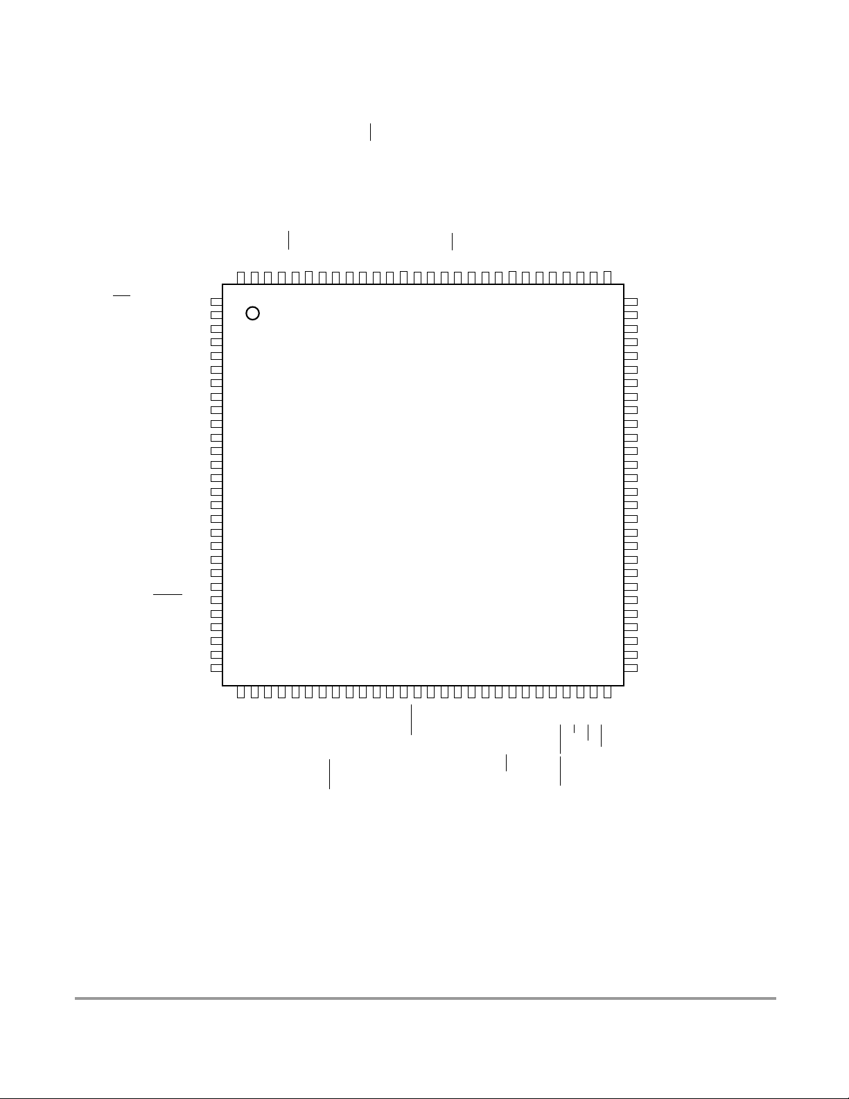
Device User Guide — 9S12DT128DGV2/D V02.16
ECS/ROMCTL
PP4/KWP4/PWM4
PP5/KWP5/PWM5
PP6/KWP6/PWM6
PP7/KWP7/PWM7
PK7/
VDDX
VSSX
PM0/RXCAN0/RXB
PM1/TXCAN0/TXB
PM2/RX_BF/RXCAN1/RXCAN0/MISO0
PM3/TX_BF/TXCAN1/TXCAN0/SS0
PM4/BF_PSYN/RXCAN0/RXCAN4/MOSI0
PM5/BF_PROK/TXCAN0/TXCAN4/SCK0
PJ6/KWJ6/RXCAN4/SDA/RXCAN0
PJ7/KWJ7/TXCAN4/SCL/TXCAN0
VREGEN
PS7/SS0
PS6/SCK0
PS5/MOSI0
PS4/MISO0
PS3/TXD1
PS2/RXD1
PS1/TXD0
PS0/RXD0
PM6/BF_PERR/RXCAN4
PM7/BF_PSLM/TXCAN4
VSSA
VRL
SS1/PWM3/KWP3/PP3
SCK1/PWM2/KWP2/PP2
MOSI1/PWM1/KWP1/PP1
MISO1/PWM0/KWP0/PP0
XADDR17/PK3
XADDR16/PK2
XADDR15/PK1
XADDR14/PK0
IOC0/PT0
IOC1/PT1
IOC2/PT2
IOC3/PT3
VDD1
VSS1
IOC4/PT4
IOC5/PT5
IOC6/PT6
IOC7/PT7
XADDR19/PK5
XADDR18/PK4
KWJ1/PJ1
KWJ0/PJ0
MODC/TAGHI/BKGD
ADDR0/DATA0/PB0
ADDR1/DATA1/PB1
ADDR2/DATA2/PB2
ADDR3/DATA3/PB3
ADDR4/DATA4/PB4
112
111
110
109
108
107
106
105
104
1
2
3
4
5
6
7
8
9
10
11
12
13
14
15
16
17
18
19
20
21
22
23
24
25
26
27
28
293031323334353637383940414243444546474849505152535455
MC9S12DT128E, MC9S12DT128, MC9S12DG128E,
MC9S12DG128, MC9S12DJ128E, MC9S12DJ128,
MC9S12DB128, MC9S12A128, SC515846, SC515847,
SC515848, SC515849, SC101161DT, SC101161DG,
SC101161DJ, SC102202, SC102203, SC102204,
103
999897969594939291908988878685
102
101
100
SC102205
112LQFP
84
VRH
83
VDDA
82
PAD15/AN15/ETRIG1
81
PAD07/AN07/ETRIG0
80
PAD14/AN14
79
PAD06/AN06
78
PAD13/AN13
77
PAD05/AN05
76
PAD12/AN12
75
PAD04/AN04
74
PAD11/AN11
73
PAD03/AN03
72
PAD10/AN10
71
PAD02/AN02
70
PAD09/AN09
69
PAD01/AN01
68
PAD08/AN08
67
PAD00/AN00
66
VSS2
65
VDD2
64
PA7/ADDR15/DATA15
63
PA6/ADDR14/DATA14
62
PA5/ADDR13/DATA13
61
PA4/ADDR12/DATA12
60
PA3/ADDR11/DATA11
59
PA2/ADDR10/DATA10
58
PA1/ADDR9/DATA9
57
PA0/ADDR8/DATA8
56
XFC
XTAL
VSSR
VDDR
RESET
KWH7/PH7
KWH6/PH6
KWH5/PH5
KWH4/PH4
ADDR5/DATA5/PB5
ADDR6/DATA6/PB6
ADDR7/DATA7/PB7
Signals shown in Bold are not available on all the 80 pin package options
Signals shown in Bold-Italics are not available on the MC9S12DJ128E, MC9S12DJ128, MC9S12DG128E, MC9S12DG128, MC9S12A128,
SC515847, SC515848, SC101161DG, SC101161DJ, SC102203, and SC102204 80 pin package options
Signals shown in Italics are not available on the MC9S12DB128, SC515846, and SC102202 80 pin package options
ECLK/PE4
MODA/IPIPE0/PE5
MODB/IPIPE1/PE6
XCLKS/NOACC/PE7
VDDPLL
EXTAL
VSSPLL
TEST
SS1/KWH3/PH3
SCK1/KWH2/PH2
MOSI1/KWH1/PH1
IRQ/PE1
R/W/PE2
XIRQ/PE0
MISO1/KWH0/PH0
LSTRB/TAGLO/PE3
Figure 2-1 Pin assignments 112 LQFP for MC9S12DT128E, MC9S12DT128,
MC9S12DG128E, MC9S12DG128, MC9S12DJ128E, MC9S12DJ128, MC9S12DB128
MC9S12A128, SC515846, SC515847, SC515848, SC515849, SC101161DT, SC101161DG,
SC101161DJ, SC102202, SC102203, SC102204, and SC102205
58
Freescale Semiconductor
Page 59
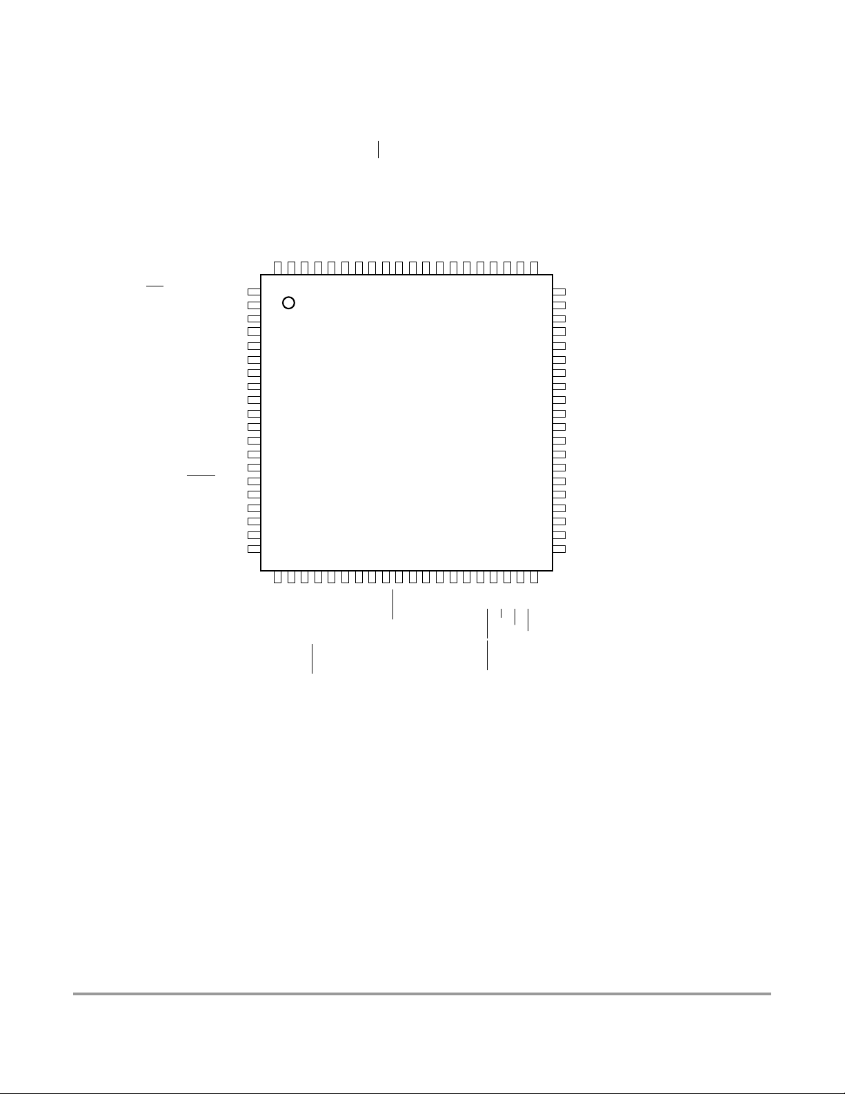
PP4/KWP4/PWM4
PP5/KWP5/PWM5
PP7/KWP7/PWM7
VDDX
VSSX
PM0/RXCAN0/RXB
PM1/TXCAN0/TXB
PM2/RXCAN1/RXCAN0/MISO0
PM3/TXCAN1/TXCAN0/SS0
PM4/RXCAN0/RXCAN4/MOSI0
PM5/TXCAN0/TXCAN4/SCK0
PJ6/KWJ6/RXCAN4/SDA/RXCAN0
Device User Guide — 9S12DT128DGV2/D V02.16
PJ7/KWJ7/TXCAN4/SCL/TXCAN0
VREGEN
PS3/TXD1
PS2//RXD1
PS1/TXD0
PS0/RXD0
VSSA
VRL
SS1/PWM3/KWP3/PP3
SCK1/PWM2/KWP2/PP2
MOSI1/PWM1/KWP1/PP1
MISO1/PWM0/KWP0/PP0
IOC0/PT0
IOC1/PT1
IOC2/PT2
IOC3/PT3
VDD1
VSS1
IOC4/PT4
IOC5/PT5
IOC6/PT6
IOC7/PT7
MODC/TAGHI/BKGD
ADDR0/DATA0/PB0
ADDR1/DATA1/PB1
ADDR2/DATA2/PB2
ADDR3/DATA3/PB3
ADDR4/DATA4/PB4
80797877767574737271706968676665646362
1
2
3
4
5
6
7
8
9
10
11
12
13
14
15
16
17
18
19
20
21222324252627282930313233343536373839
ADDR5/DATA5/PB5
MC9S12DG128E, MC9S12DG128,
MC9S12DJ128E, MC9S12DJ128,
MC9S12A128, SC515847,
SC515848, SC101161DG,
SC101161DJ, SC102203, SC102204
80 QFP
VDDR
RESET
XFC
VDDPLL
VSSPLL
ADDR6/DATA6/PB6
ADDR7/DATA7/PB7
XCLKS/NOACC/PE7
VSSR
ECLK/PE4
MODA/IPIPE0/PE5
MODB/IPIPE1/PE6
EXTAL
XTAL
TEST
IRQ/PE1
R/W/PE2
LSTRB/TAGLO/PE3
61
60
VRH
59
VDDA
58
PAD07/AN07/ETRIG0
57
PAD06/AN06
56
PAD05/AN05
55
PAD04/AN04
54
PAD03/AN03
53
PAD02/AN02
52
PAD01/AN01
51
PAD00/AN00
50
VSS2
49
VDD2
48
PA7/ADDR15/DATA15
47
PA6/ADDR14/DATA14
46
PA5/ADDR13/DATA13
45
PA4/ADDR12/DATA12
44
PA3/ADDR11/DATA11
43
PA2/ADDR10/DATA10
42
PA1/ADDR9/DATA9
41
PA0/ADDR8/DATA8
40
XIRQ/PE0
Figure 2-2 Pin Assignments in 80 QFP for MC9S12DG128E, MC9S12DG128,
MC9S12DJ128E, MC9S12DJ128, MC9S12A128, SC515847, SC515848, SC101161DG,
SC101161DJ, SC102203, and SC102204 Bondout
Freescale Semiconductor
59
Page 60

Device User Guide — 9S12DT128DGV2/D V02.16
PP4/KWP4/PWM4
PP5/KWP5/PWM5
PP7/KWP7/PWM7
VDDX
VSSX
PM2/RX_BF
PM3/TX_BF
PM4/BF_PSYN
PM5/BF_PROK
VREGEN
PS7/SS0
PS6/SCK0
PS5/MOSI0
PS4/MISO0
PS1/TXD0
PS0/RXD0
PM6/BF_PERR
PM7/BF_PSLM
VSSA
VRL
SS1/PWM3/KWP3/PP3
SCK1/PWM2/KWP2/PP2
MOSI1/PWM1/KWP1/PP1
MISO1/PWM0/KWP0/PP0
IOC0/PT0
IOC1/PT1
IOC2/PT2
IOC3/PT3
VDD1
VSS1
IOC4/PT4
IOC5/PT5
IOC6/PT6
IOC7/PT7
MODC/TAGHI/BKGD
ADDR0/DATA0/PB0
ADDR1/DATA1/PB1
ADDR2/DATA2/PB2
ADDR3/DATA3/PB3
ADDR4/DATA4/PB4
80797877767574737271706968676665646362
1
2
3
4
5
6
7
8
9
10
11
12
13
14
15
16
17
18
19
20
21222324252627282930313233343536373839
ADDR5/DATA5/PB5
ADDR6/DATA6/PB6
MC9S12DB128, SC515846,
SC102202
80 QFP
VSSR
VDDR
RESET
MODA/IPIPE0/PE5
MODB/IPIPE1/PE6
ADDR7/DATA7/PB7
XCLKS/NOACC/PE7
ECLK/PE4
XFC
VDDPLL
EXTAL
VSSPLL
XTAL
TEST
IRQ/PE1
R/W/PE2
LSTRB/TAGLO/PE3
61
60
VRH
59
VDDA
58
PAD07/AN07/ETRIG0
57
PAD06/AN06
56
PAD05/AN05
55
PAD04/AN04
54
PAD03/AN03
53
PAD02/AN02
52
PAD01/AN01
51
PAD00/AN00
50
VSS2
49
VDD2
48
PA7/ADDR15/DATA15
47
PA6/ADDR14/DATA14
46
PA5/ADDR13/DATA13
45
PA4/ADDR12/DATA12
44
PA3/ADDR11/DATA11
43
PA2/ADDR10/DATA10
42
PA1/ADDR9/DATA9
41
PA0/ADDR8/DATA8
40
XIRQ/PE0
Figure 2-3 Pin Assignments in 80 QFP for MC9S12DB128, SC515846, and SC102202
Bondout
2.2 Signal Properties Summary
(Table 2-1) summarizes the pin functionality. Signals shown in Bold are not available on all the 80-pin
package options. Signals shown in Bold-Italics are not available on the MC9S12DG128E,
MC9S12DG128, MC9S12DJ128E, MC9S12DJ128, MC9S12A128, SC515847, SC515848,
SC101161DG, SC101161DJ, SC102203, and SC102204 80-pin package options. Signals shown in Italics
are not available on MC9S12DB128, SC515846, and SC102202 80-pin package options.
60
Freescale Semiconductor
Page 61

Device User Guide — 9S12DT128DGV2/D V02.16
Table 2-1 Signal Properties
Internal Pull
Pin Name
Function 1
EXTAL————VDDPLL NA NA
XTAL————VDDPLL NA NA
RESET ————VDDR None None External Reset
TEST ————N.A. None None Test Input
VREGEN ————VDDX NA NA
XFC————VDDPLL NA NA PLL Loop Filter
BKGD
PAD[15] AN1[7] ETRIG1 — — VDDA None None
PAD[14:8] AN1[6:0] — — — VDDA None None
PAD[7] AN0[7] ETRIG0 — — VDDA None None
PAD[6:0] AN0[6:0] — — — VDDA None None
PA[7:0]
PB[7:0]
PE7 NOACC
PE6 IPIPE1 MODB — — VDDR
PE5 IPIPE0 MODA — — VDDR
PE4 ECLK — — — VDDR
PE3
PE2 R/
PE1
PE0
PH7 KWH7 --- — — VDDR
Pin Name
Function 2
TAGHI MODC — — VDDR
ADDR[15:8]/
DATA[15:8]
ADDR[7:0]/
DATA[7:0]
LSTRB TAGLO — — VDDR
W — — — VDDR
IRQ — — — VDDR
XIRQ — — — VDDR
Pin Name
Function 3
— — — VDDR
— — — VDDR
XCLKS — — VDDR
Pin Name
Function 4
Pin Name
Function 5
Powered
by
Resistor
CTRL
Always
Up
PUCR/
PUPAE
PUCR/
PUPBE
PUCR/
PUPEE
While RESET pin
PUCR/
PUPEE
PERH/
PPSH
Reset
State
Up
Disabled
Disabled
Mode
depen-
dant
low:
Down
Mode
depen-
dant
Up
Disabled Port H I/O, Interrupt
Description
Oscillator Pins
Voltage Regulator
Enable Input
Background Debug,
Tag High, Mode Input
Port AD Input,
Analog Inputs,
External Trigger
Input (ATD1)
Port AD Input,
Analog Inputs
(ATD1)
Port AD Input, Analog
Inputs, External
Trigger Input (ATD0)
Port AD Input, Analog
Inputs (ATD0)
Port A I/O,
Multiplexed
Address/Data
Port B I/O,
Multiplexed
Address/Data
Port E I/O, Access,
Clock Select
1
Port E I/O, Pipe
Status, Mode Input
Port E I/O, Pipe
Status, Mode Input
Port E I/O, Bus Clock
Output
Port E I/O, Byte
Strobe, Tag Low
1
Port E I/O, R/
expanded modes
Port E Input,
Maskable Interrupt
Port E Input, Non
Maskable Interrupt
W in
Freescale Semiconductor
61
Page 62

Device User Guide — 9S12DT128DGV2/D V02.16
Pin Name
Function 1
PH6 KWH6 --- — — VDDR
PH5 KWH5 --- — — VDDR
PH4 KWH4 --- — — VDDR
PH3 KWH3
PH2 KWH2 SCK1 — — VDDR
PH1 KWH1 MOSI1 — — VDDR
PH0 KWH0 MISO1 — — VDDR
PJ7 KWJ7 TXCAN4 SCL TXCAN0 VDDX
PJ6 KWJ6 RXCAN4 SDA RXCAN0 VDDX
PJ[1:0] KWJ[1:0] — — — VDDX
PK7
PK[5:0]
PM7 BF_PSLM TXCAN4 — — VDDX
PM6 BF_PERR RXCAN4 — — VDDX
PM5 BF_PROK TXCAN0 TXCAN4 SCK0 VDDX
PM4 BF_PSYN RXCAN0 RXCAN4 MOSI0 VDDX
PM3 TX_BF TXCAN1 TXCAN0
PM2 RX_BF RXCAN1 RXCAN0 MISO0 VDDX
Pin Name
Function 2
ECS ROMCTL ——VDDX
XADDR[19:
14]
Pin Name
Function 3
SS1 — — VDDR
———VDDX
Pin Name
Function 4
Pin Name
Function 5
SS0 VDDX
Powered
by
Internal Pull
Resistor
CTRL
PERH/
PPSH
PERH/
PPSH
PERH/
PPSH
PERH/
PPSH
PERH/
PPSH
PERH/
PPSH
PERH/
PPSH
PERJ/
PPSJ
PERJ/
PPSJ
PERJ/
PPSJ
PUCR/
PUPKE
PUCR/
PUPKE
PERM/
PPSM
PERM/
PPSM
PERM/
PPSM
PERM/
PPSM
PERM/
PPSM
PERM/
PPSM
Reset
State
Disabled Port H I/O, Interrupt
Disabled Port H I/O, Interrupt
Disabled Port H I/O, Interrupt
Disabled
Disabled
Disabled
Disabled
Up
Up
Up Port J I/O, Interrupts
Up
Up
Disabled
Disabled
Disabled
Disabled
Disabled
Disabled
Description
Port H I/O, Interrupt,
SS of SPI1
Port H I/O, Interrupt,
SCK of SPI1
Port H I/O, Interrupt,
MOSI of SPI1
Port H I/O, Interrupt,
MISO of SPI1
Port J I/O, Interrupt,
TX of CAN4, SCL of
IIC
Port J I/O, Interrupt,
RX of CAN4, SDA of
IIC
Port K I/O,
Emulation Chip
Select, ROM Control
Port K I/O, Extended
Addresses
Port M I/O, BF slot
mismatch pulse, TX
of CAN4
Port M I/O,BF illegal
pulse/message
format error pulse,
RX of CAN4
Port M I/O, BF
reception ok pulse,
TX of CAN0, CAN4,
SCK of SPI0
Port M I/O, BF sync
pulse (Rx/Tx) OK
pulse o/p, RX of
CAN0, CAN4, MOSI
of SPI0
Port M I/O, TX of BF,
CAN1, CAN0, SS of
SPI0
Port M I/O, RX of BF,
CAN1, CAN0, MISO
of SPI0
62
Freescale Semiconductor
Page 63

Device User Guide — 9S12DT128DGV2/D V02.16
Internal Pull
Pin Name
Function 1
PM1 TXCAN0 TXB — — VDDX
PM0 RXCAN0 RXB — — VDDX
PP7 KWP7 PWM7 — — VDDX
PP6 KWP6 PWM6 — — VDDX
PP5 KWP5 PWM5 — — VDDX
PP4 KWP4 PWM4 — — VDDX
PP3 KWP3 PWM3
PP2 KWP2 PWM2 SCK1 — VDDX
PP1 KWP1 PWM1 MOSI1 — VDDX
PP0 KWP0 PWM0 MISO1 — VDDX
PS7
PS6 SCK0 — — — VDDX
PS5 MOSI0 — — — VDDX
PS4 MISO0 — — — VDDX
PS3 TXD1 — — — VDDX
PS2 RXD1 — — — VDDX
PS1 TXD0 — — — VDDX
PS0 RXD0 — — — VDDX
PT[7:0] IOC[7:0] — — — VDDX
NOTES:
1. Refer to PEAR register description in HCS12 Multiplexed External Bus Interface (MEBI) Block Guide.
Pin Name
Function 2
SS0 — — — VDDX
Pin Name
Function 3
Pin Name
Function 4
SS1 — VDDX
Pin Name
Function 5
Powered
by
Resistor
CTRL
PERM/
PPSM
PERM/
PPSM
PERP/
PPSP
PERP/
PPSP
PERP/
PPSP
PERP/
PPSP
PERP/
PPSP
PERP/
PPSP
PERP/
PPSP
PERP/
PPSP
PERS/
PPSS
PERS/
PPSS
PERS/
PPSS
PERS/
PPSS
PERS/
PPSS
PERS/
PPSS
PERS/
PPSS
PERS/
PPSS
PERT/
PPST
Reset
State
Disabled
Disabled
Disabled
Disabled
Disabled
Disabled
Disabled
Disabled
Disabled
Disabled
Up
Up
Up
Up
Up
Up
Up
Up
Disabled
Description
Port M I/O, TX of
CAN0, RX of BDLC
Port M I/O, RX of
CAN0, RX of BDLC
Port P I/O, Interrupt,
Channel 7 of PWM
Port P I/O, Interrupt,
Channel 6 of PWM
Port P I/O, Interrupt,
Channel 5 of PWM
Port P I/O, Interrupt,
Channel 4 of PWM
Port P I/O, Interrupt,
Channel 3 of PWM,
SS of SPI1
Port P I/O, Interrupt,
Channel 2 of PWM,
SCK of SPI1
Port P I/O, Interrupt,
Channel 1 of PWM,
MOSI of SPI1
Port P I/O, Interrupt,
Channel 0 of PWM,
MISO2 of SPI1
Port S I/O,
SPI0
Port S I/O, SCK of
SPI0
Port S I/O, MOSI of
SPI0
Port S I/O, MISO of
SPI0
Port S I/O, TXD of
SCI1
Port S I/O, RXD of
SCI1
Port S I/O, TXD of
SCI0
Port S I/O, RXD of
SCI0
Port T I/O, Timer
channels
SS of
Freescale Semiconductor
63
Page 64
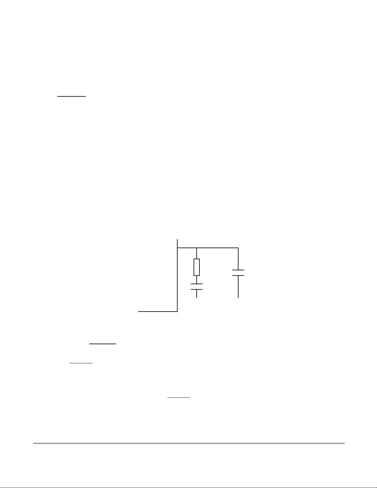
Device User Guide — 9S12DT128DGV2/D V02.16
2.3 Detailed Signal Descriptions
2.3.1 EXTAL, XTAL — Oscillator Pins
EXTAL and XTAL are the crystal driverand external clock pins. On reset all the device clocksare derived
from the EXTAL input frequency. XTAL is the crystal output.
2.3.2 RESET — External Reset Pin
An active low bidirectional control signal, it acts as an input to initialize the MCU to a known start-up
state, and an output when an internal MCU function causes a reset.
2.3.3 TEST — Test Pin
This input only pin is reserved for test.
NOTE: The TEST pin must be tied to VSS in all applications.
2.3.4 XFC — PLL Loop Filter Pin
PLL loop filter. Please ask your Freescale representative for the interactive application note to compute
PLL loop filter elements. Any current leakage on this pin must be avoided.
XFC
MCU
R
C
S
C
P
VDDPLLVDDPLL
Figure 2-4 PLL Loop Filter Connections
2.3.5 BKGD / TAGHI / MODC — Background Debug, Tag High, and Mode Pin
The BKGD/TAGHI/MODC pin is used as a pseudo-open-drain pin for the background debug
communication. In MCU expanded modes of operation when instruction tagging is on, an input low on
this pin during the falling edge of E-clock tags the high half of the instruction word being read into the
instruction queue. It is used as a MCU operating mode select pin during reset. The state of this pin is
latched to the MODC bit at the rising edge of
RESET. This pin has a permanently enabled pull-up device.
64
Freescale Semiconductor
Page 65

Device User Guide — 9S12DT128DGV2/D V02.16
2.3.6 PAD[15] / AN1[7] / ETRIG1 — Port AD Input Pin [15]
PAD15 is a general purpose input pin and analog input of the analog to digital converter ATD1. It can act
as an external trigger input for the ATD1.
2.3.7 PAD[14:8] / AN1[6:0] — Port AD Input Pins [14:8]
PAD14 - PAD8 are general purpose input pins and analog inputs of the analog to digital converter ATD1.
2.3.8 PAD[7] / AN0[7] / ETRIG0 — Port AD Input Pin [7]
PAD7 is a general purpose input pin and analog input of the analog to digital converter ATD0. It can act
as an external trigger input for the ATD0.
2.3.9 PAD[6:0] / AN0[6:0] — Port AD Input Pins [6:0]
PAD6 - PAD8 are general purpose input pins and analog inputs of the analog to digital converter ATD0.
2.3.10 PA[7:0] / ADDR[15:8] / DATA[15:8] — Port A I/O Pins
PA7-PA0 are general purpose input or output pins. In MCU expanded modes of operation, these pins are
used for the multiplexed external address and data bus.
2.3.11 PB[7:0] / ADDR[7:0] / DATA[7:0] — Port B I/O Pins
PB7-PB0 are general purpose input or output pins. In MCU expanded modes of operation, these pins are
used for the multiplexed external address and data bus.
2.3.12 PE7 / NOACC / XCLKS — Port E I/O Pin 7
PE7 is a general purpose input or output pin. During MCU expanded modes of operation, the NOACC
signal, when enabled, is used to indicate that the current bus cycle is an unused or “free” cycle. This signal
will assert when the CPU is not using the bus.
XCLKS is an input signal which controls whether a crystal in combination with the internal Colpitts
The
(low power) oscillator is used or whether Pierce oscillator/external clock circuitry is used. The state of this
pin is latched at the rising edge of
external clock drive. Ifinput is a logic high an oscillator circuit is configured onEXTAL and XTAL. Since
this pin is an input with a pull-up device during reset, if the pin is left floating, the default configuration is
an oscillator circuit on EXTAL and XTAL.
RESET. If the input is a logic low the EXTAL pin is configured for an
Freescale Semiconductor
65
Page 66
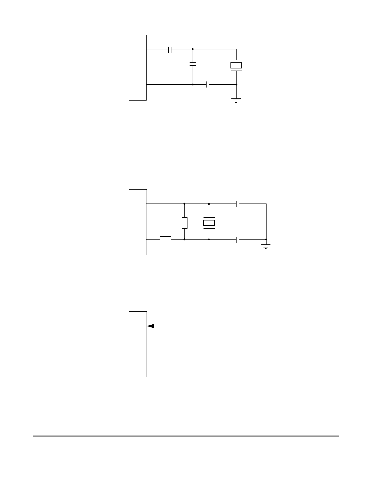
Device User Guide — 9S12DT128DGV2/D V02.16
EXTAL
CDC*
MCU
XTAL
* Due to the nature of a translated ground Colpitts oscillator a
DC voltage bias is applied to the crystal
Please contact the crystal manufacturer for crystal DC
bias conditions and recommended capacitor value CDC.
Figure 2-5 Colpitts Oscillator Connections (PE7=1)
C
1
Crystal or
ceramic resonator
C
2
VSSPLL
EXTAL
C
1
MCU
XTAL
R
B
*
R
S
Crystal or
ceramic resonator
C
2
VSSPLL
* Rs can be zero (shorted) when used with higher frequency crystals.
Refer to manufacturer’s data.
Figure 2-6 Pierce Oscillator Connections (PE7=0)
MCU
EXTAL
XTAL
not connected
CMOS-COMPATIBLE
EXTERNAL OSCILLATOR
(VDDPLL-Level)
66
Figure 2-7 External Clock Connections (PE7=0)
Freescale Semiconductor
Page 67

Device User Guide — 9S12DT128DGV2/D V02.16
2.3.13 PE6 / MODB / IPIPE1 — Port E I/O Pin 6
PE6 is a general purpose input or output pin. It is used as a MCU operating mode select pin during reset.
The state of this pin is latched to the MODB bit at the rising edge of
instruction queue tracking signal IPIPE1. This pin is an input with a pull-down device which is only active
RESET is low.
when
RESET. This pin is shared with the
2.3.14 PE5 / MODA / IPIPE0 — Port E I/O Pin 5
PE5 is a general purpose input or output pin. It is used as a MCU operating mode select pin during reset.
The state of this pin is latched to the MODA bit at the rising edge of
instruction queue tracking signal IPIPE0. This pin is an input with a pull-down device which is only active
RESET is low.
when
RESET. This pin is shared with the
2.3.15 PE4 / ECLK — Port E I/O Pin 4
PE4 is a general purpose input or output pin. It can be configured to drive the internal bus clock ECLK.
ECLK can be used as a timing reference.
2.3.16 PE3 / LSTRB / TAGLO — Port E I/O Pin 3
PE3 is a general purpose input or output pin. In MCU expanded modes of operation, LSTRB can be used
for the low-byte strobe function to indicate the type of bus access and when instruction tagging is on,
TAGLO is used to tag the low half of the instruction word being read into the instruction queue.
2.3.17 PE2 / R/W— Port E I/O Pin 2
PE2 is a general purpose input or output pin. In MCU expanded modes of operations, this pin drives the
read/write output signal for the external bus. It indicates the direction of data on the external bus.
2.3.18 PE1 / IRQ — Port E Input Pin 1
PE1 is a general purpose input pin and the maskable interrupt request input that provides a means of
applying asynchronous interrupt requests. This will wake up the MCU from STOP or WAIT mode.
2.3.19 PE0 / XIRQ — Port E Input Pin 0
PE0 is a general purpose input pin and the non-maskable interrupt request input that provides a means of
applying asynchronous interrupt requests. This will wake up the MCU from STOP or WAIT mode.
2.3.20 PH7 / KWH7 — Port H I/O Pin 7
PH7is a general purpose inputoroutput pin. It can be configuredto generate an interrupt causing theMCU
to exit STOP or WAIT mode.
Freescale Semiconductor
67
Page 68

Device User Guide — 9S12DT128DGV2/D V02.16
2.3.21 PH6 / KWH6 — Port H I/O Pin 6
PH6is a general purpose inputoroutput pin. It can be configuredto generate an interrupt causing theMCU
to exit STOP or WAIT mode.
2.3.22 PH5 / KWH5 — Port H I/O Pin 5
PH5is a general purpose inputoroutput pin. It can be configuredto generate an interrupt causing theMCU
to exit STOP or WAIT mode.
2.3.23 PH4 / KWH4 — Port H I/O Pin 2
PH4is a general purpose inputoroutput pin. It can be configuredto generate an interrupt causing theMCU
to exit STOP or WAIT mode.
2.3.24 PH3 / KWH3 / SS1 — Port H I/O Pin 3
PH3is a general purpose inputoroutput pin. It can be configuredto generate an interrupt causing theMCU
to exit STOP or WAIT mode. It can be configured as slave select pin
1 (SPI1).
SS of the Serial Peripheral Interface
2.3.25 PH2 / KWH2 / SCK1 — Port H I/O Pin 2
PH2is a general purpose inputoroutput pin. It can be configuredto generate an interrupt causing theMCU
toexit STOP or WAIT mode. It canbeconfigured as serial clock pin SCK of the SerialPeripheralInterface
1 (SPI1).
2.3.26 PH1 / KWH1 / MOSI1 — Port H I/O Pin 1
PH1is a general purpose inputoroutput pin. It can be configuredto generate an interrupt causing theMCU
to exit STOP or WAIT mode. It can be configured as master output (during master mode) or slave input
pin (during slave mode) MOSI of the Serial Peripheral Interface 1 (SPI1).
2.3.27 PH0 / KWH0 / MISO1 — Port H I/O Pin 0
PH0is a general purpose inputoroutput pin. It can be configuredto generate an interrupt causing theMCU
to exit STOP or WAIT mode. It can be configured as master input (during master mode) or slave output
(during slave mode) pin MISO of the Serial Peripheral Interface 1 (SPI1).
2.3.28 PJ7 / KWJ7 / TXCAN4 / SCL / TXCAN0 — PORT J I/O Pin 7
PJ7 is a general purpose input or output pin. It can be configured to generate an interrupt causing the MCU
to exit STOP or WAIT mode. It can be configured as the transmit pin TXCAN for the Motorola Scalable
Controller Area Network controller 0 or 4 (CAN0, CAN4) or the serial clock pin SCL of the IIC module.
68
Freescale Semiconductor
Page 69

Device User Guide — 9S12DT128DGV2/D V02.16
2.3.29 PJ6 / KWJ6 / RXCAN4 / SDA / RXCAN0 — PORT J I/O Pin 6
PJ6 is a general purpose input or output pin. It can be configured to generate an interrupt causing the MCU
to exit STOP or WAIT mode. It can be configured as the receive pin RXCAN for the Motorola Scalable
Controller Area Network controller 0 or 4 (CAN0, CAN4) or the serial data pin SDA of the IIC module.
2.3.30 PJ[1:0] / KWJ[1:0] — Port J I/O Pins [1:0]
PJ1 and PJ0 are general purpose input or output pins. They can be configured to generate an interrupt
causing the MCU to exit STOP or WAIT mode.
2.3.31 PK7 / ECS / ROMCTL — Port K I/O Pin 7
PK7 is a general purpose input or output pin. During MCU expanded modes of operation, this pin is used
as the emulation chip select output (
enable the Flash EEPROM memory in the memory map (ROMCTL). At the rising edge of
state of this pin is latched to the ROMON bit. For a complete list of modes refer to 4.2 Chip
Configuration Summary.
ECS). While configurating MCU expanded modes, this pin is used to
RESET, the
2.3.32 PK[5:0] / XADDR[19:14] — Port K I/O Pins [5:0]
PK5-PK0 are general purpose input or output pins. In MCU expanded modes of operation, these pins
provide the expanded address XADDR[19:14] for the external bus.
2.3.33 PM7 / BF_PSLM / TXCAN4 — Port M I/O Pin 7
PM7 is a general purpose input or output pin. It can be configured as the slot mismatch output pulse pin
of Byteflight. It can be configured as the transmit pin TXCAN of the Motorola Scalable Controller Area
Network controllers 4 (CAN4).
2.3.34 PM6 / BF_PERR / RXCAN4 — Port M I/O Pin 6
PM6 is a general purpose input or output pin. It can be configured as the illegal pulse or message format
error output pulse pin of Byteflight. It can be configured as the receive pin RXCAN of the Motorola
Scalable Controller Area Network controllers 4 (CAN4).
2.3.35 PM5 / BF_PROK / TXCAN0 / TXCAN4 / SCK0 — Port M I/O Pin 5
PM5 is a general purpose input or output pin. It can be configured as the reception OK output pulse pin of
Byteflight. It can be configured as the transmit pin TXCAN of the Motorola Scalable Controller Area
Network controllers 0 or 4 (CAN0 or CAN4). It can be configured as the serial clock pin SCK of the Serial
Peripheral Interface 0 (SPI0).
Freescale Semiconductor
69
Page 70

Device User Guide — 9S12DT128DGV2/D V02.16
2.3.36 PM4 / BF_PSYN / RXCAN0 / RXCAN4/ MOSI0 — Port M I/O Pin 4
PM4 is a general purpose input or output pin. It can be configured as the correct synchronisation pulse
reception/transmission output pulse pin of Byteflight. It can be configured as the receive pin RXCAN of
the Motorola Scalable Controller Area Network controllers 0 or 4 (CAN0 or CAN4). It can be configured
as the master output (during master mode) or slave input pin (during slave mode) MOSI
Peripheral Interface 0 (SPI0).
for the Serial
2.3.37 PM3 / TX_BF / TXCAN1 / TXCAN0 / SS0 — Port M I/O Pin 3
PM3 is a general purpose input or output pin. It can be configured as the transmit pinTX_BF of Byteflight.
It can be configured as the transmit pin TXCAN of the Motorola Scalable Controller Area Network
controllers 1 or 0 (CAN1 or CAN0). It can be configured as the slave select pin
Interface 0 (SPI0).
SS of the Serial Peripheral
2.3.38 PM2 / RX_BF / RXCAN1 / RXCAN0 / MISO0 — Port M I/O Pin 2
PM2 is a general purpose input or output pin. It can be configured as the receive pin RX_BF of Byteflight.
It can be configured as the receive pin RXCAN of the Motorola Scalable Controller Area Network
controllers 1 or 0(CAN1 or CAN0). It can be configuredas the master input (during master mode) or slave
output pin (during slave mode) MISO for the Serial Peripheral Interface 0 (SPI0).
2.3.39 PM1 / TXCAN0 / TXB — Port M I/O Pin 1
PM1 is a general purpose input or output pin. It can be configured as the transmit pin TXCAN of the
Motorola Scalable Controller Area Network controller 0 (CAN0). It can be configured as the transmit pin
TXB of the BDLC.
2.3.40 PM0 / RXCAN0 / RXB — Port M I/O Pin 0
PM0 is a general purpose input or output pin. It can be configured as the receive pin RXCAN of the
Motorola Scalable Controller Area Network controller 0 (CAN0). It can be configured as the receive pin
RXB of the BDLC.
2.3.41 PP7 / KWP7 / PWM7 — Port P I/O Pin 7
PP7 is a generalpurpose input or output pin. It canbe configured to generate an interrupt causing the MCU
to exit STOP or WAIT mode. It can be configured as Pulse Width Modulator (PWM) channel 7 output.
2.3.42 PP6 / KWP6 / PWM6 — Port P I/O Pin 6
PP6 is a generalpurpose input or output pin. It canbe configured to generate an interrupt causing the MCU
to exit STOP or WAIT mode. It can be configured as Pulse Width Modulator (PWM) channel 6 output.
70
Freescale Semiconductor
Page 71

Device User Guide — 9S12DT128DGV2/D V02.16
2.3.43 PP5 / KWP5 / PWM5 — Port P I/O Pin 5
PP5 is a generalpurpose input or output pin. It canbe configured to generate an interrupt causing the MCU
to exit STOP or WAIT mode. It can be configured as Pulse Width Modulator (PWM) channel 5 output.
2.3.44 PP4 / KWP4 / PWM4 — Port P I/O Pin 4
PP4 is a generalpurpose input or output pin. It canbe configured to generate an interrupt causing the MCU
to exit STOP or WAIT mode. It can be configured as Pulse Width Modulator (PWM) channel 4 output.
2.3.45 PP3 / KWP3 / PWM3 / SS1 — Port P I/O Pin 3
PP3 is a generalpurpose input or output pin. It canbe configured to generate an interrupt causing the MCU
to exit STOP or WAIT mode. It can be configured as Pulse Width Modulator (PWM) channel 3 output. It
can be configured as slave select pin
SS of the Serial Peripheral Interface 1 (SPI1).
2.3.46 PP2 / KWP2 / PWM2 / SCK1 — Port P I/O Pin 2
PP2 is a generalpurpose input or output pin. It canbe configured to generate an interrupt causing the MCU
to exit STOP or WAIT mode. It can be configured as Pulse Width Modulator (PWM) channel 2 output. It
can be configured as serial clock pin SCK of the Serial Peripheral Interface 1 (SPI1).
2.3.47 PP1 / KWP1 / PWM1 / MOSI1 — Port P I/O Pin 1
PP1 is a generalpurpose input or output pin. It canbe configured to generate an interrupt causing the MCU
to exit STOP or WAIT mode. It can be configured as Pulse Width Modulator (PWM) channel 1 output. It
can be configured as master output (during master mode) or slave input pin (during slave mode) MOSI of
the Serial Peripheral Interface 1 (SPI1).
2.3.48 PP0 / KWP0 / PWM0 / MISO1 — Port P I/O Pin 0
PP0 is a generalpurpose input or output pin. It canbe configured to generate an interrupt causing the MCU
to exit STOP or WAIT mode. It can be configured as Pulse Width Modulator (PWM) channel 0 output. It
can be configured as master input (during master mode) or slave output (during slave mode) pin MISO of
the Serial Peripheral Interface 1 (SPI1).
2.3.49 PS7 / SS0 — Port S I/O Pin 7
PS7 is a general purpose input or output pin. It can be configured as the slave select pin SS of the Serial
Peripheral Interface 0 (SPI0).
2.3.50 PS6 / SCK0 — Port S I/O Pin 6
PS6 is a general purpose input or output pin. It can be configured as the serial clock pin SCK of the Serial
Peripheral Interface 0 (SPI0).
Freescale Semiconductor
71
Page 72

Device User Guide — 9S12DT128DGV2/D V02.16
2.3.51 PS5 / MOSI0 — Port S I/O Pin 5
PS5 is a general purpose input or output pin. It can be configured as master output (during master mode)
or slave input pin (during slave mode) MOSI of the Serial Peripheral Interface 0 (SPI0).
2.3.52 PS4 / MISO0 — Port S I/O Pin 4
PS4 is a general purpose input or output pin. It can be configured as master input (during master mode) or
slave output pin (during slave mode) MOSI of the Serial Peripheral Interface 0 (SPI0).
2.3.53 PS3 / TXD1 — Port S I/O Pin 3
PS3 is a general purpose input or output pin. It can be configured as the transmit pin TXD of Serial
Communication Interface 1 (SCI1).
2.3.54 PS2 / RXD1 — Port S I/O Pin 2
PS2 is a general purpose input or output pin. It can be configured as the receive pin RXD of Serial
Communication Interface 1 (SCI1).
2.3.55 PS1 / TXD0 — Port S I/O Pin 1
PS1 is a general purpose input or output pin. It can be configured as the transmit pin TXD of Serial
Communication Interface 0 (SCI0).
2.3.56 PS0 / RXD0 — Port S I/O Pin 0
PS0 is a general purpose input or output pin. It can be configured as the receive pin RXD of Serial
Communication Interface 0 (SCI0).
2.3.57 PT[7:0] / IOC[7:0] — Port T I/O Pins [7:0]
PT7-PT0 are general purpose input or output pins. They can be configured as input capture or output
compare pins IOC7-IOC0 of the Enhanced Capture Timer (ECT).
2.4 Power Supply Pins
MC9S12DT128 power and ground pins are described below.
Table 2-2 MC9S12DT128 Power and Ground Connection Summary
Mnemonic
Pin Number
112-pin QFP
VDD1, 2 13, 65 2.5V
VSS1, 2 14, 66 0V
Nominal
Voltage
Description
Internal power and ground generated by internal regulator
72
Freescale Semiconductor
Page 73

Device User Guide — 9S12DT128DGV2/D V02.16
Mnemonic
Pin Number
112-pin QFP
VDDR 41 5.0V
VSSR 40 0V
VDDX 107 5.0V
VSSX 106 0V
VDDA 83 5.0V Operating voltage and ground for the analog-to-digital
VSSA 86 0V
VRL 85 0V
VRH 84 5.0V
VDDPLL 43 2.5V Provides operating voltage and ground for the Phased-Locked
VSSPLL 45 0V
VREGEN 97 5V Internal Voltage Regulator enable/disable
Nominal
Voltage
Description
External power and ground, supply to pin drivers and internal
voltage regulator.
External power and ground, supply to pin drivers.
converters and the reference for the internal voltage regulator,
allows the supply voltage to the A/D to be bypassed
independently.
Reference voltages for the analog-to-digital converter.
Loop. This allows the supply voltage to the PLL to be
bypassed independently. Internal power and ground
generated by internal regulator.
NOTE: All VSS pins must be connected together in the application.
2.4.1 VDDX,VSSX — Power & Ground Pins for I/O Drivers
External power and ground for I/O drivers. Because fast signal transitions place high, short-duration
current demands on the power supply, use bypass capacitors with high-frequency characteristics and place
them as close to the MCU as possible. Bypass requirements depend on how heavily the MCU pins are
loaded.
2.4.2 VDDR, VSSR — Power & Ground Pins for I/O Drivers & for Internal
Voltage Regulator
External power and ground for I/O drivers and input to the internal voltage regulator. Because fast signal
transitions place high, short-duration current demands on the power supply, use bypass capacitors with
high-frequency characteristics and place them as close to the MCU as possible. Bypass requirements
depend on how heavily the MCU pins are loaded.
2.4.3 VDD1, VDD2, VSS1, VSS2 — Internal Logic Power Supply Pins
Power is supplied to the MCU through VDD and VSS. Because fast signal transitions place high,
short-duration current demands on the power supply, use bypass capacitors with high-frequency
characteristics and place them as close to the MCU as possible. This 2.5V supply is derived from the
internal voltage regulator. There is no static load on those pins allowed. The internal voltage regulator is
turned off, if VREGEN is tied to ground.
NOTE: No load allowed except for bypass capacitors.
Freescale Semiconductor
73
Page 74

Device User Guide — 9S12DT128DGV2/D V02.16
2.4.4 VDDA, VSSA — Power Supply Pins for ATD and VREG
VDDA, VSSA are the power supply and ground input pins for the voltage regulator and the analog to
digital converter. It also provides the reference for the internal voltage regulator. This allows the supply
voltage to the ATD and the reference voltage to be bypassed independently.
2.4.5 VRH, VRL — ATD Reference Voltage Input Pins
VRH and VRL are the reference voltage input pins for the analog to digital converter.
2.4.6 VDDPLL, VSSPLL — Power Supply Pins for PLL
Provides operating voltage and ground for the Oscillator and the Phased-Locked Loop. This allows the
supply voltage to the Oscillator and PLL to be bypassed independently.This 2.5V voltage is generated by
the internal voltage regulator.
NOTE: No load allowed except for bypass capacitors.
2.4.7 VREGEN — On Chip Voltage Regulator Enable
Enables the internal 5V to 2.5V voltage regulator. If this pin is tied low, VDD1,2 and VDDPLL must be
supplied externally.
74
Freescale Semiconductor
Page 75

Device User Guide — 9S12DT128DGV2/D V02.16
Section 3 System Clock Description
3.1 Overview
The Clock and Reset Generator provides the internal clock signals for the core and all peripheral modules.
Figure 3-1 shows the clock connections from the CRG to all modules.
Consult the CRG Block User Guide for details on clock generation.
HCS12 CORE
BDM
CPU
MEBI
INT
Flash
RAM
MMC
BKP
core clock
EXTAL
XTAL
CRG
bus clock
oscillator clock
Figure 3-1 Clock Connections
EEPROM
ECT
ATD0, 1
PWM
SCI0, SCI1
SPI0, 1
CAN0, 1, 4
IIC
BDLC
PIM
BF
Freescale Semiconductor
75
Page 76

Device User Guide — 9S12DT128DGV2/D V02.16
76
Freescale Semiconductor
Page 77

Device User Guide — 9S12DT128DGV2/D V02.16
Section 4 Modes of Operation
4.1 Overview
Eight possible modes determine the operating configuration of the MC9S12DT128. Each mode has an
associated default memory map and external bus configuration controlled by a further pin.
Three low power modes exist for the device.
4.2 Chip Configuration Summary
The operating mode out of resetis determined by the statesof the MODC, MODB, andMODA pins during
reset ((Table 4-1)). The MODC, MODB, and MODA bits in the MODE register show the current
operating mode and provide limited mode switching during operation. The states of the MODC, MODB,
and MODA pins are latched into these bits on the rising edge of the reset signal. The ROMCTL signal
allows the setting of the ROMON bit in the MISC register thus controlling whether the internal Flash is
visible in the memory map. ROMON = 1 mean the Flash is visible in the memory map. The state of the
ROMCTL pin is latched into the ROMON bit in the MISC register on the rising edge of the reset signal.
Table 4-1 Mode Selection
BKGD =
MODC
000X1
001
0 1 0 X 0 Special Test (Expanded Wide), BDM allowed
011
1 0 0 X 1 Normal Single Chip, BDM allowed
101
110X1
111
PE6 =
MODB
PE5 =
MODA
PK7 =
ROMCTL
01
10
01
10
00
11
00
11
ROMON
Bit
Mode Description
Special Single Chip, BDM allowed and ACTIVE. BDM is
allowed in all other modes but a serial command is
required to make BDM active.
Emulation Expanded Narrow, BDM allowed
Emulation Expanded Wide, BDM allowed
Normal Expanded Narrow, BDM allowed
Special Peripheral; BDM allowed but bus operations
would cause bus conflicts (must not be used)
Normal Expanded Wide, BDM allowed
For further explanation on the modes refer to the HCS12 Multiplexed External Bus Interface Block Guide.
Table 4-2 Clock Selection Based on PE7
Freescale Semiconductor
PE7 = XCLKS Description
1 Colpitts Oscillator selected
0 Pierce Oscillator/external clock selected
77
Page 78

Device User Guide — 9S12DT128DGV2/D V02.16
Table 4-3 Voltage Regulator VREGEN
VREGEN Description
1 Internal Voltage Regulator enabled
0
Internal Voltage Regulator disabled, VDD1,2 and
VDDPLL must be supplied externally with 2.5V
4.3 Security
The device will make available a security feature preventing the unauthorized read and write of the
memory contents. This feature allows:
• Protection of the contents of FLASH,
• Protection of the contents of EEPROM,
• Operation in single-chip mode, No BDM possible
• Operation from external memory with internal FLASH and EEPROM disabled.
The user must be reminded that part of the security must lie with the user’s code. An extreme example
would be user’s code that dumps the contents of the internal program. This code would defeat the purpose
of security. At the same time the user may also wish to put a back door in the user’s program. An example
of this is the user downloads a key through the SCI which allows access to a programming routine that
updates parameters stored in EEPROM.
4.3.1 Securing the Microcontroller
Once the user has programmed the FLASH and EEPROM (if desired), the part can be secured by
programming the security bits located in the FLASH module. These non-volatile bits will keep the part
secured through resetting the part and through powering down the part.
The security byte resides in a portion of the Flash array.
Check the Flash Block User Guide for more details on the security configuration.
4.3.2 Operation of the Secured Microcontroller
4.3.2.1 Normal Single Chip Mode
This will be the most common usage of the secured part. Everything will appear the same as if the part was
not secured with the exception of BDM operation. The BDM operation will be blocked.
4.3.2.2 Executing from External Memory
The user may wish to execute from external space with a secured microcontroller. This is accomplished
by resetting directly into expanded mode. The internal FLASH and EEPROM will be disabled. BDM
operations will be blocked.
78
Freescale Semiconductor
Page 79

Device User Guide — 9S12DT128DGV2/D V02.16
4.3.3 Unsecuring the Microcontroller
In order to unsecure the microcontroller, the internal FLASH and EEPROM must be erased. This can be
done through an external program in expanded mode or via a .sequence of BDM commands. Unsecuring
is also possible via the Backdoor Key Access. Refer to Flash Block Guide for details.
Once the user has erased the FLASH and EEPROM, the part can be reset into special single chip mode.
This invokes a program that verifies the erasure of the internal FLASH and EEPROM. Once this program
completes,the user can erase and program theFLASHsecurity bits to the unsecured state. Thisisgenerally
done through the BDM, but the user could also change to expanded mode (by writing the mode bits
through the BDM) and jumping to an external program (again through BDM commands). Note that if the
part goes through a reset before the security bits are reprogrammed to the unsecure state, the part will be
secured again.
4.4 Low Power Modes
The microcontroller features three main low power modes. Consult the respective Block User Guide for
information on the module behavior in Stop, Pseudo Stop, and Wait Mode. An important source of
information about the clock system is the Clock and Reset Generator User Guide (CRG).
4.4.1 Stop
Executing the CPU STOP instruction stops all clocks and the oscillator thus putting the chip in fully static
mode. Wake up from this mode can be done via reset or external interrupts.
4.4.2 Pseudo Stop
This mode is entered by executing the CPU STOP instruction. In this mode the oscillator is still running
and the Real Time Interrupt (RTI) or Watchdog (COP) sub module can stay active. Other peripherals are
turned off. This mode consumes more current than the full STOP mode, but the wake up time from this
mode is significantly shorter.
4.4.3 Wait
This mode is entered by executing the CPU WAI instruction. In this mode the CPU will not execute
instructions.The internal CPU signals (address and databus)willbefully static. All peripherals stay active.
For further power consumption the peripherals can individually turn off their local clocks.
4.4.4 Run
Although this is not a low power mode, unused peripheral modules should not be enabled in order to save
power.
Freescale Semiconductor
79
Page 80

Device User Guide — 9S12DT128DGV2/D V02.16
80
Freescale Semiconductor
Page 81

Device User Guide — 9S12DT128DGV2/D V02.16
Section 5 Resets and Interrupts
5.1 Overview
Consult the Exception Processing section of the CPU Reference Manual for information on resets and
interrupts.
5.2 Vectors
5.2.1 Vector Table
(Table 5-1) lists interrupt sources and vectors in default order of priority.
Table 5-1 Interrupt Vector Locations
Vector Address Interrupt Source
$FFFE, $FFFF Reset None None –
$FFFC, $FFFD Clock Monitor fail reset None COPCTL (CME, FCME) –
$FFFA, $FFFB COP failure reset None COP rate select –
$FFF8, $FFF9 Unimplemented instruction trap None None –
$FFF6, $FFF7 SWI None None –
$FFF4, $FFF5 XIRQ / BF High Priority Sync Pulse X-Bit None / BFRIER (XSYNIE) –
$FFF2, $FFF3 IRQ I-Bit INTCR (IRQEN) $F2
$FFF0, $FFF1 Real Time Interrupt I-Bit CRGINT (RTIE) $F0
$FFEE, $FFEF Enhanced Capture Timer channel 0 I-Bit TIE (C0I) $EE
$FFEC, $FFED Enhanced Capture Timer channel 1 I-Bit TIE (C1I) $EC
$FFEA, $FFEB Enhanced Capture Timer channel 2 I-Bit TIE (C2I) $EA
$FFE8, $FFE9 Enhanced Capture Timer channel 3 I-Bit TIE (C3I) $E8
$FFE6, $FFE7 Enhanced Capture Timer channel 4 I-Bit TIE (C4I) $E6
$FFE4, $FFE5 Enhanced Capture Timer channel 5 I-Bit TIE (C5I) $E4
$FFE2, $FFE3 Enhanced Capture Timer channel 6 I-Bit TIE (C6I) $E2
$FFE0, $FFE1 Enhanced Capture Timer channel 7 I-Bit TIE (C7I) $E0
$FFDE, $FFDF Enhanced Capture Timer overflow I-Bit TSCR2 (TOF) $DE
$FFDC, $FFDD Pulse accumulator A overflow I-Bit PACTL (PAOVI) $DC
$FFDA, $FFDB Pulse accumulator input edge I-Bit PACTL (PAI) $DA
$FFD8, $FFD9 SPI0 I-Bit SPICR1 (SPIE, SPTIE) $D8
$FFD6, $FFD7 SCI0 I-Bit
$FFD4, $FFD5 SCI1 I-Bit
$FFD2, $FFD3 ATD0 I-Bit ATDCTL2 (ASCIE) $D2
$FFD0, $FFD1 ATD1 I-Bit ATDCTL2 (ASCIE) $D0
$FFCE, $FFCF Port J I-Bit
$FFCC, $FFCD Port H I-Bit PIEH (PIEH7-0) $CC
CCR
Mask
Local Enable
SCICR2
(TIE, TCIE, RIE, ILIE)
SCICR2
(TIE, TCIE, RIE, ILIE)
PIEJ
(PIEJ7, PIEJ6, PIEJ1, PIEJ0)
HPRIO Value
to Elevate
$D6
$D4
$CE
Freescale Semiconductor
81
Page 82

Device User Guide — 9S12DT128DGV2/D V02.16
$FFCA, $FFCB Modulus Down Counter underflow I-Bit MCCTL (MCZI) $CA
$FFC8, $FFC9 Pulse Accumulator B Overflow I-Bit PBCTL (PBOVI) $C8
$FFC6, $FFC7 CRG PLL lock I-Bit PLLCR (LOCKIE) $C6
$FFC4, $FFC5 CRG Self Clock Mode I-Bit PLLCR (SCMIE) $C4
$FFC2, $FFC3 BDLC I-Bit DLCBCR1 (IE) $C2
$FFC0, $FFC1 IIC Bus I-Bit IBCR (IBIE) $C0
$FFBE, $FFBF SPI1 I-Bit SPICR1 (SPIE, SPTIE) $BE
$FFBC, $FFBD
$FFBA, $FFBB EEPROM I-Bit ECNFG (CCIE, CBEIE) $BA
$FFB8, $FFB9 FLASH I-Bit FCNFG (CCIE, CBEIE) $B8
$FFB6, $FFB7 CAN0 wake-up I-Bit CANRIER (WUPIE) $B6
$FFB4, $FFB5 CAN0 errors I-Bit CANRIER (CSCIE, OVRIE) $B4
$FFB2, $FFB3 CAN0 receive I-Bit CANRIER (RXFIE) $B2
$FFB0, $FFB1 CAN0 transmit I-Bit CANTIER (TXEIE[2:0]) $B0
$FFAE, $FFAF CAN1 wake-up I-Bit CANRIER (WUPIE) $AE
$FFAC, $FFAD CAN1 errors I-Bit CANRIER (CSCIE, OVRIE) $AC
$FFAA, $FFAB CAN1 receive I-Bit CANRIER (RXFIE) $AA
$FFA8, $FFA9 CAN1 transmit I-Bit CANTIER (TXEIE[2:0]) $A8
$FFA6, $FFA7 BF Receive FIFO not empty I-Bit BFRIER (RCVFIE) $A6
$FFA4, $FFA5 BF receive I-Bit BFBUFCTL[15:0] (IENA) $A4
$FFA2, $FFA3 BF Synchronization I-Bit BFRIER (SYNAIE, SYNNIE) $A2
$FFA0, $FFA1 BF general I-Bit
$FF98, $FF9F
$FF96, $FF97 CAN4 wake-up I-Bit CANRIER (WUPIE) $96
$FF94, $FF95 CAN4 errors I-Bit CANRIER (CSCIE, OVRIE) $94
$FF92, $FF93 CAN4 receive I-Bit CANRIER (RXFIE) $92
$FF90, $FF91 CAN4 transmit I-Bit CANTIER (TXEIE[2:0]) $90
$FF8E, $FF8F Port P Interrupt I-Bit PIEP (PIEP7-0) $8E
$FF8C, $FF8D PWM Emergency Shutdown I-Bit PWMSDN (PWMIE) $8C
$FF80 to
$FF8B
Reserved
BFBUFCTL[15:0] (IENA),
BFGIER (OVRNIE, ERRIE,
SYNEIE, SYNLIE, ILLPIE,
LOCKIE, WAKEIE)
BFRIER (SLMMIE)
Reserved
Reserved
$A0
5.3 Effects of Reset
When a reset occurs, MCU registers and control bits are changed to known start-up states. Refer to the
respective module Block User Guides for register reset states.
5.3.1 I/O pins
Refer to the HCS12 Multiplexed External Bus Interface (MEBI) Block Guide for mode dependent pin
configuration of port A, B, E and K out of reset.
Refer to the PIM Block User Guide for reset configurations of all peripheral module ports.
82
Freescale Semiconductor
Page 83

Device User Guide — 9S12DT128DGV2/D V02.16
NOTE: For devices assembled in 80-pin QFP packages all non-bonded out pins should be
configured as outputs after reset in order to avoid current drawn from floating
inputs. Refer to Table 2-1 for affected pins.
5.3.2 Memory
Refer to Table 1-1 for locations of the memories depending on the operating mode after reset.
The RAM array is not automatically initialized out of reset.
Freescale Semiconductor
83
Page 84

Device User Guide — 9S12DT128DGV2/D V02.16
84
Freescale Semiconductor
Page 85

Device User Guide — 9S12DT128DGV2/D V02.16
Section 6 HCS12 Core Block Description
6.1 CPU Block Description
Consult the CPU Reference Manual for information on the CPU.
6.1.1 Device-specific information
When the CPU Reference Manual refers to cycles this is equivalent to Bus Clock periods. So 1 cycle is
equivalent to 1 Bus Clock period.
6.2 HCS12 Module Mapping Control (MMC) Block Description
Consult the MMC Block Guide for information on the HCS12 Module Mapping Control module.
6.2.1 Device-specific information
• INITEE
– Reset state: $01
– Bits EE11-EE15 are "Write once in Normal and Emulation modes and write anytime in Special
modes".
• PPAGE
– Reset state: $00
– Register is "Write anytime in all modes".
• MEMSIZ0
– Reset state: $13
• MEMSIZ1
– Reset state: $80
6.3 HCS12 Multiplexed External Bus Interface (MEBI) Block Description
Consult the MEBI Block Guide for information on HCS12 Multiplexed External Bus Interface module.
6.3.1 Device-specific information
• PUCR
– Reset state: $90
Freescale Semiconductor
85
Page 86

Device User Guide — 9S12DT128DGV2/D V02.16
6.4 HCS12 Interrupt (INT) Block Description
Consult the INT Block Guide for information on the HCS12 Interrupt module.
6.5 HCS12 Background Debug Module (BDM) Block Description
Consult the BDM Block Guide for information on the HCS12 Background Debug module.
6.5.1 Device-specific information
When the BDM Block Guide refers to alternate clock this is equivalent to oscillator clock.
6.6 HCS12 Breakpoint (BKP) Block Description
Consult the BKP Block Guide for information on the HCS12 Breakpoint module.
Section 7 Clock and Reset Generator (CRG) Block Description
Consult the CRG Block User Guide for information about the Clock and Reset Generator module.
7.1 Device-specific information
The Low Voltage Reset feature of the CRG is not available on this device.
Section 8 Oscillator (OSC) Block Description
Consult the OSC Block User Guide for information about the Oscillator module.
8.1 Device-specific information
The XCLKS input signal is active low (see 2.3.12 PE / NOACC / XCLKS — Port E I/O Pin 7).
Section 9 Enhanced Capture Timer (ECT) Block Description
86
Freescale Semiconductor
Page 87

Device User Guide — 9S12DT128DGV2/D V02.16
Consult the ECT_16B8C Block User Guide for information about the Enhanced Capture Timer
module.When the ECT_16B8C Block User Guide refers to freeze mode this is equivalent to active BDM
mode.
Section 10 Analog to Digital Converter (ATD) Block Description
There are two Analog to Digital Converters (ATD1 and ATD0) implemented on the MC9S12DT128.
Consult the ATD_10B8C Block User Guide for information about each Analog to Digital Converter
module. When the ATD_10B8C Block User Guide refers to freeze mode this is equivalent to active BDM
mode.
Section 11 Inter-IC Bus (IIC) Block Description
Consult the IIC Block User Guide for information about the Inter-IC Bus module.
Section 12 Serial Communications Interface (SCI) Block Description
There are two Serial Communications Interfaces (SCI1 and SCI0) implemented on the MC9S12DT128
device. Consult the SCI Block User Guide for information about each Serial Communications Interface
module.
Section 13 Serial Peripheral Interface (SPI) Block Description
There are two Serial Peripheral Interfaces (SPI1 and SPI0) implemented on MC9S12DT128. Consult the
SPI Block User Guide for information about each Serial Peripheral Interface module.
Section 14 J1850 (BDLC) Block Description
Consult the BDLC Block User Guide for information about the J1850 module.
Section 15 Byteflight (BF) Block Description
Consult the BF Block User Guide for information about the 10 Mbps Byteflight module.
Freescale Semiconductor
87
Page 88

Device User Guide — 9S12DT128DGV2/D V02.16
15.1 Device-specific information
The read-only Module Version Register (BFMVR) contains the current version number of $80.
Section 16 Pulse Width Modulator (PWM) Block Description
Consult the PWM_8B8C Block User Guide for information about the Pulse Width Modulator module.
When the PWM_8B8C Block User Guide refers to freeze mode this is equivalent to active BDM mode.
Section 17 Flash EEPROM 128K Block Description
Consult the FTS128K Block User Guide for information about the flash module.
Section 18 EEPROM 2K Block Description
Consult the EETS2K Block User Guide for information about the EEPROM module.
Section 19 RAM Block Description
This module supports single-cycle misaligned word accesses without wait states.
Section 20 MSCAN Block Description
There are three MSCAN modules (CAN4, CAN1 and CAN0) implemented on the MC9S12DT128.
Consult the MSCAN Block User Guide for information about the Motorola Scalable CAN Module.
Section 21 Port Integration Module (PIM) Block Description
Consult the PIM_9DTB128 Block User Guide for information about the Port Integration Module.
Section 22 Voltage Regulator (VREG) Block Description
Consult the VREG Block User Guide for information about the dual output linear voltage regulator.
88
Freescale Semiconductor
Page 89

Device User Guide — 9S12DT128DGV2/D V02.16
Section 23 Printed Circuit Board Layout Proposal
Table 23-1 Suggested External Component Values
Component Purpose Type Value
C1 VDD1 filter cap ceramic X7R 100 … 220nF
C2 VDD2 filter cap ceramic X7R 100 … 220nF
C3 VDDA filter cap ceramic X7R 100nF
C4 VDDR filter cap X7R/tantalum >= 100nF
C5 VDDPLL filter cap ceramic X7R 100nF
C6 VDDX filter cap X7R/tantalum >= 100nF
C7 OSC load cap
C8 OSC load cap
C9 / C
S
C10 / C
C11 / C
P
DC
R1 / R PLL loop filter res See PLL Specification chapter
R2 / R
B
R3 / R
S
Q1 Quartz
PLL loop filter cap
PLL loop filter cap
DC cutoff cap
See PLL specification chapter
Colpitts mode only, if recommended by
quartz manufacturer
Pierce mode only
The PCB must be carefully laid out to ensure proper operation of the voltage regulator as well as of the
MCU itself. The following rules must be observed:
• Every supply pair must be decoupled by a ceramic capacitor connected as near as possible to the
corresponding pins (C1 – C6).
• Central point of the ground star should be the VSSR pin.
• Use low ohmic low inductance connections between VSS1, VSS2 and VSSR.
• VSSPLL must be directly connected to VSSR.
• Keep traces of VSSPLL, EXTAL and XTAL as short as possible and occupied board area for C7,
C8, C11 and Q1 as small as possible.
• Do not place other signals or supplies underneath area occupied by C7, C8, C10 and Q1 and the
connection area to the MCU.
• Central power input should be fed in at the VDDA/VSSA pins.
Freescale Semiconductor
89
Page 90
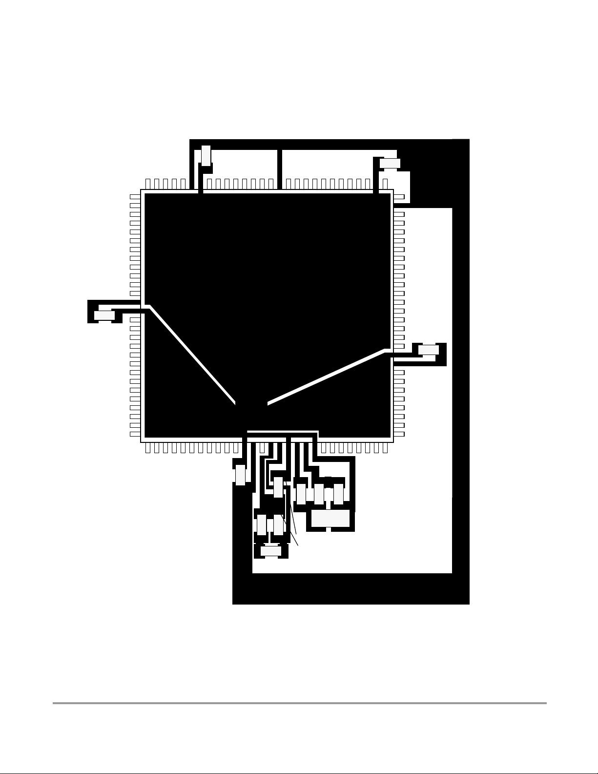
Device User Guide — 9S12DT128DGV2/D V02.16
Figure 23-1 Recommended PCB Layout for 112LQFP Colpitts Oscillator
C1
VDD1
VSS1
VDDX
C6
VSSX
VREGEN
VSSA
C3
VDDA
VSS2
C2
VDD2
90
VSSR
VDDR
C4
C9
R1
C5
C10
C8
C11
VSSPLL
VDDPLL
C7
Q1
Freescale Semiconductor
Page 91
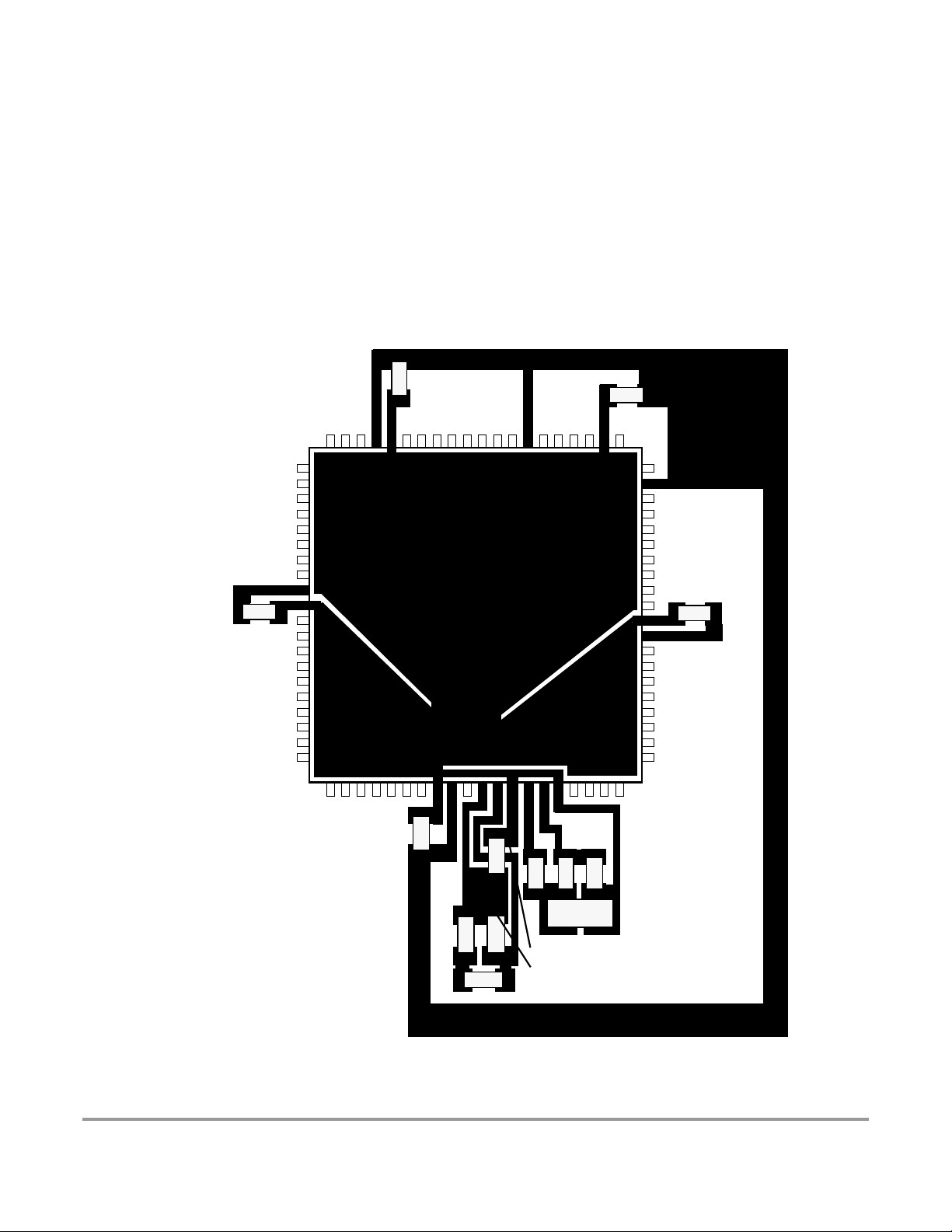
Device User Guide — 9S12DT128DGV2/D V02.16
Figure 23-2 Recommended PCB Layout for 80QFP (MC9S12DG128E, MC9S12DG128,
MC9S12DJ128E, MC9S12DJ128, MC9S12A128, SC515847, SC515848, SC101161DG,
SC101161DJ, SC102203, and SC102204) Colpitts Oscillator
VDDX
C6
VSSX
VREGEN
VSSA
C3
VDDA
C1
VDD1
VSS1
VSSR
VDDR
C4
C9
R1
C5
C10
C8
C11
VSSPLL
VDDPLL
VSS2
C2
VDD2
C7
Q1
Freescale Semiconductor
91
Page 92

Device User Guide — 9S12DT128DGV2/D V02.16
Figure 23-3 Recommended PCB Layout for 112LQFP Pierce Oscillator
C1
VDD1
VSS1
VDDX
C6
VSSX
VREGEN
VSSA
C3
VDDA
VSS2
C2
VDD2
VSSR
VDDR
VDDPLL
C4
C9
R1
C5
C10
C8
Q1
R2
R3
VSSPLL
C7
92
Freescale Semiconductor
Page 93

Device User Guide — 9S12DT128DGV2/D V02.16
Figure 23-4 Recommended PCB Layout for 80QFP (MC9S12DG128E, MC9S12DG128,
MC9S12DJ128E, MC9S12DJ128, MC9S12A128, SC515847, SC515848, SC101161DG,
SC101161DJ, SC102203, and SC102204) Pierce Oscillator
VDDX
C6
VSSX
VDD1
C1
VSS1
VREGEN
VSSA
C3
VDDA
VSS2
C2
VDD2
VSSR
VDDR
C4
C9
R1
C5
C10
R2
Q1
C8
VSSPLL
VDDPLL
VSSPLL
R3
C7
Freescale Semiconductor
93
Page 94
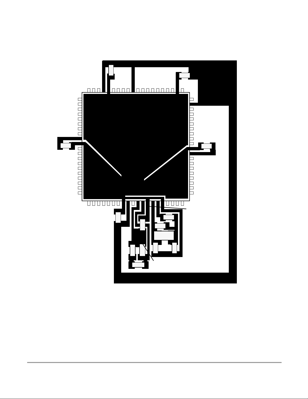
Device User Guide — 9S12DT128DGV2/D V02.16
Figure 23-5 Recommended PCB Layout for 80QFP (MC9S12DB128, SC515846, and
SC102202) Pierce Oscillator
VDDX
C6
VSSX
VDD1
C1
VSS1
VREGEN
VSSA
C3
VDDA
VSS2
C2
VDD2
VSSR
VDDR
C4
C9
R1
C5
C10
R2
Q1
C8
VSSPLL
VDDPLL
VSSPLL
R3
C7
94
Freescale Semiconductor
Page 95

Device User Guide — 9S12DT128DGV2/D V02.16
Freescale Semiconductor
95
Page 96

Device User Guide — 9S12DT128DGV2/D V02.16
96
Freescale Semiconductor
Page 97

Device User Guide — 9S12DT128DGV2/D V02.16
Appendix A Electrical Characteristics
A.1 General
This introduction is intended to give an overview on several common topics like power supply, current
injection etc.
A.1.1 Parameter Classification
The electrical parameters shown in this supplement are guaranteed by various methods. To give the
customer a better understanding the following classification is used and the parameters are tagged
accordingly in the tables where appropriate.
P:
Those parameters are guaranteed during production testing on each individual device.
C:
Those parameters are achieved by the design characterization by measuring a statistically relevant
sample size across process variations. They are regularly verified by production monitors.
T:
Those parameters are achieved by design characterization on a small sample size from typical
devices. All values shown in the typical column are within this category.
D:
Those parameters are derived mainly from simulations.
A.1.2 Power Supply
The MC9S12DT128 utilizes several pins to supply power to the I/O ports, A/D converter, oscillator, PLL
and internal logic.
The VDDA, VSSA pair supplies the A/D converter and the resistor ladder of the internal voltage regulator.
The VDDX, VSSX, VDDR and VSSR pairs supply the I/O pins, VDDR supplies also the internal voltage
regulator.
VDD1, VSS1, VDD2 and VSS2 are the supply pins for the digital logic, VDDPLL, VSSPLL supply the
oscillator and the PLL.
VSS1 and VSS2 are internally connected by metal.
VDDA, VDDX, VDDR as well as VSSA, VSSX, VSSR are connected by anti-parallel diodes for ESD
protection.
Freescale Semiconductor
97
Page 98

Device User Guide — 9S12DT128DGV2/D V02.16
NOTE: In the following context VDD5 is used for either VDDA, VDDR and VDDX; VSS5
is used for either VSSA, VSSR and VSSX unless otherwise noted.
IDD5 denotes the sum of the currents flowing into the VDDA, VDDX and VDDR
pins.
VDD is used for VDD1, VDD2 and VDDPLL, VSS is used for VSS1, VSS2 and
VSSPLL.
IDD is used for the sum of the currents flowing into VDD1 and VDD2.
A.1.3 Pins
There are four groups of functional pins.
A.1.3.1 5V I/O pins
Those I/O pins have a nominal level of 5V. This class of pins is comprised of all port I/O pins, the analog
inputs, BKGD pin and the RESET inputs.The internal structure of all those pins is identical, howeversome
of the functionality may be disabled. E.g. for the analog inputs the output drivers, pull-up and pull-down
resistors are disabled permanently.
A.1.3.2 Analog Reference
This class is made up by the two VRH and VRL pins.
A.1.3.3 Oscillator
The pins XFC, EXTAL, XTAL dedicated to the oscillator have a nominal 2.5V level. They are supplied
by VDDPLL.
A.1.3.4 TEST
This pin is used for production testing only.
A.1.3.5 VREGEN
This pin is used to enable the on chip voltage regulator.
A.1.4 Current Injection
Power supply must maintain regulation within operating V
operating maximum current conditions. If positive injection current (V
injection current may flow out of VDD5 and could result in external power supply going out of regulation.
Insure external VDD5 load will shunt current greater than maximum injection current. This will be the
greatest risk when the MCU is not consuming power; e.g. if no system clock is present, or if clock rate is
very low which would reduce overall power consumption.
or VDD range during instantaneous and
DD5
in
>V
) is greater than I
DD5
DD5
, the
98
Freescale Semiconductor
Page 99

Device User Guide — 9S12DT128DGV2/D V02.16
A.1.5 Absolute Maximum Ratings
Absolute maximum ratings are stress ratings only. A functional operation under or outside those maxima
is not guaranteed. Stress beyond those limits may affect the reliability or cause permanent damage of the
device.
This device contains circuitry protecting against damage due to high static voltage or electrical fields;
however, it is advised that normal precautions be taken to avoid application of any voltages higher than
maximum-rated voltages to this high-impedance circuit. Reliability of operation is enhanced if unused
inputs are tied to an appropriate logic voltage level (e.g., either V
SS5
or V
DD5
).
Table A-1 Absolute Maximum Ratings
1
Num Rating Symbol Min Max Unit
1 I/O, Regulator and Analog Supply Voltage
2
Digital Logic Supply Voltage
3
PLL Supply Voltage
4 Voltage difference VDDX to VDDR and VDDA
5 Voltage difference VSSX to VSSR and VSSA
6 Digital I/O Input Voltage
7 Analog Reference
8 XFC, EXTAL, XTAL inputs
9 TEST input
Instantaneous Maximum Current
10
Single pin limit for all digital I/O pins
Instantaneous Maximum Current
11
Single pin limit for XFC, EXTAL, XTAL
Instantaneous Maximum Current
12
Single pin limit for TEST
13 Storage Temperature Range
NOTES:
1. Beyond absolute maximum ratings device might be damaged.
2. The device contains an internal voltage regulator to generate the logic and PLL supply out of the I/O supply.
The absolute maximum ratings apply when the device is powered from an external source.
3. All digital I/O pins are internally clamped to V
4. Those pins are internally clamped to V
5. This pin is clamped low to V
(2)
2
3
4
5
and V
SSX
and V
SSPLL
, but not clamped high. This pin must be tied low in applications.
SSX
DDX
DDPLL
V
DD5
V
DD
V
DDPLL
∆
VDDX
∆
VSSX
V
IN
V
RH,VRL
V
ILV
V
TEST
I
D
I
DL
I
DT
T
stg
, V
and V
SSR
.
-0.3 6.0 V
-0.3 3.0 V
-0.3 3.0 V
-0.3 0.3 V
-0.3 0.3 V
-0.3 6.0 V
-0.3 6.0 V
-0.3 3.0 V
-0.3 10.0 V
-25 +25 mA
-25 +25 mA
-0.25 0 mA
– 65 155 °C
DDR
or V
SSA
and V
DDA
.
A.1.6 ESD Protection and Latch-up Immunity
All ESD testing is in conformity with CDF-AEC-Q100 Stress test qualification for Automotive Grade
Integrated Circuits. During the device qualification ESD stresses were performed for the Human Body
Model (HBM), the Machine Model (MM) and the Charge Device Model.
Freescale Semiconductor
99
Page 100
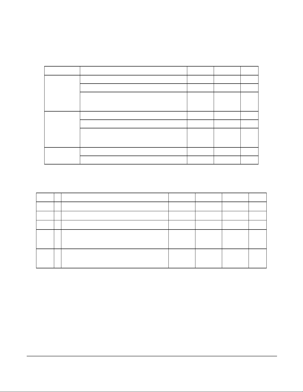
Device User Guide — 9S12DT128DGV2/D V02.16
A device will be defined as a failure if after exposure to ESD pulses the device no longer meets the device
specification. Complete DC parametric and functional testing is performed per the applicable device
specification at room temperature followed by hot temperature, unless specified otherwise in the device
specification.
Table A-2 ESD and Latch-up Test Conditions
Model Description Symbol Value Unit
Series Resistance R1 1500 Ohm
Storage Capacitance C 100 pF
Human Body
Machine
Number of Pulse per pin
positive
negative
Series Resistance R1 0 Ohm
Storage Capacitance C 200 pF
Number of Pulse per pin
positive
negative
–
–
–
3
3
–
3
3
Latch-up
Minimum input voltage limit –2.5 V
Maximum input voltage limit 7.5 V
Table A-3 ESD and Latch-Up Protection Characteristics
Num C Rating Symbol Min Max Unit
1 C Human Body Model (HBM)
2 C Machine Model (MM)
3 C Charge Device Model (CDM)
Latch-up Current at 125°C
4C
5C
positive
negative
Latch-up Current at 27°C
positive
negative
V
V
V
HBM
MM
CDM
I
LAT
I
LAT
2000 – V
200 – V
500 – V
+100
–100
+200
–200
A.1.7 Operating Conditions
–mA
–mA
This chapter describes the operating conditions of the device. Unless otherwise noted those conditions
apply to all the following data.
NOTE: Please refer to the temperature rating of the device (C, V, M) with regards to the
ambient temperature T
100
and the junction temperature TJ. For power dissipation
A
Freescale Semiconductor
 Loading...