

Quick Start Guide
S12VR64EVB
S12 MagniV Mixed-Signal MCUs
S12 MagniV
Quick Start Guide
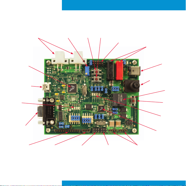
Get to Know the S12VR64EVB
LIN Connectors
Potentiometer
SW2 Analog Input
SW1
Header
External Power
Supply Banana
Connectors
JM60
Integrated
BDM
OSJTAG
Mini-B USB
Connector
GPIO
LED’s
DB9
Connector
RS-232
Comms
GPIO Header
Connector
SPI Header
Connector
LS/HS
Driver Header
Connector
Figure 1: Front Side of S12VR64EVB
Interrupt Wake
Up Input Header
Connector
Relay Motor
Output Header
Connectors
Barrel
Power
Connector
ON/OFF Switch
Relay
Reset
Switch
LS/HS
Driver LED’s
S12VR64
Microcontroller
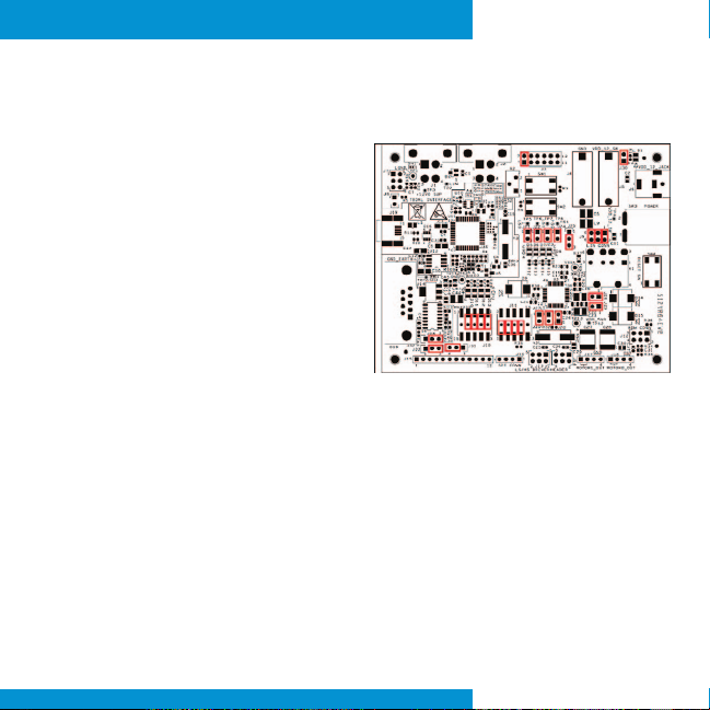
Introduction and Default Settings
The S12VR64EVB features the S12VR64,
an automotive 16-bit MCU. This family
integrates an S12 microcontroller with a
LIN physical interface, a 5-volt regulator
system to supply the microcontroller and
analog blocks to control other elements
of the system which operate at vehicle
battery level. The S12VR family uses
many of the same features found on the
S12G family, including error correction
code (ECC) on flash memory, EEPROM
for diagnostic or data storage, a fast
analog-to-digital converter (ADC) and
a frequency modulated internal phase
locked loop (IPLL) that improves the EMC
performance. This guide will show how to
quickly connect the board to a host PC
and execute a demonstration application
preloaded into flash memory. Default
jumper positions are for applications
loaded on the S12VR64EVB-board and
are shown in Figure 2.
Figure 2 - S12VR64EVB Option Settings
S12 MagniV Mixed-Signal MCUs

Quick Start Guide
Install CodeWarrior
1 2
Development Studio
The S12VR64EVB board ships with
the latest version of CodeWarrior
Development Studio for Freescale
HCS12(X) Microcontrollers. CodeWarrior
Development Studio is a complete
Integrated Development Environment
(IDE) that provides a highly visual and
automated framework to accelerate
the development of the most complex
embedded applications.
NOTE: CodeWarrior Development Studios must
be properly installed before attempting to connect
the target board to the host PC. Otherwise, the
necessary USB drivers will not be available and the
host PC will not recognize the board.
CodeWarrior Development Studio for HCS12(X) V5.1
is included on the DVD provided and can be found
on the main screen or on the software tab.
Install CodeWarrior
Service Pack for S12VR
Family Microcontrollers
Double click on the link for the S12VR
service pack. This patch contains
header files for the S12VR family
microcontrollers.
NOTE: CodeWarrior Service Pack for S12VR is
included on the DVD provided and can be found on
the main screen or on the software tab.
Launch the Demo
3
Program
The DVD contains a CodeWarrior project
to exercise the BATS module, ADC, highside drivers, the relay using low-side
drivers, Port T and SCI module. Please
follow the instructions below to compile
and load this code.
NOTE: If you want to connect a load on the relay
outputs, you’ll need to use a power supply with
a higher current output connected to the power
supply banana connectors J4 and J5.

S12 MagniV Mixed-Signal MCUs
1. Open CodeWarrior Development Studio.
2. Unzip the content of the file \files\training\
LabExamples.zip located on the training tab
of the DVD.
3. Drag the unzipped file “evb demo
application.mcp” into CodeWarrior’s Window
(the file is located below directory “evb
demo application”). This action should open
CodeWarriors’ project explorer.
4. Press “F7” key to build the project.
5. Verify the option jumpers are set in default
positions. Refer to Figure 1.
6. Connect the included A/B USB cable
between an open USB port on the host PC
and the USB connector on the target board.
7. Follow the on-screen instructions to install
the necessary USB drivers.
8. Connect a serial cable to the COM
connector at J32. Open a terminal program
and configure for 57600, 8, none, 1, none.
9. Move the ON/OFF Switch 3 to the
ON position.
10. While in CodeWarrior’s window press
“F5”; this action will attempt to establish a
connection between the evaluation board
and the PC.
11. Follow the instructions presented to connect
to the embedded debugger and download
the code recently compiled.
12. While in the debugger screen “True-Time
Simulator & Real-Time Debugger”, press
“F5” to start the code recently downloaded.
13. The relay will click on base time defined by
the potentiometer.
14. Rotate the potentiometer and notice that the
relay switching time will change according to
the potentiometer.
15. Notice that the LEDs D5, D6, D7 and D8 will
flash according to the relay changes.
16. Notice that the terminal program is reporting
the status of the system.
17. Program is reporting the status of the
VSENSE pin with an 8-bit resolution,
the current relay timer configuration on
milliseconds and the battery voltage status.
18. Vary the supply voltage below and over
the thresholds and check on the terminal
program and the battery voltage status during
this operation. (The example program is
using the VLBI2 and VHBI1 thresholds, these
thresholds are defined on the 9S12VR RM).
19. While in the Debugger window, you can halt
the controller by pressing “F6” and add break
points in the code by right clicking on it and
selecting the option “Set Break Point”.
20. Pres “F1” while in the Debugger window or
in CodeWarrior Development Studio to open
the included help.

Quick Start Guide
S12VR64EVB Jumper List and Description
Jumper Setting Description
J3 pins 1-2 closed Analog Inputs/Port AD/Keyboard Wake Up
pins 1-2 closed
J9
J10
J11
J20 closed MCU 5 Volts Output
J21 closed Low-Side Driver 0 to LED output
J22 closed Low-Side Driver 1 to LED output
pins 3-4 closed
pins 5-6 closed
pins 1-2 closed
pins 4-5 closed
pins 7-8 closed
pins 10-11 closed
pins 1-2 closed
pins 4-5 closed
pins 7-8 closed
pins 10-11 closed
Jumpers to energize the relay load. It is needed to have
all the jumpers installed
Routing of TIMER0-3, LINPHY and GPIO0 to J15 Header
Connector and LEDs D10 to D13
Routing PWM0 - ETRIG0, PWM1 - ETRIG1, HALL_SENSOR - GPIO1
and IRQ_N - GPIO2 to J15 Header Connector. Also connects
IRQ/GPIO2 to a pull up resistor.
Table 1 - Default Jumper Positions

S12 MagniV Mixed-Signal MCUs
J23 closed High-Side Driver 0 to LED output
J24 closed High-Side Driver 1 to LED output
J25 pins 2-3 closed HVI0 Input Routing
J26 closed MCU - High-Side Drivers Power Supply Pin
J27 closed 4 MHz Crystal Jumper
J28 closed 4 MHz Crystal Jumper
J29 closed VSUP and VSENSE Power supply
J30 closed Power Supply Connection LED
J31 pins 2-3 closed RS232 Transceiver Power Supply Jumper
J33 pins 2-3 closed MCU SCI TXD pin routing
J34 pins 2-3 closed MCU SCI RXD pin routing

Quick Start Guide
S12VR64EVB Jumper List and Description–continued...
Jumper Description
Analog Inputs/Port AD/Keyboard Wake Up
Analog Inputs – The jumpers are used to route the Potentiometer R2 to the ADC’s analog inputs
Jumper pins 1-2 closed - AN0 to Potentiometer R2
Jumper pins 3-4 closed - AN1 to Potentiometer R2
J3
Jumper pins 5-6 closed - AN2 to Potentiometer R2
Jumper pins 7-8 closed - AN3 to Potentiometer R2
Jumper pins 9-10 closed - AN4 to Potentiometer R2
Jumper pins 11-12 closed - AN5 to Potentiometer R2
J8 OSBDM - Jumper closed is used to enter in boot-loader mode
J9 Jumpers to energize the relay load. It is needed to have all the jumpers closed
Routing of TIMER0-3, LINPHY and GPIO0 to J15 Header Connector and LEDs D10 to D13
Jumper pin 1-2 closed routes TIMER0 GPI0 to LED D13
Jumper pin 2-3 closed routes TIMER0 GPI0 to CON_GPIO0 on Header Connector J15
Jumper pin 4-5 closed routes TIMER1 LINPHY_REG to LED D12
Jumper pin 5-6 closed routes TIMER1 LINPHY_REG to CON_LINPHY_REG on Header Connector J15
J10
Jumper pin 7-8 closed routes TIMER2 LINPHY_RXD to LED D11
Jumper pin 8-9 closed routes TIMER2 LINPHY_RXD to CON_LINPHY_RXD pin 2 on Header Connector J15
Jumper pin 10-11 closed routes TIMER3 LINPHY_TXD to LED D10
Jumper pin 11-12 closed routes TIMER3 LINPHY_TXD to CON_LINPHY_TXD pin 3 on Header Connector J15
Jumper pin 13-14-15 not connected

Jumper Description
Routing of PWM0-1, ETRIG0-1, HALL_SENSOR, GPIO0-1 and IRQ_N to Header J15.
Jumper pin 1-2 closed routes PWM0 - ETRIG0 to CON_PWM0 pin 4 on Header J15
Jumper pin 2-3 closed routes PWM0 - ETRIG0 to CON_ETRIG0 pin 6 on Header J15
Jumper pin 4-5 closed routes PWM1 - ETRIG1 to CON_PWM1 pin 5 on Header J15
J11
Jumper pin 5-6 closed routes PWM1 - ETRIG1 to CON_ETRIG1 pin 7 on Header J15
Jumper pin 7-8 closed routes HALL_SENSOR - GPIO1 to CON_HALL_SENSOR pin 8 on Header J15
Jumper pin 8-9 closed routes HALL_SENSOR - GPIO1 to CON_GPIO1 pin 11 on Header J15
Jumper pin 10-11 closed routes IRQ_N - GPIO2 to CON_IRQ_N pin 9 on Header J15 and DNP Pull up resistor
Jumper pin 11-12 closed routes IRQ_N - GPIO2 to CON_GPIO2 pin 12 on Header J15
MCU 5 Volts Output
J20
The jumper closed enables to supply the 5 Volts circuitry using the 5 Volts MCU regulated output
Low-Side Driver 0 to LED Output
J21
Closing thejumper the low-side driver is routed to LED D5
Low-Side Driver 1 to LED Output
J22
Closing the jumper the low-side driver 1 is routed to LED D6
High-Side Driver 0 to LED Output
J23
Closing the jumper the high-side driver 0 is routed to LED D7
High-Side Driver 1 to LED Output
J24
Closing the jumper the high-side driver 0 is routed to LED D8
S12 MagniV Mixed-Signal MCUs

Quick Start Guide
S12VR64EVB Jumper List and Description–continued...
Jumper Description
HVI0 Input Routing
No jumper closed - HVI0 input is floating through the R4 resistor
J25
Jumper closing 1-2 - HVI0 is routed to high-side driver 1 and if HS1 is enabled the HVI0 is pulled
up by R4 resistor
Jumper closing 2-3 - HVI0 is routed to +12V supply and it is pulled up by R4 resistor
MCU - High-Side Drivers Power Supply Pin
J26
Closing this jumper the +12V power supply source is connected to the MCU VSUPHS
4 MHz Crystal Jumper
J27
Closing the jumper the 4 MHz crystal is connected to the XTAL MCU inputs for an external oscillator
Opening the jumper the 4 MHz crystal is not connected to XTAL MCU inputs
4 MHz Crystal Jumper
J28
Closing the jumper the 4 MHz crystal is connected to the XTAL MCU inputs for an external oscillator
Opening the jumper the 4 MHz crystal is not connected to XTAL MCU inputs
VSUP and VSENSE Power Supply
J29
Closing the jumper the +12 Volts power supply is connected to the VSUP and VSENSE MCU pins
Opening the jumper the MCU is disconnected from the power supply
Power Supply Connection LED
J30
Closing this jumper allows you to have a visual indication of a power supply connected by lighting
the LED D1

Jumper Description
RS232 Transceiver Power Supply Jumper
Jumper pins 1-2 closed connects the Vcc power supply input of the RS232 transceiver to the 5V MCU
J31
regulated output
Jumper pins 2-3 closed connects the Vcc power supply input of the RS232 transceiver to the 5V RS232
voltage regulator circuitry
MCU SCI TXD Pin Routing
Jumper pins 1-2 closed connects the MCU SCI TXD pin to OSBDM SCI RXD pin for debug purposes
J33
Jumper pins 2-3 closed connects the MCU SCI TXD pin to the RS232 transceiver T1IN pin to transmitt RS232
standard data through the DB9 port
MCU SCI RXD Pin Routing
Jumper pins 1-2 closed connects the MCU SCI RXD pin to OSBDM SCI TXD pin for debug purposes
J34
Jumper pins 2-3 closed connects the MCU SCI RXD pin to the RS232 transceiver R1OUT pin to receive
RS232 standard data through the DB9 port
S12 MagniV Mixed-Signal MCUs

Quick Start Guide
S12VR64EVB Headers and Connectors List
Jumper Description
LIN Connector
1. GND
J1
2. GND
3. +12 V - LIN bus power supply
4. LIN - LIN signal
LIN Connector
1. GND
J2
2. GND
3. +12 V - LIN bus power supply
4. LIN - LIN Signal
Banana Black Connector
J4
High current power supply GND
Banana Red Connector
J5
High current power supply +12V
J6 Wall Power Supply Connector
J7 External BDM Connector for OSBDM (JM60)
J12 External BDM Connector for S12VR MCU

Jumper Description
Low-Side and High-Side Driver Header Connector
1. High-Side Driver 0
2. High-Side Driver 1
J13
3. GND
4. Low-Side Driver 1
5. Low-Side Driver 0
6. +12V Power Supply
Interrupt Wake Up Header Connector for Interrupt Wake Up 0 to Interrupt Wake Up 5
1. Interrupt Wake Up 0
2. Interrupt Wake Up 5
J14
3. Interrupt Wake Up 1
4. Interrupt Wake Up 4
5. Interrupt Wake Up 2
6. Interrupt Wake Up 3
S12 MagniV Mixed-Signal MCUs

Quick Start Guide
S12VR64EVB Headers and Connectors List–continued...
Jumper Description
Header Connector for Different Inputs and Outputs
1. CON_LINPHY_REG
2. CON_LINPHY_RXD
3. CON_LINPHY_TXD
4. CON_PWM0
5. CON_PWM1
J15
6. CON_ETRIG0
7. CON_ETRIG1
8. CON_HALL_SENSOR
9. CON_IRQ_N
10. CON_GPIO0
11. CON_GPIO1
12. CON_GPIO2
SPI Header Connector
1. CLK_SPI
J16
2. SPI_MOSI
3. SPI_MISO
4. SPI_SS

Jumper Description
J17 Supply Connector for 12V, 13A Motor Load - MOTOR1_OUT
J18 Supply Connector for 12V, 13A Motor Load - MOTOR0_OUT
J19 USB Connector for OSBMD to PC Connection
J32 DB9 Connector for Serial PC Communication
S12 MagniV Mixed-Signal MCUs

Quick Start Guide
For more information about this product,
please visit freescale.com/S12VR64EVB
Freescale, the Freescale logo and CodeWarrior are trademarks of Freescale
Semiconductor, Inc., Reg. U.S. Pat. & Tm. Off. MagniV is a trademark of
Freescale Semiconductor, Inc. All other product or service names are the
property of their respective owners.
© 2011 Freescale Semiconductor, Inc.
Doc Number: S12VR64QSG REV 3
Agile Number: 926-78584 REV D
 Loading...