

Page 1

MC9S12XHY256
Reference Manual
Covers MC9S12XHY Family
Data Sheet: Advance Information
This document contains information on a new product. Specifications and information here in are subject to change without notice.
S12
Microcontrollers
MC9S12XHY256RMV1
Rev. 1.01
03/2011
freescale.com
Downloaded from Elcodis.com electronic components distributor
Page 2

To provide the most up-to-date information, the revision of our documents on the World Wide Web will be
the most current. Your printed copy may be an earlier revision. To verify you have the latest information
available, refer to:
http://freescale.com/
A full list of family members and options is included in the appendices.
The following revision history table summarizes changes contained in this document.
This document contains information for all constituent modules, with the exception of the CPU. For CPU
information please refer to CPU12-1 in the CPU12 & CPU12X Reference Manual.
Revision History
Date
Jun,3,2010 0.11
Jun,11,2010 0.12
Mar,25,2011 1.01
Revision
Level
Description
update block: TIM SCI PIM Chapter1
update Table A-6., “5-V I/O Characteristics, item 11/12,unit is KΩ and uA
update A.1.10.1, “Typical Run Current Measurement Conditions
update Table A-6., “5-V I/O Characteristics, 4(a) , remove V C contitions
update Table A-6., “5-V I/O Characteristics,4(b), remove temperature
update Table A-10., “Run and Wait Current Characteristics, remove item
update Table A-11., “Pseudo Stop and Full Stop Current,
-10a/10b/11/12/13/14,remove temperature except -40/25/150
-15, change to FSP mode
remove Typeical Run supply table
update Table A-11., “Pseudo Stopand Full Stop Current, add LCP FSP mode
update Appendix electrical parameter
-Table A-6., “5-V I/O Characteristics 4a 9 10 11 12
Table A-11., “Pseudo Stop and Full Stop Current,10a,11a,12a,14,15
-Table A-4./A-721 LCD/Motor Driver pad can only be work under >4.5V
-A.1.3.1/A-718, change to 4.5v to 5.5v
-remove 12 bit resolution at table Table A-12./A-731
update chapter MMC to Ver04.11 3.1/3-157
update chapter MSCAN to Ver03.12
update Table D-2./D-768,all parts has 2x CAN and SCI
update Appendix electrical parameter value
Table A-11., “Pseudo Stop and Full Stop Current,
Table A-9., “Module Run Supply Currents
Table A-6., “5-V I/O Characteristics, item 4b
update Appendix, change classifications or conditions
Table A-6., “5-V I/O Characteristics, item 4b, change from 80c to 150c
Table A-11., “Pseudo Stop and Full Stop Current,item 11b,change from P to C
fix typo Table A-6., “5-V I/O Characteristics, 11 and 12, resistance not current
Downloaded from Elcodis.com electronic components distributor
Page 3

How to Reach Us:
USA/Europe/Locations not listed:
Freescale Semiconductor Literature Distribution
P.O. Box 5405, Denver, Colorado 80217
1-800-521-6274 or 480-768-2130
Japan:
Freescale Semiconductor Japan Ltd.
SPS, Technical Information Center
3-20-1, Minami-Azabu
Minato-ku
Tokyo 106-8573, Japan
81-3-3440-3569
Asia/Pacific:
Freescale Semiconductor H.K. Ltd.
2 Dai King Street
Tai Po Industrial Estate
Tai Po, N.T. Hong Kong
852-26668334
Learn More:
For more information about Freescale
Semiconductor products, please visit
http://www.freescale.com
Information in this document is provided solely to enable system and software implementers to use
Freescale Semiconductor products. There are no express or implied copyright licenses granted
hereundertodesignor fabricateany integrated circuitsor integratedcircuits basedon theinformation
in this document.
FreescaleSemiconductor reserves the right to make changes without further notice to any products
herein. Freescale Semiconductor makes no warranty, representation or guarantee regarding the
suitability of its products for any particular purpose,nor does Freescale Semiconductor assume any
liability arising out of the application or use of any product or circuit, and specifically disclaims any
andall liability,includingwithout limitation consequential or incidental damages. “Typical”parameters
which may be provided in Freescale Semiconductor data sheets and/or specifications can and do
vary in different applications and actual performance may vary over time. All operating parameters,
including “Typicals”must be validated foreach customer application by customer’stechnical experts.
FreescaleSemiconductor does not conveyanylicense under itspatent rights northe rights of others.
FreescaleSemiconductor productsare not designed,intended, or authorizedfor useas components
in systems intended for surgical implant into the body, or other applications intended to support or
sustain life, or for any other application in which the failure of the Freescale Semiconductor product
could create a situation where personal injury or death may occur. Should Buyer purchase or use
FreescaleSemiconductor products forany such unintended or unauthorized application, Buyer shall
indemnifyand hold Freescale Semiconductor and its officers,employees,subsidiaries, affiliates,and
distributors harmless against all claims, costs, damages, and expenses, and reasonable attorney
fees arising out of, directly or indirectly, any claim of personal injury or death associated with such
unintended or unauthorized use, even if such claim alleges that Freescale Semiconductor was
negligent regarding the design or manufacture of the part.
Freescale™ and the Freescale logo are trademarks of Freescale Semiconductor, Inc. All other
product or service names are the property of their respective owners.
© Freescale Semiconductor, Inc. 2006
Downloaded from Elcodis.com electronic components distributor
Page 4

MC9S12XHY-Family Reference Manual, Rev. 1.01
4 Freescale Semiconductor
Downloaded from Elcodis.com electronic components distributor
Page 5

Chapter 1
Device Overview MC9S12XHY-Family. . . . . . . . . . . . . . . . . . . . . . . . . . . . . . .13
Chapter 2
Port Integration Module (S12XHYPIMV1) . . . . . . . . . . . . . . . . . . . . . . . . . . . .65
Chapter 3
Memory Mapping Control (S12XMMCV4) . . . . . . . . . . . . . . . . . . . . . . . . . . .157
Chapter 4
Interrupt (S12XINTV2) . . . . . . . . . . . . . . . . . . . . . . . . . . . . . . . . . . . . . . . . . .181
Chapter 5
Background Debug Module (S12XBDMV2) . . . . . . . . . . . . . . . . . . . . . . . . .197
Chapter 6
S12X Debug (S12XDBGV3) Module . . . . . . . . . . . . . . . . . . . . . . . . . . . . . . . .223
Chapter 7
S12XE Clocks and Reset Generator (S12XECRGV2) . . . . . . . . . . . . . . . . .259
Chapter 8
Pierce Oscillator (S12XOSCLCPV2). . . . . . . . . . . . . . . . . . . . . . . . . . . . . . . .289
Chapter 9
Voltage Regulator (S12VREGL3V3V1). . . . . . . . . . . . . . . . . . . . . . . . . . . . . .297
Chapter 10
Analog-to-Digital Converter (ADC12B12CV1) . . . . . . . . . . . . . . . . . . . . . . .315
Chapter 11
Freescale’s Scalable Controller Area Network (S12MSCANV3) . . . . . . . . .341
Chapter 12
Inter-Integrated Circuit (IICV3) . . . . . . . . . . . . . . . . . . . . . . . . . . . . . . . . . . .395
Chapter 13
Pulse-Width Modulator (S12PWM8B8CV1) . . . . . . . . . . . . . . . . . . . . . . . . . .423
Chapter 14
Serial Communication Interface (S12SCIV5) . . . . . . . . . . . . . . . . . . . . . . . .455
Chapter 15
Serial Peripheral Interface (S12SPIV5) . . . . . . . . . . . . . . . . . . . . . . . . . . . . .493
Chapter 16
Timer Module (TIM16B8CV2) . . . . . . . . . . . . . . . . . . . . . . . . . . . . . . . . . . . . .519
MC9S12XHY-Family Reference Manual, Rev. 1.01
Freescale Semiconductor 5
Downloaded from Elcodis.com electronic components distributor
Page 6

Chapter 17
Liquid Crystal Display (LCD40F4BV2) . . . . . . . . . . . . . . . . . . . . . . . . . . . . .547
Chapter 18
256 KByte Flash Module (S12XFTMR256K1V1) . . . . . . . . . . . . . . . . . . . . . .569
Chapter 19
128 KByte Flash Module (S12XFTMR128K1V1) . . . . . . . . . . . . . . . . . . . . . .619
Chapter 20
Motor Controller (MC10B8CV1) . . . . . . . . . . . . . . . . . . . . . . . . . . . . . . . . . . .667
Chapter 21
Stepper Stall Detector (SSDV1) . . . . . . . . . . . . . . . . . . . . . . . . . . . . . . . . . . .699
Appendix A
Electrical Characteristics . . . . . . . . . . . . . . . . . . . . . . . . . . . . . . . . . . . . . . . .717
Appendix B
Package and Die Information . . . . . . . . . . . . . . . . . . . . . . . . . . . . . . . . . . . . .758
Appendix C
PCB Layout Guidelines. . . . . . . . . . . . . . . . . . . . . . . . . . . . . . . . . . . . . . . . . .765
Appendix D
Derivative Differences. . . . . . . . . . . . . . . . . . . . . . . . . . . . . . . . . . . . . . . . . . .768
Appendix E
Detailed Register Address Map . . . . . . . . . . . . . . . . . . . . . . . . . . . . . . . . . . .768
Appendix F
Ordering Information. . . . . . . . . . . . . . . . . . . . . . . . . . . . . . . . . . . . . . . . . . . .799
MC9S12XHY-Family Reference Manual, Rev. 1.01
6 Freescale Semiconductor
Downloaded from Elcodis.com electronic components distributor
Page 7

Chapter 1
Device Overview MC9S12XHY-Family
1.1 Introduction . . . . . . . . . . . . . . . . . . . . . . . . . . . . . . . . . . . . . . . . . . . . . . . . . . . . . . . . . . . . . . . . . . 13
1.2 Features . . . . . . . . . . . . . . . . . . . . . . . . . . . . . . . . . . . . . . . . . . . . . . . . . . . . . . . . . . . . . . . . . . . . . 13
1.3 Module Features . . . . . . . . . . . . . . . . . . . . . . . . . . . . . . . . . . . . . . . . . . . . . . . . . . . . . . . . . . . . . . . 15
1.4 Block Diagram . . . . . . . . . . . . . . . . . . . . . . . . . . . . . . . . . . . . . . . . . . . . . . . . . . . . . . . . . . . . . . . . 22
1.5 Device Memory Map . . . . . . . . . . . . . . . . . . . . . . . . . . . . . . . . . . . . . . . . . . . . . . . . . . . . . . . . . . . 23
1.6 Part ID Assignments . . . . . . . . . . . . . . . . . . . . . . . . . . . . . . . . . . . . . . . . . . . . . . . . . . . . . . . . . . . . 27
1.7 Signal Description . . . . . . . . . . . . . . . . . . . . . . . . . . . . . . . . . . . . . . . . . . . . . . . . . . . . . . . . . . . . . 27
1.8 System Clock Description . . . . . . . . . . . . . . . . . . . . . . . . . . . . . . . . . . . . . . . . . . . . . . . . . . . . . . . 51
1.9 Modes of Operation . . . . . . . . . . . . . . . . . . . . . . . . . . . . . . . . . . . . . . . . . . . . . . . . . . . . . . . . . . . . 52
1.10 Security . . . . . . . . . . . . . . . . . . . . . . . . . . . . . . . . . . . . . . . . . . . . . . . . . . . . . . . . . . . . . . . . . . . . . . 55
1.11 Resets and Interrupts . . . . . . . . . . . . . . . . . . . . . . . . . . . . . . . . . . . . . . . . . . . . . . . . . . . . . . . . . . . 55
1.12 COP Configuration . . . . . . . . . . . . . . . . . . . . . . . . . . . . . . . . . . . . . . . . . . . . . . . . . . . . . . . . . . . . . 59
1.13 ATD External Trigger Input Connection . . . . . . . . . . . . . . . . . . . . . . . . . . . . . . . . . . . . . . . . . . . .59
1.14 ATD Channel[17] Connection . . . . . . . . . . . . . . . . . . . . . . . . . . . . . . . . . . . . . . . . . . . . . . . . . . . . 60
1.15 VREG Configuration . . . . . . . . . . . . . . . . . . . . . . . . . . . . . . . . . . . . . . . . . . . . . . . . . . . . . . . . . . . 60
1.16 Oscillator Configuration . . . . . . . . . . . . . . . . . . . . . . . . . . . . . . . . . . . . . . . . . . . . . . . . . . . . . . . . . 61
1.17 Documentation Note . . . . . . . . . . . . . . . . . . . . . . . . . . . . . . . . . . . . . . . . . . . . . . . . . . . . . . . . . . . 62
Chapter 2
Port Integration Module (S12XHYPIMV1)
2.1 Introduction . . . . . . . . . . . . . . . . . . . . . . . . . . . . . . . . . . . . . . . . . . . . . . . . . . . . . . . . . . . . . . . . . . 66
2.2 External Signal Description . . . . . . . . . . . . . . . . . . . . . . . . . . . . . . . . . . . . . . . . . . . . . . . . . . . . . . 67
2.3 Memory Map and Register Definition . . . . . . . . . . . . . . . . . . . . . . . . . . . . . . . . . . . . . . . . . . . . . .74
2.4 Functional Description . . . . . . . . . . . . . . . . . . . . . . . . . . . . . . . . . . . . . . . . . . . . . . . . . . . . . . . . . 150
2.5 Initialization Information . . . . . . . . . . . . . . . . . . . . . . . . . . . . . . . . . . . . . . . . . . . . . . . . . . . . . . . 155
Chapter 3
Memory Mapping Control (S12XMMCV4)
3.1 Introduction . . . . . . . . . . . . . . . . . . . . . . . . . . . . . . . . . . . . . . . . . . . . . . . . . . . . . . . . . . . . . . . . . 157
3.2 External Signal Description . . . . . . . . . . . . . . . . . . . . . . . . . . . . . . . . . . . . . . . . . . . . . . . . . . . . . 160
3.3 Memory Map and Registers . . . . . . . . . . . . . . . . . . . . . . . . . . . . . . . . . . . . . . . . . . . . . . . . . . . . . 161
3.4 Functional Description . . . . . . . . . . . . . . . . . . . . . . . . . . . . . . . . . . . . . . . . . . . . . . . . . . . . . . . . . 170
3.5 Initialization/Application Information . . . . . . . . . . . . . . . . . . . . . . . . . . . . . . . . . . . . . . . . . . . . . 178
Chapter 4
Interrupt (S12XINTV2)
4.1 Introduction . . . . . . . . . . . . . . . . . . . . . . . . . . . . . . . . . . . . . . . . . . . . . . . . . . . . . . . . . . . . . . . . . 181
4.2 External Signal Description . . . . . . . . . . . . . . . . . . . . . . . . . . . . . . . . . . . . . . . . . . . . . . . . . . . . . 184
4.3 Memory Map and Register Definition . . . . . . . . . . . . . . . . . . . . . . . . . . . . . . . . . . . . . . . . . . . . . 185
4.4 Functional Description . . . . . . . . . . . . . . . . . . . . . . . . . . . . . . . . . . . . . . . . . . . . . . . . . . . . . . . . . 191
4.5 Initialization/Application Information . . . . . . . . . . . . . . . . . . . . . . . . . . . . . . . . . . . . . . . . . . . . . 195
MC9S12XHY-Family Reference Manual, Rev. 1.01
Freescale Semiconductor 7
Downloaded from Elcodis.com electronic components distributor
Page 8

Chapter 5
Background Debug Module (S12XBDMV2)
5.1 Introduction . . . . . . . . . . . . . . . . . . . . . . . . . . . . . . . . . . . . . . . . . . . . . . . . . . . . . . . . . . . . . . . . . 197
5.2 External Signal Description . . . . . . . . . . . . . . . . . . . . . . . . . . . . . . . . . . . . . . . . . . . . . . . . . . . . . 199
5.3 Memory Map and Register Definition . . . . . . . . . . . . . . . . . . . . . . . . . . . . . . . . . . . . . . . . . . . . . 200
5.4 Functional Description . . . . . . . . . . . . . . . . . . . . . . . . . . . . . . . . . . . . . . . . . . . . . . . . . . . . . . . . . 205
Chapter 6
S12X Debug (S12XDBGV3) Module
6.1 Introduction . . . . . . . . . . . . . . . . . . . . . . . . . . . . . . . . . . . . . . . . . . . . . . . . . . . . . . . . . . . . . . . . . 223
6.2 External Signal Description . . . . . . . . . . . . . . . . . . . . . . . . . . . . . . . . . . . . . . . . . . . . . . . . . . . . . 226
6.3 Memory Map and Registers . . . . . . . . . . . . . . . . . . . . . . . . . . . . . . . . . . . . . . . . . . . . . . . . . . . . . 226
6.4 Functional Description . . . . . . . . . . . . . . . . . . . . . . . . . . . . . . . . . . . . . . . . . . . . . . . . . . . . . . . . . 243
Chapter 7
S12XE Clocks and Reset Generator (S12XECRGV2)
7.1 Introduction . . . . . . . . . . . . . . . . . . . . . . . . . . . . . . . . . . . . . . . . . . . . . . . . . . . . . . . . . . . . . . . . . 259
7.2 Signal Description . . . . . . . . . . . . . . . . . . . . . . . . . . . . . . . . . . . . . . . . . . . . . . . . . . . . . . . . . . . . 261
7.3 Memory Map and Registers . . . . . . . . . . . . . . . . . . . . . . . . . . . . . . . . . . . . . . . . . . . . . . . . . . . . . 262
7.4 Functional Description . . . . . . . . . . . . . . . . . . . . . . . . . . . . . . . . . . . . . . . . . . . . . . . . . . . . . . . . . 276
7.5 Resets . . . . . . . . . . . . . . . . . . . . . . . . . . . . . . . . . . . . . . . . . . . . . . . . . . . . . . . . . . . . . . . . . . . . . . 284
7.6 Interrupts . . . . . . . . . . . . . . . . . . . . . . . . . . . . . . . . . . . . . . . . . . . . . . . . . . . . . . . . . . . . . . . . . . . 287
Chapter 8
Pierce Oscillator (S12XOSCLCPV2)
8.1 Introduction . . . . . . . . . . . . . . . . . . . . . . . . . . . . . . . . . . . . . . . . . . . . . . . . . . . . . . . . . . . . . . . . . 289
8.2 External Signal Description . . . . . . . . . . . . . . . . . . . . . . . . . . . . . . . . . . . . . . . . . . . . . . . . . . . . . 290
8.3 Memory Map and Register Definition . . . . . . . . . . . . . . . . . . . . . . . . . . . . . . . . . . . . . . . . . . . . . 292
8.4 Functional Description . . . . . . . . . . . . . . . . . . . . . . . . . . . . . . . . . . . . . . . . . . . . . . . . . . . . . . . . . 292
Chapter 9
Voltage Regulator (S12VREGL3V3V1)
9.1 Introduction . . . . . . . . . . . . . . . . . . . . . . . . . . . . . . . . . . . . . . . . . . . . . . . . . . . . . . . . . . . . . . . . . 297
9.2 External Signal Description . . . . . . . . . . . . . . . . . . . . . . . . . . . . . . . . . . . . . . . . . . . . . . . . . . . . . 300
9.3 Memory Map and Register Definition . . . . . . . . . . . . . . . . . . . . . . . . . . . . . . . . . . . . . . . . . . . . . 301
9.4 Functional Description . . . . . . . . . . . . . . . . . . . . . . . . . . . . . . . . . . . . . . . . . . . . . . . . . . . . . . . . . 310
Chapter 10
Analog-to-Digital Converter (ADC12B12CV1)
Block Description
10.1 Introduction . . . . . . . . . . . . . . . . . . . . . . . . . . . . . . . . . . . . . . . . . . . . . . . . . . . . . . . . . . . . . . . . . 315
10.2 Signal Description . . . . . . . . . . . . . . . . . . . . . . . . . . . . . . . . . . . . . . . . . . . . . . . . . . . . . . . . . . . . 319
10.3 Memory Map and Register Definition . . . . . . . . . . . . . . . . . . . . . . . . . . . . . . . . . . . . . . . . . . . . . 319
MC9S12XHY-Family Reference Manual, Rev. 1.01
8 Freescale Semiconductor
Downloaded from Elcodis.com electronic components distributor
Page 9

10.4 Functional Description . . . . . . . . . . . . . . . . . . . . . . . . . . . . . . . . . . . . . . . . . . . . . . . . . . . . . . . . . 338
10.5 Resets . . . . . . . . . . . . . . . . . . . . . . . . . . . . . . . . . . . . . . . . . . . . . . . . . . . . . . . . . . . . . . . . . . . . . . 339
10.6 Interrupts . . . . . . . . . . . . . . . . . . . . . . . . . . . . . . . . . . . . . . . . . . . . . . . . . . . . . . . . . . . . . . . . . . . 340
Chapter 11
Freescale’s Scalable Controller Area Network (S12MSCANV3)
11.1 Introduction . . . . . . . . . . . . . . . . . . . . . . . . . . . . . . . . . . . . . . . . . . . . . . . . . . . . . . . . . . . . . . . . . 341
11.2 External Signal Description . . . . . . . . . . . . . . . . . . . . . . . . . . . . . . . . . . . . . . . . . . . . . . . . . . . . . 344
11.3 Memory Map and Register Definition . . . . . . . . . . . . . . . . . . . . . . . . . . . . . . . . . . . . . . . . . . . . . 345
11.4 Functional Description . . . . . . . . . . . . . . . . . . . . . . . . . . . . . . . . . . . . . . . . . . . . . . . . . . . . . . . . . 377
11.5 Initialization/Application Information . . . . . . . . . . . . . . . . . . . . . . . . . . . . . . . . . . . . . . . . . . . . . 394
Chapter 12
Inter-Integrated Circuit (IICV3) Block Description
12.1 Introduction . . . . . . . . . . . . . . . . . . . . . . . . . . . . . . . . . . . . . . . . . . . . . . . . . . . . . . . . . . . . . . . . . 395
12.2 External Signal Description . . . . . . . . . . . . . . . . . . . . . . . . . . . . . . . . . . . . . . . . . . . . . . . . . . . . . 398
12.3 Memory Map and Register Definition . . . . . . . . . . . . . . . . . . . . . . . . . . . . . . . . . . . . . . . . . . . . . 398
12.4 Functional Description . . . . . . . . . . . . . . . . . . . . . . . . . . . . . . . . . . . . . . . . . . . . . . . . . . . . . . . . . 410
12.5 Resets . . . . . . . . . . . . . . . . . . . . . . . . . . . . . . . . . . . . . . . . . . . . . . . . . . . . . . . . . . . . . . . . . . . . . . 415
12.6 Interrupts . . . . . . . . . . . . . . . . . . . . . . . . . . . . . . . . . . . . . . . . . . . . . . . . . . . . . . . . . . . . . . . . . . . 415
12.7 Application Information . . . . . . . . . . . . . . . . . . . . . . . . . . . . . . . . . . . . . . . . . . . . . . . . . . . . . . . . 416
Chapter 13
Pulse-Width Modulator (S12PWM8B8CV1)
13.1 Introduction . . . . . . . . . . . . . . . . . . . . . . . . . . . . . . . . . . . . . . . . . . . . . . . . . . . . . . . . . . . . . . . . . 423
13.2 External Signal Description . . . . . . . . . . . . . . . . . . . . . . . . . . . . . . . . . . . . . . . . . . . . . . . . . . . . . 424
13.3 Memory Map and Register Definition . . . . . . . . . . . . . . . . . . . . . . . . . . . . . . . . . . . . . . . . . . . . . 425
13.4 Functional Description . . . . . . . . . . . . . . . . . . . . . . . . . . . . . . . . . . . . . . . . . . . . . . . . . . . . . . . . . 441
13.5 Resets . . . . . . . . . . . . . . . . . . . . . . . . . . . . . . . . . . . . . . . . . . . . . . . . . . . . . . . . . . . . . . . . . . . . . . 452
13.6 Interrupts . . . . . . . . . . . . . . . . . . . . . . . . . . . . . . . . . . . . . . . . . . . . . . . . . . . . . . . . . . . . . . . . . . . 453
Chapter 14
Serial Communication Interface (S12SCIV5)
14.1 Introduction . . . . . . . . . . . . . . . . . . . . . . . . . . . . . . . . . . . . . . . . . . . . . . . . . . . . . . . . . . . . . . . . . 455
14.2 External Signal Description . . . . . . . . . . . . . . . . . . . . . . . . . . . . . . . . . . . . . . . . . . . . . . . . . . . . . 458
14.3 Memory Map and Register Definition . . . . . . . . . . . . . . . . . . . . . . . . . . . . . . . . . . . . . . . . . . . . . 458
14.4 Functional Description . . . . . . . . . . . . . . . . . . . . . . . . . . . . . . . . . . . . . . . . . . . . . . . . . . . . . . . . . 471
14.5 Initialization/Application Information . . . . . . . . . . . . . . . . . . . . . . . . . . . . . . . . . . . . . . . . . . . . . 489
Chapter 15
Serial Peripheral Interface (S12SPIV5)
15.1 Introduction . . . . . . . . . . . . . . . . . . . . . . . . . . . . . . . . . . . . . . . . . . . . . . . . . . . . . . . . . . . . . . . . . 493
15.2 External Signal Description . . . . . . . . . . . . . . . . . . . . . . . . . . . . . . . . . . . . . . . . . . . . . . . . . . . . . 495
15.3 Memory Map and Register Definition . . . . . . . . . . . . . . . . . . . . . . . . . . . . . . . . . . . . . . . . . . . . . 496
MC9S12XHY-Family Reference Manual, Rev. 1.01
Freescale Semiconductor 9
Downloaded from Elcodis.com electronic components distributor
Page 10

15.4 Functional Description . . . . . . . . . . . . . . . . . . . . . . . . . . . . . . . . . . . . . . . . . . . . . . . . . . . . . . . . . 505
Chapter 16
Timer Module (TIM16B8CV2) Block Description
16.1 Introduction . . . . . . . . . . . . . . . . . . . . . . . . . . . . . . . . . . . . . . . . . . . . . . . . . . . . . . . . . . . . . . . . . 519
16.2 External Signal Description . . . . . . . . . . . . . . . . . . . . . . . . . . . . . . . . . . . . . . . . . . . . . . . . . . . . . 523
16.3 Memory Map and Register Definition . . . . . . . . . . . . . . . . . . . . . . . . . . . . . . . . . . . . . . . . . . . . . 524
16.4 Functional Description . . . . . . . . . . . . . . . . . . . . . . . . . . . . . . . . . . . . . . . . . . . . . . . . . . . . . . . . . 541
16.5 Resets . . . . . . . . . . . . . . . . . . . . . . . . . . . . . . . . . . . . . . . . . . . . . . . . . . . . . . . . . . . . . . . . . . . . . . 545
16.6 Interrupts . . . . . . . . . . . . . . . . . . . . . . . . . . . . . . . . . . . . . . . . . . . . . . . . . . . . . . . . . . . . . . . . . . . 545
Chapter 17
Liquid Crystal Display (LCD40F4BV2) Block Description
17.1 Introduction . . . . . . . . . . . . . . . . . . . . . . . . . . . . . . . . . . . . . . . . . . . . . . . . . . . . . . . . . . . . . . . . . 547
17.2 External Signal Description . . . . . . . . . . . . . . . . . . . . . . . . . . . . . . . . . . . . . . . . . . . . . . . . . . . . . 550
17.3 Memory Map and Register Definition . . . . . . . . . . . . . . . . . . . . . . . . . . . . . . . . . . . . . . . . . . . . . 550
17.4 Functional Description . . . . . . . . . . . . . . . . . . . . . . . . . . . . . . . . . . . . . . . . . . . . . . . . . . . . . . . . . 557
17.5 Resets . . . . . . . . . . . . . . . . . . . . . . . . . . . . . . . . . . . . . . . . . . . . . . . . . . . . . . . . . . . . . . . . . . . . . . 567
17.6 Interrupts . . . . . . . . . . . . . . . . . . . . . . . . . . . . . . . . . . . . . . . . . . . . . . . . . . . . . . . . . . . . . . . . . . . 567
Chapter 18
256 KByte Flash Module (S12XFTMR256K1V1)
18.1 Introduction . . . . . . . . . . . . . . . . . . . . . . . . . . . . . . . . . . . . . . . . . . . . . . . . . . . . . . . . . . . . . . . . . 569
18.2 External Signal Description . . . . . . . . . . . . . . . . . . . . . . . . . . . . . . . . . . . . . . . . . . . . . . . . . . . . . 572
18.3 Memory Map and Registers . . . . . . . . . . . . . . . . . . . . . . . . . . . . . . . . . . . . . . . . . . . . . . . . . . . . . 572
18.4 Functional Description . . . . . . . . . . . . . . . . . . . . . . . . . . . . . . . . . . . . . . . . . . . . . . . . . . . . . . . . . 596
18.5 Security . . . . . . . . . . . . . . . . . . . . . . . . . . . . . . . . . . . . . . . . . . . . . . . . . . . . . . . . . . . . . . . . . . . . . 615
18.6 Initialization . . . . . . . . . . . . . . . . . . . . . . . . . . . . . . . . . . . . . . . . . . . . . . . . . . . . . . . . . . . . . . . . . 617
Chapter 19
128 KByte Flash Module (S12XFTMR128K1V1)
19.1 Introduction . . . . . . . . . . . . . . . . . . . . . . . . . . . . . . . . . . . . . . . . . . . . . . . . . . . . . . . . . . . . . . . . . 619
19.2 Memory Map and Registers . . . . . . . . . . . . . . . . . . . . . . . . . . . . . . . . . . . . . . . . . . . . . . . . . . . . . 621
19.3 Functional Description . . . . . . . . . . . . . . . . . . . . . . . . . . . . . . . . . . . . . . . . . . . . . . . . . . . . . . . . . 645
19.4 Security . . . . . . . . . . . . . . . . . . . . . . . . . . . . . . . . . . . . . . . . . . . . . . . . . . . . . . . . . . . . . . . . . . . . . 664
19.5 Initialization . . . . . . . . . . . . . . . . . . . . . . . . . . . . . . . . . . . . . . . . . . . . . . . . . . . . . . . . . . . . . . . . . 666
Chapter 20
Motor Controller (MC10B8CV1)
20.1 Introduction . . . . . . . . . . . . . . . . . . . . . . . . . . . . . . . . . . . . . . . . . . . . . . . . . . . . . . . . . . . . . . . . . 667
20.2 External Signal Description . . . . . . . . . . . . . . . . . . . . . . . . . . . . . . . . . . . . . . . . . . . . . . . . . . . . . 670
20.3 Memory Map and Register Definition . . . . . . . . . . . . . . . . . . . . . . . . . . . . . . . . . . . . . . . . . . . . . 671
20.4 Functional Description . . . . . . . . . . . . . . . . . . . . . . . . . . . . . . . . . . . . . . . . . . . . . . . . . . . . . . . . . 679
20.5 Reset . . . . . . . . . . . . . . . . . . . . . . . . . . . . . . . . . . . . . . . . . . . . . . . . . . . . . . . . . . . . . . . . . . . . . . . 693
MC9S12XHY-Family Reference Manual, Rev. 1.01
10 Freescale Semiconductor
Downloaded from Elcodis.com electronic components distributor
Page 11

20.6 Interrupts . . . . . . . . . . . . . . . . . . . . . . . . . . . . . . . . . . . . . . . . . . . . . . . . . . . . . . . . . . . . . . . . . . . 693
20.7 Initialization/Application Information . . . . . . . . . . . . . . . . . . . . . . . . . . . . . . . . . . . . . . . . . . . . . 694
Chapter 21
Stepper Stall Detector (SSDV1) Block Description
21.1 Introduction . . . . . . . . . . . . . . . . . . . . . . . . . . . . . . . . . . . . . . . . . . . . . . . . . . . . . . . . . . . . . . . . . 699
21.2 External Signal Description . . . . . . . . . . . . . . . . . . . . . . . . . . . . . . . . . . . . . . . . . . . . . . . . . . . . . 701
21.3 Memory Map and Register Definition . . . . . . . . . . . . . . . . . . . . . . . . . . . . . . . . . . . . . . . . . . . . . 702
21.4 Functional Description . . . . . . . . . . . . . . . . . . . . . . . . . . . . . . . . . . . . . . . . . . . . . . . . . . . . . . . . . 710
Appendix A
Electrical Characteristics
A.1 General . . . . . . . . . . . . . . . . . . . . . . . . . . . . . . . . . . . . . . . . . . . . . . . . . . . . . . . . . . . . . . . . . . . . . 717
A.1.1 Parameter Classification . . . . . . . . . . . . . . . . . . . . . . . . . . . . . . . . . . . . . . . . . . . . . . . . . 717
A.1.2 Power Supply . . . . . . . . . . . . . . . . . . . . . . . . . . . . . . . . . . . . . . . . . . . . . . . . . . . . . . . . . 717
A.1.3 Pins . . . . . . . . . . . . . . . . . . . . . . . . . . . . . . . . . . . . . . . . . . . . . . . . . . . . . . . . . . . . . . . . . 718
A.1.4 Current Injection. . . . . . . . . . . . . . . . . . . . . . . . . . . . . . . . . . . . . . . . . . . . . . . . . . . . . . . 719
A.1.5 Absolute Maximum Ratings. . . . . . . . . . . . . . . . . . . . . . . . . . . . . . . . . . . . . . . . . . . . . . 719
A.1.6 ESD Protection and Latch-up Immunity. . . . . . . . . . . . . . . . . . . . . . . . . . . . . . . . . . . . . 720
A.1.7 Operating Conditions . . . . . . . . . . . . . . . . . . . . . . . . . . . . . . . . . . . . . . . . . . . . . . . . . . . 721
A.1.8 Power Dissipation and Thermal Characteristics. . . . . . . . . . . . . . . . . . . . . . . . . . . . . . . 722
A.1.9 I/O Characteristics . . . . . . . . . . . . . . . . . . . . . . . . . . . . . . . . . . . . . . . . . . . . . . . . . . . . . 724
A.1.10 Supply Currents . . . . . . . . . . . . . . . . . . . . . . . . . . . . . . . . . . . . . . . . . . . . . . . . . . . . . . . 726
A.2 ATD Characteristics . . . . . . . . . . . . . . . . . . . . . . . . . . . . . . . . . . . . . . . . . . . . . . . . . . . . . . . . . . . 731
A.2.1 ATD Operating Characteristics. . . . . . . . . . . . . . . . . . . . . . . . . . . . . . . . . . . . . . . . . . . . 731
A.2.2 Factors Influencing Accuracy. . . . . . . . . . . . . . . . . . . . . . . . . . . . . . . . . . . . . . . . . . . . . 731
A.2.3 ATD Accuracy . . . . . . . . . . . . . . . . . . . . . . . . . . . . . . . . . . . . . . . . . . . . . . . . . . . . . . . . 733
A.3 NVM, Flash. . . . . . . . . . . . . . . . . . . . . . . . . . . . . . . . . . . . . . . . . . . . . . . . . . . . . . . . . . . . . . . . . . 736
A.3.1 Timing Parameters . . . . . . . . . . . . . . . . . . . . . . . . . . . . . . . . . . . . . . . . . . . . . . . . . . . . . 736
A.3.2 NVM Reliability Parameters. . . . . . . . . . . . . . . . . . . . . . . . . . . . . . . . . . . . . . . . . . . . . . 741
A.4 Voltage Regulator . . . . . . . . . . . . . . . . . . . . . . . . . . . . . . . . . . . . . . . . . . . . . . . . . . . . . . . . . . . . . 743
A.5 Output Loads. . . . . . . . . . . . . . . . . . . . . . . . . . . . . . . . . . . . . . . . . . . . . . . . . . . . . . . . . . . . . . . . . 744
A.5.1 Resistive Loads. . . . . . . . . . . . . . . . . . . . . . . . . . . . . . . . . . . . . . . . . . . . . . . . . . . . . . . . 744
A.5.2 Capacitive Loads. . . . . . . . . . . . . . . . . . . . . . . . . . . . . . . . . . . . . . . . . . . . . . . . . . . . . . . 744
A.5.3 Chip Power-up and Voltage Drops. . . . . . . . . . . . . . . . . . . . . . . . . . . . . . . . . . . . . . . . . 744
A.6 Reset, Oscillator and PLL . . . . . . . . . . . . . . . . . . . . . . . . . . . . . . . . . . . . . . . . . . . . . . . . . . . . . . . 746
A.6.1 Startup. . . . . . . . . . . . . . . . . . . . . . . . . . . . . . . . . . . . . . . . . . . . . . . . . . . . . . . . . . . . . . . 746
A.6.2 Oscillator. . . . . . . . . . . . . . . . . . . . . . . . . . . . . . . . . . . . . . . . . . . . . . . . . . . . . . . . . . . . . 748
A.6.3 Phase Locked Loop. . . . . . . . . . . . . . . . . . . . . . . . . . . . . . . . . . . . . . . . . . . . . . . . . . . . . 748
A.7 LCD Driver . . . . . . . . . . . . . . . . . . . . . . . . . . . . . . . . . . . . . . . . . . . . . . . . . . . . . . . . . . . . . . . . . . 750
A.8 MSCAN. . . . . . . . . . . . . . . . . . . . . . . . . . . . . . . . . . . . . . . . . . . . . . . . . . . . . . . . . . . . . . . . . . . . . 753
A.9 SPI Timing . . . . . . . . . . . . . . . . . . . . . . . . . . . . . . . . . . . . . . . . . . . . . . . . . . . . . . . . . . . . . . . . . . 754
A.9.1 Master Mode. . . . . . . . . . . . . . . . . . . . . . . . . . . . . . . . . . . . . . . . . . . . . . . . . . . . . . . . . . 754
A.9.2 Slave Mode . . . . . . . . . . . . . . . . . . . . . . . . . . . . . . . . . . . . . . . . . . . . . . . . . . . . . . . . . . . 756
MC9S12XHY-Family Reference Manual, Rev. 1.01
Freescale Semiconductor 11
Downloaded from Elcodis.com electronic components distributor
Page 12

Appendix B
Package and Die Information
B.1 112-pin LQFP Mechanical Dimensions . . . . . . . . . . . . . . . . . . . . . . . . . . . . . . . . . . . . . . . . . . . . 759
B.2 100-Pin LQFP Mechanical Dimensions . . . . . . . . . . . . . . . . . . . . . . . . . . . . . . . . . . . . . . . . . . . . 762
Appendix C
PCB Layout Guidelines
C.1 General . . . . . . . . . . . . . . . . . . . . . . . . . . . . . . . . . . . . . . . . . . . . . . . . . . . . . . . . . . . . . . . . . . . . . 765
C.1.1 112-Pin LQFP Recommended PCB Layout . . . . . . . . . . . . . . . . . . . . . . . . . . . . . . . . . . 766
C.1.2 100-Pin QFP Recommended PCB Layout . . . . . . . . . . . . . . . . . . . . . . . . . . . . . . . . . . . 767
Appendix D
Derivative Differences
D.1 Memory Sizes and Package Options 9S12XHY family . . . . . . . . . . . . . . . . . . . . . . . . . . . . . . . . 768
Appendix E
Detailed Register Address Map
E.1 Detailed Register Map. . . . . . . . . . . . . . . . . . . . . . . . . . . . . . . . . . . . . . . . . . . . . . . . . . . . . . . . . . 768
Appendix F
Ordering Information
F.1 Ordering Information . . . . . . . . . . . . . . . . . . . . . . . . . . . . . . . . . . . . . . . . . . . . . . . . . . . . . . . . . . 799
MC9S12XHY-Family Reference Manual, Rev. 1.01
12 Freescale Semiconductor
Downloaded from Elcodis.com electronic components distributor
Page 13

Chapter 1
Device Overview MC9S12XHY-Family
1.1 Introduction
The MC9S12XHY family is an optimized, automotive, 16-bit microcontroller product line that is
specifically designed for entry level instrument clusters. This family also services generic automotive
applications requiring CAN, LCD, Motor driver control or LIN/SAE J2602. Typical examples of these
applications include instrument clusters for automobiles and 2 or 3 wheelers, HVAC displays, general
purpose motor control and body controllers.
The MC9S12XHY family uses many of the same features found on the MC9S12XS family and
MC9S12HY/HA family, including error correction code (ECC) on flash memory, a separate data-flash
module for diagnostic or data storage, a fast analog-to-digital converter (ATD) and a frequency modulated
phase locked loop (IPLL) that improves the EMC performance. The MC9S12XHY family features a 40x4
liquid crystal display (LCD) controller/driver and a motor pulse width modulator (MC) consisting of up to
16 high current outputs. The device is capable of stepper motor stall detection (SSD) via hardware or
software, please contact Freescale sales office for detailed information on software SSD.
The MC9S12XHY family deliver all the advantages and efficiencies of a 16-bit MCU while retaining the
low cost, power consumption, EMC, and code-size efficiency advantages currently enjoyed by users of
Freescale’s existing 8-bit and 16-bit MCU families. Like the MC9S12HY/HA family, the MC9S12XHY
family run 16-bit wide accesses without wait states for all peripherals and memories. The MC9S12XHY
family is available in 112-pin LQFP and 100-pin LQFP package options. In addition to the I/O ports
available in each module, further I/O ports are available with interrupt capability allowing wake-up from
stop or wait modes.
1.2 Features
This section describes the key features of the MC9S12XHY family.
MC9S12XHY-Family Reference Manual, Rev. 1.01
Freescale Semiconductor 13
Downloaded from Elcodis.com electronic components distributor
Page 14

Device Overview MC9S12XHY-Family
1.2.1 MC9S12XHY Family Comparison
Table 1-1 provides a summary of different members of the MC9S12XHY family and their proposed
features. This information is intended to provide an understanding of the range of functionality offered by
this microcontroller family.
Table 1-1. MC9S12XHY Family
Feature
CPU
Flash memory
(ECC)
Data flash (ECC)
RAM
Pin Quantity
CAN
SCI
SPI
IIC
Timer 0
Timer 1
PWM
ADC (10-bit)
Stepper Motor
Controller
MC9S12XHY128 MC9S12XHY256
HCS12X V1
128Kbytes 256 Kbytes
8 Kbytes
8 Kbytes 12kbyte
100 112 100 112
2
2
1
1
8 ch x 16-bit
8 ch x 16-bit
8 ch x 8-bit or 4ch x16-bit
8 ch 12ch 8ch 12 ch
4
Stepper Stall
Detecter
LCD Driver
(FPxBP)
Key Wakeup Pins
Frequency Modulated PLL
External osc
(4–16 MHz Pierce
with loop control)
14 Freescale Semiconductor
38x4 40x4 38x4 40x4
23 25 23 25
MC9S12XHY-Family Reference Manual, Rev. 1.01
4
Yes
Yes
Downloaded from Elcodis.com electronic components distributor
Page 15

Table 1-1. MC9S12XHY Family
Device Overview MC9S12XHY-Family
Feature
Internal 1 MHz RC
osc
Supply voltage
RTI, LVI, CRG,
RST, COP, DBG,
POR, API
Execution speed
MC9S12XHY128 MC9S12XHY256
No
4.5 V – 5.5 V
Yes
Static-40MHz
1.2.2 Chip-Level Features
On-chip modules available within the family include the following features:
• CPU12XV1 CPU core
• Up to 256 Kbyte on-chip flash with ECC
• 8Kbyte data flash with ECC
• Up to 12Kbyte on-chip SRAM
• Phase locked loop (IPLL) frequency multiplier with internal filter
• 4–16 MHz amplitude controlled Pierce oscillator
• Two timer modules (TIM0 and TIM1) supporting input/output channels that provide a range of 16bit input capture, output compare, counter and pulse accumulator functions
• Pulse width modulation (PWM) module with up to 8 x 8-bit channels
• Up to 12-channel, 10-bit resolution successive approximation analog-to-digital converter (ATD)
• Up to 40x4 LCD driver
• PWM motor controller (MC) with up to 16 high current drivers
• Output slew rate control on Motor driver pad
• One serial peripheral interface (SPI) module
• One Inter-IC bus interface (IIC) module
• Two serial communication interface (SCI) module supporting LIN communications
• Two multi-scalable controller area network (MSCAN) module (supporting CAN protocol 2.0A/B)
• On-chip voltage regulator (VREG) for regulation of input supply and all internal voltages
• Autonomous periodic interrupt (API)
• Stepper Motor Controller with up to drivers for up to 4 motors
• Four Stepper Stall Detector modules (one for each motor)
• Up to 25 key wakup inputs
1.3 Module Features
The following sections provide more details of the modules implemented on the MC9S12XHY family.
MC9S12XHY-Family Reference Manual, Rev. 1.01
Freescale Semiconductor 15
Downloaded from Elcodis.com electronic components distributor
Page 16

Device Overview MC9S12XHY-Family
1.3.1 S12 16-Bit Central Processor Unit (CPU)
The CPU12X is a high-speed, 16-bit processing unit that has a programming model identical to that of the
industry standard M68HC11 central processor unit (CPU).
• Upward compatible with S12 instruction set, with the exception of five Fuzzy instructions (MEM,
WAV, WAVR, REV, REVW) which have been removed
• Enhanced indexed addressing
• Access to large data segments independent of PPAGE
1.3.2 On-Chip Flash with ECC
On-chip flash memory on the MC9S12XHY features the following:
• Up to 256Kbyte of program flash memory
— 64data bits plus 8 syndrome ECC (error correction code) bits allow single bit error correction
and double fault bit detection
— Erase sector size 1024bytes
— Automated program and erase algorithm
— Protection scheme to prevent accidental program or erase
— Security option to prevent unauthorized access
— Sense-amp margin level setting for reads
• 8Kbyte data flash space
— 16 data bits plus 6 syndrome ECC (error correction code) bits allow single bit error correction
and double fault detection
— Erase sector size 256 bytes
— Automated program and erase algorithm
—
1.3.3 On-Chip SRAM
• Up to 12Kbytes of general-purpose RAM
1.3.4 Main External Oscillator (XOSC)
• Loop control Pierce oscillator using a 4 MHz to 16 MHz crystal
— Current gain control on amplitude output
— Signal with low harmonic distortion
— Low power
— Good noise immunity
— Eliminates need for external current limiting resistor
— Transconductance sized for optimum start-up margin for typical crystals
MC9S12XHY-Family Reference Manual, Rev. 1.01
16 Freescale Semiconductor
Downloaded from Elcodis.com electronic components distributor
Page 17

1.3.5 Internal Phase-Locked Loop (IPLL)
• Phase-locked-loop clock frequency multiplier
— No external components required
— Reference divider and multiplier allow large variety of clock rates
— Automatic bandwidth control mode for low-jitter operation
— Automatic frequency lock detector
— Configurable option to spread spectrum for reduced EMC radiation (frequency modulation)
–
1.3.6 Clocks and reset generation(CRG)
• COP watchdog
• Real time interrupt
• Clock monitor
• Fast wake up from STOP in self clock mode
1.3.7 System Integrity Support
Device Overview MC9S12XHY-Family
• Power-on reset (POR)
• System reset generation
• Illegal address detection with reset
• Low-voltage detection with interrupt or reset
• Real time interrupt (RTI)
• Computer operating properly (COP) watchdog
— Configurable as window COP for enhanced failure detection
— Initialized out of reset using option bits located in flash memory
• Clock monitor supervising the correct function of the oscillator
• Temperature sensor
1.3.8 Timer (TIM0)
• 8x 16-bit channels for input capture
• 8x 16-bit channels for output compare
• 16-bit free-running counter with 8-bit precision prescaler
• 1 x 16-bit pulse accumulator
1.3.9 Timer (TIM1)
• 8x 16-bit channels for input capture
• 8x 16-bit channels for output compare
MC9S12XHY-Family Reference Manual, Rev. 1.01
Freescale Semiconductor 17
Downloaded from Elcodis.com electronic components distributor
Page 18

Device Overview MC9S12XHY-Family
• 16-bit free-running counter with 8-bit precision prescaler
• 1 x 16-bit pulse accumulator
1.3.10 Liquid crystal display driver (LCD)
• Configurable for up to 40 frontplanes and 4 backplanes or general-purpose input or output
• 5 modes of operation allow for different display sizes to meet application requirements
• Unused frontplane and backplane pins can be used as general-purpose I/O
1.3.11 Motor Controller (MC)
• PWM motor controller (MC) with up to 16 high current drivers
• Each PWM channel switchable between two drivers in an H-bridge configuration
• Left, right and center aligned outputs
• Support for sine and cosine drive
• Dithering
• Output slew rate control
1.3.12 Pulse Width Modulation Module (PWM)
• 8channel x 8-bit or 4channel x 16-bit pulse width modulator
— Programmable period and duty cycle per channel
— Center-aligned or left-aligned outputs
— Programmable clock select logic with a wide range of frequencies
1.3.13 Inter-IC bus Module (IIC)
• 1 Inter-IC (IIC) bus module which has following feature
— Multi-master operation
— Soft programming for one of 256 different serial clock frequencies
— General Call(Broadcast) mode support
— 10-bit address support
1.3.14 Controller Area Network Module (MSCAN)
• 1 Mbit per second, CAN 2.0 A, B software compatible
— Standard and extended data frames
— 0–8 bytes data length
— Programmable bit rate up to 1 Mbps
• Five receive buffers with FIFO storage scheme
• Three transmit buffers with internal prioritization
• Flexible identifier acceptance filter programmable as:
MC9S12XHY-Family Reference Manual, Rev. 1.01
18 Freescale Semiconductor
Downloaded from Elcodis.com electronic components distributor
Page 19

Device Overview MC9S12XHY-Family
— 2 x 32-bit
— 4 x 16-bit
— 8 x 8-bit
• Wakeup with integrated low pass filter option
• Loop back for self test
• Listen-only mode to monitor CAN bus
• Bus-off recovery by software intervention or automatically
• 16-bit time stamp of transmitted/received messages
1.3.15 Serial Communication Interface Module (SCI)
• Full-duplex or single-wire operation
• Standard mark/space non-return-to-zero (NRZ) format
• Selectable IrDA 1.4 return-to-zero-inverted (RZI) format with programmable pulse widths
• 13-bit baud rate selection
• Programmable character length
• Programmable polarity for transmitter and receiver
• Active edge receive wakeup
• Break detect and transmit collision detect supporting LIN
1.3.16 Serial Peripheral Interface Module (SPI)
• Configurable 8- or 16-bit data size
• Full-duplex or single-wire bidirectional
• Double-buffered transmit and receive
• Master or slave mode
• MSB-first or LSB-first shifting
• Serial clock phase and polarity options
1.3.17 Analog-to-Digital Converter Module (ATD)
• Up to 12-channel, 10-bit analog-to-digital converter
— 3 us single conversion time
— 8-/10 bit resolution
— Left or right justified result data
— Internal oscillator for conversion in stop modes
— Wakeup from low power modes on analog comparison > or <= match
— Continuous conversion mode
— Multiple channel scans
• Pins can also be used as digital I/O
MC9S12XHY-Family Reference Manual, Rev. 1.01
Freescale Semiconductor 19
Downloaded from Elcodis.com electronic components distributor
Page 20

Device Overview MC9S12XHY-Family
1.3.18 On-Chip Voltage Regulator (VREG)
• Linear voltage regulator with bandgap reference
• Low-voltage detect (LVD) with low-voltage interrupt (LVI)
• Power-on reset (POR) circuit
• Low-voltage reset (LVR)
1.3.19 Background Debug (BDM)
• Background debug module (BDM) with single-wire interface
• Non-intrusive memory access commands
• Supports in-circuit programming of on-chip nonvolatile memory
1.3.20 Debugger (DBG)
• Three comparators A, B, C, and D to monitor CPU buses
• Trace buffer with depth of 64 entries
• Comparator A and C compares full address bus and 16-bit data bus with mask register
• Three modes: simple address/data match, inside address range, or outside address range
1.3.21 SSD
• Programmable Full Step State
• Programmable Integration polarity
• Blanking (recirculation) state
• 16-bit Integration Accumulator register
• 16-Bit Modulus Down Counter with interrupt
• Multiplex two stepper motors
1.3.22 INT (interrupt module)
• Seven levels of nested interrupts
• Flexible assignment of interrupt sources to each interrupt level.
• External non-maskable high priority interrupt (XIRQ)
• The following inputs can act as Wake-up Interrupts
— IRQ and non-maskable XIRQ
— CAN receive pins
— SCI receive pins
— Depending on the package option up to 25 pins on ports R, S, T and AD, configurable as rising
or falling edge sensitive
•
MC9S12XHY-Family Reference Manual, Rev. 1.01
20 Freescale Semiconductor
Downloaded from Elcodis.com electronic components distributor
Page 21

Device Overview MC9S12XHY-Family
MC9S12XHY-Family Reference Manual, Rev. 1.01
Freescale Semiconductor 21
Downloaded from Elcodis.com electronic components distributor
Page 22
Device Overview MC9S12XHY-Family
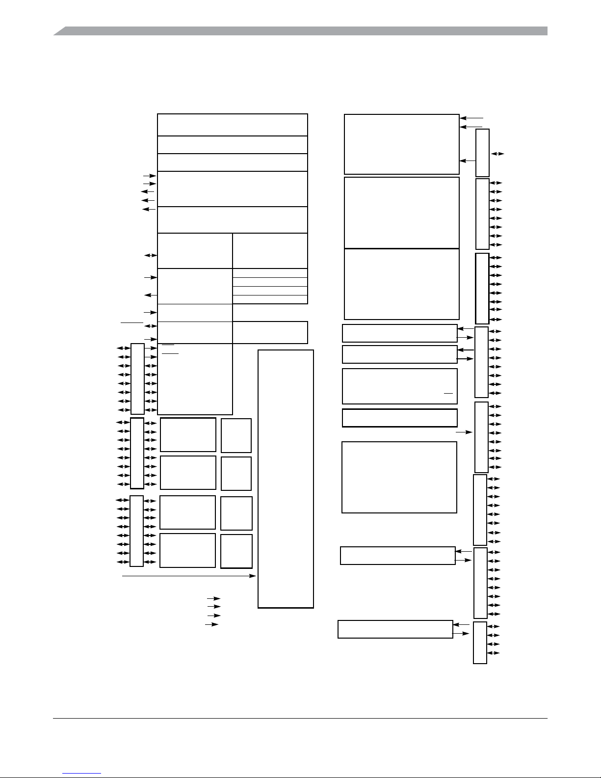
1.4 Block Diagram
Figure 1-1 shows a block diagram of the MC9S12XHY-Family devices
PA 0
PA 1
PA 2
PA 3
PA 4
PA 5
PA 6
PA 7
PU0
PU1
PU2
PU3
PU4
PU5
PU6
PU7
PV0
PV1
PV2
PV3
PV4
PV5
PV6
PV7
VLCD
VDDR
VSS3
VDD
VDDF
VDDPLL
BKGD
EXTAL
XTAL
VSSPLL
RESET
TEST
Single-wire Background
Debug Module
Amplitude Controlled
Low Power Pierce or
Full drive Pierce
Oscillator
PLL with Frequency
Modulation option
Reset Generation
and Test Entry
IRQ
XIRQ
PTA
Motor Driver0
PTU
Motor Driver1
Motor Driver2
PTV
Motor Driver3
5V IO Supply
VDDX/VSSX
VDDM1/VSSM1
VDDM2/VSSM2
VDDA/VSSA
256K/128K bytes Flash
12K/8K bytes RAM
8K bytes Data Flash
Voltage Regulator
CPU12X-V1
Debug Module
3 address breakpoints
1 data breakpoints
64 Byte Trace Buffer
Clock Monitor
COP Watchdog
Periodic Interrupt
Auto. Periodic Int.
Multilevel
Interrupt Module
SSD 0
SSD 1
SSD 2
SSD 3
ATD
10-bit 12-channel
Analog-Digital Converter
TIM1
TIM0
SCI0
Asynchronous Serial IF
CAN0
msCAN 2.0B
SPI
Synchronous Serial IF
IIC
PWM
8-bit 8channel
Pulse Width Modulator
40 X 4 LCD display
CAN1
msCAN 2.0B
SCI1
Asynchronous Serial IF
AN[7:0]
IOC1_0
IOC1_1
IOC1_2
IOC1_3
IOC1_4
IOC1_5
IOC1_6
IOC1_7
IOC0_0
IOC0_1
IOC0_2
IOC0_3
IOC0_4
IOC0_5
IOC0_6
IOC0_7
RXD
TXD
RXCAN
TXCAN
MISO
MOSI
SCK
SDA
SCL
ECLK
PWM0
PWM1
PWM2
PWM3
PWM4
PWM5
PWM6
PWM7
RXCAN
TXCAN
RXD
TXD
SS
VDDA/VRH
VSSA/VRL
PAD[11:0]
PTAD(KWU)
PT0
PT1
PT2
PT3
PT4
PT5
PTT(KWU)
PT6
PT7
PP0
PP1
PP2
PP3
PP4
PTP
PP5
PP6
PP7
PS0
PS1
PS2
PS3
PS4
PS5
PTS(KWU)
PS6
PS7
PH0
PH1
PH2
PH3
PH4
PTH
PH5
PH6
PH7
PB0
PB1
PB2
PB3
PB4
PTB
PB5
PB6
PB7
PR0
PR1
PR2
PR3
PR4
PR5
PTR(KWU)
PR6
PR7
PM0
PM1
PM2
PTM
PM3
Figure 1-1. MC9S12XHY-Family 112 LQFP Block Diagram
MC9S12XHY-Family Reference Manual, Rev. 1.01
22 Freescale Semiconductor
Downloaded from Elcodis.com electronic components distributor
Page 23

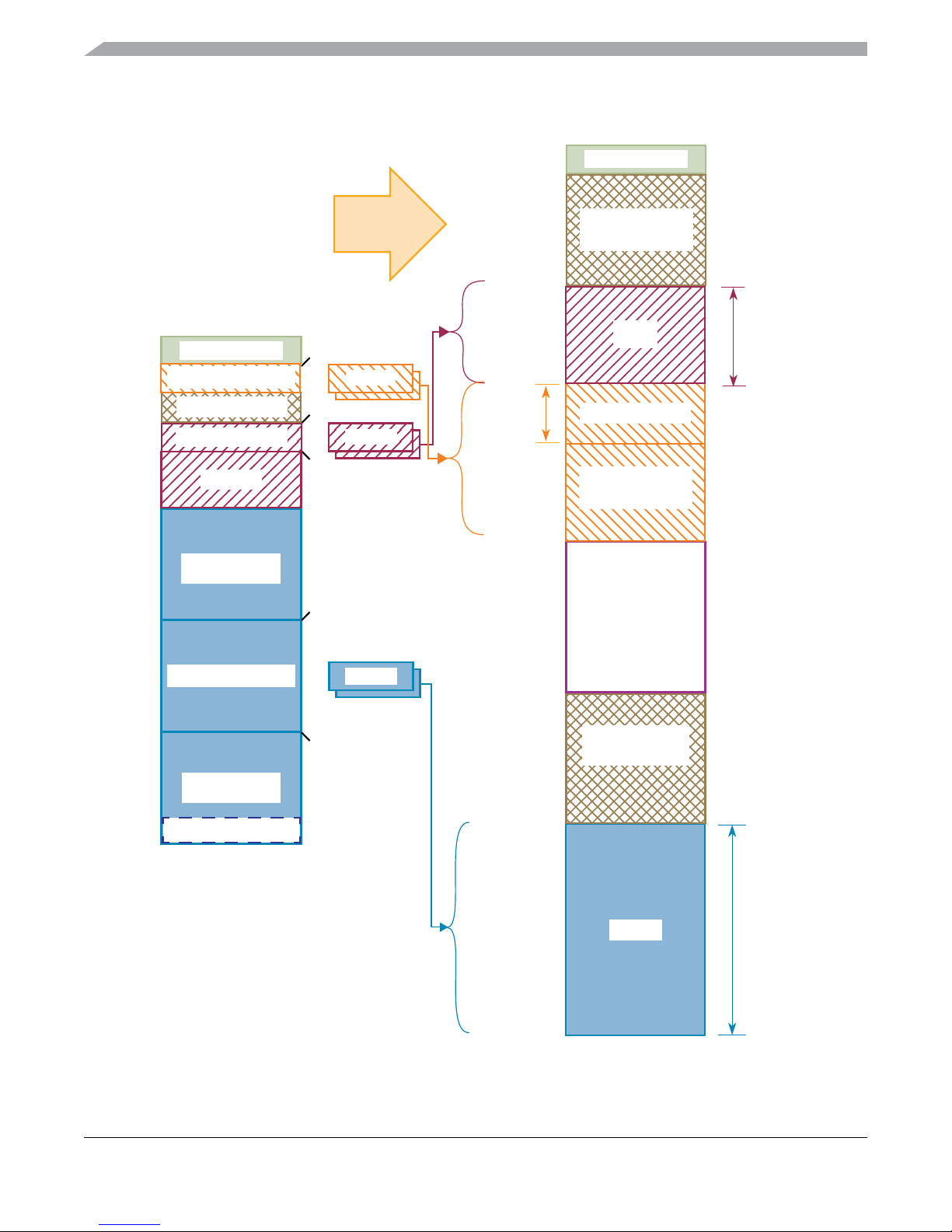
1.5 Device Memory Map
Table 1-2 shows the device register memory map.
Table 1-2. Device Register Memory Map
Device Overview MC9S12XHY-Family
Address Module
0x0000–0x0009 PIM (port integration module
0x000A–0x000B MMC (memory map control) 2 769
0x000C–0x000D PIM (port integration module) 2 769
0x000E–0x000F Reserved 2
0x0010–0x0017 MMC (memory map control) 8 769
0x0018–0x0019 Reserved 2
0x001A–0x001B Device ID register 2 770
0x001C–0x001F PIM (port integration module) 4 770
0x0020–0x002F DBG (debug module) 16 771
0x0030–0x0033 Reserved 4
0x0034–0x003F ECRG (clock and reset generator) 12 772
0x0040–0x006F TIM0 (timer module) 48 773
0x0070–0x009F ATD (analog-to-digital converter 10 bit 8-channel) 48 775
0x00A0–0x00C7 PWM (pulse-width modulator 8 channels) 40 776
0x00C8–0x00CF SCI0 (serial communications interface) 8 778
) 10 768
Size
(Bytes)
reference
pages
0x00D0–0x00D7 SCI1 (serial communications interface) 8 779
0x00D8–0x00DF SPI (serial peripheral interface) 8 779
0x00E0–0x00E7 IIC (Inter IC bus) 8 780
0x00E8–0x00FF Reserved 24
0x0100–0x0113 FTMR control registers 20 781
0x0114–0x011F Reserved 12
0x0120-0x012F INT (interrupt module) 16 782
0x0130–0x013F Reserved 16
0x0140–0x017F CAN0 64 783
0x0180–0x01BF CAN1 64 785
0x1C0–0x1FF MC(motor controller) 64 786
0x0200–0x021F LCD 32 788
0x0220–0x0227 Stepper Stall Detector 0 (SSD0) 8 789
0x0228–0x022F Stepper Stall Detector 1 (SSD1) 8 790
0x0230–0x0237 Stepper Stall Detector 2 (SSD2) 8 790
0x0238–0x023F Stepper Stall Detector 3 (SSD3) 8 791
MC9S12XHY-Family Reference Manual, Rev. 1.01
Freescale Semiconductor 23
Downloaded from Elcodis.com electronic components distributor
Page 24

Device Overview MC9S12XHY-Family
Address Module
0x0240–0x029F PIM (port integration module) 96 791
0x02A0–0x02CF TIM1(timer module) 48 795
0x02D0–0x02EF Reserved 32
0x02F0–0x02F7
0x02F8–0x02FF Reserved 8
0x0300–0x03FF Reserved 256
0x0400–0x07FF Reserved 1024
Voltage regulator
Size
(Bytes)
8 797
reference
pages
NOTE
Reserved register space shown in Table 1-2 is not allocated to any module.
This register space is reserved for future use. Writing to these locations have
no effect. Read access to these locations returns zero.
Figure 1-2 shows MC9S12XHY family CPU and BDM local address translation to the global memory
map. It indicates also the location of the internal resources in the memory map.
Accessing the reserved area in the range of 0x0C00 to 0x0FFF will return undefined data values.
A CPU access to any unimplemented space causes an illegal address reset.
The range between 0x10_0000 and 0x13_FFFF is mapped to DFLASH (Data Flash). The DFLASH block
sizes are listed in Table 1-3.
MC9S12XHY-Family Reference Manual, Rev. 1.01
24 Freescale Semiconductor
Downloaded from Elcodis.com electronic components distributor
Page 25

Device Overview MC9S12XHY-Family
Table 1-3. Derivative Dependent Memory Parameters of Device Internal Resources
Device FLASH_LOW
SIZE/
PPAGE
(1)
RAM_LOW
SIZE/
RPAGE
(2)
DF_HIGH
S12XHY256 0x7C_0000 256K / 16 0x0F_D000 12K / 3 0x10_1FFF 8K / 8
S12XHY128 0x7E_0000 128K / 8 0x0F_E000 8K / 2 0x10_1FFF 8K / 8
1. Number of 16K pages addressable via PPAGE register
2. Number of 4K pages addressing the RAM.
3. Number of 1K pages addressing the DFLASH
SIZE/
EPAGE
(3)
MC9S12XHY-Family Reference Manual, Rev. 1.01
Freescale Semiconductor 25
Downloaded from Elcodis.com electronic components distributor
Page 26
Device Overview MC9S12XHY-Family
Figure 1-2. MC9S12XHY-Family Global Memory Map
CPU and BDM
Local Memory Map
0x0000
0x0800
0x0C00
0x1000
0x2000
0x4000
2K REGISTERS
1K DFLASH window
4K RAM window
Reserved
8K RAM
Unpaged
16K FLASH
EPAGE
RPAGE
0x00_0000
0x00_07FF
RAM_LOW
0x0F_FFFF
DF_HIGH
0x13_FFFF
2K REGISTERS
Unimplemented
RAM
RAM
RAMSIZE
DFLASH
DFLASH
Resources
0x8000
0xC000
0xFFFF
16K FLASH window
Unpaged
16K FLASH
Vectors
PPAGE
Unimplemented
Space
0x3F_FFFF
Unimplemented
FLASH
FLASH_LOW
FLASH
FLASHSIZE
0x7F_FFFF
MC9S12XHY-Family Reference Manual, Rev. 1.01
26 Freescale Semiconductor
Downloaded from Elcodis.com electronic components distributor
Page 27

Device Overview MC9S12XHY-Family
NOTE
MC9S12XHY-Family memory map is difference with MCU9S12HY64
Family device
1.6 Part ID Assignments
The part ID is located in two 8-bit registers PARTIDH and PARTIDL (addresses 0x001A and 0x001B).
The read-only value is a unique part ID for each revision of the chip. Table 1-4 shows the assigned part ID
number and Mask Set number.
The Version ID in Table 1-4. is a word located in a flash information row at address 0x40_00E8. The
version ID number indicates a specific version of internal NVM controller.
Table 1-4. Assigned Part ID Numbers
Device Mask Set Number Part ID
MC9S12XHY256 0M23Y $E010 $FFFF
MC9S12XHY128 0M23Y $E010 $FFFF
1. The coding is as follows:
Bit 15-12: Major family identifier
Bit 11-6: Minor family identifier
Bit 5-4: Major mask set revision number including FAB transfers
Bit 3-0: Minor — non full — mask set revision
(1)
Version ID
1.7 Signal Description
This section describes signals that connect off-chip. It includes a pinout diagram, a table of signal
properties, and detailed discussion of signals. It is built from the signal description sections of the
individual IP blocks on the device.
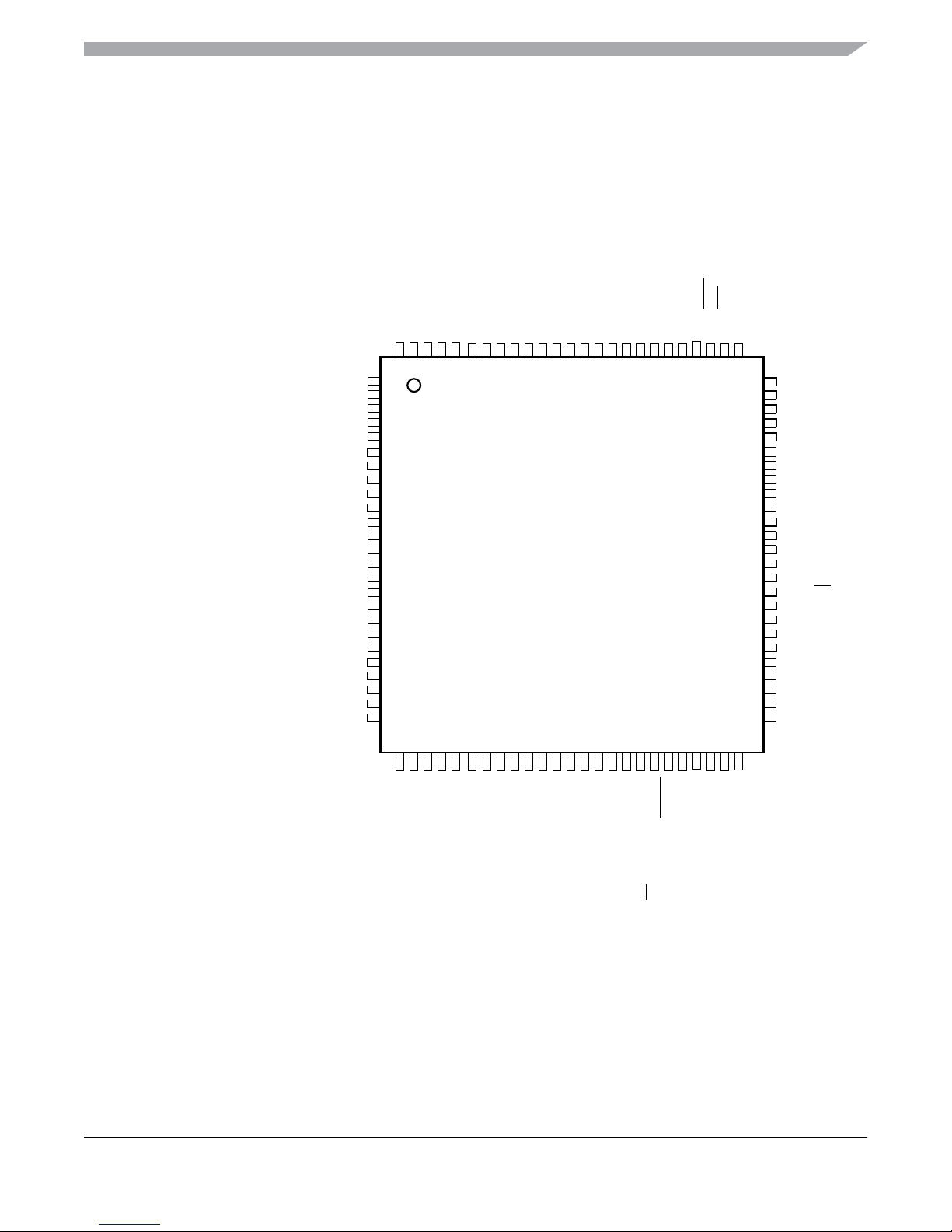
1.7.1 Device Pinout
MC9S12XHY-Family Reference Manual, Rev. 1.01
Freescale Semiconductor 27
Downloaded from Elcodis.com electronic components distributor
Page 28

Device Overview MC9S12XHY-Family
PAD04 /AN04 /KWAD4
PAD03 /AN03 /KWAD3
PAD02 /AN02 /KWAD2
PAD01 /AN01 /KWAD1
PAD00 /AN00 /KWAD0
VDDA /VRH
VSSA /VRL
BKGD /MODC
VLCD
PB7 /BP3
PB6 /BP2
PB5 /BP1
PB4 /BP0
VDD
VSS2
PB3 /FP39
PB2 /FP38
PB1 /FP37
PA7 /FP36
PA6 /FP35
PA5 /FP34
PA4 /FP33
PA3 /API_EXTCLK /XCLKS /FP32
PA2 /FP31
PA1 /XIRQ /FP30
PA0 /IRQ /FP29
PB0 /FP28
PR7 /FP27
KWAD5 /AN05 /PAD05
KWAD6 /AN06 /PAD06
KWAD7 /AN07 /PAD07
AN08 /PAD08
AN09 /PAD09
AN10 /PAD10
AN11 /PAD11
TEST
M0COSM /M0C0M /IOC0_0 /PU0
M0COSP /M0C0P /PU1
M0SINM /M0C1M /IOC0_1 /PU2
M0SINP /M0C1P /PU3
VDDM1
VSSM1
M1COSM /M1C0M /IOC0_2 /PU4
M1COSP /M1C0P /PU5
M1SINM /M1C1M /IOC0_3 /PU6
M1SINP /M1C1P /PU7
M2COSM /M2C0M /IOC0_4 /IOC1_0 /SCL /PWM4 /MISO /PV0
M2COSP /M2C0P /MOSI /PWM5 /PV1
M2SINM /M2C1M /IOC0_5 /IOC1_1 /SCK /PWM6 /PV2
M2SINP /M2C1P /SDA /PWM7 /SS /PV3
VDDM2
VSSM2
M3COSM /M3C0M /IOC0_6 /IOC1_2 /PV4
M3COSP /M3C0P /PV5
M3SINM /M3C1M /IOC0_7 /IOC1_3 /PV6
M3SINP /M3C1P /PV7
112
111
110
109
108
107
106
105
104
1
103
999897969594939291908988878685
102
101
100
2
3
4
5
6
7
8
9
10
11
MC9S12XHY-Family
112LQFP
12
13
14
15
16
17
18
19
Pins shown in BOLD are not
availableon the 100 LQFP package
20
21
22
23
24
25
26
27
28
293031323334353637383940414243444546474849505152535455
84
PH7 /FP26
83
PH6 /FP25
82
VDDPLL
81
XTAL
80
EXTAL
79
VSSPLL
78
VSS3
77
VDDR
76
PH5 /FP24
75
PH4 /FP23
74
VDDX1
73
VSSX1
72
PM3 /PWM7 /IOC1_3
71
PM2 /PWM6 /IOC1_2
70
PM1 /PWM5 /IOC0_3 /TXD1
69
PM0 /PWM4 /IOC0_2 /RXD1
68
VSS1
67
VDDF
66
PH3 /SS/ FP22
65
PH2 /ECLK /SCK /FP21
64
PH1 /MOSI /TXD1 /FP20
63
PH0 /MISO /RXD1 /FP19
62
PR6 /SCL /FP18
61
PR5 /SDA /FP17
60
PT7 /IOC0_7 /KWT7 /FP16
59
PT6 /IOC0_6 /KWT6 /FP15
58
PT5 /IOC0_5 /KWT5 /FP14
57
PT4 /IOC0_4 /KWT4 /FP13
56
Figure 1-3. MC9S12XHY-Family 112 LQFP pinout
MC9S12XHY-Family Reference Manual, Rev. 1.01
28 Freescale Semiconductor
Downloaded from Elcodis.com electronic components distributor
FP0 /PWM0 /PP0
FP1 /PWM1 /PP1
FP2 /PWM2 /PP2
FP3 /PWM3 /PP3
FP4 /PWM4 /PP4
FP5 /PWM5 /PP5
FP6 /PWM6 /PP6
FP7 /PWM7 /PP7
VSSX2
TXD0 /PWM7 /PS1
RXD0 /PWM6 /PS0
KWR2 /IOC1_6 /PR2
KWR3 /IOC1_7 /PR3
VDDX2
MISO /SCL /PWM0 /PS4
KWS3 /TXCAN0 /PWM5 /PS3
KWS2 /RXCAN0 /PWM4 /PS2
KWS5 /MOSI /PWM1 /PS5
KWR1 /TXCAN1 /IOC0_7 /PR1
KWR0 /RXCAN1 /IOC0_6 /PR0
RESET
SS /SDA /PWM3 /PS7
KWS6 /SCK /PWM2 /PS6
FP8 /KWT0 /IOC1_4 /PT0
FP9 /KWT1 /IOC1_5 /PT1
FP10 /KWT2 /IOC1_6 /PT2
FP12 /KWR4 /PR4
FP11 /KWT3 /IOC1_7 /PT3
Page 29
PAD04 /AN04 /KWAD4
PAD03 /AN03 /KWAD3
PAD02 /AN02 /KWAD2
PAD01 /AN01 /KWAD1
PAD00 /AN00 /KWAD0
VDDA /VRH
VSSA /VRL
BKGD /MODC
VLCD
PB7 /BP3
PB6 /BP2
PB5 /BP1
PB4 /BP0
VDD
VSS2
Device Overview MC9S12XHY-Family
PA0 /IRQ /FP29
PB1 /FP37
PA7 /FP36
PA6 /FP35
PA5 /FP34
PA4 /FP33
PA3 /API_EXTCLK /XCLKS /FP32
PA2 /FP31
PA1 /XIRQ /FP30
PB0 /FP28
KWAD5 /AN05 /PAD05
KWAD6 /AN06 /PAD06
KWAD7 /AN07 /PAD07
TEST
M0COSM /M0C0M /IOC0_0 /PU0
M0COSP /M0C0P /PU1
M0SINM /M0C1M /IOC0_1 /PU2
M0SINP /M0C1P /PU3
VDDM1
VSSM1
M1COSM /M1C0M /IOC0_2 /PU4
M1COSP /M1C0P /PU5
M1SINM /M1C1M /IOC0_3 /PU6
M1SINP /M1C1P /PU7
M2COSM/M2C0M/IOC0_4/IOC1_0/SCL/PWM4/MISO/PV0
M2COSP /M2C0P /MOSI /PWM5 /PV1
M2SINM /M2C1M /IOC0_5 /IOC1_1 /SCK /PWM6 /PV2
M2SINP /M2C1P /SDA /PWM7 /SS /PV3
VDDM2
VSSM2
M3COSM /M3C0M /IOC0_6 /IOC1_2 /PV4
M3COSP /M3C0P /PV5
M3SINM /M3C1M /IOC0_7 /IOC1_3 /PV6
M3SINP /M3C1P /PV7
FP0 /PWM0 /PP0
9998979695949392919089888786858483828180797877
100
1
2
3
4
5
6
7
8
9
10
11
12
13
14
15
16
17
18
19
20
21
22
23
24
25
26272829303132333435363738394041424344454647484950
MC9S12XHY-Family
100 LQFP
VSSX2
VDDX2
RESET
76
PR7 /FP27
75
PH7 /FP26
74
PH6 /FP25
73
VDDPLL
72
XTAL
71
EXTAL
70
VSSPLL
69
VSS3
68
VDDR
67
PH5 /FP24
66
PH4 /FP23
65
VDDX1
64
VSSX1
63
VSS1
62
VDDF
61
PH3 /SS/ FP22
60
PH2 /ECLK /SCK /FP21
59
PH1 /MOSI /TXD1 /FP20
58
PH0 /MISO /RXD1 /FP19
57
PR6 /SCL /FP18
56
PR5 /SDA /FP17
55
PT7 /IOC0_7 /KWT7 /FP16
54
PT6 /IOC0_6 /KWT6 /FP15
53
PT5 /IOC0_5 /KWT5 /FP14
52
PT4 /IOC0_4 /KWT4 /FP13
51
Figure 1-4. MC9S12XHY-Family 100LQFP pinout
MC9S12XHY-Family Reference Manual, Rev. 1.01
Freescale Semiconductor 29
Downloaded from Elcodis.com electronic components distributor
FP1 /PWM1 /PP1
FP2 /PWM2 /PP2
FP3 /PWM3 /PP3
FP4 /PWM4 /PP4
FP5 /PWM5 /PP5
FP6 /PWM6 /PP6
FP7 /PWM7 /PP7
TXD0 /PWM7 /PS1
RXD0 /PWM6 /PS0
KWS3 /TXCAN0 /PWM5 /PS3
KWS2 /RXCAN0 /PWM4 /PS2
KWR0 /RXCAN1 /IOC0_6 /PR0
SS /SDA /PWM3 /PS7
MISO /SCL /PWM0 /PS4
KWS6 /SCK /PWM2 /PS6
FP8 /KWT0 /IOC1_4 /PT0
KWS5 /MOSI /PWM1 /PS5
KWR1 /TXCAN1 /IOC0_7 /PR1
FP9 /KWT1 /IOC1_5 /PT1
FP12 /KWR4 /PR4
FP10 /KWT2 /IOC1_6 /PT2
FP11 /KWT3 /IOC1_7 /PT3
Page 30

Device Overview MC9S12XHY-Family
1.7.2 Pin Assignment Overview
Table 1-5 provides a summary of which Ports are available for each package option. Routing of pin
functions is summarized in Table 1-6.
Table 1-5. Port Availability by Package Option
Port 112 LQFP 100 LQFP
Port AD/ADC Channels 12/12 8/8
Port A 8 8
Port B 8 6
Port H 8 8
Port P 8 8
Port R 8 6
Port S 8 8
Port T 8 8
Port U 8 8
Port V 8 8
Port M 4 0
Sum of Ports 88 76
I/O Power Pairs VDDM/VSSM 2/2 2/2
I/O Power Pairs VDDX/VSSX 2/2 2/2
I/O Power Pairs VDDA/VSSA
VREG Power Pairs VDDR/VSS3 1/1 1/1
VDD/VSS2 1/1 1/1
VDDF/VSSF 1/1 1/1
I/O Power Pair VDDPLL/VSSPLL 1/1 1/1
VLCD power 1 1
Sum of power pins 19 19
OSC pairs XTAL/EXTAL 1/1 1/1
other pins RESET/TEST/BKGD 1/1/1 1/1/1
1. VRH/VRL are sharing with VDDA/VSSA pins
(1)
1/1 1/1
MC9S12XHY-Family Reference Manual, Rev. 1.01
30 Freescale Semiconductor
Downloaded from Elcodis.com electronic components distributor
Page 31

Device Overview MC9S12XHY-Family
Table 1-6. Peripheral - Port Routing Options
IIC
TIM0
[7:6]
PR[6:5] O
PV[3,0] O
PS[7,4] X
PT[7:6] X
2-23
2-16
PR[1:0] O
PV6,PV4 O
PT[5:4] X
PV2,PV0 O
PU6,PU4 X
PM[1:0] O
PT[3:2] X
PR[3:2] O
PV6,PV4 X
TIM0
[5:4]
2-16
TIM0
[3:2]
2-72
TIM1
[7:6]
2-16
TIM1
[3:2]
2-79
SPI
(1)
PWM
[7:4]
PWM
[3:0]
SCI1
PM[3:2] O
PS[7:4] X
2-23
PV[3:0] O
PH[3:0] O
PP[7:4] X
2-36
PS[1:0,3:2] O
PV[3:0] O
PM[3:0] O
PP[3:0] X
2-37
PS[7:4] O
PH[1:0] X
2-45
PM[1:0] O
1. “O” denotes a possible rerouting under software control, “X” denotes as default routing option
Table 1-7 provides a pin out summary listing the availability and functionality of individual pins for each
package option.
MC9S12XHY-Family Reference Manual, Rev. 1.01
Freescale Semiconductor 31
Downloaded from Elcodis.com electronic components distributor
Page 32

Device Overview MC9S12XHY-Family
MC9S12XHY-Family Reference Manual, Rev. 1.01
Freescale Semiconductor 32
Table 1-7. Pin-Out Summary
(1)
Package
Pin
Function
Power
Supply
Internal Pull
Resistor
Description
LQ
FP
100
LQ
FP64Pin
2nd
Func.
3rd
Func
.
4th
Func
.
5th
Func
.
6th
Func
.
7th
Func
.
8th
Func
.
CTRL
Reset
State
1 1 PAD05 AN05
KWA
D5
VDDA PERAD
Dis-
abled
Port AD I/O, analog input of
ATD, key wakeup
2 2 PAD06 AN06
KWA
D6
VDDA PERAD
Disabled
Port AD I/O, analog input of
ATD, key wakeup
3 3 PAD07 AN07
KWA
D7
VDDA PERAD
Disabled
Port AD I/O, analog input of
ATD, key wakeup
4 - PAD08 AN08 VDDA PERAD
Disabled
Port AD I/O, analog input of
ATD
5 - PAD09 AN09 VDDA PERAD
Disabled
Port AD I/O, analog input of
ATD
6 - PAD10 AN10 VDDA PERAD
Disabled
Port AD I/O, analog input of
ATD
7 - PAD11 AN11 VDDA PERAD
Disabled
Port AD I/O, analog input of
ATD
8 4 TEST VDDA
RESET
pin
DOW
N
Test input
9 5 PU0
IOC0
_0
M0C0MM0C
OSM
VDDM
PERU/P
PSU
Disabled
Port U I/O, Motor0 coil
nodes of MC,TIM0 channel
10 6 PU1
M0C0PM0C
OSP
VDDM
PERU/P
PSU
Disabled
Port U I/O, Motor0 coil
nodes of MC
11 7 PU2
IOC0
_1
M0C1MM0SI
NM
VDDM
PERU/P
PSU
Disabled
Port U I/O, Motor0 coil
nodes of MC,TIM0 channel
12 8 PU3
M0C1PM0SI
NP
VDDM
PERU/P
PSU
Disabled
Port U I/O, Motor0 coil
nodes of MC
Downloaded from Elcodis.com electronic components distributor
Page 33

Device Overview MC9S12XHY-Family
MC9S12XHY-Family Reference Manual, Rev. 1.01
Freescale Semiconductor 33
13 9 VDDM1
14 10 VSSM1
15 11 PU4
IOC0
_2
M1C0MM1C
OSM
VDDM
PERU/P
PSU
Disabled
Port U I/O, Motor1 coil
nodes of MC,TIM0 channel
16 12 PU5
M1C0PM1C
OSP
VDDM
PERU/P
PSU
Disabled
Port U I/O, Motor1 coil
nodes of MC
17 13 PU6
IOC0
_3
M1C1MM1SI
NM
VDDM
PERU/P
PSU
Disabled
Port U I/O, Motor1 coil
nodes of MC,TIM0 channel
18 14 PU7
M1C1PM1SI
NP
VDDM
PERU/P
PSU
Disabled
Port U I/O, Motor1 coil
nodes of MC
19 15 PV0 MISO
PW
M4
SCL
IOC1_0IOC0_4M2C0MM2C
OSM
VDDM
PERV/P
PSV
Disabled
Port V I/O, Motor2 coil
nodes of MC, MISO of SPI,
SCL of IIC, PWM channel
4,TIM0/1 channel
20 16 PV1 PWM5
MOS
I
M2C0PM2C
OSP
VDDM
PERV/P
PSV
Disabled
Port V I/O, Motor2 coil
nodes of MC, MOSI of SPI,
PWM channel 5
21 17 PV2 PWM6 SCK
IOC1_1IOC0_5M2C1MM2SI
NM
VDDM
PERV/P
PSV
Disabled
Port V I/O, Motor2 coil
nodes of MC, SCK of SPI,
PWM channel 6,TIM0/1
channel
22 18 PV3 SS
PW
M7
SDA
M2C1PM2SI
NP
VDDM
PERV/P
PSV
Disabled
Port V I/O, Motor2 coil
nodes of MC, SS of SPI
SDA of IIC, PWM channel 7
23 19 VDDM2
24 20 VSSM2
Table 1-7. Pin-Out Summary
(1)
Package
Pin
Function
Power
Supply
Internal Pull
Resistor
Description
LQ
FP
100
LQ
FP64Pin
2nd
Func.
3rd
Func
.
4th
Func
.
5th
Func
.
6th
Func
.
7th
Func
.
8th
Func
.
CTRL
Reset
State
Downloaded from Elcodis.com electronic components distributor
Page 34

Device Overview MC9S12XHY-Family
MC9S12XHY-Family Reference Manual, Rev. 1.01
Freescale Semiconductor 34
25 21 PV4
IOC1_2IOC0_6M3C0MM3C
OSM
VDDM
PERV/P
PSV
Disabled
Port V I/O, Motor3 coil
nodes of MC,TIM0/1 chan-
nel
26 22 PV5
M3C0PM3C
OSP
VDDM
PERV/P
PSV
Disabled
Port V I/O, Motor3 coil
nodes of MC
27 23 PV6
IOC1_3IOC0_7M3C1MM3SI
NM
VDDM
PERV/P
PSV
Disabled
Port V I/O, Motor3 coil
nodes of MC,TIM0/1 chan-
nel
28 24 PV7
M3C1PM3SI
NP
VDDM
PERV/P
PSV
Disabled
Port V I/O, Motor3 coil
nodes of MC
29 25 PP0 PWM0 FP0 VDDX
PERP/P
PSP
Down
Port R I/O, timer1 Channel,
Key wakeup
30 26 PP1 PWM1 FP1 VDDX
PERP/P
PSP
Down
Port R I/O, timer1 Channel,
Key wakeup
31 27 PP2 PWM2 FP2 VDDX
PERP/P
PSP
Down
Port P I/O, LCD Frontplane
driver, PWM channel
32 28 PP3 PWM3 FP3 VDDX
PERP/P
PSP
Down
Port P I/O, LCD Frontplane
driver, PWM channel
33 29 PP4 PWM4 FP4 VDDX
PERP/P
PSP
Down
Port P I/O, LCD Frontplane
driver, PWM channel
34 30 PP5 PWM5 FP5 VDDX
PERP/P
PSP
Down
Port P I/O, LCD Frontplane
driver, PWM channel
35 31 PP6 PWM6 FP6 VDDX
PERP/P
PSP
Down
Port P I/O, LCD Frontplane
driver, PWM channel
36 32 PP7 PWM7 FP7 VDDX
PERP/P
PSP
Down
Port P I/O, LCD Frontplane
driver, PWM channel
Table 1-7. Pin-Out Summary
(1)
Package
Pin
Function
Power
Supply
Internal Pull
Resistor
Description
LQ
FP
100
LQ
FP64Pin
2nd
Func.
3rd
Func
.
4th
Func
.
5th
Func
.
6th
Func
.
7th
Func
.
8th
Func
.
CTRL
Reset
State
Downloaded from Elcodis.com electronic components distributor
Page 35

Device Overview MC9S12XHY-Family
MC9S12XHY-Family Reference Manual, Rev. 1.01
Freescale Semiconductor 35
37 - PR2
IOC1_6KWR
2
VDDX
PERR/P
PSR
Down
Port R I/O, timer1 Channel,
Key wakeup
38 - PR3
IOC1_7KWR
3
VDDX
PERR/P
PSR
Down
Port R I/O, timer1 Channel,
Key wakeup
39 33 PS0 PWM6
RXD
0
VDDX
PERS/P
PSS
Up
Port S I/O, RXD of SCI0,
PWM channel6
40 34 PS1 PWM7
TXD
0
VDDX
PERS/P
PSS
Up
Port S I/O, TXD of SCI0,
PWM channel 7
41 35 VSSX2
42 36 VDDX2
43 37 PS2 PWM4
RXC
AN0
KWS
2
VDDX
PERS/P
PSS
Up
Port S I/O, PWM channel
4,RX of CAN0 , Key wakeup
44 38 PS3 PWM5
TXC
AN0
KWS
3
VDDX
PERS/P
PSS
Up
Port S I/O,PWM channel 5,
TX of CAN0 , Key wakeup
45 39 PR0
IOC0_6RXC
AN1
KWR
0
VDDX
PERR/P
PSR
Down
Port R I/O, timer0 Chan-
nel,RX of CAN1,Key
wakeup
46 40 PR1
IOC0_7TXC
AN1
KWR
1
VDDX
PERR/P
PSR
Down
Port R I/O, timer0 Chan-
nel,TX of CAN1 ,Key
wakeup
47 41 PS4 PWM0 SCL
MIS
O
VDDX
PERS/P
PSS
Up
Port S I/O, MISO of SPI,
SCL of IIC, PWM channel 0
48 42 PS5 PWM1
MOS
I
KWS
5
VDDX
PERS/P
PSS
Up
Port S I/O, MOSI of SPI,
PWM channel 1, key
wakeup
Table 1-7. Pin-Out Summary
(1)
Package
Pin
Function
Power
Supply
Internal Pull
Resistor
Description
LQ
FP
100
LQ
FP64Pin
2nd
Func.
3rd
Func
.
4th
Func
.
5th
Func
.
6th
Func
.
7th
Func
.
8th
Func
.
CTRL
Reset
State
Downloaded from Elcodis.com electronic components distributor
Page 36

Device Overview MC9S12XHY-Family
MC9S12XHY-Family Reference Manual, Rev. 1.01
Freescale Semiconductor 36
49 43 PS6 PWM2 SCK
KWS
6
VDDX
PERS/P
PSS
Up
Port S I/O, SCK of SPI,
PWM channel2 , key
wakeup
50 44 PS7 PWM3 SDA SS VDDX
PERS/P
PSS
Up
Port S I/O, SS of SPI, SDA
of IIC, PWM channel 3
51 45 RESET VDDX PULLUP External reset
52 46 PT0
IOC1_4KWT
0
FP8 VDDX
PERT/P
PST
Down
Port T I/O, LCD Frontplane
driver, timer1 channel, key
wakeup
53 47 PT1
IOC1_5KWT
1
FP9 VDDX
PERT/P
PST
Down
Port T I/O, LCD Frontplane
driver, timer1 channel, key
wakeup
54 48 PT2
IOC1_6KWT
2
FP10 VDDX
PERT/P
PST
Down
Port T I/O, LCD Frontplane
driver, timer1 channel, key
wakeup
55 49 PT3
IOC1_7KWT
3
FP11 VDDX
PERT/P
PST
Down
Port T I/O, LCD Frontplane
driver, timer1 channel, key
wakeup
56 50 PR4 KWR4 FP12 VDDX
PERR/P
PSR
Down
Port R I/O, LCD Frontplane
driver , Key wakeup
57 51 PT4
IOC0_4KWT
4
FP13 VDDX
PERT/P
PST
Down
Port T I/O, LCD Frontplane
driver, timer0 channel, key
wakeup
58 52 PT5
IOC0_5KWT
5
FP14 VDDX
PERT/P
PST
Down
Port T I/O, LCD Frontplane
driver, timer0 channel, key
wakeup
Table 1-7. Pin-Out Summary
(1)
Package
Pin
Function
Power
Supply
Internal Pull
Resistor
Description
LQ
FP
100
LQ
FP64Pin
2nd
Func.
3rd
Func
.
4th
Func
.
5th
Func
.
6th
Func
.
7th
Func
.
8th
Func
.
CTRL
Reset
State
Downloaded from Elcodis.com electronic components distributor
Page 37

Device Overview MC9S12XHY-Family
MC9S12XHY-Family Reference Manual, Rev. 1.01
Freescale Semiconductor 37
59 53 PT6
IOC0_6KWT
6
FP15 VDDX
PERT/P
PST
Down
Port T I/O, LCD Frontplane
driver, timer0 channel,key
wakeup
60 54 PT7
IOC0_7KWT
7
FP16 VDDX
PERT/P
PST
Down
Port T I/O, LCD Frontplane
driver, timer0 channel, key
wakeup
61 55 PR5 SDA FP17 VDDX
PERR/P
PSR
Down
Port R I/O, LCD Frontplane
driver, SDA of IIC
62 56 PR6 SCL FP18 VDDX
PERR/P
PSR
Down
Port R I/O, LCD Frontplane
driver, SCL of IIC
63 57 PH0 MISO
RXD
1
FP19 VDDX
PERH/P
PSH
Down
Port H I/O, LCD Frontplane
driver, MISO of SPI, RXD of
SCI1
64 58 PH1 MOSI
TXD
1
FP20 VDDX
PERH/P
PSH
Down
Port HI/O, LCD Frontplane
driver, MOSI of SPI ,TXD of
SCI1
65 59 PH2 ECLK SCK FP21 VDDX
PERH/P
PSH
Down
Port HI/O, LCD Frontplane
driver, SCK of SPI, Bus
clock output
66 60 PH3 SS FP22 VDDX
PERH/P
PSH
Down
Port H I/O, LCD Frontplane
driver, SS of SPI
67 61 VDDF 0
68 62 VSS1 0
69 - PM0 PWM4
IOC0_2RXD
1
VDDX
PERM/P
PSM
Up
Port M I/O, PWM channel4 ,
timer0 Channe 2, RXD of
SCI1
Table 1-7. Pin-Out Summary
(1)
Package
Pin
Function
Power
Supply
Internal Pull
Resistor
Description
LQ
FP
100
LQ
FP64Pin
2nd
Func.
3rd
Func
.
4th
Func
.
5th
Func
.
6th
Func
.
7th
Func
.
8th
Func
.
CTRL
Reset
State
Downloaded from Elcodis.com electronic components distributor
Page 38

Device Overview MC9S12XHY-Family
MC9S12XHY-Family Reference Manual, Rev. 1.01
Freescale Semiconductor 38
70 - PM1 PWM5
IOC0_3TXD
1
VDDX
PERM/P
PSM
Up
Port M I/O, PWM channel5 ,
timer0 Channe 3, TXD of
SCI1
71 - PM2 PWM6
IOC1
_2
VDDX
PERM/P
PSM
Up
Port M I/O, PWM channel6 ,
timer1 Channe 2
72 - PM3 PWM7
IOC1
_3
VDDX
PERM/P
PSM
Up
Port M I/O, PWM channel7 ,
timer1 Channe 3
73 63 VSSX1
74 64 VDDX1
75 65 PH4 FP23 VDDX
PERH/P
PSH
Down
Port HI/O, LCD Frontplane
driver
76 66 PH5 FP24 VDDX
PERH/P
PSH
Down
Port H I/O, LCD Frontplane
driver
77 67 VDDR
78 68 VSS3
79 69
VSSPLL
80 70 EXTAL
VDDP
LL
OSCI0llator pin
81 71 XTAL
VDDP
LL
OSCI0llator pin
82 72
VDDPL
L
Table 1-7. Pin-Out Summary
(1)
Package
Pin
Function
Power
Supply
Internal Pull
Resistor
Description
LQ
FP
100
LQ
FP64Pin
2nd
Func.
3rd
Func
.
4th
Func
.
5th
Func
.
6th
Func
.
7th
Func
.
8th
Func
.
CTRL
Reset
State
Downloaded from Elcodis.com electronic components distributor
Page 39

Device Overview MC9S12XHY-Family
MC9S12XHY-Family Reference Manual, Rev. 1.01
Freescale Semiconductor 39
83 73 PH6 FP25 VDDX
PERH/P
PSH
Down
Port H I/O, LCD Frontplane
driver
84 74 PH7 FP26 VDDX
PERH/P
PSH
Down
Port H I/O, LCD Frontplane
driver
85 75 PR7 FP27 VDDX
PERR/P
PSR
Down
Port R I/O, LCD Frontplane
driver
86 76 PB0 FP28 VDDX PUCR Down
Port B I/O, LCD Frontplane
driver
87 77 PA0 IRQ FP29 VDDX PUCR Down
Port A I/O, LCD Frontplane
driver, API output
88 78 PA1 XIRQ FP30 VDDX PUCR Down
Port A I/O, LCD Frontplane
driver
89 79 PA2 FP31 VDDX PUCR Down
Port A I/O, LCD Frontplane
driver
90 80 PA3
API_E
XTCL
K
XCL
KS
FP32 VDDX PUCR Down
Port A I/O, LCD Frontplane
driver
91 81 PA4 FP33 VDDX PUCR Down
Port A I/O, LCD Frontplane
driver
92 82 PA5 FP34 VDDX PUCR Down
Port A I/O, LCD Frontplane
driver
93 83 PA6 FP35 VDDX PUCR Down
Port A I/O, LCD Frontplane
driver
94 84 PA7 FP36 VDDX PUCR Down
Port A I/O, LCD Frontplane
driver
Table 1-7. Pin-Out Summary
(1)
Package
Pin
Function
Power
Supply
Internal Pull
Resistor
Description
LQ
FP
100
LQ
FP64Pin
2nd
Func.
3rd
Func
.
4th
Func
.
5th
Func
.
6th
Func
.
7th
Func
.
8th
Func
.
CTRL
Reset
State
Downloaded from Elcodis.com electronic components distributor
Page 40

Device Overview MC9S12XHY-Family
MC9S12XHY-Family Reference Manual, Rev. 1.01
Freescale Semiconductor 40
95 85 PB1 FP37 VDDX PUCR Down
Port BI/O, LCD Frontplane
driver
96 - PB2 FP38 VDDX PUCR Down
Port B I/O, LCD Frontplane
driver
97 - PB3 FP39 VDDX PUCR Down
Port B I/O, LCD Frontplane
driver
98 86 VSS2
99 87 VDD
100 88 PB4 BP0 VDDX PUCR Down
Port B I/O, LCD Backplane
driver
101 89 PB5 BP1 VDDX PUCR Down
Port B I/O, LCD Backplane
driver
102 90 PB6 BP2 VDDX PUCR Down
Port B I/O, LCD Backplane
driver
103 91 PB7 BP3 VDDX PUCR Down
Port B I/O, LCD Backplane
driver
104 92 VLCD VDDX
Voltagereference pin for the
LCD driver.
105 93 BKGD MODC VDDX
Always
on
Up
Background debug, Mode
selection pin
106 94 VSSA VRL
107 95 VDDA VRH
108 96 PAD00 AN00
KWA
D0
VDDA PERAD
Disabled
Port AD I/O, analog input of
ATD, key wakeup
Table 1-7. Pin-Out Summary
(1)
Package
Pin
Function
Power
Supply
Internal Pull
Resistor
Description
LQ
FP
100
LQ
FP64Pin
2nd
Func.
3rd
Func
.
4th
Func
.
5th
Func
.
6th
Func
.
7th
Func
.
8th
Func
.
CTRL
Reset
State
Downloaded from Elcodis.com electronic components distributor
Page 41

Device Overview MC9S12XHY-Family
MC9S12XHY-Family Reference Manual, Rev. 1.01
Freescale Semiconductor 41
NOTE
For devices assembled in 100-pin package all non-bonded out pins should be configured as outputs after
reset in order to avoid current drawn from floating inputs. Refer to Table 1-7 for affected pins.
109 97 PAD01 AN01
KWA
D1
VDDA PERAD
Disabled
Port AD I/O, analog input of
ATD, key wakeup
110 98 PAD02 AN02
KWA
D2
VDDA PERAD
Disabled
Port AD I/O, analog input of
ATD, key wakeup
111 99 PAD03 AN03
KWA
D3
VDDA PERAD
Disabled
Port AD I/O, analog input of
ATD, key wakeup
112
10
0
PAD04 AN04
KWA
D4
VDDA PERAD
Disabled
Port AD I/O, analog input of
ATD, key wakeup
1. Table shows a superset of pin functions. Not all functions are available on all derivatives
2. When Routing the IIC to PR/PH port, in order to overwrite the internal pull-down during reset, the external IIC pull-up resistor should be < =4.7K
3. When
IRQ/XIRQ is enabled, the internal pulldown function will be disabled, the external pullup resistor is required
Table 1-7. Pin-Out Summary
(1)
Package
Pin
Function
Power
Supply
Internal Pull
Resistor
Description
LQ
FP
100
LQ
FP64Pin
2nd
Func.
3rd
Func
.
4th
Func
.
5th
Func
.
6th
Func
.
7th
Func
.
8th
Func
.
CTRL
Reset
State
Downloaded from Elcodis.com electronic components distributor
Page 42

Device Overview MC9S12XHY-Family
1.7.3 Detailed Signal Descriptions
1.7.3.1 EXTAL, XTAL — Oscillator Pins
EXTAL and XTAL are the crystal driver and external clock pins. On reset all the device clocks are derived
from the internal reference clock. XTAL is the oscillator output.
1.7.3.2 RESET — External Reset Pin
The RESET pin is an active low bidirectional control signal. It acts as an input to initialize the MCU to a
known start-up state, and an output when an internal MCU function causes a reset. The
internal pull-up device.
1.7.3.3 TEST — Test Pin
This input only pin is reserved for factory test. This pin has an internal pull-down device.
NOTE
The TEST pin must be tied to V
in all applications.
SSA
RESET pin has an
1.7.3.4 BKGD / MODC — Background Debug and Mode Pin
The BKGD/MODC pin is used as a pseudo-open-drain pin for the background debug communication. It
is used as a MCU operating mode select pin during reset. The state of this pin is latched to the MODC bit
at the rising edge of
RESET. The BKGD pin has an internal pull-up device.
1.7.3.5 PAD[7:0] / AN[7:0] / KWAD[7:0]— Port AD Input Pins of ATD [7:0]
PAD[7:0] are a general-purpose input or output pins and analog inputs AN[7:0] of the analog-to-digital
converter ATD. They can be configured as keypad wakeup inputs.
1.7.3.6 PA[7:4] / FP[36:33]— Port A I/O Pins [7:4]
PA[7:4] are a general-purpose input or output pins. They can be configured as frontplane segment driver
outputs FP[36:33].
1.7.3.7 PA[3:2] / API_EXTCLK / XCLKS / FP[32:31]— Port A I/O Pins [3:2]
PA[3:2] are a general-purpose input or output pins. They can be configured as frontplane segment driver
outputs FP[32:31]. PA3 can also be configure as API_EXTCLK.The XCLKS is an input signal which
controls whether a crystal in combination with the internal loop controlled Pierce oscillator is used or
whether full swing Pierce oscillator/external clock circuitry is used (refer to Section 1.16, “Oscillator
Configuration ). An internal pull-down is enabled during reset.
MC9S12XHY-Family Reference Manual, Rev. 1.01
42 Freescale Semiconductor
Downloaded from Elcodis.com electronic components distributor
Page 43

Device Overview MC9S12XHY-Family
1.7.3.8 PA1 / XIRQ / FP[30]— Port A I/O Pin 1
PA1 is a general-purpose input or output pin. It can be configured as frontplane segment driver outputs
FP[30]. It also provide the non-maskable interrupt request input that provides a means of applying
asynchronous interrupt requests. This will wake up the MCU from stop or wait mode. The XIRQ interrupt
is level sensitive and active low. As XIRQ is level sensitive, while this pin is low the MCU will not enter
STOP mode. After Reset, the XIRQ default is not enabled.
1.7.3.9 PA0 / IRQ / FP[29]— Port A I/O Pin 0
PA0 is a general-purpose input or output pin. It can be configured as frontplane segment driver outputs
FP[29].Tthe maskable interrupt request input that provides a means of applying asynchronous interrupt
requests.
1.7.3.10 PB[7:4] / BP[3:0] — Port B I/O Pins [7:4]
PB[7:4] are a general-purpose input or output pins. They can be configured as backplane segment driver
output BP[3:0].
1.7.3.11 PB[3:0] / FP[39:37,28] — Port B I/O Pins [3:0]
PB[3:0] are a general-purpose input or output pins. They can be configured as frontplane segment driver
output FP[
39:37,28].
1.7.3.12 PS7 / PWM3 / SDA / SS — Port S I/O Pin 7
PS7 is a general-purpose input or output pin. It can be configured as the slave selection pin SS for the serial
peripheral interface (SPI). It can be configured as the serial data pin SDA as IIC module. It can be
configured as PWM channel 3.
1.7.3.13 PS6 / PWM2 / SCK / KWS6 — Port S I/O Pin 6
PS6 is a general-purpose input or output pin. It can be configured as the serial clock SCK of the serial
peripheral interface (SPI). It can be configured as PWM channel 2. It can be configured as keypad wakeup
input.
1.7.3.14 PS5 / PWM1 / MOSI / KWS5 — Port S I/O Pin 5
PS5 is a general-purpose input or output pin. It can be configured as the master output (during master
mode) or slave input pin (during slave mode) MOSI of the serial peripheral interface (SPI). It can be
configured as PWM channel1. It can configured as keypad wakeup input.
1.7.3.15 PS4 / PWM0 / SCL / MISO — Port S I/O Pin 4
PS4 is a general-purpose input or output pin. It can be configured as the master input (during master mode)
or slave output pin (during slave mode) MISO for the serial peripheral interface (SPI).It can be configured
as the serial clock pin SCL as IIC module.It can be configured as PWM channel0
MC9S12XHY-Family Reference Manual, Rev. 1.01
Freescale Semiconductor 43
Downloaded from Elcodis.com electronic components distributor
Page 44

Device Overview MC9S12XHY-Family
1.7.3.16 PS3 / PWM5 / TXCAN / KWS3 — Port S I/O Pin 3
PS3 is a general-purpose input or output pin. It can be configured as the transmit pin TXCAN of the
scalable controller area network controller (CAN). It can be configured as PWM channel5. It can
configured as keypad wakeup input.
1.7.3.17 PS2 / PWM4 / RXCAN / KWS2 — Port S I/O Pin 2
PS3 is a general-purpose input or output pin. It can be configured as the receive pin RXCAN of the scalable
controller area network controller (CAN). It can be configured as PWM channel4. It can configured as
keypad wakeup input.
1.7.3.18 PS1 / PWM7 / TXD — Port S I/O Pin 1
PS1 is a general-purpose input or output pin. It can be configured as the transmit pin TXD of serial
communication interface(SCI). It can be configured as PWM channel 7.
1.7.3.19 PS0 / PWM6 / RXD — Port S I/O Pin 0
PS0 is a general-purpose input or output pin. It can be configured as the receive pin RXD of serial
communication interface(SCI). It can be configured as PWM channel 6.
1.7.3.20 PR7 / FP[27] — Port R I/O Pin 7
PR7 is a general-purpose input or output pin. It can be configured as frontplane segment driver output
FP[27].
1.7.3.21 PR6 / SCL / FP[18]— Port R I/O Pin 6
PR6 is a general-purpose input or output pin. It can be configured as frontplane segment driver output
FP[18]. It can be configured as the serial clock pin SCL of IIC.
1.7.3.22 PR5 / SDA / FP[17]— Port R I/O Pin 5
PR5 is a general-purpose input or output pin. It can be configured as frontplane segment driver output
FP[17]. It can be configured as the serial data pin SDA of IIC.
1.7.3.23 PR4 / KWR4 / FP[12] — Port R I/O Pin 4
PR4 is a general-purpose input or output pin. It can be configured as frontplane segment driver output
FP[12].They can be configured as keypad wakeup inputs.
1.7.3.24 PR[3:2] / IOC1[7:6] / KWR[3:2] — Port R I/O Pins [3:2]
PR[3:2] are a general-purpose input or output pins. They can be configured as timer (TIM1) channel 7-6.
They can be configured as keypad wakeup inputs.
MC9S12XHY-Family Reference Manual, Rev. 1.01
44 Freescale Semiconductor
Downloaded from Elcodis.com electronic components distributor
Page 45

Device Overview MC9S12XHY-Family
1.7.3.25 PR1 / IOC0_7 / TXCAN1 / KWR1 — Port R I/O Pins 1
PR[1:0] are a general-purpose input or output pins. They can be configured as timer (TIM0) channel 7-6.
It can be configured as the transmit pin TXCAN of the scalable controller area network controller
(CAN1).They can be configured as keypad wakeup inputs.
1.7.3.26 PR0 / IOC0_6 / RXCAN1 / KWR0 — Port R I/O Pins 0
PR[1:0] are a general-purpose input or output pins. They can be configured as timer (TIM0) channel 7-6.
It can be configured as the receive pin RXCAN of the scalable controller area network controller
(CAN1).They can be configured as keypad wakeup inputs.
1.7.3.27 PP[7:0] / PWM[7:0] / FP[7:0] — Port P I/O Pins [7:0]
PP[7:0] are a general-purpose input or output pins. They can be configured as frontplane segment driver
output FP[7:0]. They can be configured as pulse width modulator (PWM) channel 7-0 output.
1.7.3.28 PH[7:4] / FP[26:23] — Port H I/O Pins [7:4]
PH[7:4] are a general-purpose input or output pins. They can be configured as frontplane segment driver
output FP[26:23].
1.7.3.29 PH3 / SS / FP[22]— Port H I/O Pin 3
PH3 is a general-purpose input or output pin. It can be configured as frontplane segment driver output
FP[22]. It can be configured as the slave selection pin
SS for the serial peripheral interface (SPI).
1.7.3.30 PH2 / ECLK / SCK / FP[21] — Port H I/O Pin 2
PH2 is a general-purpose input or output pin. It can be configured as frontplane segment driver output
FP[21]. It can be configured as the serial clock SCK of the serial peripheral interface (SPI). It can be
configured to drive the internal bus clock ECLK. ECLK can be used as a timing reference. The ECLK
output has a programmable prescaler.
1.7.3.31 PH1 / MOSI / TXD1 / FP[20] — Port H I/O Pin 1
PH1 is a general-purpose input or output pin. It can be configured as frontplane segment driver output
FP[20]. It can be configured as the master output (during master mode) or slave input pin (during slave
mode) MOSI of the serial peripheral interface (SPI).It can be configured as the transmitpin TXD of serial
communication interface(SCI1).
1.7.3.32 PH0 / MISO / RXD1 / FP[19] — Port H I/O Pin 0
PH0 is a general-purpose input or output pin. It can be configured as frontplane segment driver output
FP[19]. It can be configured as the master input (during master mode) or slave output pin (during slave
mode) MISO for the serial peripheral interface (SPI).It can be configured as the receive pin RXD of serial
communication interface(SCI1).
MC9S12XHY-Family Reference Manual, Rev. 1.01
Freescale Semiconductor 45
Downloaded from Elcodis.com electronic components distributor
Page 46

Device Overview MC9S12XHY-Family
1.7.3.33 PT[7:4] / IOC0[7:4] / KWT[7:4] / FP[16:13] — Port T I/O Pins [7:4]
PT[7:4] are a general-purpose input or output pins. They can be configured as frontplane segment driver
output FP[16:13]. They can be configured as timer (TIM0) channel 7-4. They can be configured as key
wakeup inputs.
1.7.3.34 PM3 / PMW7 / IOC1_3 — Port M I/O Pins [3]
PM3 is a general-purpose input or output pin. . It can be configured as timer (TIM1) channels 3.It can be
configured as PWM channel7.
1.7.3.35 PM2 / PMW6 / IOC1_2 — Port M I/O Pins [2]
PM2 is a general-purpose input or output pin. .It can be configured as timer (TIM1) channels 2. It can be
configured as PWM channel6.
1.7.3.36 PM1 / PMW5 / IOC0_3 / TXD1— Port M I/O Pins [1]
PM1 is a general-purpose input or output pin. It can be configured as the transmitpin TXD of serial
communication interface(SCI). It can be configured as timer (TIM0) channels 3.It can be configured as
PWM channel5.
1.7.3.37 PM0 / PMW4 / IOC0_2 / RXD1— Port M I/O Pins [0]
PM0 is a general-purpose input or output pin. It can be configured as the receive pin RXD of serial
communication interface(SCI).It can be configured as timer (TIM0) channels 2. It can be configured as
PWM channel4.
1.7.3.38 PT[3:0] / IOC1[7:4] /KWT [3:0] / FP[11:8] — Port T I/O Pin [3:0]
PT[3:0] are a general-purpose input or output pins. They can be configured as frontplane segment driver
output FP[11:8]. They can be configured as timer (TIM1) channels 7-4. They can be configured as key
wakeup inputs.
1.7.3.39 PU[7] / M1C1P / M1SINP — Port U I/O Pin [7]
PU[7] is a general-purpose input or output pin. It can be configured as high current PWM output pin which
can be used for motor drive or to measure the back EMF to calibrate the pointer reset position. The pin
interfaces to the coils of motor 1.
1.7.3.40 PU[6] / IOC0_3 / M1C1M / M1SINM — Port U I/O Pin [6]
PU[6] is a general-purpose input or output pin. It can be configured as high current PWM output pin which
can be used for motor drive or to measure the back EMF to calibrate the pointer reset position. The pin
interfaces to the coils of motor 1. It can aslo be configured as timer (TIM0) channel 3
MC9S12XHY-Family Reference Manual, Rev. 1.01
46 Freescale Semiconductor
Downloaded from Elcodis.com electronic components distributor
Page 47

Device Overview MC9S12XHY-Family
1.7.3.41 PU[5] / M1C0P / M1COSP— Port U I/O Pin [5]
PU[5] is a general-purpose input or output pin. It can be configured as high current PWM output pin which
can be used for motor drive or to measure the back EMF to calibrate the pointer reset position. The pin
interfaces to the coils of motor 1.
1.7.3.42 PU[4] / IOC0_2 / M1C0M / M1SINP— Port U I/O Pin [4]
PU[4] is a general-purpose input or output pin. It can be configured as high current PWM output pin which
can be used for motor drive or to measure the back EMF to calibrate the pointer reset position. The pin
interfaces to the coils of motor 1. It can aslo be configured as timer (TIM0) channel 2
1.7.3.43 PU[3] / M0C1P / M0SINP— Port U I/O Pin [3]
PU[3] is a general-purpose input or output pin. It can be configured as high current PWM output pin which
can be used for motor drive or to measure the back EMF to calibrate the pointer reset position. The pin
interfaces to the coils of motor 0.
1.7.3.44 PU[2] / IOC0_1 / M0C1M / M0SINM — Port U I/O Pin [2]
PU[2] is a general-purpose input or output pin. It can be configured as high current PWM output pin which
can be used for motor drive or to measure the back EMF to calibrate the pointer reset position. The pin
interfaces to the coils of motor 0. It can aslo be configured as timer(TIM0) channel 1
1.7.3.45 PU[1] / M0C0P / M0COSP— Port U I/O Pin [1]
PU[1] is a general-purpose input or output pin. It can be configured as high current PWM output pin which
can be used for motor drive or to measure the back EMF to calibrate the pointer reset position. The pin
interfaces to the coils of motor 0.
1.7.3.46 PU[0] / IOC0_0 / M0C0M / M0COSM— Port U I/O Pin [0]
PU[0] is a general-purpose input or output pin. It can be configured as high current PWM output pin which
can be used for motor drive or to measure the back EMF to calibrate the pointer reset position. The pin
interfaces to the coils of motor 0. It can aslo be configured as timer(TIM0) channel 0
1.7.3.47 PV[7] / M3C1P / M3SINP— Port V I/O Pin [7]
PV[7] is a general-purpose input or output pin. It can be configured as high current PWM output pin which
can be used for motor drive or to measure the back EMF to calibrate the pointer reset position. The pin
interfaces to the coils of motor 3.
1.7.3.48 PV[6] / IOC1_3 / IOC0_7 / M3C1M / M3SINM — Port V I/O Pin [6]
PV[6] is a general-purpose input or output pin. It can be configured as high current PWM output pin which
can be used for motor drive or to measure the back EMF to calibrate the pointer reset position. The pin
MC9S12XHY-Family Reference Manual, Rev. 1.01
Freescale Semiconductor 47
Downloaded from Elcodis.com electronic components distributor
Page 48

Device Overview MC9S12XHY-Family
interfaces to the coils of motor 3. It can aslo be configured as timer (TIM1) channel 3 or timer (TIM0)
channel 7.
1.7.3.49 PV[5] / M3C0P / M3COSP — Port V I/O Pin [5]
PV[5] is a general-purpose input or output pin. It can be configured as high current PWM output pin which
can be used for motor drive or to measure the back EMF to calibrate the pointer reset position. The pin
interfaces to the coils of motor 3.
1.7.3.50 PV[4] / IOC1_2 / IOC0_6 / M3C0M / M3COSM — Port V I/O Pin [4]
PV[4] is a general-purpose input or output pin. It can be configured as high current PWM output pin which
can be used for motor drive or to measure the back EMF to calibrate the pointer reset position. The pin
interfaces to the coils of motor 3. It can aslo be configured as timer (TIM1) channel 2 or timer (TIM0)
channel 6.
1.7.3.51 PV3 / SS / PWM7 / SDA / M2C1P / M2SINP — Port V I/O Pin 3
PV3 is a general-purpose input or output pin. It can be configured as high current PWM output pin which
can be used for motor driver or to measure the back EMF to calibrate the pointer reset position. It interface
to the coil of motor 2. It can be configured as the slave selection pin
(SPI). It can be configured as the serial data pin SDA as IIC module. It can be configured as PWM channel
7.
SS for the serial peripheral interface
1.7.3.52 PV2 / PWM6 / SCK / IOC1_1/ IOC0_5 /M2C1M / M2SINM— PortV I/O Pin 2
PV2 is a general-purpose input or output pin. It can be configured as high current PWM output pin which
can be used for motor driver or to measure the back EMF to calibrate the pointer reset position. It interface
to the coil of motor 2. It can be configured as timer(TIM1) channel 1 or timer (TIM0) channel 5. It can be
configured as the serial clock SCK of the serial peripheral interface (SPI). It can be configured as PWM
channel 6.
1.7.3.53 PV1 / PWM5 / MOSI / M2C0P / M2COSP — Port V I/O Pin 1
PV1 is a general-purpose input or output pin. It can be configured as high current PWM output pin which
can be used for motor driver or to measure the back EMF to calibrate the pointer reset position. It interface
to the coil of motor 2. It can be configured as the master output (during master mode) or slave input pin
(during slave mode) MOSI of the serial peripheral interface (SPI). It can be configured as PWM channel 5.
1.7.3.54 PV0 / MISO / PWM4 / SCL / IOC1_0 / IOC0_4 / M2C0M / M2COSM — Port
V I/O Pin 0
PV0 is a general-purpose input or output pin. It can be configured as high current PWM output pin which
can be used for motor driver or to measure the back EMF to calibrate the pointer reset position. It interface
to the coil of motor 2. It can be configured as timer (TIM1) channel 0 or timer (TIM0) channel 4. It can be
configured as the master input (during master mode) or slave output pin (during slave mode) MISO for the
MC9S12XHY-Family Reference Manual, Rev. 1.01
48 Freescale Semiconductor
Downloaded from Elcodis.com electronic components distributor
Page 49

Device Overview MC9S12XHY-Family
serial peripheral interface (SPI). It can be configured as the serial clock pin SCL of IIC module. It can be
configured as PWM channel 4.
1.7.4 Power Supply Pins
MC9S12XHY-Family power and ground pins are described below. Because fast signal transitions place
high, short-duration current demands on the power supply, use bypass capacitors with high-frequency
characteristics and place them as close to the MCU as possible.
NOTE
All V
1.7.4.1 VDDX[2:1] / VSSX[2:1] — Power and Ground Pins for I/O Drivers
External power and ground for I/O drivers. Bypass requirements depend on how heavily the MCU pins are
loaded. All V
DDX
1.7.4.2 VDDR — Power Pin for Internal Voltage Regulator
pins must be connected together in the application.
SS
pins are connected together internally. All V
SSX
pins are connected together internally.
Power supply input to the internal voltage regulator.
1.7.4.3 VDD / VSS2 / VSS3 — Core power Pins
The voltage supply of nominally 1.8V is derived from the internal voltage regulator. The return current
path is through the VSS2 and VSS3 pin. No static external loading of these pins is permitted.
1.7.4.4 VDDF / VSS1 — NVM Power Pins
The voltage supply of nominally 2.8 V is derived from the internal voltage regulator. The return current
path is through the VSS1 pin. No static external loading of these pins is permitted.
1.7.4.5 VDDA / VSSA — Power Supply Pins for ATD and Voltage Regulator
These are the power supply and ground input pins for the analog-to-digital converters and the voltage
regulator.
1.7.4.6 VDDPLL / VSSPLL — Power Supply Pins for PLL
This pin provides operating voltage and ground for the oscillator and the phased-locked loop. The voltage
supply of nominally 1.8V is derived from the internal voltage regulator. This allows the supply voltage to
the oscillator and PLL to be bypassed independently. This voltage is generated by the internal voltage
regulator. No static external loading of these pins is permitted
MC9S12XHY-Family Reference Manual, Rev. 1.01
Freescale Semiconductor 49
Downloaded from Elcodis.com electronic components distributor
Page 50

Device Overview MC9S12XHY-Family
1.7.4.7 VDDA/VRH / VSSA/VRL — Power Supply Pins for ATD and Voltage
Regulator and ATD Reference Voltage inputs
These are the power supply and ground input pins for Port AD IO, the analog-to-digital converter and the
voltage regulator. And also server as the reference voltage input pins for the analog-to-digital converter.
1.7.4.8 VDDM[2:1] / VSSM[2:1]— Power Supply Pins for Motor 0 to 3
External power supply pins for the Port U and Port V. VDDM2 and VDDM1 as well as VSSM2 and
VSSM1 are internal connected together.
1.7.4.9 VLCD— Power Supply Reference Pin for LCD driver
VLCD is the voltage reference pin for the LCD driver. Adjusting the voltage on this pin will change the
display contrast.
1.7.4.10 Power and Ground Connection Summary
Table 1-8. Power and Ground Connection Summary
Mnemonic
VDDR 5.0 V External power supply to internal voltage
VDDX[2:1] 5.0 V External power and ground, supply to pin
VSSX[2:1] 0 V
VDDA/VRH 5.0 V Operating voltage and ground for the
VSSA/VRL 0 V
VDD 1.8V Internal power and ground generated by
VSS1/VSS2/
VSS3
VDDF 2.8V Internal power and ground generated by
VDDPLL 1.8V Provides operating voltage and ground for
VSSPLL 0V
Nominal
Voltage
0V
Description
regulator
drivers
analog-to-digital converters and the
reference for the internal voltage regulator,
allows the supply voltage to the A/D to be
bypassed independently.AlsorReference
voltages for the analog-to-digital converter.
internal regulator for the internal core.
internal regulator for the internal NVM.
the phased-locked loop. This allows the
supply voltage to the PLL to be bypassed
independently. Internal power and ground
generated by internal regulator.
VDDM[2:1] 5.0 V External power and ground, supply to Port
VSSM[2:1] 0 V
VLCD 5.0 V External voltage reference for the LCD
MC9S12XHY-Family Reference Manual, Rev. 1.01
50 Freescale Semiconductor
Downloaded from Elcodis.com electronic components distributor
U/V motor drivers
driver
Page 51

Device Overview MC9S12XHY-Family
1.8 System Clock Description
For the LCD CLK in Table 1-8. LCD Clock and Frame Frequency, it is always connected to the CRG LCD
clok output, which is from OSC clock, see Figure 7-16. System Clocks Generator.The clock and reset
generator module (CRG) provides the internal clock signals for the core and all peripheral modules.
Figure 1-5 shows the clock connections from the CRG to all modules.
Consult the S12XECRG section for details on clock generation.
NOTE
The XHY and XS family uses the XE family clock and reset generator
module. Therefore all CRG references are related to S12XECRG.
SCI0 . . SCI 1
EXTAL
XTAL
Bus Clock
CRG
IIC
Core Clock
SPI0
Oscillator Clock
Lcd Clock
CAN0..CAN1
ATD0
LCD
SSD
MC
TIM
PIM
RAM S12X FLASH
The system clock can be supplied in several ways enabling a range of system operating frequencies to be
supported:
• The on-chip phase locked loop (PLL)
MC9S12XHY-Family Reference Manual, Rev. 1.01
Freescale Semiconductor 51
Downloaded from Elcodis.com electronic components distributor
PWM
Figure 1-5. Clock Connections
Page 52

Device Overview MC9S12XHY-Family
• the PLL self clocking
• the oscillator
The clock generated by the PLL or oscillator provides the main system clock frequencies core clock and
bus clock. As shown in Figure 1-5, these system clocks are used throughout the MCU to drive the core,
the memories, and the peripherals.
The program Flash memory is supplied by the bus clock and the oscillator clock. The oscillator clock is
used as a time base to derive the program and erase times for the NVMs.
The CAN modules may be configured to have their clock sources derived either from the bus clock or
directly from the oscillator clock. This allows the user to select its clock based on the required jitter
performance.
In order to ensure the presence of the clock the MCU includes an on-chip clock monitor connected to the
output of the oscillator. The clock monitor can be configured to invoke the PLL self-clocking mode or to
generate a system reset if it is allowed to time out as a result of no oscillator clock being present.
In addition to the clock monitor, the MCU also provides a clock quality checker which performs a more
accurate check of the clock. The clock quality checker counts a predetermined number of clock edges
within a defined time window to insure that the clock is running. The checker can be invoked following
specific events such as on wake-up or clock monitor failure.
1.9 Modes of Operation
The MCU can operate in different modes. These are described in 1.9.1 Chip Configuration Summary.
The MCU can operate in different power modes to facilitate power saving when full system performance
is not required. These are described in 1.10.2 Power Modes Low Power Operation.
Some modules feature a software programmable option to freeze the module status whilst the background
debug module is active to facilitate debugging.
1.9.1 Chip Configuration Summary
The different modes and the security state of the MCU affect the debug features (enabled or disabled). The
operating mode out of reset is determined by the state of the MODC signal during reset (see Table 1-9).
The MODC bit in the MODE register shows the current operating mode and provides limited mode
MC9S12XHY-Family Reference Manual, Rev. 1.01
52 Freescale Semiconductor
Downloaded from Elcodis.com electronic components distributor
Page 53

Device Overview MC9S12XHY-Family
switching during operation. The state of the MODC signal is latched into this bit on the rising edge of
RESET.
Table 1-9. Chip Modes
Chip Modes MODC
Normal single chip 1
Special single chip 0
1.9.1.1 Normal Single-Chip Mode
This mode is intended for normal device operation. The opcode from the on-chip memory is being
executed after reset (requires the reset vector to be programmed correctly). The processor program is
executed from internal memory.
1.9.1.2 Special Single-Chip Mode
This mode is used for debugging single-chip operation, boot-strapping, or security related operations. The
background debug module BDM is active in this mode. The CPU executes a monitor program located in
an on-chip ROM. BDM firmware waits for additional serial commands through the BKGD pin.
MC9S12XHY-Family Reference Manual, Rev. 1.01
Freescale Semiconductor 53
Downloaded from Elcodis.com electronic components distributor
Page 54

Device Overview MC9S12XHY-Family
1.9.2 Power Modes
The MCU features two main low-power modes. Consult the respective section for module specific
behavior in system stop, system pseudo stop, and system wait mode. An important source of information
about the clock system is the Clock and Reset Generator section (CRG).
1.9.2.1 System Stop Modes
The system stop modes are entered if the CPU executes the STOP instruction unless an NVM command
is active. Depending on the state of the PSTP bit in the CLKSEL register the MCU goes into pseudo stop
mode or full stop mode. Please refer to CRG section. Asserting
that is not masked exits system stop modes. System stop modes can be exited by CPU activity, depending
on the configuration of the interrupt request.
If the CPU executes the STOP instruction whilst an NVM command is being processed, then the system
clocks continue running until NVM activity is completed. If a non-masked interrupt occurs within this time
then the system does not effectively enter stop mode although the STOP instruction has been executed.
1.9.2.2 Full Stop Mode
RESET, XIRQ, IRQ or any other interrupt
The oscillator is stopped in this mode. By default all clocks are switched off and all counters and dividers
remain frozen. The Autonomous Periodic Interrupt (API) and ATD module may be enabled to self wake
the device. A Fast wake up mode is available to allow the device to wake from Full Stop mode immediately
on the PLL internal clock without starting the oscillator clock.
1.9.2.3 Pseudo Stop Mode
In this mode the system clocks are stopped but the oscillator is still running and the real time interrupt
(RTI) and watchdog (COP), API and ATD and LCD modules may be enabled. Other peripherals are turned
off. This mode consumes more current than system stop mode but, as the oscillator continues to run, the
full speed wake up time from this mode is significantly shorter.
1.9.2.4 Wait Mode
This mode is entered when the CPU executes the WAI instruction. In this mode the CPU will not execute
instructions. The internal CPU clock is switched off. All peripherals can be active in system wait mode.
For further power consumption the peripherals can individually turn off their local clocks. Asserting
RESET, XIRQ, IRQ or any other interrupt that is not masked ends system wait mode.
1.9.2.5 Run Mode
Although this is not a low-power mode, unused peripheral modules should not be enabled in order to save
power.
MC9S12XHY-Family Reference Manual, Rev. 1.01
54 Freescale Semiconductor
Downloaded from Elcodis.com electronic components distributor
Page 55

Device Overview MC9S12XHY-Family
1.9.3 Freeze Mode
The timer module, pulse width modulator, and analog-to-digital converters provide a software
programmable option to freeze the module status when the background debug module is active. This is
useful when debugging application software. For detailed description of the behavior of the ATD, TIM,
PWM when the background debug module is active consult the corresponding section.
1.10 Security
The MCU security mechanism prevents unauthorized access to the Flash memory. Refer to Section 5.4.1
Security and Section 15.5 Security
1.11 Resets and Interrupts
Consult the S12X CPU manual and the S12XINT section for information on exception processing.
NOTE
When referring to the S12XINT section please be aware that the XHY
family neither features an XGATE nor an MPU module.
1.11.1 Resets
Table 1-10. lists all Reset sources and the vector locations. Resets are explained in detail in the
Table 1-10. Reset Sources and Vector Locations
Vector Address Reset Source
$FFFE Power-On Reset (POR) None None
$FFFE Low Voltage Reset (LVR) None None
$FFFE External pin RESET None None
$FFFE Illegal Address Reset None None
$FFFC Clock monitor reset None PLLCTL(CME,SCME)
$FFFA COP watchdog reset None COP rate select
CCR
Mask
Local Enable
MC9S12XHY-Family Reference Manual, Rev. 1.01
Freescale Semiconductor 55
Downloaded from Elcodis.com electronic components distributor
Page 56

Device Overview MC9S12XHY-Family
1.11.2 Vectors
Table 1-11 lists all interrupt sources and vectors in the default order of priority. The interrupt module (see
Section Chapter 4 Interrupt (S12XINTV2)) provides an interrupt vector base register (IVBR) to
relocate the vectors.
Table 1-11. Interrupt Vector Locations (Sheet 1 of 3)
Vector Address
Vector base + $F8 Unimplemented instruction trap None None
Vector base+ $F6 SWI None None
Vector base+ $F4 XIRQ X Bit IRQCR (XIRQEN)
Vector base+ $F2 IRQ I bit IRQCR (IRQEN)
Vector base+ $F0 Real time interrupt I bit CRGINT (RTIE)
Vector base+ $EE TIM0 timer channel 0 I bit TIM0TIE (C0I)
Vector base + $EC TIM0 timer channel 1 I bit TIM0TIE (C1I)
Vector base+ $EA TIM0 timer channel 2 I bit TIM0TIE (C2I)
Vector base+ $E8 TIM0 timer channel 3 I bit TIM0TIE (C3I)
Vector base+ $E6 TIM0 timer channel 4 I bit TIM0TIE (C4I)
Vector base + $E4 TIM0 timer channel 5 I bit TIM0TIE (C5I)
Vector base+ $E2 TIM0 timer channel 6 I bit TIM0TIE (C6I)
Vector base+ $E0 TIM0 timer channel 7 I bit TIM0TIE (C7I)
Vector base+ $DE TIM0 timer overflow I bit TIM0TSRC2 (TOF)
Vector base+ $DC TIM0 Pulse accumulator A overflow I bit TIM0PACTL (PAOVI)
Vector base + $DA TIM0 Pulse accumulator input edge I bit TIM0PACTL (PAI)
(1)
Interrupt Source
CCR
Mask
Local Enable
Vector base + $D8 SPI I bit SPICR1 (SPIE, SPTIE)
Vector base+ $D6 SCI0 I bit SCI0CR2
(TIE, TCIE, RIE, ILIE)
Vector base + $D4 SCI1 I bit SCI1CR2
(TIE, TCIE, RIE, ILIE)
Vector base + $D2 ATD I bit ATDCTL2 (ASCIE)
Vector base + $D0
Vector base + $CE Port AD I bit PIEAD (PIEAD7-PIEAD0)
Vector base + $CC Port R I bit PIER (PIER3-PIER0)
Vector base + $CA Port S I bit PIES (PIES6-PIES5)
Vector base + $C8 Reserved I bit
Vector base + $C6 CRG PLL lock I bit CRGINT(LOCKIE)
Vector base + $C4 CRG self-clock mode I bit CRGINT(SCMIE)
Vector base + $C2
MC9S12XHY-Family Reference Manual, Rev. 1.01
56 Freescale Semiconductor
Reserved
Reserved
Downloaded from Elcodis.com electronic components distributor
Page 57

Device Overview MC9S12XHY-Family
Table 1-11. Interrupt Vector Locations (Sheet 2 of 3)
Vector Address
(1)
Interrupt Source
CCR
Mask
Local Enable
Vector base + $C0 IIC bus I bit IBCR(IBIE)
Vector base + $BE
to
Reserved
Vector base + $BC
Vector base + $BA FLASH Fault Detect I bit FCNFG2 (SFDIE, DFDIE)
Vector base + $B8 FLASH I bit FCNFG (CCIE)
Vector base + $B6 CAN0 wake-up I bit CANRIER (WUPIE)
Vector base + $B4 CAN0 errors I bit CANRIER (CSCIE, OVRIE)
Vector base + $B2 CAN0 receive I bit CANRIER (RXFIE)
Vector base + $B0 CAN0 transmit I bit CANTIER (TXEIE[2:0])
Vector base+ $AE TIM1 timer channel 0 I bit TIM1TIE (C0I)
Vector base + $AC TIM1 timer channel 1 I bit TIM1TIE (C1I)
Vector base+ $AA TIM1 timer channel 2 I bit TIM1TIE (C2I)
Vector base+ $A8 TIM1 timer channel 3 I bit TIM1TIE (C3I)
Vector base+ $A6 TIM1 timer channel 4 I bit TIM1TIE (C4I)
Vector base + $A4 TIM1 timer channel 5 I bit TIM1TIE (C5I)
Vector base+ $A2 TIM1 timer channel 6 I bit TIM1TIE (C6I)
Vector base+ $A0 TIM1 timer channel 7 I bit TIM1TIE (C7I)
Vector base+ $9E TIM1 timer overflow I bit TIM1TSRC2 (TOF)
Vector base+ $9C TIM1 Pulse accumulator A overflow I bit TIM1PACTL (PAOVI)
Vector base + $9A TIM1 Pulse accumulator input edge I bit TIM1PACTL (PAI)
Vector base+ $98
Reserved
Vector base + $96 Motor Control Timer Overflow I-Bit MCCTL1 (MCOCIE)
Vector base + $94
to
Reserved
Vector base + $90
Vector base + $8E Port T I bit PIET (PIET7-PIET0)
Vector base+ $8C PWM emergency shutdown I bit PWMSDN (PWMIE)
Vector base + $8A SSD0 I bit MDC0CTL(MCZIE,AOVIE)
Vector base + $88 SSD1 I bit MDC1CTL(MCZIE,AOVIE)
Vector base + $86 SSD2 I bit MDC2CTL(MCZIE,AOVIE)
Vector base + $84 SSD3 I bit MDC3CTL(MCZIE,AOVIE)
Vector base + $82
Reserved
Vector base + $80 Low-voltage interrupt (LVI) I bit VREGCTRL (LVIE)
Vector base + $7E Autonomous periodical interrupt (API) I bit VREGAPICTRL (APIE)
MC9S12XHY-Family Reference Manual, Rev. 1.01
Freescale Semiconductor 57
Downloaded from Elcodis.com electronic components distributor
Page 58

Device Overview MC9S12XHY-Family
Table 1-11. Interrupt Vector Locations (Sheet 3 of 3)
Vector Address
Vector base + $7C High Temperature Interrupt(HTI) I bit VREGHTCL (HTIE)
Vector base + $7A CAN1 wake-up I bit CANRIER (WUPIE)
Vector base + $78 CAN1 errors I bit CANRIER (CSCIE, OVRIE)
Vector base + $76 CAN1 receive I bit CANRIER (RXFIE)
Vector base + $74 CAN1 transmit I bit CANTIER (TXEIE[2:0])
Vector base + $72
to
Vector base + $40
Vector base + $3E ATD Compare Interrupt I bit ATDCTL2 (ACMPIE)
Vector base + $3C
to
Vector base + $14
Vector base + $12 System Call Interrupt (SYS) — None
Vector base + $10 Spurious interrupt — None
1. 16 bits vector address based
(1)
Interrupt Source
CCR
Mask
Reserved
Reserved
Local Enable
NOTE
9S12HY64 family LVI/API/HTI vector number is $8A-$86,
while 9S12XHY256 is $80-$7C;9S12HY64 family ATD
Compare interrupt number is $84, while 9S12HY64 family is
$3E;9S12HY64 family has no SYS vector; 9S12HY64 family
Spurious interrupt vector number is $80.
1.11.3 Effects of Reset
When a reset occurs, MCU registers and control bits are initialized. Refer to the respective block sections
for register reset states.
On each reset, the Flash module executes a reset sequence to load Flash configuration registers.
1.11.3.1 Flash Configuration Reset Sequence Phase
On each reset, the Flash module will hold CPU activity while loading Flash module registers from the
Flash memory. If double faults are detected in the reset phase, Flash module protection and security may
be active on leaving reset. This is explained in more detail in the Flash module section.
MC9S12XHY-Family Reference Manual, Rev. 1.01
58 Freescale Semiconductor
Downloaded from Elcodis.com electronic components distributor
Page 59

Device Overview MC9S12XHY-Family
1.11.3.2 Reset While Flash Command Active
If a reset occurs while any Flash command is in progress, that command will be immediately aborted. The
state of the word being programmed or the sector/block being erased is not guaranteed.
1.11.3.3 I/O Pins
Refer to the PIM section for reset configurations of all peripheral module ports.
1.11.3.4 Memory
The RAM arrays are not initialized out of reset.
1.12 COP Configuration
The COP time-out rate bits CR[2:0] and the WCOP bit in the COPCTL registerare loaded from the Flash
register FOPT. See Table 1-12 and Table 1-13 for coding. The FOPT register is loaded from the Flash
configuration field byte at global address 0x7_FF0E during the reset sequence.
If the MCU is secured the COP time-out rate is always set to the longest period (CR[2:0] = 111) after any
reset into Special Single Chip mode.{mcu_9s12xhy256_cop_resetval.s}
Table 1-12. Initial COP Rate Configuration
NV[2:0] in
FOPT Register
000 111
001 110
010 101
011 100
100 011
101 010
110 001
111 000
Table 1-13. Initial WCOP Configuration
NV[3] in
FOPT Register
10
01
CR[2:0] in
COPCTL Register
WCOP in
COPCTL Register
1.13 ATD External Trigger Input Connection
MC9S12XHY-Family Reference Manual, Rev. 1.01
Freescale Semiconductor 59
Downloaded from Elcodis.com electronic components distributor
Page 60

Device Overview MC9S12XHY-Family
The ATD module includes external trigger inputs ETRIG[3:0]. The external trigger allows the user to
synchronize ATD conversion to external trigger events. Table 1-14 shows the connection of the external
trigger inputs.
Table 1-14. ATD External Trigger Sources
ExternalTrigger
Input
ETRIG0 PP1(PWM channel 1)
ETRIG1 PP3(PWM channel 3)
ETRIG2 TIM0 Channel output 2
ETRIG3 TIM0 Channel output 3
1. When LCD segment output driver is enabled on PP1/PP3, the ATD
external trigger function will be unavailable
2. Independ on the TIM0OCPD3/2 bit setting
Connectivity
(1)
1
(2)
2
Consult the ATD section for information about the analog-to-digital converter module. References to
freeze mode are equivalent to active BDM mode.
1.14 ATD Channel[17] Connection
Further to the 12 externally available channels, ATD0 features an extra channel[17] that is connected to
the internal temperature sensor at device level. To access this channel ATD must use the channel encoding
SC:CD:CC:CB:CA = 1:0:0:0:1 in ATDCTL5. For more temperature sensor information, please refer to
1.15.1 Temperature Sensor Configuration.
1.15 VREG Configuration
The device must be configured with the internal voltage regulator enabled. Operation in conjunction with
an external voltage regulator is not supported.
The API trimming register APITR is loaded from the Flash IFR option field at global address 0x40_00F0
bits[5:0] during the reset sequence. Currently factory programming of this IFR range is not supported.
Read access to reserved VREG register space returns “0”. Write accesses have no effect. This device does
not support access abort of reserved VREG register space.
1.15.1 Temperature Sensor Configuration
The VREG high temperature trimming register bits VREGHTTR[3:0] are loaded from the internal Flash
during the reset sequence. To use the high temperature interrupt within the specified limits (T
T
) these bits must be loaded with 0x8. Currently factory programming is not supported.
HTID
The device temperature can be monitored on ATD0 channel[17]. The internal bandgap reference voltage
can also be mapped to ATD0 analog input channel[17]. The voltage regulator VSEL bit when set, maps
the bandgap and, when clear, maps the temperature sensor to ATD0 channel[17].
MC9S12XHY-Family Reference Manual, Rev. 1.01
HTIA
and
60 Freescale Semiconductor
Downloaded from Elcodis.com electronic components distributor
Page 61

Device Overview MC9S12XHY-Family
1.16 Oscillator Configuration
The XCLKS is an input signal which controls whether a crystal in combination with the internal loop
controlled (low power) Pierce oscillator is used or whether full swing Pierce oscillator/external clock
circuitry is used.
The XCLKS signal selects the oscillator configuration during reset low phase while a clock quality check
is ongoing. This is the case for:
• Power on reset or low-voltage reset
• Clock monitor reset
• Any reset while in self-clock mode or full stop mode
The selected oscillator configuration is frozen with the rising edge of the
described reset cases.
NOTE
Unlike XS family, XCLKS signal is applied in MC9S12XHY family instead
XCLKS in XS family
of
EXTAL
C
1
MCU
XTAL
Figure 1-6. Loop Controlled Pierce Oscillator Connections (XCLKS = 0)
Crystal or
Ceramic Resonator
C
2
V
SSPLL
RESET pin in any of these above
MC9S12XHY-Family Reference Manual, Rev. 1.01
Freescale Semiconductor 61
Downloaded from Elcodis.com electronic components distributor
Page 62

Device Overview MC9S12XHY-Family
EXTAL
MCU
Figure 1-7. Full Swing Pierce Oscillator Connections (XCLKS = 1)
XTAL
C
1
R
B
R
S
RB=1MΩ ; RS specified by crystal vendor
Crystal or
Ceramic Resonator
C
2
V
SSPLL
EXTAL
MCU
XTAL
Not Connected
CMOS-Compatible
External Oscillator
Figure 1-8. External Clock Connections (XCLKS = 1)
1.17 Documentation Note
The terms S12P, S12X , S12HY,S12XHY and S12S which appear in some of the following chapters refer
to the original architecture which those modules were designed to work with. Please do not confuse them
with the S12XHY product families.
S12XHY will support only 10-bit ATD resolution, although in ATD12B block it still has the 12-bit
descriptions.
SSD block says one SSD can be configed to control two motors, while in chip level, this feature is not
supported.
MC9S12XHY-Family Reference Manual, Rev. 1.01
62 Freescale Semiconductor
Downloaded from Elcodis.com electronic components distributor
Page 63

Revision History
Device Overview MC9S12XHY-Family
Version
Number
Revision
Date
Author Description of Changes
Rev0.07 Jul-29-2009 Daniel add SSD pin defines
update typo
Rev0.08 Jul-30-2009 Daniel update PIM
Rev0.09 OCT-30-2009 Daniel update Table 1-2., “Device Register Memory Map, 0x0400-0x07FF
is reserved
update Section Figure 1-2., “MC9S12XHY-Family Global Memory
Map
update Section Table 1-5., “Port Availability by Package Option for
sum of power pins
Rev0.10 Nov-11-2009 Daniel update Section Table 1-5., “Port Availability by Package
Option,VDD/VSS2
fix Section 1.7.4.4, “VDDF / VSS1 — NVM Power Pins
fix Section 1.7.4.5, “VDDA / VSSA — Power Supply Pins for ATD
and Voltage Regulator
update Section Figure 1-5., “Clock Connections, add lcd clock, add
SSD IIC MC
fix Section Table 1-2., “Device Register Memory Map, SSD name
update Table 1-1,bus speed is 40MHz
update 1.8 System Clock Description, for lcd clock
Rev0.11 Jun-03-2010 Daniel update Table 1-7., “Pin-Out Summary, reset state of pin RESET
fix 1.12, “COP Configuration, FOPT address is 0x7_FF0E
Rev0.12 Nov-16-2010 Daniel Fix typo of Table 1-2./1-23, size of Moudle INT is 16, 0x130~ is 16
update Table 1-1./1-14,all parts has 2x MSCAN and SCI
MC9S12XHY-Family Reference Manual, Rev. 1.01
Freescale Semiconductor 63
Downloaded from Elcodis.com electronic components distributor
Page 64

Device Overview MC9S12XHY-Family
MC9S12XHY-Family Reference Manual, Rev. 1.01
64 Freescale Semiconductor
Downloaded from Elcodis.com electronic components distributor
Page 65

Chapter 2
Port Integration Module (S12XHYPIMV1)
Revision History
Version
Number
0.01 18 May
0.02 8 Jun
0.03 9 Jun
0.04 10 Jun
0.05 23 Jun
0.06 25 Jun
0.07 29 Jul
0.08 30 Jul
Revision
Date
2009
2009
2009
2009
2009
2009
2009
2009
Effective
Date
Author Description of Changes
Initial Version
add pin routing of IOC0[7:4] to PV(Table 2-1)
add port M to pin functions in Table 2-1
fix typo
remove WOMM in register map Table 2-2./2-74
update link in register map Table 2-2./2-74
PERM reserved bit reset value is 0 in 2.3.18/2-96
update by steven’s review on v0.01
update by team review based on Ver0.04
update PWM re-route PTRRH&PTRRL
Change IOC re-route on PM to PU/PV. SCI re-route on PM to PH
update by team review
add SSD pin functions in pinmap
update wire-or options on port M
fix, add IOC1_1 IOC1_0 to Table 2-1., “Pin Functions and Priorities
fix, add IOC0_7 to 2.3.89, “Port V Data Register (PTV)
0.09 27 OCT
2009
MC9S12XHY-Family Reference Manual, Rev. 1.01
Freescale Semiconductor 65
Downloaded from Elcodis.com electronic components distributor
Fix wong figure name in Section 2.3.54, “Port H Routing Register
(PTHRR)
remove reduded drive strength descript in Section 2.1.2, “Features
update ranget for Section 2.3.9, “PIM Reserved Register
fix Table 2-2, add PTTRR{7:4]
fix table/figure name Table 2-58,Table 2-59,Figure 2-70,Figure 2-71
fix table/figure name Table 2-62,Figure 2-75
update WOMM[1:0] at Figure 2-34,Figure 2-2, Figure 2-80
update Figure 2-80,reduced drive,Routing,Wire-Or
fix Table 2-38, un-hidePMM5:4] routing
fix Table 2-95, port name for glitch
Page 66

Port Integration Module (S12XHYPIMV1)
Version
Number
0.10 03 Jun
0.11 15 Nov
Revision
Date
2010
2010
Effective
Date
Author Description of Changes
fix on page 2-146, no open drain output when portV route to IIC
fix Table 2-1., “Pin Functions and Priorities, PM[1:0] connect to SCI
add NCLKX2 bit on ECLKCTL register2.3.10/2-91
fix typo,it is PTIM and PTM 2.3.16/2-95
remove Reduced drive at section 2.4.2.4 and 2.3.2/2-84
fix table Table 2-1./2-67, PM[1:0] is for TXD/RXD
fix table Table 2-16./2-97, PTTRR[4], PT4 instead of PT6
2.1 Introduction
2.1.1 Overview
The S12XHY Family Port Integration Module establishes the interface between the peripheral modules
and the I/O pins for all ports. It controls the electrical pin properties as well as the signal prioritization and
multiplexing on shared pins.
This document covers:
• Port A associated with the XLKS,IRQ, XIRQ interrupt inputs and API_EXTCLK. Also associated
with the LCD driver output
• Port B used as general purpose I/O and LCD driver output(including BP and FP pins)
• Port R associated with 2 timer module - port 4:0 inputs can be used as an external interrupt
source.Also associated with the LCD driver output. PR also associated with the IIC and CAN1
• Port T associated with 2 timer module. Also associated with the LCD driver output. It can be used
as external interrupt source
• Port S associated with 1 SPI module, 1 SCI module, 1 IIC module and 1 MSCAN, and PWM. Port
6-5and 3-2 can be used as an external interrupt source.
• Port P connected to the PWM, also associated with LCD driver output
• Port H associated with 1 SPI, 1 SCI. Also associated with LCD driver output
• Port M associated with SCI1 PWM and TIM
• Port AD associated with one 12-channel ATD module. It an be used as an external interrupt source
• Port U/V associated with the Motor driver output. Also PV3-0 associated with 1 SPI, 1 IIC and 4
PWM channels. PU0/PU2/PU4/PU6 and PV0/PV2/PV4/PV6 associated with TIM0 channels 0 -3
and TIM1 channels 0 -3
Most I/O pins can be configured by register bits to select data direction, to enable and select pull-up or
pull-down devices. Port U/V have register bits to select the slew rate control.
NOTE
This document assumes the availability of all features (112-pin package
option). Some functions are not available on lower pin count package
options. Refer to the pin-out summary section.
MC9S12XHY-Family Reference Manual, Rev. 1.01
66 Freescale Semiconductor
Downloaded from Elcodis.com electronic components distributor
Page 67

Port Integration Module (S12XHYPIMV1)
2.1.2 Features
The Port Integration Module includes these distinctive registers:
• Data registers and data direction registers for Ports A, B, H, T, S, P, R, M,U, V and AD when used
as general purpose I/O
• Control registers to enable/disable pull devices and select pull-ups/pull-downs on Ports H, T, S, P,
R,M, U and V on per-pin basis
• Control registers to enable/disable pull-up devices on Port AD on per-pin basis
• Single control register to enable/disable pull-down on Ports A and B, on per-port basis and
• Single control register to enable/disable pull-up on BKGD pin
• Control registers to enable/disable open-drain (wired-or) mode on Ports H, R,M and S.Control
register to enable/disable slew rate control on Port U and Port V
• Interrupt flag register for pin interrupts on Ports R, Port S, Port T and AD
• Control register to configure
• Routing register to support module port relocation
• Free-running clock outputs
A standard port pin has the following minimum features:
IRQ/XIRQ pin operation
• Input/output selection
• 5V output drive 5V digital and analog input
• Input with selectable pull-up or pull-down device
Optional features supported on dedicated pins:
• Open drain for wired-or connections
• Interrupt inputs with glitch filtering
• The output slew rate control
2.2 External Signal Description
This section lists and describes the signals that do connect off-chip.
Table 2-1 shows all the pins and their functions that are controlled by the Port Integration Module.
NOTE
If there is more than one function associated with a pin, the priority is
indicated by the position in the table from top (highest priority) to bottom
(lowest priority).
Table 2-1. Pin Functions and Priorities
Port Pin Name
- BKGD MODC
Freescale Semiconductor 67
Downloaded from Elcodis.com electronic components distributor
Pin Function
& Priority
BKGD I/O BDM communication pin
1
2
MC9S12XHY-Family Reference Manual, Rev. 1.01
I/O Description
I MODC input during RESET BKGD
Pin Function
after Reset
Page 68

Port Integration Module (S12XHYPIMV1)
Port Pin Name
Pin Function
& Priority
1
I/O Description
Pin Function
after Reset
AD PAD[11:0] AN[11:0] I ATD analog GPIO
KWAD[7:0] I Key Wakeup
GPIO I/O General purpose
A PA[7:4] FP[36:33] O LCD frontplane segment driver output GPIO
GPIO I/O General purpose
PA[3] FP[32] O LCD frontplane segment driver output
API_EXTCLK O API output
GPIO I/O General purpose
PA[2] FP[31] O LCD frontplane segment driver output
GPIO I/O General purpose
PA[1] FP[30] O LCD frontplane segment driver output
XIRQ I Non-maskable level-sensitive interrupt
GPIO I/O General purpose
PA[0] FP[29] O LCD frontplane segment driver output
IRQ I Maskable level or falling edge-sensitive interrupt
GPIO I/O General purpose
B PB[7:4] BP[3:0] O LCD backplane segment driver output GPIO
GPIO I/O General purpose
PB[3:0] FP[39:37,28] O LCD frontplane segment driver output
GPIO I/O General purpose
MC9S12XHY-Family Reference Manual, Rev. 1.01
68 Freescale Semiconductor
Downloaded from Elcodis.com electronic components distributor
Page 69

Port Integration Module (S12XHYPIMV1)
Port Pin Name
Pin Function
& Priority
1
I/O Description
Pin Function
after Reset
H PH[7:4] FP[26:23] O LCD frontplane segment driver output GPIO
GPIO I/O General purpose
PH[3] FP[22] O LCD frontplane segment driver output
SS I/O SS of SPI, mappable through software
GPIO I/O General purpose
FP[21] O LCD frontplane segment driver output
SCK I/O SCK of SPI, mappable through software
PH[2]
ECLK O Free-running clock at bus clock rate or programmable
down-scaled bus clock
GPIO I/O General purpose
PH[1] FP[20] O LCD frontplane segment driver output
TXD1 I/O Serial Communication Interface(SCI1) transmit pin
MOSI I/O MOSI of SPI, mappable through software
GPIO I/O General purpose
PH[0] FP[19] O LCD frontplane segment driver output
RXD1 I/O Serial Communication Interface(SCI1) receive pin
MISO I/O MISO of SPI, mappable through software
GPIO I/O General purpose
M PM[3:2] IOC1[3:2] I/O TIM1 channel [3:2], mappable through software GPIO
PWM[7:6] I/O Pulse Width Modulator channel 7 - 6
GPIO I/O General purpose
PM[1] TXD1 O TXD of SCI1
IOC0[3] I/O TIM0 channel [3], mappable through software
PWM[5] I/O Pulse Width Modulator channel 5
GPIO I/O General purpose
PM[0] RXD1 I RXD of SCI1
IOC0[2] I/O TIM0 channel [2], mappable through software
PWM[4] I/O Pulse Width Modulator channel 4
GPIO I/O General purpose
PP[7:0] FP[7:0] O LCD frontplane segment driver output
P
GPIOPWM[7:0] I/O Pulse Width Modulator channel 7 - 0
GPIO I/O General purpose
MC9S12XHY-Family Reference Manual, Rev. 1.01
Freescale Semiconductor 69
Downloaded from Elcodis.com electronic components distributor
Page 70

Port Integration Module (S12XHYPIMV1)
Port Pin Name
Pin Function
& Priority
1
I/O Description
Pin Function
after Reset
R PR[7] FP[27] I LCD frontplane segment driver output GPIO
GPIO I/O General purpose
PR[6] FP[18] I LCD frontplane segment driver output
SCL I/O SCL of IIC, mappable through software
GPIO I/O General purpose
PR[5] FP[17] I LCD frontplane segment driver output
SDA I/O SDA of IIC, mappable through software
GPIO I/O General purpose
PR[4] FP[12] I LCD frontplane segment driver output
KWR4 I Key Wakeup
GPIO I/O General purpose
PR[3:2] KWR[3:2] I Key Wakeup
IOC1[7:6] I/O TIM1 channel, mappable through software
GPIO I/O General purpose
PR[1] KWR[1] I Key Wakeup
TXCAN1 O TX of CAN1
IOC0[7] I/O TIM0 channel, mappable through software
GPIO I/O General purpose
PR[0] KWR[0] I Key Wakeup
RXCAN1 I RX of CAN1
IOC0[6] I/O TIM0 channel, mappable through software
GPIO I/O General purpose
MC9S12XHY-Family Reference Manual, Rev. 1.01
70 Freescale Semiconductor
Downloaded from Elcodis.com electronic components distributor
Page 71

Port Integration Module (S12XHYPIMV1)
Port Pin Name
Pin Function
& Priority
1
I/O Description
Pin Function
after Reset
SS I/O SS of SPI GPIO
PS7
SDA I/O SDA of IIC
PWM3 O PWM channel 3, mappable through software
GPIO I/O General purpose
PS6 KWS[6] I Key Wakeup
SCK I/O SCK of SPI
PWM2 O PWM channel 2, mappable through software
GPIO I/O General purpose
KWS[5] I Key Wakeup
PS5
MOSI I/O MOSI of SPI
PWM1 O PWM channel 1, mappable through software
GPIO I/O General purpose
MISO I/O MISO of SPI
PS4
S
SCL I/O SCL of IIC
PWM0 O PWM channel 0, mappable through software
GPIO I/O General purpose
TXCAN0 O TX of CAN0
PS3
KWS3 I Key Wakeup
PWM5 O PWM channel 5, mappable through software
GPIO I/O General purpose
RXCAN0 I RX of CAN0
PS2
KWS2 I Key Wakeup
PWM4 O PWM channel 4, mappable through software
GPIO I/O General purpose
TXD0 I/O Serial Communication Interface(SCI0) transmit pin
PS1
PWM7 I/O PWM channel 7, mappable through software
GPIO I/O General purpose
RXD0 I/O Serial Communication Interface(SCI0) receive pin
PS0
PWM6 O PWM channel 6, mappable through software
GPIO I/O General purpose
T PT[7:4] FP[16:13] O LCD segment driver output GPIO
KWT[7:4] I Key Wakeup
IOC0[7:4] I/O Timer0 Channels 7-4
GPIO I/O General purpose
PT[3:0] FP[11:8] O LCD segment driver output
KWT[3:0] I Key Wakeup
IOC1[7:4] I/O Timer1 Channels 7-4
GPIO I/O General purpose
MC9S12XHY-Family Reference Manual, Rev. 1.01
Freescale Semiconductor 71
Downloaded from Elcodis.com electronic components distributor
Page 72

Port Integration Module (S12XHYPIMV1)
Port Pin Name
Pin Function
& Priority
1
I/O Description
Pin Function
after Reset
U PU[7] M1SINP I/O SSD1 Sine+ Node GPIO
M1C1P O Motor control output for motor 1
GPIO I/O General purpose
PU[6] M1SINM I/O SSD1 Sine- Node
M1C1M O Motor control output for motor 1
IOC0_3 I/O TIM0 channel 3
GPIO I/O General purpose
PU[5] M1COSP I/O SSD1 Cosine+ Node
M1C0P O Motor control output for motor 1
GPIO I/O General purpose
PU[4] M1COSM I/O SSD1 Cosine- Node
M1C0M O Motor control output for motor 1
IOC0_2 I/O TIM0 channel2
GPIO I/O General purpose
PU[3] M0SINP I/O SSD0 Sine+ Node
M0C1P O Motor control output for motor 0
GPIO I/O General purpose
PU[2] M0SINM I/O SSD0 Sine- Node
M0C1M O Motor control output for motor 0
IOC0_1 I/O TIM0 channel 1
GPIO I/O General purpose
PU[1] M0COSP I/O SSD0 Cosine+ Node
M0C0P O Motor control output for motor 0
GPIO I/O General purpose
PU[0] M0COSM I/O SSD0 Cosine- Node
M0C0M O Motor control output for motor 0
IOC0_0 I/O TIM0 channel 0
GPIO I/O General purpose
MC9S12XHY-Family Reference Manual, Rev. 1.01
72 Freescale Semiconductor
Downloaded from Elcodis.com electronic components distributor
Page 73

Port Integration Module (S12XHYPIMV1)
Port Pin Name
PV[7] M3SINP I/O SSD3 Sine+ Node GPIO
PV[6] M3SINM I/O SSD3 Sine- Node
PV[5] M3COSP I/O SSD3 Cosine+ Node
PV[4] M3COSM I/O SSD3 cosine- node
PV3 M2SINP I/O SSD2 sine+ node
V
PV2 M2SINM I/O SSD2 sine- node
PV1 M2COSP I/O SSD2 cosine+ node
PV0 M2COSM I/O SSD2 cosine- node
Pin Function
& Priority
I/O Description
1
M3C1P O Motor control output for motor 3
GPIO I/O General purpose
M3C1M O Motor control output for motor 3
IOC0_7 I/O TIM0 channel 7
IOC1_3 I/O TIM1 channel 3
GPIO I/O General purpose
M3C0P O Motor control output for motor 3
GPIO I/O General purpose
M3C0M O Motor control output for motor 3
IOC0_6 I/O TIM0 channel 6
IOC1_2 I/O TIM1 channel 2
GPIO I/O General purpose
M2C1P O Motor control output for Motor 2
SDA I/O SDA of IIC, mappable through software
PWM7 I/O PWM channel 7, mappable through software
SS I/O SS of SPI, mappable through software
GPIO I/O General purpose
M2C1M O Motor control output for Motor 2
IOC0_5 I/O TIM0 channel 5
IOC1_1 I/O TIM1 channel 1
SCK I/O SCK of SPI, mappable through software
PWM6 I/O PWM channel 6, mappable through software
GPIO I/O General purpose
M2C0P O Motor control output for Motor 2
MOSI I/O MOSI of SPI, mappable through software
PWM5 O PWM channel 5, mappable through software
GPIO I/O General purpose
M2C0M O Motor control output for Motor 2
IOC0_4 I/O TIM0 channel 4
IOC1_0 I/O TIM1 channel 0
SCL I/O SCL of IIC, mappable through software
PWM4 O PWM channel 4, mappable through software
MISO I/O MISO of SPI, mappable through software
Pin Function
after Reset
MC9S12XHY-Family Reference Manual, Rev. 1.01
Freescale Semiconductor 73
Downloaded from Elcodis.com electronic components distributor
Page 74

Port Integration Module (S12XHYPIMV1)
1
Signals in brackets denote alternative module routing pins.
2
Function active when RESET asserted.
2.3 Memory Map and Register Definition
This section provides a detailed description of all Port Integration Module registers.
2.3.1 Memory Map
Table 2-2 shows the register map of the Port Integration Module.
Table 2-2. Block Memory Map
Offset or
Port
Address
AB0x0000 PORTA—Port A Data Register R/W 0x00 2.3.3/2-86
0x0001 PORTB—Port B Data Register R/W 0x00 2.3.4/2-87
0x0002 DDRA—Port A Data Direction Register R/W 0x00 2.3.5/2-87
0x0003 DDRB—Port B Data Direction Register R/W 0x00 2.3.6/2-88
Register Access Reset Value Section/Page
0x0004
0x0009
0x000A
0x000B
AB0x000C PUCR—Pull-up Up Control Register R/W
0x000D PIM Reserved R/W 0x00 2.3.9/2-90
0x000E
0x001B
0x001C ECLKCTL—ECLK Control Register R/W 0x80 2.3.10/2-91
0x001D PIM Reserved R 0x00 2.3.11/2-91
0x001E IRQCR—IRQ Control Register R/W
0x001F PIM Reserved R 0x00 2.3.13/2-92
0x0020
0x023F
PIM Reserved R 0x00 2.3.9/2-90
:
:
Non-PIM address range
:
Non-PIM address range
:
Non-PIM address range
:
1
1
1
- - -
2
- - -
2
- - -
0x43 2.3.8/2-89
0x00 2.3.12/2-92
MC9S12XHY-Family Reference Manual, Rev. 1.01
74 Freescale Semiconductor
Downloaded from Elcodis.com electronic components distributor
Page 75

Port Integration Module (S12XHYPIMV1)
Table 2-2. Block Memory Map (continued)
Offset or
Port
Address
T 0x0240 PTT—Port T Data Register R/W 0x00 2.3.14/2-93
0x0241 PTIT—Port T Input Register R
0x0242 DDRT—Port T Data Direction Register R/W 0x00 2.3.16/2-95
0x0243 PIM Reserved R/W 0x00 2.3.34/2-109
0x0244 PERT—Port T Pull Device Enable Register R/W 0xFF 2.3.18/2-96
0x0245 PPST—Port T Polarity Select Register R/W 0xFF 2.3.19/2-96
0x0246 PIM Reserved R 0x00 2.3.38/2-111
0x0247 PTTRR— Port T Routing Register R/W 0x00 2.3.21/2-97
S 0x0248 PTS—Port S Data Register R/W 0x00 2.3.22/2-98
0x0249 PTIS—Port S Input Register R
0x024A DDRS—Port S Data Direction Register R/W 0x00 2.3.24/2-101
0x024B PIM Reserved R/W 0x00 2.3.25/2-102
Register Access Reset Value Section/Page
3
3
2.3.15/2-94
2.3.23/2-100
0x024C PERS—Port S Pull Device Enable Register R/W 0xFF 2.3.26/2-103
0x024D PPSS—Port S Polarity Select Register R/W 0x00 2.3.27/2-103
0x024E WOMS—Port S Wired-Or Mode Register R/W 0x00 2.3.28/2-104
0x024F PTSRR— Port S Routing Register R/W 0x00 2.3.29/2-104
M 0x0250 PTM—Port M Data Register R/W 0x00 2.3.31/2-106
0x0251 PTIM—Port M Input Register R
3
2.3.32/2-107
0x0252 DDRM—Port M Data Direction Register R/W 0x00 2.3.16/2-95
0x0253 PIM Reserved R/W 0x00 2.3.42/2-113
0x0254 PERM—Port M Pull Device Enable Register R/W 0xFF 2.3.18/2-96
0x0255 PPSM—Port M Polarity Select Register R/W 0x00 2.3.19/2-96
0x0256 WOMM—Port MWired-Or Mode Register R/W 0x00 2.3.38/2-111
0x0257 PIM Reserved R/W 0x00 2.3.21/2-97
P 0x0258 PTP—Port P Data Register R/W 0x00 2.3.39/2-111
0x0259 PTIP—Port P Input Register R
3
2.3.40/2-112
0x025A DDRP—Port P Data Direction Register R/W 0x00 2.3.41/2-112
0x025B PIM Reserved R/W 0x00 2.3.42/2-113
0x025C PERP—Port P Pull Device Enable Register R/W 0xFF 2.3.43/2-113
0x025D PPSP—Port P Polarity Select Register R/W 0xFF 2.3.44/2-114
0x025E PTPRRH— Port P Routing Register High R/W 0x00 2.3.45/2-114
0x025F PTPRRL— Port P Routing Register Low R/W 0x00 2.3.46/2-115
MC9S12XHY-Family Reference Manual, Rev. 1.01
Freescale Semiconductor 75
Downloaded from Elcodis.com electronic components distributor
Page 76

Port Integration Module (S12XHYPIMV1)
Table 2-2. Block Memory Map (continued)
Offset or
Port
Address
H 0x0260 PTH—Port H Data Register R/W 0x00 2.3.47/2-116
0x0261 PTIH—Port H Input Register R
0x0262 DDRH—Port H Data Direction Register R/W 0x00 2.3.49/2-118
0x0263 PIM Reserved R/W 0x00 2.3.50/2-120
0x0264 PERH—Port H Pull Device Enable Register R/W 0xFF 2.3.51/2-120
0x0265 PPSH—Port H Polarity Select Register R/W 0xFF 2.3.52/2-120
0x0266 WOMH—Port H Wired-Or Mode Register R/W 0x00 2.3.53/2-121
0x0267 PTHRR— Port H Routing Register R 0x00 2.3.54/2-122
Register Access Reset Value Section/Page
3
2.3.48/2-118
0x0268
PIM Reserved R 0x00 2.3.55/2-122
:
0x026F
AD 0x0270 PT0AD—Port AD Data Register R 0x00 2.3.56/2-123
0x0271 PT1AD—Port AD Data Register R/W 0x00 2.3.56/2-123
0x0272 DDR0AD - Port AD Data Direction Register R 0x00 2.3.58/2-124
0x0273 DDR1AD - Port AD Data Direction Register R/W 0x00 2.3.58/2-124
0x0274 PIM Reserved R 0x00 2.3.60/2-125
0x0275 PIM Reserved R/W 0x00 2.3.42/2-113
0x0276 PER0AD—Port AD Pull Up Enable Register R 0x00 2.3.62/2-126
0x0277 PER1AD—Port AD Pull Up Enable Register R/W 0x00 2.3.62/2-126
0x0278
PIM Reserved R 0x00 2.3.64/2-127
:
0x027F
R 0x0280 PTR—Port R Data Register R/W 0x00 2.3.65/2-127
0x0281 PTIR—Port R Input Register R
3
2.3.66/2-129
0x0282 DDRR—Port R Data Direction Register R/W 0x00 2.3.67/2-130
0x0283 PIM Reserved R/W 0x00 2.3.68/2-131
0x0284 PERR—Port R Pull Device Enable Register R/W 0xFF 2.3.69/2-131
0x0285 PPSR—Port R Polarity Select Register R/W 0xFF 2.3.70/2-132
0x0286 WOMR—Port R Wired-Or Mode Register R/W 0x00 2.3.71/2-132
0x0287 PIM Reserved R 0x00 2.3.72/2-133
MC9S12XHY-Family Reference Manual, Rev. 1.01
76 Freescale Semiconductor
Downloaded from Elcodis.com electronic components distributor
Page 77

Port Integration Module (S12XHYPIMV1)
Table 2-2. Block Memory Map (continued)
Offset or
Port
Address
Key
0x0288 PIET—Port T Interrupt Enable Register R/W 0x00 2.3.73/2-133
Wak
0x0289 PIFT—Port T Interrupt Flag Register R/W 0x00 2.3.74/2-134
eup
0x028A PIES—Port S Interrupt Enable Register R/W 0x00 2.3.75/2-134
0x028B PIFS—Port S Interrupt Flag Register R/W 0x00 2.3.76/2-135
0x028C PIE1AD—Port AD Interrupt Enable Register R/W 0x00 2.3.77/2-135
0x028D PIF1AD—Port AD Interrupt Flag Register R/W 0x00 2.3.78/2-136
0x028E PIER—Port R Interrupt Enable Register R/W 0x00 2.3.79/2-136
0x028F PIFR—Port R Interrupt Flag Register R/W 0x00 2.3.80/2-137
U 0x0290 PTU—Port U Data Register R/W 0x00 2.3.81/2-137
0x0291 PTIU—Port U input Register R
0x0292 DDRU—Port U Data Direction Register R/W 0x00 2.3.83/2-139
0x0293 PIM Reserved R 0x00 2.3.84/2-139
Register Access Reset Value Section/Page
3
2.3.82/2-138
0x0294 PERU—Port U Pull Device Enable Register R/W 0x00 2.3.85/2-140
0x0295 PPSU—Port U Polarity Select Register R/W 0x00 2.3.86/2-140
0x0296 SRRU—Port U Slew Rate Register R/W 0x00 2.3.87/2-141
0x0297 PTURR— Port S Routing Register PIM Reserved R 0x00 2.3.88/2-141
V 0x0298 PTV—Port V Data Register R/W 0x00 2.3.89/2-143
0x0299 PTIV—Port V Input Register R
3
2.3.90/2-145
0x029A DDRV—Port V Data Direction Register R/W 0x00 2.3.91/2-146
0x029B PIM Reserved R 0x00 2.3.92/2-148
0x029C PERV—Port V Pull Device Enable Register R/W 0x00 2.3.93/2-148
0x029D PPSV—Port V Polarity Select Register R/W 0x00 2.3.94/2-148
0x029E SRRV—Port V Slew Rate Register R/W 0x00 2.3.95/2-149
0x029F PTVRR— Port S Routing Register R 0x00 2.3.96/2-150
1
Refer to memory map in SoC Guide to determine related module
2
Write access not applicable for one or more register bits. Refer to register description
3
Read always returns logic level on pins.
Register
Name
Bit 7 654321Bit 0
0x0000
PORTA
R
PA7 PA6 PA5 PA4 PA3 PA2 PA1 PA0
W
= Unimplemented or Reserved
MC9S12XHY-Family Reference Manual, Rev. 1.01
Freescale Semiconductor 77
Downloaded from Elcodis.com electronic components distributor
Page 78

Port Integration Module (S12XHYPIMV1)
Register
Name
0x0001
PORTB
0x0002
DDRA
0x0003
DDRB
0x0004
-0x0009
Reserved
0x000A
0x000B
Non-PIM
Address
Range
0x000C
PUCR
Bit 7 654321Bit 0
R
PB7 PB6 PB5 PB4 PB3 PB2 PB1 PB0
W
R
DDRA7 DDRA6 DDRA5 DDRA4 DDRA3 DDRA2 DDRA1 DDRA0
W
R
DDRB7 DDRB6 DDRB5 DDRB4 DDRB3 DDRB2 DDRB1 DDRB0
W
R00000000
W
R
W
R0
W
BKPUE
0000
Non-PIM Address Range
PUPBE PUPAE
0x000D
Reserved
0x000E–
0x001B
Non-PIM
Address
Range
0x001C
ECLKCTL
0x001D
Reserved
0x001E
IRQCR
0x001F
Reserved
R00000000
W
R
W
W
R
NECLK
0
DIV16 EDIV4 EDIV3 EDIV2 EDIV1 EDIV0
Non-PIM Address Range
R00000000
W
R
IRQE IRQEN XIRQEN
W
00000
R00000000
W
= Unimplemented or Reserved
MC9S12XHY-Family Reference Manual, Rev. 1.01
78 Freescale Semiconductor
Downloaded from Elcodis.com electronic components distributor
Page 79

Port Integration Module (S12XHYPIMV1)
Register
Name
0x0020–
0x023F
Non-PIM
Address
Range
0x0240
PTT
0x0241
PTIT
0x0242
DDRT
0x0243
Reserved
0x0244
PERT
Bit 7 654321Bit 0
R
W
R
PTT7 PTT6 PTT5 PTT4 PTT3 PTT2 PTT1 PTT0
W
Non-PIM Address Range
R PTIT7 PTIT6 PTIT5 PTIT4 PTIT3 PTIT2 PTIT1 PTIT0
W
R
DDRT7 DDRT6 DDRT5 DDRT4 DDRT3 DDRT2 DDRT1 DDRT0
W
R00000000
W
R
PERT7 PERT6 PERT5 PERT4 PERT3 PERT2 PERT1 PERT0
W
0x0245
PPST
0x0246
Reserved
0x0247
PTTRR
0x0248
PTS
0x0249
PTIS
0x024A
DDRS
0x024B
Reserved
0x024C
PERS
R
PPST7 PPST6 PPST5 PPST4 PPST3 PPST2 PPST1 PPST0
W
R00000000
W
R
PTTRR7 PTTRR6 PTTRR5 PTTRR4 PTTRR3 PTTRR2 PTTRR1 PTTRR0
W
R
PTS7 PTS6 PTS5 PTS4 PTS3 PTS2 PTS1 PTS0
W
R PTIS7 PTIS6 PTIS5 PTIS4 PTIS3 PTIS2 PTIS1 PTIS0
W
R
DDRS7 DDRS6 DDRS5 DDRS4 DDRS3 DDRS2 DDRS1 DDRS0
W
R00000000
W
R
PERS7 PERS6 PERS5 PERS4 PERS3 PERS2 PERS1 PERS0
W
= Unimplemented or Reserved
MC9S12XHY-Family Reference Manual, Rev. 1.01
Freescale Semiconductor 79
Downloaded from Elcodis.com electronic components distributor
Page 80

Port Integration Module (S12XHYPIMV1)
Register
Name
0x024D
PPSS
0x024E
WOMS
0x024F
PTSRR
0x0250
PTM
0x0251
PTIM
0x0252
DDRM
0x0253
Reserved
Bit 7 654321Bit 0
R
PPSS7 PPSS6 PPSS5 PPSS4 PPSS3 PPSS2 PPSS1 PPSS0
W
R
WOMS7 WOMS6 WOMS5 WOMS4 WOMS3 WOMS2 WOMS1 WOMS0
W
R0 0
W
PTSRR5 PTSRR4
R0000
W
00
PTSRR1 PTSRR0
PTM3 PTM2 PTM1 PTM0
R 0 0 0 0 PTIM3 PTIM2 PTIM1 PTIM0
W
R0000
W
DDRM3 DDRM2 DDRM1 DDRM0
R00000000
W
0x0254
PERM
0x0255
PPSM
0x0256
WOMM
0x0257
Reserved
0x0258
PTP
0x0259
PTIP
0x025A
DDRP
0x025B
Reserved
R0000
W
R0000
W
R000000
W
PERM3 PERM2 PERM1 PERM0
PPSM3 PPSM2 PPSM1 PPSM0
WOMM1 WOMM0
R00000000
W
R
PTP7 PTP6 PTP5 PTP4 PTP3 PTP2 PTP1 PTP0
W
R PTIP7 PTIP6 PTIP5 PTIP4 PTIP3 PTIP2 PTIP1 PTIP0
W
R
DDRP7 DDRP6 DDRP5 DDRP4 DDRP3 DDRP2 DDRP1 DDRP0
W
R00000000
W
= Unimplemented or Reserved
MC9S12XHY-Family Reference Manual, Rev. 1.01
80 Freescale Semiconductor
Downloaded from Elcodis.com electronic components distributor
Page 81

Port Integration Module (S12XHYPIMV1)
Register
Name
0x025C
PERP
0x025D
PPSP
0x025E
PTPRRH
0x025F
PTPRRL
0x0260
PTH
0x0261
PTIH
0x0262
DDRH
0x0263
Reserved
Bit 7 654321Bit 0
R
PERP7 PERP6 PERP5 PERP4 PERP3 PERP2 PERP1 PERP0
W
R
PPSP7 PPSP6 PPSP5 PPSP4 PPSP3 PPSP2 PPSP1 PPSP0
W
R
PTPRRH7 PTPRRH6 PTPRRH5 PTPRRH4 PTPRRH3 PTPRRH2 PTPRRH1 PTPRRH0
W
R0000
W
R
PTH7 PTH6 PTH5 PTH4 PTH3 PTH2 PTH1 PTH0
W
PTPRRL3 PTPRRL2 PTPRRL1 PTPRRL0
R PTIH7 PTIH6 PTIH5 PTIH4 PTIH3 PTIH2 PTIH1 PTIH0
W
R
DDRH7 DDRH6 DDRH5 DDRH4 DDRH3 DDRH2 DDRH1 DDRH0
W
R
W
PIM Reserved(
0x0264
PERH
0x0265
PPSH
0x0266
WOMH
0x0267
PTHRR
0x0268-
0x026F
Reserved
0x0270
PT0AD
0x0271
PT1AD
R
PERH7 PERH6 PERH5 PERH4 PERH3 PERH2 PERH1 PERH0
W
R
PPSH7 PPSH6 PPSH5 PPSH4 PPSH3 PPSH2 PPSH1 PPSH0
R
WOMH7 WOMH6 WOMH5 WOMH4 WOMH3 WOMH2 WOMH1 WOMH0
W
R0000000
W
PTHRR0
R00000000
W
R0000
W
R
PT1AD7 PT1AD6 PT1AD5 PT1AD4 PT1AD3 PT1AD2 PT1AD1 PT1AD0
W
PT0AD3 PT0AD2 PT0AD1 PT0AD8
= Unimplemented or Reserved
MC9S12XHY-Family Reference Manual, Rev. 1.01
Freescale Semiconductor 81
Downloaded from Elcodis.com electronic components distributor
Page 82

Port Integration Module (S12XHYPIMV1)
Register
Name
0x0272
DDR0AD
0x0273
DDR1AD
0x0274
Reserved
0x0275
Reserved
0x0276
PER0AD
0x0277
PER1AD
0x0278
-0x027F
Reserved
Bit 7 654321Bit 0
R0000
W
R
DDR1AD7 DDR1AD6 DDR1AD5 DDR1AD4 DDR1AD3 DDR1AD2 DDR1AD1 DDR1AD0
W
DDR0AD3 DDR0AD2 DDR0AD1 DDR0AD0
R00000000
W
R00000000
W
R0000
W
R
PER1AD7 PER1AD6 PER1AD5 PER1AD4 PER1AD3 PER1AD2 PER1AD1 PER1AD0
W
PER0AD3 PER0AD2 PER0AD1 PER0AD0
R00000000
W
0x0280
PTR
0x0281
PTIR
0x0282
DDRR
0x0283
Reserved
0x0284
PERR
0x0285
PPSR
0x0286
WOMR
0x0287
Reserved
R
PTR7 PTR6 PTR5 PTR4 PTR3 PTR2 PTR1 PTR0
W
R PTIR7 PTIR6 PTIR5 PTIR4 PTIR3 PTIR2 PTIR1 PTIR0
W
R
DDRR7 DDRR6 DDRR5 DDRR4 DDRR3 DDRR2 DDRR1 DDRR0
W
R00000000
W
R
PERR7 PERR6 PERR5 PERR4 PERR3 PERR2 PERR1 PERR0
W
R
PPSR7 PPSR6 PPSR5 PPSR4 PPSR3 PPSR2 PPSR1 PPSR0
W
R
WOMR7 WOMR6 WOMR5 WOMR4 WOMR3 WOMR2 WOMR1 WOMR0
W
R00000000
W
= Unimplemented or Reserved
MC9S12XHY-Family Reference Manual, Rev. 1.01
82 Freescale Semiconductor
Downloaded from Elcodis.com electronic components distributor
Page 83

Port Integration Module (S12XHYPIMV1)
Register
Name
0x0288
PIET
0x0289
PIFT
0x028A
PIES
0x028B
PIFS
0x028C
PIE1AD
0x028D
PIF1AD
0x028E
PIER
Bit 7 654321Bit 0
R
PIET7 PIET6 PIET5 PIET4 PIET3 PIET2 PIET1 PIET0
W
R
PIFT7 PIFT6 PIFT5 PIFT4 PIFT3 PIFT2 PIFT1 PIFT0
W
R0
W
R0
W
R
PIE1AD7 PIE1AD6 PIE1AD5 PIE1AD4 PIE1AD3 PIE1AD2 PIE1AD1 PIE1AD0
W
R
PIF1AD7 PIF1AD6 PIF1AD5 PIF1AD4 PIF1AD3 PIF1AD2 PIF1AD1 PIF1AD0
W
PIES6 PIES5
PIFS6 PIFS5
R0000
W
00000
00000
PIER3 PIER2 PIER1 PIER0
0x028F
PIFR
0x0290
PTU
0x0291
PTIU
0x0292
DDRU
0x0293
Reserved
0x0294
PERU
0x0295
PPSU
0x0296
SRRU
R0000
W
R
PTU7 PTU6 PTU5 PTU4 PTU3 PTU2 PTU1 PTU0
W
PIFR3 PIFR2 PIFR1 PIFR0
R PTIU7 PTIU6 PTIU5 PTIU4 PTIU3 PTIU2 PTIU1 PTIU0
W
R
DDRU7 DDRU6 DDRU5 DDRU4 DDRU3 DDRU2 DDRU1 DDRU0
W
R00000000
W
R
PERU7 PERU6 PERU5 PERU4 PERU3 PERU2 PERU1 PERU0
W
R
PPSU7 PPSU6 PPSU5 PPSU4 PPSU3 PPSU2 PPSU1 PPSU0
R
SRRU7 SRRU6 SRRU5 SRRU4 SRRU3 SRRU2 SRRU1 SRRU0
W
= Unimplemented or Reserved
MC9S12XHY-Family Reference Manual, Rev. 1.01
Freescale Semiconductor 83
Downloaded from Elcodis.com electronic components distributor
Page 84

Port Integration Module (S12XHYPIMV1)
Register
Name
0x0297
PTURR
0x0298
PTV
0x0299
PTIV
0x029A
DDRV
0x029B
Reserved
0x029C
PERV
0x0294D
PPSV
0x029E
SRRV
Bit 7 654321Bit 0
R0000
W
R
PTV7 PTV6 PTV5 PTV4 PTV3 PTV2 PTV1 PTV0
W
R PTIV7 PTIV6 PTIV5 PTIV4 PTIV3 PTIV2 PTIV1 PTIV0
W
R
DDRV7 DDRV6 DDRV5 DDRV4 DDRV3 DDRV2 DDRV1 DDRV0
W
R00000000
W
R
PERV7 PERV6 PERV5 PERV4 PERV3 PERV2 PERV1 PERV0
W
R
PPSV7 PPSV6 PPSV5 PPSV4 PPSV3 PPSV2 PPSV1 PPSV0
R
SRRV7 SRRV6 SRRV5 SRRV4 SRRV3 SRRV2 SRRV1 SRRV0
W
PTURR3 PTURR2
00
0x029F
PTVRR
R0000
W
= Unimplemented or Reserved
PTVRR3 PTVRR2
00
2.3.2 Register Descriptions
The following table summarizes the effect of the various configuration bits, i.e. data direction (DDR),
output level (IO), pull enable (PE), pull select (PS) on the pin function and pull device activity.
The configuration bit PS is used for two purposes:
1. Configure the sensitive interrupt edge (rising or falling), if interrupt is enabled.
2. Select either a pull-up or pull-down device if PE is active.
MC9S12XHY-Family Reference Manual, Rev. 1.01
84 Freescale Semiconductor
Downloaded from Elcodis.com electronic components distributor
Page 85

Table 2-3. Pin Configuration Summary
Port Integration Module (S12XHYPIMV1)
1
DDR IO RDR
0 x x 0 x 0 Input Disabled Disabled
0 x x 1 0 0 Input Pull Up Disabled
0 x x 1 1 0 Input Pull Down Disabled
0 x x 0 0 1 Input Disabled Falling edge
0 x x 0 1 1 Input Disabled Rising edge
0 x x 1 0 1 Input Pull Up Falling edge
0 x x 1 1 1 Input Pull Down Rising edge
1 0 0 x x 0 Output, full drive to 0 Disabled Disabled
1 1 0 x x 0 Output, full drive to 1 Disabled Disabled
1 0 1 x x 0 Output, reduced drive to 0 Disabled Disabled
1 1 1 x x 0 Output, reduced drive to 1 Disabled Disabled
1 0 0 x 0 1 Output, full drive to 0 Disabled Falling edge
1 1 0 x 1 1 Output, full drive to 1 Disabled Rising edge
1 0 1 x 0 1 Output, reduced drive to 0 Disabled Falling edge
1 1 1 x 1 1 Output, reduced drive to 1 Disabled Rising edge
1
not Applicable only on MC9S12XHY
2
Always “1” on Port A, B, and always “0” on AD.
3
Applicable only on Port T, S, R,M and AD.
PE PS
2
IE
3
Function Pull Device Interrupt
NOTE
All register bits in this module are completely synchronous to internal
clocks during a register read.
NOTE
Figure of port data registers also display the alternative functions if
applicable on the related pin as defined in Table 2-1. Names in brackets
denote the availability of the function when using a specific routing option.
NOTE
Figures of module routing registers also display the module instance or
module channel associated with the related routing bit.
MC9S12XHY-Family Reference Manual, Rev. 1.01
Freescale Semiconductor 85
Downloaded from Elcodis.com electronic components distributor
Page 86

Port Integration Module (S12XHYPIMV1)
2.3.3 Port A Data Register (PORTA)
Address 0x0000 (PRR) Access: User read/write
76543210
R
PA7 PA6 PA5 PA4 PA3 PA2 PA1 PA0
W
————API_EXTCLK — XIRQ IRQ
Altern.
Function
FP36 FP35 FP34 FP33 FP32 FP31 FP30 FP29
Reset 00000000
Figure 2-1. Port A Data Register (PORTA)
1
Read: Anytime. The data source is depending on the data direction value.
Write: Anytime
Table 2-4. PORTA Register Field Descriptions
Field Description
7-4,2PAPort A general purpose input/output data—Data Register, LCD segment driver output
The associated pin can be used as general purpose I/O when not used as alternative function is not enabled. In
general purpose output mode the register bit value is driven to the pin. If the associated data direction bit is set to 1,
a read returns the value of the port register bit, otherwise the buffered pin input state is read.
• The LCD segment driver output takes precedence over the general purpose I/O function if the related LCD
segment is enabled.
1
PA
PA
PA
3
Port A general purpose input/output data—Data Register, LCD segment driver output, API_EXTCLK
The associated pin can be used as general purpose I/O when not used as alternative function. In general purpose
output mode the register bit value is driven to the pin. If the associated data direction bit is set to 1, a read returns
the value of the port register bit, otherwise the buffered pin input state is read.
• The LCD segment driver output takes precedence over the API_EXTCLK and general purpose I/O function if the
related LCD segment is enabled.
• The API_EXTCLKtakesprecedence overthe general purpose I/Ofunction if the API_EXTCLK functionis enabled
1
Port A general purpose input/output data—Data Register, LCD segment driver output,
XIRQ
The associated pin can be used as general purpose I/O when not used as alternative function. In general purpose
output mode the register bit value is driven to the pin. If the associated data direction bit is set to 1, a read returns
the value of the port register bit, otherwise the buffered pin input state is read.
• The LCD segment driver output takes precedence over the
XIRQ and general purpose I/O function if the related
LCD segment is enabled.
• The
XIRQ takes precedence over the general purpose I/O function if the XIRQ function is enabled
0
Port A general purpose input/output data—Data Register, LCD segment driver output,IRQ
The associated pin can be used as general purpose I/O when not used as alternative function. In general purpose
output mode the register bit value is driven to the pin. If the associated data direction bit is set to 1, a read returns
the value of the port register bit, otherwise the buffered pin input state is read.
• The LCD segment driver output takes precedence over the
IRQ and general purpose I/O function if the related
LCD segment is enabled.
• The
IRQ takes precedence over the general purpose I/O function if the IRQ function is enabled
MC9S12XHY-Family Reference Manual, Rev. 1.01
86 Freescale Semiconductor
Downloaded from Elcodis.com electronic components distributor
Page 87

2.3.4 Port B Data Register (PORTB)
Port Integration Module (S12XHYPIMV1)
Address 0x0001 (PRR) Access: User read/write
76543210
R
W
Altern.
Function
Reset 00000000
PB7 PB6 PB5 PB4 PB3 PB2 PB1 PB7
BP3 BP2 BP1 BP0 FP39 FP38 FP37 FP28
Figure 2-2. Port B Data Register (PORTB)
1
Read: Anytime. The data source is depending on the data direction value.
Write: Anytime
Table 2-5. PORTB Register Field Descriptions
Field Description
7-0
PB
Port B general purpose input/output data—Data Register, LCD segment driver output
The associated pin can be used as general purpose I/O when not used as alternative function. In general purpose
output mode the register bit value is driven to the pin. If the associated data direction bit is set to 1, a read returns
the value of the port register bit, otherwise the buffered pin input state is read.
• The LCD segment driver output takes precedence over the general purpose I/O function if the related LCD
segment is enabled.
1
2.3.5 Port A Data Direction Register (DDRA)
Address 0x0002 (PRR) Access: User read/write
76543210
R
DDRA7 DDRA6 DDRA5 DDRA4 DDRA3 DDRA2 DDRA1 DDRA0
W
Reset 00000000
Figure 2-3. Port A Data Direction Register (DDRA)
1
Read: Anytime
Write: Anytime
1
MC9S12XHY-Family Reference Manual, Rev. 1.01
Freescale Semiconductor 87
Downloaded from Elcodis.com electronic components distributor
Page 88

Port Integration Module (S12XHYPIMV1)
Table 2-6. DDRA Register Field Descriptions
Field Description
7-4,2
DDRA
3
DDRA
1
DDRA
0
DDRA
Port A Data Direction—
This bit determines whether the associated pin is an input or output.
If corresponding LCD segment is enabled, it will be forced as input/output disable
1 Associated pin is configured as output
0 Associated pin is configured as input
Port A Data Direction—
This bit determines whether the associated pin is an input or output.
If corresponding LCD segment is enabled, it will be forced as input/output disabled
Else if API_EXTCLK is enabled, it will be forced as output
1 Associated pin is configured as output
0 Associated pin is configured as input
Port A Data Direction—
This bit determines whether the associated pin is an input or output.
If corresponding LCD segment is enabled, it will be forced as input/output disabled
Else if
XIRQ is enabled, it will be forced as input
1 Associated pin is configured as output
0 Associated pin is configured as input
Port A Data Direction—
This bit determines whether the associated pin is an input or output.
If corresponding LCD segment is enabled, it will be forced as input/output disabled
Else if /
IRQ is enabled, it will be forced as input
1 Associated pin is configured as output
0 Associated pin is configured as input
2.3.6 Port B Data Direction Register (DDRB)
Address 0x0003 (PRR) Access: User read/write
76543210
R
DDRB7 DDRB6 DDRB5 DDRB4 DDRB3 DDRB2 DDRB1 DDRB0
W
Reset 00000000
Figure 2-4. Port B Data Direction Register (DDRB)
1
Read: Anytime
Write: Anytime
1
MC9S12XHY-Family Reference Manual, Rev. 1.01
88 Freescale Semiconductor
Downloaded from Elcodis.com electronic components distributor
Page 89

Table 2-7. DDRB Register Field Descriptions
Field Description
Port Integration Module (S12XHYPIMV1)
7-0
DDRB
Port B Data Direction—
This bit determines whether the associated pin is an input or output.
If corresponding LCD segment is enabled, it will be forced as input/output disabled
1 Associated pin is configured as output
0 Associated pin is configured as input
NOTE
Due to internal synchronization circuits, it can take up to 2 bus clock cycles
until the correct value is read on PTA, PTB registers, when changing the
DDRA,DDRB register.
2.3.7 PIM Reserved Register
Address 0x0004 (PRR) to 0x0009 (PRR) Access: User read
76543210
R00000000
W
Reset 00000000
1
= Unimplemented or Reserved
Figure 2-5. PIM Reserved Register
1
Read: Always reads 0x00
Write: Unimplemented
2.3.8 Ports A, B, BKGD pin Pull Control Register (PUCR)
Address 0x000C (PRR) Access: User read/write
76543210
R0
W
Reset 01000011
BKPUE
= Unimplemented or Reserved
Figure 2-6. Ports AB, BKGD pin Pull Control Register (PUCR)
1
Read:Anytime in single-chip modes.
Write:Anytime, except BKPUE which is writable in Special Single-Chip Mode only.
0000
PUPBE PUPAE
1
MC9S12XHY-Family Reference Manual, Rev. 1.01
Freescale Semiconductor 89
Downloaded from Elcodis.com electronic components distributor
Page 90

Port Integration Module (S12XHYPIMV1)
Table 2-8. PUCR Register Field Descriptions
Field Description
6
BKPUE
BKGD pin pull-up Enable—Enable pull-up device on pin
This bit configures whether a pull-up device is activated, if the pin is used as input. If a pin is used as output this bit
has no effect.
1 Pull-up device enabled
0 Pull-up device disabled
1
PUPBE
Port B Pull-down Enable—Enable pull-down devices on all port input pins
This bit configures whether a pull-down deviceis activated on all associated portinput pins. If a pin is used as output
this bit has no effect.
1 pull-down device enabled
0 pull-down device disabled
0
PUPAE
Port A Pull-down Enable—Enable pull-down devices on all port input pins
This bit configures whether a pull-down deviceis activated on all associated portinput pins. If a pin is used as output
this bit has no effect.
1 pull-down device enabled
0 pull-down device disabled
2.3.9 PIM Reserved Register
Address 0x000D (PRR) Access: User read/write
76543210
R00000000
1
W
Reset 00000000
= Unimplemented or Reserved
Figure 2-7. PIM Reserved Register
1
Read: Anytime
Write: Anytime
MC9S12XHY-Family Reference Manual, Rev. 1.01
90 Freescale Semiconductor
Downloaded from Elcodis.com electronic components distributor
Page 91

2.3.10 ECLK Control Register (ECLKCTL)
Port Integration Module (S12XHYPIMV1)
Address 0x001C (PRR) Access: User read/write
76543210
R
NECLK
0
DIV16 EDIV4 EDIV3 EDIV2 EDIV1 EDIV0
1
W
Reset: 10000000
= Unimplemented or Reserved
Figure 2-8. ECLK Control Register (ECLKCTL)
1
Read: Anytime
Write: Anytime
Table 2-9. ECLKCTL Register Field Descriptions
Field Description
7
NECLK
5
DIV16
No ECLK—Disable ECLK output
This bit controls the availability of a free-running clock on the ECLK pin. This clock has a fixed rate of equivalent to
the internal bus clock.
1 ECLK disabled
0 ECLK enabled
Free-running ECLK predivider—Divide by 16
This bit enables a divide-by-16 stage on the selected EDIV rate.
1 Divider enabled: ECLK rate = EDIV rate divided by 16
0 Divider disabled: ECLK rate = EDIV rate
4-0
EDIV
Free-running ECLK Divider—Configure ECLK rate
These bits determine the rate of the free-running clock on the ECLK pin.
00000 ECLK rate = bus clock rate
1
00001 ECLK rate = bus clock rate divided by 2
00010 ECLK rate = bus clock rate divided by 3,...
11111 ECLK rate = bus clock rate divided by 32
1
when EDIV=00000 DIV16-0,and bus clock>=32MHz, ECLK output maybe cannot work
2.3.11 PIM Reserved Register
Address 0x001D (PRR) Access: User read
76543210
R00000000
W
Reset 00000000
= Unimplemented or Reserved
Figure 2-9. PIM Reserved Register
1
MC9S12XHY-Family Reference Manual, Rev. 1.01
Freescale Semiconductor 91
Downloaded from Elcodis.com electronic components distributor
Page 92

Port Integration Module (S12XHYPIMV1)
1
Read: Always reads 0x00
Write: Unimplemented
2.3.12 IRQ Control Register (IRQCR)
Address 0x001E Access: User read/write
76543210
R
IRQE IRQEN XIRQEN
W
Reset 00000000
= Unimplemented or Reserved
00000
Figure 2-10. IRQ Control Register (IRQCR)
1
Read: See individual bit descriptions below.
Write: See individual bit descriptions below.
Table 2-10. IRQCR Register Field Descriptions
Field Description
7
IRQE
IRQ select edge sensitive only—
Special mode: Read or write anytime.
Normal mode: Read anytime, write once.
1
IRQ pin configured to respond only to fallingedges. Falling edges on the IRQ pin will be detected anytime IRQE=1
and will be cleared only upon a reset or the servicing of the
0
IRQ pin configured for low level recognition
IRQ interrupt.
1
6
IRQEN
5
XIRQEN
IRQ enable—
Read or write anytime.
1
IRQ pin is connected to interrupt logic
0
IRQ pin is disconnected from interrupt logic
XIRQ enable—
Special mode: Read or write anytime.
Normal mode: Read anytime, write once.
1
XIRQ pin is connected to interrupt logic
0
XIRQ pin is disconnected from interrupt logic
2.3.13 PIM Reserved Register
This register is reserved for factory testing of the PIM module and is not available in normal operation.
MC9S12XHY-Family Reference Manual, Rev. 1.01
92 Freescale Semiconductor
Downloaded from Elcodis.com electronic components distributor
Page 93

Port Integration Module (S12XHYPIMV1)
Address 0x001F Access: User read
76543210
R00000000
W
Reset 00000000
= Unimplemented or Reserved
Figure 2-11. PIM Reserved Register
1
Read: Always reads 0x00
Write: Unimplemented
2.3.14 Port T Data Register (PTT)
Address 0x0240 Access: User read/write
76543210
R
PTT7 PTT6 PTT5 PTT4 PTT3 PTT2 PTT1 PTT0
W
1
1
IOC0_7 IOC0_6 IOC0_5 IOC0_4 IOC1_7 IOC1_6 IOC1_5 IOC1_4
Altern.
Function
FP16 FP15 FP14 FP13 FP11 FP10 FP9 FP8
Reset 00000000
Figure 2-12. Port T Data Register (PTT)
1
Read: Anytime. The data source is depending on the data direction value.
Write: Anytime
MC9S12XHY-Family Reference Manual, Rev. 1.01
Freescale Semiconductor 93
Downloaded from Elcodis.com electronic components distributor
Page 94

Port Integration Module (S12XHYPIMV1)
Table 2-11. PTT Register Field Descriptions
Field Description
7-4
PTT
Port T general purpose input/output data—Data Register, LCD segment driver output, TIM0 output
When not used with the alternative function, the associated pin can be used as general purpose I/O. In general
purpose output mode the register bit value is driven to the pin. If the associated data direction bit is set to 1, a read
returns the value of the port register bit, otherwise the buffered pin input state is read.
• The LCD segment driver output takes precedence overthe TIM0 and general purpose I/O function if related LCD
segment is enabled
3-0
PTT
• The TIM0 output function takes precedence over the general purpose I/O function if the related channel is
enabled.
Port T general purpose input/output data—Data Register, LCD segment driver output, TIM1 output
When not used with the alternative function, the associated pin can be used as general purpose I/O. In general
1
purpose output mode the register bit value is driven to the pin. If the associated data direction bit is set to 1, a read
returns the value of the port register bit, otherwise the buffered pin input state is read.
• The LCD segment driver output takes precedence overthe TIM1 and general purpose I/O function if related LCD
segment is enabled
• The TIM1 output function takes precedence over the general purpose I/O function if the related channel is
enabled.
1
In order TIM input capture to be function correctly, the corresponding DDRT bit should be set to 0
1
2.3.15 Port T Input Register (PTIT)
Address 0x0241 Access: User read
76543210
R PTIT7 PTIT6 PTIT5 PTIT4 PTIT3 PTIT2 PTIT1 PTIT0
1
W
Reset uuuuuuuu
= Unimplemented or Reserved u = Unaffected by reset
Figure 2-13. Port T Input Register (PTIT)
1
Read: Anytime
Write:Never, writes to this register have no effect.
Table 2-12. PTIT Register Field Descriptions
Field Description
7-0
PTIT
Port T input data—
A read alwaysreturns the bufferedinput state of the associated pin. It can be used to detect overload or short circuit
conditions on output pins.
MC9S12XHY-Family Reference Manual, Rev. 1.01
94 Freescale Semiconductor
Downloaded from Elcodis.com electronic components distributor
Page 95

2.3.16 Port T Data Direction Register (DDRT)
Port Integration Module (S12XHYPIMV1)
Address 0x0242 Access: User read/write
76543210
R
DDRT7 DDRT6 DDRT5 DDRT4 DDRT3 DDRT2 DDRT1 DDRT0
W
Reset 00000000
Figure 2-14. Port T Data Direction Register (DDRT)
1
Read: Anytime
Write: Anytime
Table 2-13. DDRT Register Field Descriptions
Field Description
7-4
DDRT
3-0
DDRT
Port T data direction—
This bit determines whether the pin is an input or output.
If corresponding LCD segment is enabled, it will be forced as input/output disabled
Else If corresponding TIM0 output compare channel is enabled, it will be forced as output.
1 Associated pin is configured as output
0 Associated pin is configured as input
Port T data direction—
This bit determines whether the pin is an input or output.
If corresponding LCD segment is enabled, it will be forced as input/output disabled
Else If corresponding TIM1 output compare channel is enabled, it will be forced as output.
1
1 Associated pin is configured as output
0 Associated pin is configured as input
NOTE
Due to internal synchronization circuits, it can take up to 2 bus clock cycles
until the correct valueis read on PTT or PTIT registers, when changing the
DDRT register.
2.3.17 PIM Reserved Register
Address 0x0243 Access: User read/write
76543210
R00000000
W
W
Reset 00000000
Figure 2-15. PIM Reserved Register
1
MC9S12XHY-Family Reference Manual, Rev. 1.01
Freescale Semiconductor 95
Downloaded from Elcodis.com electronic components distributor
Page 96

Port Integration Module (S12XHYPIMV1)
1
Read: Anytime
Write: Anytime
2.3.18 Port T Pull Device Enable Register (PERT)
Address 0x0244 Access: User read/write
76543210
R
PERT7 PERT6 PERT5 PERT4 PERT3 PERT2 PERT1 PERT0
W
Reset 11111111
Figure 2-16. Port T Pull Device Enable Register (PERT)
1
Read: Anytime
Write: Anytime
Table 2-14. PERT Register Field Descriptions
Field Description
7-0
PERT
Port T pull device enable—Enable pull device on input pin
This bit controls whether a pull device on the associated port input pin is active. If a pin is used as output this bit has
no effect. The polarity is selected by the related polarity select register bit.
1 Pull device enabled
0 Pull device disabled
2.3.19 Port T Polarity Select Register (PPST)
1
Address 0x0245 Access: User read/write
76543210
R
PPST7 PPST6 PPST5 PPST4 PPST3 PPST2 PPST1 PPST0
W
Reset 11111111
Figure 2-17. Port T Polarity Select Register (PPST)
1
Read: Anytime
Write: Anytime
Table 2-15. PPST Register Field Descriptions
Field Description
7-0
PPST
96 Freescale Semiconductor
Port T pull device select—Configure pull device polarity on input pin
This bit selects a pull-up or a pull-down device if enabled on the associated port input pin.
1 A pull-down device is selected
0 A pull-up device is selected
MC9S12XHY-Family Reference Manual, Rev. 1.01
1
Downloaded from Elcodis.com electronic components distributor
Page 97

2.3.20 PIM Reserved Register
Port Integration Module (S12XHYPIMV1)
Address 0x0246 Access: User read
76543210
R00000000
W
Reset 00000000
= Unimplemented or Reserved
Figure 2-18. PIM Reserved Register
1
Read: Always reads 0x00
Write: Unimplemented
2.3.21 Port T Routing Register (PTTRR)
Address 0x0247 Access: User read
76543210
R
PTTRR7 PTTRR6 PTTRR5 PTTRR4 PTTRR3 PTTRR2 PTTRR1 PTTRR0
W
Routing
Option
IOC0_7 IOC0_5 IOC0_4 IOC0_6 IOC1_7 IOC1_6
1
1
Reset 00000000
= Unimplemented or Reserved
Figure 2-19. Port T Routing Register (PTTRR)
1
Read: Anytime
Write: Anytime
This register configures the re-routing of TIM0/1 channels on alternative pins on Port R/T.
Table 2-16. Port T Routing Register Field Descriptions
Field Description
[7:6]
PTTRR
5
PTTRR
Port T data direction—
This register controls the routing of IOC0_7.
00 IOC0_7 routed to PT7
01 IOC0_7 routed to PR1
10 IOC0_7 routed to PV6
11 IOC0_7 routed to PT7(reserved)
Port T data direction—
This register controls the routing of IOC0_5.
0 IOC0_5 routed to PT5
1 IOC0_5 routed to PV2
MC9S12XHY-Family Reference Manual, Rev. 1.01
Freescale Semiconductor 97
Downloaded from Elcodis.com electronic components distributor
Page 98

Port Integration Module (S12XHYPIMV1)
Table 2-16. Port T Routing Register Field Descriptions (continued)
Field Description
4
PTTRR
Port T data direction—
This register controls the routing of IOC0_4.
0 IOC0_4 routed to PT4
1 IOC0_4 routed to PV0
[3:2]
PTTRR
Port T data direction—
This register controls the routing of IOC0_6.
00 IOC0_6 routed to PT6
01 IOC0_6 routed to PR0
10 IOC0_6 routed to PV4
11 IOC0_6 routed to PT6(reserved)
1
PTTRR
Port T data direction—
This register controls the routing of IOC1_7.
0 IOC1_7routed to PT3
1 IOC1_7 routed to PR3
0
PTTRR
Port T data direction—
This register controls the routing of IOC1_6.
0 IOC1_6 routed to PT2
1 IOC1_6 routed to PR2
2.3.22 Port S Data Register (PTS)
Address 0x0248 Access: User read/write
76543210
R
PTS7 PTS6 PTS5 PTS4 PTS3 PTS2 PTS1 PTS0
W
PWM3 PWM2 PWM1 PWM0 — — PWM7 PWM6
SDA——SCL————
Altern.
Function
SS SCK MOSI MISO TXCAN RXCAN TXD RXD
Reset 00000000
Figure 2-20. Port S Data Register (PTS)
1
Read: Anytime The data source is depending on the data direction value.
Write: Anytime
1
MC9S12XHY-Family Reference Manual, Rev. 1.01
98 Freescale Semiconductor
Downloaded from Elcodis.com electronic components distributor
Page 99

Table 2-17. PTS Register Field Descriptions
Field Description
Port Integration Module (S12XHYPIMV1)
7
PTS
6
PTS
5
PTS
Port S general purpose input/output data—Data Register, SPI
SS inout, IIC SDA inout, PWM channel3
When not used with the alternative function, the associated pin can be used as general purpose I/O. In general
purpose output mode the register bit value is driven to the pin.
If the associated data direction bit is set to 1, a read returns the value of the port register bit, otherwise the buffered
pin input state is read.
• The SPI takes precedence over the IIC, PWM3 and the general purpose I/O function if enabled
• The IIC takes precedence over the PWM3 and the general purpose I/O function if enabled
• The PWM3 takes precedence over the general purpose I/O function if enabled
Port S general purpose input/output data—Data Register, SPI SCK inout, PWM channel2
When not used with the alternative function, the associated pin can be used as general purpose I/O. In general
purpose output mode the register bit value is driven to the pin.
If the associated data direction bit is set to 1, a read returns the value of the port register bit, otherwise the buffered
pin input state is read.
• The SPI takes precedence over the PWM2 and the general purpose I/O function if enabled
• The PWM2 takes precedence over the general purpose I/O function if enabled
Port S general purpose input/output data—Data Register, SPI MOSI inout, PWM channel1
When not used with the alternative function, the associated pin can be used as general purpose I/O. In general
purpose output mode the register bit value is driven to the pin.
If the associated data direction bit is set to 1, a read returns the value of the port register bit, otherwise the buffered
pin input state is read.
• The SPI takes precedence over the PWM1 and the general purpose I/O function if enabled
• The PWM1 takes precedence over the general purpose I/O function if enabled
4
PTS
3
PTS
2
PTS
Port S general purpose input/output data—Data Register, SPI MISO inout, IIC SCL inout, PWM channel0
When not used with the alternative function, the associated pin can be used as general purpose I/O. In general
purpose output mode the register bit value is driven to the pin.
If the associated data direction bit is set to 1, a read returns the value of the port register bit, otherwise the buffered
pin input state is read.
• The SPI takes precedence over the IIC, PWM0 and the general purpose I/O function if enabled
• The IIC takes precedence over the PWM0 and the general purpose I/O function if enabled
• The PWM0 takes precedence over the general purpose I/O function if enabled
Port S general purpose input/output data—Data Register, CAN TX
When not used with the alternative function, the associated pin can be used as general purpose I/O. In general
purpose output mode the register bit value is driven to the pin.
If the associated data direction bit is set to 1, a read returns the value of the port register bit, otherwise the buffered
pin input state is read.
• The CAN takes precedence over the general purpose I/O function if enabled
Port S general purpose input/output data—Data Register, CAN RX
When not used with the alternative function, the associated pin can be used as general purpose I/O. In general
purpose output mode the register bit value is driven to the pin.
If the associated data direction bit is set to 1, a read returns the value of the port register bit, otherwise the buffered
pin input state is read.
• The CAN takes precedence over the general purpose I/O function if enabled
MC9S12XHY-Family Reference Manual, Rev. 1.01
Freescale Semiconductor 99
Downloaded from Elcodis.com electronic components distributor
Page 100

Port Integration Module (S12XHYPIMV1)
Table 2-17. PTS Register Field Descriptions (continued)
Field Description
1
PTS
0
PTS
Port S general purpose input/output data—Data Register, SCI TXD, PWM channel7
When not used with the alternative function, the associated pin can be used as general purpose I/O. In general
purpose output mode the register bit value is driven to the pin.
If the associated data direction bit is set to 1, a read returns the value of the port register bit, otherwise the buffered
pin input state is read.
• The SCI takes precedence over the PWM7 and general purpose I/O function if enabled
• The PWM7 takes precedence over the general purpose I/O function if enabled
Port S general purpose input/output data—Data Register, SCI RXD, PWM channel6
When not used with the alternative function, the associated pin can be used as general purpose I/O. In general
purpose output mode the register bit value is driven to the pin.
If the associated data direction bit is set to 1, a read returns the value of the port register bit, otherwise the buffered
pin input state is read.
• The SCI takes precedence over the PWM6 and general purpose I/O function if enabled
• The PWM6 takes precedence over the general purpose I/O function if enabled
2.3.23 Port S Input Register (PTIS)
Address 0x0249 Access: User read
76543210
R PTIS7 PTIS6 PTIS5 PTIS4 PTIS3 PTIS2 PTIS1 PTIS0
W
1
Reset uuuuuuuu
= Unimplemented or Reserved u = Unaffected by reset
Figure 2-21. Port S Input Register (PTIS)
1
Read: Anytime.
Write:Never, writes to this register have no effect.
Table 2-18. PTIS Register Field Descriptions
Field Description
7-0
PTIS
Port S input data—
This register always reads back the buffered state of the associated pins. This can also be used to detect overload
or short circuit conditions on output pins.
MC9S12XHY-Family Reference Manual, Rev. 1.01
100 Freescale Semiconductor
Downloaded from Elcodis.com electronic components distributor
 Loading...