

Page 1

Variable Speed DC Fan Control
using the MC9RS08KA2
Designer Reference Manual
RS08
Microcontrollers
DRM079
Rev. 0
5/2006
freescale.com
Page 2

Page 3

Variable Speed DC Fan Control using the MC9RS08KA2
Designer Reference Manual
by: Vincent Ko
Freescale Semiconductor, Inc.
Hong Kong
To provide the most up-to-date information, the revision of our documents on the World Wide Web will be
the most current. Your printed copy may be an earlier revision. To verify that you have the latest
information available, refer to http://www.freescale.com
The following revision history table summarizes changes contained in this document. For your
convenience, the page number designators have been linked to the appropriate location.
Revision History
Date
05/2006 0 Initial release N/A
Freescale Semiconductor 3
Revision
Level
Description
Variable Speed DC Fan Control using the MC9RS08KA2, Rev. 0
Page
Number(s)
Page 4

Revision History
Variable Speed DC Fan Control using the MC9RS08KA2, Rev. 0
4 Freescale Semiconductor
Page 5

Table of Contents
Chapter 1
Introduction
1.1 Introduction . . . . . . . . . . . . . . . . . . . . . . . . . . . . . . . . . . . . . . . . . . . . . . . . . . . . . . . . . . . . . . . . . 7
1.2 Freescale’s New Generation Ultra Low Cost MCU . . . . . . . . . . . . . . . . . . . . . . . . . . . . . . . . . . . 8
1.3 DC Fan Reference Design Targets . . . . . . . . . . . . . . . . . . . . . . . . . . . . . . . . . . . . . . . . . . . . . . . 8
1.4 Bi-Phase BLDC Motor . . . . . . . . . . . . . . . . . . . . . . . . . . . . . . . . . . . . . . . . . . . . . . . . . . . . . . . . . 9
Chapter 2
Motor Control
2.1 Commutation . . . . . . . . . . . . . . . . . . . . . . . . . . . . . . . . . . . . . . . . . . . . . . . . . . . . . . . . . . . . . . . 11
2.2 Rotor Position Control . . . . . . . . . . . . . . . . . . . . . . . . . . . . . . . . . . . . . . . . . . . . . . . . . . . . . . . . 11
2.3 Commutation Waveforms . . . . . . . . . . . . . . . . . . . . . . . . . . . . . . . . . . . . . . . . . . . . . . . . . . . . . 12
2.4 Speed Control . . . . . . . . . . . . . . . . . . . . . . . . . . . . . . . . . . . . . . . . . . . . . . . . . . . . . . . . . . . . . . 12
2.5 Motor Startup . . . . . . . . . . . . . . . . . . . . . . . . . . . . . . . . . . . . . . . . . . . . . . . . . . . . . . . . . . . . . . . 13
2.6 Fault Detection. . . . . . . . . . . . . . . . . . . . . . . . . . . . . . . . . . . . . . . . . . . . . . . . . . . . . . . . . . . . . . 13
Chapter 3
Implementation
3.1 Block Diagram . . . . . . . . . . . . . . . . . . . . . . . . . . . . . . . . . . . . . . . . . . . . . . . . . . . . . . . . . . . . . . 15
3.2 Hardware Resources . . . . . . . . . . . . . . . . . . . . . . . . . . . . . . . . . . . . . . . . . . . . . . . . . . . . . . . . . 15
3.3 Control Loop . . . . . . . . . . . . . . . . . . . . . . . . . . . . . . . . . . . . . . . . . . . . . . . . . . . . . . . . . . . . . . . 16
3.4 Temperature Sensor Measurement . . . . . . . . . . . . . . . . . . . . . . . . . . . . . . . . . . . . . . . . . . . . . . 18
3.4.1 Temperature Conversion . . . . . . . . . . . . . . . . . . . . . . . . . . . . . . . . . . . . . . . . . . . . . . . . . . . 20
Variable Speed DC Fan Control using the MC9RS08KA2, Rev. 0
Freescale Semiconductor 5
Appendix A.
Schematic
Appendix B.
Program Listing
Page 6

Table of Contents
Variable Speed DC Fan Control using the MC9RS08KA2, Rev. 0
6 Freescale Semiconductor
Page 7
Chapter 1
Introduction
1.1 Introduction
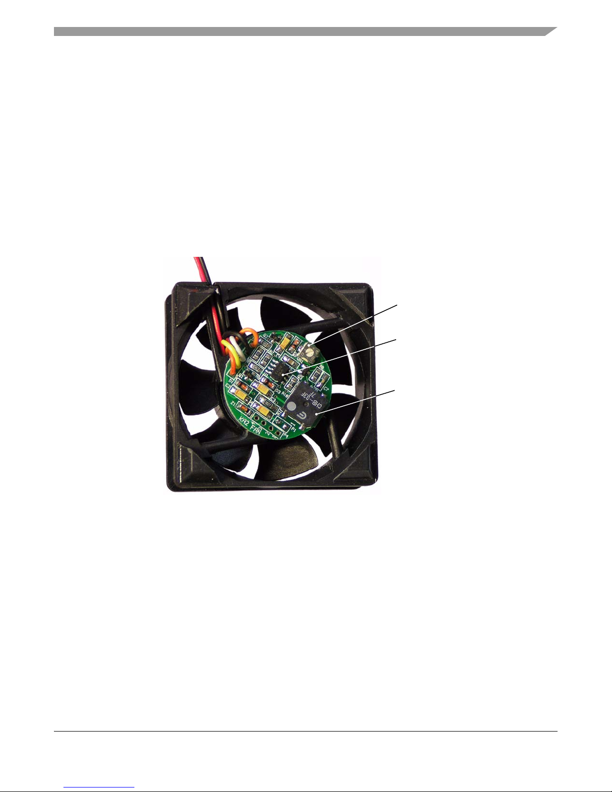
This document describes the implementation of a DC brushless fan controller using the Freescale ultra
low cost MC9RS08KA2 8-bit microcontroller (MCU). The design contains a temperature sensor the MCU
reads with control on fan speed against the ambient temperature. Complete coding and schematic are
included.
VARIABLE RESISTOR
(TO EMULATE A TEMPERATURE SENSOR)
MC9RS08KA2
MCU IN 8-PIN NARROW BODY
SOIC PACKAGE
BUZZER
Figure 1-1. The MC9RS08KA2 DC Fan Reference Design
The DC fan used is a brushless DC motor fan. It is widely used in chip cooling or system ventilation
applications. In the market, most of the DC fans are of the constant air flow design. As the high
performance electronic products continue to increase, cooling requirement becomes more and more
sophisticated. MCU approach provides a cost effective solution to this application. There are several
advantages of a MCU based design over traditional solutions.
1. Instead of having a constant air flow the MCU provides enough processing power to modify the fan
speed according to environment changes such as the temperature of the target system.
2. Fault detection can easily be implemented by the MCU. For example, the MCU can detect for the
air flow blocking or motor jam, the motor driver can be stopped completely to avoid further damage.
3. Buzzer alarm or digital output acknowledgement can be generated under the faulty situation.
The MCU chosen for this purpose must be low cost and it must provide small geometry package to
integrate into the fan controller printed circuit board (PCB). The MC9RS08KA2 is ideal for this application.
Variable Speed DC Fan Control using the MC9RS08KA2, Rev. 0
Freescale Semiconductor 7
Page 8

Introduction
1.2 Freescale’s New Generation Ultra Low Cost MCU
The MC9RS08KA2 microcontroller unit (MCU) is an extremely low cost, small pin count device for home
appliances, toys, and small geometry applications, such as a DC fan controller. This device is composed
of standard on-chip modules including a very small and highly efficient RS08 CPU core, 62 bytes RAM,
2K bytes FLASH, an 8-bit modulo timer, keyboard interrupt, and analog comparator. The device is
available in small 6- and 8-pin packages.
Features of the MC9RS08KA2 include:
• 8-bit RS08 core
– Up to 10 MHz (bus frequency) at 1.8V for 100 ns minimum instruction time
– RS08 instruction set
– Supports tiny/short address mode
– 14-byte fast-access RAM
– Allows emulation of HC08/HCS08 zero-offset index addressing mode instructions
• Third-generation Flash and RAM (extremely fast, byte writable programming)
– 63 Byte RAM
– 2K Byte Flash
• Flexible clock options
• 4 Bidirectional I/O lines with software selectable pull-up (eliminates need for external resistors)
• Analog comparator
• Real time interrupt
• 8-bit timer with 8-bit prescale
• System protection
– Resets in instance of runaways or corrupted code
– Low voltage detection
– Illegal opcode and illegal address detection
– Flash security feature
• Single wire debugging and emulation interface; eliminates need for expensive emulation tools or
development hardware
1.3 DC Fan Reference Design Targets
Table 1-1. Design Targets
Item Requirement
Motor Type Bi-phase BLDC motor
Fan Dimensions 60mm x 60mm x 25mm
Operating Voltage 12V
Current Rating 0.18A (max.)
Speed 1000 to 4000 RPM
Temperature Feedback Yes
Fault Detection Air flow blocking (motor jam)
Fault Notification Buzzer alarm
Variable Speed DC Fan Control using the MC9RS08KA2, Rev. 0
8 Freescale Semiconductor
Page 9
Bi-Phase BLDC Motor
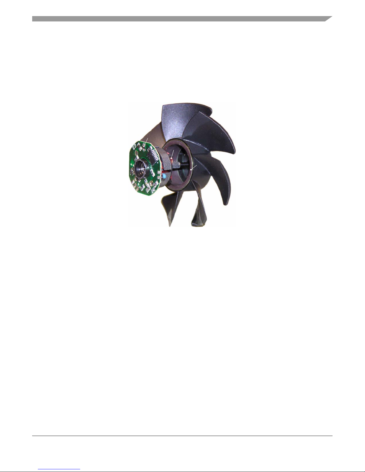
1.4 Bi-Phase BLDC Motor
The brushless DC motor (BLDC) design for DC fan is commonly consist of a permanent magnet attached
on the rotor and the stator phase coil windings are mounted on the motor shaft as illustrated in Figure 1-2.
The BLDC has no brushes on the rotor and the commutation is performed electronically at certain rotor
positions.
Hall Effect
Sensor
Stator
Coil
Fan Hub
Axle
Permanent
Magnets
Figure 1-2. Bi-Phase BLDC Motor Diagram
Variable Speed DC Fan Control using the MC9RS08KA2, Rev. 0
Freescale Semiconductor 9
Page 10

Introduction
Variable Speed DC Fan Control using the MC9RS08KA2, Rev. 0
10 Freescale Semiconductor
Page 11
Commutation
Chapter 2
Motor Control
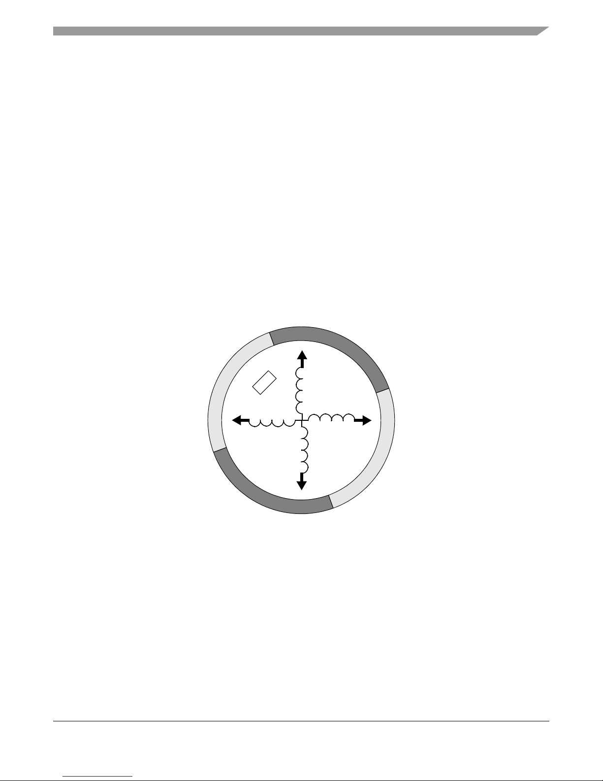
2.1 Commutation
The typical bi-phase BLDC has one pole-pair per phase. Each commutation rotates the rotor by 90
degrees and four commutation steps complete a mechanical revolution. Each pole-pair is implemented
by two coils, with four coils in total for a bi-phase motor. Energizing a pair of coils, either coil A & C or coil
B & D as shown in Figure 2-1, induces magnetic fields that push the equal polarity rotor magnets away
from the energized coils and at the same time the opposite polarity rotor magnets are pulled toward the
coils. Rotation starts and this is called a commutation step. When the rotor magnetic pole is aligned with
the energized coils, the coils are deactivated and the previously un-energized pair of coils are then
energized. As the magnetic field switches to the next motor position or pole, the inertia of the rotor keeps
the motor running. As a result, two commutation steps moves the rotor by 180 degrees or one motor
phase. One mechanical revolution is contributed by four commutation steps.
To avoid conflict to the magnetic field, adjacent coils cannot be energized at the same time. Dead-time,
where all coils are un-energized must be added between each commutation step.
N
L2
S
L1
HALL
Coil A
Coil D
Coil B
L1
Coil C
S
L2
N
Figure 2-1. Bi-phase BLDC Motor Schematic
2.2 Rotor Position Control
The key idea to prevent a motor lockup concerns rotor position detection. The time to switch the
commutation is critical. Energizing coil-pair for too long will kill the rotor inertia and the motor stops
running. This is called motor lockup. Switching the commutation too soon will lose control to the rotor and
eventually stall the motor. The rotor position in this design is determined by a hall sensor which will
respond to the change in magnetic field. Hall sensor output toggles when the magnetic field changes its
polarity. Positioning the hall sensor between the coils at 45 degree to the stator coils, as shown in
Figure 2-1, can effectively detect the rotor position. In this case the hall sensor output toggles when the
rotor magnets is aligned to the coils. Commutation should switch at this time from one coil-pair to the next
coil-pair.
Variable Speed DC Fan Control using the MC9RS08KA2, Rev. 0
Freescale Semiconductor 11
Page 12
Motor Control
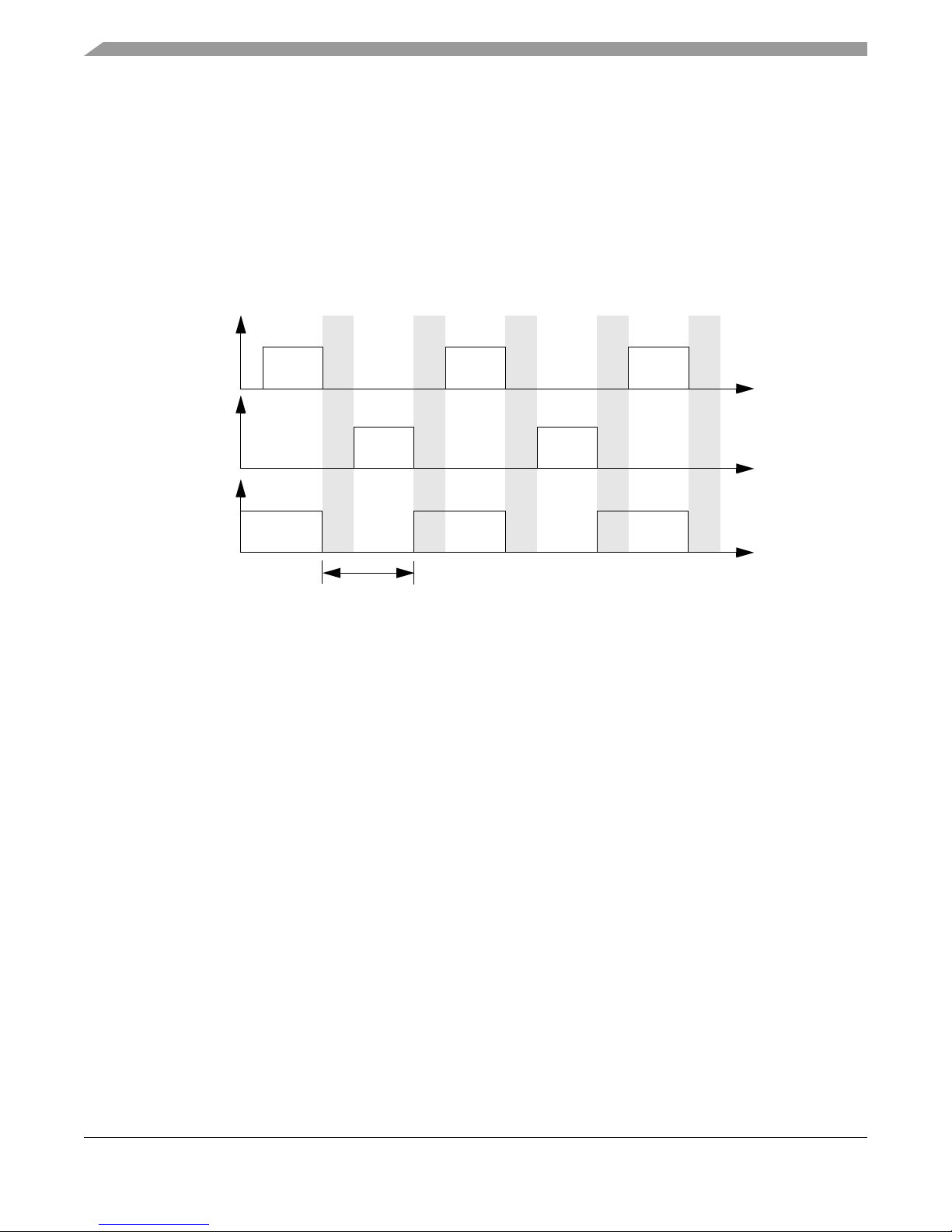
2.3 Commutation Waveforms
In general, in a bi-phase motor design, alternate coils are tied together and give a single connection to
the driver. In this design, the driver connection for coil A and coil C is called L1 (see Figure 2-1). Similarly,
the driver connection for coil B and coil D is called L2. Driving to either of the connections will energize a
coil-pair. The commutation waveform is shown in Figure 2-2. The coil driving period is aligned with the
Hall sensor output. When the sensor output toggles, coil driving is stopped, the coils are de-energized for
a period of time before the next coil-pair is energized.
Dead
Zone
L1
L2
Hall
Output
90° of rotation
Dead
Zone
Dead
Zone
Dead
Zone
Dead
Zone
t
t
t
Figure 2-2. Bi-Phase BLDC Motor Commutation Waveform
2.4 Speed Control
Motor speed is normally defined as the mechanical revolution per one minute of time (rpm). In electrical
terms, one commutation contributes to 90 degrees of a revolution. Thus, control the time taken per
commutation can effectively control the overall speed. One commutation step includes a dead-time
(where the coils are not energized) and the coils energization time. The whole commutation period could
be considered as a pulse width modulation (PWM) output cycle. The PWM period defines the motor speed
in this case. The coils energization time is, in fact, the PWM driving period which is defined by the time
that the coils are energized until the Hall sensor is toggled. The Hall sensor output indicates the position
of the rotor and defines the time to switch to the next commutation step.
In this design the motor speed or the PWM period is continuously monitored. It is a closed-loop control
design. If the motor speed is faster (PWM period is shorter) than the target value, the dead-time duration
is extended until the target PWM period is reached. Similarly, when the motor speed is slower than the
target value, the dead-time duration is shortened.
The rotor starts off at the slowest speed. Shortening the dead-time causes the coils to energize earlier
and the rotor is pushed/pulled to the next pole position sooner, causing motor speed to increase. Similarly,
when the dead-time is extended the rotor hangs loose for a longer time before it is pushed/pulled to the
next pole position. As a result the motor speed decreases. The target motor speed against temperature
is predefined. It is updated periodically based on the information from the temperature sensor.
Variable Speed DC Fan Control using the MC9RS08KA2, Rev. 0
12 Freescale Semiconductor
Page 13

Motor Startup
Dramatic changes in the dead-time value will cause the motor to stall. In this design a software loop in the
MCU will control the dead-time variation. Even with the dramatic change in the temperature sensor
reading, the software loop will only allow the dead-time to change to the new value gradually.
2.5 Motor Startup
In this DC fan application, it is desirable to only allow the motor to operate in an uni-direction, such that
the airflow to the target system will always be in one direction. With the bi-phase motor design it is difficult
to guarantee the direction of rotation. Commutation order or the coil energizing sequence happens to be
the same for both directions of rotation. The rotor position or axis must initially be known in order to
guarantee the direction of rotation. When the first commutation step is activated where the adjacent
coil-pair to the initial axis is energized, the rotor starts to move. Since the adjacent coil-pairs are
connected together and energized at the same time, there are equal pulling/pushing force induced on the
rotor in both directions. There is chance for the rotor to startup in either direction. It is necessary to monitor
the initial direction of rotation. If the direction is not correct, the motor must be locked back to the startup
axis again and the commutation step repeated. The direction of rotation can be detected by the Hall
sensor output. If the initial rotor axis is known, the output edge polarity, rising edge or falling edge,
determines the direction of rotation.
In the modern bi-phase motor design the direction of rotation is normally defined by the manufacturer. The
stator design is not symmetric such that the motor will have a high tendency to rotate in one direction than
the other. However, the direction of rotation cannot be guaranteed without proper monitoring techniques
in place.
2.6 Fault Detection
Motor fault is identified as the rotor not moving, which is normally the case when the rotor is jammed (may
be cause by blocked airflow). During each commutation step, the Hall sensor output is monitored. If it is
not toggled within a defined duration, commutation sequence is terminated, all coils are de-energized. In
this design, when a motor fault occurs, a buzzer is activated as the alarm.
Variable Speed DC Fan Control using the MC9RS08KA2, Rev. 0
Freescale Semiconductor 13
Page 14

Motor Control
Variable Speed DC Fan Control using the MC9RS08KA2, Rev. 0
14 Freescale Semiconductor
Page 15

Block Diagram
Chapter 3
Implementation
3.1 Block Diagram
The block diagram of the DC fan design is illustrated in Figure 3-1. A 12V low cost bi-phase BLDC motor
is used in this application. The MCU performs alternate outputs to the two NPN transistors that drive the
motor coils. Open drain output Hall sensor is required and positioned close the rotor. The device responds
to magnetic field changes during the motor operation, digitizing output feedback of the rotor position to
the MCU for close loop motor control and fault detection. Ambient temperature information is measured
from an external temperature sensor. In the faulty situation, such as motor jam, the buzzer alarm is driven
by the MCU through a pulse width modulated (PWM) output.
L1
L2
VOLTAGE
REGULATION
HALL
PTA2
PTA4
PTA5
VDD
MC9RS08KA2
PTA3
ACMP+
+
ACMP–
–
BUZZER
RC
TEMP
SENSOR
12V
BI-PHASE
MOTOR
Figure 3-1. DC Fan Design Block Diagram
3.2 Hardware Resources
In this application, the low cost MC9RS08KA2 MCU is used. The device has a built-in 8-bit modulo timer
which is used to control the timing for the PWM drive. Bus frequency is chosen to be 4MHz. The design
target for the maximum motor speed is 4000 rpm, the timer must have enough resolution to measure the
shortest PWM period that is less the 3.75ms per commutation step. Timer prescalar is selected as 256
and the timer resolution becomes 64µs.
Timer Clock for motor speed monitoring 4MHz/256 = 16kHz
Variable Speed DC Fan Control using the MC9RS08KA2, Rev. 0
Freescale Semiconductor 15
Table 3-1. Hardware Configuration
Bus Frequency 4MHz
Timer Resolution 64µs
Page 16

Implementation
Hall sensor output is connected to the MCU’s GPIO port, PTA2, which has a programmable edge trigger
keyboard interrupt (KBI). The programmable edge trigger feature provides an effective way to monitor the
Hall sensor signal. As mentioned in the previous section, the direction of rotation can be detected by the
polarity of the Hall sensor output edge. Monitoring the signal edge is achieved by altering the KBI edge
trigger polarity for each commutation step.
Ambient temperature reading is taken from a temperature sensor which is equivalent to a diode.
Temperature variation alters the diode channel current as well as the effective channel resistance. The
temperature sensor is combined with a 7.5kΩ resistor in a potential divider arrangement. The built-in
analog comparator is used to compare the temperature sensor ladder voltage with an defined RC network
to deduce the absolute temperature.
As described in the previous section, the motor speed is controlled by varying the absolute dead-time.
This is updated every 128ms in the application. As in all RS08/S08 devices, the MC9RS08KA2 MCU has
a programmable real time interrupt (RTI) feature. In this case, it is used to notify the MCU to refresh the
target PWM period every 128ms.
3.3 Control Loop
Figure 3-2 shows the firmware control loop flow chart. The KBI or Hall sensor output is continuously
monitored for trigger signals within a defined time. A motor fault condition occurs when there are no trigger
signal, and the firmware goes into a forever loop. Commutation is stopped and the buzzer is alarmed.
The target PWM period based on the temperature sensor reading is updated every 128ms. And on each
180 degrees rotation of the rotor (two commutation steps) the actual PWM period is compared with the
target PWM period. If they are different, the absolute dead-time will be altered, and the actual PWM period
will gradually change towards the target PWM period.
On each commutation step, reading of the temperature sensor contributes a delay to the actual dead-time
duration. This delay is deterministic such that the software control loop can easily deduce the actual
speed of the motor. Hence, this delay can be considered as a part of the total dead-time delay for each
commutation.
Variable Speed DC Fan Control using the MC9RS08KA2, Rev. 0
16 Freescale Semiconductor
Page 17

START
Control Loop
TargetPWMPeriod = Longest
ActualPWMPeriod = Longest
Drive L1
Read Temp. Sensor
De-energized coils = DeadTime
Drive L2
Read Temp. Sensor
De-energized coils = DeadTime
During the dead time delay update PWM period for the next commutation
Continuously monitor the hall sensor output
Energize L1 / L2
Start Timer
Hall
Edge?
Y
Stop Timer
N
Timeout?
Y
De-energize Coils
Record DriveTime
Sound Buzzer
De-energize Coils
ActualPWMPeriod =
DriveTime + DeadTime
N
Fault
condition
detected.
128ms?
Y
Update TargetPWMPeriod
Target >
Actual?
Y
N
Modify Target PWM period value
every 128ms based on temperature
reading
N
Target =
Actual?
Y
Increment DeadTime
Figure 3-2. Firmware Control Loop
N
Decrement DeadTime
Variable Speed DC Fan Control using the MC9RS08KA2, Rev. 0
Freescale Semiconductor 17
Page 18

Implementation
3.4 Temperature Sensor Measurement
The temperature sensor measurement is performed based on the methodology of an emulated ADC
described in the application note, AN3266 “Getting Started with RS08”.
V
DD
ON-CHIP
COMPARATOR
+
–
MCU BOUNDARY
R
4k7
C
22nF
Figure 3-3. Emulated ADC Schematic
The schematic of the emulated ADC in this application is shown in Figure 3-3. The ADC input is the
temperature sensor resistor ladder. When the comparator is not measuring, the capacitor, C, is fully
discharged where the positive terminal of the comparator is pulling low. When the temperature sensor
measurement is required, the comparator is then enabled and the terminal turns to analog input, voltage
across C starts to ramp up. The 8-bit internal modulo timer is used to monitor the time taken for the RC
to charge to a level that matches the voltage across the temperature sensor. The timer counter value is
captured and used as the basis for the emulated ADC conversion.
V
DD
7k5
TEMP SENSOR
10k
With a 10kΩ temperature sensor and 7.5kΩ pullup resistor the ADC absolute dynamic range is from 0V
to about 0.57 × V
, i.e. about 2.85V. Timer clock is chosen to be eight times slower than the bus clock,
DD
the timer resolution becomes 2µs. The RC charging profile follows EQ 3-1. Given the RC constant is
4K7Ω × 22nF the timer counter value against the temperature sensor reading with 5V V
is shown in
DD
Table 3-2.
t
--------–
⎛⎞
VVDD1e
=
RC
–
⎜⎟
⎝⎠
(EQ 3-1)
Variable Speed DC Fan Control using the MC9RS08KA2, Rev. 0
18 Freescale Semiconductor
Page 19

Temperature Sensor Measurement
Table 3-2. RC Charging Profile Against Timer Count
Time (µs)
00 0
20.10 1
40.19 2
60.28 3
86 2.82 43
88 2.87 44
90 2.91 45
126 3.52 63
Voltage across the
Temperature Sensor (V)
and so on...
and so on...
ADC Readout
(Timer Count)
Table 3-2 shows the entire dynamic range of the temperature sensor voltage can be covered by about 44
timer counts. For convenience, the timer overflow period is set to 63, which is identical to the size of the
paging window ($00C0 to $00FF) in the MC9RS08KA2. The timer value captured can be used directly as
an index to the paging window for the target PWM period value lookup.
The code below shows how the timer value is captured using RS08 instructions.
ReadSensor:
mov #(MTIM_BUS_CLK|MTIM_DIV_8), MTIMCLK; Change Timer resolution
mov #63, MTIMMOD ; OF period
mov #(mMTIMSC_TRST|mMTIMSC_TOIE), MTIMSC; Reset and Start Timer
mov #(mACMPSC_ACME|mACMPSC_ACIE|ACMP_OUTPUT_RAISING), ACMPSC
bset ACMPSC_ACF, ACMPSC ; Clear ACMP Flag
wait
brclr ACMPSC_ACF, ACMPSC, NoReading
mov MTIMCNT, SensorReading ; Capture timer count
bset ACMPSC_ACF, ACMPSC ; Clear ACMP Flag
clr ACMPSC ; disable ACMP
wait ; delay to OF and make the
mov #(mMTIMSC_TSTP|mMTIMSC_TRST), MTIMSC; mask interrupt and clear
mov #(MTIM_BUS_CLK|MTIM_DIV_256), MTIMCLK; Reset Timer resolution
rts
NoReading:
mov #$00, SensorReading ; Smallest Number
clr ACMPSC ; disable ACMP
mov #(mMTIMSC_TSTP|mMTIMSC_TRST), MTIMSC ; mask interrupt and clear
mov #(MTIM_BUS_CLK|MTIM_DIV_256), MTIMCLK; Reset Timer resolution
rts
; Enable ACMP, start RC rise
; read process deterministic
; flag
; flag
Variable Speed DC Fan Control using the MC9RS08KA2, Rev. 0
Freescale Semiconductor 19
Page 20

Implementation
As described in the previous section the overall dead-time duration should be deterministic, the double
WAIT statements in the subroutine can ensure the execution time to be mostly constant. When the MCU
is woken up from the first WAIT (which is normally triggered by the comparator), the timer counter value
is captured and the MCU is then returned to WAIT mode until the timer is overflowed. The subroutine
execution time would be equivalent to the timer overflow period (~128µs) plus some software overhead.
3.4.1 Temperature Conversion
In general, the channel resistance of the temperature sensor reduces as the temperature increases. The
corresponding channel resistance against temperature can usually be retrieved from the sensor data
sheet. For this application the operating temperature range is defined from 25°C to 100°C. When the
ambient temperature is 100°C or above the motor is at maximum speed. The speed drops as the
temperature decreases in 5°C steps. Given the sensor channel resistance values the voltage across the
sensor can be calculated. The corresponding motor speed for a specific temperature range are also
defined and shown in Table 3-3.
EQ 3-2 shows how the target PWM period value is calculated. The target value is compared with the
measured PWM period every 180 degrees of rotation. The ADC readout delay is considered as constant,
therefore, it is omitted from the motor speed measurement and should be deducted from the target period
calculation, too.
60 RPM⁄
---------------------- A D C D e l a y–
TetPWMPeriodarg
4
--------------------------------------------------------- -=
TimerResolution
(EQ 3-2)
The timer resolution used in the application is 64µs, the ADC readout time contributes a constant delay
to the overall PWM period, which is ~128µs in this application. The target PWM period used for motor
speed control is shown in Table 3-3. The table is stored in the upper memory (FLASH). In RS08
architecture upper memory access is done through the paging window (address $00C0 to $00FF) where
the PAGESEL register is defining the page to be accessed. Simple table lookup method which uses the
captured timer value from the temperature sensor readout as an index in the paging window for the target
PWM period conversion.
For software implementation, the target motor speed must be deduced in terms of timer counts, where it
is used as the target PWM period per commutation. By using Table 3-2 and Table 3-3, a look-up table
can be constructed where the ADC readout value is used as an index to retrieve the target PWM period
for a specific temperature range.
Variable Speed DC Fan Control using the MC9RS08KA2, Rev. 0
20 Freescale Semiconductor
Page 21

Table 3-3. Temperature Conversion Table
Temperature Sensor Measurement
Temperature
(°C)
25 or below 10 2.86 1000 232
30 – 34 8.082 2.59 1200 193
35 – 39 6.577 2.34 1400 165
40 – 44 5.387 2.09 1600 144
45 – 49 4.441 1.86 1800 128
50 – 54 3.683 1.65 2000 115
55 – 59 3.024 1.44 2200 105
60 – 64 2.53 1.26 2400 96
65 – 69 2.128 1.11 2600 88
70 – 74 1.799 0.97 2800 82
75 – 79 1.528 0.85 3000 76
80 – 84 1.304 0.74 3200 71
85 – 89 1.118 0.65 3400 67
Channel Resistance
(kΩ)
(from sensor data sheet)
Voltage
across
Sensor
(V)
Predefined
Motor Speed
(rpm)
Target PWM Period
(Timer Counts
(1)
)
90 – 94 0.962 0.57 3600 63
95 – 99 0.831 0.50 3800 60
100 or above 0.698 0.43 4000 57
NOTES:
1. The resolution of a timer count is 64µs.
Variable Speed DC Fan Control using the MC9RS08KA2, Rev. 0
Freescale Semiconductor 21
Page 22

Implementation
Variable Speed DC Fan Control using the MC9RS08KA2, Rev. 0
22 Freescale Semiconductor
Page 23

Appendix A.
Schematic
BUZ1
1
2
12V
Temperature Sensor Measurement
Q3
NDS7002A
2
3
1
GND
5V
4K7(1%)
R10
1
2
C7
22nF
1
2
GND
5V
R9
7.5K(1%)
1
2
10K
1
2
GND
3
VR1
VPP
BKGD
123
HALL
BUZZER
D3
LL4148
C3
SPEED CONTROL
5V
GND
4
5V
GND
2
2u2F/25V
ICP CONNECTOR
GND
1K5
R8
12
OUT1
OUT2
SENSOR
678
PA4/K4
PA1/K1/A-
PA0/K0/A+
U1
DC1
5V
1K5
1
C6
12
Z1
2
1uF/10V
ZMM5231B
5V
2
220
R1
1
R6
3
D2
12
12
LL4148
1
FMMT491A
2
Q2
1
2
GND
1
9RS08KA2DN
PA3/AO/BKGD
PA2/K2/RST
VDD
VSS PA5/K5
123
45
5V
GND
HALL
BUZZER
0.1uF
GND
2
3
P4
1K5
R7
12
12
1
FMMT491A
2
Q1
1
C4
2u2F/25V
D1
LL4148
12
P1
12V_IN
1
2
GND
12V
12V
GND
1
C2
Variable Speed DC Fan Control using the MC9RS08KA2, Rev. 0
Freescale Semiconductor 23
2
2u2F/25V
10K
5V
GND
R2
1
12V
2
12V
12345
P3
COM
L2
L1
L2
L1
GND
HALL
GND
GND
HALL
BLDC FAN CONNECTOR
Page 24

Implementation
Variable Speed DC Fan Control using the MC9RS08KA2, Rev. 0
24 Freescale Semiconductor
Page 25

Temperature Sensor Measurement
Appendix B.
Program Listing
;**************************************************************
;
; (c) copyright Freescale Semiconductor. 2006
; ALL RIGHTS RESERVED
;
;**************************************************************
;**************************************************************
;* DC Fan Coding for 9RS08KA2
;*
;* Author: Vincent Ko
;* Date: Jan 2006
;*
;* PTA0/KBI0/ACMP+ RC input
;* PTA1/KBI1/ACMP- Temp sensor input
;* PTA2/KBI2/TCLK/RESETb/VPP Hall input
;* PTA3/ACMPO/BKGD/MS Buzzer
;* PTA4/KBI4 PWM+
;* PTA5/KBI5 PWM;*
;**************************************************************
; include derivative specific macros
XDEF Entry
include "MC9RS08KA2.inc"
;=========================================================================
; ICS Definition
;=========================================================================
ICS_DIV_1 equ$00
ICS_DIV_2 equ$40
ICS_DIV_4 equ$80
ICS_DIV_8 equ$c0
;=========================================================================
; MTIM Definition
;=========================================================================
MTIM_DIV_1 equ $00
MTIM_DIV_2 equ $01
MTIM_DIV_4 equ $02
MTIM_DIV_8 equ $03
MTIM_DIV_16 equ $04
MTIM_DIV_32 equ $05
MTIM_DIV_64 equ $06
MTIM_DIV_128 equ $07
MTIM_DIV_256 equ $08
MTIM_BUS_CLK equ $00
MTIM_XCLK equ $10
Variable Speed DC Fan Control using the MC9RS08KA2, Rev. 0
Freescale Semiconductor 25
Page 26

Implementation
MTIM_TCLK_FALLING equ $20
MTIM_TCLK_RISING equ $30
;=========================================================================
; ACMP Definition
;=========================================================================
ACMP_OUTPUT_FALLING equ $00
ACMP_OUTPUT_RAISING equ $01
ACMP_OUTPUT_BOTH equ $03
;=========================================================================
; RTI Definition
;=========================================================================
RTI_DISABLE equ $00
RTI_8MS equ $01
RTI_32MS equ $02
RTI_64MS equ $03
RTI_128MS equ $04
RTI_256MS equ $05
RTI_512MS equ $06
RTI_1024MS equ $07
;=========================================================================
; Application Definition
;=========================================================================
RC equ PTAD_PTAD0
mRC equ mPTAD_PTAD0
TEMPSEN equ PTAD_PTAD1
mTEMPSEN equ mPTAD_PTAD1
HALL equ PTAD_PTAD2
mHALL equ mPTAD_PTAD2
BUZZER equ PTAD_PTAD3
mBUZZER equ mPTAD_PTAD3
PWM2 equ PTAD_PTAD4
mPWM2 equ mPTAD_PTAD4
PWM1 equ PTAD_PTAD5
mPWM1 equ mPTAD_PTAD5
MinDeadTime equ 2
MaxDeadTime equ 150
TableStart: equ $00003E00
;=========================================================================
; Application Macro
;=========================================================================
StartTimer: macro
mov DeadTime, MTIMMOD ; OF period
mov #(mMTIMSC_TRST|mMTIMSC_TOIE), MTIMSC; Reset and Start Timer
endm
org TINY_RAMStart
; variable/data section
DeadTime ds.b 1
Variable Speed DC Fan Control using the MC9RS08KA2, Rev. 0
26 Freescale Semiconductor
Page 27

TargetPeriod ds.b 1
ActualPeriod ds.b 1
DriveTime ds.b 1
SensorReading ds.b 1
MotorRunning ds.b 1
org RAMStart
; variable/data section
org ROMStart
; code section
main:
Entry:
;------------------------------------------------------; Config ICS
; Device is pre-trim to 16MHz ICLK frequency
; TRIM value are stored in $3FFA:$3FFB
;-------------------------------------------------------
mov #HIGH_6_13(NV_ICSTRM), PAGESEL
mov MAP_ADDR_6(NV_FTRIM), ICSSC ; $3FFB
mov MAP_ADDR_6(NV_ICSTRM), ICSTRM ; $3FFA
mov #ICS_DIV_2, ICSC2 ; Use 4MHz
Temperature Sensor Measurement
;------------------------------------------------------;Config System
;-------------------------------------------------------
mov #HIGH_6_13(SOPT), PAGESEL ; Init Page register
mov #(mSOPT_COPT|mSOPT_STOPE), MAP_ADDR_6(SOPT)
; BKGD disable, COP disabled
mov #(mSPMSC1_LVDE|mSPMSC1_LVDRE), MAP_ADDR_6(SPMSC1); LVI enable
mov #(RTI_128MS), MAP_ADDR_6(SRTISC) ; 128ms RTI
;------------------------------------------------------; Init RAM
;-------------------------------------------------------
mov #MaxDeadTime, DeadTime
mov #232, TargetPeriod ; 1000 rpm
mov #232, ActualPeriod ; 1000 rpm
clr SensorReading
clr MotorRunning
;------------------------------------------------------; Config GPIO
; RC - init L
; Buzzer - init L
; PWMn/PWMp - init L
;-------------------------------------------------------
clr PTAD ; Initial low
mov #(mRC|mPWM1|mPWM2), PTADD ; Set Output pins
;------------------------------------------------------; Config KBI
;-------------------------------------------------------
lda #mHALL
Variable Speed DC Fan Control using the MC9RS08KA2, Rev. 0
Freescale Semiconductor 27
Page 28

Implementation
sta KBIES ;HALL rising Edge Trigger
sta KBIPE ;KBI Enable
;------------------------------------------------------;Config MTIM
;
;Timer prescalar=256 -> Timer clk = 16kHz
;Bus = 4MHz
;Max OF period = 16.384ms
;Timer resolution = 64us
;-------------------------------------------------------
mov #(MTIM_BUS_CLK|MTIM_DIV_256), MTIMCLK
mov #255, MTIMMOD
;------------------------------------------------------;Motor Start Sequence
;------------------------------------------------------ResetPosition:
mov #mPWM1, PTAD ; Lock FAN in reset position
lda #30 ;
Dly1 bsr Delay ; for Delay 0.5s
dbnza Dly1 ;
clr PTAD ; de-energize coils
bsr Delay
; Drive L2
ldx #mPWM2 ; Select L2 Coils
bsr SetPWM ; Drive coil
bsr Delay ; De-energize coils
inc MotorRunning ; otherwise Update Software flag
;------------------------------------------------------;Fan Control Loop
;------------------------------------------------------FanControlLoop:
;1) Drive L1 coil
clr KBIES ; HALL falling edge trigger
ldx #mPWM1 ; Select L1 Coil
bsr SetPWM ; Drive coil
;2) Read Temp Sensor
jsr ReadSensor ; Read Sensor value
;3) Dead time control
StartTimer ; Wait dead time period
wait
mov #(mMTIMSC_TSTP|mMTIMSC_TRST), MTIMSC; mask interrupt and clear flag
;4) Drive L2 coil
bset HALL, KBIES ; HALL rising edge trigger
ldx #mPWM2 ; Select L2 Coil
bsr SetPWM ; Drive coil
Variable Speed DC Fan Control using the MC9RS08KA2, Rev. 0
28 Freescale Semiconductor
Page 29

Temperature Sensor Measurement
;5) Read Temp Sensor Again
bsr ReadSensor ; Read Sensor value
;6) Dead time control
StartTimer
;7) During the dead time, update dead time period every 128ms
brclr SRTISC_RTIF, MAP_ADDR_6(SRTISC), UpdateLater; Update PWM duty cycle
jsr TableLookup
UpdateLater:
lda ActualPeriod
sub TargetPeriod ; Actual-Target
blo IncPeriod
beq WaitAgain ; if same, Fan speed reach target then exit
DecPeriod: ; if bigger, decrement DeadTime
lda DeadTime
cmp #MinDeadTime
blo WaitAgain
dec DeadTime
bra WaitAgain
IncPeriod: ; if smaller, increment DeadTime
lda DeadTime
cmp #MaxDeadTime
bhs WaitAgain
inc DeadTime
bra WaitAgain
WaitAgain:
;8) Bump COP
sta MAP_ADDR_6(SRS) ; Bump COP
wait
mov #(mMTIMSC_TSTP|mMTIMSC_TRST), MTIMSC; mask interrupt and clear flag
;9) Repeat the control cycle
bra FanControlLoop
;%%%%%%%%%%%%%%%%%%%%%%%%%%%%%%%%%%%%%%%%%%%%%%%%%%%%%%%%%%%%%%%%%%%%%%%%%%%
; Delay 16ms
;%%%%%%%%%%%%%%%%%%%%%%%%%%%%%%%%%%%%%%%%%%%%%%%%%%%%%%%%%%%%%%%%%%%%%%%%%%%
Delay:
mov #255, MTIMMOD ; OF period
mov #(mMTIMSC_TRST|mMTIMSC_TOIE), MTIMSC; Reset and Start Timer
wait
mov #(mMTIMSC_TSTP|mMTIMSC_TRST), MTIMSC; mask interrupt and clear flag
sta MAP_ADDR_6(SRS) ; Bump COP
rts
;%%%%%%%%%%%%%%%%%%%%%%%%%%%%%%%%%%%%%%%%%%%%%%%%%%%%%%%%%%%%%%%%%%%%%%%%%%%
; Drive coil
;
Variable Speed DC Fan Control using the MC9RS08KA2, Rev. 0
Freescale Semiconductor 29
Page 30

Implementation
; X indicate the coil to be driven
;%%%%%%%%%%%%%%%%%%%%%%%%%%%%%%%%%%%%%%%%%%%%%%%%%%%%%%%%%%%%%%%%%%%%%%%%%%%
SetPWM:
mov #255, MTIMMOD ; OF period
mov #(mMTIMSC_TRST|mMTIMSC_TOIE), MTIMSC; Reset and Start Timer
lda #20
mov #(mKBISC_KBIE), KBISC ; Enable Interrupt & Edge only
bset KBISC_KBACK, KBISC ; Clear Flag
stx PTAD ; Drive coil
TimingLoop:
bclr MTIMSC_TOF, MTIMSC ; Clear TOF
wait
brset KBISC_KBF, KBISC, HallFound ; HALL sensor edge found
dbnza TimingLoop
jmp MotorHang ; If no HALL output, Stop the driving
HallFound:
mov MTIMCNT, DriveTime
cbeqa #20, StableDrive
mov #MaxDeadTime, DriveTime
StableDrive:
lda DeadTime
add DriveTime
sta ActualPeriod
clr PTAD ; Disconnect coil
mov #(mKBISC_KBACK), KBISC ; Clear Flag and mask interrupt
mov #(mMTIMSC_TSTP|mMTIMSC_TRST), MTIMSC; mask interrupt and clear flag
rts
;%%%%%%%%%%%%%%%%%%%%%%%%%%%%%%%%%%%%%%%%%%%%%%%%%%%%%%%%%%%%%%%%%%%%%%%%%%%
; Read Temperature Sensor Value
; Timer prescalar=8 -> Timer clk~250kHz
; Bus = 2MHz
; Max OF period = 1.02ms
; Timer resolution = 4us
;%%%%%%%%%%%%%%%%%%%%%%%%%%%%%%%%%%%%%%%%%%%%%%%%%%%%%%%%%%%%%%%%%%%%%%%%%%%
ReadSensor:
mov #(MTIM_BUS_CLK|MTIM_DIV_8), MTIMCLK; Change Timer resolution
mov #63, MTIMMOD ; OF period
mov #(mMTIMSC_TRST|mMTIMSC_TOIE), MTIMSC; Reset and Start Timer
mov #(mACMPSC_ACME|mACMPSC_ACIE|ACMP_OUTPUT_RAISING), ACMPSC
; Enable ACMP, start RC rise
bset ACMPSC_ACF, ACMPSC ; Clear ACMP Flag
wait ; delay to OF and make the read process deterministic
brclr ACMPSC_ACF, ACMPSC, NoReading
mov MTIMCNT, SensorReading
bset ACMPSC_ACF, ACMPSC ; Clear ACMP Flag
clr ACMPSC ; disable ACMP
wait
mov #(mMTIMSC_TSTP|mMTIMSC_TRST), MTIMSC; mask interrupt and clear flag
mov #(MTIM_BUS_CLK|MTIM_DIV_256), MTIMCLK; Reset Timer resolution
rts
Variable Speed DC Fan Control using the MC9RS08KA2, Rev. 0
30 Freescale Semiconductor
Page 31

Temperature Sensor Measurement
NoReading:
mov #$00, SensorReading ; Smallest Number
clr ACMPSC ; disable ACMP
mov #(mMTIMSC_TSTP|mMTIMSC_TRST), MTIMSC ; mask interrupt and clear flag
mov #(MTIM_BUS_CLK|MTIM_DIV_256), MTIMCLK; Reset Timer resolution
rts
;%%%%%%%%%%%%%%%%%%%%%%%%%%%%%%%%%%%%%%%%%%%%%%%%%%%%%%%%%%%%%%%%%%%%%%%%%%%
; 6-bit Table Lookup
;%%%%%%%%%%%%%%%%%%%%%%%%%%%%%%%%%%%%%%%%%%%%%%%%%%%%%%%%%%%%%%%%%%%%%%%%%%%
TableLookup:
bset SRTISC_RTIACK, MAP_ADDR_6(SRTISC);5
mov #HIGH_6_13(TableStart), PAGESEL;5 Calculate the PAGE
lda SensorReading ;3
add #$c0 ;2 Reference to paging window
tax ;2
lda ,x ;3
sta TargetPeriod ;2
mov #HIGH_6_13(SOPT), PAGESEL ;5
rts ;3
;%%%%%%%%%%%%%%%%%%%%%%%%%%%%%%%%%%%%%%%%%%%%%%%%%%%%%%%%%%%%%%%%%%%%%%%%%%%
; Error Handling
; Stop the motor
; Sound the buzzer (about 520Hz)
;%%%%%%%%%%%%%%%%%%%%%%%%%%%%%%%%%%%%%%%%%%%%%%%%%%%%%%%%%%%%%%%%%%%%%%%%%%%
MotorHang:
clr PTAD ; clear PWMp and PWMn
lda MotorRunning ; Check software flag
bne SoundBuzzer ; =1, Motor is running
jmp ResetPosition
SoundBuzzer:
mov #(mMTIMSC_TSTP|mMTIMSC_TRST), MTIMSC; mask interrupt and clear flag
clr KBISC ; mask KBI
lda #255
sta MAP_ADDR_6(SRS) ; Bump COP
Beep: ; a 20% duty cycle loop
bset BUZZER, PTAD ; Drive buzzer
mov #6, MTIMMOD
mov #(mMTIMSC_TRST|mMTIMSC_TOIE), MTIMSC; Reset and Start Timer
wait
mov #(mMTIMSC_TSTP|mMTIMSC_TRST), MTIMSC; mask interrupt and clear flag
sta MAP_ADDR_6(SRS) ; Bump COP
bclr BUZZER, PTAD ; Clear buzzer
mov #24, MTIMMOD
mov #(mMTIMSC_TRST|mMTIMSC_TOIE), MTIMSC; Reset and Start Timer
wait
mov #(mMTIMSC_TSTP|mMTIMSC_TRST), MTIMSC; mask interrupt and clear flag
sta MAP_ADDR_6(SRS) ; Bump COP
dbnza Beep
Variable Speed DC Fan Control using the MC9RS08KA2, Rev. 0
Freescale Semiconductor 31
Page 32

Implementation
lda #255
Quiet:
bclr BUZZER, PTAD ; Clear buzzer
mov #30, MTIMMOD
mov #(mMTIMSC_TRST|mMTIMSC_TOIE), MTIMSC; Reset and Start Timer
wait
mov #(mMTIMSC_TSTP|mMTIMSC_TRST), MTIMSC; mask interrupt and clear flag
sta MAP_ADDR_6(SRS) ; Bump COP
dbnza Quiet
bra SoundBuzzer
;%%%%%%%%%%%%%%%%%%%%%%%%%%%%%%%%%%%%%%%%%%%%%%%%%%%%%%%%%%%%%%%%%%%%%%%%%%%
; Lookup Table
;%%%%%%%%%%%%%%%%%%%%%%%%%%%%%%%%%%%%%%%%%%%%%%%%%%%%%%%%%%%%%%%%%%%%%%%%%%%
org TableStart
dc.b 57, 57, 57, 57, 57, 60, 63, 67, 71, 76, 82, 82, 88, 88, 96, 96
dc.b 105,105,115,115,115,128,128,128,128,144,144,144,144,165,165,165
dc.b 165,193,193,193,193,193,232,232,232,232,232,232,232,232,232,232
dc.b 232,232,232,232,232,232,232,232,232,232,232,232,232,232,232,232
;%%%%%%%%%%%%%%%%%%%%%%%%%%%%%%%%%%%%%%%%%%%%%%%%%%%%%%%%%%%%%%%%%%%%%%%%%%%
; Reset Vector
;%%%%%%%%%%%%%%%%%%%%%%%%%%%%%%%%%%%%%%%%%%%%%%%%%%%%%%%%%%%%%%%%%%%%%%%%%%%
org $3ffc
Security:
dc.b $FF
jmp main
Variable Speed DC Fan Control using the MC9RS08KA2, Rev. 0
32 Freescale Semiconductor
Page 33

Page 34

How to Reach Us:
Home Page:
www.freescale.com
E-mail:
support@freescale.com
USA/Europe or Locations Not Listed:
Freescale Semiconductor
Technical Information Center, CH370
1300 N. Alma School Road
Chandler, Arizona 85224
+1-800-521-6274 or +1-480-768-2130
support@freescale.com
Europe, Middle East, and Africa:
Freescale Halbleiter Deutschland GmbH
Technical Information Center
Schatzbogen 7
81829 Muenchen, Germany
+44 1296 380 456 (English)
+46 8 52200080 (English)
+49 89 92103 559 (German)
+33 1 69 35 48 48 (French)
support@freescale.com
Japan:
Freescale Semiconductor Japan Ltd.
Headquarters
ARCO Tower 15F
1-8-1, Shimo-Meguro, Meguro-ku,
Tokyo 153-0064
Japan
0120 191014 or +81 3 5437 9125
support.japan@freescale.com
Asia/Pacific:
Freescale Semiconductor Hong Kong Ltd.
Technical Information Center
2 Dai King Street
Tai Po Industrial Estate
Tai Po, N.T., Hong Kong
+800 2666 8080
support.asia@freescale.com
For Literature Requests Only:
Freescale Semiconductor Literature Distribution Center
P.O. Box 5405
Denver, Colorado 80217
1-800-441-2447 or 303-675-2140
Fax: 303-675-2150
LDCForFreescaleSemiconductor@hibbertgroup.com
RoHS-compliant and/or Pb-free versions of Freescale products have the functionality
and electrical characteristics of their non-RoHS-compliant and/or non-Pb-free
counterparts. For further information, see http://www.freescale.com or contact your
Freescale sales representative.
For information on Freescale’s Environmental Products program, go to
http://www.freescale.com/epp.
Information in this document is provided solely to enable system and software
implementers to use Freescale Semiconductor products. There are no express or
implied copyright licenses granted hereunder to design or fabricate any integrated
circuits or integrated circuits based on the information in this document.
Freescale Semiconductor reserves the right to make changes without further notice to
any products herein. Freescale Semiconductor makes no warranty, representation or
guarantee regarding the suitability of its products for any particular purpose, nor does
Freescale Semiconductor assume any liability arising out of the application or use of any
product or circuit, and specifically disclaims any and all liability, including without
limitation consequential or incidental damages. “Typical” parameters that may be
provided in Freescale Semiconductor data sheets and/or specifications can and do vary
in different applications and actual performance may vary over time. All operating
parameters, including “Typicals”, must be validated for each customer application by
customer’s technical exper ts. Freescale Semiconductor does not convey any license
under its patent rights nor the rights of others. Freescale Semiconductor products are
not designed, intended, or authorized for use as components in systems intended for
surgical implant into the body, or other applications intended to support or sustain life,
or for any other application in which the failure of the Freescale Semiconductor product
could create a situation where personal injury or death may occur. Should Buyer
purchase or use Freescale Semiconductor products for any such unintended or
unauthorized application, Buyer shall indemnify and hold Freescale Semiconductor and
its officers, employees, subsidiaries, affiliates, and distributors harmless against all
claims, costs, damages, and expenses, and reasonable attorney fees arising out of,
directly or indirectly, any claim of personal injury or death associated with such
unintended or unauthorized use, even if such claim alleges that Freescale
Semiconductor was negligent regarding the design or manufacture of the part.
Freescale™ and the Freescale logo are trademarks of Freescale Semiconductor, Inc.
All other product or service names are the property of their respective owners.
© Freescale Semiconductor, Inc. 2006. All rights reserved.
DRM079
Rev. 0, 5/2006
 Loading...