

Page 1

QE128 Quick Reference User Guide
Devices Supported:
MCF51QE128
MC9S08QE128
Document Number: QE128QRUG
Rev. 1.0
10/2007
Page 2

How to Reach Us:
Home Page:
www.freescale.com
E-mail:
support@freescale.com
USA/Europe or Locations Not Listed:
Freescale Semiconductor
Technical Information Center, CH370
1300 N. Alma School Road
Chandler, Arizona 85224
+1-800-521-6274 or +1-480-768-2130
support@freescale.com
Europe, Middle East, and Africa:
Freescale Halbleiter Deutschland GmbH
Technical Information Center
Schatzbogen 7
81829 Muenchen, Germany
+44 1296 380 456 (English)
+46 8 52200080 (English)
+49 89 92103 559 (German)
+33 1 69 35 48 48 (French)
support@freescale.com
Japan:
Freescale Semiconductor Japan Ltd.
Headquarters
ARCO Tower 15F
1-8-1, Shimo-Meguro, Meguro-ku,
Tokyo 153-0064, Japan
0120 191014 or +81 3 5437 9125
support.japan@freescale.com
Asia/Pacific:
Freescale Semiconductor Hong Kong Ltd.
Technical Information Center
2 Dai King Street
Tai Po Industrial Estate
Tai Po, N.T., Hong Kong
+800 26668334
support.asia@freescale.com
For Literature Requests Only:
Freescale Semiconductor Literature Distribution Center
P.O. Box 5405
Denver, Colorado 80217
1-800-441-2447 or 303-675-2140
Fax: 303-675-2150
LDCForFreescaleSemiconductor@hibbertgroup.com
Information in this document is provided solely to enable system and
software implementers to use Freescale Semiconductor products. There are
no express or implied copyright licenses granted hereunder to design or
fabricate any integrated circuits or integrated circuits based on the
information in this document.
Freescale Semiconductor reserves the right to make changes without further
notice to any products herein. Freescale Semiconductor makes no warranty,
representation or guarantee regarding the suitability of its products for any
particular pur pose, nor does Freescale Semiconductor assume any liability
arising out of the application or use of any product or circuit, and specifically
disclaims any and all liability, including without limitation consequential or
incidental damages. “Typical” parameters that may be provided in Freescale
Semiconductor data sheets and/or specifications can and do vary in different
applications and actual performance may vary over time. All operating
parameters, including “Typicals”, must be validated for each customer
application by customer’s technical exper ts. Freescale Semiconductor does
not convey any license under its patent rights nor the rights of others.
Freescale Semiconductor products are not designed, intended, or authorized
for use as components in systems intended for surgical implant into the body,
or other applications intended to support or sustain life, or for any other
application in which the failure of the Freescale Semico nductor product could
create a situation where personal injury or death may occur. Should Buyer
purchase or use Freescale Semicondu ctor products for any such unintended
or unauthorized application, Buyer shall indemnify and hold Freescale
Semiconductor and its officers, employees, subsidiaries, affiliates, and
distributors harmless against all claims, costs, damages, and expenses, and
reasonable attorney fees arising out of, directly or indirectly, any claim of
personal injury or death associated with such unintended or unauthorized
use, even if such claim alleges that Freescale Semiconductor was negligent
regarding the design or manufacture of the part.
Freescale™ and the Freescale logo are trademarks of Freescale
Semiconductor, Inc. All other product or service names are the property of their
respective owners.
© Freescale Semiconductor, Inc. 2007. All rights reserved.
QE128QRUG
Rev. 1.0
10/2007
Page 3

Chapter 1
QE Peripheral Module Quick Reference User Guide
Chapter 2
QE MCUs 8-bit and 32-bit Comparison
2.1 Overview. . . . . . . . . . . . . . . . . . . . . . . . . . . . . . . . . . . . . . . . . . . . . . . . . . . . . . . . . . . . . 1-1
2.2 Cores Comparison . . . . . . . . . . . . . . . . . . . . . . . . . . . . . . . . . . . . . . . . . . . . . . . . . . . . . 1-1
2.2.1 V1 core . . . . . . . . . . . . . . . . . . . . . . . . . . . . . . . . . . . . . . . . . . . . . . . . . . . . . . . 1-1
2.2.2 QE S08 core . . . . . . . . . . . . . . . . . . . . . . . . . . . . . . . . . . . . . . . . . . . . . . . . . . 1-10
2.2.3 ColdFire V1 or 9S08QE. . . . . . . . . . . . . . . . . . . . . . . . . . . . . . . . . . . . . . . . . . 1-12
2.3 Features Comparison . . . . . . . . . . . . . . . . . . . . . . . . . . . . . . . . . . . . . . . . . . . . . . . . . . 1-18
2.3.1 On-Chip Memory Comparison . . . . . . . . . . . . . . . . . . . . . . . . . . . . . . . . . . . . . 1-18
2.3.2 Power-Saving Modes and Power-Saving Features Comparison . . . . . . . . . . 1-18
2.3.3 Package Comparison . . . . . . . . . . . . . . . . . . . . . . . . . . . . . . . . . . . . . . . . . . . 1-18
2.3.4 Clock Comparison . . . . . . . . . . . . . . . . . . . . . . . . . . . . . . . . . . . . . . . . . . . . . . 1-19
2.3.5 System Comparison . . . . . . . . . . . . . . . . . . . . . . . . . . . . . . . . . . . . . . . . . . . . 1-19
2.3.6 Input/Output Comparison. . . . . . . . . . . . . . . . . . . . . . . . . . . . . . . . . . . . . . . . . 1-19
2.3.7 Development Support Comparison . . . . . . . . . . . . . . . . . . . . . . . . . . . . . . . . . 1-20
2.3.8 Peripherals Comparison . . . . . . . . . . . . . . . . . . . . . . . . . . . . . . . . . . . . . . . . . 1-20
Chapter 3
How to Load the QRUG Examples?
3.1 Overview . . . . . . . . . . . . . . . . . . . . . . . . . . . . . . . . . . . . . . . . . . . . . . . . . . . . . . . . . . . . 1-1
3.2 Steps to programming the MCU using Multilink . . . . . . . . . . . . . . . . . . . . . . . . . . . . . . . 1-1
3.3 Steps to programming the MCU Using In-Circuit BDM. . . . . . . . . . . . . . . . . . . . . . . . . . 1-6
Chapter 4
Using the Keyboard Interrupt (KBI) for the QE Microcontrollers
4.1 Overview . . . . . . . . . . . . . . . . . . . . . . . . . . . . . . . . . . . . . . . . . . . . . . . . . . . . . . . . . . . . 1-1
4.2 KBI project for EVB. . . . . . . . . . . . . . . . . . . . . . . . . . . . . . . . . . . . . . . . . . . . . . . . . . . . . 1-1
4.2.1 Code example and explanation . . . . . . . . . . . . . . . . . . . . . . . . . . . . . . . . . . . . . 1-1
4.2.2 Hardware Implementation . . . . . . . . . . . . . . . . . . . . . . . . . . . . . . . . . . . . . . . . . 1-3
4.3 KBI project for Demo board . . . . . . . . . . . . . . . . . . . . . . . . . . . . . . . . . . . . . . . . . . . . . . 1-5
4.3.1 Code example and explanation . . . . . . . . . . . . . . . . . . . . . . . . . . . . . . . . . . . . . 1-5
4.3.2 Hardware Implementation . . . . . . . . . . . . . . . . . . . . . . . . . . . . . . . . . . . . . . . . . 1-6
Chapter 5
Using the Internal Clock Source (ICS) for the QE Microcontrollers
5.1 Overview . . . . . . . . . . . . . . . . . . . . . . . . . . . . . . . . . . . . . . . . . . . . . . . . . . . . . . . . . . . . 1-1
5.2 Code Example and Explanation . . . . . . . . . . . . . . . . . . . . . . . . . . . . . . . . . . . . . . . . . . . 1-1
5.3 Hardware Implementation . . . . . . . . . . . . . . . . . . . . . . . . . . . . . . . . . . . . . . . . . . . . . . . 1-4
Freescale Semiconductor -1
QE128 Quick Reference User Guide, Rev. 1.0
Page 4

Chapter 6
Using the Inter-Integrated Circuit (IIC) for the QE Microcontrollers
6.1 Overview . . . . . . . . . . . . . . . . . . . . . . . . . . . . . . . . . . . . . . . . . . . . . . . . . . . . . . . . . . . . 1-1
6.2 Code Example and Explanation . . . . . . . . . . . . . . . . . . . . . . . . . . . . . . . . . . . . . . . . . . . 1-1
6.2.1 IIC Master Project . . . . . . . . . . . . . . . . . . . . . . . . . . . . . . . . . . . . . . . . . . . . . . . 1-2
6.2.2 IIC Slave Project . . . . . . . . . . . . . . . . . . . . . . . . . . . . . . . . . . . . . . . . . . . . . . . . 1-6
6.3 Hardware Implementation . . . . . . . . . . . . . . . . . . . . . . . . . . . . . . . . . . . . . . . . . . . . . . . 1-7
Chapter 7
Using the Analog Comparator (ACMP) for the QE Microcontrollers
7.1 Overview. . . . . . . . . . . . . . . . . . . . . . . . . . . . . . . . . . . . . . . . . . . . . . . . . . . . . . . . . . . . . 1-1
7.2 ACMP project for EVB . . . . . . . . . . . . . . . . . . . . . . . . . . . . . . . . . . . . . . . . . . . . . . . . . . 1-2
7.2.1 Code Example and Explanation . . . . . . . . . . . . . . . . . . . . . . . . . . . . . . . . . . . . 1-2
7.2.2 Hardware Implementation . . . . . . . . . . . . . . . . . . . . . . . . . . . . . . . . . . . . . . . . . 1-4
7.3 ACMP project for Demo board . . . . . . . . . . . . . . . . . . . . . . . . . . . . . . . . . . . . . . . . . . . . 1-5
7.3.1 Code Example and Explanation . . . . . . . . . . . . . . . . . . . . . . . . . . . . . . . . . . . . 1-5
7.3.2 Hardware Inplementation. . . . . . . . . . . . . . . . . . . . . . . . . . . . . . . . . . . . . . . . . . 1-6
Chapter 8
Using the Analog to Digital Converter (ADC) for the QE Microcontrollers
8.1 Overview. . . . . . . . . . . . . . . . . . . . . . . . . . . . . . . . . . . . . . . . . . . . . . . . . . . . . . . . . . . . . 1-1
8.2 ADC project for EVB . . . . . . . . . . . . . . . . . . . . . . . . . . . . . . . . . . . . . . . . . . . . . . . . . . . . 1-2
8.2.1 Code Example and Explanation . . . . . . . . . . . . . . . . . . . . . . . . . . . . . . . . . . . . 1-2
8.2.2 Hardware Implementation . . . . . . . . . . . . . . . . . . . . . . . . . . . . . . . . . . . . . . . . . 1-4
8.3 ADC project for Demo board . . . . . . . . . . . . . . . . . . . . . . . . . . . . . . . . . . . . . . . . . . . . . 1-5
8.3.1 Code Example and Explanation . . . . . . . . . . . . . . . . . . . . . . . . . . . . . . . . . . . . 1-5
8.3.2 Hardware Implementation . . . . . . . . . . . . . . . . . . . . . . . . . . . . . . . . . . . . . . . . . 1-6
Using the Real Time Counter (RTC) for the QE Microcontrollers
9.1 Overview . . . . . . . . . . . . . . . . . . . . . . . . . . . . . . . . . . . . . . . . . . . . . . . . . . . . . . . . . . . . 1-1
9.2 RTC project for EVB . . . . . . . . . . . . . . . . . . . . . . . . . . . . . . . . . . . . . . . . . . . . . . . . . . . . 1-1
9.2.1 Code Example and Explanation . . . . . . . . . . . . . . . . . . . . . . . . . . . . . . . . . . . . 1-1
9.2.2 Hardware Implementation . . . . . . . . . . . . . . . . . . . . . . . . . . . . . . . . . . . . . . . . . 1-3
9.3 RTC project for Demo board . . . . . . . . . . . . . . . . . . . . . . . . . . . . . . . . . . . . . . . . . . . . . 1-4
9.3.1 Code Example and Explanation . . . . . . . . . . . . . . . . . . . . . . . . . . . . . . . . . . . . 1-4
9.3.2 Hardware Implementation . . . . . . . . . . . . . . . . . . . . . . . . . . . . . . . . . . . . . . . . . 1-5
Using the Serial Communications Interface (SCI) for the QE Microcontrollers
10.1 Overview . . . . . . . . . . . . . . . . . . . . . . . . . . . . . . . . . . . . . . . . . . . . . . . . . . . . . . . . . . . . 1-1
10.2 SCI project for EVB . . . . . . . . . . . . . . . . . . . . . . . . . . . . . . . . . . . . . . . . . . . . . . . . . . . . 1-1
Chapter 9
Chapter 10
QE128 Quick Reference User Guide, Rev. 1.0
Freescale Semiconductor-2
Page 5

10.2.1 Code Example and Explanation . . . . . . . . . . . . . . . . . . . . . . . . . . . . . . . . . . . . 1-1
10.2.2 Hardware Implementation . . . . . . . . . . . . . . . . . . . . . . . . . . . . . . . . . . . . . . . . . 1-3
10.3 SCI project for Demo board . . . . . . . . . . . . . . . . . . . . . . . . . . . . . . . . . . . . . . . . . . . . . . 1-4
10.3.1 Code Example and Explanation . . . . . . . . . . . . . . . . . . . . . . . . . . . . . . . . . . . . 1-4
10.3.2 Hardware Implementation . . . . . . . . . . . . . . . . . . . . . . . . . . . . . . . . . . . . . . . . . 1-5
Chapter 11
Using the Serial Peripheral Interface (SPI) for the QE Microcontrollers
11.1 Overview . . . . . . . . . . . . . . . . . . . . . . . . . . . . . . . . . . . . . . . . . . . . . . . . . . . . . . . . . . . . 1-1
11.2 SPI project for EVB. . . . . . . . . . . . . . . . . . . . . . . . . . . . . . . . . . . . . . . . . . . . . . . . . . . . . 1-1
11.2.1 Code Example and Explanation . . . . . . . . . . . . . . . . . . . . . . . . . . . . . . . . . . . . 1-1
11.2.2 Hardware Implementation . . . . . . . . . . . . . . . . . . . . . . . . . . . . . . . . . . . . . . . . . 1-5
11.3 SPI project for Demo board . . . . . . . . . . . . . . . . . . . . . . . . . . . . . . . . . . . . . . . . . . . . . . 1-6
11.3.1 Code Example and Explanation . . . . . . . . . . . . . . . . . . . . . . . . . . . . . . . . . . . . 1-6
11.3.2 Hardware Implementation . . . . . . . . . . . . . . . . . . . . . . . . . . . . . . . . . . . . . . . . . 1-9
Chapter 12
Generating PWM Signals Using Timer/Pulse-Width Modulator (TPM) Module
for the QE Microcontrollers
12.1 Overview. . . . . . . . . . . . . . . . . . . . . . . . . . . . . . . . . . . . . . . . . . . . . . . . . . . . . . . . . . . . . 1-1
12.2 PWM project for EVB . . . . . . . . . . . . . . . . . . . . . . . . . . . . . . . . . . . . . . . . . . . . . . . . . . . 1-2
12.2.1 Code Example and Explanation . . . . . . . . . . . . . . . . . . . . . . . . . . . . . . . . . . . . 1-2
12.2.2 Hardware Implementation . . . . . . . . . . . . . . . . . . . . . . . . . . . . . . . . . . . . . . . . . 1-4
12.3 PWM project for Demo board . . . . . . . . . . . . . . . . . . . . . . . . . . . . . . . . . . . . . . . . . . . . . 1-5
12.3.1 Code Example and Explanation . . . . . . . . . . . . . . . . . . . . . . . . . . . . . . . . . . . . 1-5
12.3.2 Hardware Implementation . . . . . . . . . . . . . . . . . . . . . . . . . . . . . . . . . . . . . . . . . 1-6
Chapter 13
Using the Output Compare function with the Timer/Pulse-Width Modulator
(TPM) module for the QE Microcontrollers
13.1 Overview . . . . . . . . . . . . . . . . . . . . . . . . . . . . . . . . . . . . . . . . . . . . . . . . . . . . . . . . . . . . 1-1
13.2 TPM Project for EVB . . . . . . . . . . . . . . . . . . . . . . . . . . . . . . . . . . . . . . . . . . . . . . . . . . . 1-2
13.2.1 Code Example and Explanation . . . . . . . . . . . . . . . . . . . . . . . . . . . . . . . . . . . . 1-2
13.2.2 Hardware Implementation . . . . . . . . . . . . . . . . . . . . . . . . . . . . . . . . . . . . . . . . . 1-4
13.3 TPM project for Demo board . . . . . . . . . . . . . . . . . . . . . . . . . . . . . . . . . . . . . . . . . . . . . 1-5
13.3.1 Code Example and Explanation . . . . . . . . . . . . . . . . . . . . . . . . . . . . . . . . . . . . 1-5
13.3.2 Hardware Implementation . . . . . . . . . . . . . . . . . . . . . . . . . . . . . . . . . . . . . . . . . 1-6
Chapter 14
Using the Rapid General Purpose I/O (RGPIO) for the MCF51QE128 Micro-
controllers
14.1 Overview. . . . . . . . . . . . . . . . . . . . . . . . . . . . . . . . . . . . . . . . . . . . . . . . . . . . . . . . . . . . . 1-1
QE128 Quick Reference User Guide, Rev. 1.0
Freescale Semiconductor -3
Page 6

14.2 Code Example and Explanation . . . . . . . . . . . . . . . . . . . . . . . . . . . . . . . . . . . . . . . . . . . 1-1
14.3 Simulation steps . . . . . . . . . . . . . . . . . . . . . . . . . . . . . . . . . . . . . . . . . . . . . . . . . . . . . . . 1-2
14.4 Hardware Implementation . . . . . . . . . . . . . . . . . . . . . . . . . . . . . . . . . . . . . . . . . . . . . . . 1-7
QE128 Quick Reference User Guide, Rev. 1.0
Freescale Semiconductor-4
Page 7

Chapter 1
QE Peripheral Module Quick Reference User Guide
A Compilation of Demonstration Firmware for QE Modules
This document is a brief description of the QE128 microcontroller unit (MCU) in an 8-bit version and
32-bit version. There is also useful information about core differences.
This document is a compilation of code examples and quick reference materials that have been created to
help users speed the development of their applications. Each section in this document contains an example
that works with an evaluation board (EVB) and Demo board with both 8-bit and 32-bit cores versions.
These examples were developed using CodeWarriorTM 6.0 version. Consult the device reference manual
for specific part information.
NOTE
• The provided examples were made to be used with the MC9S08QE128
and MCF51QE128 in an 80-pin and 64-bit package, but could be easily
migrated to a different QE device, pay attention to the used pins.
• All the example projects were developed in two different boards:
EVBQE128 STARTER KIT and DEMO board, no extra hardware is
needed except for the ACMP module, SPI, and IIC.
Revision History
Date
25-Jun-07 0 Initial public release. N/A
19-Oct-07 1.0 Changes in template, function names and other minor corrections. N/A
Revision
Level
Description
QE128 Quick Reference User Guide, Rev. 1.0
Number(s)
Page
Freescale Semiconductor 1-1
Page 8

QE Peripheral Module Quick Reference User Guide
1-2 Freescale Semiconductor
QE128 Quick Reference User Guide, Rev. 1.0
Page 9

Chapter 2
QE MCUs 8-bit and 32-bit Comparison
2.1 Overview
This is a brief explanation of MCU architectures. It has helpful information about cores, addressing modes
and exception processing. The intention of this section is to provide an overview of the S08 and V1 Core.
Further information can be found in reference manuals at www.freescale.com.
2.2 Cores Comparison
2.2.1 V1 core
The MCF51QE128, MCF51QE96, MCF51QE64 are members of the low-cost, low-power, high
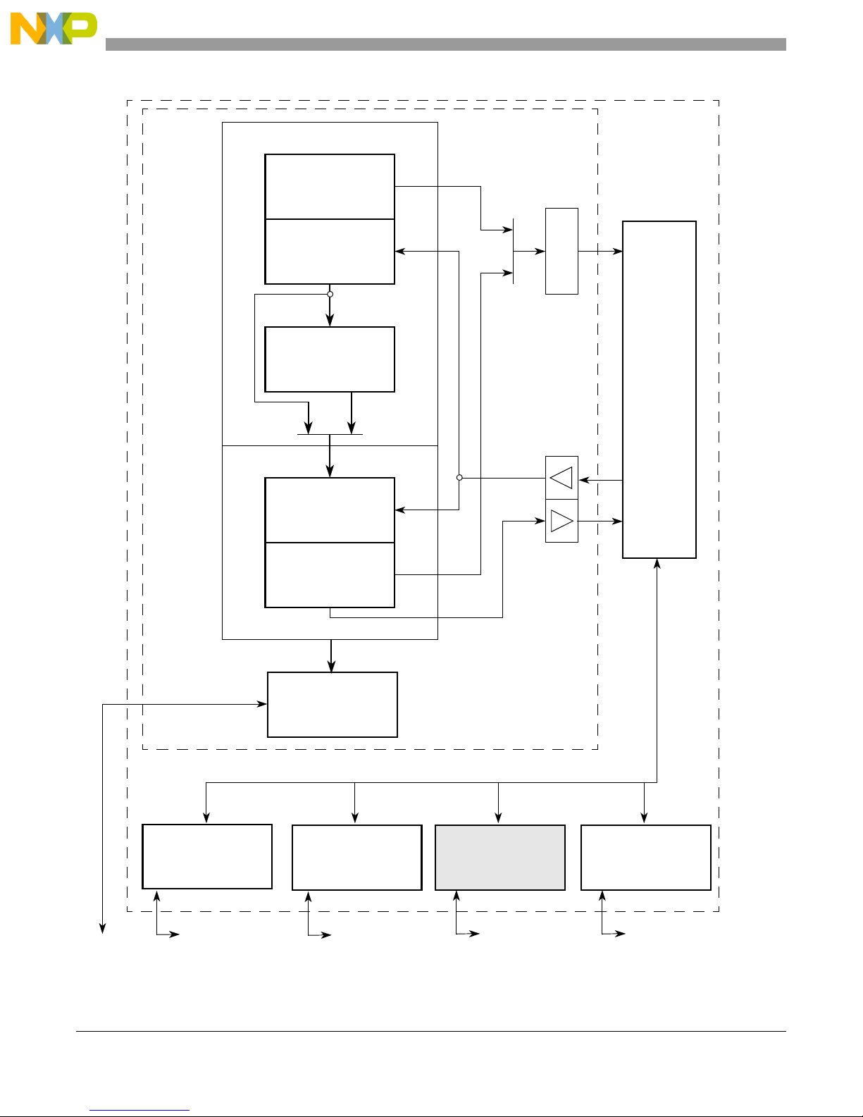
performance ColdFire® V1 core (version 1) family of 32-bit MCUs. Figure 2-1 shows the ColdFire V1
core platform block diagram.
The ColdFire V1 core features are:
• Implements Instruction Set Revision C (ISA_C).
• Supports up to 30 peripheral interrupts and seven software interrupts.
• Built upon lowest-cost ColdFire V2 core microarchitecture.
• Two independent decoupled 2-stage pipelines.
• Debug architecture remapped into S08's single-pin BDM interface.
QE128 Quick Reference User Guide, Rev. 1.0
Freescale Semiconductor 2-1
Page 10
QE MCUs 8-bit and 32-bit Comparison
IA Generation
Instruction
Fetch Cycle
FIFO
Instruction
Buffer
Decode & Select,
Operand Fetch
Address
Generation,
Execute
IFP
OEP
IAG
IC
IB
DSOC
AGEX
BDC/Debug
Flash Array
SRAM Array
Local
Controller
RGPIO
Controller
RGPIO
Pins
BKGD
Bus
Platform
V1 ColdFire
core
On-Platform Bus
Flash
Controller
RAM
Controller
Peripheral
Bridge
Write Data
Read Data
Address,
Attributes
Peripheral Bus
Off-Platform
Off-Platform
Figure 2-1. ColdFire V1 Core Platform Block Diagram
2-2 Freescale Semiconductor
QE128 Quick Reference User Guide, Rev. 1.0
Page 11

QE MCUs 8-bit and 32-bit Comparison
0
Data Registers
3
5D7
31 0
0
Address Register s
3
5A7
310 S
C
CC
The ColdFire V1 core has two programming models, the user and supervisor. First, is the user
programming model which is the same as the M68000 family microprocessors and consists of the
following registers:
• 16 general-purpose 32-bit registers (D0-D7, A0-A7)
• 32-bit program counter (PC)
• 8-bit condition code register (CCR)
D
A
D1
D2
D
D4
D
A1
A2
A
A4
A
P
P
R
Figure 2-2. User Programming Model Registers
Data registers (D0-D7) -- These registers are used for bit, byte, word or longword operations. It can also
be used as index registers for effective address (<ea>) calculations.
313029282726252423222120191817161514131211109876543210
R
W
Figure 2-3. Data Registers (D0–D7)
Data
Address registers (A0-A6) -- These registers can be used as software stack pointers, index registers or
based address registers. They can also be used as data operation
storage,word and longword operations.
313029282726252423222120191817161514131211109876543210
R
W
A7 -- Is a user stack pointer and is treated specifically by CPU.
Program counter (PC) -- This register contains the address of the currently executing instruction. The
PC increments its value or can be loaded with a new one when an instruction
is executing or when an exception occurs.
Freescale Semiconductor 2-3
Address
Figure 2-4. Address Registers (A0–A6)
QE128 Quick Reference User Guide, Rev. 1.0
Page 12

QE MCUs 8-bit and 32-bit Comparison
313029282726252423222120191817161514131211109876543210
R
W
Address
Figure 2-5. Program Counter Register (PC)
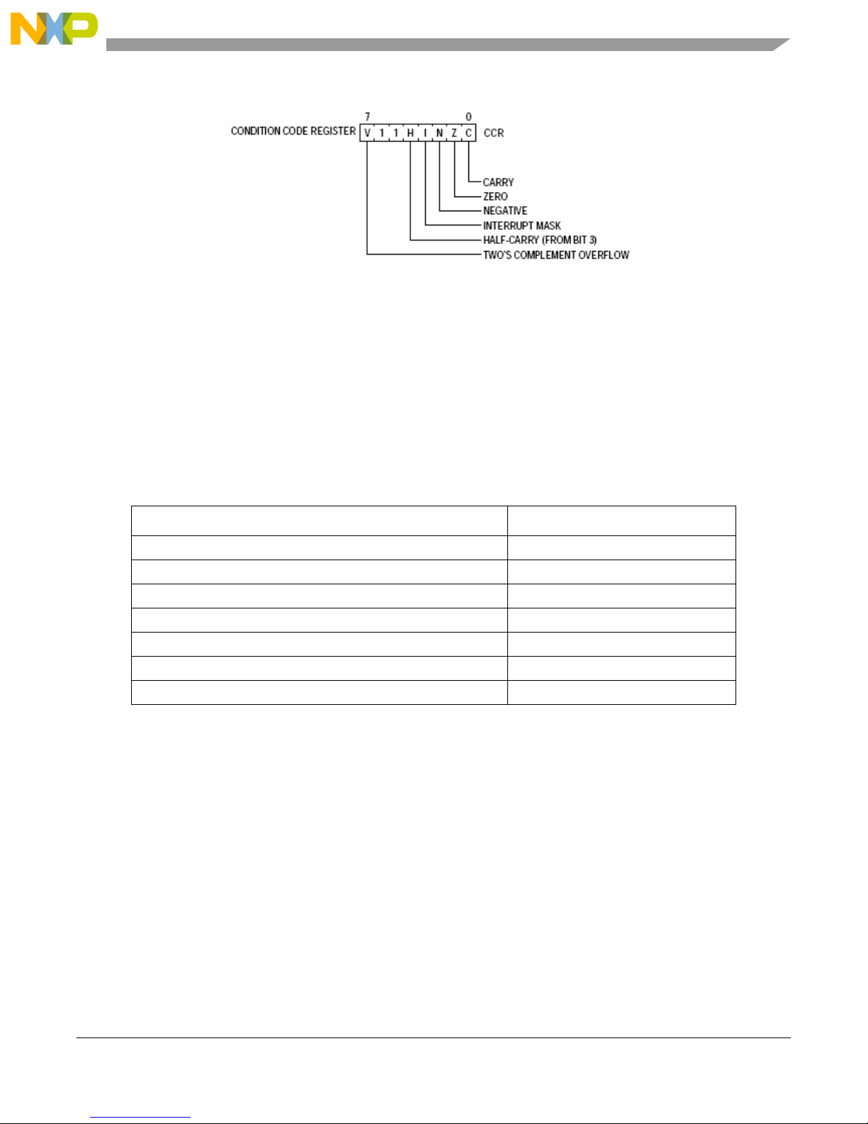
Condition code register (CCR) -- This register reflects the result of most instruction flags. It is used to
evaluate the instructions of the conditional branches.
76543210
R000
W
Figure 2-6. Condition Code Register (CCR)
Table 2-1. CCR Field Descriptions
Field Description
7–5 Reserved, must be cleared.
4
Extend condition code bit. Set to the C-bit value for arithmetic operations; otherwise not affected or set to a specified
X
result.
XNZVC
3
Negative condition code bit. Set if most significant bit of the result is set; otherwise cleared.
N
2
Zero condition code bit. Set if result equals zero; otherwise cleared.
Z
1
Overflow condition code bit. Set if an arithmetic overflow occurs implying the result cannot be represented in operand
V
size; otherwise cleared.
0
Carry condition code bit. Set if a carry out of the operand msb occurs for an addition, or if a borrow occurs in a
C
subtraction; otherwise cleared.
Second, is the supervisor programming model. This is intended to be used only by system control software
to implement restricted operating system functions: I/O control, and memory management. In the
supervisor programming model all registers and features of the ColdFire processors can be accessed and
modified. This consists of registers available in user mode and the following control registers:
• 16-bit status register (SR).
• 32-bit supervisor stack pointer (SSP).
• 32-bit vector base register (VBR).
• 32-bit CPU configuration register (CPUCR).
Status register (SR) — This is a 16-bit register. It stores the processor status and includes the condition
code register (CCR). When it is used in user mode only the lower 8-bit can
be accessed. When used in supervisor mode the registers can be accessed.
If a supervisor instruction is executed in user mode it generates a privilege
violation exception. Figure 2-8 shows the SR behavior in a state machine.
2-4 Freescale Semiconductor
QE128 Quick Reference User Guide, Rev. 1.0
Page 13
System Byte Condition Code Register (CCR)
SR[S] = 1
SR[S] = 0
Reset
Supervisor
Mode
User Mode
Exception
Rte, move-t o- sr with
sr_operand[13] = 1
Rte, move-t o- sr with
sr_operand[13] = 0
1514131211109876543210
000
W
R
0
T
S M
0
I
Figure 2-7. Status Register (SR)
Table 2-2. SR Field Descriptions
Field Description
QE MCUs 8-bit and 32-bit Comparison
X N ZVC
15
Trace enable. When set, the processor performs a trace exception after every instruction.
T
14 Reserved, must be cleared.
13
Supervisor/user state.
S
0User mode
1 Supervisor mode
12
Master/interrupt state. Bit is cleared by an interrupt exception and software can set it during execution of the RTE or
M
move to SR instructions.
11 Reserved, must be cleared.
10–8IInterrupt level mask. Defines current interrupt level. Interrupt requests are inhibited for all priority levels less than or
7–0
CCR
equal to current level, except edge-sensitive level 7 requests, which cannot be masked.
Refer to MCF51QE128 Reference Manual.
Supervisor stack pointer (SSP) -- This ColdFire architecture supports two independent stack pointers,
A7 registers. Each operating mode has its own stack pointer, SSP and user
stack pointer (USP). The hardware implementation of these two registers do
not identify one as SSP and the other as USP . Instead, the hardware uses one
32-bit register as the active A7 and the other as, OTHER_A7.
Freescale Semiconductor 2-5
Figure 2-8. Processor Status State Machine
QE128 Quick Reference User Guide, Rev. 1.0
Page 14

QE MCUs 8-bit and 32-bit Comparison
313029282726252423222120191817161514131211109876543210
R
W
Address
Figure 2-9. Stack Pointer Registers (A7 and OTHER_A7)
Vector base register (VBR) -- This register defines the base addres s of the exception vector table in the
memory. It has two different possible values: 0x(00)00_0000 exception
vector table based on the flash, and 0x(00)80_0000 exception vector table
based on the RAM. At reset the VBR is cleared. The VBR is located at the
base of the exception table at the address 0x(00)00_0000 in the flash.
313029282726252423222120191817161514131211109876543210
R 0 0 0 0 0 000
W
Base
Address
0 0 0 0 0 000000000 000 0 00
Figure 2-10. Vector Base Register (VBR)
CPU configuration register (CPUCR) -- With this register you can configure some cores into supervisor
mode. Certain hardware features can be enabled or disabled based on the
state of the CPUCR.
31 30 29 28 27 26252423222120191817161514131211109876543210
R
ARD IRD IAE IME BWD0FSD
W
0000000 0 0 0 000000000 000 0 00
Figure 2-11. CPU Configuration Register
2.2.1.1 Addressing Modes
The ColdFire V1 core counts with 12 different addressing modes. The addressing modes and syntax are
shown in Table 2-3:
Table 2-3. Addressing Modes and Syntax
Addressing modes Syntax
Register Direct. op.sz
Address Register Indirect. op.sz (Ax),Rx
Address Register Indirect with Post-increment. op.sz (Ax)+,Rx
Address Register Indirect Pre-decrement. op.sz -(Ay),Rx
Address Register Indirect with Displacement. op.sz d16(Ay),Rx
Address Register Indirect with Scaled Index and Displacement. op.sz d8(Ay,Xi*SF),Rx
Program Counter Indirect with Displacement. op.sz d16(PC),Rx
1
Ry,Rx
Program Counter Indirect with Scaled Index and Displacement. op.sz d8(PC,Xi*SF),Rx)
2-6 Freescale Semiconductor
QE128 Quick Reference User Guide, Rev. 1.0
Page 15

QE MCUs 8-bit and 32-bit Comparison
Table 2-3. Addressing Modes and Syntax
Addressing modes Syntax
Absolute Short Addressing. op.sz xxx.w,Rx
Absolute Long Addressing. op.sz xxx.{l},Rx
Immediate Byte, Word. op.{b,w}2 #imm,Rx
3
Immediate Long. op.l#imm
1
op.sz - operand size(size is 1 for byte, 2 for word, 4 for long).
2
op.{b,w} - operand {byte,word}.
3
op.l - operand long.
,Rx
This is a syntax for a V1 core example:
Source Destination
#0x55 Rx
2.2.1.2 Exception Processing
Exception processing is defined as processor-detected conditions that force an instruction stream
discontinuity because of a program or system error: a system call, a debug, or an I/O interrupt. The
ColdFire V1 core uses a reduced version of the interrupt controller from other ColdFire processors. This
hardware implementation is available only for a 32-bit MCU.
Freescale Semiconductor 2-7
QE128 Quick Reference User Guide, Rev. 1.0
Page 16
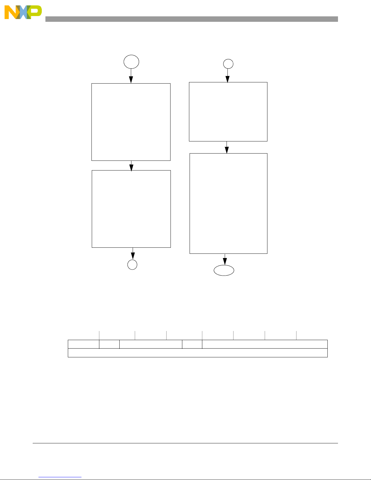
QE MCUs 8-bit and 32-bit Comparison
Saves a copy of the SR.
Forces:
SR[S]=1
SR[T]=0
If an interrupt forces
the interrupt
SR[M]=0
then sets
SR[I]=to the level of
Calculates the vector for
all internal exceptions.
For interrupts, the CPU
uses the vector number
supplied by the interrupt
controller or performs an
interrupt acknowledge
(IACK) cycle to retrieve
the I/O vector number.
Init
Saves the content at the
time of the exception by
storing a 64-bit
exception stack frame
(including the saved SR)
on the top of the
supervisor stack.
The processor fetches a
32-bit vector address
from the exception
vector table @ (VBR +
vector_number x 4). The
address defines the first
instruction of the
exception handler or
interrupts service routine
(ISR). Control is then
passed to the exception
handler at this address.
1
End
1
The processor performs the following operations to process an exception:
Interrupts are treated as lowest-priority exception type. CPU samples for halts and interrupts once per
instruction. The first instruction in ISR does not sample. Interrupts are guaranteed to be recoverable
exceptions.
313029282726252423222120191817161514131211109876543210
Format FS[3:2] Vector FS[1:0] Status Register
Figure 2-12. Processor Operations Process
Figure 2-13. Exception Stack Frame Form
ColdFire architecture reserves 64 entries for processor exceptions and the remaining 192 entries for I/O
interrupts. The ColdFire V1 core architecture only uses a relatively small number of the I/O interrupt
vector. Table 2-4 shows the ColdFire V1 core processor with the exception of the vector table.
QE128 Quick Reference User Guide, Rev. 1.0
Program Counter
2-8 Freescale Semiconductor
Page 17

Table 2 -4. Ve cto r Ta b l e
Vector
Number(s)
Vector
Offset(Hex)
Stacked
Program
Counter
Assignment
0 0x000 - Initial supervisor stack pointer
1 0x004 - Initial program counter
2-63 0x008-0x0FC - Reserved for internal CPU Ex ceptions
64 0x100 Next IRQ_pin
65 0x104 Next Low_voltage
66 0x108 Next TPM1_ch0
67 0x10C Next TPM1_ch1
68 0x110 Next TPM1_ch2
69 0x114 Next TPM1_ovfl
70 0x118 Next TPM2_ch0
71 0x11C Next TPM2_ch1
72 0x120 Next TPM2_ch2
73 0x124 Next TPM2_ovfl
74 0x128 Next SPI2
75 0x12C Next SPI1
76 0x130 Next SCI1_err
77 0x134 Next SCI1_rx
78 0x138 Next SCI1_tx
79 0x13C Next IICx
80 0x140 Next KBIx
81 0x144 Next ADC
82 0x148 Next ACMPx
83 0x14C Next SCI2_err
84 0x150 Next SCI2_rx
85 0x154 Next SCI2_tx
86 0x158 Next RTC
87 0x15C Next TPM3_ch0
88 0x160 Next TPM3_ch1
89 0x164 Next TPM3_ch2
90 0x168 Next TPM3_ch3
91 0x16C Next TPM3_ch4
92 0x170 Next TPM3_ch5
93 0x174 Next TPM3_ovfl
94-95 0x178-0x17C - Reserved; unused for V1
96 0x180 Next Level 7 Software Interrupt
97 0x184 Next Level 6 Software Interrupt
98 0x188 Next Level 5 Software Interrupt
99 0x18C Next Level 4 Software Interrupt
100 0x190 Next Level 3 Software Interrupt
101 0x194 Next Level 2 Software Interrupt
102 0x198 Next Level 1 Software Interrupt
103-255 0x 19C-0x3FC - Reserved; unused for V1
QE MCUs 8-bit and 32-bit Comparison
Freescale Semiconductor 2-9
QE128 Quick Reference User Guide, Rev. 1.0
Page 18
QE MCUs 8-bit and 32-bit Comparison
2.2.2 QE S08 core
This section provides summary information about the registers, addressing modes and core features. The
generated source and object-code is compatible with the M68HC08 CPU.
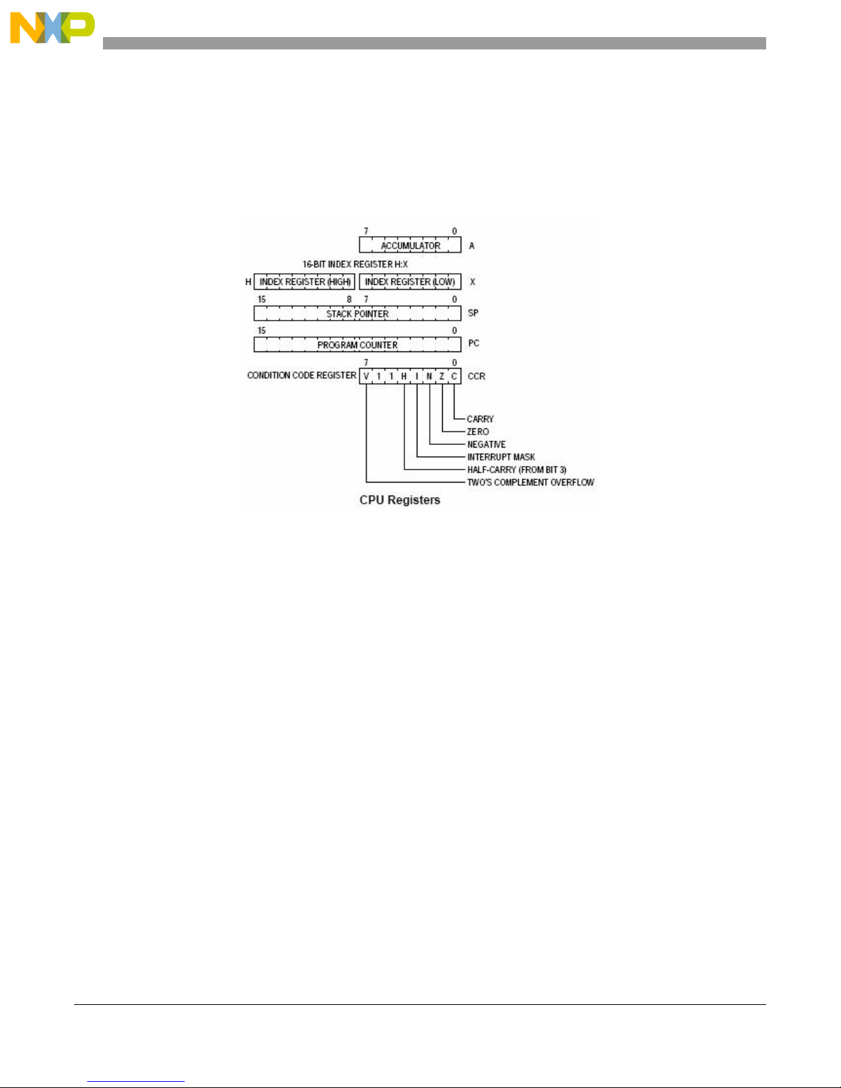
The S08 MCU supports only the user programming model. Figure 2-14 shows five CPU registers. These
registers are not part of the memory map.
Figure 2-14. CPU Registers
Accumulator -- The accumulator is a general-purpose 8-bit register . One operand input to the arithmetic
logic unit (ALU) is connected to the accumulator and the ALU results are
often stored in the accumulator after arithmetic and logical operations.
Index Register (H:X) -- This is a two separate 8-bit register, which often works together as a 16-bit
address pointer where H holds the upper byte of an address and X the lower
byte. All the indexing addressing mode instructions use the 16-bit register.
Stack pointer (SP) -- This 16-bit address pointer register points to the next available location on the
automatic last-in-first-out (LIFO). The stack is used to automatically store
the return address from subroutine calls or return from interrupts. It stores
the context in the interrupt service routine (ISR) and it stores the local
variables and parameters in function calls.
Program counter (PC) -- This register contains the next instruction or operand to be retrieved. This
register automatically increments to the next memory location during a
normal program execution.
Condition code register (CCR) -- This 8-bit condition code register contains the interrupt mask (I) and
five flags that indicate the results of the instruction just executed. Bits 5 and
6 are permanently set to 1.
2-10 Freescale Semiconductor
QE128 Quick Reference User Guide, Rev. 1.0
Page 19
QE MCUs 8-bit and 32-bit Comparison
Figure 2-15. Condition Code Register
V - Two's complement Overflow Flag N - Negative flag
H - Half Carry Flag Z - Zero Flag
I - Interrupt Mask Bit C - Carry/Borrow flag
2.2.2.1 Addressing Modes
Addressing modes define the way the CPU accesses operand and data. The S08 core supports seven
different addressing modes:
Table 2-5. Addressing Modes and Examples
Addressing Modes Example
Inherent --Operands in internal registers. ASLA – Arithmetic Shift Left A.
Relative -- 8-bit offset to branch destination. BEQ rel – Branch if equal
Immediate -- Operand in next object code byte. ADC #opr8i – Add with carry
Direct -- Operand in memory at 0x0000-0x00FF. ADC opr8a – Add with carry
Extended -- Operand within 64 Kbyte address space. ADC opr16a – Add with carry
Indexed relative to H:X. ADC oprx8,X – Add with carry
Indexed relative to SP. ADC oprx8,SP – Add with carry
n -- Any label or expression that evaluates to a single integer in the range 0-7
opr8i -- Any label or expression that evaluates to an 8-bit immediate value
opr16i -- Any label or expression that evaluates to a 16-bit immediate value
opr8a -- Any label or expression that evaluates to an 8-bit value
opr16a -- Any label or expression that evaluates to a 16-bit value
oprx8 -- Any label or expression that evaluates to an unsigned 8-bit value, used for indexed addressing
oprx16 -- Any label or expression that evaluates to a 16-bit value
page -- Any label or expression that evaluates to a valid bank number for PPAGE register. Any value
between 0 and 7 is valid.
rel -- Any label or expression that refers to an address that is within -128 to +127 locations from the next
address after the last byte of object code for the current instruction.
A -- Accumulator
Freescale Semiconductor 2-11
QE128 Quick Reference User Guide, Rev. 1.0
Page 20
QE MCUs 8-bit and 32-bit Comparison
Store PCL in SP
Store X in SP
Store PCH in SP
Store A in SP
Store PCL in SP
Store CCR in SP
Sets the | bit in the CCR
Fetches the high-order
half of the interrupt
vector
Fetches the low-order
half of the interrupt
vector
Delays for one free bus
cycle
Init
1
Fetches three bytes of
program information
starting at the address
indicated by the interrupt
vector
Fills the instruction
queue, preparing for
execution of the first
instruction in the
interrupt service routine
1
2
2
End
2.2.2.2 Interrupt Sequence
The S08 core interrupt sequence first completes the current instruction then attends the requested interrupt.
The CPU responds to an interrupt with the same sequence operation as in a software interrupt (SWI), and
it differs from the address used for the vector retrieved.
Figure 2-16. The CPU Interrupt Sequence
2.2.3 ColdFire V1 or 9S08QE
The ColdFire V1 and S08 cores have significant differences, even though the 32 bit ColdFire V1 core
presents improvements in performance. These differences are highlighted in the following section.
The ColdFire V1 architecture features, staged pipelining allows the core to process multiple instructions
at the same time.
2-12 Freescale Semiconductor
QE128 Quick Reference User Guide, Rev. 1.0
Page 21
QE MCUs 8-bit and 32-bit Comparison
Figure 2-17. V1 Core Pipelines
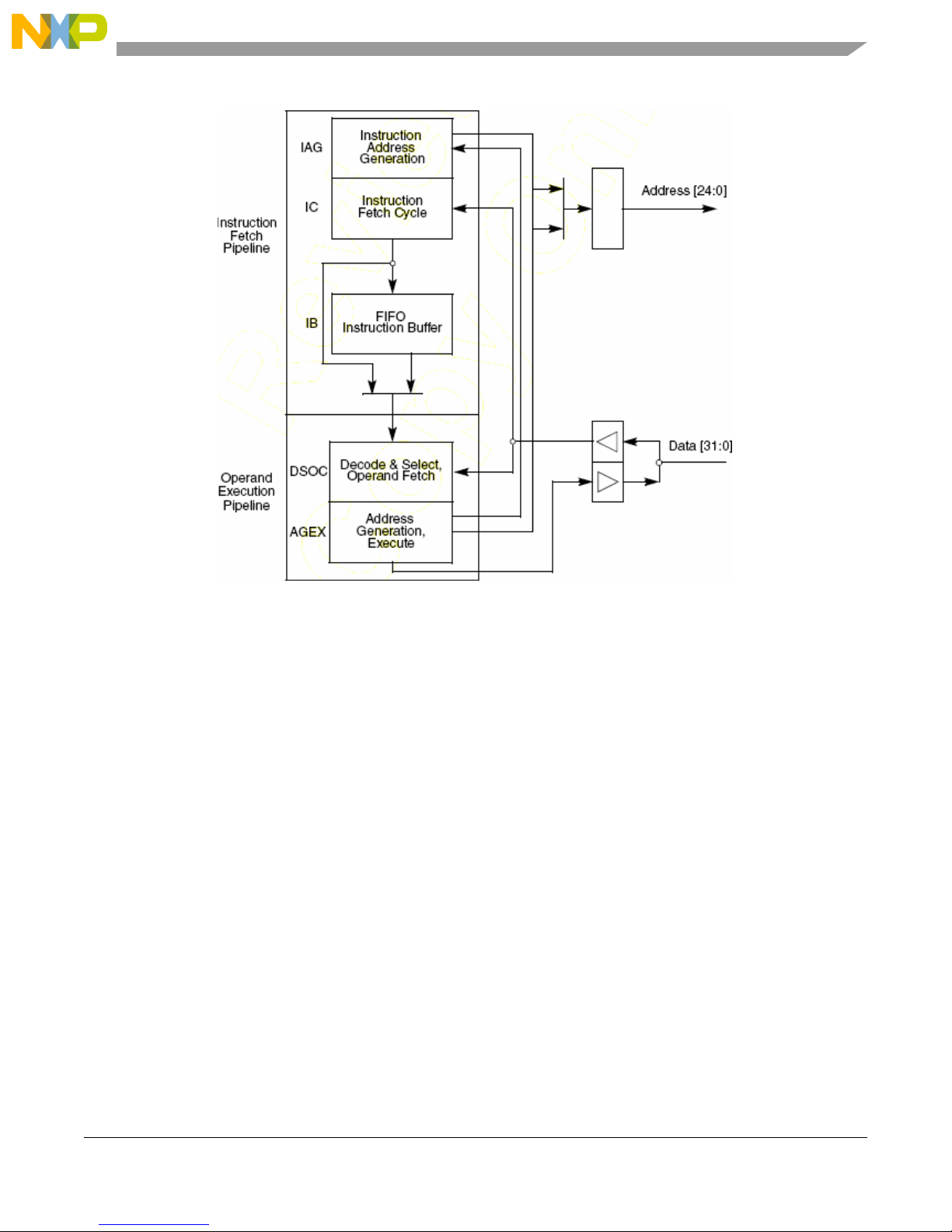
• The V1 Coldfire core pipeline stages include the following:
— Two-stage instruction fetch pipeline (IPF) (plus instruction buffer stage)
— Instruction address generation (IAG) – Calculates the next prefetch address
— Instruction fetch cycle (IC) – Initiates prefetch on the processor’s local bus
— Instruction buffer (IB) – Buffer stage minimizes effects of fetch latency using fifo queue
• Two-stage operand execution pipeline (OEP)
— Decode and select/operand fetch cycle (DSOC) – Decodes instruction and fetches the required
components for effective address calculation, or the operand fetch cycle
— Address generation/execute cycle (AGEX) – Calculates operand address or executes the
instruction
ColdFire V1 core architecture -- Is an orthogonal architecture that has an advantage. It has 16 different
registers for operation that can be used instead of one. The ColdFire V1 core
processes more effectively the 32-bit length operations than the 8-bit core
version.
S08 core architecture -- Is accumulator based, almost all arithmetic and logical instructions use the
accumulator. The S08 can handle 32-bit length operations but requires more
cycles because it executes more instructions, taking more time.
The ColdFire MCU has two programming models with different privileges to control the system. These
programming models are similar to the administrator and user in windows. When the MCU is on the
Freescale Semiconductor 2-13
QE128 Quick Reference User Guide, Rev. 1.0
Page 22

QE MCUs 8-bit and 32-bit Comparison
administrator level it can access all the registers and change values. The 8-bit core version does not count
with this feature.
Table 2-6 shows a global view of the core differences. Detailed information is explained in the beginning
of this chapter. Refer to review Reference Manual MCF51QE128 and MC9S08QE128 at the
www.freescale.com site.
Table 2-6. Comparison of Cores
MC9S08QE128 MCF51QE128
Up to 50 MHz CPU from 3.6 V 2.1 V, and 20 MHz CPU from 2.1 V to 1.8 V across temperature ranged of -40°C
to 85°C.
8-bit HCS08 core. 32-bit ColdFire V1 core.
8-bit data bus, 16-bit address bus. 32-bit data bus, 24-bit address bus.
64 Kb memory map, 16 Kb paging window for
addressing memory beyond 64 Kb. Linear address
pointer for accessing data across entire memory range.
HC08 instruction set with added BGND, CALL and RTC
instructions.
Support for up to 32 interrupt/reset exceptions.
Exception priorities are fixed. One level of interrupt
grouping. No hardware support for nesting.
16 Mb memory map, entire memory map addressed
directly.
ColdFire Instruction Set Revision C (ISA_C), and
additional instructions for efficient handling of 8-bit and
16-bit data.
Support for up to 256 interrupt/reset exceptions (39 are
used on MCF51QE128). Exception priorities are fixed
except for two interrupts that can be remapped. Seven
levels of interrupt grouping and hardware support for
nesting.
Resets: one vector for all reset sources. Vector must
point to address within pages 0-3. No illegal address
reset. Entire memory map is legal.
System reset status (SRS) registers set flags for most recent reset source.
Resets: vectors for up to 64 reset sources. Vector can
point to any valid address. Illegal address reset is
supported.
2.2.3.1 Exception Comparison
Table 2-7 shows the exception differences between 8-bit core and 32-bit core.
Table 2-7. Exception Differences
Attribute S08 V1 ColdFire
Exception Vector Table. 32, 2-byte entries, fixed location at
upper end of memory.
More on Vectors. 2 for CPU + 30 for IRQs (interrupt
requests), reset at upper address.
Exception Stack Frame. 5-byte frame: CCR, A, X, PC. 8-byte frame: F/V, SR, PC;
Interrupt Levels. 1 = f(CCR[I]). 7 = f(SR[I]) with automatic hardware
Non-Maskable IRQ Support. No Yes with level 7 interrupts.
103, 4-byte entries, located at lower end of
memory at reset, relocatable with the VBR.
64 for CPU + 39 for IRQs, reset at lowest
address.
General-purpose registers (An, Dn) must
be saved/restored by the ISR.
support for nesting.
2-14 Freescale Semiconductor
QE128 Quick Reference User Guide, Rev. 1.0
Page 23

QE MCUs 8-bit and 32-bit Comparison
Table 2-7. Exception Differences
Core-enforced IRQ Sensitivity. No Level 7 is edge sensitive, and others level
sensitive.
INTC (interrupt controller)
Vectoring.
Software IACK. No Yes
Exit Instruction from ISR. RTI (real time interrupt). RTE (real time exception).
Fixed priorities and vector
assignments.
Fixed priorities and vector assignments,
plus any 2 IRQs can be remapped as the
highest priority level 6 requests.
2.2.3.2 Code Example Comparison
This example is a code made in C and is compiled and executed for both MCUs,V1 and S08. Both results
present a difference in execution time. The generated assembly lines are similar.
There are two four loop cycles that nest within this endless loop.The inner loop cycle counts from 0 to 100
and stores the k variable value in the buffer k array. The outer loop counts from 0 to 60000. The i variable
counter increments every time the k variable counter reaches the 101 value.
void main(void) {
unsigned int i,k;
unsigned int buffer[100];
SOPT1 = 0x23; // Watchdog disable. Stop Mode Enable. Background Pin
// enable. RESET pin enable
for(;;) {
for (i=0; i<=60000; i++) { // This rutine is executed 60001
for (k=0; k<=100; k++) {
buffer[k] = k;
}
}
} // loop forever
// please make sure that you never leave main
}
Assembly code lines generated for the S08 MCU; observe the difference between this assembly code and
the assembly code generated from the ColdFire V1 core.
10: SOPT1 = 0x23; // Watchdog disable. Stop Mode Enable. Background Pin enable. RESET pin
enable
0004 a623 [2] LDA #35
0006 c70000 [4] STA _SOPT1
0009 L9:
11: for(;;) {
12:
13: for (i=0; i<=60000; i++) {
0009 95 [2] TSX
000a 6f03 [5] CLR 3,X
000c 6f02 [5] CLR 2,X
000e LE:
14: for (k=0; k<=100; k++) {
000e 95 [2] TSX
000f 6f01 [5] CLR 1,X
Freescale Semiconductor 2-15
QE128 Quick Reference User Guide, Rev. 1.0
Page 24

QE MCUs 8-bit and 32-bit Comparison
0011 7f [4] CLR ,X
0012 L12:
15: buffer[k] = k;
0012 95 [2] TSX
0013 e601 [3] LDA 1,X
0015 48 [1] LSLA
0016 af04 [2] AIX #4
0018 87 [2] PSHA
0019 9f [1] TXA
001a 8b [2] PSHH
001b 95 [2] TSX
001c eb01 [3] ADD 1,X
001e e701 [3] STA 1,X
0020 86 [3] PULA
0021 a900 [2] ADC #0
0023 87 [2] PSHA
0024 e602 [3] LDA 2,X
0026 8a [3] PULH
0027 88 [3] PULX
0028 f7 [2] STA ,X
0029 9ee602 [4] LDA 2,SP
002c e701 [3] STA 1,X
002e 95 [2] TSX
002f 6c01 [5] INC 1,X
0031 2601 [3] BNE L34 ;abs = 0034
0033 7c [4] INC ,X
0034 L34:
0034 9efe01 [5] LDHX 1,SP
0037 650064 [3] CPHX #100
003a 23d6 [3] BLS L12 ;abs = 0012
003c 95 [2] TSX
003d 6c03 [5] INC 3,X
003f 2602 [3] BNE L43 ;abs = 0043
0041 6c02 [5] INC 2,X
0043 L43:
0043 9efe03 [5] LDHX 3,SP
0046 65ea60 [3] CPHX #-5536
0049 23c3 [3] BLS LE ;abs = 000e
16: }
17: }
18:
19: PTED = 0xFF;
004b 6eff00 [4] MOV #-1,_PTED
004e 20b9 [3] BRA L9 ;abs = 0009
20: } // loop forever
21: // please make sure that you never leave main
22: }
23:
Assembly lines generated for the MCF51QE128 MCU.
; 10: SOPT1 = 0x23; // Watchdog disable. Stop Mode Enable. Background Pin enable.
RESET pin enable
; 11: for(;;) {
; 12:
;
0x00000004 0x7023 moveq #35,d0
0x00000006 0x11C09802 move.b d0,0xffff9802
2-16 Freescale Semiconductor
QE128 Quick Reference User Guide, Rev. 1.0
Page 25

QE MCUs 8-bit and 32-bit Comparison
;
; 13: for (i=0; i<=60000; i++) {
;
0x0000000A 0x4280 clr.l d0
0x0000000C 0x6016 bra.s *+24 ; 0x00000024
;
; 14: for (k=0; k<=100; k++) {
;
0x0000000E 0x4281 clr.l d1
0x00000010 0x6008 bra.s *+10 ; 0x0000001a
;
; 15: buffer[k] = k;
;
0x00000012 0x41D7 lea (a7),a0
0x00000014 0x21811C00 move.l d1,(a0,d1.l*4)
;
; 16: }
;
0x00000018 0x5281 addq.l #1,d1
0x0000001A 0x0C8100000064 cmpi.l #100,d1 ; '...d'
0x00000020 0x63F0 bls.s *-14 ; 0x00000012
;
; 17: }
; 18:
;
0x00000022 0x5280 addq.l #1,d0
0x00000024 0x0C800000EA60 cmpi.l #60000,d0 ; '...`'
0x0000002A 0x63E2 bls.s *-28 ; 0x0000000e
;
; 19: PTED = 0xFF;
;
0x0000002C 0x103C00FF move.b #-1,d0 ; '.'
0x00000030 0x11C08008 move.b d0,0xffff8008
;
; 20: } /* loop forever */
;
0x00000034 0x60D4 bra.s *-42 ; 0x0000000a
0x00000036 0x51FC trapf
Table 2-8 shows the CPU cycles needed and the assembly lines code generated to complete the execution
of the program described above. The used compiler for this test was CW 6.0 version and no optimization
tool was used.
This example is just a particular comparison and the performance between
cores is not reflected with this example. The performance is application
dependant.
Table 2-8. Comparison of CPU Cycles and Assembly Code Lines
Assembly lines code 18 43
CPU Cycles 49,201,507 407,947,991
Freescale Semiconductor 2-17
NOTE
MCF51QE128 MC9S08QE128
QE128 Quick Reference User Guide, Rev. 1.0
Page 26

QE MCUs 8-bit and 32-bit Comparison
2.3 Features Comparison
2.3.1 On-Chip Memory Comparison
Table 2-9. On-Chip Memory Comparison
MC9S08QE128 MCF51QE128
Peripheral register maps maintain relative addresses.
Up to 8 Kb of random-access memory (RAM).
FLASH read/program/erase over full operating voltage and temperature.
Up to 128KB of FLASH, two FLASH arrays of 64Kb x
8-bits arranged in series. Two flash arrays allow for
“read while write” programming.
Security circuitry to prevent unauthorized access to
RAM and FLASH contents, default is secured when
blank
2.3.2 Power-Saving Modes and Power-Saving Features Comparison
Table 2-10. Power-Saving mode Comparison
Up to 128 KB of FLASH. Two FLASH arrays of 64 Kb x
8-bits arranged in parallel. FLASH “read while write” not
supported.
Security circuitry to prevent unauthorized access to
RAM and FLASH contents, default is unsecured when
blank
MC9S08QE128 MCF51QE128
Two very low power stop modes (Stop2 and Stop3).
Low Power run (LPRun) and wait (LPWait) modes allow for use of peripherals in reduced-current and
reduced-speed mode.
Peripheral clock enable register can disable clocks to unused modules, thereby reducing currents.
Very low power external oscillator that can be used in stop modes to provide accurate clock source RTC module.
Very low power real time counter for use in run, wait, and stop modes with internal and external clock sources.
6µs typical wake up time from stop modes.
Reduced power wait mode (enabled by WAIT
instruction).
2.3.3 Package Comparison
Table 2-11. Package Comparison
MC9S08QE128 MCF51QE128
Pin-to-pin compatible in 80-LQFP and 64-LQFP packages.
Additional 48-QFN, 44-QFP and 32-LQFP packages. No additional packages.
Reduced power wait mode (enabled by setting WAIT bit
in the SOPT1 register then executing STOP
instruction).
2-18 Freescale Semiconductor
QE128 Quick Reference User Guide, Rev. 1.0
Page 27

2.3.4 Clock Comparison
Table 2-12. Clock Comparison
MC9S08QE128 MCF51QE128
Oscillator (XOSC) – Loop-control pierce oscillator, crystal or ceramic resonator range of 31.25 kHz to 38.4 kHz
or 1 MHz to 16 MHz
Internal clock source (ICS) – Internal clock source module containing a frequency-locked-loop (FLL) controlled
by internal or external reference. Precision trimming of internal reference allows 0.2% resolution and 2%
deviation over temperature and voltage. Supports CPU frequencies from 2 MHz to 50 MHz
2.3.5 System Comparison
Table 2-13. System Comparison
MC9S08QE128 MCF51QE128
Watchdog computer operating properly (COP) reset with option to run from dedicated 1 kHz internal clock source
or bus clock.
Low-voltage detection with reset or interrupt. Selectable trip points.
Illegal opcode detection with reset.
No illegal address reset, all addresses in maps are
legal.
QE MCUs 8-bit and 32-bit Comparison
Illegal address detection with reset.
FLASH Block protection: protects in 1k increments.
Protects array 0 first (from 0x0FFFF - 0x00000), then
array 1 (from 0x1FFFF – 0x10000).
2.3.6 Input/Output Comparison
Table 2-14. Input/Output Comparison
MC9S08QE128 MCF51QE128
70 GPIOs (general purpose input/output) and 1 input-only and 1 output-only pin.
16 KBI (keyboard interrupts) with selectable polarity.
Hysteresis and configurable pull up device on all input pins, configurable slew rate and drive strength on all output
pins.
SET/CLR registers on 16 pins (PTC and PTE).
Rapid I/O not featured. Selectable Rapid I/O supported on PTC and PTE ports.
FLASH Block protection: protects in 2 k increments.
Protects array from 0x00000 to 0x1FFFF.
Freescale Semiconductor 2-19
QE128 Quick Reference User Guide, Rev. 1.0
Page 28

QE MCUs 8-bit and 32-bit Comparison
2.3.7 Development Support Comparison
Table 2-15. Development Support Comparison
MC9S08QE128 MCF51QE128
Single-wire background debug interface. Same hardware Background Debug Mode (BDM) cable supports both
devices.
One version of CodeWarrior integrated development environment (IDE) and debugger supports both devices.
CodeWarrior stationary, project wizard, initialization wizard and Processor Expert make C-code migration
between devices easy.
SET/CLR registers on 16 pins (PTC and PTE).
Break point capability to allow single breakpoint setting
during in-circuit debugging, plus three more
breakpoints in on-chip debug module.
Integrated ColdFire DEBUG_Rev_B+ interface with
single wire BDM connection supports the same
electrical interface used by the S08 family debug
modules.
On-chip in-circuit emulator (ICE) debug module
containing three comparators and nine trigger modes.
Eight deep FIFO for tracing change-of-flow addresses
and event-only data. Debug module supports both tag
and force breakpoints.
2.3.8 Peripherals Comparison
Table 2-16. Peripherals Comparison
MC9S08QE128 MCF51QE128
ADC – 24-Channel, 12-bit resolution, 2.5 µs conversion time, automatic compare function, 1.7 mV/°C
temperature sensor, internal bandgap reference channel, operation in stop3, and fully functional from 3.6 V to
1.8 V.
ACMPx – Two analog comparators with selectable interrupt on rising, falling, or either edge of comparator output,
compare option to fixed internal bandgap reference voltage, and operation in stop3.
SCIx – Two serial communications interface modules with optional 13-bit break.
SPIx – Two serial peripheral interfaces with Full-duplex or single-wire bidirectional, double-buffered transmit and
receive, Master or Slave mode, MSB-first or LSB-first shifting.
IICx – Two IICs with up to 100 kbps with maximum bus loading, multi-master operation, programmable slave
address, Interrupt driven byte-by-byte data transfer, supports broadcast mode and 10-bit addressing.
Classic ColdFire Debug B+ functionality mapped into
the single-pin BDM interface. 64 deep FIFO for tracing
processor status (PST) and debug data (DDATA). Real
time debug support, with 6 hardware breakpoints, four
PC, one address and one data, that can be configured
into a 1 or 2 level trigger with a programmable response.
TPMx – One 6-channel (TPM3) and two 3-channel (TPM1 and TPM2), selectable input capture, output compare,
or buffered edge- aligned or center-aligned PWM on each channel, and operation in stop3.
RTC – (Real time counter) 8-bit modules counter with binary or decimal based prescaler; external clock source
for precise time base, time-of-day, calendar or task scheduling functions; Free running on-chip low power
oscillator (1 kHz) for periodical wake-up without external components; runs in all MCU modes
2-20 Freescale Semiconductor
QE128 Quick Reference User Guide, Rev. 1.0
Page 29

Chapter 3
How to Load the QRUG Examples?
3.1 Overview
This section describes the steps needed to download the firmware to flash. This shows the modules
working in the hardware.
All the examples described in this document are developed using Code Warrior 6.0 version and can be
changed in order to fit the application. T o run these examples a Code W arrior version 6.0 and an Evaluation
Board or a Demo board are needed in order to run these examples satisfactorily.
3.2 Steps to programming the MCU using Multilink
Follow these simple steps in order to load the QRUG examples and download it to the device. The
explanation works for the EVB and Demo board.
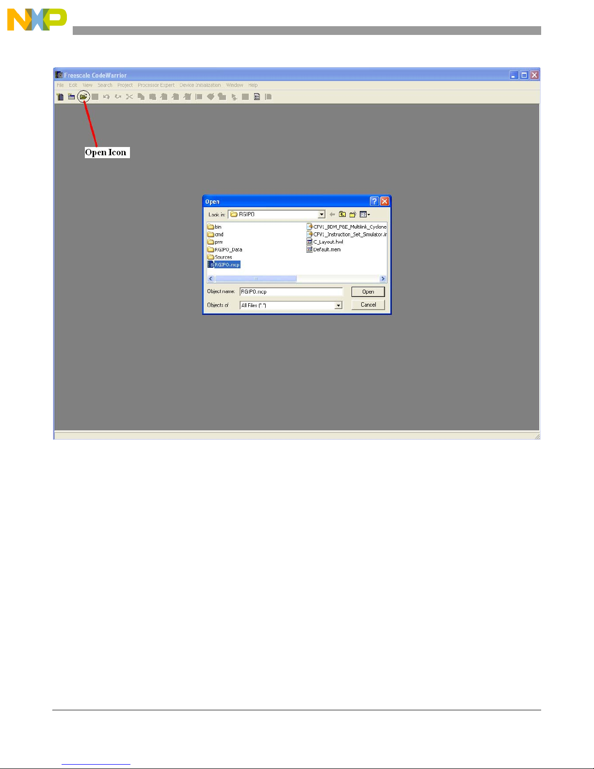
1. Open CodeWarrior 6.0.
2. File -> Open, or click on the Open Icon as shown in Figure 3-1.
Freescale Semiconductor 3-1
QE128 Quick Reference User Guide, Rev. 1.0
Page 30
How to Load the QRUG Examples?
Figure 3-1. Open the Desired Project
3. Browse the desired project.
4. Double click on the .mcp extension file, in this case RGPIO.mcp.
5. To open the file double click on .c extension file (main.c).
6. On the left side of the window is a combo box. Select the P&E Multilink/Cyclone Pro option as
shown in Figure 3-2. The BDM multilink hardware for programming the MCU is needed when an
EVB is used. This device is developed by PEmicro. If a demo board is used do not buy a multilink.
QE128 Quick Reference User Guide, Rev. 1.0
3-2 Freescale Semiconductor
Page 31

How to Load the QRUG Examples?
Figure 3-2. Select the Correct Option in the Combo Box
7. There are three different ways to compile the project. Click on the make icon, beside the combo
box, as shown in Figure 3-3. The make command can be accessed from the Project menu, -> Make,
or just press F7 key on your keyboard.
8. No errors should show up.
9. Project –> Debug. Click on the debug icon beside the make icon, or just press F5 on the keyboard.
Doing this launches the debugger and downloads the program to the MCU flash.
QE128 Quick Reference User Guide, Rev. 1.0
Freescale Semiconductor 3-3
Page 32

How to Load the QRUG Examples?
Make Icon
Debug Icon
Figure 3-3. Make Icon and Debug Icon
10. After the debug command is executed a window pops up (see Figure 3-4). Click on the Connect
option.
QE128 Quick Reference User Guide, Rev. 1.0
3-4 Freescale Semiconductor
Page 33
How to Load the QRUG Examples?
Figure 3-4. Connect Option
11. If a window appears asking to erase and program flash, click Yes.
12. The True-time simulator window appears on your screen. In this window debug the projects,
review the registers and memory in real time.
13. Click on the run button as shown in Figure 3-5. This figure shows the true-time simulator window
or debugger window. This makes the MCU start to execute the project.
QE128 Quick Reference User Guide, Rev. 1.0
Freescale Semiconductor 3-5
Page 34

How to Load the QRUG Examples?
Start/Continue Button
Figure 3-5. Run/Continue Icon
3.3 Steps to programming the MCU Using In-Circuit BDM
Follow these simple steps in order to load the QRUG examples and download it to the device. The
explanation works for EVB only.
1. Open CodeWarrior 6.0.
2. File -> Open, or click on the Open Icon as shown in Figure 3-6.
QE128 Quick Reference User Guide, Rev. 1.0
3-6 Freescale Semiconductor
Page 35

How to Load the QRUG Examples?
Figure 3-6. Open the Desired Project
3. Browse the desired project.
4. Double click on the .mcp extension file, in this case RGPIO.mcp.
5. To open the file, double click on .c extension file (main.c).
6. On the left side of the window is a combo box. Select the SofTec option as shown in Figure 3-7.
QE128 Quick Reference User Guide, Rev. 1.0
Freescale Semiconductor 3-7
Page 36

How to Load the QRUG Examples?
Figure 3-7. Select the Correct Option in the Combo Box
7. There are three different ways to compile the project.
8. Click on the make icon, beside the combo box, as shown in Figure 3-8. The make command can
be accessed from the Project menu, -> Make, or just press F7 key on your keyboard.
9. No errors show up.
10. Project –> Debug. Also click on the debug icon beside the make icon, or just press F5 on the
keyboard. Doing this launches the debugger and downloads the program to the MCU flash.
QE128 Quick Reference User Guide, Rev. 1.0
3-8 Freescale Semiconductor
Page 37
How to Load the QRUG Examples?
Make Icon
Debug Icon
Figure 3-8. Make Icon and Debug Icon
11. After the debug command is executed a window pops up (see Figure 3-9), select the EVBQE128
hardware model and then click on the Connect option.
QE128 Quick Reference User Guide, Rev. 1.0
Freescale Semiconductor 3-9
Page 38

How to Load the QRUG Examples?
F
Figure 3-9. Connect Option
12. A new window may appear asking to erase and program flash, click Yes.
13. The True-time simulator window appears on the screen. In this window debug the projects, review
the registers and memory in real time.
14. Click on the run button as shown in Figure 3-10. This figure shows the true-time simulator window
or debugger window. This makes the MCU start to execute the project.
QE128 Quick Reference User Guide, Rev. 1.0
3-10 Freescale Semiconductor
Page 39

How to Load the QRUG Examples?
Start/Continue button
Figure 3-10. Run/Continue Icon
QE128 Quick Reference User Guide, Rev. 1.0
Freescale Semiconductor 3-11
Page 40

How to Load the QRUG Examples?
3-12 Freescale Semiconductor
QE128 Quick Reference User Guide, Rev. 1.0
Page 41

Chapter 4
KBIxSC KBF KBACK KBIE KBMOD
Module Configuration
KBF – set when event occurs
KBACK – clears KBF
KBI Quick Reference
KBIxPE KBIPE7 KBIPE6 KBIPE5 KBIPE4 KBIPE3 KBIPE2 KBIPE1 KBIPE0
KBI Pin Enable
KBIPE[7:0] — enables and disables each port pin to operate as a keyboard interrupt pin.
KBIxES KBEDG7 KBEDG6 KBEDG5 KBEDG4 KBEDG3 KBEDG2 KBEDG1 KBEDG0
KBI Pin Enable
KBEDG[7:0] – determines the polarity edge that is recognized as a trigger event for the
KBIE – interrupt enable
KBMOD – mode select
corresponding pin.
Because there is more than one KBI module on this device, there may be more than one full
set of registers on your device. In the register name below, where there's a small x, there
would be a 1 or a 2 in your software to distinguish the register that is on KBI1 from KBI2 .
Using the Keyboard Interrupt (KBI) for the QE
Microcontrollers
4.1 Overview
This is a quick reference for using the keyboard interrupt (KBI) module for the QE family
microcontrollers (MCUs). Basic information about the functional description and configuration options
are provided.
The following example may be modified to suit an application. The KBI project is made for the
MC9S08QE128 and MCF51QE128 MCUs.
4.2 KBI project for EVB
4.2.1 Code example and explanation
This example code is available from the Freescale Web site www.freescale.com
Freescale Semiconductor 4-1
QE128 Quick Reference User Guide, Rev. 1.0
Page 42

Using the Keyboard Interrupt (KBI) for the QE Microcontrollers
In this application, four of the KBI pins are used to trigger an interrupt routine that toggles an LED every
time a keyboard event is detected. The MCU is programmed to:
• Have four KBI pins (PTD4, PTD5, PTD6 and PTD7), as the interrupt trigger.
• Detect falling edges only on the selected pins
• Generate a hardware interrupt where the LED toggle routine is serviced.
The functions for KBI.mcp project are:
• main – Endless loop waiting for a KBI interrupt.
• MCU_Init – MCU initialization, watchdog disable and the KBI clock module enabled.
• GPIO_Init – Configure PTE0 pin as output.
• KBI_Init – KBI module configuration.
• KBI_ISR – routine that toggles an LED every time an interrupt is generated.
The code below executes the instructions to disable the watchdog, enable the Reset option and background
pin. The System Option Register 1 (SOPT1) is used to configure the MCU. The SCGC1 and SCGC2 are
registers used for power saving consumption, here the bus clock to peripherals can be enabled or disabled.
In this example only the bus clock to the KBI module is active. The clocks to the other peripherals are
disabled.
void MCU_Init(void) {
SOPT1 = 0x23; // Watchdog disable. Stop Mode Enable. Background Pin
// enable. RESET pin enable
SCGC1 = 0x00; // Disable Bus clock to unused peripherals
SCGC2 = 0x10; // Bus Clock to the KBI module is enabled
}
This is the General Purpose Input/Output configuration. These code lines configure the direction for the
PTE port. Eight LEDs from the EVB are connected to the PTE port. The PTE0 is configured as output in
order to drive a LED.
void GPIO_Init(void) {
PTEDD = 0x01; // Configure PTE0 pin as output
PTED = 0x00; // Put 0's in PTE port
}
This is the initialization code for the keyboard interrupt using the QE128 MCU. For this example, both
KBI registers (KBIxSC and KBIxPE) are used to configure the module to detect only falling edges and
enable P T D4 to PTD7 as KBI. During the initialization phase the interrupts are masked. It takes time for
the internal pull up to reach a ‘1’ logic value. After the false interrupts are cleared, the keyboard interrupt
is unmasked.
void KBI_Init(void) {
KBI2SC = 0x06; // KBI interrupt request enabled. Detects edges only
KBI2PE = 0xF0; // PTD4, PTD5, PTD6 and PTD7 enabled as Keyboard interrupts
KBI2ES = 0x00; // Pins detects falling edge
}
This is the main function, above are the described called functions, and all the interrupts are enabled. After
this the keyboard interrupt can be serviced.
void main(void) {
MCU_Init(); // Function that initializes the MCU
4-2 Freescale Semiconductor
QE128 Quick Reference User Guide, Rev. 1.0
Page 43

Using the Keyboard Interrupt (KBI) for the QE Microcontrollers
GPIO_Init(); // Function that initializes the Ports of the MCU
KBI_Init(); // Function that initializes the KBI module
EnableInterrupts; // enable interrupts
for(;;) {
} // loop forever
// please make sure that you never leave this function
}
NOTE
This is the KBI service routine. Every time an interrupt is detected this
routine toggles a LED. The VectorNumber_Vkeyboard can be replaced by
the interrupt vector number. This depends, if the MCU is a 9S08 or V1.
Using this example makes the code fully compatible for either MCU.
void interrupt VectorNumber_keyboard KBI_ISR(void) {
// KBI interrupt vector number = 18 (S08)
// KBI interrupt vector number = 80 (V1)
KBI2SC_KBACK = 1; // Clear the KBI interrupt flag
PTED_PTED0 ^= 1; // Toggles PTE0
}
4.2.2 Hardware Implementation
This project is developed using the EVBQE128 STARTER KIT and can be downloaded at
www.freescale.com. No extra hardware is needed.
Freescale Semiconductor 4-3
QE128 Quick Reference User Guide, Rev. 1.0
Page 44
Using the Keyboard Interrupt (KBI) for the QE Microcontrollers
If the use of other KBI pins are required, extra hardware is easy to install. A push button, a resistor and a
capacitor are used to build the circuit. Figure 4-1 shows the hardware configuration.
Figure 4-1. EVB KBI Hardware Implementation
This example is developed using the CodeWarrior IDE version 6.0 for the
HCS08 and V1 families. It is expressly made for the MCF51QE128 and
MC9S08QE128 (80-pin package). There may be changes needed in the
code to initialize another MCU.
4-4 Freescale Semiconductor
NOTE
QE128 Quick Reference User Guide, Rev. 1.0
Page 45

Using the Keyboard Interrupt (KBI) for the QE Microcontrollers
Figure 4-1, shows hardware connections used for the KBI project. For
detailed information about the MCU supply voltages needed, please refer to
the Pins and Connections chapter in the Reference Manual (MC9S08QE128
or MCF51QE128). It can also be found at www.freescale.com.
4.3 KBI project for Demo board
4.3.1 Code example and explanation
This example code is available from the Freescale Web site www.freescale.com.
This section explains the differences of the codes used in EVB and the Demo board. The codes are the
same.
The functions for KBI.mcp project are:
• main – Endless loop waiting for a KBI interrupt.
• MCU_Init – MCU initialization, watchdog disable and the KBI clock module enabled.
• GPIO_Init – Enables internal pull-ups. Configures PTC0 pin as output.
• KBI_Init – KBI module configuration.
• KBI_ISR – routine that toggles a LED every time an interrupt is generated.
This is the General Purpose Input/Output configuration These code lines configure the direction for the
PTC port. Only six LEDs from the demo board are connected to the PTC port. The other two LEDs are
connected to the E port. In this example only PTC0 is configured as output in order to drive a LED. The
demo board does not count with any pull-ups; therefore the internal pull-up is enabled for the PTA2 and
PTA3 pins.
void GPIO_Init(void) {
PTAPE = 0x0C; // Enable PTA2 and PTA3 pins Internal Pullups
PTCDD = 0x01; // Configure PTC0 pin as output
PTCD = 0x01; // Put 0's in PTC0 pin
}
This is the initialization code for the keyboard interrupt using the QE128 MCU. For this example, both
KBI registers (KBIxSC and KBIxPE) are used to configure the module to detect only falling edges and
enable P TA2 and PTA3 as KBI. During the initialization phase, the interrupts are masked. It takes time for
the internal pull up to reach a ‘1’ logic value. After the false interrupts are cleared, the keyboard interrupt
is unmasked.
void KBI_Init(void) {
KBI1SC = 0x06; // KBI interrupt request enabled. Detects edges only
KBI1PE = 0x0C; // PTA2 and PTA3 enabled as Keyboard interrupts
KBI1ES = 0x00; // Pins detects falling edge
}
Freescale Semiconductor 4-5
QE128 Quick Reference User Guide, Rev. 1.0
Page 46

Using the Keyboard Interrupt (KBI) for the QE Microcontrollers
NOTE
This is the keyboard interrupt service routine. Every time an interrupt is
detected this routine toggles a LED. The VectorNumber_Vkeyboard can be
replaced by the interrupt vector number, this depends if the MCU is a 9S08
or V1. Using this example makes the code fully compatible for either MCU.
void interrupt VectorNumber_Vkeyboard KBI_ISR(void) {
KBI1SC_KBACK = 1; // Clear the KBI interrupt flag
PTCD_PTCD0 ^= 1; // Toggles PTC0
}
4.3.2 Hardware Implementation
This project was developed using the DEMOQE board. No extra hardware is needed.
4-6 Freescale Semiconductor
QE128 Quick Reference User Guide, Rev. 1.0
Page 47
Using the Keyboard Interrupt (KBI) for the QE Microcontrollers
Figure 4-2. Demo Board KBI Hardware Implementation.
This example is developed using the CodeWarrior IDE version 6.0 for the
HCS08 and V1 families. It is expressly made for the MCF51QE128 and
MC9S08QE128 (64-pin package). There may be changes needed in the
code to initialize another MCU.
Figure 4-2, shows the hardware connections used for the KBI project, for
detailed information about the MCU supply voltages needed, please refer to
the Pins and Connections chapter in the Reference Manual (MC9S08QE128
or MCF51QE128). It can also be found at www.freescale.com.
Freescale Semiconductor 4-7
NOTE
QE128 Quick Reference User Guide, Rev. 1.0
Page 48

Using the Keyboard Interrupt (KBI) for the QE Microcontrollers
4-8 Freescale Semiconductor
QE128 Quick Reference User Guide, Rev. 1.0
Page 49

Chapter 5
Using the Internal Clock Source (ICS) for the QE
Microcontrollers
5.1 Overview
This is a quick reference for using the internal source clock (ICS) module for the QE family
microcontrollers (MCUs). Basic information about the functional description and configuration options
are provided. The following example may be modified to suit an application. The ICS project is made for
the MC9S08QE128 and MCF51QE128 MCUs.
ICS Quick Reference
ICS1 CLKS RDIV IREFS IRCLKEN IREFSTEN
Module Configuration:
CLKS - Clock Source Select IRCLKEN - Internal Reference Clock Enable
RDIV - Reference Divider IREFSTEN - Internal Reference Stop Enable
IREFS - Internal Reference Select
ICS2 BDIV RANGE HGO LP EREFS ERCLKEN EREFSTEN
Module Configuration:
BDIV - Bus Frequency Divider EREFS - External Reference Select
RANGE - Frequency Range Select ERCLKEN - External Reference Enable
HGO - High Gain Oscillator Select EREFSTEN - External Reference Stop Enable
LP - Low Power Select
ICSRM TRIM
Internal oscillator trim value: higher value = slower frequency
ICSSC DRST/DRS DMX32 IREFST CLKST OSCINIT FTRIM
Module Status:
DRST - DCO Range Status / DRS - DCO Range Select CLKST - Clock Mode Status
DMX32 - DCO Maximum frequency with 32.768 kHz reference OSCINIT - OSC Initialization
IREFST - Internal Reference Status FTRIM - ICS Fine Trim
5.2 Code Example and Explanation
The project ICS.mcp shows how to configure the ICS module for the QE family MCUs. The main
functions are:
• main — Endless loop toggling a LED.
• MCU_Init – MCU initialization, watchdog disable.
• GPIO_Init – Configure PTE0 pin as output.
QE128 Quick Reference User Guide, Rev. 1.0
Freescale Semiconductor 5-1
Page 50

Using the Internal Clock Source (ICS) for the QE Microcontrollers
• ICS_Init – ICS module configuration
This example configures one of six modes of operation for the ICS module.
These are the four definitions used in the ICS code source. You need to uncomment the desired mode and
compile the project. This makes the MCU work with the selected clock source. For example to configure
the ICS in FEE mode just delete the two slashes at the beginning of the define.
//#define FEI // Configure bus clock to run at 25 MHz in FEI mode.
//#define FEE // Configure bus clock to run at 2 MHz in FEE mode.
//#define FBI // Configure bus clock to run at low frequency in FBI mode.
//#define FBE // Configure bus clock to run at low frequency in FBE mode.
The code below executes the instructions to disable the watchdog, enable the Reset option and background
pin. The System Option Register 1 (SOPT1) is used to configure the MCU. The SCGC1 and SCGC2 are
registers used for power saving consumption, here the bus clock to peripherals can be enabled or disabled.
The clocks to the other peripherals are disabled.
void MCU_Init(void) {
SOPT1 = 0x23; // Watchdog disabled. Stop Mode Enabled. Background Pin
// enabled. RESET pin enabled.
SCGC1 = 0x20; // Bus to TPM1 peripheral is enabled.
SCGC2 = 0x00; // All clocks to peripherals are disabled.
}
This is the General Purpose Input/Output configuration. These code lines configure the directions for the
PTE port. Only one LED is connected to the PTE port; therefore the PTE0 pin is configured as output.
void GPIO_Init(void) {
PTEDD = 0x01; // Configure PTE port as output
PTED = 0x00; // Put 0's in PTE port
}
This is the initialization code for the internal source clock used for the QE MCU. This application
configures the MCU in one of six modes of the ICS module.
void ICS_Init(void) {
#ifdef FEI
ICSC1 = 0x04; // Output of FLL is selected and Internal Reference Selected
ICSC2 = 0x00; // Bus frequency divided by 1
ICSTRM = *(unsigned char*far)0xFFAF; // Initialize ICSTRM register from a non volatile memory
ICSSC = (*(unsigned char*far)0xFFAE) | 0xA0; /* Initialize ICSSC register from a non volatile
memory */
#endif
#ifdef FEE
ICSC1 = 0x00; // Output of FLL is selected
ICSC2 = 0x87; // Divides slected clock by 4. External reference is selected
ICSSC = 0x00; // Initialize ICSSC register from a non volatile memory
#endif
#ifdef FBE
ICSC1 = 0xB8; // External reference clock selected. External reference divided by 5
ICSC2 = 0x00; // Bus frequency divided by 1
ICSSC = 0x00; // Initialize ICSSC register from a non volatile memory
#endif
#ifdef FBI
ICSC1 = 0x40; // Internal reference clock is selected
ICSC2 = 0x00; // Divides selected clock by 1
5-2 Freescale Semiconductor
QE128 Quick Reference User Guide, Rev. 1.0
Page 51

Using the Internal Clock Source (ICS) for the QE Microcontrollers
ICSSC = (*(unsigned char*far)0xFFAE) | 0x00; /* Initialize ICSSC register from a non volatile
memory */
ICSTRM = *(unsigned char*far)0xFFAF; // Initialize ICSTRM register from a non volatile memory
#endif FBI
}
This is the main function, above are the described called functions, and the interrupts are all enabled. The
ICS_configuration function configures the MCU in the selected clock mode. The clock frequency can be
seen on the PTE0 pin.
void main(void) {
MCU_Init(); // Function that initializes the MCU
GPIO_Init(); // Function that initializes the Ports of the MCU
ICS_Init(); // Function that initializes the ICS module
EnableInterrupts; // interrupts are enabled
for(;;) {
PTED_PTED0 ^= 1; // Toggle PTE0
Delay ();
} // loop forever
// please make sure that you never leave this function
}
The Bus frequency can be checked in the True-T ime Simulator window of CodeW arrior . Once the program
is downloaded to the MCU, the simulator window opens, look at the command window and notice the
MCU bus frequency change. See Figure 5-1, for detailed information.
Freescale Semiconductor 5-3
QE128 Quick Reference User Guide, Rev. 1.0
Page 52

Using the Internal Clock Source (ICS) for the QE Microcontrollers
Bus Frequency
Figure 5-1. Bus Frequency
NOTE
The bus frequency shown in the command windown is not always rigth. The
following code is used to check the frequency using an oscilloscope in the
TPM1CH0 pin of the MCU. The obtained frequency is the bus frequency
divided by 1000.
void BUSCLK_DividedBy1000(void) {
TPM1SC = 0x08; // TPM1 clock source = Bus clock
TPM1C0SC = 0x28; // PWM is edge-aligned. PWM toggles from high to low
TPM1MOD = 1000; // PWM period = bus clock / 1000
TPM1C0V = 500; // PWM duty cycle = 50%
}
5.3 Hardware Implementation
This project is developed using the EVBQE128 STARTER KIT. No extra hardware is needed. Figure 5-2
shows the hardware configuration.
5-4 Freescale Semiconductor
QE128 Quick Reference User Guide, Rev. 1.0
Page 53

Using the Internal Clock Source (ICS) for the QE Microcontrollers
This example is developed using the CodeWarrior IDE version 6.0 for the
HCS08 and V1 families. It is expressly made for the MCF51QE128 and
MC9S08QE128 (80-pin package). There may be changes needed in the
code to initialize another MCU.
Figure 5-2, shows the hardware connections used for the ICS project, for
detailed information about the MCU hardware needed, please refer to the
Pins and Connections chapter in the Reference Manual. (MC9S08QE128 or
MCF51QE128). It can also be found at www.freescale.com.
Freescale Semiconductor 5-5
Figure 5-2. ICS Hardware Implementation
NOTE
QE128 Quick Reference User Guide, Rev. 1.0
Page 54

Using the Internal Clock Source (ICS) for the QE Microcontrollers
5-6 Freescale Semiconductor
QE128 Quick Reference User Guide, Rev. 1.0
Page 55

Chapter 6
Using the Inter-Integrated Circuit (IIC) for the QE
Microcontrollers
6.1 Overview
This is a quick reference for using the inter-integrated circuit (IIC) module for the QE family
microcontrollers (MCUs). Basic information about the functional description and configuration options
are provided.
The following example may be modified to suit an application. The IIC project is made for the
MC9S08QE128 and MCF51QE128 MCUs.
IIC Quick Reference
There is more than one IIC modules in this device, there also may be more than one full set of
registers on the device. In the register name below, where there’s a small x, there would be a 1 or a
2 in the software to distinguish the register that is on IIC1 or IIC2.
IICxA AD7 AD6 AD5 AD4 AD3 AD2 AD1
This register contains the slave address to be used by the IIC module.
IICxF MULT ICR
MULT – IIC Multiplier Factor CR – IIC Clock Rate
IICxC1 IICEN IICIE MST TX TXAK RSTA
ModBUSY – Bus Busyule Configuration:
IICEN – IIC Enable TX – Transmit Mode Select
IICIE – IIC Interrupt Enable TXAK – Transmit Acknowledge Enable
MST – Master Mode Select RSTA – Repeat START
IICxS TCF IAAS BUSY ARBL SRW IICIF RXAK
TCF – Transfer Complete Flag SRW – Slave Read/Write
IAAS – Addressed as a Slave IICIF – IIC Interrupt Flag
BUSY – Bus Busy RXAK – Receive Acknowledge
ARBL – Arbitration Lost
IICxD DATA
Data Register
IICxC2 GCAEN ADEXT AD10 AD9 AD8
GCAEN – General Call Address Enable AD[10:8] – Slave Address
ADEXT – Address Extension
6.2 Code Example and Explanation
This example codes for the Master and Slave project is available from the Freescale Web site
www.freescale.com.
QE128 Quick Reference User Guide, Rev. 1.0
Freescale Semiconductor 6-1
Page 56

Using the Inter-Integrated Circuit (IIC) for the QE Microcontrollers
6.2.1 IIC Master Project
In this application, two pins are used to work with the protocol. One is the PTH7, this is the Data pin for
IIC protocol.The other is the P TH6, the clock pin. For detailed information about the IIC protocol refer to
Inter-Integrated Circuit chapter in your reference manual.
The functions for IIC_Master.mcp project are:
• main – Endless loop, sending a byte (counter) and waiting for IIC interrupt to occur.
• MCU_Init – MCU initialization Watchdog disable and the IIC clock module enabled.
• GPIO_Init – Configure PTE port as output, PTH6 and PTH7 pin as output.
• IIC_Init – IIC module configuration.
• IIC_ISR – IIC interrupt service routine.
• Delay – Waste time routine.
The IIC master project configures the MCU to work as master and uses the IIC protocol to send a byte
counter to the slave. The counter count displays in eight LEDs.
This part of the code is the MCU initialization. These instructions disable the watchdog, enable the Reset
option and background pin. The System Option Register 1 (SOPT1) is used to configure the MCU. The
SCGC1 and SCGC2 are registers used to save power consumption, here the bus clock to peripherals can
be enabled or disabled. In this example only the bus clock to the IIC module is active. The clocks to other
peripherals are disable.
void MCU_Init(void) {
SOPT1 = 0x23; // Watchdog disable. Stop Mode Enable. Background Pin enable.
// RESET pin enable
SCGC1 = 0x08; // Bus Clock to the IIC module is enabled
}
This is the General Purpose Input/Output configuration. These code lines configure the directions for the
PTE and PTH ports. Eight LEDs are connected to the PTE port; therefore the PTE port is configured as
output. The P TH6 and P TH7 are configured as output. These two pins are the Serial clock (SCL) and serial
data (SDA).
void GPIO_Init(void) {
PTHPE = 0xC0; // Enable Pull ups on PTH7 and PTH6 pins
PTEDD = 0xFF; // Configure PTE as outputs
PTED = 0x00; // Put 0's in PTE port
}
This is the initialization code for the Inter-Integrated Circuit using the QE MCU. Here, the module is
configured to work as master. For example, the MCU runs with a bus speed of 4 MHz the IIC baud rate
can be calculated as following:
IIC baud rate = bus speed (Hz) / (mul * SCL divider) Eqn. 6-1
IIC baud rate = 4000000 / (1 * 32)
IIC baud rate = 125000
QE128 Quick Reference User Guide, Rev. 1.0
6-2 Freescale Semiconductor
Page 57

Using the Inter-Integrated Circuit (IIC) for the QE Microcontrollers
The baud rate in this example is 125000 because the ICS module is not configured and the MCU runs at
default speed (4 MHz).
void IIC_Init (void) {
IIC2F = 0x09; // Multiply factor of 1. SCL divider of 32
IIC2C1 = 0xC0; // Enable IIC and interrupts
}
This is the delay function used before the MCU starts to send the next byte to the slave. This delay function
is used only to observe the changes in the LEDs.
void Delay (int16 c) {
int16 i = 0;
for (i; i<=c; i++) {
}
}
This is the main function, above are the described called functions, all the interrupts are enabled. In the
endless loop a byte counter is sent by IIC to the slave. The Delay function is called between byte transfer .
void main(void) {
MCU_Init(); // Function that initializes the MCU
GPIO_Init(); // Function that initializes the Ports of the MCU
IIC_Init(); // Function that initializes the IIC module
EnableInterrupts; // enable interrupts
for(;;) {
Delay(60000);
PTED = counter;
counter++;
if (PTHD_PTHD7 == 0) {
while (PTHD_PTHD7 == 0); // Wait while pin is low
while (IIC2C1_MST == 1); // Wait until IIC is stopped
MasterTransmit(1,1); // Initialize to Transmit
}
else {
}
while (IIC2C1_MST == 1); // Wait until IIC is stopped
Master_Receive();
} // loop forever
// please make sure that you never leave this function
}
These functions are used when the device is configured as Master.
void Master_Read_and_Store(void) {
if (rec_count == num_to_rec) {
last_byte_to_rec = 2;
}
IIC_Rec_Data[rec_count] = IIC2D;
rec_count++;
}
void Master_Transmit(uint8 a, uint8 b) {
// This function starts the transmission of the communication
last_byte = 0; // Initialize
count = 0;
bytes_to_trans = a; // Select number of bytes to transfer
num_to_rec = b;
IIC2C1_TX = 1; // Set TX bit for Address cycle
IIC2C1_MST = 1; // Set Master Bit to generate a Start
Freescale Semiconductor 6-3
QE128 Quick Reference User Guide, Rev. 1.0
Page 58

Using the Inter-Integrated Circuit (IIC) for the QE Microcontrollers
IIC2D = 0xAA; // Send Address data LSB is R or W for Slave
}
void Master_Receive() {
rec_count = 0;
last_byte_to_rec = 0;
last_byte = 0;
count = 0;
num_to_rec = 0;
IIC2C1_TXAK = 0;
IIC2C1_TX = 1; // Set TX bit for Address cycle
IIC2C1_MST = 1; // Set Master Bit to generate a Start
add_cycle = 1; // This variable sets up a master rec in the ISR
IIC2D = 0xAB; // Send Address data LSB is R or W for Slave
}
NOTE
This is the Inter-Integrated Circuit service routine. These routines handle the
Master and Slave interrupts in both modes, transmit or receive. If the device
is working as Master just follow the master logic. If the device is acting as
slave follow the slave logic. For a better understanding refer to Typical IIC
Interrupt Routine figure from the Reference Manual. The
VectorNumber_Viicx can be replaced by the interrupt vector number, this
depends if the MCU is S08 or V1. Using this example makes the code fully
compatible for either MCU.
interrupt VectorNumber_iicx void IIC_ISR(void) {
// IIC interrupt vector number = 17 (S08)
// IIC interrupt vector number = 79 (V1)
IIC2S_IICIF = 1; // Clear Interrupt Flag
if (IIC2C1_MST) // Master or Slave?
{
/***************************** Master **********************************/
if (IIC2C1_TX) // Transmit or Receive?
{
/**************************** Transmit *********************************/
if (last_byte) { // Is the Last Byte?
IIC2C1_MST = 0; // Generate a Stop
}
else if (last_byte != 1) {
if (IIC2S_RXAK) { // Check for ACK
IIC2C1_MST = 0; // No ACk Generate a Stop
}
else if (!IIC2S_RXAK) {
if (add_cycle) { // Is Address Cycle finished? Master done addressing Slave?
add_cycle = 0; // Clear Add cycle
IIC2C1_TX = 0; // Switch to RX mode
IIC2D; // Dummy read from Data Register
}
else if (add_cycle !=1) {
IIC2D = counter; // Transmit Data
count++;
if (count == bytes_to_trans) {
last_byte = 1;
}
}
6-4 Freescale Semiconductor
QE128 Quick Reference User Guide, Rev. 1.0
Page 59

Using the Inter-Integrated Circuit (IIC) for the QE Microcontrollers
}
}
}
else {
/**************************** Receive **********************************/
if (last_byte_to_rec == 1) {
IIC2C1_MST = 0; // Last byte to be read?
Master_Read_and_Store();
}
else if (last_byte_to_rec == 2){ // Second to last byte to be read?
last_byte_to_rec = 1;
IIC2C1_TXAK = 1; // This sets up a NACK
Master_Read_and_Store();
}
else {
Master_Read_and_Store();
}
}
}
else {
/***************************** Slave ***********************************/
if (IIC2S_ARBL) {
IIC2S_ARBL = 1;
if (IIC2S_IAAS) { // Check For Address Match
count = 0;
SRW();
}
}
else {
if (IIC2S_IAAS) { // Arbitration not Lost
count = 0;
SRW();
}
else {
if (IIC2C1_TX) { // Check for rec ACK
if (!IIC2S_RXAK) { // ACK Recieved
IIC2D = IIC_TX_Data[count];
count++;
}
else {
IIC2C1_TX = 0;
IIC2D;
}
}
else {
Slave_Read_and_Store();
}
}
}
}
}
This function is used to initialize the transfer process. Some variables are initialized. The master bit (MST)
is set and a start signal is then generated and the communications process begins at that point. The slave
address is then sent.
void Master_Transmit(uint8 a, uint8 b) {
last_byte = 0;
Freescale Semiconductor 6-5
QE128 Quick Reference User Guide, Rev. 1.0
Page 60

Using the Inter-Integrated Circuit (IIC) for the QE Microcontrollers
count = 0;
bytes_to_trans = a; // Number of bytes to transfer
num_to_rec = b; // Number of bytes to store
IIC2C1_TX = 1; // Set TX bit for Address cycle
IIC2C1_MST = 1; // Set Master Bit to generate a Start
IIC2D = 0xAA; // Send Address data LSB is R or W for Slave
}
This function is used to read data received from the slave device and stored in the IIC_Rec_Data array . In
this example only the first byte is used.
void Master_Read_and_Store(void) {
if (rec_count == num_to_rec) {
last_byte_to_rec = 2;
}
IIC_Rec_Data[rec_count] = IIC2D;
rec_count++;
}
This function is used to initialize the receive and store process in the MCU. Some variables are initialized
and the MST bit is set to generate a start.
void Master_Receive() {
rec_count = 0;
last_byte_to_rec = 0;
last_byte = 0;
count = 0;
num_to_rec = 0;
IIC2C1_TXAK =0;
IIC2C1_TX = 1; // Set TX bit for Address cycle
IIC2C1_MST = 1; // Set Master Bit to generate a Start
add_cycle = 1; // This variable sets up a master rec in the ISR
IIC2D = 0xAB; // Send Address data LSB is R or W for Slave
}
6.2.2 IIC Slave Project
This project is similar to the IIC_Master project. This example shows how to configure the MCU as slave.
The ISR is the same and the used functions are the same. For detailed information about the codes visit the
web page www.freescale.com.
This function is used when the device is working as slave and is necessary to know if the device does a
dummy read or writes data to the master.
void SRW(void) {
if (IIC2S_SRW) { // Check for Slave Rec or transmit
IIC2C1_TX = 1; // Set Tx bit to begin a Transmit
IIC2D = IIC_TX_Data[count];
count++;
}
else {
IIC2C1_TX = 0;
IIC2D; // Dummy read
}
}
QE128 Quick Reference User Guide, Rev. 1.0
6-6 Freescale Semiconductor
Page 61

Using the Inter-Integrated Circuit (IIC) for the QE Microcontrollers
This function reads data from the IIC buffer and stores it in IIC_Rec_Data array. In this example only the
first byte of the array is used.
void Slave_Read_and_Store(void) {
if (rec_count == num_to_rec) {
last_byte_to_rec = 2;
}
IIC_Rec_Data[rec_count] = IIC2D;
rec_count++;
if (rec_count == num_to_rec) {
rec_count = 0;
}
}
6.3 Hardware Implementation
This project is developed using the EVBQE128 ST AR TER KIT . No extra hardware is needed. T wo resitors
are needed for the protocol to work properly. For this example 2 MCUs are connected. Figure 6-1 shows
the hardware configuration.
Freescale Semiconductor 6-7
QE128 Quick Reference User Guide, Rev. 1.0
Page 62

Using the Inter-Integrated Circuit (IIC) for the QE Microcontrollers
6-8 Freescale Semiconductor
Figure 6-1. IIC Hardware Implementation
QE128 Quick Reference User Guide, Rev. 1.0
Page 63

Using the Inter-Integrated Circuit (IIC) for the QE Microcontrollers
NOTE
This example is developed using the CodeWarrior IDE version 6.0 for the
HCS08 and V1 families. It is expressly made for the MCF51QE128 and
MC9S08QE128 (80-pin package). There may be changes needed in the
code to initialize another MCU.
Figure 6-1, shows the hardware connections used for the IIC project, for
detailed information of the MCU hardware needed, please refer to the Pins
and Connections chapter in the Reference Manual.
Freescale Semiconductor 6-9
QE128 Quick Reference User Guide, Rev. 1.0
Page 64

Using the Inter-Integrated Circuit (IIC) for the QE Microcontrollers
6-10 Freescale Semiconductor
QE128 Quick Reference User Guide, Rev. 1.0
Page 65

Chapter 7
Using the Analog Comparator (ACMP) for the QE
Microcontrollers
7.1 Overview
This is a quick reference for using the analog-to-digital comparator (ACMP) module for the QE family
microcontrollers (MCUs).
Basic information about the functional description and configuration options are provided. The following
example may be modified to suit an application. The ACMP project is made for the MC9S08QE128 and
MCF51QE128 MCUs.
The ACMPx module provides a circuit for comparing two analog input voltages for comparing one analog
input voltage with an internal reference voltage. Inputs of the ACMPx module can operate across a full
range of supply voltage
ACMP Quick Reference
Because there is more than one ACMP module on this device, there may be more than one
ACMP status and control registers on your device. In the register name below, where
there’s a small x, there would be a 1 or a 2 in the software to distinguish the register that is
on an ACMP1 or an ACMP2
.
ACMPxSC ACME ACBGS ACF ACIE ACO ACOPE ACMOD
Module Configuration:
ACME – enables module ACO – reads status of output
ACBGS – select bandgap as reference ACOPE – output pin enable
ACF – set when event occurs ACMOD[1:0] – sets mode
ACIE – interrupt enable
The ACMPx module has two analog inputs named ACMPx+ and ACMPx–, and one digital output named
ACMPxO. The ACMPx+ serves as a non-inverting analog input and the ACMPx– serves as an inverting
analog input. ACMPxO serves as digital output and can be enabled to drive an external pin. The ACMP1
module can be configured to connect the ACMP1O to the TPM1 input capture channel 0 by setting the
ACIC1 in the SOP T2. The TPM with the input capture function captures the time at which an external
event occurs. Rising, falling, or any edge may be chosen as the active edge that triggers an input capture.
The ACMP2 output can be driven to the TPM2 channel 0 by setting the ACIC2 in the SOPT2.
QE128 Quick Reference User Guide, Rev. 1.0
Freescale Semiconductor 7-1
Page 66

Using the Analog Comparator (ACMP) for the QE Microcontrollers
t
V
ACMP-
ACMP+
Interrupt generated
The ACMP interrupt is generated depending how the ACMOD bits are configured in the ACMPxSC
register. Figure 7-1 shows the moment where the ACMP+ signal crosses the ACMP- signal, producing an
interrupt.
Figure 7-1. ACMP Interrupt Generation
7.2 ACMP project for EVB
7.2.1 Code Example and Explanation
This example code is available from the Freescale Web site www.freescale.com.
The project ACMP.mcp implements the ACMP function selecting a rising- or falling-edge event to trigger
hardware interrupts. The main functions are:
main — Endless loop waiting for the ACMP interrupt to occur.
MCU_Init – MCU initialization, watchdog disable and the ACMP clock module enabled.
GPIO_Init – Configure PTE0 pin as output.
ACMP_Init – ACMP module configuration
ACMP_ISR — Toggles a LED after a rising or falling edge event occurs.
This example consists of comparing two different input voltages using the ACMP module. The ACMP–
is fed with a static voltage which is an internal bandgap and serves as a reference voltage. For more
detailed and specific data about internal reference voltage, please see the QE128 DataSheet. It can be
found at www .freescale.com. An ACMP+ is fed with a variable voltage of 0 to 3 V. Every time the ACMP+
voltage crosses the ACMP– reference voltage, a hardware interrupt is triggered toggling the PTE0 pin.
This pin is connected to a LED.
The code below executes the instructions to disable the watchdog, enable the Reset option and backgroud
pin. The System Option Register 1 (SOPT1). It is used to configure the MCU. The SCGC1 and SCGC2
7-2 Freescale Semiconductor
QE128 Quick Reference User Guide, Rev. 1.0
Page 67

Using the Analog Comparator (ACMP) for the QE Microcontrollers
are registers used for power saving consumption, here the bus clock to peripherals can be enabled or
disabled. In this example only the bus clock to the ACMP module is active. The clocks to the other
peripherals are disabled.
void MCU_Init(void) {
SOPT1 = 0x23; // Watchdog disable. Stop Mode Enable. Background Pin enable. R ESET pin enable
SCGC1 = 0x00; // Disable Bus clock to unused peripherals
SCGC2 = 0x08; // Bus Clock to ACMP module is enabled
}
This is the General Purpose Input/Output configuration. These code lines configure the direction for the
P TE port. The eigh t LEDs from the EVB are connected to the PTE port, and only the PTE0 is configured
as output in order to drive a LED.
void GPIO_Init(void) {
PTEDD = 0x01; // Configure PTE port as output
PTED = 0x00; // Put 0's in PTE port
}
This is the initialization code for the analog comparator used for the QE128 MCU. This application uses
the ACMP2 module. The internal bandgap is selected and this voltage is compared with the PTC7 pin
voltage.
void ACMP_Init (void) {
ACMP2SC = 0xC3; // ACMP module enable. Internal reference selected. Comparator
// output rising or falling edge
}
This is the main function, above are the described called functions, and all the interrupts are enabled. After
this the analog comparator interrupt can be serviced.
void main(void) {
MCU_Init(); // Function that initializes the MCU
GPIO_Init(); // Function that initializes the Ports of the MCU
ACMP_Init() // Function that initializes the KBI module
EnableInterrupts; // enable interrupts
ACMP2SC_ACIE = 1; // enable the interrupt from the ACMP
for(;;) {
} // loop forever
// please make sure that you never leave this function
}
NOTE
This is the analog comparator interrupt service routine. Every time an
interrupt is detected, this routine toggles a LED (PTE0). The
V ectorNumber_Vacmpx can be replaced by the interrupt vector number, this
depends if the MCU is S08 or V1. Using this example makes the code fully
compatible for either MCU.
void interrupt VectorNumber_Vacmpx ACMP_ISR(void) {
// ACMP vector address = 20 (S08)
// ACMP vector address = 82 (V1)
ACMP2SC_ACF = 1; // Clear ACMP flag
PTED_PTED0 ^= 1; // Toggles PTE0
}
Freescale Semiconductor 7-3
QE128 Quick Reference User Guide, Rev. 1.0
Page 68
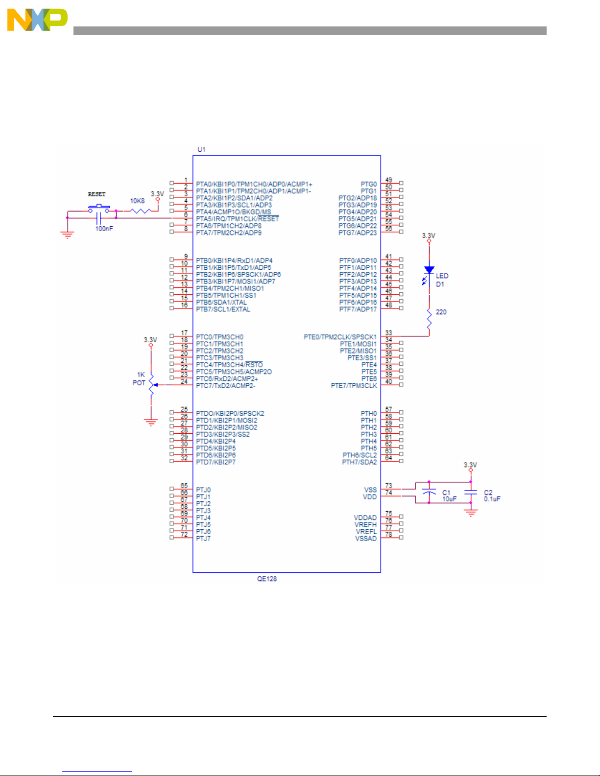
Using the Analog Comparator (ACMP) for the QE Microcontrollers
7.2.2 Hardware Implementation
This project is developed using the EVBQE128 STARTER KIT. Extra hardware is needed. A variable
resistor of 1 kΩ is required. One terminal of the potentiometer (POT) is connected to 3.3 V and the other
terminal is connected to the ground. When the POT varies, the voltage in the center pin change. This pin
is the input for the PTC7 pin. Figure 7-2 shows the hardware configuration.
Figure 7-2. ACMP Hardware Implementation
This example is developed using the CodeWarrior IDE version 6.0 for the
HCS08 and V1 families. It is expressly made for the MCF51QE128 and
MC9S08QE128 (80-pin package). There may be changes needed in the
code to initialize another MCU.
7-4 Freescale Semiconductor
NOTE
QE128 Quick Reference User Guide, Rev. 1.0
Page 69

Using the Analog Comparator (ACMP) for the QE Microcontrollers
ACMP module can operate with two external inputs. This example code is
expressly made to configure the ACMP module to work using the internal
reference voltage.
The analog comparator circuit is designed to operate across a full range of
supply voltage. Please refer to the data sheet of the device. You can find it
at www.freescale.com.
Figure 7-2, shows the hardware connections used for the ACMP project, for
detailed information about the MCU supply voltages needed, please refer to
the Pins and Connections chapter in the Reference Manual (MC9S08QE128
or MCF51QE128). It can be found at www.freescale.com.
7.3 ACMP project for Demo board
7.3.1 Code Example and Explanation
These example codes are available from the Freescale Web site www.freescale.com.
This section explains the differences of codes using an EVB and Demo board. The codes are the same.
The project ACMP .mcp implements the ACMP function, selecting a rising- or falling-edge event to trigger
hardware interrupts. The main functions are:
• main — Endless loop waiting for the ACMP interrupt to occur.
• MCU_Init – MCU initialization, watchdog disable and the ACMP clock module enabled.
• GPIO_Init – Configure PTC0 pin as output.
• ACMP_Init – ACMP module configuration.
• ACMP_ISR — Toggles a LED after a rising or falling edge event occurs.
This is the General Purpose Input/Output configuration. These code lines configure the direction for P TC
port. Only six LEDs from the demo board are connected to the PTC port. The other two LEDs are
connected to the E port. In this example only the PTC0 is configured as output in order to drive a LED.
void GPIO_Init(void) {
PTCDD = 0x01; // Configure PTC port as output
PTCD = 0x00; // Put 0's in PTC port
}
NOTE
This is the analog comparator interrupt service routine. Every time an
interrupt is detected, this routine toggles a LED (PTC0). The
V ectorNumber_Vacmpx can be replaced by the interrupt vector number, this
depends if the MCU is S08 or V1. Using this example makes the code fully
compatible for either MCU.
void interrupt VectorNumber_Vacmpx ACMP_ISR(void) {
// ACMP vector address = 20 (S08)
// ACMP vector address = 82 (V1)
ACMP2SC_ACF = 1; // Clear ACMP flag */
PTCD_PTCD0 ^= 1; // Toggles PTC0 */
Freescale Semiconductor 7-5
QE128 Quick Reference User Guide, Rev. 1.0
Page 70

Using the Analog Comparator (ACMP) for the QE Microcontrollers
}
7.3.2 Hardware Inplementation
This project is developed using the demo board. Extra hardware is needed. A variable resistor of 1 kΩ is
required. One terminal of the POT is connected to 3.3 V and the other terminal is connected to the ground.
In this configuration when POT varies, the voltage in the center pin changes, this pin is the input for P TC7
pin. Figure 7-3 shows the hardware configuration.
Figure 7-3. ACMP Hardware Implementation
This example is developed using the CodeWarrior IDE version 6.0 for the
HCS08 and V1 families. It is expressly made for the MCF51QE128 and
MC9S08QE128 (64-pin package). There may be changes needed in the
code to initialize another MCU.
7-6 Freescale Semiconductor
NOTE
QE128 Quick Reference User Guide, Rev. 1.0
Page 71

Using the Analog Comparator (ACMP) for the QE Microcontrollers
ACMP module can operate with two external inputs. This example code is
expressly made to configure the ACMP module to work using the internal
reference voltage.
The analog comparator circuit is designed to operate across a full range of
supply voltage. Please refer to the data sheet of the device. Y ou can also find
it at www.freescale.com.
Figure 7-3, shows the hardware connections used for the ACMP project, for
detailed information about the MCU supply voltages needed, please refer to
the Pins and Connections chapter the Reference Manual (MC9S08QE128 or
MCF51QE128). It can also be found at www.freescale.com.
Freescale Semiconductor 7-7
QE128 Quick Reference User Guide, Rev. 1.0
Page 72

Using the Analog Comparator (ACMP) for the QE Microcontrollers
7-8 Freescale Semiconductor
QE128 Quick Reference User Guide, Rev. 1.0
Page 73

Chapter 8
Using the Analog to Digital Converter (ADC) for the QE
Microcontrollers
8.1 Overview
This is a quick reference for using a 12-bit analog-to-digital converter (ADC) module for the QE family
microcontrollers (MCUs). Basic information about the functional description and configuration options
are provided. The following example may be modified to suit an application. The ADC project is made for
the MC9S08QE128 and MCF51QE128 MCUs.
ADC Quick Reference
For specific pin control registers and bits on the device, please refer to the
reference manual (MC9S08QE128 or MCF51QE128). It can be found at
www.freescale.com.
ADCSC1 COCO AIEN ADCO ADCH
Module configuration:
ACME – conversion complete flag ADCO – continuous conversion enable
AIEN – Interrupt enable ADCH– output pin enable.
ADCSC2 ADACT ADTRG ACFE ACFGT
Module configuration:
ADACT – conversion active. ADTRG – conversion trigger select
ACFE – compare function enable. ACFGT– compare function greater than
enable
ADCRH ADR11 ADR10 ADR9 ADR8
Result of ADC conversion:
ADR11-ADR8 – contains the upper four bits of the result of a 12-bit conversion
ADCRL ADR7 ADR6 ADR5 ADR4 ADR3 ADR2 ADR1 ADR0
Result of ADC conversion:
ADR7-ADR0 – contains the eight bits of the result of a 12-bit, 10-bit or 8-bit
conversion
ADCCVH ADCV11 ADCV10 ADCV9 ADCV8
Compare value:
ADCV11-ADCV8 – contains the upper four bits of the 12-bit compare value.
ADCCVL ADCV7 ADCV6 ADCV5 ADCV4 ADCV3 ADCV2 ADCV1 ADCV0
Freescale Semiconductor 8-1
QE128 Quick Reference User Guide, Rev. 1.0
Page 74

Using the Analog to Digital Converter (ADC) for the QE Microcontrollers
Compare value.
ADCV7-ADCV0 – contains the lower eight bits of the 12-bit, 10-bit or 8-bit
compare value
ADCCFG ADLPC ADIV ADLSMP MODE ADICLK
ADLPC – Low Power configuration MODE – Conversion mode Selection
ADIV – Clock divide select ADICLK – Input clock select.
ADLSMP – Long sample time
configuration.
APCTL1 ADPC7 ADPC6 ADPC5 ADPC4 ADPC3 ADPC2 ADPC1 ADPC0
Pin Control: ADC or I/O controlled
ADPC7-ADPC0 – These bits are used to disable the I/O port control of the
MCU. For specific information visit www.freescale.com and search for the
reference manual MC9S08QE128 or MCF51QE128 MCUs.
APCTL2 ADPC15 ADPC14 ADPC13 ADPC12 ADPC11 ADPC10 ADPC9 ADPC8
Pin Control: ADC or I/O controlled
ADPC15-ADPC8 – These bits are used to disable the I/O port control of the
MCU. For specific information visit www.freescale.com and search for the
reference manual MC9S08QE128 or MCF51QE128 MCUs.
APCTL3 ADPC23 ADPC22 ADPC21 ADPC20 ADPC19 ADPC18 ADPC17 ADPC16
Pin Control: ADC or I/O controlled
ADPC23-ADPC16 – These bits are used to disable the I/O port control of the
MCU. For specific information visit www.freescale.com and search for the
reference manual MC9S08QE128 or MCF51QE128 MCUs.
The QE128 MCUs have a 12-bit analog-to-digital succesive-approximation converter which is the ADC.
It can be configured with a 12-bit, 10-bit or 8-bit resolution. These are some options for the user:
• Three different resolutions: 12-bit, 10-bit and 8-bit.
• Two different types of conversions: single or continuous conversion.
• Selectable ADC clock frequency: include a bus clock preescaler.
• Automatic compare with interrupt for less-than, grater-than or equal-to, programmable value.
• Configurable sample time and conversion speed/power.
8.2 ADC project for EVB
8.2.1 Code Example and Explanation
This example code is available from the Freescale Web site www.freescale.com.
The following examples describe the initialization code for the 12-bit ADC module using the
interrupt-based approach, 8-bit resolution, and continuous-sample mode.
The zip file contains the following functions:
• main — Endless loop waiting for the ADC interrupt to occur.
8-2 Freescale Semiconductor
QE128 Quick Reference User Guide, Rev. 1.0
Page 75

Using the Analog to Digital Converter (ADC) for the QE Microcontrollers
• MCU_Init – MCU initialization, watchdog disable and the ADC clock module enabled.
• GPIO_Init – Configure PTE port as output.
• ADC_Init – ADC module configuration.
• ADC_ISR — The data obtained by ADC module is display on PTE port.
This section consists of varying the potentiometer that also varies the voltage and is connected to the ADC
channel 0. The obtained data is displayed in an 8 LEDs array connected to the P TE port. The ADC module
is configured in continuous conversion mode. The MCU is interrupted constantly and within the ISR the
obtained data is displayed on the PTE port.
The code below executes the instructions to disable the watchdog, enable the Reset option and backgroud
pin. The system option register 1 (SOPT1) is used to configure the MCU. The SCGC1 and SCGC2 are
registers used for power saving consumption, here the bus clock to peripherals can be enabled or disabled.
In this example only the bus clock to the ADC module is active. The clocks to the other peripherals are
disabled.
void MCU_Init(void) {
SOPT1 = 0x23; // Watchdog disabled. Stop Mode Enabled. Background Pin
// enabled. RESET pin enabled
SCGC1 = 0x10; // Bus Clock to the ADC module is enabled
SCGC2 = 0x00; // Disable Bus clock to unused peripherals
}
This is the General Purpose Input/Output configuration. These code lines configure the directions for the
PTE port. The eight LEDs are connected to the PTE port; therefore the PTE port is configured as output.
void GPIO_Init(void) {
PTEDD = 0xFF; // Configure PTE port as output
PTED = 0x00; // Put 0's in PTE port
}
This is the initialization code for the analog-to-digital converter used for the QE MCU. This application
uses the ADC module channel 0. The module is configured in continuous conversion mode and an 8-bit
resolution.
void ADC_Init (void) {
ADCSC1 = 0x20; // Interrupt disable. Continuous conversion and channel 0
// active
ADCSC2 = 0x00; // Software trigger selected
ADCCFG = 0x30; // Input clock/2. Long Sample time configuration. 8-bit
// conversion
APCTL1 = 0x00; // ADC0 pin disable
}
This is the main function, above are the described called functions, and all the interrupts are enabled. The
ADC interrupt can be serviced.
void main(void) {
MCU_Init(); // initializes the MCU
GPIO_Init(); // initializes GPIO
ADC_Init(); // Function that initializes the ADC module
EnableInterrupts; // enable interrupts
ADCSC1_AIEN = 1; // Enable ADC interrupt
APCTL1_ADPC0 = 1; // Select the channel for ADC input
for(;;) {
} // loop forever
Freescale Semiconductor 8-3
QE128 Quick Reference User Guide, Rev. 1.0
Page 76
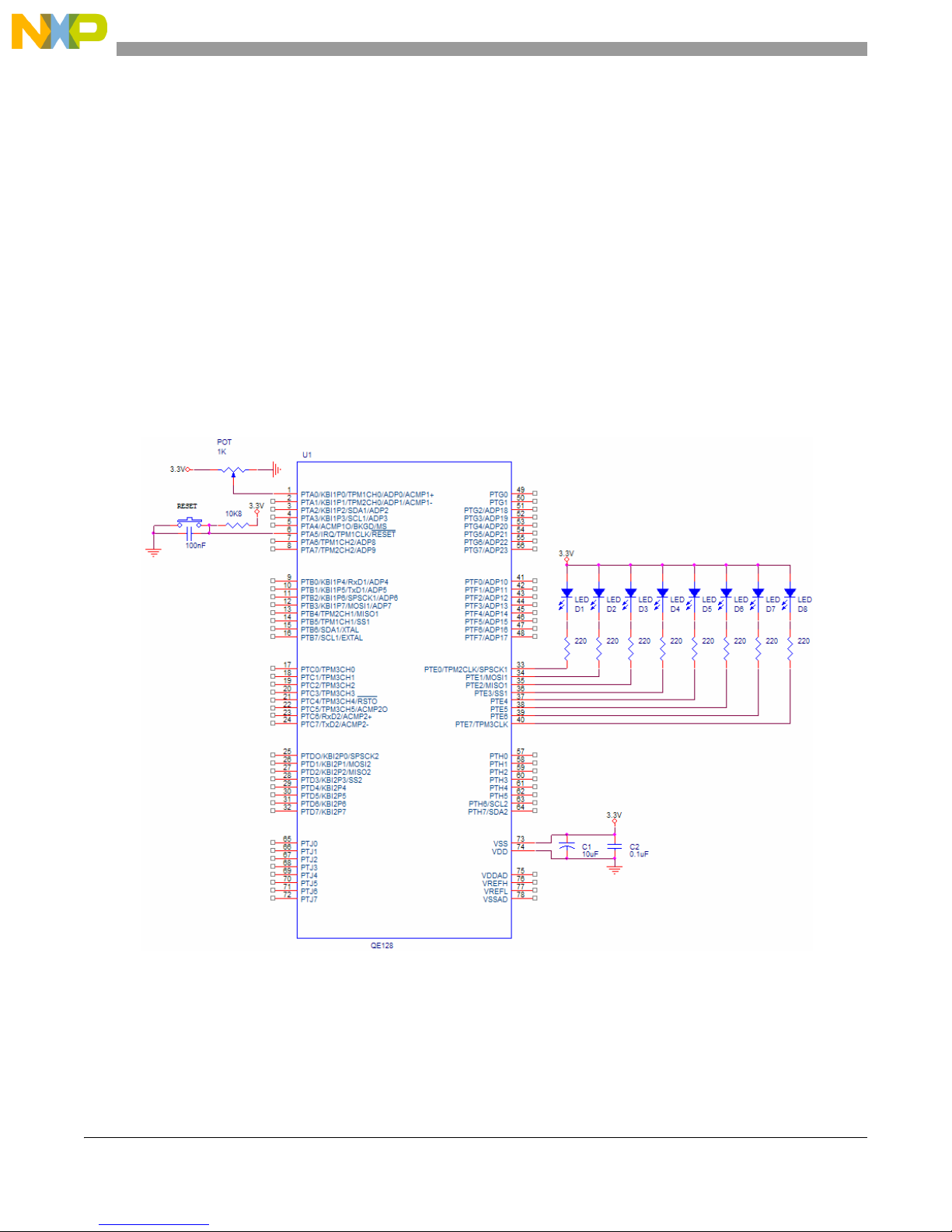
Using the Analog to Digital Converter (ADC) for the QE Microcontrollers
// please make sure that you never leave this function
}
NOTE
This is the analog-to-digital converter interrupt service routine. Every time
an interrupt is detected, this routine displays the converted value in PTE
port. The VectorNumber_Vadc can be replaced by the interrupt vector
number, this depends if the MCU is S08 or V1. Using this example makes
the code fully compatible for either MCU.
void interrupt VectorNumber_Vadc ADC_ISR(void) {
// ADC vector address = 19 (S08)
// ADC vector address = 81 (V1)
PTED = ADCRL; // Move the adquired ADC value to PTE port
}
8.2.2 Hardware Implementation
Figure 8-1. ADC Hardware Implementation.
8-4 Freescale Semiconductor
QE128 Quick Reference User Guide, Rev. 1.0
Page 77

Using the Analog to Digital Converter (ADC) for the QE Microcontrollers
NOTE
This example is developed using the CodeWarrior version 6.0 for the
HCS08 and V1 families. It is expressly made for the MCF51QE128 and
MC9S08QE128 (80-pin package). There may be changes needed in the
code to initialize another MCU.
Figure 8-1, shows the hardware connections used for the ADC project, for
detailed information about the MCU hardware needed, please refer to the
Pins and Connections chapter in the Reference Manual. It can be found at
www.freescale.com.
8.3 ADC project for Demo board
8.3.1 Code Example and Explanation
This example code is available from the Freescale Web site www.freescale.com.
This section explains the differences of codes using an EVB and Demo board. The codes are the same.
The project file contains the following functions:
• Main — Endless loop waiting for the ADC interrupt to occur.
• MCU_Init – MCU initialization, watchdog disable and the ADC clock module enabled.
• GPIO_Init – Configure PTC0 to PTC5, PTE6 and PTE7 as as outputs.
• ADC_Init – ADC module configuration.
• ADC_ISR — The data obtained by the ADC module is displayed on P TC0 to P TC5 pins, P TE6 and
PTE7 pins.
This is the General Purpose Input/Output configuration. These code lines configure the direction for the
PTC port. Only six LEDs from the demo board are connected to the PTC port. The other two LEDs are
connected to port E. In this example the P TC0 to P TC5, and P TE6, P TE7 are configured as outputs in order
to drive LEDs.
void GPIO_Init(void) {
PTCDD = (UINT8) (PTCD | 0x3F); // Configure PTC0-PTC5 as outputs
PTEDD = (UINT8) (PTED | 0xC0); // Configure PTE6 and PTE7 pins as outputs
PTCD = 0x3F; // Put 1's in port C in order to turn off the LEDs
PTED = 0xC0; // Put 1's in port E in order to turn off the LEDs
}
NOTE
This is the ADC interrupt service routine. Every time an interrupt is
detected, this routine displays the converted value in eight LEDs. The
VectorNumber_Vadc can be replaced by the interrupt vector number, this
depends if the MCU is S08 or V1. Using these example makes the code fully
compatible for either MCU.
void interrupt VectorNumber_Vadc ADC_ISR(void) {
// ADC vector address = 19 (S08)
// ADC vector address = 81 (V1)
Freescale Semiconductor 8-5
QE128 Quick Reference User Guide, Rev. 1.0
Page 78

Using the Analog to Digital Converter (ADC) for the QE Microcontrollers
UINT8 temp; // Create a temp variable used for further operations
temp = ~ADCRL; // Negate the ADC converted value because is going to be display
// on the LEDs (The LEDs turn on with 0's)
PTED = (UINT8) (temp & 0xC0); // Move the adquired ADC value to port E
PTCD = (UINT8) (temp & 0x3F); // Move the adquired ADC value to port C
}
8.3.2 Hardware Implementation
This example is developed using the CodeWarrior version 6.0 for the
HCS08 and V1 families. It is expressly made for the MCF51QE128 and
MC9S08QE128 (64-pin package). There may be changes needed in the
code to initialize another MCU.
8-6 Freescale Semiconductor
Figure 8-2. ADC Hardware Implementation
NOTE
QE128 Quick Reference User Guide, Rev. 1.0
Page 79

Using the Analog to Digital Converter (ADC) for the QE Microcontrollers
Figure 8-2, shows the hardware connections used for the ADC project, for
detailed information about the MCU hardware needed, please refer to the
Pins and Connections chapter in the Reference Manual. It can be found at
www.freescale.com.
Freescale Semiconductor 8-7
QE128 Quick Reference User Guide, Rev. 1.0
Page 80

Using the Analog to Digital Converter (ADC) for the QE Microcontrollers
8-8 Freescale Semiconductor
QE128 Quick Reference User Guide, Rev. 1.0
Page 81

Chapter 9
Using the Real Time Counter (RTC) for the QE
Microcontrollers
9.1 Overview
This is a quick reference for using the real time counter (R TC) module for the QE family microcontrollers
(MCUs). Basic information about the functional description and configuration options are provided. The
following example may be modified to suit an application. The RTC project is made for the
MC9S08QE128 and MCF51QE128 MCUs.
The R TC module can be used to generate a hardware interrupt at fixed periodic rate. The RTC module in
QE MCU has three clock sources, the 1 kHz internal clock, the 32 kHz internal clock and an external clock.
There are different periods of time that can be used to interrupt the MCU. Please refer the reference manual
for specific times. It can be found at www.freescale.com.
RTC Quick Reference
RTCSC RTIF RTCLKS RTIE RTCPS
Module Configuration:
RTIF - Real-Time Interrupt flag IRTIE - Real-Time Interrupt Enable
RTCLKS - Real-Time Clock Source Select RTCPS - Real-Time clock prescaler select
RTCCNT RTCCNT
RTCCNT - It contains the value of the current RTC count
RTCMOD RTCMOD
RTCMOD - RTC Modulo
9.2 RTC project for EVB
9.2.1 Code Example and Explanation
This example code is available from the Freescale Web site www.freescale.com.
The zip file contains the following functions:
• main — Endless loop waiting for the RTC interrupt to occur.
• MCU_Init – MCU initialization, watchdog disable and the RTC clock module enabled.
• GPIO_Init – Configure PTE port as output.
• RTC_Init – RTC module configuration.
• RTC_ISR — Toggles PTE port .
Freescale Semiconductor 9-1
QE128 Quick Reference User Guide, Rev. 1.0
Page 82

Using the Real Time Counter (RTC) for the QE Microcontrollers
The following example describes the initialization code for the R TC module. This example shows how to
generate an RTC using 1 kHz of internal reference. Port E toggles every time an interrupt is generated
which is every second.
The code below executes the instructions to disable the watchdog, enable the Reset option and backgroud
pin. The system option register 1 (SOPT1) is used to configure the MCU. The SCGC1 and SCGC2 are
registers used for power saving consumption, here the bus clock to peripherals can be enabled or disabled.
In this example only the bus clock to the RTC module is active. The clocks to the other peripherals are
disabled.
void MCU_Init(void) {
SOPT1 = 0x23; // Watchdog disabled. Stop Mode Enable. Background Pin
// enable. RESET pin enable
SCGC1 = 0x00; // Disable Bus clock to unused peripherals
SCGC2 = 0x04; // Bus Clock to the RTC module is enable
}
This is the general purpose Input/Output (GPIO) configuration. These code lines configure the directions
for the PTE ports. The eight LEDs are connected to the PTE port; therefore the PTE port is configured as
output.
void GPIO_Init(void) {
PTEDD = 0xFF; // Configure PTE port as output
PTED = 0x00; // Put 0's in PTE port
}
This is the initialization code for the Real-Time clock module used for the QE MCU. This application
generates an interrupt every second. Within the interrupt service routine a PTE port is toggled.
void RTC_Init (void) {
RTCSC = 0x0F; // RTCPS configure prescaler period every 1s
RTCMOD = 0x00; // RTCMOD configure to interrupt every 1s
}
This is the main function, above are the described called functions, all the interrupts are enabled. The R TC
interrupt can be detected.
void main(void) {
MCU_Init(); // Function that initializes the MCU
GPIO_Init(); // Function that initializes the Ports of the MCU
RTC_Init(); // Function that initializes the RTC module
EnableInterrupts; // enable interrupts
RTCSC_RTIE = 1; // Enable RTC interrupt
} // loop forever
// please make sure that you never leave this function
}
NOTE
This is the RTC interrupt service routine. Every second an interrupt is
generated this routine toggles a PTE port. The VectorNumber_Vrtc can be
replaced by the interrupt vector number, this depends if the MCU is S08 or
V1. Using these example makes the code fully compatible for either MCU.
void interrupt VectorNumber_Vrtc RTC_ISR(void) {
9-2 Freescale Semiconductor
QE128 Quick Reference User Guide, Rev. 1.0
Page 83

Using the Real Time Counter (RTC) for the QE Microcontrollers
// RTC vector address = 24 (S08)
// RTC vector address = 86 (V1)
RTCSC = RTCSC | 0x80; // Clear the RTC flag
PTED ^= 0xFF; // Toggles Port E
}
9.2.2 Hardware Implementation
Figure 9-1. RTC Hardware Implementation.
This example is developed using the CodeWarrior IDE version 6.0 for the
HCS08 and V1 families. It is expressly made for the MCF51QE128 and
MC9S08QE128 (80-pin package). There may be changes needed in the
code to initialize another MCU.
Figure 9-1, shows the hardware connections used for the RTC project, for
detailed information about the MCU hardware needed, please refer to the
Pins and Connections chapter in the Reference Manual. It can be found at
www.freescale.com.
Freescale Semiconductor 9-3
NOTE
QE128 Quick Reference User Guide, Rev. 1.0
Page 84

Using the Real Time Counter (RTC) for the QE Microcontrollers
9.3 RTC project for Demo board
9.3.1 Code Example and Explanation
This example code is available from the Freescale Web site www.freescale.com.
This section explains the differences of codes using the EVB and Demo board. The codes are the same.
The project file contains the following functions:
• Main — Endless loop waiting for the RTC interrupt to occur.
• MCU_Init – MCU initialization, watchdog disable and the RTC clock module enabled.
• GPIO_Init – Configure PTC0 pin as output.
• RTC_Init – RTC module configuration.
• RTC_ISR — Toggles PTC0 pin .
This is the general purpose Input/Output (GPIO) configuration. These code lines configure the direction
for the P TC port. Only six LEDs from the demo board are connected to the P TC port. The others two LEDs
are connected to port E. In this example PTC0 is configured as output in order to drive a LED.
void GPIO_Init(void) {
PTCDD = 0x01; // Configure PTC0 as output
PTCD = 0x01; // Put 1 in PTC0 to turn off the LED
}
NOTE
This is the RTC interrupt service routine. Every second an interrupt is
generated this routine toggles a PTE port. The VectorNumber_Vrtc can be
replaced by the interrupt vector number, this depends if the MCU is S08 or
V1. Using this example makes the code fully compatible for either MCU.
void interrupt VectorNumber_Vrtc RTC_ISR(void) {
// RTC vector address = 24 (S08)
// RTC vector address = 86 (V1)
RTCSC = RTCSC | 0x80; // Clear the RTC flag
PTCD_PTCD0 ^= 1; // Toggles PTC0 pin
}
9-4 Freescale Semiconductor
QE128 Quick Reference User Guide, Rev. 1.0
Page 85

9.3.2 Hardware Implementation
Using the Real Time Counter (RTC) for the QE Microcontrollers
Figure 9-2. RTC Hardware Implementation.
This example is developed using the CodeWarrior IDE version 6.0 for the
HCS08 and V1 families. It is expressly made for the MCF51QE128 and
MC9S08QE128 (64-pin package). There may be changes needed in the
code to initialize another MCU.
Freescale Semiconductor 9-5
NOTE
QE128 Quick Reference User Guide, Rev. 1.0
Page 86

Using the Real Time Counter (RTC) for the QE Microcontrollers
Figure 9-2, shows the hardware connections used for the RTC project, for
detailed information about the MCU hardware needed, please refer to the
Pins and Connections chapter in the Reference Manual. It can be found at
www.freescale.com.
9-6 Freescale Semiconductor
QE128 Quick Reference User Guide, Rev. 1.0
Page 87

Chapter 10
Using the Serial Communications Interface (SCI) for the QE
Microcontrollers
10.1 Overview
This is a quick reference for using the serial communication interface (SCI) module for the QE family
microcontrollers (MCUs). Basic information about the functional description and configuration options
are provided. The following example may be modified to suit an application. The SCI project is made for
the MC9S08QE128 and MCF51QE128 MCUs.
10.2 SCI project for EVB
10.2.1 Code Example and Explanation
This example code is available from the Freescale Web site www.freescale.com.
The zip file contains the following functions:
• main — Endless loop waiting for the SCI interrupt to occur.
• MCU_Init – MCU initialization, watchdog disable and the SCI clock module enabled.
• GPIO_Init – Configure PTE port as output.
• SCI_Init – SCI module configuration.
• SCI_RX_ISR — The data obtained by SCI module is displayed on the PTE port and the character
“1” is sent by SCI.
The following example describes the initialization code for the SCI module. This example configures the
serial communications interface at 9600bps, in an 8-bit mode. The MCU waits for an interrupt, once an
interrupt is detected the received data is displayed on the PTE port and then the character “1” is sent by
SCI. The SCI module uses interrupts to handle transmition, reception and errors events, for this example
reception interrupt is used.
The code below executes the instructions to disable the watchdog, enable the Reset option and backgroud
pin. The System Option Register 1 (SOPT1) is used to configure the MCU. The SCGC1 and SCGC2 are
registers used for saving power consumption, here the bus clock to peripherals can be enabled or disabled.
In this example only the bus clock to the SCI module is active. The clocks to the other peripherals are
disabled.
void MCU_Init(void) {
SOPT1 = 0x23; // Watchdog disabled. Stop Mode Enabled. Background Pin
// enable. RESET pin enable
SCGC1 = 0x01; // Bus Clock to the SCI1 module is enabled
SCGC2 = 0x00; // Disable Bus clock to unused peripherals
QE128 Quick Reference User Guide, Rev. 1.0
Freescale Semiconductor 10-1
Page 88

Using the Serial Communications Interface (SCI) for the QE Microcontrollers
}
This is the General Purpose Input/Output configuration. These code lines configure the directions for the
PTE ports. The eight LEDs are connected to the PTEport; therefore the PTE port is configured as output.
void GPIO_Init(void) {
PTEDD = 0xFF; // Configure PTE port as output
PTED = 0x00; // Put 0's in PTE port
}
This is the initialization code for Serial Communications Interface module used for the QE MCU. This
application configures the SCI module in an 8-bit mode, normal operation, and a baud rate of 9600 bps.
To reach 9600 bps the Baud Rate Modulo Divisor and the clock source must be configured. For this
example the used clock source is at its default of 4 MHz. The Baud Rate Modulo Divisor needs to be at 26
to obtain 9600 bps.
void SCI_Init (void) {
SCI1C1 = 0x00; // 8-bit mode. Normal operation
SCI1C2 = 0x2C; // Receiver interrupt enabled. Transmitter and receiver enabled
SCI1C3 = 0x00; // Disable all errors interrupts
SCI1BDL = 0x1A; // This register and the SCI1BDH are used to configure the SCI baud rate
SCI1BDH = 0x00; // BUSCLK 4MHz
// Baud rate = -------------------- = ------------ = 9600bps
} // [SBR12:SBR0] x 16 26 x 16
This is the main function, the above described functions are called, and all the interrupts are enabled. The
SCI_Rx interrupt can be detected.
void main(void) {
MCU_Init(); // Function that initializes the MCU
GPIO_Init(); // Function that initializes the Ports of the MCU
SCI_Init(); // Function that initializes the SCI module
EnableInterrupts; // enable interrupts
for(;;) {
} // loop forever
// please make sure that you never leave this function
}
This is the SCI service routine. Every time a SCI interrupt is detected, the received data is displayed on the
P TE port and the character “1” is sent by SCI. The V ectorNumber_Vsci1rx can be replaced by the interrupt
vector number, this depends if the MCU is S08 or V1. Using this example makes the code fully compatible
for either MCU.
void interrupt VectorNumber_Vsci1rx SCI_RX_ISR(void) {
// SCI vector address = 15 (S08)
// SCI vector address = 77 (V1)
SCI1S1_RDRF = 0; // Receive interrupt disable
PTED = SCI1D; // Display on PTE the received data from SCI
while (SCI1S1_TDRE == 0); // Wait for the transmitter to be empty
SCI1D = '1'; // Send a character by SCI
}
10-2 Freescale Semiconductor
QE128 Quick Reference User Guide, Rev. 1.0
Page 89

Using the Serial Communications Interface (SCI) for the QE Microcontrollers
10.2.2 Hardware Implementation
Figure 10-1. SCI Hardware Implementation
NOTE
This example is developed using the CodeWarrior IDE version 6.0 for the
HCS08 and V1 famies. It is expressly made for the MCF51QE128 and
MC9S08QE128 (80-pin package). There may be changes needed in the
code to initialize another MCU.
Figure 10-1, shows the hardware connections used for the SCI project, for
detailed information about the MCU power supply, please refer to the Pins
and Connections chapter in the Reference Manual. It can be found at
www.freescale.com.
The SCI.mcp project needs to work with the hyperterminal program. The hyperterminal is configured to
the following characteristics:
• 9600bps baud rate
• 8-bit mode
• No parity checked
• 1 stop bit
• No flow control
Freescale Semiconductor 10-3
QE128 Quick Reference User Guide, Rev. 1.0
Page 90

Using the Serial Communications Interface (SCI) for the QE Microcontrollers
Press any key and the character “1” appears.
10.3 SCI project for Demo board
10.3.1 Code Example and Explanation
This example code is available from the Freescale Web site www.freescale.com.
This section explains the differences of codes used in the EVB and Demo board. The codes are the same.
The project file contains the following functions:
• main — Endless loop waiting for the SCI interrupt to occur.
• MCU_Init – MCU initialization, watchdog disable and the SCI clock module enabled.
• GPIO_Init – Configure PTC0-PTC5, PTE6 and PT7 as outputs.
• SCI_Init – SCI module configuration.
• SCI_RX_ISR — The data obtained by SCI module is display on eight LEDs and the character “1”
is send it by SCI.
This is the General Purpose Input/Output configuration. These code lines configure the direction for the
PTC port. Only six LEDs from the demo board are connected to the PTC port. The other two LEDs are
connected to the E port. In this example P TC0 to P TC5, and P TE6, P TE7 are configured as outputs in order
to drive LEDs.
void GPIO_Init(void) {
PTCDD = (UINT8) (PTCD | 0x3F); // Configure PTC0-PTC5 as outputs
PTEDD = (UINT8) (PTED | 0xC0); // Configure PTE6 and PTE7 pins as outputs
PTCD = 0x3F; // Put 1's in port C in order to turn off the LEDs
PTED = 0xC0; // Put 1's in port E port in order to turn off the LEDs
}
NOTE
This is the SCI service routine. Every time an SCI interrupt is detected, the
received data is displayed on eight LEDs and the character “1” is sent by
SCI. The VectorNumber_Vsci1rx can be replaced by the interrupt vector
number, this depends if the MCU is S08 or V1. Using this example makes
the code fully compatible for either MCU.
void interrupt VectorNumber_Vsci1rx SCI_RX_ISR(void) {
// SCI vector address = 15 (S08)
// SCI vector address = 77 (V1)
UINT8 temp;
SCI1S1_RDRF = 0; // Receive interrupt disable
temp = SCI1D; // Store the recieve value on temp variable
PTED = (UINT8) (temp & 0xC0); // Move the received value to port E
PTCD = (UINT8) (temp & 0x3F); // Move the received value to port C
while (SCI1S1_TDRE == 0); // Wait for the transmitter to be empty
SCI1D = '1'; // Send a character by SCI
}
QE128 Quick Reference User Guide, Rev. 1.0
10-4 Freescale Semiconductor
Page 91

Using the Serial Communications Interface (SCI) for the QE Microcontrollers
10.3.2 Hardware Implementation
Figure 10-2. SCI Hardware Implementation.
NOTE
This example is developed using the CodeWarrior IDE version 6.0 for the
HCS08 and V1 families. It is expressly made for the MCF51QE128 and
MC9S08QE128 (64-pin package). There may be changes needed in the
code to initialize another MCU.
Figure 10-2, shows the hardware connections used for the SCI project, for
detailed information about the MCU power supply, please refer to the Pins
and Connections chapter in the Reference Manual. It can also be found at
www.freescale.com.
The SCI.mcp project needs to work with the hyperterminal program. The hyperterminal is configured to
the following characteristics:
• 9600bps baud rate
• 8-bit mode
• No parity checked
QE128 Quick Reference User Guide, Rev. 1.0
Freescale Semiconductor 10-5
Page 92

Using the Serial Communications Interface (SCI) for the QE Microcontrollers
• 1 stop bit
• No flow control
Press any key and the character “1” appears.
10-6 Freescale Semiconductor
QE128 Quick Reference User Guide, Rev. 1.0
Page 93

Chapter 11
Using the Serial Peripheral Interface (SPI) for the QE
Microcontrollers
11.1 Overview
This is a quick reference for using the serial peripheral interface (SPI) module for the QE family
microcontrollers (MCUs). Basic information about the functional description and configuration options
are provided. The following example may be modified to suit an application. The SPI project is made for
the MC9S08QE128 and MCF51QE128 MCUs.
SPI Quick Reference
Because there are two SPI modules on some devices, there may be two full sets of registers. In the
register names below, where there’s a small x, there would be a 1 or a 2 in your softwar e to
distinguish the registers that are on SPI1 from those on SPI2.
SPIxC1 SPIE SPE SPTIE MSTR CPOL CPHA SSOE LSBFE
Module configuration:
SPIE – SPI Interrupt Enable CPOL – Clock Polarity
SPE – SPI system Enable CPHA – Clock Phase
SPTIE – SPI transmit Interrupt Enable SSOE – Slave Select Output Enable
MSTR – Master/Slave Mode Select LSBFE – LSB First
SPIxC2 MODFEN BIDIROE SPISWAI SPC0
Module configuration:
MODFEN – Master Mode-Fault function Enable SPISWAI – SPI Stop in Wait mode
BIDIROE – Bidirectional mode Output Enable SPC0 – SPI Pin control 0
SPIxBR SPPR2 SPPR1 SPPR0 SPR2 SPR1 SPR0
SPPR[2:0] – SPI Baud Rate Prescaler Divisor SPR[2:0] – SPI Baud Rate Divisor
SPIxS SPRF SPTEF MODF
SPRF – SPI Read buffer full Flag MODF – Master Mode Fault Flag
SPTEF – SPI Transmit Buffer Empty Flag
SPIxD Bit 7 6 5 4 3 2 1 Bit 0
Data buffer
11.2 SPI project for EVB
11.2.1 Code Example and Explanation
This example code for Master and Slave project is available from the Freescale Web site
www.freescale.com.
Freescale Semiconductor 11-1
QE128 Quick Reference User Guide, Rev. 1.0
Page 94

Using the Serial Peripheral Interface (SPI) for the QE Microcontrollers
SS
SS
SS
()
)(Pr
4
625.15
Dividerescaler
MHz
kHz =
256
625.15
4
=
kHz
MHz
11.2.1.1 SPI Master Project
The project SPI_Master configures the SPI module in master mode. The main functions are:
• main — A byte is sent by SPI.
• MCU_Init – MCU initialization, watchdog disable and the SPI clock module enabled.
• GPIO_Init – Configure PTE port as output, configure PTD4 as output ( signal).
• SPI_Init – SPI module configuration.
• SPI_ISR — Clear module flags.
The following example describes the initialization code for the SPI module in master mode. Two boards
need to be connected. One board is configured as master, the other one works as slave. The firmware
configures the MCU as master and sends a count of 0 to 255 to the slave using the SPI module.
The code below executes the instructions to disable the watchdog, enable the Reset option and backgroud
pin. The System Option Register 1 (SOPT1) is used to configure the MCU. The SCGC1 and SCGC2 are
registers used for power saving consumption, here the bus clock to peripherals can be enabled or disabled.
In this example only the bus clock to the SPI2 module is active. The clocks to the other peripherals are
disabled.
void MCU_Init(void) {
SOPT1 = 0x23; // Watchdog disable. Stop Mode Enable. Background Pin
// enable. RESET pin enable
SCGC1 = 0x00; // Disable Bus clock to unused peripherals
SCGC2 = 0x02; // Bus Clock to the SPI2 module is enabled
}
This is the General Purpose Input/Output configuration. These code lines configure the pin directions for
the P TD port. The SPI protocol can communicate various slaves with one master. To communicate with a
specific slave the signal must be low. The P TD3 pin is configured as output and the signal must be
changed by software using a GPIO.
void GPIO_Init(void) {
PTDDD = 0x04; // The SS signal must be generated by software using a GPIO
PTEDD = 0xFF; // Configure PTE port as output
PTED = 0x00; // Put 0's in PTE port
}
This is the initialization code for Serial Peripheral Interface module used for the QE MCU. This
application configures the SPI module to work in master mode. The different pins are used for data input
and data output. To obtain a 15.625KHz bit rate it is necessary to do the following calculations:
256 = (Prescaler Divisor) x (Clock Rate Divider)
256 = 8*32
11-2 Freescale Semiconductor
QE128 Quick Reference User Guide, Rev. 1.0
Page 95

Using the Serial Peripheral Interface (SPI) for the QE Microcontrollers
void SPI_Init (void) {
SPI2BR = 0x75; // Select the highest baud rate prescaler divisor and the
// highest baud rate divisor
SPI2C1 = 0xD0; // SPI Interrupt enable, system enable and master mode selected
SPI2C2 = 0x00; // Different pins for data input and data output
}
This is the main function, descibed above are the called functions, and all the interrupts are enabled.
Within the endless loop a byte is sent by SPI and the next byte is sent after a delay . For detailed information
about the SPI module, refer to the QE MCU reference manual. It can be found at www.freescale.com.
void main(void) {
UINT8 counter = 0;
MCU_Init(); // Function that initializes the MCU
GPIO_Init(); // Function that initializes the Ports of the MCU
SPI_Init(); // Function that initializes the SPI module
EnableInterrupts; // enable interrupts
for(;;) {
delay(60000); // Delay function
while (!SPI2S_SPTEF && !PTDD_PTDD3); // Wait until transmit buffer is empty
PTDD_PTDD3 = 0; // Slave Select set in low
SPI2D = counter; // Put in SPI buffer a data to send
PTED = counter; // Display the counter value on LEDs
counter++; // Increment counter
} // loop forever
// please make sure that you never leave this function
}
NOTE
This is the SPI interrupt service routine. This routine is used when a byte is
sent by the slave to the master.
void interrupt VectorNumber_Vspi2 SPI_ISR(void) {
// SPI interrupt vector number = 12 (S08)
// SPI interrupt vector number = 74 (V1)
UINT8 temp;
while (PTDD_PTDD0); // Wait for clock to return no default
PTDD_PTDD3 = 1; // Set Slave Select high
temp = SPI2S; // Clear register flag
temp = SPI2D; // Read data register to clear receive flag
}
11.2.1.2 SPI Slave Project
The project SPI_Slave configures the SPI module in slave mode. The main functions are:
• main — Waits for the SPI interrupt to occur.
• MCU_Init – MCU initialization, watchdog disable and the SPI clock module enabled.
• GPIO_Init – Configure PTE port as output.
• SPI_Init – SPI module configuration.
• SPI_ISR — Display the received data in PTE port
The firmware for this project is similar to the SPI_master project. The differences are, the device is
configured as slave and only Receives a byte and displays it on the PTE port.
Freescale Semiconductor 11-3
QE128 Quick Reference User Guide, Rev. 1.0
Page 96

Using the Serial Peripheral Interface (SPI) for the QE Microcontrollers
This is the initialization code for the SPI module used for the QE MCU. This application configures the
SPI module to work in slave mode.
void SPI_Init (void) {
SPI2BR = 0x75; // Select the highest baud rate prescaler divisor and the
// highest baud rate divisor
SPI2C1 = 0xC4; // SPI Interrupt enable, system enable and slave mode selected
SPI2C2 = 0x00; // Different pins for data input and data output
}
NOTE
This is the SPI interrupt service routine. This routine is used when a byte is
sent by the master to the slave.
void interrupt VectorNumber_Vspi2 SPI_ISR(void) {
UINT8 temp, buffer;
while (PTDD_PTDD0);
temp = SPI2S; // Clear register flag
buffer = SPI2D;// Read data register to clear receive flag
PTED = buffer;
}
For detailed information about the code, refer to the SPI_Slave project from the QRUG examples.
11-4 Freescale Semiconductor
QE128 Quick Reference User Guide, Rev. 1.0
Page 97
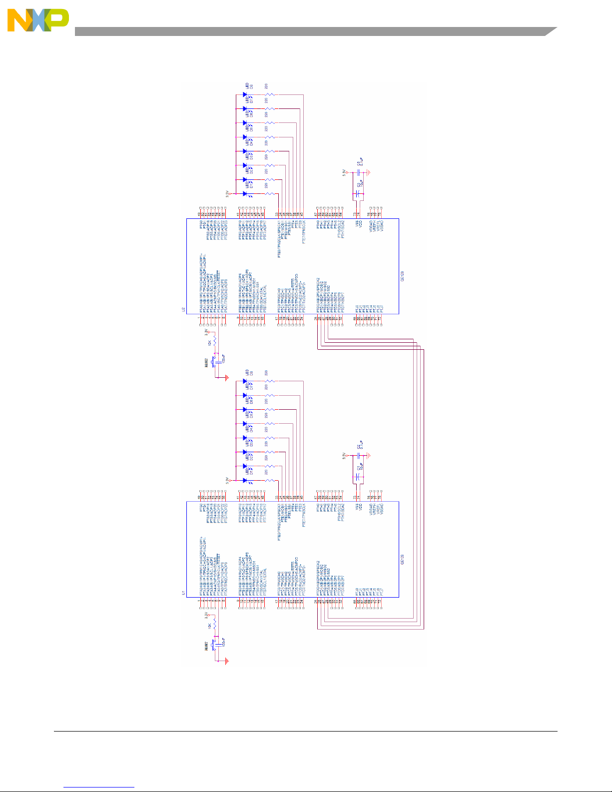
11.2.2 Hardware Implementation
Using the Serial Peripheral Interface (SPI) for the QE Microcontrollers
Figure 11-1. SPI Hardware Implementation.
Freescale Semiconductor 11-5
QE128 Quick Reference User Guide, Rev. 1.0
Page 98

Using the Serial Peripheral Interface (SPI) for the QE Microcontrollers
SS
NOTE
This example is developed using the CodeWarrior IDE version 6.0 for the
HCS08 and V1 families. It is expressly made for the MCF51QE128 and
MC9S08QE128 (80-pin package). There may be changes needed in the
code to initialize another MCU.
Figure 11-1, shows the hardware connections used for the SPI project, for
detailed information about the MCU hardware needed, please refer to the
Pins and Connections chapter in the Reference Manual. It can be found at
www.freescale.com.
11.3 SPI project for Demo board
11.3.1 Code Example and Explanation
This example code for the Master and Slave project is available from the Freescale Web site
www.freescale.com.
This Section explains the differences of codes used in the EVB and Demo board. The codes are the same.
11.3.1.1 SPI Master Project
The project SPI_Master configures the SPI module in master mode. The main functions are:
• main — A byte is sent by the SPI.
• MCU_Init – MCU initialization, watchdog disable and bus clock to the SPI clock module enabled.
• GPIO_Init – Configure P TC-P TC5, PTE6 and P TE7 pins as outputs, configure P TD4 as output (
signal).
• SPI_Init – SPI module configuration.
• SPI_ISR — Clear module flags.
This is the General Purpose Input/Output configuration. These code lines configure the pin directions for
the P TD port. The SPI protocol can communicate various slaves with one master. To communicate with a
specific slave the signal must be low. The PTD3 pin is configured as output and the signal must
be changed by software using a GPIO. These code lines configure the direction for the P TC port. Only six
LEDs from the demo board are connected to the PTC port. The other two LEDs are connected to the E
port. In this example the P TC0 to P TC6, and P TE6, P TE7 are configured as outputs in order to drive LEDs.
void GPIO_Init(void) {
PTDDD = 0x04; // The SS signal must be generated by software using a GPIO
PTCDD = (UINT8) (PTCD | 0x3F); // Configure PTC0-PTC6 as outputs
PTEDD = (UINT8) (PTED | 0xC0); // Configure PTE6 and PTE7 pins as outputs
PTCD = 0x3F; // Put 1's in port C in order to turn off the LEDs
PTED = 0xC0; // Put 1's in port E port in order to turn off the LEDs
}
This is the main function, described are the above functions are called, and all the interrupts are enabled.
Within the enless loop a byte is sent by SPI and the next byte is sent after a delay . For detailed information
about SPI module, refer to the QE MCU reference manual. It can be found at www.freescale.com.
11-6 Freescale Semiconductor
QE128 Quick Reference User Guide, Rev. 1.0
Page 99

Using the Serial Peripheral Interface (SPI) for the QE Microcontrollers
void main(void) {
UINT8 counter = 0;
MCU_Init(); // Function that initializes the MCU
GPIO_Init(); // Function that initializes the Ports of the MCU
SPI_Init(); // Function that initializes the SPI module
EnableInterrupts; // enable interrupts
for(;;) {
delay(60000); // Delay function
while (!SPI2S_SPTEF && !PTDD_PTDD3); // Wait until transmit buffer is empty
PTDD_PTDD3 = 0; // Slave Select set in low
SPI2D = counter; // Put in SPI buffer a data to send
PTED = (UINT8) (counter & 0xC0); // Move the adquired ADC value to port E
PTCD = (UINT8) (counter & 0x3F); // Move the adquired ADC value to port C
counter++; // Increment counter
} // loop forever
// please make sure that you never leave this function
}
11.3.1.2 SPI Slave Project
The project SPI_Slave configures the SPI module in slave mode. The main functions are:
• main — Waits for the SPI interrupt to occur.
• MCU_Init – MCU initialization, watchdog disable and the SPI clock module enabled.
• GPIO_Init – Configure PTE port as output.
• SPI_Init – SPI module configuration.
• SPI_ISR — Display the received data in eight LEDs
The firmware for this project is much similar to SPI_master project. The differences are that the device is
configured as slave and only Receives a byte and displays it on the PTE port.
This is the initialization code for Serial Peripheral Interface module used for the QE MCU. This
application configures the SPI module to work in slave mode.
void SPI_Init (void) {
SPI2BR = 0x75; // Select the highest baud rate prescaler divisor and the
// highest baud rate divisor
SPI2C1 = 0xC4; // SPI Interrupt enable, system enable and slave mode selected
SPI2C2 = 0x00; // Different pins for data input and data output
}
NOTE
This is the SPI interrupt service routine. This routine is used when a byte is
sent by the master to the slave.
void interrupt VectorNumber_Vspi2 SPI_ISR(void) {
UINT8 temp, buffer;
while (PTDD_PTDD0);
temp = SPI2S; // Clear register flag
buffer = ~SPI2D; // Read data register to clear receive flag
// on the LEDs (The LEDs turn on with 0's)
PTED = (UINT8) (temp & 0xC0); // Move the adquired ADC value to port E
PTCD = (UINT8) (temp & 0x3F); // Move the adquired ADC value to port C
Freescale Semiconductor 11-7
QE128 Quick Reference User Guide, Rev. 1.0
Page 100

Using the Serial Peripheral Interface (SPI) for the QE Microcontrollers
}
For detailed information about the code, refer to the SPI_Slave project from the QRUG examples.
11-8 Freescale Semiconductor
QE128 Quick Reference User Guide, Rev. 1.0
 Loading...