

Page 1

Freescale Semiconductor
User’s Guide
Document Number: MPC8313ERDBUG
Rev. 4, 02/2009
PowerQUICC™ MPC8313E Reference
Design Board (RDB)
The MPC8313E reference design board (RDB) is a system
featuring the PowerQUICC™ II Pro processor, which
includes a built-in security accelerator. This low-cost,
high-performance system solution consists of a printed
circuit board (PCB) assembly plus a s oft ware board support
package (BSP) distributed in a CD image. This BSP enables
the fastest possible time-to-market for development or
integration of applications including printer engines,
broadband gateways, no-new-wires home adapters/access
points, and home automation boxes.
This document describes the hardware features of the board
including specifications, block diagram, connectors,
interfaces, and hardware straps. It also describes the board
settings and physical connections needed to boot the
MPC8313E RDB. Finally, it considers the software shipped
with the platform.
When you finish reading this document, you should:
• Be familiar with the board layout
• Understand the default board configuration and your
board configuration options
• Know how to get started and boot the board
Contents
1. MPC8313E RDB Hardware . . . . . . . . . . . . . . . . . . . . 2
2. Board-Level Functions . . . . . . . . . . . . . . . . . . . . . . . . 7
3. Connectors, Jumpers, Switches, and LEDs . . . . . . . 19
4. Micro-Jumper/Resistor Options for eTSEC1 . . . . . . 27
5. MPC8313E RDB Board Configuration . . . . . . . . . . 38
6. Getting Started . . . . . . . . . . . . . . . . . . . . . . . . . . . . . 43
7. MPC8313E RDB Software . . . . . . . . . . . . . . . . . . . . 46
8. Frequently Asked Questions (FAQs) . . . . . . . . . . . . 47
9. Revision History . . . . . . . . . . . . . . . . . . . . . . . . . . . . 49
WARNING
This is a class A product. In a domestic
environment this product may cause radio
interference, in which case the user may
be required to take adequate measures.
• Know about the software and further documentation
that supports the board
© Freescale Semiconductor, Inc., 2008. All rights reserved.
Page 2

MPC8313E RDB Hardware
Use this manual in conjunction with the following documents:
• MPC8313E PowerQUICC™ II Pro Integrated Communications Processor Family Reference
Manual (MPC8313ERM)
• MPC8313E PowerQUICC II Pro Processor Hardw are Specifications (MPC8313EEC)
• “Hardware and Layout Design Considerations for DDR Memory Interfaces” (AN2582)
NOTE
The normal function of the product may be disturbed by strong
electromagnetic interference. If so, simply reset the product to resume
normal operation by following the instructions in the manual. If normal
function does not resume, use the product in another location.
This equipment has been tested and found to comply with the limits for a
Class A digital device, pursuant to Part 15 of the FCC Rules. These limits
are designed to provide reasonable protection against harmful interference
when the equipment is operated in a commercial environment. This
equipment generates, uses, and can radiate radio frequency energy. If it is
not installed and used in accordance with the instruction manual, it may
cause harmful interference to radio communications. Operation of this
equipment in a residential area is likely to cause harmful interference, in
which case the user will be require d to co rr ect the interference at his or her
own expense.
1 MPC8313E RDB Hardware
This section covers the features, block diagram, specifications, and mechanical data of the MPC8313E
RDB.
1.1 Features
The board features are as follows:
• CPU: Freescale MPC8313E running at 333/166 MHz; CPU/coherent system bus (CSB)
• Memory subsystem:
— 128 Mbyte unbuffered DDR2 SDRAM discrete devices
— 8 Mbyte flash single-chip memory
— 32 Mbyte NAND flash memory
— 256 Kbit M24256 serial EEPROM
— SD connector to interface with the SD memory card in SPI mode
• Interfaces:
— 10/100/1000 BaseT Ethernet ports:
™
– eTSEC1, RGMII: five 10/100/1000 BaseT RJ-45 interfaces using Vitesse
switch, or selectable one 10/100/1000 BaseT RJ-45 interface using Marvell
in REVC board
VSC7385 L2
™
88E1111 PHY
PowerQUICC™ MPC8313E Reference Design Board (RDB), Rev. 4
2 Freescale Semiconductor
Page 3

MPC8313E RDB Hardware
– eTSEC2, selectable RGMII or SGMII: one 10/100/1000 BaseT RJ-45 interface using
Marvell 88E1111 PHY
— USB 2.0 port: high-speed host/device
— USB interface: selectable on-chip PHY or external ULPI PHY interface by SMSC USB3300
USB PHY
— PCI: 32-bit PCI interface running at up to 66 MHz
– One 32-bit 3.3 V PCI slot connected to PCI bus
– One 32-bit 3.3 V miniPCI slot connected to PCI bus
— Dual UAR T ports:
– DUART interface: supports two UARTs up to 115200 bps for console display
• Board connectors:
— LCD connectors by GPIO
— ATX power supply connector
— JTAG/COP for debugging
• IEEE Std. 1588™ signals for test and measurement
• Real-time clock and thermal sensor on I2C bus
• Programmable LEDs for debug use
• 6-layer PCB routing (4-layer signals, 2-layer power and ground)
PowerQUICC™ MPC8313E Reference Design Board (RDB), Rev. 4
Freescale Semiconductor 3
Page 4
MPC8313E RDB Hardware
MPC8313E
eTSEC1
Vitesse
L2 Switch
RGMII/
ULPI/
SMSC
USB PHY
IEEE1588
eTSEC2
Marvell
PHY
RGMII/SGMII
Clock, pulse, etc.
On-Chip
USB
Dual
UART
USB
mini-AB
USB
mini-AB
SPI
SD card
33/66 MHz
3.3 V 32-Bit
PCI Slot
3.3 V 32-Bit
miniPCI Slot
PCI Bus
System Clock
and USB Clock
128 Mbyte
DDR2
8 Mbyte NOR
Flash Memory
32-Bit DDR2
Bus
32 Mbyte NAND
Flash Memory
LEDs/status
Buffers
16-Bit Local
Bus
DAC for
IEEE1588
Clock (optional)
I2C Bus
Real-Time
Clock
Thermal
Sensor
GPIO
LCD
Connectors
JTAG/COP
Header
JTAG/COP
Power Su pp ly
with Low Power
Mode
Te st
Points
: selected by resistor options
---NOTE---
EEPROM
Marvell
PHY
RGMII/SGMII
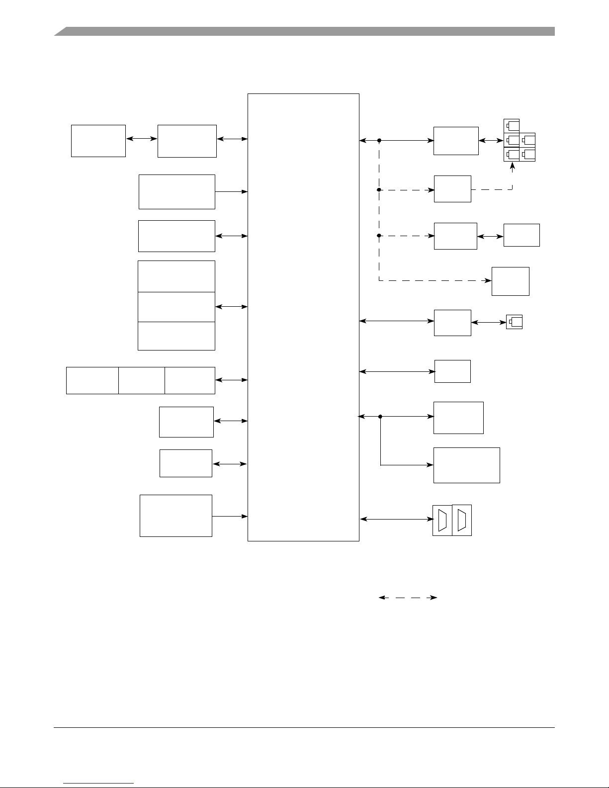
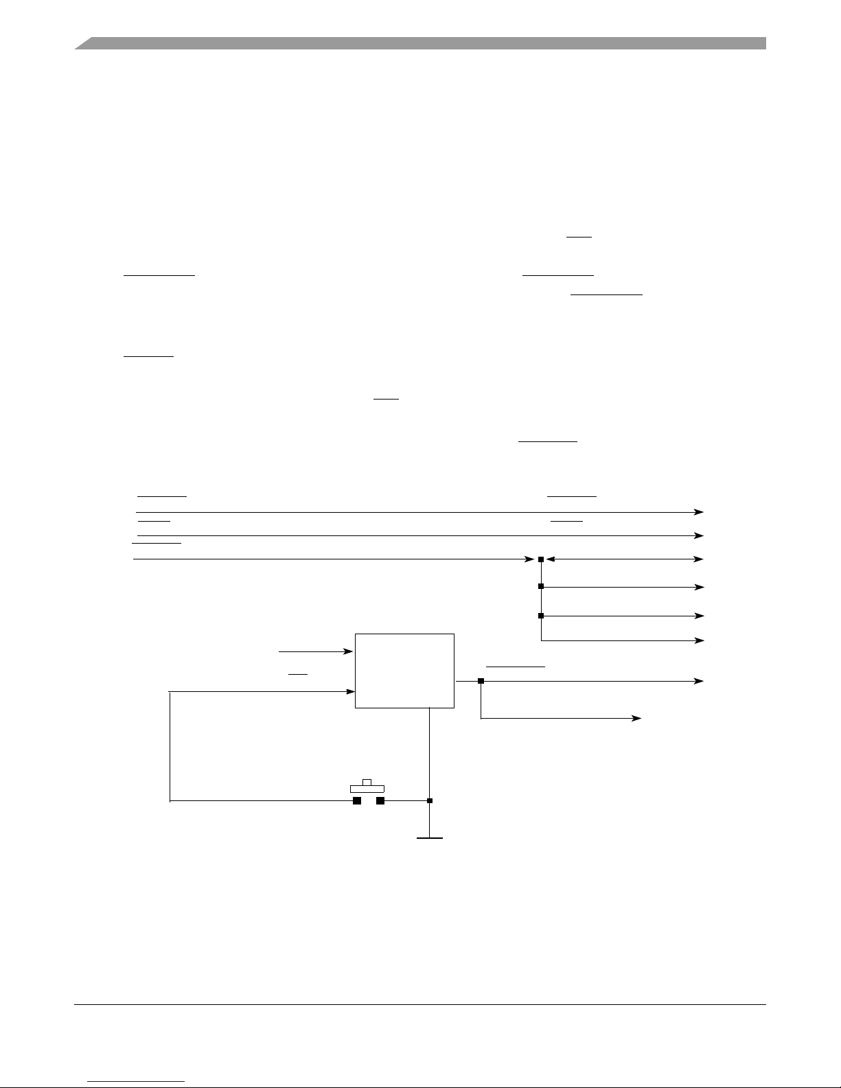
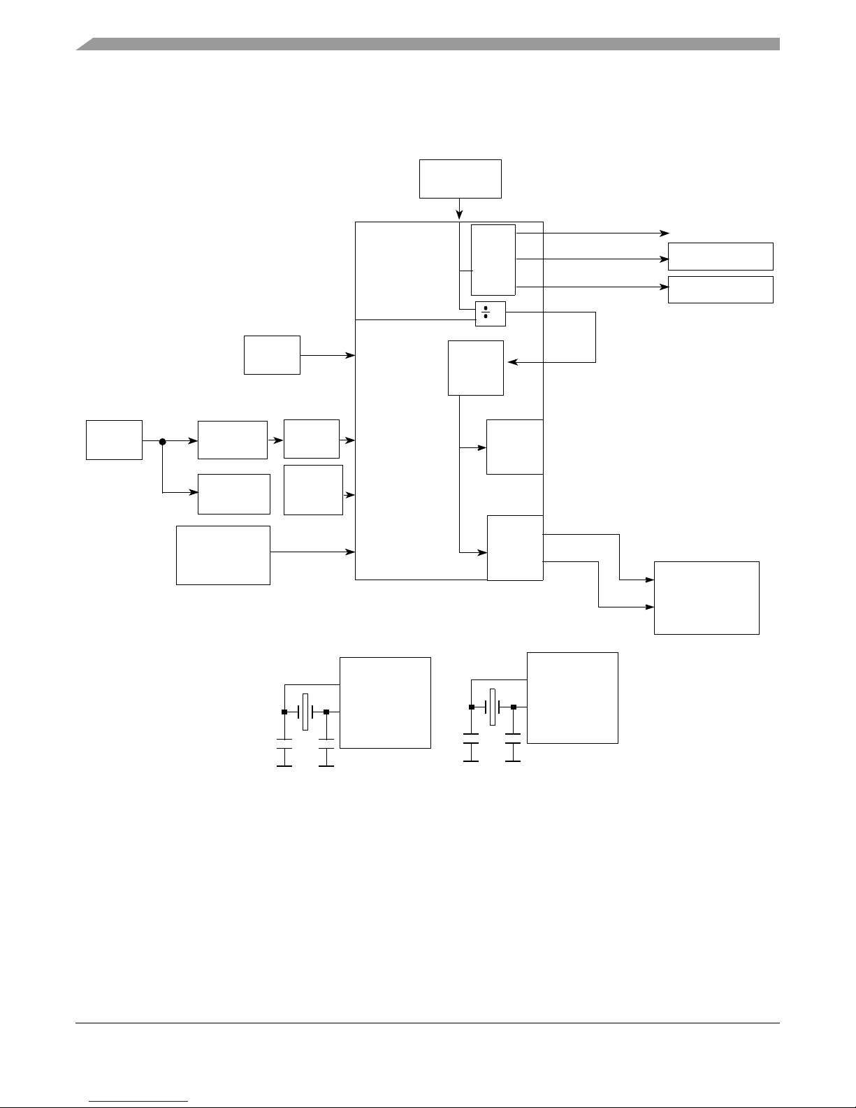
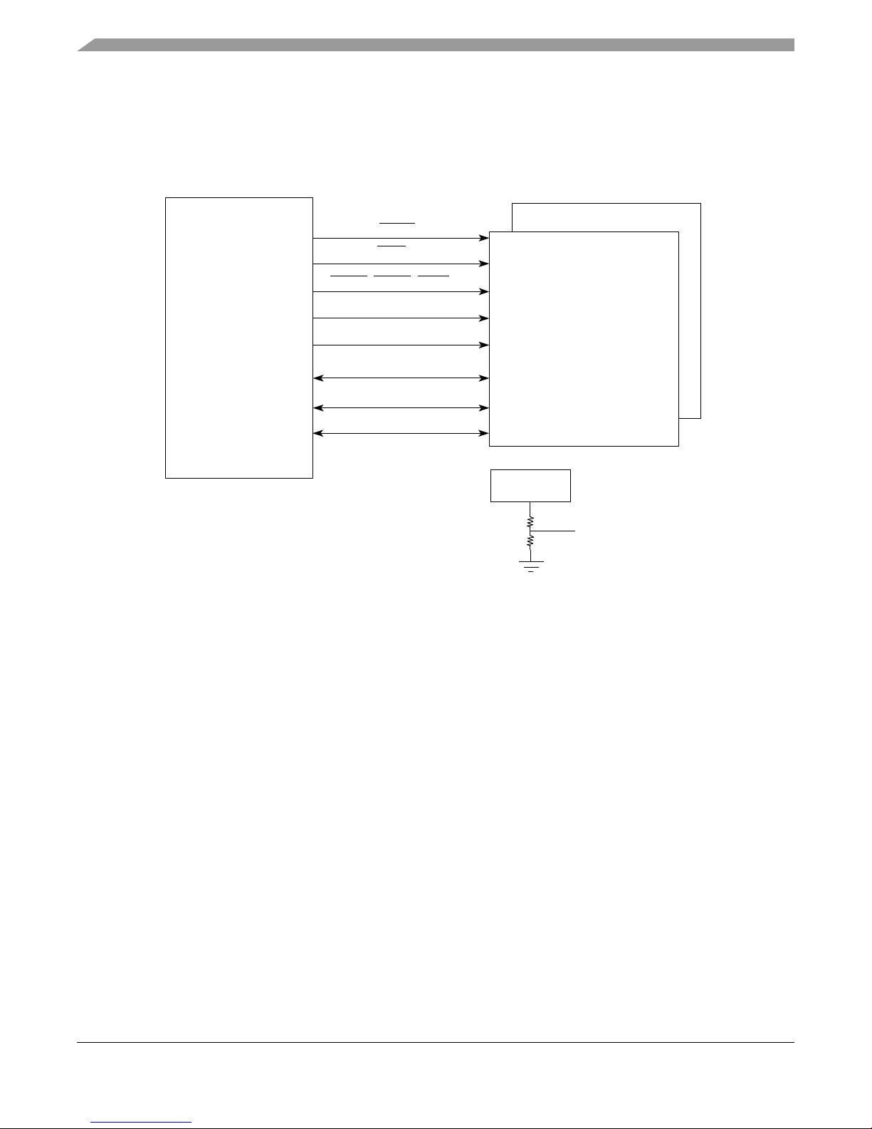
Figure 1 shows the MPC8313E RDB block diagram.
PowerQUICC™ MPC8313E Reference Design Board (RDB), Rev. 4
4 Freescale Semiconductor
Figure 1. MPC8313E RDB Block Diagram
Page 5
1.2 Specifications
Table 1 lists the specifications of the MPC8313E RDB.
Table 1. MPC8313E-RDB Specifications
Characteristics Specifications
Power requirements (without add-on card): Typical Maximum
12 V DC 0A 0 A
5.0 V DC1 mA1.5 A
Communication processor MPC8313E running at 266 MHz
MPC8313E RDB Hardware
Addressing: Total address range
Flash memory (local bus)
DDR2 SDRAM
Operating temperature 0
Storage temperature –25
Relative humidity 5% to 90% (noncondensing)
PCB dimensions:
Length
Width
Thickness
4 Gbyte (32 address lines)
8 Mbyte with one chip-select
128 Mbyte DDR2 SDRAM
o
C to 70o C (room temperature)
o
C to 85oC
6693 mil (REVA and REVB) or 7692 mil (REVC)
6693 mil
62 mil
PowerQUICC™ MPC8313E Reference Design Board (RDB), Rev. 4
Freescale Semiconductor 5
Page 6
MPC8313E RDB Hardware
1.3 Mechanical Data
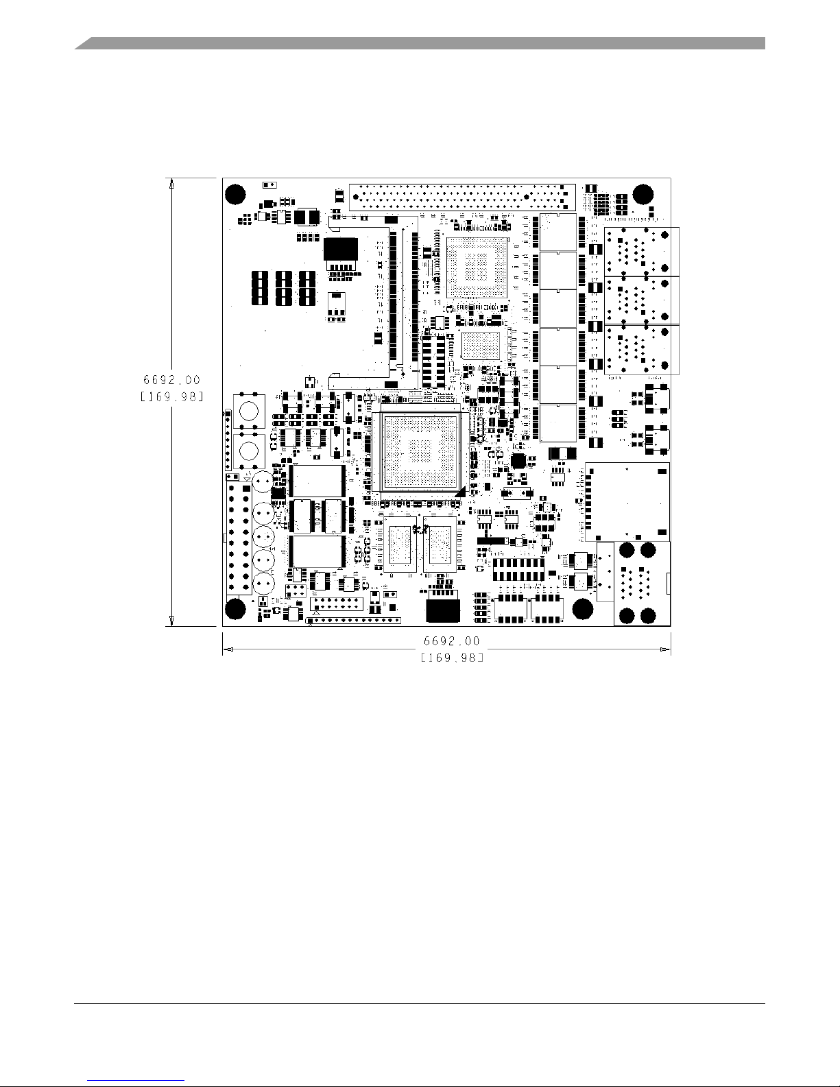
Figure 2 shows the MPC8313E RDB REVAx and REVB dimensions (in mil and [mm]). The board
measures 170 mm × 170 mm (6693 mil × 6693 mil) for integration in a mini-ITX chassis.
Figure 2. Dimensions of the MPC8313E RDB (REVAx and REVB)
PowerQUICC™ MPC8313E Reference Design Board (RDB), Rev. 4
6 Freescale Semiconductor
Page 7
Board-Level Functions
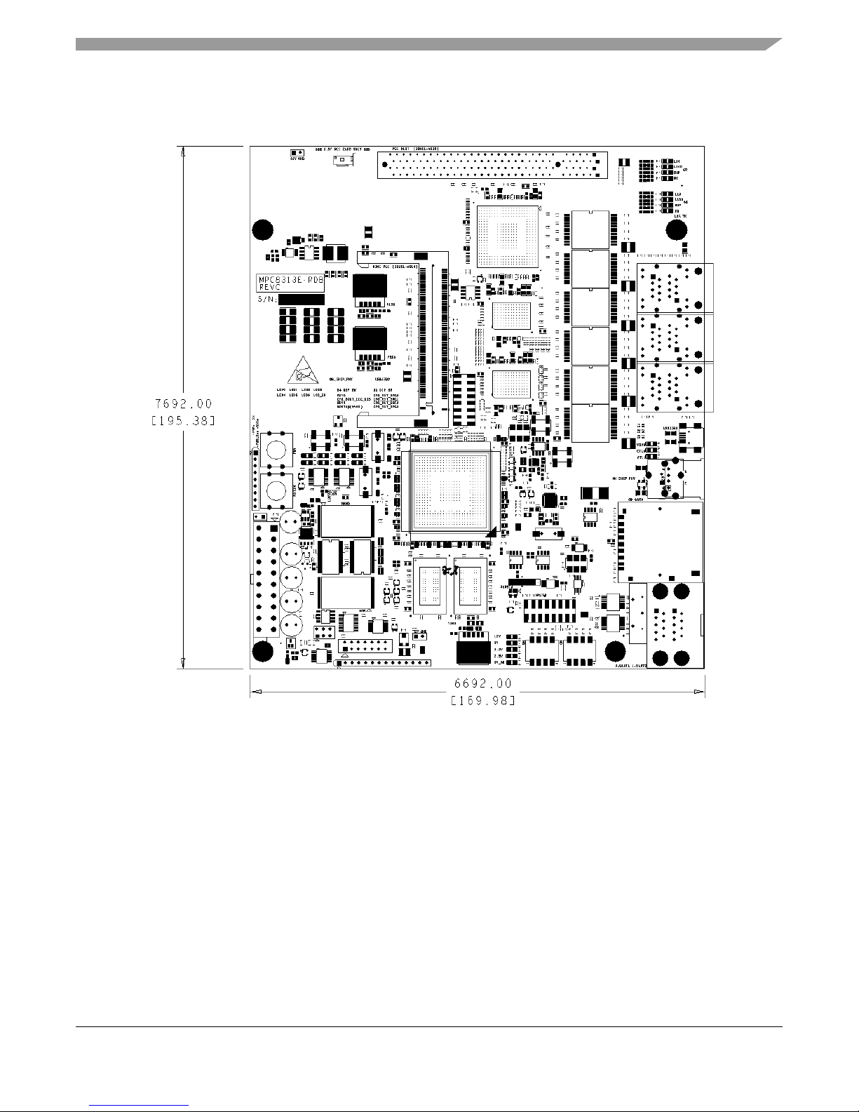
Figure 3 shows the MPC8313E RDB Rev C dimensions (in mil and [mm]). The board measures
195 mm × 170 mm (7692 mil × 6693 mil).
Figure 3. Dimensions of the MPC8313E RDB (REVC)
2 Board-Level Functions
The board-level functions are reset, external interrupts, clock distribution, DDR SDRAM controller, local
bus controller, I2C interfaces, SD memory card interface, USB interface, eTSEC1 10/100/1000 BaseT
interface, dual RS-232 ports, PCI bus, and COP/JTAG.
PowerQUICC™ MPC8313E Reference Design Board (RDB), Rev. 4
Freescale Semiconductor 7
Page 8
Board-Level Functions
MAX811
3.3 V
MR
Push Button
GND
HRESET from COP
SRESET
from COP
TRST
from COP
SRESET
to MPC8313E
TRST
to MPC8313E
PORESET
to MPC8313E
NOR FLASH
L2 Switch
MPC8313E
Reset config logic
Marvell PHY
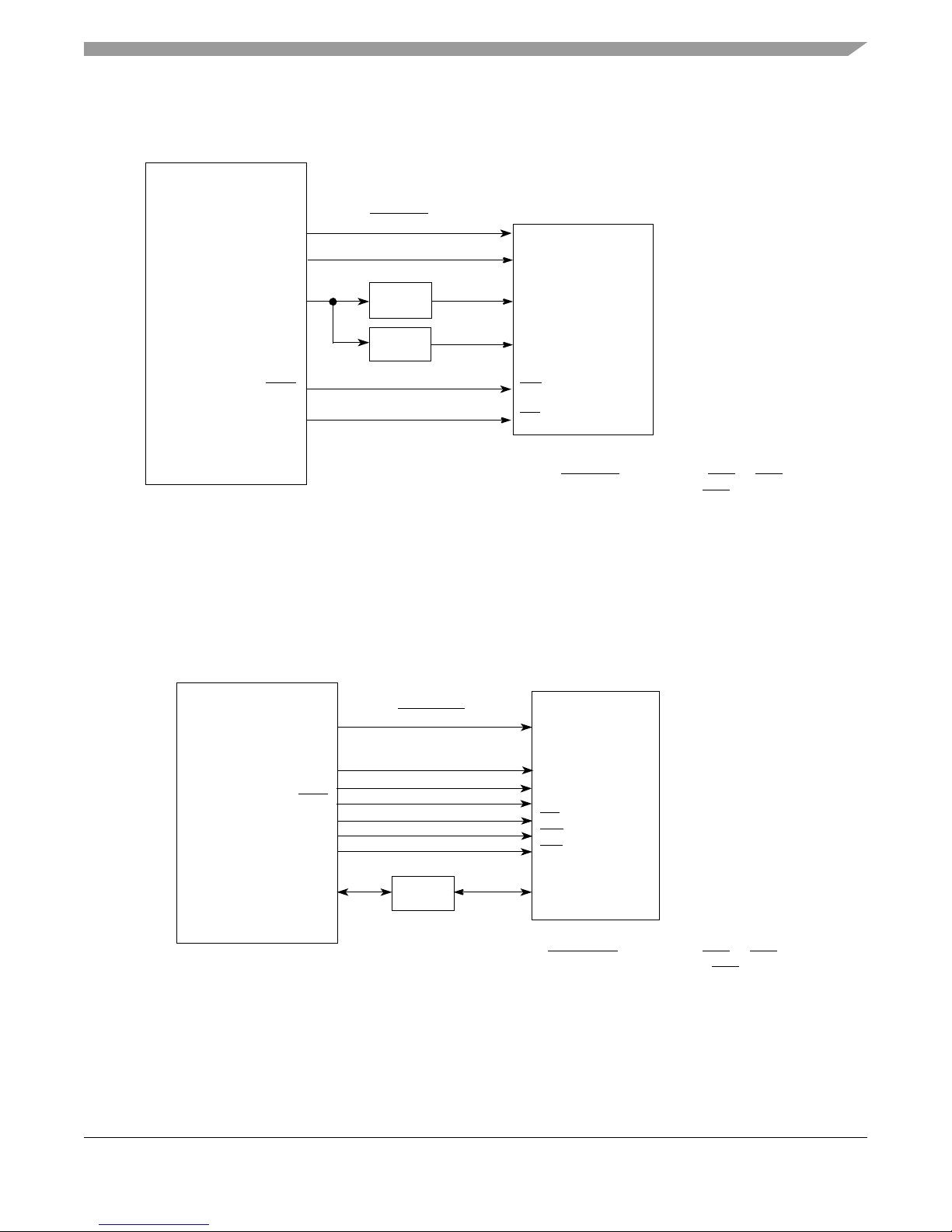
2.1 Reset and Reset Configurations
The MPC8313E RDB reset module generates a single reset to the MPC8313E and other peripherals on the
board. The reset unit provides power-on reset, hard reset, and soft reset signals in compliance with the
MPC8313E hardware specification.
Figure 4 shows the reset circuitry. Note the following:
• Hard reset is generated either by the COP/JTAG port or the MPC8313E.
• Power-on reset is generated by the Maxim MAX811 device. When MR is deasserted and 3.3 V is
ready , the MAX81 1 internal timeout guarantees a minimum reset active time of 150 ms before
PORESET is deasserted. This circuitry guarantees a 150 ms PORESET pulse width after 3.3 V
reaches the right voltage level, which meets the specification of the PORESET input of
MPC8313E.
• COP/JTAG port reset provides convenient hard-reset capability for a COP/JT AG controller. The
RESET line is available at the COP/JT AG port connector. The COP/JTAG controller can directly
generate the hard-reset signal by asserting this line low.
• Push button reset interfaces using the MR signal with debounce capability to produce a manual
master reset of the RDB.
• Soft reset is generated by the COP/JT AG port. Assertion of SRESET causes the MPC8313E to
abort all current internal and external transactions and set most registers to their default values.
PowerQUICC™ MPC8313E Reference Design Board (RDB), Rev. 4
8 Freescale Semiconductor
Figure 4. Reset Circuitry of the MPC8313E
Page 9
2.2 External Interrupts
IRQ0
IRQ2
IRQ3
IRQ4
MPC8313E
SD Card
IRQ1
PCI slot (AD15) INTA
Mini PCI (AD14) INTA and PCI slot (AD15) INTB
L2 Switch and ULPI external USB PHY (optional)
Marvell PHY, RTC (optional) and LM75 (optional)
Figure 5 shows the external interrupts to the MPC8313E.
Figure 5. MPC8313E Interrupts
The following are descriptions of the interrupt signals shown in Figure 5:
• All external interrupt signals are pulled up by 4.7 KΩ resistors.
•IRQ0 is connected to SD Card
Board-Level Functions
•IRQ1 is connected to PCI slot INTA.
•IRQ2 is connected to and shared by the PCI slot’s INTB and the mini PCI slot INTA.
•IRQ3 is connected to the L2 switch as well as to an external USB PHY (by an optional resistor).
•IRQ4 is connected to the Marvell GBE PHY as well as to RTC and LM75 (by an optional resistors).
Freescale Semiconductor 9
PowerQUICC™ MPC8313E Reference Design Board (RDB), Rev. 4
Page 10
Board-Level Functions
MPC8313E
LCLKx (NC)
local bus
PLL
DDR
PLL
PCI
DIV
66.666 MHz
OSC
CLKIN
33/66 MHz
33/66 MHz
Mini PCI Slot
PCI Slot
OCCR
2
PCI_SYNC_OUT
PCI_SYNC_IN
System
PLL
M66EN
33/66 MHz
CFG_CLKIN_DIV
NC
48 MHz
OSC
25 MHz
OSC
USB
CLKIN
L2 Switch
GBE PHY
GTX_CLK125
SD_REF_CLK
50 MHz OSC/
50 MHz VCXO
IEEE1588
TMR CLK
0
1
2
ULPI USB
GND GND
24 MHz
Crystal
PHY
Real-Time
GND GND
32.768 KHz
Crystal
Clock
DDR2 SDRAM
CLK
MCK
MCK#
133 MHz
PLL
125 MHz
LVD S
OSC
125MHz
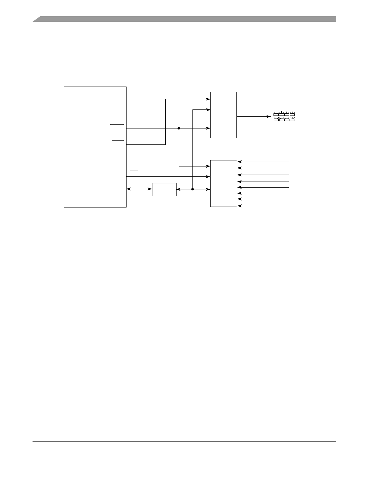
2.3 Clock Distribution
Figure 6 and Table 2 show the clock distribution on the MPC8313E RDB.
Figure 6. MPC8313E-RDB Clock Scheme
PowerQUICC™ MPC8313E Reference Design Board (RDB), Rev. 4
10 Freescale Semiconductor
Page 11
Board-Level Functions
Table 2. Clock Distribution
Clock Frequency Module Generated by Description
66.666 MHz MPC8313E CLKIN 66.666 MHz oscillator The MPC8313E uses CLKIN to generate the
PCI_SYNC_OUT clock signal, which is fed back
on the board through the PCI_SYNC_IN signal
to the internal system PLL. From the power-on
reset configuration, the CSB clock is generated
by the internal PLL and is fed to the e300 core
PLL for generating the e300 core clock. The
CFG_CLKIN_DIV
whether CLKIN or CLKIN/2 is driven on the
PCI_SYNC_OUT signal. The CFG_CLKIN_DIV
is tied to the M66EN input pin.
133 MHz DDR2 SDRAM MPC8313E The DDR memory controller is configured to use
the 2:1 mode CSB to DDR for the DDR interface
(DDR266). The local bus clock uses 1:1 local to
CSB clock, which is configured by hard reset
configuration or SPMR register.
configuration input selects
33/66 MHz PCI 32-bit slot and MiniPCI
slot
25 MHz L2 Switch and GBE PHY 25 MHz oscillator The 25 MHz oscillator provides the clock for the
125 MHz eTSEC clock GBE PHY with PLL
48 MHz USB clock 48 MHz oscillator 48 MHz is provided for on-chip USB PHY of
50 MHz IEEE1588 Clock (TMR_CLK) 50 MHz oscillator/50
24 MHz ULPI external USB PHY 24 MHz crystal 24 MHz crystal is used by the ULPI external
32.768 KHz Real-time clock 32.768 KHz crystal 32.768 KHz crystal is used by the real-time clock
MPC8313E The PCI module uses the PCI_SYNC_IN as its
clock source. The trace length of the
PCI_SYNC_IN to PCI_SYNC_OUT signal is
matched with all PCI clocks on the RDB.
L2 switch and the GBE PHY
The GTX_CLK125 and SERDES (SGMII) clocks
(REVC), or
125 MHz oscillators
(REVB), or
GBE PHY (REVAx)
MHz VCXO
are provided by external oscillators (or by GBE
PHY in REVAx and REVC boards).
MPC8313E
50 MHz is used by the IEEE 1588 module. It can
be an ordinary oscillator or VCXO controlled by
SPI DAC.
USB PHY
2.4 DDR2 SDRAM Controller
The MPC8313E processor uses DDR2 SDRAM as the system memory. The DDR2 interface uses the
SSTL2 driver/receiver and 1.8 V power. A Vref 1.8 V/2 is needed for all SSTL2 receivers in the DDR2
interface. For details on DDR2 timing design and termination, refer to the Freescale application note
entitled “Hardware and Layout Design Considerations for DDR Memory Interfaces” (AN2582). Signal
integrity test results show this design does not require terminating resistors (series resistor (R
termination resistor (R
)) for the discrete DDR2 devices used. DDR2 supports on-die termination; the
T
DDR2 chips and MPC8313E are connected directly. The interface is 1.8 V provided by an on-board
PowerQUICC™ MPC8313E Reference Design Board (RDB), Rev. 4
Freescale Semiconductor 11
) and
S
Page 12
Board-Level Functions
DDR2 Device (512 Mbit, 16-Bit)
MPC8313E
DDR2
Controller
DDR2 Device (512 Mbit, 16-Bit)
MCS0
MCK, MCK, MCKE
MRAS
, MCAS, MWE
MDM[0:3], MDQS[0:3]
A[0:14], BA[0:2]
MDQ[0:31]
ODT
VREF
1.8 V Reg
VREF
voltage regulator. VREF, which is half the interface voltage, or 0.9 V, is provided by a voltage divider of
1.8 V for voltage tracking and low cost. The MPC8313E provides a pair of clock pins, which are connected
and shared by the two DDR2 devices.
Figure 7 shows the DDR2 SDRAM controller connection.
2.5 Local Bus Controller
The MPC8313E local bus controller has a 26-bit LAD[0–15] and LA[16–25] address that consists of
16-bit data multiplex bus and control signals. The local bus speed is up to 133 MHz. T o interface with the
standard memory device, an address latch must provide the address signals. The LALE is used as the
latching signal. To reduce loading of the high speed local bus interface, a data buffer for all low-speed
devices is attached to the memory controller. The followings modules are connected to the local bus:
2.5.1 NOR Flash Memory
Through the general-purpose chip-select machine (GPCM), the MPC8313E RDB provides 8 Mbyte of
flash memory using a chip-select signal. The flash memory is used with the 16-bit port size. Figure 8
Figure 7. DDR2 SDRAM Connection
• 8 Mbyte NOR flash memory
• 32 Mbyte NAND flash memory
• LED/status buffer s
PowerQUICC™ MPC8313E Reference Design Board (RDB), Rev. 4
12 Freescale Semiconductor
Page 13
Board-Level Functions
MPC8313E
eLBC
Controller
NOR
Flash 16-Bit
NOR_CS
*NOTE: NOR_CS
can be either CS0 or CS1
by DIP switch option, default is CS0
Latch
Buffer
LA[24:16]
A[0:8]
A[9:21]
LBA[15:3]
LAD[15:0]
DQ[0:15]
LBD[15:0]
WE
OE
WE0
GPL2
MPC8313E
eLBC
Controller
NAND
Flash 8-Bit
NAND_CS
*NOTE: NAND_CS
can be either CS0 or CS1
by DIP switch option; the default is CS1
CLE
ALE
WE
RE
R/B
WP
GPL0
GPL1
WE0
GPL2
GPL4
GPL3
LAD[0:7] IO[7:0]
*Buffer
LBD0-7
shows the hardware connections for the flash memory . The starting address for the 8 M byte flash memory
is 0xFE00_0000 to 0xFE7F_FFFF.
2.5.2 NAND Flash Memory
The MPC8313E has native support for NAND Flash memory through its NAND Flash control machine
(FCM). The MPC8313E RDB implements an 8-bit NAND Flash with 32 Mbyte in size. Figure 9 shows
the NAND Flash connection.
Freescale Semiconductor 13
Figure 8. NOR Flash Connection
PowerQUICC™ MPC8313E Reference Design Board (RDB), Rev. 4
Figure 9. NAND Flash Connection
Page 14
Board-Level Functions
MPC8313E
eLBC
Controller
WE0
GPL2
LAD[0:7]
Buffer
LCS3
LCX373
LCX245
8x LEDs
Write Buffer
Read Buffer
SD_INSERT
SD_PROTECT
RSVD0
BOOT0
RSVD1
M66EN
REV0
REV1
LBD[0:7]
OE
2.5.3 LED/Status Buffers
The MPC8313E RDB has an 8-bit read/write buffer . The read buffer returns information on M66EN, board
revision, boot device (NOR or NAND), and SD card status. The write buffer controls eight LEDs on the
board for status or debug indication. Figure 10 shows the hardware connection of the buffers.
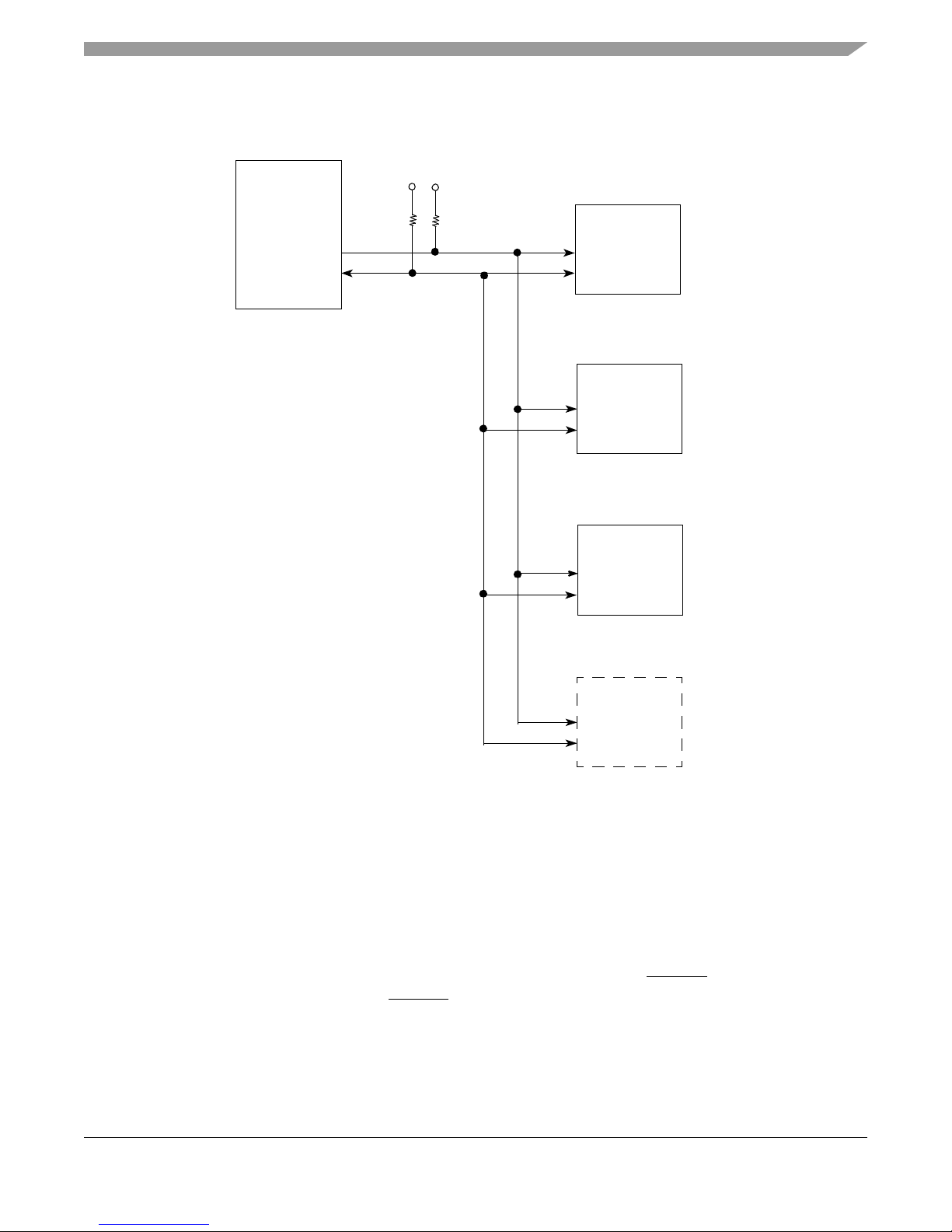
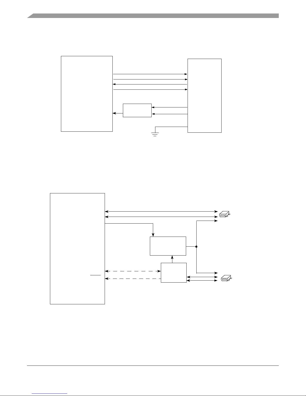
2.6 I2C Interfaces
The MPC8313E has two I2C interfaces. On the MPC8313E RDB, I2C1 is used as master mode. It is
connected to the following three devices as shown in Figure 11.
It may also be connected to the DAC AD5301 at addres s 0x0C, whose optional nature is represented in
Figure 11 by the dashed line.
The connection of the I
the reset configuration word of the MPC8313E, as well as to store the configuration registers’ values and
user program if the MPC8313E boot sequencer is enabled. By default, the EEPROM is not used and the
hard reset configuration words are loaded from local bus flash memory. For details about how to program
Figure 10. LED/Status Buffers
• Serial EEPROM M24256 at address 0x50.
• Real-time clock DS1339U at address 0x68.
• Thermal sensor LM75 at address 0x48.
2
C bus is shown in Figure 11. The M24256 serial EEPROM can be used to store
14 Freescale Semiconductor
PowerQUICC™ MPC8313E Reference Design Board (RDB), Rev. 4
Page 15
Board-Level Functions
I2C1-SCL
I2C EEROM
M24256
MPC8313E
SCL
SDA
I2C1-SDA
I
2
C Address = 0x50
I2C RTC
DS1339U
SCL
SDA
I
2
C Address = 0x68
I2C Sensor
LM75
SCL
SDA
I
2
C Address = 0x48
3.3 V
I2C DAC (Optional)
AD5301
SCL
SDA
I
2
C Address = 0x0C
the reset configuration word value i n I2C EEPROM and the boot se quencer mode, refer to the MPC8313E
reference manual.
Figure 11. I2C Connection
2.7 SD Memory Card Interface
An SD memory card interface connects directly to the SPI bus of the MPC8313E. SD data mode and SDIO
mode are not supported. The SPI mode is the only SD operating mode supported by this connection. Hot
insertion and removal is not supported. See Figure 12 for the hardware connection.
For REVB boards, the SD card chip select signal is changed from GPIO31(SPISEL) to GPIO13(LA8)
because when using SPI as master mode, SPISEL
device select signal). In this case, another GPIO pin should be used. GPIO13 is implemented on this board
as an example.
cannot be set as GPIO (which is supposed to be used for
PowerQUICC™ MPC8313E Reference Design Board (RDB), Rev. 4
Freescale Semiconductor 15
Page 16
Board-Level Functions
MPC8313E
CS
DIN
DOUT
SCLK
INSERT
CONTACT
PROTECT
SD_CS
SPIMOSI
SPIMISO
SPICLK
SD_INSERT
SD_CONTACT
SD_PROTECT
LA8 (GPIO13)
SPIMOSI
SPIMISO
SPICLK
SD Memory Card Socket
Status Read
Buffer
Local Bus
MPC8313E
USB-DP
USB-DM
USB mini-AB
On-Chip
USB PHY
ULPI external
USB PHY Interface
USB3300
USB PHY
USB VBUS
Power Supply
USB mini-AB
USB-VBUS
Control
Control
**ULPI
IRQ3
**NOTE: Because ULPI is multiplexed with eTSEC1 RGMII, by default
on-chip PHY is used. A change of resistor option is needed to use
the external USB PHY interface.
OR
Power down before inserting or removing the SD memory card.
2.8 USB Interface
CAUTION
Figure 12. SD Memory Card Connection
MPC8313E supports a USB 2.0 high speed host/device i nterface through its on-chip USB PHY or external
ULPI USB PHY. The MPC8313E R DB s upports both options. By default, the on- chip USB PHY is used.
Figure 13 shows the USB connections.
Figure 13. USB Connections
16 Freescale Semiconductor
PowerQUICC™ MPC8313E Reference Design Board (RDB), Rev. 4
Page 17

Board-Level Functions
VSC7385
MPC8313E
RGMII
eTSEC1
Local Bus
LCS2#, GPCM 8bit data
RJ-45 ports
L2 switch
MPC8313E
RGMII
eTSEC2
88E1111
GBE PHY
SGMII
RJ-45 Port
NOTE: By default, RGMII is used and SGMII is optional
MDC, MDIO
MDIO PHY
Address = 4
2.9 eTSEC1 10/100/1000 BaseT Interface
eTESC1 is set to operate in RGMII mode. It connects to a VSC7385 5-port L2 switch, as shown in
Figure 14.
Figure 14. RGMII Interface Connection for L2 Switch
2.10 eTSEC2 10/100/1000 BaseT Interface
eTESC2 can be set to operate in RGMII mode (default) or SGMII mode. Figure 15 shows the hardware
connection for eTSEC.
Figure 15. eTSEC2 Connection
Freescale Semiconductor 17
PowerQUICC™ MPC8313E Reference Design Board (RDB), Rev. 4
Page 18

Board-Level Functions
MPC8313E
UART1
RXD
RTS
TXD
CTS
UART2
RXD
RTS
TXD
CTS
MAX3232
TXD
RXD
CTS
RX
TX
TX
DO
DI
DI
RTS
Female DB-9
RS-232
Serial
Por t
RX
DO
3
7
8
2
MAX3232
TXD
RXD
CTS
RX
TX
TX
DO
DI
DI
RTS
Female DB-9
RS-232
Serial
Por t
RX
DO
3
7
8
2
MPC8313E
32Bit PCI
PCI-AD[0:31]
PCI-CBE[0:3]
PCI-REQ0
PCI-GNT0
PCI-CTRL
32Bit 3.3 V
PCI Slot
32-Bit 3.3 V
MiniPCI Slot
PCI-REQ1
PCI-G NT1
[AD14]
[AD15]
2.11 Dual RS-232 Ports
Dual RS-232 ports are supported on the RDB. Figure 16 illustrates the serial port connection using a
MAX3232 3.3 V RS-232 driver to interface with a 9-pin D type female connector . Thi s serial connection
runs at up to 115.2 Kbps.
Figure 16. RS-232 Debug Ports Connection
2.12 PCI Bus
The 32-bit PCI interface connects to a 32-bit 3.3 V PCI slot and a miniPCI slot (see Figure 17).
18 Freescale Semiconductor
PowerQUICC™ MPC8313E Reference Design Board (RDB), Rev. 4
Figure 17. PCI Bus Connection
Page 19

Connectors, Jumpers, Switches, and LEDs
PC
MPC8313E RDB
P1
USB
Emulator
USB Port
COP Port
TDI
Pull-up
TCK
TMS
SRESET
HRESET
CKSTP_OUT
GND
TRST
Pull-up
CKSTP_IN
NC
NC
NC
GND
1
TDO
2.13 COP/JTAG Port
The common on-chip processor (COP) is part of the MPC8313E JTAG module and is implemented as a
set of additional ins tructions and logi c. This por t can connect to a dedicated emulator for extensive system
debugging. Several third-party emulators in the market can connect to the host computer through the
Ethernet port, USB port, parallel port, RS-232, and so on. A typical setup using a USB port emulator is
shown in Figure 18.
Figure 18. Connecting MPC8313E-RDB to a USB Emulator
The 16-pin generic header connector carries the COP/JTAG signals and the additional signals for system
debugging. The pinout of this connector is shown in Figure 19.
Figure 19. MPC8313E RDB COP Connector
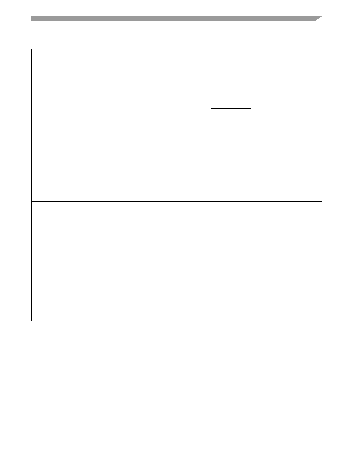
3 Connectors, Jumpers, Switches, and LEDs
Table 3 summarizes the connectors, jumpers, switches, and LEDs on the MPC8313E RDB and provides
the number of the section/page on which each is discussed. The rest of this section discusses each of these
in the order of its appearance in the table.
Table 3. Connectors, Jumpers, Switches, and LEDs
Reference Description Section/Page
Freescale Semiconductor 19
P1 14-pin COP/JTAG connector 3.1/Page 21
PowerQUICC™ MPC8313E Reference Design Board (RDB), Rev. 4
Connectors
Page 20

Connectors, Jumpers, Switches, and LEDs
Table 3. Connectors, Jumpers, Switches, and LEDs (continued)
Reference Description Section/Page
P2 3.3 V PCI Slot [IDSEL - AD15] 3.2/Page 21
P3 MiniPCI Slot [IDSEL - AD14] 3.3/Page 22
P4 USB mini-AB Connector (on-chip PHY) 3.4/Page 22
P5 RJ-45 LAN connectors Enet4 (top), Enet5 (bottom). See Figure 23 3.5/Page 23
P6 RJ-45 LAN connectors Enet2 (top), Enet3 (bottom). See Figure 23
P7 RJ-45 LAN connectors Enet0 (top), Enet1 (bottom). See Figure 23
P8 USB mini-AB Connector (external ULPI USB PHY) 3.4/Page 22
P9 ATX type power supply connector. The board can be powered by an ATX power supply or
—
the power supply bundled with the mini-ITX case.
P10 IEEE 1588 connector (Optional) 3.9/Page 25
P11 Dual UART connector. UART1 (top), UART2 (bottom) 3.6/Page 24
U44 SD memory card socket 3.7/Page 24
BT1 RTC battery holder, CR2032 type. The real-time clock on the RDB requires a battery when
—
the board is powered off. When placing or replacing the battery, take care to ensure that the
polarity is correct.
J20 Connector for chassis connection (power on, power LED, reset) —
J21 LCD connector 3.8/Page 24
J22 LCD connector
J23 LCD backlight connector. A 2-pin header (J23) is provided for LCD backlight power. Pin1 is
—
5 V and pin 2 is GND.
J24 MCU programming connector. J24 is used for MCU programming on the RDB. It is reserved. —
Jumpers
J19 Open (Default)—Power ON controlled by switch; Close—Power is always ON —
Switches
S1 System reset button. Resets the MPC8313E RDB. (PORESET
button reset switch on the RDB to cause a power-on reset (PORESET
). Press once on the push
) to the board.
—
S2 Power ON button. Press once to power ON/OFF. —
S3 DIP switch. Selects the reset configuration source (RST_CFG_SRC) for the MPC8313E. 3.10/Page 26
S4 DIP switch. Board revision indicator and boot device selector. 3.11/Page 26
D6 Enet5 Link 10 —
D7 Enet5 Link 100 —
D8 Enet5 Duplex —
D9 Enet5 RX —
D12 USB VBUS —
D10 On-chip USB PHY CTL0 —
PowerQUICC™ MPC8313E Reference Design Board (RDB), Rev. 4
20 Freescale Semiconductor
LEDs
Page 21

Connectors, Jumpers, Switches, and LEDs
Table 3. Connectors, Jumpers, Switches, and LEDs (continued)
Reference Description Section/Page
D11 On-chip USB PHY CTL1 —
D16 12-V Indicator —
D15 5-V Indicator —
D14 3.3-V Indicator —
D17 2.5-V Indicator —
D13 5-V standby indicator —
D3 Programmable LED0 (Red) 3.12/Page 27
D5 Programmable LED1 (Yellow)
D2 Programmable LED2 (Green)
D1 Programmable LED3 (Green)
D22 Programmable LED4 (Green)
D21 Programmable LED5 (Green)
D20 Programmable LED6 (Green)
D4 Programmable LED7/LCD_EN (Green)
3.1 COP Connector (P1)
The COP connector allows the user to connect a COP/JTAG-based debugger to the MPC8313E RDB for
debugging. Table 4 lists the pin assignments of the COP connector.
Table 4. COP Connector Pin Assignments
Pin Signal Pin Signal
1 TDO 2 GND
3 TDI 4 TRST
5QREQ 6 VDD_SENSE
7 TCK 8 CKSTP_IN
9TMS 10 NC
11 SRESET
13 HRESET
15 CKSTP_OUT 16 GND
12 NC
14 NC
3.2 PCI Slot (P2)
The MPC8313E RDB has one 32-bit 3.3-V PCI expansion slot (P2) for an expansion card. The slot
connects AD15 for its device select signal. Only the 3.3-V PCI card is supported. Turn OFF power during
PowerQUICC™ MPC8313E Reference Design Board (RDB), Rev. 4
Freescale Semiconductor 21
Page 22

Connectors, Jumpers, Switches, and LEDs
PCI Slot
5 V Key
Match
3.3 V Key
Here
Front Panel
ATX p owe r
Connector
M
i
n
i
P
C
I
C
a
r
d
1
.
I
n
s
e
r
t
2. Press down
insertion and removal of the PCI card. As Figure 20 shows, 3.3-V PCI cards can be identified by the key
position on the PCI card.
Figure 20. 3.3 V Key on a Typical 3.3 V PCI Card
3.3 MiniPCI Connector (P3)
There is a MiniPCI connector (P3) on the RDB. The slot connects to AD14 for its device select signal.
Figure 21 shows how to install a MiniPCI card.
3.4 USB Connectors (P4, P8)
There are two USB connectors on the MPC8313E RDB . One connects to the on-chip PHY of the
MPC8313E, and the other connects to the external ULPI USB PHY. Either can be enabled at a time. The
PowerQUICC™ MPC8313E Reference Design Board (RDB), Rev. 4
22 Freescale Semiconductor
Figure 21. Installation of MiniPCI Card
Page 23

Connectors, Jumpers, Switches, and LEDs
USB LEDs:
CTL1
CTL0
VBUS
for external
ULPI USB PHY
for on-chip
PHY
G0
G1
G2
G3
G4
G5
USB mini-AB
USB Type A
RX
Duplex
Link100
Link10
G5 LEDsLink1000
TX
A
B
A
B
A
B
A
B
A
B
A: Link/Activity 1000
B: Link/Activity 10/100
G0-G4 LEDs:
selection between the two requires modification of micro-jumpers/resistor options as discussed later. By
default, the on-chip PHY USB is used. Figure 22 shows the USB connectors in front panel.
Figure 22. USB Connectors
3.5 Ethernet Connectors (P5, P6, P7)
The MPC8313E RDB has six Ethernet ports (RJ-45). The first five ports (G0–G4) are supported by
eTSEC1 (L2 switch), and the last port (G5) is supported by eTSEC2 (GBE PHY). Figure 23 shows the
G0–G5 mapping viewing from the front panel.
Freescale Semiconductor 23
PowerQUICC™ MPC8313E Reference Design Board (RDB), Rev. 4
Figure 23. Ethernet Connectors
Page 24

Connectors, Jumpers, Switches, and LEDs
UART1
UART2
SD Memory
1GB
Card
3.6 RS-232 UART Connector (P11)
Serial interfaces are available at connector P11. It is a double deck RS-232 female connector. The upper
port is UART1 and the lower port is UART2. By default, UAR T 1 is used. Figure 24 shows the RS-232
UART connector front view.
.
Figure 24. RS-232 UART Connectors
3.7 SD Memory Card Socket (U44)
An SD card socket (U44) for SD memory card installation is located next to the UART connector of the
board. Figure 25 shows how to install a compact flash card.
3.8 LCD Connectors (J21, J22)
T wo headers (J21, J22) are provided for LCD connections. They use the MPC8313E GPIO interface. Both
headers carry the same set of GPIO signal pins, but they are different physically. J21 is single row of
1 × 14, and J22 is double row of 2 × 7. Table 5 shows the mapping.
PowerQUICC™ MPC8313E Reference Design Board (RDB), Rev. 4
24 Freescale Semiconductor
Figure 25. Installation of SD Card
Table 5. LCD Connector Pin Assignment
Pin Number Description
1GND
25V
3 5 V to –5 V variable
4GPIO2
5GPIO3
6GPIO1
Page 25

Connectors, Jumpers, Switches, and LEDs
TSEC_TMR_PP1
TSEC_TMR_PP2
TSEC_TMR_PP3
GND
GND
GND
TSEC_TMR_GCLK
TSEC_TMR_ALARM1
TSEC_TMR_ALARM2
TSEC_TMR_TRIG1
TSEC_TMR_TRIG2
TSEC_TMR_TRIG2
GND
TSEC_TMR_CLK
1
3.3 V
by TSEC1 PHY)
3.3 V
(Optional if not used
by TSEC1 PHY)
(Optional if not used
Table 5. LCD Connector Pin Assignment (continued)
Pin Number Description
7 Pull-down
8 Pull-down
9 Pull-down
10 Pull-down
11 GPIO7
12 GPIO6
13 GPIO5
14 GPIO4
3.9 IEEE 1588 Connector (Optional)
A header (P10) is provided for IEEE 1588 signals connection. It is double r ow of 2 × 8 header connector.
The pinout of this connector is shown in Figure 26.
Figure 26. IEEE 1588 Connector (Optional)
Freescale Semiconductor 25
PowerQUICC™ MPC8313E Reference Design Board (RDB), Rev. 4
Page 26

Connectors, Jumpers, Switches, and LEDs
1
2
3
4
ON
CFG_RST_SRC0
0
1
CFG_RST_SRC1
CFG_RST_SRC2
CFG_RST_SRC3
1
2
3
4
ON
0
1
RSVD
REV1
BOOT1
(NAND)
CFG_BOOT_ECC_DIS
3.10 DIP Switch S3
DIP switch S3 selects the reset configuration source (RST_CFG_SRC) for the MPC8313E. Figure 27
shows the factory default configuration of S3.
Figure 27. DIP Switch S3
Check the MPC8313E reference manual for the meaning of the CFG_RST_SRC combination. By default,
the DIP switch is set to all ON, meaning CFG_RST_SRC[0..3] = 0000. In this case, the hardware reset
configuration is loaded from local bus NOR flash memory.
3.11 DIP Switch S4
DIP switch S4 on the RDB is shown in Figure 28, with the factory default configuration.
RSVD is reserved. When software options are implemented, their values can be read from a buffer on the
board. CFG_BOOT_ECC_DIS switch is OFF by default to disable booting with ECC by driving HIGH to
PowerQUICC™ MPC8313E Reference Design Board (RDB), Rev. 4
26 Freescale Semiconductor
Figure 28. DIP Switch S4
Page 27

Micro-Jumper/Resist or Options for eTSEC1
LED0 LED1
LED2
(Red) (Yellow)
(Green)
LED3
(Green)
LED4
(Green)
LED5
(Green)
LED6
(Green)
LED7/LCD_EN
(Green)
the signal LB_POR_CFG_BOOT_ECC_DIS (TSEC1_MDC) during power on reset (REVB and REVC
only . REVAx is a reserved switch (RSVD0)). REV1 represents bit 1 of the revision number. T ogether with
REV0 (implemented by resistor option; the default is 0), REV[0..1] shows the revision number, which is
01 by default. The values can be read from a buffer on the RDB. BOOT1 selects the boot device on the
RDB. By default, BOOT1 is set, so chip-select 0 (CS0) is connected to the NOR Flash. CS1 is connected
to the NAND Flash memory. If BOOT1 is cleared, CS0 is connected to NAND Flash memory, and CS1 is
connected to NOR Flash memory.
3.12 RDB Programmable LEDs
Eight programmable LEDs give status indication and debug information. Figure 29 shows the diagram.
Figure 29. Programmable LEDs
An 8-bit write register on the RDB turns the LEDs on and off. The LEDs are arranged so that the most
significant bit represents LED0 and least significant bit represents LED7; that is, LED[0..7]. A write of
0x00 turns on all LEDs, and 0xFF turns off all LEDs.
4 Micro-Jumper/Resistor Options for eTSEC1
The eTSEC1 RGMII, ULPI USB, and IEEE 1588 signals are multiplexed on the MPC8313E. The
MPC8313E RDB supports switching among the three interfaces using micro-jumpers (REVA boards) or
resistor options (REVA1 or later boards).
NOTE
For IEEE 1588 support, use the same setting as for the eTS EC1 RGMII. In
this case, a 50 MHz clock would be provided for the IEEE 1588 TMR_CLK
pin.
PowerQUICC™ MPC8313E Reference Design Board (RDB), Rev. 4
Freescale Semiconductor 27
Page 28

Micro-Jumper/Resistor Options for eTSEC1
4.1 For REVA Boards
Figure 30 shows the micro-jumper locations.
Figure 30. REVA Micro-jumper Locations
By default the REVA boards are shipped with the following settings:
Setup 1:
• eTSEC1, RGMII
• eTSEC2, RGMII
The corresponding micro-jumper settings are shown in Table 6.
Table 6. Default Micro-jumper Settings for REVA
Jumper Setting Jumper Setting Jumper Setting Jumper Setting
J13 1-2 J7 1-2 J5 open J18 2-3
J12 1-2 J9 1-2 J1 open
J16 1-2 J6 1-2 J2 open
J15 1-2 J8 1-2
J17 1-2 J3 1-2
J14 1-2 J4 1-2
J11 open
J10 1-2
PowerQUICC™ MPC8313E Reference Design Board (RDB), Rev. 4
28 Freescale Semiconductor
Page 29

Micro-Jumper/Resist or Options for eTSEC1
There are alternative sett i ngs f or RE VA boar ds:
Setup 2:
• eTSEC1, USB DR with external ULPI USB PHY (USB3300)
• eTSEC2, SGMII (remove R87, C275; connect 125 MHz clock from R181 to SGMII SCLK)
The corresponding micro-jumper settings are shown in Table 7.
Table 7. Alternative Micro-jumper Settings for REVA (Setup 2)
Jumper Setting Jumper Setting Jumper Setting Jumper Setting
J13 open J7 2-3 J5 2-3 J18 1-2
J12 open J9 2-3 J1 2-3
J16 open J6 2-3 J2 2-3
J15 open J8 2-3
J17 open J3 2-3
J14 2-3 J4 2-3
J11 2-3
J10 2-3
Setup 3:
• eTSEC1, USB DR with external ULPI USB PHY (USB3300)
• eTSEC2, RGMII
The corresponding micro-jumper settings are shown in Table 8.
Table 8. Alternative Micro-jumper Settings for REVA (Setup 3)
Jumper Setting Jumper Setting Jumper Setting Jumper Setting
J13 open J7 2-3 J5 2-3 J18 1-2
J12 open J9 2-3 J1 2-3
J16 open J6 2-3 J2 2-3
J15 open J8 2-3
J17 open J3 2-3
J14 2-3 J4 2-3
J11 2-3
J10 2-3
PowerQUICC™ MPC8313E Reference Design Board (RDB), Rev. 4
Freescale Semiconductor 29
Page 30

Micro-Jumper/Resistor Options for eTSEC1
Setup 4
• eTSEC1, RGMII
• eTSEC2, SGMII (remove R87, C275; connect 125 MHz clock from R181 to SGMII SCLK)
The corresponding micro-jumper settings are shown in Table 9.
Table 9. Alternative Micro-jumper Settings for REVA (Setup 4)
Jumper Setting Jumper Setting Jumper Setting Jumper Setting
J13 1-2 J7 1-2 J5 open J18 2-3
J12 1-2 J9 1-2 J1 open
J16 1-2 J6 1-2 J2 open
J15 1-2 J8 1-2
J17 1-2 J3 1-2
J14 1-2 J4 1-2
J11 open
J10 1-2
Because the eTSEC1 Ethernet switch PHY on the RDB supports only RGMII, the eTSEC1 SGMII is not
supported. The micro-jumper settings listed only matter for the eTSEC1 pin connections. They have
nothing to do with switching between eTSEC2 RGMII and SGMII. The settings of eTSEC2 SGMII are
provided as a reference.
PowerQUICC™ MPC8313E Reference Design Board (RDB), Rev. 4
30 Freescale Semiconductor
Page 31

Micro-Jumper/Resist or Options for eTSEC1
4.2 REVA1 to REVA4 Boards
For REVA1 or later boards, the micro-jumpers are replaced by resistor options for easier modifi cati on.
Figure 31 shows the resistor locations. Table 10 shows the default configuration.
Setup 1:
• eTSEC1, RGMII
• eTSEC2, RGMII
Figure 31. Locations of Resistor Options on REVA1 or Later Boards
Table 10. Default Resistor Options for REVA1 to REVA4
Resistor Setting Resistor Setting Resistor Setting Resistor Setting
R258 short R267 open R276 short R285 open
R259 open R268 short R277 open R286 short
R260 short R269 open
R261 open
R262 short R271 open R280 short R289 open
R263 open R272 short R281 open R290 short
R264 short R273 open
PowerQUICC™ MPC8313E Reference Design Board (RDB), Rev. 4
R270 short R279 open R288 short
R278 short R287 open
R282 short R291 open
Freescale Semiconductor 31
Page 32

Micro-Jumper/Resistor Options for eTSEC1
Table 10. Default Resistor Options for REVA1 to REVA4 (continued)
Resistor Setting Resistor Setting Resistor Setting Resistor Setting
R265 open R274 short R283 open R293 short
R266 short R275 open R284 short R292 open
Figure 32 shows the graphical representation for Setup 1.
Figure 32. Default Resistor Options for REVA1
Table 11 shows the alternative configuration.
Setup 2:
• eTSEC1, USB DR with external ULPI USB PHY (USB3300)
• eTSEC2, SGMII
Table 11. Setup 2 Resistor Options for REVA1
Resistor Setting Resistor Setting Resistor Setting Resistor Setting
R258 open R267 short R276 open R285 short
R259 short R268 open R277 short R286 open
R260 open R269 short
R261 short
R262 open R271 short R280 open R289 short
R263 short R272 open R281 short R290 open
R264 open R273 short
R265 short
R266 open R275 short R284 open R292 short
R270 open R279 short R288 open
R274 open R283 short R293 open
R278 open R287 short
R282 open R291 short
PowerQUICC™ MPC8313E Reference Design Board (RDB), Rev. 4
32 Freescale Semiconductor
Page 33

Figure 33 shows the graphical representation for Setup 2.
Figure 33. Setup 2 Resistor Options for REVA1
Table 12 shows the alternative configuration.
Micro-Jumper/Resist or Options for eTSEC1
Setup 3:
• eTSEC1, USB DR with external ULPI USB PHY (USB3300)
• eTSEC2, RGMII
Table 12. Setup 3 Resistor Options for REVA1
Resistor Setting Resistor Setting Resistor Setting Resistor Setting
R258 open R267 short R276 open R285 short
R259 short R268 open R277 short R286 open
R260 open R269 short
R261 short
R262 open R271 short R280 open R289 short
R263 short R272 open R281 short R290 open
R264 open R273 short
R265 short
R266 open R275 short R284 open R292 short
R270 open R279 short R288 open
R274 open R283 short R293 open
R278 open R287 short
R282 open R291 short
PowerQUICC™ MPC8313E Reference Design Board (RDB), Rev. 4
Freescale Semiconductor 33
Page 34

Micro-Jumper/Resistor Options for eTSEC1
Figure 34 shows the graphical representation for Setup 3.
Figure 34. Setup 3 Resistor Options for REVA1
Table 13 shows the alternative configuration.
Setup 4:
• eTSEC1, RGMII
• eTSEC2, SGMII
Resistor Setting Resistor Setting Resistor Setting Resistor Setting
R258 short R267 open R276 short R285 open
R259 open R268 short R277 open R286 short
R260 short R269 open
R261 open
R262 short R271 open R280 short R289 open
R263 open R272 short R281 open R290 short
R264 short R273 open
R265 open
R266 short R275 open R284 short R292 open
Table 13. Setup 4 Resistor Options for REVA1
R278 short R287 open
R270 short R279 open R288 short
R282 short R291 open
R274 short R283 open R293 short
PowerQUICC™ MPC8313E Reference Design Board (RDB), Rev. 4
34 Freescale Semiconductor
Page 35

Micro-Jumper/Resist or Options for eTSEC1
Figure 35 shows the graphical representation for Setup 4.
Figure 35. Setup 4 Resistor Options for REVA1
Because the eTSEC1 Ethernet switch PHY on the RDB supports only RGMII, the eTSEC1 SGMII is not
supported on the RDB. The resistor options listed only matter for the eTSEC1 pin connections. They have
nothing to do with switching between eTSEC2 RGMII and SGMII. They are listed for reference. The
switch between eTSEC2 RGMII and SGMII does not require hardware modification on the RDB.
4.3 REVB Boards
For REVB boards, three more resistor options (R311–R313) are added to route three IEEE 1588 signals
to the IEEE 1588 connector.
All other resistor options are the same as on the REVA1 to REVA4 boards.
Table 14 shows how to populate the resistors if these three optional signals are used.
Table 14. Resistor Options for REVB Using Three Optional IEEE 1588 Signals
Signal Resistor Setting Resistor Setting Resistor Setting
TSEC_TMR_TRIG2/TSEC1_RX_ER/ULPI1_DIR R311 short R266 open R267 open
TSEC_TMR_ALARM1/TSEC1_RX_ER/ULPI1_CLK R312 short R280 open R281 open
TSEC_TMR_PP3/TSEC1_RX_ER/ULPI1_STP R313 short R284 open R285 open
4.4 REVC Boards
For REVC boards, 22 more resistor options (R31 1–R313) are added to route eTSEC2 RGMII signals either
to L2 Switch or Marvell 88E1111 PHY. All other resistor options are the same as on the REVB boards.
PowerQUICC™ MPC8313E Reference Design Board (RDB), Rev. 4
Freescale Semiconductor 35
Page 36

Micro-Jumper/Resistor Options for eTSEC1
Table 15 shows how to populate the resistors if routing eTSEC2 RGMII signals to L2 Switch.
Setup 1:
eTSEC1, RGMII signals to L2 Switch
Table 15. Setup 1 Resistor Options for REVC
Resistor Setting Resistor Setting Resistor Setting Resistor Setting Resistor Setting
R118 short R346 open R336 short R370 short R360 short
R342 open R123 short R337 open R352 short R361 open
R119 short R347 open
R343 open
R120 short R331 open R340 short R355 open R365 short
R344 open R332 short R341 open R356 short R364 open
R121 short R333 open
R345 open
R122 short R335 open R346 open R359 open - -
R330 short R339 open R354 short R363 open
R334 short R350 short R358 short R367 open
R338 short R353 open R362 short
R345 open R357 open R366 short
Figure 36 shows the graphical representation for Setup 1.
Figure 36. Setup 2 Resistor Options for REVC
PowerQUICC™ MPC8313E Reference Design Board (RDB), Rev. 4
36 Freescale Semiconductor
Page 37

Table 16 shows the alternative configuration.
Setup 2:
• eTSEC1, RGMII signals to PHY
Table 16. Setup 2 Resistor Options for REVC
Resistor Setting Resistor Setting Resistor Setting Resistor Setting Resistor Setting
R118 open R346 open R336 short R370 short R360 short
R342 short R123 short R337 open R352 short R361 open
Micro-Jumper/Resist or Options for eTSEC1
R119 open R347 short
R343 short
R120 open R331 short R340 open R355 short R365 open
R344 short R332 open R341 short R356 open R364 short
R121 open R333 short
R345 short
R122 open R335 short R346 short R359 short - -
R330 open R339 short R354 open R363 short
R334 open R350 open R358 open R367 short
R338 open R353 short R362 open
R345 short R357 short R366 open
Figure 37 shows the graphical representation for Setup 2.
Figure 37. Setup 2 Resistor Options for REVC
Table 17 shows the alternative configuration.
Setup 3:
• eTSEC1, SGMII signals to PHY
Table 17. Setup 3 Resistor Options for REVC
Resistor Setting Resistor Setting Resistor Setting Resistor Setting Resistor Setting
R118 open R346 open R336 short R370 short R360 short
R342 short R123 short R337 open R352 short R361 open
PowerQUICC™ MPC8313E Reference Design Board (RDB), Rev. 4
Freescale Semiconductor 37
Page 38

MPC8313E RDB Board Configuration
Table 17. Setup 3 Resistor Options for REVC (continued)
Resistor Setting Resistor Setting Resistor Setting Resistor Setting Resistor Setting
R119 open R347 short R338 open R353 short R362 open
R343 short
R120 open R331 short R340 open R355 short R365 open
R344 short R332 open R341 short R356 open R364 short
R121 open R333 short
R345 short
R122 open R335 short R346 short R359 short - -
R330 open R339 short R354 open R363 short
R345 short R357 short R366 open
R334 open R350 open R358 open R367 short
Figure 38 shows the graphical representation for Setup 3.
Figure 38. Setup 2 Resistor Options for REVC
5 MPC8313E RDB Board Configuration
This section describes the operational frequency and configuration options of the MPC8313E RDB.
5.1 PCI Operating Frequency
An M66EN input pin determines the frequency of the PCI interface. On the MPC8313E RDB, the M66EN
signal level is determined by the PCI agent card connected to the miniPCI or PCI slot. If a 33 MHz-only
card is inserted, the M66EN signal is driven to 0 by the PCI agent card according to the PCI specification.
However, it is pulled to 1 if it can perform at 66 MHz. By default, the MPC8313E RDB runs its PCI
interfaces at 66 MHz unless a 33-MHz PCI card is inserted.
5.2 Reset Configuration Word
The reset configuration word (RCW) controls the clock ratios and other basic device functions such as PCI
host or agent mode, boot location, and endian mode. The reset configuration word is divided into reset
PowerQUICC™ MPC8313E Reference Design Board (RDB), Rev. 4
38 Freescale Semiconductor
Page 39

MPC8313E RDB Board Configuration
configuration word lower (RCWL) and reset configuration word higher (RCWH) and is loaded from the
local bus during the power-on or hard reset flow. The default RCW low bit setting is 0x6204_0000. The
default RCW high bit setting is 0xA060_7800. The RCW is located at the lowest 64 bytes of the boot flash
memory, which is 0xFE00_0000 if the default memory map is used.
Table 18 shows the default RCW in the flash memory.
Table 18. Default RCW in Flash Memory
Address
FE000000: 62626262 62626262 04040404 04040404
FE000010: 00000000 00000000 00000000 00000000
FE000020: A0A0A0A0 A0A0A0A0 60606060 60606060
FE000030: 78787878 78787878 00000000 00000000
The RCW definitions are shown in Figure 39 and Figure 40.
0 1 2 3 4 5 6 7 8 9 10 11 12 13 14 15
Field LBCM DDRCM — SPMF — COREPLL
16 17 18 19 20 21 22 23 24 25 26 27 28 29 30 31
Field —
Figure 39. Reset Configuration Word Low (RCWL) Bit Settings
0 1 2 3 4 5 6 7 8 9 10 11 12 13 14 15
Field PCIHOST — PCIABR — COREDIS BMS BOOTSEQ SWEN ROMLOC RLEXT —
16 17 18 19 20 21 22 23 24 25 26 27 28 29 30 31
Field TSEC1M TSEC2M — TLE LALE —
Figure 40. Reset Configuration Word High (RCWH) Bit Settings
Table 19. RCWL Bit Descriptions
Bits Name Meaning Description
0 LBCM Local bus clock mode Local Bus Controller Clock: CSB_CLK
0: Default Ratio 1:1
1 Ratio 2:1
1 DDRCM DDR SDRAM clock
mode
DDR Controller Clock: CSB_CLK
0 Ratio 1:1
1: Default Ratio 2:1
2–3 — Reserved Must be set to 10
PowerQUICC™ MPC8313E Reference Design Board (RDB), Rev. 4
Freescale Semiconductor 39
Page 40

MPC8313E RDB Board Configuration
Table 19. RCWL Bit Descriptions (continued)
Bits Name Meaning Description
4–7 SPMF[0–3] System PLL
multiplication factor
0000 Reserved
0001 Reserved
0010 (Default) 2:1
0011 3:1
0100 4:1
0101 5:1
4–7 SPMF[0–3] System PLL
multiplication factor
0110 6:1
0111-1111 Reserved
8 — Reserved Must be cleared.
9–15 COREPLL
[0–6]
Value coreclk: csb_clk VCO divider
nn 0000 0 PLL bypassed PLL bypassed
00 0001 0 1:1 2
01 0001 0 1:1 4
10 0001 0 1:1 8
00 0001 1 1.5:1 2
01 0001 1 1.5:1 4
10 0001 1 1.5:1 8
00 0010 0 (Default) 2:1 2
9–15 COREPLL
[0–6]
01 0010 0 2:1 4
10 0010 0 2:1 8
00 0010 1 2.5:1 2
01 0010 1 2.5:1 4
10 0010 1 2.5:1 8
00 0011 0 3:1 2
01 0011 0 3:1 4
10 0011 0 3:1 8
16–31 — Reserved. Must be cleared.
PowerQUICC™ MPC8313E Reference Design Board (RDB), Rev. 4
40 Freescale Semiconductor
Page 41

MPC8313E RDB Board Configuration
Table 20. Reset Configuration Word High (RCWH) Bit Descriptions
Bits Name Meaning Description
0 PCIHOST PCI host mode 0 PCI agent
1: Default PCI host
1 Reser ved — Must be cleared
2 PCIARB PCI1 arbiter 0 PCI arbiter disabled
1: Default PCI arbiter enabled
3 Reser ved — Must be cleared
4 COREDIS Core disable mode 0: Default e300 enabled
1 e300 disabled
5 BMS Boot memory
space
6–7 BOOTSEQ Boot sequencer
configuration
8 SWEN Software watchdog
enable
9–11 ROMLOC Boot ROM
interface location
12–13 RLEXT Boot ROM
location extension
0: Default 0x0000_0000–0x007F_FFFF
1 0xFF80_0000–0xFFFF_FFFF
00: Default Boot sequencer is disabled
01 Boot sequencer load configuration from I
2
C
10 Boot sequencer load configuration from EEPROM
11 Reserved
0: Default Disabled
1 Enabled
000 DDR2 SDRAM
001 PCI
010,011, 100 Reserved
101 Local bus GPCM, 8 bits
110: Default Local bus GPCM, 16 bits
111 Reserved
00: Default Legacy mode
01 NAND Flash mode
10,11 Reserved
14-15 Reserved — Must be cleared
16-18 TSEC1M TSEC1 Mode 000 MII mode
PowerQUICC™ MPC8313E Reference Design Board (RDB), Rev. 4
Freescale Semiconductor 41
001 RMII mode
011:Default RGMII mode
101 RTBI mode
110 SGMII mode
010,100,111 Reserved
Page 42

MPC8313E RDB Board Configuration
Table 20. Reset Configuration Word High (RCWH) Bit Descriptions (continued)
Bits Name Meaning Description
19-21 TSEC2M TSEC2 Mode 000 MII mode
001 RMII mode
011:Default RGMII mode
101 RTBI mode
110 SGMII mode
010,100,111 Reserved
22-27 Reserved — Must be cleared
28 TLE True little endian 0: Default Big-endian mode
1 True little endian mode
29 LALE Local Bus ALE
signal timing
30-31 Reserved — Must be cleared
0: Default Normal LALE timing
1 LALE is negated 1/2 lbc_controller_clk earlier.
5.3 Power Supply
The MPC8313E RDB requires a power supply from the A TX power connector. The ATX supply connector
directly provides 12-V, 5-V, and 3.3-V voltages. Core voltage, DDR2 voltage, RGMII voltage, and
PHY-specific voltages are provided by either switching or linear regulated depending on the voltage drop
and current consumption requirement. MPC8313E power-down mode is supported. A regulator that can
be shut down is implemented for this purpose.
The MPC8313E does not require the core supply voltage and IO supply voltages to be applied in any
particular order. However, during the power ramp up, before the power supplies are stable, there may be
an interval when the IO pins are actively driven. After the power is stable, as long as PORESET is asserted,
most IO pins are three-stated. To minimize the time that IO pins are actively driven, apply core voltage
before IO voltage and assert PORESET before the power supplies fully ramp up.
Table 21 shows the power supply table.
Table 21. Power Supply Usage Summary
Voltage Usage Budget Solution
1 V shutdownable VDD, AVDD1 <1 A MIC1510ETB+ regulator (3 A) with tracking
1 V VDDC <10 A MIC1953EUB+ switching
1.2 V VSC7385, 88E1111 1.75 A + 0.4 A MIC37302 LDO (3 A)
1.8 V DDR2 0.5 A + DDR chip x2pcs MIC37302 LDO (3 A)
2.5 V RGMII 0.2 A + 0.2 A + 0.2 A MIC39100-2.5WS (1 A)
3.3 V General IO Variable Direct from ATX Power
PowerQUICC™ MPC8313E Reference Design Board (RDB), Rev. 4
42 Freescale Semiconductor
Page 43

Getting Started
Table 21. Power Supply Usage Summary
Voltage Usage Budget Solution
5 V Switching power, PCI cards 0.5–1 A Direct from ATX Power
12 V None Nil Direct from ATX Power
5.4 Chip-Select Assignments and Memory Map
Table 22 shows an example memory map on the MPC8313E RDB for U-Boot in NOR Flash memory.
Table 22. Example Memory Map, Local Access Window, and Chip-Select Assignments
Address Range Target Interface
0x0000_0000–0x07FF_FFFF DDR2 MCS0# DDR SDRAM (128 Mbyte) 32
0x8000_0000–0x9FFF_FFFF PCI Nil PCI memory space (512 Mbyte) 32
0xE000_0000–0xE00F_FFFF Internal bus Nil IMMR (1 Mbyte) —
0xE200_0000–0xE20F_FFFF PCI Nil PCI I/O space (1 Mbyte) 32
0xE280_0000–0xE280_7FFF NAND Controller LCS1# NAND Flash window (32Kbyte) 8
0xF000_0000–0xF001_FFFF Local bus LCS2# VSC7385 (128Kbyte) 8
0xFA00_0000–0xFA00_7FFF Local bus LCS3# Read/write buffer (32Kbyte) 8
0xFE00_0000–0xFE7F_FFFF Local bus LCS0# Boot Flash (8 Mbyte) 16
Chip-Select
Line
Device Name Port Size (Bits)
6 Getting Started
This section describes how to boot the MPC8313E RDB. The on-board flash memory is preloaded with a
flash image from the factory. Before powering up the board, verify that all the on-board DIP switches and
jumpers are set to the factory defaults according to the settings listed in Section 6.1, “Board Jumper
Settings,” and make all external connections as described in Section 6.2, “Externa l Cable Connections.”
CAUTION
A void touching areas of integrated circuitry and connectors; static discharge
can damage circuits.
Only the 3.3-V PCI Card is supported. T urn OFF power during insertion and
removal of a PCI card.
PowerQUICC™ MPC8313E Reference Design Board (RDB), Rev. 4
Freescale Semiconductor 43
WARNING
Page 44

Getting Started
Pin 1
P8
D12
P1
D6
COP Connector
S2
S1
J20
D16
P11
J19
S4
J23
J22
J24
J21
U44
S3
1234
ON
1234
ON
D3
D22
D5
D2
D1
D21
D20
D4
MPC8313E
P3
P2
P5
P6
P7
D15
D14
D17
D13
D7
D8
D9
D10
D11
P4
PCI Slot [IDSEL-AD15]
miniPCI Slot [IDSEL-AD14]
CFG_RST_SRC0
CFG_RST_SRC1
CFG_RST_SRC2
CFG_RST_SRC3
RSVD
CFG_BOOT_ECC_DIS
REV1
BOOT1# (NAND)
VBUS
CTL0
CTL1
LCD Connector
LCD Backlight
LCD Connector
MCU
Connector
Power On
Button,
Reset Button
Programmable
LED0-7
Micro-jumper/resistor option area
for RGMII/ULPI/IEEE1588 selection
MPC8313E-RDB
S/N:
IEEE 1588 Conne ctor (Optional)
P10
and L2 Switch/PHY selection
6.1 Board Jumper Settings
Figure 41 shows the top view of the MPC8313E RDB with pin 1 marked for each reference. There are two
DIP switches (S3, S4) and one jumper (J19). Their default settings are listed in Table 23.
Figure 41. MPC8313E-RDB Top View
Table 23. Default DIP Switch and Jumper Setting
Reference Default Setting
S3 0000 (all ON)
S4 1111 (all OFF)
J19 open (no jumper)
PowerQUICC™ MPC8313E Reference Design Board (RDB), Rev. 4
44 Freescale Semiconductor
Page 45

Getting Started
PC
G0
G1
G2
G3
G4
G5
A
B
A
B
A
B
A
B
A
B
CAT-5 cable to
one of the ports (lowerright-most is eTSEC2, other
five are eTSEC1)
Straight-through 9-conductor
serial cable, M-F (upper
port for UART1 default;
lower por t for UART2)
6.2 External Cable Connections
Do not turn on power until all cables are connected and the serial port is configured as described in
Section 6.3, “Serial Port Configuration (PC).” C onnect the serial port of the MPC8313E RDB system and
the personal computer using an RS-232 cable as shown in Figure 42.
Figure 42. External Connections
6.3 Serial Port Configuration (PC)
Before powering up the MPC8313E RDB, configure the serial port of the attached computer with the
following values:
• Data rate: 115200 bps
• Number of data bits: 8
• Parity: None
• Number of Stop bits: 1
• Flow Control: Ha rd wa re /N on e
6.4 Power Up
An ATX-type power connector (P9) should be used to supply necessary DC power to the MPC8313E
RDB. It can be provided by an ATX-type power supply or from a mini-ITX case.
WARNING
Turn off the main power for the ATX power supply/mini-ITX case before
the power connector is attached.
Freescale Semiconductor 45
PowerQUICC™ MPC8313E Reference Design Board (RDB), Rev. 4
Page 46

MPC8313E RDB Software
Power up the power supply. A few seconds after power up, the U-Boot prompt => should be received by
the serial terminal program as shown here:
U-Boot 1.x.x (FSL Development) (Date - time) MPC83XX
Clock configuration:
Coherent System Bus: xxx MHz
Core: yyy MHz
Local Bus Controller: xxx MHz
Local Bus: yy MHz
DDR: xxx MHz
…
Hit any key to stop autoboot: 0
=>
NOTE
The normal function of the product may be disturbed by strong
electromagnetic interference. If so, simply reset the product to resume
normal operation by following the instructions in the manual. If normal
function does not resume, use the product in another location.
7 MPC8313E RDB Software
A board support package (BSP) is pre-installed on the MPC8313E RDB. This BSP consists of a bootloader
(U-Boot), a generic PowerPC Linux-based system, and an associated file system. U-Boot, the Linux
kernel, and the file system reside in the on-board flash memory. At power up, the Linux system runs on
the MPC8313E RDB.
The MPC8313E RDB BSP generation takes advantage of a tool called the Linux Target Image Builder
(LTIB). LTIB is a suite of tools that leverages existing open source configuration scripts and source code
packages and bundles them into a single BSP-generation package. The source code packages include boot
loaders and Linux kernel sources as well as many user-space source code packages to build a complete
BSP. L TI B also provides compiler packages required to build the BSP. Freescale developers use LTIB to
create BSPs for a multitude of Freescale development targets. LTIB leverages as many BSP elements as
possible for all Freescale-supported targets, and it offers the flexibility to customize components that
require platform-specific modifications.
The MPC8313E RDB BSP release package contains a file named
MPC8313E RDB-<yyyymmdd>.iso. This file
is an ISO image that can be burned to a CD-ROM or mounted directly from your hard disk. Note that
<yyyymmdd> is the release creation date. The LTIB installation script that installs all necessary packages on
a host Linux PC and allows you to modify the BSP and packages within the BSP is in the
/ltib-MPC8313E-RDB
subdirectory within the ISO image.
This ISO image contains a file called Readme.txt that describes how to generate and install the BSP on the
MPC8313E RDB hardware platform.
ISO image also contains
Release Notes.txt, which describes changes to the current BSP version versus
Readme.txt contains the latest information for each BSP release. The
earlier releases. To rebuild the BSP package or to add application software, carefully follow th e
instructions in Readme.txt. Th is file contains details on how to build, run, and install the BSP. It guides the
PowerQUICC™ MPC8313E Reference Design Board (RDB), Rev. 4
46 Freescale Semiconductor
Page 47

Frequently Asked Questions (FAQs)
user to achieve a successful re-installation of the BSP on the MPC8313E RDB. This ISO image contains
the following documents as well:
• MPC8313ERDBUG.pdf. This user's guide document in PDF format.
MPC8313E-RDB_schematic.pdf. The platform schematic in PDF format.
•
•
SEC2SWUG.pdf. User's guide for the driver software of the security engine. This document details the
driver software interface to boost the throughput performance of security applications such as
IPSec.
• LtibFaq.pdf. Frequently asked questions for LTIB, which is a us eful document desc ribing how to
use LTIB to build the ISO image.
For more information on the MPC8313E RDB, visit the Freescale website listed on the back cover of this
document. To run demonstrations or to acquire details of Freescale third-party applications for this
MPC8313E RDB, contact your local Freescale sales office.
8 Frequently Asked Questions (FAQs)
Here are some commonly asked questions and their respective answers.
8.1 What are the differences among RDB revisions?
There are five revisions of the RDB, which are REVA, REVA1, REVA2, REVA3, REVA4, REVB and
REVC. Table 24 lists and describes these revisions.
Table 24. MPC8313E-RBD Revisions
Revision Description
REVA There are two major issues on the REVA board:
• On-chip PHY USB signals (DP, DM) are swapped. To use the USB, use a USB cable that swaps the signals
(the cable is attached in the REVA package).
• NAND flash memory cannot be used as a boot device.
REVA1 Fixes both major issues on the REVA board. The boot-from-NAND on the REVA1 RDB has been verified.
However, on the current BSP preloaded on REVA1 RDB, NAND flash memory is empty, so it is also not
bootable. Booting from NAND flash memory will be supported in a future release of the BSP.
Software for REVA and REVA1 differs only in the OR1[BCTLD] register setting for NAND flash memory. That
is, REVA OR1[BCTLD] is 1; while REVA1 OR1[BCTLD] is 0.
REVA2 A minor update from REVA1 for mass production. It updates the silkscreen and adds a 12-V fan connector
(J25) and resistor loading for ATX power.
Software can be shared without modification between REVA1 and REVA2.
REVA3 Fixes the PMC register issue mentioned in Section 8.5, “Power management control (PMC) registers cannot
be accessed?”
Because of a processor erratum, a 166 MHz CSB frequency should be used. For this reason, some REVA3
and all later boards have 33 MHz instead of 66 MHz as the clock input (check your board U15 oscillator
marking). The CORE/CSB/DDR frequency setting is 333/166/333 MHz. However, there are two drawbacks:
• PCI bus can run at up to only 33 MHz
• PCI/mini-PCI card can run at 66 MHz (has its M66EN pulled up) and should be used. Even the PCI bus on
the RDB runs at only 33 MHz. Otherwise, the PCI frequency is further divided and it becomes 16.6 MHz.
PowerQUICC™ MPC8313E Reference Design Board (RDB), Rev. 4
Freescale Semiconductor 47
Page 48

Frequently Asked Questions (FAQs)
Table 24. MPC8313E-RBD Revisions
Revision Description
REVA4 Fixes the second drawback point of REVA3.
REVB • Added GTX_CLK125 sourced from external 125 MHz oscillator.
• Added an optional IEEE 1588 connector (P10).
• Added three more resistor options (R311–R313) to route 3 IEEE 1588 signals that only available in eTSEC1
to the IEEE 1588 connector.
• Changed S4 to support LB_POR_CFG_BOOT_ECC_DIS.
• Changed SD chip select signal from SPISEL
REVC • Added a Marvell 88E1111 PHY. Phy address assigned to 0x3. Use same IRQ3# as L2 Switch.
• Added resistor option for RGMII signals route to either to L2 Switch or Marvell 88E1111 PHY.
• Added SGMII support for eTSEC1 if using the added Marvell 88E1111 PHY. (SGMII for eTSEC2 already
supported.)
• Added PLL CY23EP05SXC-1 U86 to PHY gerneated 125 MHz clock.
• Changed default TSEC1_GTX_CLK125 clock source to PLL CY23EP05SX-1 instead of external 125 MHZ
oscillator.
• Changed U36 1A linear regulator MIC39100-2.5WS to 3A MIC37302WR for higher 2.5V power consumption
by additional PHY.
• Changed default DAC to 16-bit SPI controlled MAX5203BEUB+ (U47).
(GPIO31) to GPIO13.
8.2 What should I do if the flash (NOR flash) image on the RDB is
accidentally erased?
You should set the RDB to use a hardcoded reset configuration and reprogram the flash memory by
debugger (for example, CodeWarrior debugger + USBTAP). T o use a hardcoded reset configuration, set
DIP switch S3 as OFF-ON-OFF-OFF (1011). On the other hand, if there is a reset configuration in NAND
Flash or the I2C EEPROM, you may want to use either one as a hard reset configuration source.
Alte rnat iv ely, some RE VA3 and all later boards have the I2C EEPROM bootloader programmed. It can be
used to reprogram the NOR Flash memory without a debugger. The procedure is as follows:
1. Power off the board and set DIP switch S3 as ON-OFF-ON-ON (0100).
2. Connect the board to Kermit (a UART terminal program; the other terminal program does not
work at this mode). Kermit can be downloaded from http://kermit.wwarthen.com/Download.htm.
3. Set the baud rate in Kermit as 38400 bps (for a 66 MHz clock-in RDB) or 19200 bps (for a 33
MHz clock-in RDB).
4. Power on the board and you should see the following in Kermit:
Hello and welcome to I2C BOOTLOADER
## Ready for binary (kermit) download
5. Go to Kermit → Send and select the u-boot image binary to be written into flash memory .
6. Wait for the file transfer and flash programming until you see
7. Power off the board and set DIP switch S3 back to ON-ON-ON-ON (0000).
8. Power on the board and you should see a running u-boot.
success in the Kermit window.
PowerQUICC™ MPC8313E Reference Design Board (RDB), Rev. 4
48 Freescale Semiconductor
Page 49

Revision History
8.3 What is the hardware setting for boot from NAND Flash?
Set DIP switch S4 as OFF-OF F-OFF-ON (1 1 10) and set DIP swit ch S3 as ON-ON-ON-OFF (0001). Note
that there is no boot image on NAND flash memory with the default shipment.
8.4 Some ATX power supplies do not work with the RDB?
Some ATX power supplies may need a large 5-V loading to stabilize the 3.3-V output; otherwise, you may
observe the 3.3 V lowered to around 2.9 V–3 V. The consequence can be a periodic reset by the on-board
voltage monitoring circuit. For a workaround, you may take one of the following actions:
• Add a 5-V loading to the power supply, for example, attach a hard disk drive.
• Change to another ATX power supply that does not require a large 5-V loading.
• Use the power supply provided with the RDB package.
Starting from revision REVA2, a resistor loading for 5 V is added. It should work better with the ATX
power supply that requires large 5-V loading. If there is still a problem, simply apply one of the
workarounds presented here.
8.5 Power management control (PMC) registers cannot be
accessed?
The PMC registers range from IMMR + 0x0B00 to IMMR + 0x0BFF . When this area is accessed in u-boot,
the RDB hangs up. It appears that the PMC block is related to the JT AG interface; TRST must not be pulled
down for normal operation of the PMC block. Possible workarounds are as follows:
• Attach a debugger to drive TRST high during normal operation.
• Remove the pull-down resistor (R37) for TRST. Although this tested on some RDBs without any
problem, it violates the hardware specification. If it does not work on your RDB, use another
workaround.
• This problem is fixed in REVA3
9 Revision History
Table 25 provides a revision history for this document.
Table 25. Document Revision History
Rev.
Number
0 2/2007 Initial public release.
1 4/2007 Replaced a faulty table of contents and restructured sections of the document for clarity.
2 4/2007 Added information to Section 8, Frequently Asked Questions (FAQs)
Date Substantive Change(s)
PowerQUICC™ MPC8313E Reference Design Board (RDB), Rev. 4
Freescale Semiconductor 49
Page 50

Revision History
Table 25. Document Revision History (continued)
Rev.
Number
Date Substantive Change(s)
3 3/2008 • Added GTX_CLK125 sourced from external 125 MHz oscillator.
• Added an optional IEEE 1588 connector (P10).
• Added three more resistor options (R311–R313) to route three IEEE 1588 signals that are
only available in eTSEC1 to the IEEE 1588 connector.
• Changed S4 to support LB_POR_CFG_BOOT_ECC_DIS.
• Changed SD chip select signal from SPISEL(GPIO31) to GPIO13.
4 8/2008 • Added a Marvell 88E1111 PHY. Phy address assigned to 0x3. Use same IRQ3# as L2
Switch.
• Added resistor option for RGMII signals route to either to L2 Switch or Marvell 88E1111
PHY.
• Added SGMII support for eTSEC1 if using the added Marvell 88E1111 PHY. (SGMII for
eTSEC2 already supported.)
• Added PLL CY23EP05SXC-1 U86 to PHY gerneated 125 MHz clock.
• Changed default TSEC1_GTX_CLK125 clock source to PLL CY23EP05SX-1 instead of
external 125 MHZ oscillator.
• Changed U36 1A linear regulator MIC39100-2.5WS to 3A MIC37302WR for higher 2.5V
power consumption by additional PHY.
• Changed default DAC to 16-bit SPI controlled MAX5203BEUB+ (U47).
PowerQUICC™ MPC8313E Reference Design Board (RDB), Rev. 4
50 Freescale Semiconductor
Page 51

THIS PAGE INTENTIONALLY LEFT BLANK
Revision History
PowerQUICC™ MPC8313E Reference Design Board (RDB), Rev. 4
Freescale Semiconductor 51
Page 52

How to Reach Us:
Home Page:
www.freescale.com
Web Support:
http://www.freescale.com/support
USA/Europe or Locations Not Listed:
Freescale Semiconductor, Inc.
Technical Information Center, EL516
2100 East Elliot Road
Tempe, Arizona 85284
+1-800-521-6274 or
+1-480-768-2130
www.freescale.com/support
Europe, Middle East, and Africa:
Freescale Halbleiter Deutschland GmbH
Technical Information Center
Schatzbogen 7
81829 Muenchen, Germany
+44 1296 380 456 (English)
+46 8 52200080 (English)
+49 89 92103 559 (German)
+33 1 69 35 48 48 (French)
www.freescale.com/support
Japan:
Freescale Semiconductor Japan Ltd.
Headquarters
ARCO Tower 15F
1-8-1, Shimo-Meguro, Meguro-ku
Tokyo 153-0064
Japan
0120 191014 or
+81 3 5437 9125
support.japan@freescale.com
Asia/Pacific:
Freescale Semiconductor Hong Kong Ltd.
Technical Information Center
2 Dai King Street
Tai Po Industrial Estate
Tai Po, N.T., Hong Kong
+800 2666 8080
support.asia@freescale.com
For Literature Requests Only:
Freescale Semiconductor
Literature Distribution Center
P.O. Box 5405
Denver, Colorado 80217
+1-800 441-2447 or
+1-303-675-2140
Fax: +1-303-675-2150
LDCForFreescaleSemiconductor
@hibbertgroup.com
Information in this document is provided solely to enable system and software
implementers to use Freescale Semiconductor products. There are no express or
implied copyright licenses granted hereunder to design or fabricate any integrated
circuits or integrated circuits based on the information in this document.
Freescale Semiconductor reserves the right to m ake changes without further notice to
any products herein. Freescale Semiconductor makes no warranty, representation or
guarantee regarding the suitability of its products for any particular purpose, nor does
Freescale Semiconductor assume any liability arising out of the application or use of
any product or circuit, and specifically disclaims any and all liability, including without
limitation consequential or incidental damages. “Typical” parameters which may be
provided in Freescale Semiconductor data sheets and/or specifications can and do
vary in different applications and actual performance may vary over time. All operating
parameters, including “Typicals” must be validated for each customer application by
customer’s technical experts. Freescale Semiconductor does not convey any license
under its patent rights nor the rights of others. Freescale Semiconductor products are
not designed, intended, or authorized for use as components in systems intended for
surgical implant into the body, or other applications intended to support or sustain life,
or for any other application in whi ch the failure o f the Freescale Semiconductor product
could create a situation where personal injury or deat h may occur. Should Buyer
purchase or use Freescale Semiconductor products for any such unintended or
unauthorized application, Buyer shall indemnify and hold Freescale Semiconductor
and its officers, employees, subsidiaries, affiliates, and distributors har mless against all
claims, costs, damages, and expenses, and reasonable attor ney fees arising out of,
directly or indirectly, any claim of personal injury or death associated with such
unintended or unauthorized use, even if such claim alleges that Freescale
Semiconductor was negligent regarding the d esign or manufacture of the part.
Freescale™ and the Freescale logo are trademarks of Freescale Semiconductor, Inc.
The Power Architecture and Power.org word marks and the Power and Power.org logos
and related marks are trademarks and service marks licensed by Power.org. The
PowerPC name is a trademark of IBM Corp. and is used under license. IEEE 1588 are
registered trademarks of the Institute of Electrical and Electronics Engineers, Inc.
(IEEE). This product is not endorsed or approved by the IEEE. All other product or
service names are the property of their respective owners.
© Freescale Semiconductor, Inc., 2008. All rights reserved.
Document Number: MPC8313ERDBUG
Rev. 4
02/2009
 Loading...