

Page 1

Fr
eescale S
emiconduct
or
, I
Freescale Semiconductor, Inc.
For More Information On This Product,
Go to: www.freescale.com
nc...
MPC860T (Rev. D) Fast Ethernet
Controller
Supplement to the
MPC860 PowerQUICC™ User’s Manual
MPC860TAD/D
Rev. 0.8, 09/1999
ª
PRELIMINARYÑSUBJECT TO CHANGE WITHOUT NOTICE
Page 2

Fr
eescale S
emiconduct
or
, I
Freescale Semiconductor, Inc.
For More Information On This Product,
Go to: www.freescale.com
nc...
DigitalDNA and Mfax are trademarks of Motorola, Inc.
The PowerPC name, the PowerPC logotype, and PowerPC 603e are trademarks of International Business Machines Corporation
used by Motorola under license from International Business Machines Corporation.
I2C is a registered trademark of Philips Semiconductors
This document contains information on a new product under development. Motorola reserves the right to change or discontinue this
product without notice. Information in this document is provided solely to enable system and software implementers to use PowerPC
microprocessors. There are no express or implied copyright licenses granted hereunder to design or fabricate PowerPC integrated
circuits or integrated circuits based on the information in this document.
Motorola reserves the right to make changes without further notice to any products herein. Motorola makes no warranty,
representation or guarantee regarding the suitability of its products for any particular purpose, nor does Motorola assume any liability
arising out of the application or use of any product or circuit, and specifically disclaims any and all liability, including without limitation
consequential or incidental damages. ÒTypicalÓ parameters can and do vary in different applications. All operating parameters,
including ÒTypicalsÓ must be validated for each customer application by customerÕs technical experts. Motorola does not convey any
license under its patent rights nor the rights of others. Motorola products are not designed, intended, or authorized for use as
components in systems intended for surgical implant into the body, or other applications intended to support or sustain life, or for any
other application in which the failure of the Motorola product could create a situation where personal injury or death may occur.
Should Buyer purchase or use Motorola products for any such unintended or unauthorized application, Buyer shall indemnify and
hold Motorola and its officers, employees, subsidiaries, affiliates, and distributors harmless against all claims, costs, damages, and
expenses, and reasonable attorney fees arising out of, directly or indirectly, any claim of personal injury or death associated with such
unintended or unauthorized use, even if such claim alleges that Motorola was negligent regarding the design or manufacture of the
part. Motorola and are registered trademarks of Motorola, Inc. Motorola, Inc. is an Equal Opportunity/Affirmative Action Employer.
Motorola Literature Distribution Centers:
USA/EUROPE:
JAPAN: Nippon Motorola Ltd SPD, Strategic Planning Office 4-32-1, Nishi-Gotanda Shinagawa-ku, Tokyo 141, Japan Tel.: 81-35487-8488
ASIA/PACIFC:
Tel.: 852-26629298
Mfaxª:
World Wide Web Address:
INTERNET:
Technical Information:
crc@wmkmail.sps.mot.com.
Document Comments:
World Wide Web Addresses:
Motorola Literature Distribution; P.O. Box 5405; Denver, Colorado 80217; Tel.: 1-800-441-2447 or 1-303-675-2140/
Motorola Semiconductors H.K. Ltd.; 8B Tai Ping Industrial Park, 51 Ting Kok Road, Tai Po, N.T., Hong Kong;
RMFAX0@email.sps.mot.com; TOUCHTONE 1-602-244-6609; US & Canada ONLY (800) 774-1848;
http://sps.motorola.com/mfax
http://motorola.com/sps
Motorola Inc. SPS Customer Support Center 1-800-521-6274; electronic mail address:
FAX (512) 895-2638, Attn: RISC Applications Engineering.
http://www.mot.com/PowerPC
http://www.mot.com/netcomm
http://www.mot.com/HPESD
© Motorola Inc. 1999. All rights reserved.
Page 3

Fr
eescale S
emiconduct
or
, I
Freescale Semiconductor, Inc.
For More Information On This Product,
Go to: www.freescale.com
nc...
CONTENTS
Paragraph
Number
Title
Chapter 1
Page
Number
Overview
1.1 Document Revision History................................................................................. 1-1
1.2 Overview.............................................................................................................. 1-1
1.3 Comparison with the MPC860............................................................................. 1-2
1.4 Features................................................................................................................1-2
1.4.1 MPC860TBlock Diagram ................................................................................ 1-3
1.4.2 SIU Interrupt Configuration............................................................................. 1-5
1.5 Glueless System Design....................................................................................... 1-5
Chapter 2
FEC External Signals
2.1 Signal Descriptions .............................................................................................. 2-1
Chapter 3
Fast Ethernet Controller Operation
3.1 Transceiver Connection ....................................................................................... 3-1
3.2 FEC Frame Transmission .................................................................................... 3-2
3.3 FEC Frame Reception.......................................................................................... 3-3
3.4 CAM Interface ..................................................................................................... 3-4
3.5 FEC Command Set .............................................................................................. 3-4
3.6 Ethernet Address Recognition ............................................................................. 3-4
3.7 Hash Table Algorithm.......................................................................................... 3-5
3.8 Inter-Packet Gap Time......................................................................................... 3-6
3.9 Collision Handling............................................................................................... 3-6
3.10 Internal and External Loopback........................................................................... 3-7
3.11 Ethernet Error-Handling Procedure ..................................................................... 3-7
3.11.1 Transmission Errors......................................................................................... 3-7
3.11.2 Reception Errors .............................................................................................. 3-7
MOTOROLA
PRELIMINARYÑSUBJECT TO CHANGE WITHOUT NOTICE
Contents
iii
Page 4

Fr
eescale S
emiconduct
or
, I
Freescale Semiconductor, Inc.
For More Information On This Product,
Go to: www.freescale.com
nc...
CONTENTS
Paragraph
Number
Title
Chapter 4
Page
Number
Parallel I/O Ports
4.1 Port D Pin Functions.............................................................................................4-1
4.1.1 Port D Registers................................................................................................4-2
4.1.2 Enabling MII Mode ..........................................................................................4-2
Chapter 5
SDMA Bus Arbitration and Transfers
5.1 Overview ..............................................................................................................5-1
5.2 The SDMA Registers............................................................................................5-1
5.2.1 SDMA Configuration Register (SDCR)...........................................................5-2
Chapter 6
Programming Model
6.1 Overview ..............................................................................................................6-1
6.2 Parameter RAM....................................................................................................6-1
6.2.1 RAM Perfect Match Address Low Register (ADDR_LOW)...........................6-2
6.2.2 RAM Perfect Match Address High (ADDR_HIGH) .......................................6-3
6.2.3 RAM Hash Table High (HASH_TABLE_HIGH) ...........................................6-3
6.2.4 RAM Hash Table Low (HASH_TABLE_LOW).............................................6-4
6.2.5 Beginning of RxBD Ring (R_DES_START)...................................................6-5
6.2.6 Beginning of TxBD Ring (X_DES_START)...................................................6-5
6.2.7 Receive Buffer Size Register (R_BUFF_SIZE)...............................................6-6
6.2.8 Ethernet Control Register (ECNTRL)..............................................................6-7
6.2.9 Interrupt Event (I_EVENT)/Interrupt Mask Register (I_MASK)....................6-8
6.2.10 Ethernet Interrupt Vector Register (IVEC) ......................................................6-9
6.2.11 RxBD Active Register (R_DES_ACTIVE) ...................................................6-10
6.2.12 TxBD Active Register (X_DES_ACTIVE) ...................................................6-11
6.2.13 MII Management Frame Register (MII_DATA) ...........................................6-12
6.2.14 MII Speed Control Register (MII_SPEED) ...................................................6-14
6.2.15 FIFO Receive Bound Register (R_BOUND) .................................................6-15
6.2.16 FIFO Receive Start Register (R_FSTART) ...................................................6-16
6.2.17 Transmit Watermark Register (X_WMRK ....................................................6-16
6.2.18 FIFO Transmit Start Register (X_FSTART)..................................................6-17
6.2.19 DMA Function Code Register (FUN_CODE) ...............................................6-18
6.2.20 Receive Control Register (R_CNTRL) ..........................................................6-19
6.2.21 Receive Hash Register (R_HASH) ................................................................6-20
6.2.22 Transmit Control Register (X_CNTRL) ........................................................6-21
6.3 Initialization Sequence .......................................................................................6-22
iv
MPC860T (Rev. D) Fast Ethernet Controller Supplement
PRELIMINARYÑSUBJECT TO CHANGE WITHOUT NOTICE
MOTOROLA
Page 5

Fr
eescale S
emiconduct
or
, I
Freescale Semiconductor, Inc.
For More Information On This Product,
Go to: www.freescale.com
nc...
CONTENTS
Paragraph
Number
6.3.1 Hardware Initialization...................................................................................6-22
6.3.2 User Initialization (before Setting ECNTRL[ETHER_EN]) .........................6-22
6.3.2.1 Descriptor Controller Initialization............................................................6-23
6.3.2.2 User Initialization (after Asserting ECNTRL[ETHER_EN])....................6-23
6.4 Buffer Descriptors (BDs) ...................................................................................6-24
6.4.1 Ethernet Receive Buffer Descriptor (RxBD) .................................................6-24
6.4.2 Ethernet Transmit Buffer Descriptor (TxBD)................................................6-26
Title
Chapter 7
Page
Number
Electrical Characteristics
7.1 DC Electrical Characteristics ...............................................................................7-1
7.2 AC Electrical Characteristics ...............................................................................7-1
7.3 Electrical Specifications.......................................................................................7-1
7.3.1 MII Receive Signal Timing (RXD[3:0], RX_DV, RX_ER, RX_CLK) ..........7-1
7.3.2 MII Transmit Signal Timing (TXD[3:0], TX_EN, TX_ER, TX_CLK) .......... 7-2
7.3.3 MII Async Inputs Signal Timing (CRS, COL) ................................................ 7-3
7.3.4 MII Serial Management Channel Timing (MDIO,MDC)................................7-4
7.4 MPC860T Pin Assignments.................................................................................7-5
MOTOROLA
PRELIMINARYÑSUBJECT TO CHANGE WITHOUT NOTICE
Contents
v
Page 6

Fr
eescale S
emiconduct
or
, I
Freescale Semiconductor, Inc.
For More Information On This Product,
Go to: www.freescale.com
nc...
CONTENTS
Paragraph
Number
Title
Page
Number
vi
MPC860T (Rev. D) Fast Ethernet Controller Supplement
PRELIMINARYÑSUBJECT TO CHANGE WITHOUT NOTICE
MOTOROLA
Page 7

Fr
eescale S
emiconduct
or
, I
Freescale Semiconductor, Inc.
For More Information On This Product,
Go to: www.freescale.com
nc...
ILLUSTRATIONS
Figure
Number
1-1 MPC860T Block Diagram .................................................................................. 1-4
1-2
1-3 MPC860T Serial Configuration.......................................................................... 1-6
3-1 Ethernet Address Recognition Flowchart ........................................................... 3-5
5-1 SDMA Bus Arbitration....................................................................................... 5-1
5-2 SDMA Configuration Register (SDCR) ............................................................. 5-2
6-1 ADDR_LOW Register........................................................................................ 6-2
6-2 ADDR_HIGH Register....................................................................................... 6-3
6-3 HASH_TABLE_HIGH Register ........................................................................ 6-4
6-4 HASH_TABLE_LOW Register ......................................................................... 6-4
6-5 R_DES_START Register ...................................................................................6-5
6-6 X_DES_START Register ................................................................................... 6-6
6-7 R_BUFF_SIZE Register ..................................................................................... 6-7
6-8 ECNTRL Register............................................................................................... 6-7
6-9 I_EVENT/I_MASK Registers ............................................................................ 6-8
6-10 IVEC Register................................................................................................... 6-10
6-11 R_DES_ACTIVE Register ............................................................................... 6-11
6-12 X_DES_ACTIVE Register ............................................................................... 6-12
6-13 MII_DATA Register......................................................................................... 6-13
6-14 MII_SPEED Register........................................................................................ 6-14
6-15 R_BOUND Register .........................................................................................6-15
6-16 R_FSTART Register......................................................................................... 6-16
6-17 X_WMRK Register .......................................................................................... 6-17
6-18 X_FSTART Register ........................................................................................ 6-18
6-19 FUN_CODE Register ....................................................................................... 6-18
6-20 R_CNTRL Register .......................................................................................... 6-19
6-21 R_HASH Register............................................................................................. 6-20
6-22 X_CNTRL Register .......................................................................................... 6-21
6-23 Receive Buffer Descriptor (RxBD) .................................................................. 6-25
6-24 Transmit Buffer Descriptor (TxBD) ................................................................. 6-26
7-1 MII Receive Signal Timing Diagram ................................................................. 7-2
7-2 MII Transmit Signal Timing Diagram................................................................ 7-3
7-3 MII Async Inputs Timing Diagram .................................................................... 7-3
7-4 MII Serial Management Channel Timing Diagram ............................................ 7-4
7-5 MPC860T Pinout DiagramÑTop View ............................................................. 7-5
MPC860T Interrupt Structure ............................................................................. 1-5
Title
Page
Number
MOTOROLA
PRELIMINARYÑSUBJECT TO CHANGE WITHOUT NOTICE
Illustrations
vii
Page 8

Fr
eescale S
emiconduct
or
, I
Freescale Semiconductor, Inc.
For More Information On This Product,
Go to: www.freescale.com
nc...
ILLUSTRATIONS
Figure
Number
Title
Page
Number
viii
MPC860T (Rev. D) Fast Ethernet Controller Supplement
PRELIMINARYÑSUBJECT TO CHANGE WITHOUT NOTICE
MOTOROLA
Page 9

Fr
eescale S
emiconduct
or
, I
Freescale Semiconductor, Inc.
For More Information On This Product,
Go to: www.freescale.com
nc...
TABLES
Tabl e
Number
1-1 Document Revision History................................................................................ 1-1
2-1 FEC Signal Descriptions..................................................................................... 2-1
3-1 MII Signals.......................................................................................................... 3-1
3-2 Serial Mode Connections to the External Transceiver ....................................... 3-2
3-3 Transmission Errors ............................................................................................ 3-7
3-4 Reception Errors ................................................................................................. 3-8
4-1 Port D Pin Assignment........................................................................................ 4-2
5-1 SDCR Field Descriptions.................................................................................... 5-2
6-1 FEC Parameter RAM Memory Map................................................................... 6-1
6-2 ADDR_LOW Field Descriptions........................................................................ 6-3
6-3 ADDR_HIGH Field Descriptions....................................................................... 6-3
6-4 HASH_TABLE_HIGH Field Descriptions ........................................................ 6-4
6-5 HASH_TABLE_LOW Field Descriptions ......................................................... 6-5
6-6 R_DES_START Field Descriptions ................................................................... 6-5
6-7 X_DES_START Field Descriptions ................................................................... 6-6
6-8 R_BUFF_SIZE Field Descriptions..................................................................... 6-7
6-9 ECNTRL Field Descriptions............................................................................... 6-8
6-10 I_EVENT/I_MASK Field Descriptions.............................................................. 6-9
6-11 IVEC Field Descriptions................................................................................... 6-10
6-12 R_DES_ACTIVE Field Descriptions ............................................................... 6-11
6-13 X_DES_ACTIVE Field Descriptions ............................................................... 6-12
6-14 MII_DATA Field Descriptions......................................................................... 6-13
6-15 MII_SPEED Field Descriptions........................................................................ 6-14
6-16 Programming Examples for MII_SPEED Register .......................................... 6-15
6-17 R_BOUND Field Descriptions ......................................................................... 6-15
6-18 R_FSTART Field Descriptions......................................................................... 6-16
6-19 X_WMRK Field Descriptions .......................................................................... 6-17
6-20 X_FSTART Field Descriptions ........................................................................6-18
6-21 FUN_CODE Field Descriptions ....................................................................... 6-19
6-22 R_CNTRL Field Descriptions ..........................................................................6-20
6-23 R_HASH Field Descriptions............................................................................. 6-21
6-24 X_CNTRL Field Descriptions .......................................................................... 6-21
6-25 Hardware Initialization ..................................................................................... 6-22
6-26 ECNTRL[ETHER_EN] Deassertion Initialization........................................... 6-22
6-27 User Initialization (before Setting ECNTRL[ETHER_EN])............................ 6-23
6-27 User Initialization (after Setting ECNTRL[ETHER_EN])............................... 6-24
Title
Page
Number
MOTOROLA
PRELIMINARYÑSUBJECT TO CHANGE WITHOUT NOTICE
Tables
ix
Page 10

Fr
eescale S
emiconduct
or
, I
Freescale Semiconductor, Inc.
For More Information On This Product,
Go to: www.freescale.com
nc...
TABLES
Tabl e
Number
6-27 Receive Buffer Descriptor (RxBD) Field Description...................................... 6-25
6-29 Transmit Buffer Descriptor (TxBD) Field Descriptions................................... 6-26
7-1 MII Receive Signal Timing ................................................................................ 7-2
7-2 MII Transmit Signal Timing............................................................................... 7-2
7-3 MII Async Inputs Signal Timing ........................................................................ 7-3
7-4 MII Serial Management Channel Timing ........................................................... 7-4
Title
Page
Number
x
MPC860T (Rev. D) Fast Ethernet Controller Supplement
PRELIMINARYÑSUBJECT TO CHANGE WITHOUT NOTICE
MOTOROLA
Page 11

Fr
eescale S
emiconduct
or
, I
Freescale Semiconductor, Inc.
For More Information On This Product,
Go to: www.freescale.com
nc...
Chapter 1
Overview
10
10
This chapter provides an overview of Rev. D of the MPC860T, focussing primarily on the
Fast Ethernet controller (FEC). It provides a discussion of its basic features and a general
look at how the MPC860T can be implemented. This document is provided as a supplement
to the
MPC860 PowerQUICC UserÕs Manual.
Note
This supplement documents Rev D silicon of the MPC860T,
which includes enhancements made to the original MPC860T.
New functionality and changes are shown with change bars and
was made available with Rev D MPC860T at 3Q99. This
document does not replace the supplement that describes the
Rev B.x silicon.
1.1 Document Revision History
Table 1-1 lists signiÞcant changes between revisions of this document.
Table 1-1. Document Revision History
Document Revision Substantive Changes
Rev 0.8 Changed the port D pin function multiplexing control bit Þeld name in the ECNTRL register from
ÔV860TÕ to ÔFEC_PINMUXÕ. See Section Chapter 2, ÒFEC External Signals,Ó and Section 6.2.8,
ÒEthernet Control Register (ECNTRL).Ó
1.2 Overview
The MPC860T is an enhancement to the MPC8xx family with its incorporation of a Fast
Ethernet communication controller. The 10/100 Fast Ethernet controller with integrated
FIFOs and bursting DMA is implemented independently, so high-performance Fast
Ethernet connectivity can be achieved without affecting the CPM performance.
Like the other MPC860 devices, the MPC860T can be used in a variety of controller
applications, excelling particularly in communications and networking products such as
routers that provide WAN-to-LAN functionality. The MPC860T, with the addition of the
10/100Mbps Ethernet channel, adds Fast Ethernet to the already broad list of
communications support.
MOTOROLA
PRELIMINARYÑSUBJECT TO CHANGE WITHOUT NOTICE
Chapter 1. Overview
1-1
Page 12

Fr
eescale S
emiconduct
or
, I
Freescale Semiconductor, Inc.
For More Information On This Product,
Go to: www.freescale.com
nc...
The MPC860T integrates three separate processing blocks. The Þrst two, common with all
MPC860 devices, are as follows:
¥ A high-performance PowerPCª core that can be used as a general purpose
processor for application programming
¥ A RISC engine embedded in the communications processor module (CPM)
designed to provide the communications protocol processing provided by the
MPC860MH.
¥ A 10/100 Fast Ethernet controller with integrated FIFOs and bursting DMA.
Because the FEC block is implemented independently, the MPC860T provides
high-performance Fast Ethernet connectivity without affecting the performance of
the CPM. All of the performance and functionality of the MPC860MH is fully
supported, including Ethernet.
Additionally, as the CPM of the MPC860T is based on the CPM of the MPC860MH,
support for the QMC protocol is also provided. This enables the MPC860T to provide
protocol processing (HDLC or transparent mode) for 64 time-division multiplexed
channels at 50 MHz. This support for multichannel protocol processing and 10/100
Ethernet in one chip makes the MPC860T ideal for products such as high-performance,
low-cost remote access routers.
Note that for existing parts, adding FEC functionality affects port D signal multiplexing.
1.3 Comparison with the MPC860
The MPC860T is pin compatible with the MPC860, so it may be used in similar
applications with minimal modiÞcation. The electrical characteristics and mechanical data
are nearly identical, with the exception of port D and the four no connect pins on the
MPC860, which make up the media independent interface (MII). Most of the MII pins are
multiplexed with the port D pins.
1.4 Features
The following sections summarize key FEC features.
¥ 10/100 base-T support
Ñ Full compliance with the IEEE 802.3u standard for 10/100 base-T
Ñ Support for three different physical interfaces: 100-Mbps 802.3
media-independent interface (MII), 10-Mbps 802.3 MII, and 10-Mbps 7-wire
interface
Ñ Large on-chip transmit and receive FIFOs to support a variety of bus latencies
Ñ Retransmission from the transmit FIFO after a collision
1-2
Ñ Automatic internal ßushing of the receive FIFO for runts and collisions
Ñ External BD tables of user-deÞnable size allow nearly unlimited ßexibility in
MPC860T (Rev. D) Fast Ethernet Controller Supplement
PRELIMINARYÑSUBJECT TO CHANGE WITHOUT NOTICE
MOTOROLA
Page 13

Fr
eescale S
emiconduct
or
, I
Freescale Semiconductor, Inc.
For More Information On This Product,
Go to: www.freescale.com
nc...
management of transmit and receive buffer memory
¥ 10/100 base-T media access control (MAC) features
Ñ Address recognition for broadcast, single station address, promiscuous mode,
and multicast hashing
Ñ Full support of media-independent interface (MII)
Ñ Interrupts supported per frame or per buffer (selectable buffer interrupt
functionality using the I bit is not supported however.)
Ñ Automatic interrupt vector generation for receive and transmit events (Tx
interrupts, Rx interrupts, and non-time critical interrupts)
Ñ Ethernet channel uses DMA burst transactions to transfer data to and from
external memory
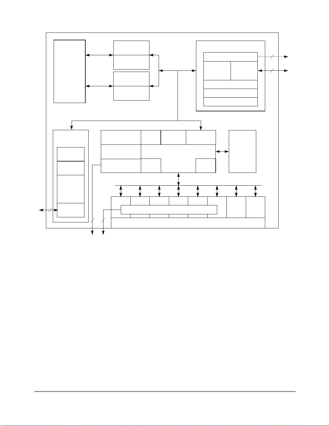
1.4.1 MPC860TBlock Diagram
The FEC, the embedded PowerPC core, the system interface unit (SIU), and the
communication processor module (CPM) all use the 32-bit internal bus in an
MPC860Timplementation. Figure 1-1 is a block diagram of the MPC860T. For
information on the other modules, refer to the
MPC860T UserÕs Manual
.
MOTOROLA
PRELIMINARYÑSUBJECT TO CHANGE WITHOUT NOTICE
Chapter 1. Overview
1-3
Page 14
Fr
eescale S
emiconduct
or
, I
Freescale Semiconductor, Inc.
For More Information On This Product,
Go to: www.freescale.com
nc...
Instruction
Bus
Embedded
PowerPC
Processor
Core
Fast
Ethernet
Controller
DMAs
FIFOs
Load/Store
Bus
Parallel Interface Port
4-KByte
Instruction Cache
Instruction MMU
4-KByte
Data Cache
Data MMU
Parallel I/O
Baud Rate
Generators
and UTOPIA
4 Timers
32-Bit RISC Controller
Timers
Unified
Bus
Interrupt
Controllers
and Program
ROM
System Interface Unit (SIU)
Memory Controller
Internal
Bus Interface
Unit
System Functions
PCMCIA-ATA Interface
Dual-Port RAM
MAC
External
Bus Interface
Unit
Real-Time Clock
Serial
and
DMA
Channels
10/100
Base-T
Media Access
Control
MII
SCC1 SCC2 SCC3 SCC4 SMC1 SMC2
Time Slot Assigner
Time Slot Assigner
I2CSPI
I2CSPI
Serial Interface
Serial Interface
Figure 1-1. MPC860T Block Diagram
The FEC complies with the IEEE 802.3 speciÞcation for 10- and 100-Mbps connectivity.
Full-duplex 100-Mbps operation is supported at system clock rates of 40 MHz and higher.
A 25-MHz system clock supports 10-Mbps operation or half-duplex 100-Mbps operation.
The implementation of bursting DMA reduces bus usage. Independent DMA channels for
accessing BDs and transmit and receive data minimize latency and FIFO depth
requirements.
Transmit and receive FIFOs further reduce bus usage by localizing all collisions to the FEC.
Transmit FIFOs maintain a full collision window of transmit frame data, eliminating the
need for repeated DMA over the system bus when collisions occur. On the receive side, a
full collision window of data is received before any receive data is transferred into system
memory, allowing the FIFO to be ßushed in the event of a runt or collided frame, with no
DMA activity. However, external memory for buffers and BDs is required; on-chip FIFOs
are designed only to compensate for collisions and for system bus latency.
Independent TxBD and RxBD rings in external memory allow nearly unlimited ßexibility
1-4
MPC860T (Rev. D) Fast Ethernet Controller Supplement
PRELIMINARYÑSUBJECT TO CHANGE WITHOUT NOTICE
MOTOROLA
Page 15
Fr
eescale S
emiconduct
or
, I
Freescale Semiconductor, Inc.
For More Information On This Product,
Go to: www.freescale.com
nc...
in memory management of transmit and receive data frames. External memory (DRAM) is
inexpensive, and because BD rings in external memory have no inherent size limitations,
memory management easily can be optimized to system needs.
1.4.2 SIU Interrupt ConÞguration
As shown in Figure 1-2, the SIU receives interrupts from internal sources, such as the FEC
and other modules and external pins, IRQ
[0Ð7].
System Interface Unit
IRQ[0Ð7]
Edge
Detector
Selector
DEC
SWT
Level 7
IRQ
NMI
GEN
0
NMI
DEC
TB
PIT
RTC
PCMCIA
CPM Interrupt
Controller
FEC
Level 6
Level 5
Level 4
Level 3
Level 2
Level 1
Level 0
PowerPC
IREQ
Interrupt Controller
Core
Debug
Debug
Figure 1-2. MPC860T Interrupt Structure
Note that MII_TXCLK is shared with IRQ7 and becomes active as soon as the ETHER_EN
bit in the Ethernet control register (ECNTRL) is set. IRQ7 must be masked in the system
interface unit (SIU).
1.5 Glueless System Design
A fundamental design goal of the MPC8xx family was ease of interface to other system
components. Examples of system design are located in the MPC860T userÕs manual.
MOTOROLA
PRELIMINARYÑSUBJECT TO CHANGE WITHOUT NOTICE
Chapter 1. Overview
1-5
Page 16

Fr
eescale S
emiconduct
or
, I
Freescale Semiconductor, Inc.
For More Information On This Product,
Go to: www.freescale.com
nc...
Figure 1-3 shows the glueless connection of the serial channels to physical layer framers
and transceivers.
MPC8xx
100Base-T
Transceiver
10Base-T
Transceiver
T1 Framer TDM
“7-wire” interface
MII
FEC
SCC1 (Ethernet)
SCC2 (QMC)
SCC3 (QMC)
RS-232
Transceiver
SCC4 (UART)
Figure 1-3. MPC860T Serial Configuration
1-6
MPC860T (Rev. D) Fast Ethernet Controller Supplement
PRELIMINARYÑSUBJECT TO CHANGE WITHOUT NOTICE
MOTOROLA
Page 17

Fr
eescale S
emiconduct
or
, I
Freescale Semiconductor, Inc.
For More Information On This Product,
Go to: www.freescale.com
nc...
Chapter 2
FEC External Signals
20
20
This chapter contains brief descriptions of the MPC860T FEC input and output signals in
their functional groups.
2.1 Signal Descriptions
The MPC860T system bus signals consist of all the lines that interface with the external
bus. Many of these lines perform different functions, depending on how the user assigns
them. The input and output signals, shown in Table 2-1, are identiÞed by their abbreviated
names.
Name
IRQ7
MII_TX_CLK
PD[15]
L1TSYNCA
MII_RXD[3]
PD[14]
L1RSYNCA
MII_RXD[2]
PD[13]
L1TSYNCB
MII_RXD[1]
Table 2-1. FEC Signal Descriptions
Pin
Number
W15 Interrupt request 7ÑThis input is one of the eight external lines that can request (by means
of the internal Interrupt Controller) a service routine from the core. See description of
MII_TXCLK for information about masking IRQ7
MII transmit clockÑInput clock that provides the timing reference for TX_EN, TXD, and
TX_ER. Note that MII_TXCLK becomes active as soon as the ETHER_EN bit in the Ethernet
control register (ECNTRL) is set. IRQ7
U17 General-purpose I/O port D bit 15ÑThis is bit 15 of the general-purpose I/O port D.
Transmit data sync signal for TDM channel A
MII receive data 3ÑInput signal RXD[3] represents bit 3 of the nibble of data to be
transferred from the PHY to the MAC when RX_DV is asserted.
V19 General-purpose I/O port D bit 14ÑThis is bit 14 of the general-purpose I/O port D.
Input receive data sync signal to the TDM channel A
MII receive data 2ÑInput signal RXD[2] represents bit 2 of the nibble of data to be
transferred from the PHY to the MAC when RX_DV is asserted.
V18 General-purpose I/O port D bit 13ÑThis is bit 13 of the general-purpose I/O port D.
Transmit data sync signal for TDM channel B
MII receive data 1ÑInput signal RXD[1] represents bit 1 of the nibble of data to be
transferred from the PHY to the MAC when RX_DV is asserted.
Description
.
must be masked in the system interface unit (SIU).
MOTOROLA
Chapter 2. FEC External Signals
PRELIMINARYÑSUBJECT TO CHANGE WITHOUT NOTICE
2-1
Page 18

Fr
eescale S
emiconduct
or
, I
Freescale Semiconductor, Inc.
For More Information On This Product,
Go to: www.freescale.com
nc...
Table 2-1. FEC Signal Descriptions (Continued)
Name
PD[12]
L1RSYNCB
MII_MDC
PD[11]
RXD3
MII_TX_ER
PD[10]
TXD3
MII_RXD[0]
PD[9]
RXD4
MII_TXD[0]
PD[8]
TXD4
MII_RX_CLK
PD[7]
RTS3
MII_RX_ER
PD[6]
RTS4
MII_RX_DV
Pin
Number
R16 General-purpose I/O port D bit 12ÑThis is bit 12 of the general-purpose I/O port D.
L1RSYNCBÑInput receive data sync signal to the TDM channel B.
MII management data clockÑOutput clock provides a timing reference to the PHY for data
transfers on the MDIO signal.
T16 General-purpose I/O port D bit 11ÑThis is bit 11 of the general-purpose I/O port D.
RXD3ÑReceive data for serial channel 3.
MII transmit errorÑOutput signal when asserted for one or more clock cycles while TX_EN is
asserted shall cause the PHY to transmit one or more illegal symbols. Asserting TX_ER has
no effect when operating at 10 Mbps or when TX_EN is negated.
W18 General-purpose I/O port D bit 10ÑThis is bit 10 of the general-purpose I/O port D.
TXD3ÑTransmit data for serial channel 3.
MII receive data 0ÑInput signal RXD[0] represents bit 0 of the nibble of data to be
transferred from the PHY to the MAC when RX_DV is asserted. In 10 Mbps serial mode,
RXD[0] is used and RXD[1Ð3] are ignored.
V17 General-purpose I/O port D bit 9ÑThis is bit 9 of the general-purpose I/O port D.
RXD4ÑReceive data for serial channel 4.
MII transmit data 0ÑOutput signal TXD[0] represents bit 0 of the nibble of data when TX_EN
is asserted and has no meaning when TX_EN is negated. In 10Mbps serial mode, TXD[0] is
used and TXD[1Ð3] are ignored.
W17 General-purpose I/O port D bit 8ÑThis is bit 8 of the general-purpose I/O port D.
TXD4ÑTransmit data for serial channel 4.
MII receive clockÑInput clock which provides a timing reference for RX_DV, RXD, and
RX_ER.
T15 General-purpose I/O port D bit 7ÑThis is bit 7 of the general-purpose I/O port D.
RTS3ÑActive-low request to send output indicates that SCC3 is ready to transmit data.
MII receive errorÑWhen Input signal RX_ER and RX_DV are asserted, the PHY has
detected an error in the current frame. When RX_DV is not asserted, RX_ER has no effect.
V16 General-purpose I/O port D bit 6ÑThis is bit 6 of the general-purpose I/O port D.
RTS4ÑActive low request to send output indicates that SCC4 is ready to transmit data.
MII receive data validÑWhen input signal RX_DV is asserted, the PHY is indicating that a
valid nibble is present on the MII. This signal shall remain asserted from the Þrst recovered
nibble of the frame through the last nibble. Assertion of RX_DV must start no later than the
SFD and exclude any EOF.
Description
PD[5]
REJECT2
MII_TXD[3]
2-2
U15 General-purpose I/O port D bit 5ÑThis is bit 5 of the general-purpose I/O port D.
Reject 2ÑThis input to SCC2 allows a CAM to reject the current Ethernet frame after it
determines the frame address did not match.
MII transmit data 3ÑOutput signal TXD[3] represents bit 3 of the nibble of data when TX_EN
is asserted and has no meaning when TX_EN is negated.
MPC860T (Rev. D) Fast Ethernet Controller Supplement
PRELIMINARYÑSUBJECT TO CHANGE WITHOUT NOTICE
MOTOROLA
Page 19

Fr
eescale S
emiconduct
or
, I
Freescale Semiconductor, Inc.
For More Information On This Product,
Go to: www.freescale.com
nc...
Table 2-1. FEC Signal Descriptions (Continued)
Name
PD[4]
REJECT3
MII_TXD[2]
PD[3]
REJECT4
MII_TXD[1]
MII_TX_EN V15 MII transmit enableÑOutput signal TX_EN indicates when there are valid nibbles being
MII_CRS B7 MII carrier receive senseÑWhen input signal CRS is asserted the transmit or receive
MII_COL H4 MII collisionÑInput signal COL is asserted upon detection of a collision, and will remain
MII_MDIO H18 MII management dataÑBidirectional signal, MDIO transfers control information between the
Pin
Number
U16 General-purpose I/O port D bit 4ÑThis is bit 4 of the general-purpose I/O port D.
Reject 3ÑThis input to SCC3 allows a CAM to reject the current Ethernet frame after it
determines the frame address did not match.
MII transmit data 2ÑOutput signal TXD[2] represents bit 2 of the nibble of data when TX_EN
is asserted and has no meaning when TX_EN is negated.
W16 General-purpose I/O port D bit 3ÑThis is bit 3 of the general-purpose I/O port D.
Reject 4ÑThis input to SCC4 allows a CAM to reject the current Ethernet frame after it
determines the frame address did not match.
MII transmit data 1ÑOutput signal TXD[1] represents bit 1 of the nibble of data when TX_EN
is asserted and has no meaning when TX_EN is negated.
presented on the MII. This signal is asserted with the Þrst nibble of preamble and is negated
prior to the Þrst TX_CLK following the Þnal nibble of the frame.
Note the following:
W
For 860T rev D.1, a 10-k
three-stated following reset until ECNTRL[FEC_PINMUX] is set.
For 860T rev D.2 and later, MII_TX_EN is a dedicated output and no pull-down resister is
required.
For 860T rev E.x (planned), MII_TX_EN resets to three-state with a weak internal
pull-down to ensure compatibility with 860 applications that may have tied SPARE3 (V15)
to VCC or GND. This pin will be 3-V only and must not be pulled up to +5 V.
medium is not idle. In the event of a collision, CRS will remain asserted through the duration
of the collision.
asserted while the collision persists. The behavior of this signal is not speciÞed for full-duplex
mode.
PHY and MAC. Transitions synchronously to MDC.
pull-down resistor must be used with MII_TX_EN, which is
Description
MOTOROLA
Chapter 2. FEC External Signals
PRELIMINARYÑSUBJECT TO CHANGE WITHOUT NOTICE
2-3
Page 20

Fr
eescale S
emiconduct
or
, I
Freescale Semiconductor, Inc.
For More Information On This Product,
Go to: www.freescale.com
nc...
2-4
MPC860T (Rev. D) Fast Ethernet Controller Supplement
PRELIMINARYÑSUBJECT TO CHANGE WITHOUT NOTICE
MOTOROLA
Page 21

Fr
eescale S
emiconduct
or
, I
Freescale Semiconductor, Inc.
For More Information On This Product,
Go to: www.freescale.com
nc...
Chapter 3
Fast Ethernet Controller Operation
30
30
This chapter discusses the operation of the FEC.
3.1 Transceiver Connection
The FEC supports both an MII interface for 10/100 Mbps Ethernet and a seven-wire serial
interface for 10-Mbps Ethernet. The interface mode is selected by
R_CNTRL[MII_MODE], described in Section 6.2.20, ÒReceive Control Register
(R_CNTRL).Ó Table 3-1 shows the 18 MII interface signals that are deÞned by the 802.3
standard.
Table 3-1. MII Signals
Signal Description FEC Signal Name
Transmit clock TX_CLK
Transmit enable TX_EN
Transmit data TXD[3:0]
Transmit error TX_ER
Collision COL
Carrier sense CRS
Receive clock RX_CLK
Receive enable RX_DV
Receive data RXD[3:0]
Receive error RX_ER
Management channel clock MDC
Management channel serial data MDIO
Serial-mode connections to the external transceiver are shown in Table 3-2.
MOTOROLA
Chapter 3. Fast Ethernet Controller Operation
PRELIMINARYÑSUBJECT TO CHANGE WITHOUT NOTICE
3-1
Page 22

Fr
eescale S
emiconduct
or
, I
Freescale Semiconductor, Inc.
For More Information On This Product,
Go to: www.freescale.com
nc...
Table 3-2. Serial Mode Connections to the External Transceiver
Signal Description FEC Signal Name
Transmit clock TX_CLK
Transmit enable TX_EN
Transmit data TXD0
Collision COL
Receive clock RX_CLK
Receive enable RX_DV
Receive Data RXD0
Unused 860T inputsÑTie to ground RX_ER, CRS, RXD[3:1]
Unused 860T outputsÑIgnore TX_ER, TXD[3:1], MDC, MDIO
3.2 FEC Frame Transmission
FEC transmissions require almost no host intervention. When the software driver sets the
ETHER_EN bit in the Ethernet control register (ECNTRL) and the X_DES_ACTIVE bit
in the CSR TxBD active register (X_DES_ACTIVE), the FEC is enabled and fetches the
Þrst TxBD. If the user has a frame ready to transmit, a DMA transfer of the transmit data
buffers begins immediately.
A 512-bit collision window of transmit data is sent to the transmit FIFO before transmission
begins. If the line is not busy, the MAC transmit logic asserts TX_EN and sends the
preamble sequence, the start frame delimiter (SFD), and then the frame information. If the
line is busy, the controller waits for the carrier sense signal, CRS, to remain inactive for 60
bit times. Transmission begins after an additional 36 bit times (96 bit times after CRS
became inactive).
If a collision occurs during the transmit frame, the FEC follows the speciÞed backoff
procedures and tries retransmitting the frame until the retry limit threshold is reached. The
FEC stores the Þrst 64 bytes of the transmit frame in internal RAM so that they do not have
to be retrieved from system memory in case of a collision. This improves bus usage and
latency in case the backoff timer output causes a need for an immediate retransmission.
When the end of the current BD is reached and TxBD[L] is set, the frame check sequence
(32-bit CRC) is appended (if TxBD[TC] = 1) and TX_EN is negated. After the frame check
sequence is sent, the FEC writes the frame status bits into the BD and clears the R bit. When
the end of the current BD is reached and the L bit is not set (a frame consists of multiple
buffers), only the R bit is cleared. Short frames are automatically padded by the transmit
logic.
A transmit frame length exceeding the value set for MAX_FRAME_LENGTH in the
receive hash register (R_HASH) generates a babbling transmit interrupt
3-2 MPC860T (Rev. D) Fast Ethernet Controller Supplement MOTOROLA
PRELIMINARYÑSUBJECT TO CHANGE WITHOUT NOTICE
Page 23

Fr
eescale S
emiconduct
or
, I
Freescale Semiconductor, Inc.
For More Information On This Product,
Go to: www.freescale.com
nc...
(I_EVENT[BABT] = 1); however, the entire frame is sent (no truncation). Whether buffer
or frame interrupts can be generated is determined by I_MASK settings.
To pause transmission, set the graceful transmit stop bit, X_CNTRL[GTS]. When GTS is
set, the FEC transmitter stops immediately if no transmission is in progress or continues
transmission until the current frame either Þnishes or terminates with a collision. The GRA
interrupt occurs when the graceful transmit stop operation completes. When GTS is
cleared, the FEC resumes transmission with the next frame.
The FEC transmits bytes lsb Þrst.
3.3 FEC Frame Reception
FEC reception requires almost no host intervention. The FEC can perform address
recognition, CRC checking, short-frame checking, and maximum frame-length checking.
When the software driver sets ECNTRL[ETHER_EN] and R_DES_ACTIVE in the CSR
RxBD active register (R_DES_ACTIVE), the FEC receiver is enabled and immediately
starts processing receive frames. When RX_DV is asserted, the receiver Þrst checks for a
valid preamble/SFD (start frame delimiter) header, which is stripped and the frame is
processed by the receiver. If a valid header is not found, the frame is ignored.
In serial mode, the Þrst 16 bit times of RX_D0 after RX_DV (RENA) is asserted are
ignored. Following the Þrst 16 bit times the data sequence is checked for alternating ones
and zeros.
¥ If a 11 or 00 sequence is detected during bit times 17 to 21, the rest of the frame is
ignored.
¥ After bit time 21, the data sequence is monitored for a valid SFD (11). If a 00 is
detected, the frame is rejected. If a 11 is detected, the preamble/SFD sequence is
complete.
In MII mode, the receiver checks for at least one byte matching the SFD. Zero or more
preamble bytes may occur, but if a 00 sequence is detected before the SFD byte, the frame
is ignored.
After the Þrst eight bytes of the frame are passed to the receive FIFO, the FEC performs
address recognition on the frame.
As soon as a collision window (64 bytes) of data is received and if address recognition has
not rejected the frame, the FEC starts transferring the incoming frame to the RxBDÕs
associated buffer. If the frame is a too short (due to collision) or is rejected by address
recognition, no receive buffers are Þlled. Thus, no collision frames are presented to the user,
except for any late collisions, which indicate serious LAN problems. When the data buffer
has been Þlled, the FEC clears RxBD[E] and generates an RXB interrupt (if
I_MASK[RBIEN] is set). If the incoming frame exceeds the length of the data buffer, the
FEC fetches the next RxBD in the table and, if it is empty, continues transferring the rest
MOTOROLA Chapter 3. Fast Ethernet Controller Operation 3-3
PRELIMINARYÑSUBJECT TO CHANGE WITHOUT NOTICE
Page 24

Fr
eescale S
emiconduct
or
, I
Freescale Semiconductor, Inc.
For More Information On This Product,
Go to: www.freescale.com
nc...
of the frame to the associated data buffer.
R_BUFF_SIZE[R_BUFF_SIZE] determines buffer length, which should be at least 128
bytes. R_BUFF_SIZE must be quad-word (16-byte) aligned.
During reception, the FEC checks for a frame that is either too short or too long. When the
frame ends (CRS is negated), the receive CRC Þeld is checked and written to the data
buffer. The data length written to the last BD in the Ethernet frame is the length of the entire
frame. Frames smaller than 64 bytes are not accessed and are rejected in hardware with no
impact on system bus usage.
Receive frames are not truncated if they exceed MAX_FRAME_LENGTH bytes, however
the babbling receive error interrupt occurs (I_EVENT[BABR] = 1) and RxBD[LG] is set.
When the receive frame is complete, the FEC sets RxBD[L], writes the other frame status
bits into the RxBD, and clears the E bit. The FEC next generates a maskable interrupt
(I_EVENT[RFINT] maskable by I_MASK[RFIEN]), indicating that a frame has been
received and is in memory. The FEC then waits for a new frame.
The FEC receives serial data lsb Þrst.
3.4 CAM Interface
In addition to the FEC address recognition logic, an external CAM may be used for frame
reject with no additional pins other than the MII interface pins. For more information on
the CAM interface refer to Using MotorolaÕs Fast Static RAM CAMs with the MPC860TÕs
Media Independent Interface application note.
3.5 FEC Command Set
The FEC does not support commands as found in the CPM channels. After the FEC is
initialized and enabled, it operates autonomously. Typically, aside from initialization, the
driver only writes to R_DES_ACTIVE, X_DES_ACTIVE, and I_EVENT during
operation.
3.6 Ethernet Address Recognition
The FEC Þlters the received frames based on destination address (DA) typeÑindividual
(unicast), group (multicast), or broadcast (all-ones group address). The difference between
an individual address and a group address is determined by the I/G bit in the destination
address Þeld. Figure 3-1 shows a ßowchart for address recognition on received frames.
If the DA is the individual (unicast) type of address, the FEC compares the destination
address Þeld of the received frame with the 48-bit address that the user programs in the
ADDR_LOW and ADDR_HIGH.
If the DA is the group type of address, the FEC determines whether the group address is a
3-4 MPC860T (Rev. D) Fast Ethernet Controller Supplement MOTOROLA
PRELIMINARYÑSUBJECT TO CHANGE WITHOUT NOTICE
Page 25

Fr
eescale S
emiconduct
or
, I
Freescale Semiconductor, Inc.
For More Information On This Product,
Go to: www.freescale.com
nc...
broadcast address. If it is, the frame is accepted unconditionally; otherwise (multicast
address) a hash table lookup is performed using the 64-entry hash table deÞned in the hash
table registers.
In promiscuous mode (R_CNTRL[PROM] = 1), the FEC receives all the incoming frames
regardless of their address. In this mode the DA lookup is still performed and the MISS bit
in the RxBD is set accordingly. If address recognition did not achieve a match, the frame is
received with RxBD[MISS] set. If address recognition achieves a match the frame is
received without the MISS bit being set.
Check Address
Receive Frame
Receive Frame
Tr u e
Tr u e
I/G Address
?
G
Broadcast
Address
?
False
Hash Match
?
False
Promiscuous
Mode
?
False
(R_CNTRL[PROM] = 1)
I
Perfect Match
?
True (R_CNTRL[PROM] = 1)
Tr u eFalse
Receive Frame
Receive Frame
Set Miss Bit
Discard Frame
Figure 3-1. Ethernet Address Recognition Flowchart
3.7 Hash Table Algorithm
This section discusses the hash table process used in group hash Þltering. When the FEC
receives a frame with the destination address I/G bit set, the 48-bit address is mapped into
one of 64 bins, represented by the 64 bits in the two hash table registers. This is performed
by passing the 48-bit address through the on-chip 32-bit CRC generator and selecting 6 bits
MOTOROLA Chapter 3. Fast Ethernet Controller Operation 3-5
PRELIMINARYÑSUBJECT TO CHANGE WITHOUT NOTICE
Page 26

Fr
eescale S
emiconduct
or
, I
Freescale Semiconductor, Inc.
For More Information On This Product,
Go to: www.freescale.com
nc...
of the CRC-encoded result to generate a number between 0 and 63.
Bit 31 of the CRC result selects HASH_TABLE_HIGH (bit 31 = 1) or
HASH_TABLE_LOW (bit 31 = 0). Bits 30Ð26 of the CRC result select the bit in the
selected register. If that bit is set in the hash table, the frame is accepted; otherwise, it is
rejected. The result is that if eight group addresses are stored in the hash table and random
group addresses are received, the hash table prevents roughly 56/64 (or 87.5%) of the group
address frames from reaching memory. The processor must further Þlter those that reach
memory to determine if they truly contain one of the eight preferred addresses.
The effectiveness of the hash table declines as the number of addresses increases.
The user must initialize the hash table registers. The FEC does not support the
ADDRESS
the hash for a particular address in software or use the
off-line CPM channel, retrieve the result, and use it to program the FEC hash table registers.
The CRC32 polynomial to use in computing the hash is as follows:
command, which can be used in CPM ethernet controllers. The user may compute
SET GROUP ADDRESS command in an
X32X26X23X22X16X12X11X10X8X7X5X4X2X 1++++++++++++++
SET GROUP
3.8 Inter-Packet Gap Time
The minimum inter-packet gap time for back-to-back transmission is 96 bit times. After
completing a transmission or after the backoff algorithm completes, the transmitter waits
for the carrier sense signal (CRS) to be negated before starting its 96 bit time IPG counter.
Frame transmission may begin 96 bit times after CRS is negated if it stays negated for at
least 60 bit times. If CRS asserts during the last 36 bit times it is ignored and a collision
occurs.
The receiver receives back-to-back frames with a minimum spacing of at least 28 bit times.
If an interrupted gap between receive frames is less than 28 bit times, the receiver may
discard the next frame.
3.9 Collision Handling
If a collision occurs during frame transmission, the FEC continues transmitting for at least
32 bit times, sending a JAM pattern of 32 ones. If the collision occurs during the preamble
sequence, the JAM pattern is sent after the preamble sequence.
If a collision occurs within 64 byte times, the retry process is initiated. The transmitter waits
a random number of slot times. A slot time is 512 bit times. If a collision occurs after 64
byte times, no retransmission is performed and the end of frame buffer is closed with an LC
error indication.
3-6 MPC860T (Rev. D) Fast Ethernet Controller Supplement MOTOROLA
PRELIMINARYÑSUBJECT TO CHANGE WITHOUT NOTICE
Page 27

Fr
eescale S
emiconduct
or
, I
Freescale Semiconductor, Inc.
For More Information On This Product,
Go to: www.freescale.com
nc...
3.10 Internal and External Loopback
The FEC supports Both internal and external loopback. In loopback mode, both FIFOs are
used and the FEC operates in full-duplex fashion. Both internal and external loopback are
conÞgured through R_CNTRL[LOOP, DRT].
For internal loopback, set LOOP = 1 and DRT = 0. TX_EN and TX_ER are not asserted
during internal loopback.
For external loopback, set LOOP = 0 and DRT = 0. ConÞgure the external transceiver for
loopback.
3.11 Ethernet Error-Handling Procedure
The FEC reports frame reception and transmission error conditions using the FEC BDs and
the I_EVENT register.
3.11.1 Transmission Errors
Table 3-3 describes transmission errors.
Table 3-3. Transmission Errors
Error Description
Transmitter
Underrun
Carrier Sense
Lost during
Frame
Transmission
Retransmission
Attempts Limit
Expired
Late Collision When this error occurs, the FEC stops sending. All remaining buffers for that frame are then ßushed
Heartbeat Some transceivers have a self-test feature called heartbeat or signal-quality error. To signify a good
If this error occurs, the FEC sends 32 bits that ensure a CRC error and stops transmitting. All
remaining buffers for that frame are then ßushed and closed, with the UN bit set in the last TxBD for
that frame. The FEC continues to the next TxBD and begins transmitting the next frame.
When this error occurs and no collision is detected in the frame, the FEC sets the CSL bit in the last
TxBD for this frame. The frame is sent normally. No retries are performed as a result of this error.
The CSL bit is not set if X_CNTRL[FDEN] = 1, regardless of the state of CRS.
When this error occurs, the FEC terminates transmission. All remaining buffers for that frame are
then ßushed and closed, with the RL bit set in the last TxBD for that frame. The FEC then continues
to the next TxBD and begins sending the next frame.
and closed, with the LC bit set in the last TxBD for that frame. The FEC then continues to the next
TxBD and begins sending the next frame.
Note: The deÞnition of what constitutes a late collision is hard-wired in the FEC.
self-test, the transceiver indicates a collision within 20 clocks after the FEC sends a frame. This
heartbeat condition does not imply a real collision, but that the transceiver seems to work properly.
If X_CNTRL[HBC] = 1, X_CNTRL[FDEN]=0, and a heartbeat condition is not detected after a frame
transmission, a heartbeat error occursÑthe FEC closes the buffer, sets TxBD[HB], and generates
the HBERR interrupt if it is enabled.
3.11.2 Reception Errors
Table 3-4 describes reception errors.
MOTOROLA Chapter 3. Fast Ethernet Controller Operation 3-7
PRELIMINARYÑSUBJECT TO CHANGE WITHOUT NOTICE
Page 28

Fr
eescale S
emiconduct
or
, I
Freescale Semiconductor, Inc.
For More Information On This Product,
Go to: www.freescale.com
nc...
Table 3-4. Reception Errors
Error Description
Overrun Error The FEC maintains an internal FIFO for receiving data. If a receiver FIFO overrun occurs, the FEC
Non-Octet
Error
(Dribbling Bits)
CRC Error
Frame Length
Violation
closes the buffer and sets RxBD[OV].
The FEC handles up to seven dribbling bits when the receive frame terminates nonoctet aligned and
it checks the CRC of the frame on the last octet boundary. If there is a CRC error, the frame nonoctet
aligned (NO) error is reported in the RxBD. If there is no CRC error, no error is reported.
When a CRC error occurs with no dribbling bits, the FEC closes the buffer and sets RxBD[CR]. CRC
checking cannot be disabled, but the CRC error can be ignored if checking is not required.
When the receive frame length exceeds R_HASH[MAX_FRAME_LENGTH], I_EVENT[BABR] is set
indicating babbling receive error, and the LG bit in the end of frame RxBD is set.
Note: Receive frames exceeding 2047 bytes are truncated.
3-8 MPC860T (Rev. D) Fast Ethernet Controller Supplement MOTOROLA
PRELIMINARYÑSUBJECT TO CHANGE WITHOUT NOTICE
Page 29

Fr
eescale S
emiconduct
or
, I
Freescale Semiconductor, Inc.
For More Information On This Product,
Go to: www.freescale.com
nc...
Chapter 4
Parallel I/O Ports
40
40
This chapter shows how to use port D pin multiplexing to support Fast Ethernet controller
(FEC) operations.
4.1 Port D Pin Functions
Each of the 13 port D pins is independently conÞgured as a general-purpose I/O pin if the
corresponding port D pin assignment register (PDPAR) bit is cleared. Each pin is
conÞgured as a dedicated on-chip peripheral pin if the corresponding PDPAR bit is set.
Refer to Table 4-1 for the default description of all port D pin options.
When the port pin is conÞgured as a general-purpose I/O pin, the signal direction for that
pin is determined by the corresponding control bit in the port D data direction register
(PDDIR). The port I/O pin is conÞgured as an input if the corresponding PDDIR bit is
cleared; it is conÞgured as an output if the corresponding PDDIR bit is set. All PDPAR bits
and PDDIR pins are cleared on total system reset, conÞguring all port D pins as generalpurpose input pins.
PD[13:8] peripheral functions (RXD3, TXD3, RXD4, TXD4) are alternately available on
PA[11:8]. PD[7:5], and PD12 peripheral functions (R
alternately available on PC[13:12] and PC6. Functions REJECT3
when MII mode is used. The peripheral functions L1TSYNCB, L1TSYANCA and
L1RSYNCA found on PD[15:13] are alternatively available on PC7, PC5, and PC4.
Note: The reserved bits of the PDPAR must be written with zeros. Failure to do so may
result in one or more of the following:
¥ No events on SCC3 and SCC4.
¥ No events on any CPM peripheral.
¥ Pin multiplexing of Port D will not be as expected
TS3, RTS4, and L1RSYNCB) are
and REJECT4 are lost
MOTOROLA Chapter 4. Parallel I/O Ports 4-1
PRELIMINARYÑSUBJECT TO CHANGE WITHOUT NOTICE
Page 30

Fr
eescale S
emiconduct
or
, I
Freescale Semiconductor, Inc.
For More Information On This Product,
Go to: www.freescale.com
nc...
Table 4-1 shows the port D pin assignments.
Table 4-1. Port D Pin Assignment
Signal Function
Signal
PDPAR = 0
PDDIR=0 PDDIR=1
PD15 PORT D15 L1TSYNCA MII-RXD3 (I) L1TSYNCA=GND
PD14 PORT D14 L1RSYNCA MII-RXD2 (I) L1RSYNCA=GND
PD13 PORT D13 L1TSYNCB MII-RXD1 (I) L1TSYNCB=GND
PD12 PORT D12 L1RSYNCB MII-MDC (O) L1RSYNCB=GND
PD11 PORT D11 RXD3 MII-TX-ERR (O) RXD3 = GND
PD10 PORT D10 TXD3 MII-RXD0 (I) Ñ
PD9 PORT D9 RXD4 MII-TXD0 (O) RXD4 = GND
PD8 PORT D8 TXD4 MII-RX_CLK (I) Ñ
PD7 PORT D7 RTS3\MII-RX-ERR(I) Ñ
PD6 PORT D6 RTS4 MII-RXDV (I) Ñ
PD5 PORT D5 REJECT2 MII-TXD3 (O) REJECT2=VDD
PD4 PORT D4 REJECT3 MII-TXD2 (O) REJECT3=VDD
PD3 PORT D3 REJECT4 MII-TXD1 (O) REJECT4=VDD
PDPAR=1
Input to On-Chip
4.1.1 Port D Registers
Port D has three memory-mapped, read/write, 16-bit control registers.
4.1.2 Enabling MII Mode
To enable MII mode, do the following:
1. Write 0x1FFF to PDPAR.
2. Write 0x1FFF to PDDIR.
Peripherals
4-2 MPC860T (Rev. D) Fast Ethernet Controller Supplement MOTOROLA
PRELIMINARYÑSUBJECT TO CHANGE WITHOUT NOTICE
Page 31

Fr
eescale S
emiconduct
or
, I
Freescale Semiconductor, Inc.
For More Information On This Product,
Go to: www.freescale.com
nc...
Chapter 5
SDMA Bus Arbitration and Transfers
50
50
This chapter describes SDMA functions speciÞc to the MPC860T, particularly where the
functionality differs from the MPC860. For a full discussion of SDMA bus arbitration and
transfers, refer to the MPC860 PowerQUICC UserÕs Manual.
5.1 Overview
The MPC860T has two arbitration levels to considerÑaccesses to the SDMA hardware and
accesses to the 60x bus. As shown in Figure 5-1, if the CPM and the 100BASE-T module
attempt to access the SDMA simultaneously, the CPM wins the Þrst access. If both continue
to request the SDMA hardware, control alternates between the two.
Other cycle SDMA cycle
CLK
TS
TA
SDMA internally
requests the bus
Figure 5-1. SDMA Bus Arbitration
The priority of the SDMA on the 60x bus is programmed in SDCR[RAID], described in
Section 5.2.1, ÒSDMA ConÞguration Register (SDCR).Ó
Other cycle
5.2 The SDMA Registers
This supplement describes the portions of the SDMA that differ from the MPC860. For a
thorough description of the SDMA, refer to the MPC860 PowerQUICC UserÕs Manual.
The SDMA channels share a conÞguration register, address register, and status register, and
are controlled by the conÞguration of the SCCs, SMCs, SPI, and I
MOTOROLA Chapter 5. SDMA Bus Arbitration and Transfers 5-1
PRELIMINARYÑSUBJECT TO CHANGE WITHOUT NOTICE
2
C controllers.
Page 32

Fr
eescale S
emiconduct
or
, I
Freescale Semiconductor, Inc.
For More Information On This Product,
Go to: www.freescale.com
nc...
5.2.1 SDMA ConÞguration Register (SDCR)
The SDMA conÞguration register (SDCR), shown in Figure 5-2, is used to conÞgure all 16
SDMA channels. It is always read/write in supervisor mode, although writing to the SDCR
is not recommended unless the CPM is disabled. SDCR interacts with the DMA controllers
in the FEC. Refer to the MPC860 PowerQUICC UserÕs Manual for more information.
Bit 0 1 2 3 4 5 6 7 8 9 10 11 12 13 14 15
Field Ñ
Reset 0000_0000_0000_0000
R/W R/W
Address (IMMR & 0xFFFF0000) + 0x030
Bit 16 17 18 19 20 21 22 23 24 25 26 27 28 29 30 31
Field Ñ FRZ Ñ FAID RAID
Reset 0 0 00_0000_0000 00 00
R/W R R/W R R/W R/W
Address (IMMR & 0xFFFF0000) + 0x030
Figure 5-2. SDMA Configuration Register (SDCR)
Table 5-1 describes SDCR Þelds.
Table 5-1. SDCR Field Descriptions
Bits Name Description
0Ð16 Ñ Reserved. These bits are reserved and should be cleared.
17 FRZ Freeze. Determines the action to be taken when the FRZ signal is asserted. The SDMA negates
19Ð27 Ñ Reserved, should be cleared for typical applications.
28Ð29 FAID FEC arbitration ID. Determines FEC arbitration priority for the U bus; 00 for typical applications.
30Ð31 RAID RISC controller arbitration ID. Determines the SDMA channel arbitration ID, which establishes the
BR
and keeps it that way until the FRZ signal is negated or reset occurs.
0 The SDMA channels ignore the FRZ signal.
1 The SDMA channels freeze on the next bus cycle.
00 Priority 6 (highest)
01 Priority 5
10 Priority 2
11 Priority 1 (lowest)
priority level of bus arbitration among modules that can become master of the U bus (01 for
typical applications). The instruction cache, data cache, SIU, and SDMAs compete for bus
mastership. Arbitration IDs for all other bus masters are internally Þxed.
00 Priority 6 (highest)
01 Priority 5
10 Priority 2
11 Priority 1 (lowest)
5-2 MPC860T (Rev. D) Fast Ethernet Controller Supplement MOTOROLA
PRELIMINARYÑSUBJECT TO CHANGE WITHOUT NOTICE
Page 33

Fr
eescale S
emiconduct
or
, I
Freescale Semiconductor, Inc.
For More Information On This Product,
Go to: www.freescale.com
nc...
Chapter 6
Programming Model
60
60
This chapter gives an overview of the MPC860T implementation of the Fast Ethernet
controller (FEC) registers, buffer descriptors (BDs), and initialization.
6.1 Overview
The FEC software model is similar to that used by the 10-Mbps Ethernet implemented on
the MPC860 core device. To support higher data rates, the FEC has a different internal
architecture, which changes the programming model slightly. However, efforts have been
taken to minimize the differences required by the interrupt handlers. The FECÕs registers
are very different from those of the CPM-based internal Ethernet controller.
The FEC is programmed by a combination of control/status registers (CSRs) and BDs. The
CSRs are used for mode control and to extract global status information. The BDs are used
to pass data buffers and related buffer information between hardware and software.
Some registers are located in on-chip RAM. All on-chip registers, whether located in RAM
or in hardware, must be accessed using big-endian mode, therefore, descriptions in this
chapter assume big-endian byte ordering. There is no support for little-endian in the FEC.
6.2 Parameter RAM
Table 6-1 brießy describes each enter in the FEC parameter RAM.
Table 6-1. FEC Parameter RAM Memory Map
Address Name Description Section
0xE00 ADDR_LOW Lower 32 bits of address 6.2.1
0xE04 ADDR_HIGH Upper 16 bits of address 6.2.2
0xE08 HASH_TABLE_HIGH Upper 32 bits of hash table 6.2.3
0xE0C HASH_TABLE_LOW Lower 32 bits of hash table 6.2.4
0xE10 R_DES_START Pointer to beginning of RxBD ring 6.2.5
0xE14 X_DES_START Pointer to beginning of TxBD ring 6.2.6
0xE18 R_BUFF_SIZE Receive buffer size 6.2.7
MOTOROLA Chapter 6. Programming Model 6-1
PRELIMINARYÑSUBJECT TO CHANGE WITHOUT NOTICE
Page 34

Fr
eescale S
emiconduct
or
, I
Freescale Semiconductor, Inc.
For More Information On This Product,
Go to: www.freescale.com
nc...
Table 6-1. FEC Parameter RAM Memory Map (Continued)
Address Name Description Section
0xE40 ECNTRL Ethernet control register 6.2.8
0xE44 IEVENT Interrupt event register 6.2.9
0xE48 IMASK Interrupt mask register 6.2.9
0xE4C IVEC Interrupt level and vector status 6.2.10
0xE50 R_DES_ACTIVE Receive ring updated ßag 6.2.11
0xE54 X_DES_ACTIVE Transmit ring updated ßag 6.2.12
0xE80 MII_DATA MII data register 6.2.13
0xE84 MII_SPEED MII speed register 6.2.14
0xECC R_BOUND End of FIFO RAM (read-only) 6.2.15
0xED0 R_FSTART Receive FIFO start address 6.2.16
0xEE4 X_WMRK Transmit Watermark 6.2.17
0xEEC X_FSTART Transmit FIFO start address 6.2.18
0xF34 FUN_CODE Function code to SDMA 6.2.19
0xF44 R_CNTRL Receive control register 6.2.20
0xF48 R_HASH Receive hash register 6.2.21
0xF84 X_CNTRL Transmit control register 6.2.22
6.2.1 RAM Perfect Match Address Low Register (ADDR_LOW)
The ADDR_LOW register, shown in Figure 6-1, is written by and must be initialized by the
user. It contains the lower 32 bits of the 48-bit address used in the address recognition
process to compare with the destination address Þeld of the receive frames.
Bits 0 1 2 3 4 5 6 7 8 9 10 11 12 13 14 15
Field ADDR_LOW BYTE 0 ADDR_LOW BYTE 1
Reset UndeÞned
R/W Read/write
Addr 0xE00
Bits 16 17 18 19 20 21 22 23 24 25 26 27 28 29 30 31
Field ADDR_LOW BYTE 2 ADDR_LOW BYTE 3
Reset UndeÞned
R/W Read/write
Addr 0xE02
Figure 6-1. ADDR_LOW Register
6-2 MPC860T (Rev. D) Fast Ethernet Controller Supplement MOTOROLA
PRELIMINARYÑSUBJECT TO CHANGE WITHOUT NOTICE
Page 35

Fr
eescale S
emiconduct
or
, I
Freescale Semiconductor, Inc.
For More Information On This Product,
Go to: www.freescale.com
nc...
Table 6-2 describes the ADDR_LOW Þelds.
Table 6-2. ADDR_LOW Field Descriptions
Bits Name Description
0Ð31 ADDR_LOW Bytes in the 6-byte address: 0 (bits 0Ð7), 1 (bits 8Ð15), 2 (bits 16Ð23) and 3 (bits 24Ð31)
6.2.2 RAM Perfect Match Address High (ADDR_HIGH)
The ADDR_HIGH register, shown in Figure 6-2, is written by and must be initialized by
the user. It contains bytes 4 and 5 of the 6-byte address used to compare with the destination
address Þeld of the receive frames. Byte 0 is the Þrst byte sent at the start of the frame.
Bits 0 1 2 3 4 5 6 7 8 9 10 11 12 13 14 15
Field ADDR_HIGH BYTE 4 ADDR_HIGH BYTE 5
Reset UndeÞned
R/W Read/write
Addr 0xE04
Bits 16 17 18 19 20 21 22 23 24 25 26 27 28 29 30 31
Field Ñ
Reset UndeÞned
R/W Read/write
Addr 0xE06
Figure 6-2. ADDR_HIGH Register
Table 6-3 describes the ADDR_HIGH Þelds.
Table 6-3. ADDR_HIGH Field Descriptions
Bits Name Description
0Ð15 ADDR_HIGH Bytes of the 6-byte address: 4 (bits 0Ð7) and 5 (bits 8Ð15)
16Ð31 Ñ Reserved. Should be cleared by the host processor.
6.2.3 RAM Hash Table High (HASH_TABLE_HIGH)
The HASH_TABLE_HIGH register, shown in Figure 6-3, contains the upper 32 bits of the
64-bit hash table used in address recognition for receive frames with a multicast address. It
is written by and must be initialized by the user
MOTOROLA Chapter 6. Programming Model 6-3
PRELIMINARYÑSUBJECT TO CHANGE WITHOUT NOTICE
Page 36

Fr
eescale S
emiconduct
or
, I
Freescale Semiconductor, Inc.
For More Information On This Product,
Go to: www.freescale.com
nc...
Bits 0 1 2 3 4 5 6 7 8 9 10 11 12 13 14 15
Field HASH_HIGH
Reset UndeÞned
R/W Read/write
Addr 0xE08
Bits 16 17 18 19 20 21 22 23 24 25 26 27 28 29 30 31
Field HASH_HIGH
Reset UndeÞned
R/W Read/write
Addr 0xE0A
Figure 6-3. HASH_TABLE_HIGH Register
Table 6-4 describes HASH_TABLE_HIGH Þelds.
Table 6-4. HASH_TABLE_HIGH Field Descriptions
Bits Name Description
0Ð31 HASH_HIGH Contains the upper 32 bits of the 64-bit hash table used in address recognition for receive
frames with a multicast address. HASH_HIGH[0] contains hash index bit 63.
HASH_HIGH[31] contains hash index bit 32.
6.2.4 RAM Hash Table Low (HASH_TABLE_LOW)
The HASH_TABLE_LOW register, shown in Figure 6-4, contains the lower 32 bits of the
64-bit hash table used in the address recognition process for receive frames with a multicast
address. It is written by and must be initialized by the user.
Bits 0 1 2 3 4 5 6 7 8 9 10 11 12 13 14 15
Field HASH_LOW
Reset UndeÞned
R/W Read/write
Addr 0xE0C
Bits 16 17 18 19 20 21 22 23 24 25 26 27 28 29 30 31
Field HASH_LOW
Reset UndeÞned
R/W Read/write
Addr 0xE0E
Figure 6-4. HASH_TABLE_LOW Register
6-4 MPC860T (Rev. D) Fast Ethernet Controller Supplement MOTOROLA
PRELIMINARYÑSUBJECT TO CHANGE WITHOUT NOTICE
Page 37

Fr
eescale S
emiconduct
or
, I
Freescale Semiconductor, Inc.
For More Information On This Product,
Go to: www.freescale.com
nc...
Table 6-5 describes HASH_TABLE_LOW Þelds.
Table 6-5. HASH_TABLE_LOW Field Descriptions
Bits Name Description
0Ð31 HASH_LOW Contains the lower 32 bits of the 64-bit hash table used in address recognition for receive
frames with a multicast address. HASH_LOW[0] contains hash index bit 31. HASH_LOW[31]
contains hash index bit 0.
6.2.5 Beginning of RxBD Ring (R_DES_START)
The R_DES_START register, shown in Figure 6-5, is like the RBASE register used by
other protocols. It provides a pointer to the start of the circular RxBD queue in external
memory. This pointer should be quad-word aligned. Bits 30 and 31 should be written to 0
by the user; hardware ignores non-zero values in these bits. This register is written by the
user, is not reset, and must be initialized by the user.
Bits 0 1 2 3 4 5 6 7 8 9 10 11 12 13 14 15
Field R_DES_START
Reset UndeÞned
R/W Read/write
Addr 0xE10
Bits 16 17 18 19 20 21 22 23 24 25 26 27 28 29 30 31
Field R_DES_START 00
Reset UndeÞned
R/W Read/write
Addr 0xE12
Figure 6-5. R_DES_START Register
Table 6-6 describes R_DES_START Þelds.
Table 6-6. R_DES_START Field Descriptions
Bits Name Description
0Ð29 R_DES_START Pointer to start of RxBD queue.
30Ð31 Ñ Reserved. Should be written to zero by the host processor.
6.2.6 Beginning of TxBD Ring (X_DES_START)
The X_DES_START register, shown in Figure 6-6, is like the TBASE register used by other
protocols. It provides a pointer to the start of the circular TxBD queue in external memory.
This pointer should be quad-word aligned. Bits 30 and 31 should be cleared by the user;
hardware ignores non-zero values in these bits. It is written by the user, is not reset, and
must be initialized by the user.
MOTOROLA Chapter 6. Programming Model 6-5
PRELIMINARYÑSUBJECT TO CHANGE WITHOUT NOTICE
Page 38

Fr
eescale S
emiconduct
or
, I
Freescale Semiconductor, Inc.
For More Information On This Product,
Go to: www.freescale.com
nc...
Bits 0 1 2 3 4 5 6 7 8 9 10 11 12 13 14 15
Field X_DES_START
Reset UndeÞned
R/W Read/write
Addr 0xE14
Bits 16 17 18 19 20 21 22 23 24 25 26 27 28 29 30 31
Field X_DES_START 00
Reset UndeÞned
R/W Read/write
Addr 0xE16
Figure 6-6. X_DES_START Register
Table 6-7 describes X_DES_START Þelds.
Table 6-7. X_DES_START Field Descriptions
Bits Name Description
0Ð29 X_DES_START Pointer to start of TxBD queue.
30Ð31 Ñ Reserved. Should be written to zero by the host processor.
6.2.7 Receive Buffer Size Register (R_BUFF_SIZE)
The R_BUFF_SIZE register, shown in Figure 6-7, is like the MRBLR register used by
other protocols. It speciÞes the maximum size of all receive buffers. It does not reset and
must be initialized by the user. Because the maximum frame is 2047 bytes, only bits 21Ð27
are used. This value should take into consideration that the receive CRC is always written
into the last receive buffer. To support frame lengths up to 1520 bytes, R_BUFF_SIZE must
be at least 0x0000_05F0. To ensure that R_BUFF_SIZE is a multiple of 16, bits 28Ð31 are
forced to zeros. Using buffers smaller than the recommended minimum 256 bytes increases
the risk of receive FIFO overßow due to the overhead of opening and closing buffers.
6-6 MPC860T (Rev. D) Fast Ethernet Controller Supplement MOTOROLA
PRELIMINARYÑSUBJECT TO CHANGE WITHOUT NOTICE
Page 39

Fr
eescale S
emiconduct
or
, I
Freescale Semiconductor, Inc.
For More Information On This Product,
Go to: www.freescale.com
nc...
Bits 0 1 2 3 4 5 6 7 8 9 10 11 12 13 14 15
Field Ñ
Reset UndeÞned
R/W Read/write
Addr 0xE18
Bits 16 17 18 19 20 21 22 23 24 25 26 27 28 29 30 31
Field Ñ R_BUFF_SIZE Ñ
Reset UndeÞned
R/W Read/write
Addr 0xE1A
Figure 6-7. R_BUFF_SIZE Register
Table 6-8 describes R_BUFF_SIZE Þelds.
Table 6-8. R_BUFF_SIZE Field Descriptions
Bits Name Description
0Ð20 Ñ Reserved. Should be written to zero by the host processor.
21Ð27 R_BUFF_SIZE Receive buffer size.
28Ð31 Ñ Reserved. Should be written to zero by the host processor.
6.2.8 Ethernet Control Register (ECNTRL)
The Ethernet control register (ECNTRL), shown in Figure 6-8, is used to enable and disable
the FEC. It is written by the user and cleared at system reset.
Bits 0 1 2 3 4 5 6 7 8 9 10 11 12 13 14 15
Field Ñ
Reset 0000_0000_0000_0000
R/W Read/write
Addr 0xE40
Bits 16 17 18 19 20 21 22 23 24 25 26 27 28 29 30 31
Field SPARE FEC_PIN
MUX
Reset 0000_0000_0000_0000
R/W Read/write
Addr 0xE42
ETHER_EN RESET
Figure 6-8. ECNTRL Register
MOTOROLA Chapter 6. Programming Model 6-7
PRELIMINARYÑSUBJECT TO CHANGE WITHOUT NOTICE
Page 40

Fr
eescale S
emiconduct
or
, I
Freescale Semiconductor, Inc.
For More Information On This Product,
Go to: www.freescale.com
nc...
Table 6-9 describes ECNTRL Þelds.
Table 6-9. ECNTRL Field Descriptions
Bits Name Description
0Ð7 Ñ Reserved. These Þelds may return unpredictable values and should be masked on a read.
Users should always write these Þelds to zero.
8Ð28 Ñ These Þelds may return unpredictable values and should be masked on a read. Users should
always write these Þelds to zero.
29 FEC_PINMUX FEC enable. Read/write. The user must set this bit to enable the FEC function in the 860 in
conjunction with 860 pin multiplexing control.
30 ETHER_EN Ethernet enable.
0 A transfer is stopped after a bad CRC is appended to any frame being sent.
1 The FEC is enabled, and reception and transmission are possible.
The BDs for an aborted transmit frame are not updated after ETHER_EN is cleared. When
ETHER_EN is cleared, the DMA, BD, and FIFO control logic are reset including BD and FIFO
pointers. See Section 6.3.2, ÒUser Initialization (before Setting ECNTRL[ETHER_EN]).Ó
31 RESET Ethernet controller reset. When RESET = 1, the equivalent of a hardware or software reset is
performed but it is local to the FEC. ETHER_EN is cleared and all other FEC registers take
their reset values. Also, any transfers are abruptly aborted. Hardware automatically clears
RESET once the hardware reset is complete (approximately 16 clock cycles).
6.2.9 Interrupt Event (I_EVENT)/Interrupt Mask Register (I_MASK)
When an event sets a bit in the interrupt event register (I_EVENT), shown in Figure 6-9, an
interrupt is generated if the corresponding interrupt mask register (I_MASK) bit is set.
I_EVENT bits are cleared by writing ones; writing zeros has no effect.
Bits 0 1 2 3 4 5 6 7 8 9 10 11 12 13 14 15
Field HBERR BABR BABT GRA TFINT TXB RFINT RXB MII EBERR Ñ
Reset 0000_0000_0000_0000
R/W Read/write
Addr 0xE44 (I_EVENT); 0xE48 (I_MASK)
Bits 16 17 18 19 20 21 22 23 24 25 26 27 28 29 30 31
Field Ñ
Reset 0000_0000_0000_0000
R/W Read/write
Addr 0xE46(I_EVENT); 0xE4A (I_MASK)
Figure 6-9. I_EVENT/I_MASK Registers
Table 6-10 describes I_EVENT and I_MASK Þelds. Note that neither the RxBD or TxBD
has an I bit to enable/disable an interrupt on the receive or transmit buffer. As events occur,
they are always reported in I_EVENT, but only those not masked in I_MASK cause an
interrupt. From a system resources and software performance standpoint, it is advisable to
minimize the number of interrupts per frame by masking TXB and RXB in favor of TFINT
6-8 MPC860T (Rev. D) Fast Ethernet Controller Supplement MOTOROLA
PRELIMINARYÑSUBJECT TO CHANGE WITHOUT NOTICE
Page 41

Fr
eescale S
emiconduct
or
, I
Freescale Semiconductor, Inc.
For More Information On This Product,
Go to: www.freescale.com
nc...
and RFINT to notify at the end of frame.
Table 6-10. I_EVENT/I_MASK Field Descriptions
Bits Name Description
0 HBERR Heartbeat error. When I_EVENT[HBC] is set, this interrupt indicates that heartbeat was not
1 BABR Babbling receive error. Indicates a received frame exceeded MAX_FRAME_LENGTH bytes. The
2 BABT Babbling transmit error. Indicates that the transmitted frame exceeded MAX_FRAME_LENGTH
3 GRA Graceful stop complete. A graceful stop initiated by the setting of GTS is complete. GRA is set
4 TFINT Transmit frame interrupt. Indicates that a frame was sent and that the last corresponding BD was
5 TXB Transmit buffer interrupt. Indicates that a TxBD was updated.
6 RFINT Receive frame interrupt. Indicates that a frame was received and that the last corresponding BD
7 RXB Receive buffer interrupt. Indicates that a RxBD was updated.
8 MII MII interrupt. Indicates that the MII completed the requested data transfer.
9 EBERR Ethernet bus error occurred. Indicates that a bus error occurred when the FEC was accessing the
10Ð31 Ñ Reserved. Should written to zero by the host processor.
6.2.10 Ethernet Interrupt Vector Register (IVEC)
The Ethernet interrupt vector register (IVEC), shown in Table 6-11, indicates the class of
detected within the heartbeat window following a transmission.
hardware truncates receive frames exceeding 2047 bytes so as not to overßow receive buffers.
Note that the Þrst revision of the MPC860T (mask #H56S) must not be given frames in excess of
2047 as it does not truncate frames.
bytes. This condition is usually caused by too large a a frame being placed into the transmit data
buffers. The transmit frame is not truncated.
when the transmitter Þnishes sending any frame that was in progress when GTS was set.
updated.
was updated.
U bus.
interrupt generated by the FEC (IVEC) and provides control of the interrupt level
(ILEVEL).
MOTOROLA Chapter 6. Programming Model 6-9
PRELIMINARYÑSUBJECT TO CHANGE WITHOUT NOTICE
Page 42

Fr
eescale S
emiconduct
or
, I
Freescale Semiconductor, Inc.
For More Information On This Product,
Go to: www.freescale.com
nc...
Bits 0 1 2 3 4 5 6 7 8 9 10 11 12 13 14 15
Field ILEVEL Ñ
Reset 0000_0000_0000_0000
R/W Read/write
Addr 0xE4C
Bits 16 17 18 19 20 21 22 23 24 25 26 27 28 29 30 31
Field Ñ IVEC Ñ
Reset 0000_0000_0000_0000
R/W Ñ Read only Ñ
Addr 0xE4E
Figure 6-10. IVEC Register
Table 6-11 describes IVEC Þelds.
Table 6-11. IVEC Field Descriptions
Bits Name Description
0Ð2 ILEVEL Interrupt level. The ILEVEL is used to deÞne the interrupt level (0Ð7) associated with the FEC
interrupt (one of the SIU internal interrupt sources).
3 Ñ Reserved. Should be written to zero by the host processor.
4Ð5 Ñ Reserved. Should be written to zero by the host processor.This Þeld may return unpredictable
values and should be masked on a read
6Ð27 Ñ Reserved. Should be written to zero by the host processor.
28Ð29 IVEC Interrupt vector, read only. IVEC gives the highest outstanding priority Fast Ethernet interrupt. The
bit Þeld meanings (from low priority to high priority) are as follows:
00 No pending FEC interrupt
01 Non-time-critical interrupt
10 Transmit interrupt
11 Receive interrupt
30Ð31 Ñ Reserved. Should be written to zero by the host processor.
6.2.11 RxBD Active Register (R_DES_ACTIVE)
The RxBD active register (R_DES_ACTIVE), shown in Figure 6-11, is a command register
that should be written by the user to indicate that the RxBD ring was updated (empty
receive buffers have been produced by the software driver with the E bit set).
Whenever the register is written, the R_DES_ACTIVE bit is set, regardless of the data
written by the user. While the bit is set, the RxBD ring is polled and receive frames
(provided ECNTRL[ETHER_EN] is also set) are processed. Once an RxBD whose
ownership bit is not set is polled, the R_DES_ACTIVE bit is cleared and polling stops until
the user sets the bit again, signifying additional BDs have been placed into the RxBD ring.
R_DES_ACTIVE is cleared at reset and by clearing ECNTRL[ETHER_EN].
6-10 MPC860T (Rev. D) Fast Ethernet Controller Supplement MOTOROLA
PRELIMINARYÑSUBJECT TO CHANGE WITHOUT NOTICE
Page 43

Fr
eescale S
emiconduct
or
, I
Freescale Semiconductor, Inc.
For More Information On This Product,
Go to: www.freescale.com
nc...
Bits 0 1 2 3 4 5 6 7 8 9 10 11 12 13 14 15
Field Ñ R_DES_ACTIVE Ñ
Reset 0000_0000_0000_0000
R/W Read/write
Addr 0xE50
Bits 16 17 18 19 20 21 22 23 24 25 26 27 28 29 30 31
Field 0000000 0 00000000
Reset 0000_0000_0000_0000
R/W Read/write
Addr 0xE52
Figure 6-11. R_DES_ACTIVE Register
Table 6-12 describes R_DES_ACTIVE Þelds.
Table 6-12. R_DES_ACTIVE Field Descriptions
Bits Name Description
0Ð6 Ñ Reserved.
7 R_DES_ACTIVE Signals the FEC that empty buffers are available. Set when this register is written,
regardless of the value written. Cleared by the FEC whenever no additional BDs are
ready in the RxBD ring.
8Ð31 Ñ Reserved.
6.2.12 TxBD Active Register (X_DES_ACTIVE)
The TxBD active register, shown in Figure 6-12, is a command register that the user should
write to indicate that the TxBD ring was updated (transmit buffers have been produced by
the software driver with TxBD[R] set).
Whenever the register is written, X_DES_ACTIVE is set, regardless of the data written by
the user. When the bit is set, the TxBD ring is polled and transmit frames (provided
ECNTRL[ETHER_EN] is also set) are processed. Once a TxBD whose ownership bit is not
set is polled, X_DES_ACTIVE is cleared and polling stops until the bit is set, signifying
additional BDs have been placed into the TxBD ring.
X_DES_ACTIVE is cleared at reset and by clearing ECNTRL[ETHER_EN].
MOTOROLA Chapter 6. Programming Model 6-11
PRELIMINARYÑSUBJECT TO CHANGE WITHOUT NOTICE
Page 44

Fr
eescale S
emiconduct
or
, I
Freescale Semiconductor, Inc.
For More Information On This Product,
Go to: www.freescale.com
nc...
Bits 0 1 2 3 4 5 6 7 8 9 10 11 12 13 14 15
Field Ñ X_DES_ACTIVE Ñ
Reset 0000_0000_0000_0000
R/W Read/write
Addr 0xE54
Bits 16 17 18 19 20 21 22 23 24 25 26 27 28 29 30 31
Field Ñ
Reset 0000_0000_0000_0000
R/W Read/write
Addr 0xE56
Figure 6-12. X_DES_ACTIVE Register
Table 6-13 describes X_DES_ACTIVE Þelds.
Table 6-13. X_DES_ACTIVE Field Descriptions
Bits Name Description
0Ð6 Ñ Reserved.
7 X_DES_ACTIVE Set when this register is written, regardless of the value written. Cleared whenever no
additional ready descriptors remain in the transmit ring.
8Ð31 Ñ Reserved.
6.2.13 MII Management Frame Register (MII_DATA)
The MII_DATA register, shown in Figure 6-13, is used to communicate with the attached
MII-compatible PHY device, providing read/write access to their MII registers. Writing to
MII_DATA causes a management frame to be sourced unless MII_SPEED was cleared; in
this case, if MII_SPEED is then written to a non-zero value and an MII frame is generated
with the data previously written to MII_DATA. This allows MII_DATA and MII_SPEED
to be programmed in either order if MII_SPEED is currently zero. MII_DATA is accessed
by the user and does not reset to a deÞned value.
6-12 MPC860T (Rev. D) Fast Ethernet Controller Supplement MOTOROLA
PRELIMINARYÑSUBJECT TO CHANGE WITHOUT NOTICE
Page 45

Fr
eescale S
emiconduct
or
, I
Freescale Semiconductor, Inc.
For More Information On This Product,
Go to: www.freescale.com
nc...
Bits 0 1 2 3 4 5 6 7 8 9 10 11 12 13 14 15
Field ST OP PA RA TA
Reset UndeÞned
R/W Read/write
Addr 0xE80
Bits 16 17 18 19 20 21 22 23 24 25 26 27 28 29 30 31
Field DATA
Reset UndeÞned
R/W Read/write
Addr 0xE82
Figure 6-13. MII_DATA Register
Table 6-14 describes MII_DATA Þelds.
Table 6-14. MII_DATA Field Descriptions
Bits Name Description
0Ð1 ST Start of frame delimiter. Must be programmed to 01 for a valid MII management frame.
2Ð3 OP Operation code. Must be 10 (read) or 01(write) to generate a valid MII management frame.
4Ð8 PA PHY address. SpeciÞes one of up to 32 attached PHY devices.
9Ð13 RA Register address. SpeciÞes one of up to 32 registers within the speciÞed PHY device.
14Ð15 TA Turnaround. Must be programmed to 10 to generate a valid MII management frame.
16Ð31 DATA Management frame data. Field for data to be written to or read from PHY register.
To read or write on the MII management interface, MII_DATA is written by the user. To
generate a valid read or write management frame, ST must be 01, OP must be 01
(management register write frame) or 10 (management register read frame), and TA must
be 10.
To generate an 802.3-compliant MII management interface write frame (write to a PHY
register) the user must write {01 01 PHYAD REGAD 10 DATA} to MII_DATA. Writing
this pattern causes the control logic to shift data out of MII_DATA following a preamble
generated by the control state machine. When the write management frame operation
completes, the MII_DATAIO_COMPL interrupt is generated. At this time the contents of
MII_DATA match the original value written.
To generate an MII management interface read frame (read a PHY register), the user must
write {01 10 PHYAD REGAD 10 XXXX} to MII_DATA, (the content of the DATA Þeld
is a donÕt care). Writing this pattern causes the control logic to shift data out of MII_DATA
following a preamble generated by the control state machine. During this time, the contents
of MII_DATA are serially shifted and are unpredictable if read by the user. An
MII_DATAIO_COMPL interrupt is generated when the read management frame operation
MOTOROLA Chapter 6. Programming Model 6-13
PRELIMINARYÑSUBJECT TO CHANGE WITHOUT NOTICE
Page 46

Fr
eescale S
emiconduct
or
, I
Freescale Semiconductor, Inc.
For More Information On This Product,
Go to: www.freescale.com
nc...
completes. At this time the contents of MII_DATA match the original value written except
for the DATA Þeld, whose contents have been replaced by the value read from the PHY
register.
Writing to MII_DATA during frame generation alters the frame contents. Software should
use the MII_DATAIO_COMPL interrupt to avoid writing to the MII_DATA register during
frame generation.
6.2.14 MII Speed Control Register (MII_SPEED)
The MII_SPEED register, shown in Figure 6-14, provides control of the MII clock (MDC
pin) frequency and allows the MII management frame preamble to be dropped.
MII_SPEED is written by the user.
Bits 0 1 2 3 4 5 6 7 8 9 10 11 12 13 14 15
Field Ñ
Reset 0000_0000_0000_0000
R/W Read/write
Addr 0xE84
Bits 16 17 18 19 20 21 22 23 24 25 26 27 28 29 30 31
Field Ñ DIS_PREAMBLE MII_SPEED Ñ
Reset 0000_0000_0000_0000
R/W Read/write
Addr 0xE86
Figure 6-14. MII_SPEED Register
Table 6-15 describes MII_SPEED Þelds.
Table 6-15. MII_SPEED Field Descriptions
Bits Name Description
0Ð23 Ñ Reserved. Should be written to zero by the host processor.
24 DIS_PREAMBLE Discard preamble. The MII standard allows the preamble to be dropped if the attached
25Ð30 MII_SPEED MII_SPEED controls the frequency of the MII management interface clock (MDC)
31 Ñ Reserved. Should be written to zero by the host processor.
PHY devices does not require it.
0 Preamble is not discarded.
1 Causes the preamble (32 1s) not to be prepended to the MII management frame.
relative to system clock. Clearing MII_SPEED, turns off the MDC and leaves it in
low-voltage state. Any non-zero value generates an MDC frequency of
1/(MII_SPEED*2) of the system clock frequency.
The MII_SPEED Þeld must be programmed with a value to provide an MDC frequency of
less than or equal to 2.5 MHz to comply with the IEEE MII speciÞcation. MII_SPEED must
6-14 MPC860T (Rev. D) Fast Ethernet Controller Supplement MOTOROLA
PRELIMINARYÑSUBJECT TO CHANGE WITHOUT NOTICE
Page 47

Fr
eescale S
emiconduct
or
, I
Freescale Semiconductor, Inc.
For More Information On This Product,
Go to: www.freescale.com
nc...
be non-zero to source a read or write management frame. After the management frame is
complete, MII_SPEED may optionally cleared to turn off the MDC. The MDC generated
has a 50% duty cycle except when MII_SPEED is changed during operation (changes take
effect following either a rising or falling edge of MDC).
If the system clock is 25 MHz, programming this register to 0x0000_000A generates an
MDC frequency of 25 MHz * 1/10 = 2.5 MHz.
Table 6-16 shows optimum values for MII_SPEED as a function of system clock frequency.
Table 6-16. Programming Examples for MII_SPEED Register
System Clock Frequency MII_SPEED[MII_SPEED] MDC frequency
25 MHz 0x05 2.5 MHz
33 MHz 0x07 2.36 MHz
40 MHz 0x08 2.5 MHz
50 MHz 0x0A 2.5 MHz
6.2.15 FIFO Receive Bound Register (R_BOUND)
The R_BOUND register, Figure 6-15, is a read-only register the user can read to determine
the upper address bound of the FIFO RAM. Drivers can use this value, along with the
R_FSTART and X_FSTART to appropriately divide the available FIFO RAM between the
transmit and receive data paths.
Bits 0 1 2 3 4 5 6 7 8 9 10 11 12 13 14 15
Field Ñ
Reset 0000_0000_0000_0000
R/W Read only
Addr 0xECC
Bits 16 17 18 19 20 21 22 23 24 25 26 27 28 29 30 31
Field Ñ 1 R_BOUND Ñ
Reset 0000_0100_0000_0000
R/W Read only
Addr 0xECE
Figure 6-15. R_BOUND Register
Table 6-17 describes R_BOUND Þelds.
Table 6-17. R_BOUND Field Descriptions
Bits Name Description
0Ð21 Ñ Reserved. Note all bits read back as 0 except for 21 which returns a 1.
MOTOROLA Chapter 6. Programming Model 6-15
PRELIMINARYÑSUBJECT TO CHANGE WITHOUT NOTICE
Page 48

Fr
eescale S
emiconduct
or
, I
Freescale Semiconductor, Inc.
For More Information On This Product,
Go to: www.freescale.com
nc...
Table 6-17. R_BOUND Field Descriptions
Bits Name Description
22Ð29 R_BOUND Read-only. Highest valid FIFO RAM address.
30Ð31 Ñ Reserved. Should be written to zero by the host processor.
6.2.16 FIFO Receive Start Register (R_FSTART)
The R_FSTART register, shown in Figure 6-16, is programmed by the user to indicate the
starting address of the receive FIFO. R_FSTART marks the boundary between the transmit
and receive FIFOs. The transmit FIFO uses addresses from X_FSTART to R_FSTART - 4.
The receive FIFO uses addresses from R_FSTART to R_BOUND, inclusive.
Hardware initializes R_FSTART with a value that is microcode-dependent after
ECNTRL[ETHER_EN] is set. R_FSTART only needs to be written to change the default
value.
Bits 0 1 2 3 4 5 6 7 8 9 10 11 12 13 14 15
Field Ñ
Reset 0000_0000_0000_0000
R/W Read/write
Addr 0xED0
Bits 16 17 18 19 20 21 22 23 24 25 26 27 28 29 30 31
Field Ñ 1 R_FSTART Ñ
Reset 0000_0000_0000_0000
R/W Read/write
Addr 0xEDC
Figure 6-16. R_FSTART Register
Table 6-18 describes R
FSTART Þelds.
Ñ
Table 6-18. R_FSTART Field Descriptions
Bits Name Description
0Ð21 Ñ Reserved. Note all bits read back as 0 except for 21 which returns a 1.
22Ð29 R_FSTART Address of Þrst receive FIFO location. Acts as a delimiter between receive and transmit FIFOs.
30Ð31 Ñ Reserved. Should be written to zero by the host processor.
6.2.17 Transmit Watermark Register (X_WMRK
The X_WMRK register is used to control the amount of data required in the transmit FIFO
before transmission of a frame can begin. This allows the user to minimize transmit latency
(X_WMRK = 0x) or allow larger bus access latency (X_WMRK = 11) due to contention
6-16 MPC860T (Rev. D) Fast Ethernet Controller Supplement MOTOROLA
PRELIMINARYÑSUBJECT TO CHANGE WITHOUT NOTICE
Page 49

Fr
eescale S
emiconduct
or
, I
Freescale Semiconductor, Inc.
For More Information On This Product,
Go to: www.freescale.com
nc...
for the system bus. Setting the watermark to a high value lowers the risk of a transmit FIFO
underrun due to system bus contention.
Bits 0 1 2 3 4 5 6 7 8 9 10 11 12 13 14 15
Field Ñ
Reset 0000_0000_0000_0000
R/W Read/write
Addr 0xED0
Bits 16 17 18 19 20 21 22 23 24 25 26 27 28 29 30 31
Field Ñ X_WMRK
Reset 0000_0000_0000_0000
R/W Read/write
Addr 0xEDC
Figure 6-17. X_WMRK Register
Table 6-19 bit Þeld descriptions for X_WMRK.
Table 6-19. X_WMRK Field Descriptions
Bits Name Description
0Ð29 Ñ Reserved. Should be written to zero by the host processor.
30Ð31 X_WMRK Transmit FIFO watermark. Frame transmission begins when the number of bytes selected by
this Þeld have been written into the transmit FIFO or if an end of frame has been written to the
FIFO or if the FIFO is full before the selected number of bytes have been written.
0x 64 bytes written to the transmit FIFO
10 128 bytes written to the transmit FIFO
11 192 bytes written to the transmit FIFO
6.2.18 FIFO Transmit Start Register (X_FSTART)
The X_FSTART register, shown in Figure 6-18, can be programmed by the user to indicate
the starting address of the transmit FIFO. X_FSTART is reset to the Þrst available RAM
address. The speciÞc reset value is microcode-dependent. Users do not normally need to
program X_FSTART. If users want to reserve RAM locations for other purposes,
X_FSTART should never be set to value less than reset value.
MOTOROLA Chapter 6. Programming Model 6-17
PRELIMINARYÑSUBJECT TO CHANGE WITHOUT NOTICE
Page 50

Fr
eescale S
emiconduct
or
, I
Freescale Semiconductor, Inc.
For More Information On This Product,
Go to: www.freescale.com
nc...
Bits 0 1 2 3 4 5 6 7 8 9 10 11 12 13 14 15
Field Ñ
Reset 0000_0000_0000_0000
R/W Read/write
Addr 0xEEC
Bits 16 17 18 19 20 21 22 23 24 25 26 27 28 29 30 31
Field Ñ 1 X_FSTART Ñ
Reset 0000_0 1 Microcode dependent 00
R/W Read/write
Addr 0xEEE
Figure 6-18. X_FSTART Register
Table 6-20 describes X_FSTART Þelds.
Table 6-20. X_FSTART Field Descriptions
Bits Name Description
0Ð21 Ñ Reserved. Note that all bits read back as 0 except for 21 which returns a 1.
22Ð29 X_FSTART Address of Þrst transmit FIFO location.
30Ð31 Ñ Reserved. Should be written to zero by the host processor.
6.2.19 DMA Function Code Register (FUN_CODE)
The FUN_CODE register, shown in Figure 6-19, contains the function code and byte order
Þelds to be used during each transfer between the DMA and the SDMA interface. These
bits can be written/read by the user.
Bits 0 1 2 3 4 5 6 7 8 9 10 11 12 13 14 15
Field Ñ DATA_BO0 DATA_BO1 DESC_BO0 DESC_BO1 FC1 FC2 FC3 Ñ
Reset UndeÞned
R/W Read/write
Addr 0xF34
Bits 16 17 18 19 20 21 22 23 24 25 26 27 28 29 30 31
Field Ñ
Reset UndeÞned
R/W Read/write
Addr 0xF36
Figure 6-19. FUN_CODE Register
6-18 MPC860T (Rev. D) Fast Ethernet Controller Supplement MOTOROLA
PRELIMINARYÑSUBJECT TO CHANGE WITHOUT NOTICE
Page 51

Fr
eescale S
emiconduct
or
, I
Freescale Semiconductor, Inc.
For More Information On This Product,
Go to: www.freescale.com
nc...
Table 6-21 describes FUN_CODE Þelds.
Table 6-21. FUN_CODE Field Descriptions
Bits Name Description
0 Ñ Reserved. This bit reads as zero.
1Ð2 DATA_BO Byte order. Supplied to the SDMA interface during receive and transmit data DMA transfers.
00 Reserved
01 PowerPC little-endian byte ordering. Considering each double word in the buffer, data bytes
is received to or transmitted from address 0b111 to 0b000. This is to conform to the
double-word address munging performed for byte transfers (because communication is
byte-oriented).
1x Big-endian (Motorola) or true little-endian (DEC or Intel) byte ordering. Considering each
word in the buffer, data bytes are received or transmitted from address 0b00 to 0b11. This is
because communication is byte-oriented, and byte reads and writes are identical in big- and
little-endian modes
3Ð4 DESC_BO The byte order Þeld supplied to the SDMA interface during receive and transmit open descriptor
DMA transfers, and during close descriptor DMA transfers.
00 Reserved
01 PowerPC little-endian byte ordering. Considering each double word in the buffer, data bytes
are received or transmitted from address 0b111 to 0b000. This conforms to the double-word
address munging performed for byte transfers (since communication is byte-oriented).
1x Big-endian (Motorola) or true little-endian (DEC or Intel) byte ordering. Considering each
word in the buffer, data bytes are received or transmitted from address 0b00 to 0b11. [This
is because reception or transmission in communications is byte-oriented and byte reads
and writes are identical in big-endian and little-endian modes].
5Ð7 FC The function code Þeld supplied to the SDMA interface during all DMA transfers.
8Ð31 Ñ Reserved. These bits read as zero.
6.2.20 Receive Control Register (R_CNTRL)
The R_CNTRL register, shown in Figure 6-20, is programmed by the user to control the
operational mode of the receive block.
Bits 0 1 2 3 4 5 6 7 8 9 10 11 12 13 14 15
Field Ñ
Reset 0000_0000_0000_0000
R/W Read/write
Addr 0xF34
Bits 16 17 18 19 20 21 22 23 24 25 26 27 28 29 30 31
Field Ñ BC_REJ PROM MII_MODE DRT LOOP
Reset 0000_0000_0000_0000
R/W Read/write
Addr 0xF36
Figure 6-20. R_CNTRL Register
MOTOROLA Chapter 6. Programming Model 6-19
PRELIMINARYÑSUBJECT TO CHANGE WITHOUT NOTICE
Page 52

Fr
eescale S
emiconduct
or
, I
Freescale Semiconductor, Inc.
For More Information On This Product,
Go to: www.freescale.com
nc...
Table 6-22 describes R_CNTRL Þelds.
Table 6-22. R_CNTRL Field Descriptions
Bits Name Description
0Ð26 Ñ Reserved. This bit reads as zero.
27 BC_REJ Broadcast frame reject.
If set, frames with DA + 0xFFFF_FFFF_FFFF are rejected unless the PROM bit set. If both
BC_REJ and PROM = 1, frames with broadcast DA are accepted and RxBD[M] is set.
28 PROM Promiscuous mode.
0Promiscuous mode disabled
1Promiscuous mode enabled. All frames are accepted regardless of address matching.
29 MII_MODE Selects external interface mode for both transmit and receive blocks.
0 Selects seven-wire mode (used only for serial 10 Mbps)
1 Selects MII mode.
30 DRT Disable receive on transmit.
0 Receive path operates independently of transmit (use for full duplex or to monitor transmit
Selects seven-wire mode (used only for serial 10 Mbps)
1 Disable reception of frames while transmitting (normally used for half-duplex mode)
31 LOOP Internal loopback. If set, transmitted frames are looped back internal to the device and the
transmit output signals are not asserted. The system clock is substituted for the TX_CLK when
LOOP is asserted. DRT must be 0 when asserting LOOP.
6.2.21 Receive Hash Register (R_HASH)
With revision D of the MPC860T silicon, R_HASH[MAX_FRAME_LENGTH], shown in
Figure 6-21, is programmable. This field lets the user set the frame length (in bytes) at
which the BABR and BABT interrupts and RxBD[LG] should be set. In the B.x revisions
of the MPC860T, the value is hard-wired to 1518 bytes.
Bits 0 1 2 3 4 5 6 7 8 9 10 11 12 13 14 15
Field Ñ
Reset 0000_0000_0000_0000
R/W Read/write
Addr 0xF48
Bits 16 17 18 19 20 21 22 23 24 25 26 27 28 29 30 31
Field Ñ MAX_FRAME LENGTH
Reset 0000_0101_1110_1110
R/W Read/write
Addr 0xF4A
Figure 6-21. R_HASH Register
6-20 MPC860T (Rev. D) Fast Ethernet Controller Supplement MOTOROLA
PRELIMINARYÑSUBJECT TO CHANGE WITHOUT NOTICE
Page 53

Fr
eescale S
emiconduct
or
, I
Freescale Semiconductor, Inc.
For More Information On This Product,
Go to: www.freescale.com
nc...
Table 6-22 describes R_HASH Þelds.
Table 6-23. R_HASH Field Descriptions
Bits Name Description
0Ð7 Ñ Reserved for internal use. When read, these bits are unpredictable.
8Ð20 Ñ Reserved. These bits are read as zeros.
21Ð31 MAX_FRAME_LENGTH User read/write Þeld. Resets to decimal 1518. Length is measured starting at DA
and includes the CRC at the end of the frame. Transmit frames longer than
MAX_FRAME_LENGTH cause an BABT interrupt. Receive frames longer than
MAX_FRAME_LENGTH cause a BABR interrupt and set the LG bit in the
end-of-frame BD. The recommended value to be programmed by the user is 1518
or 1522 (if VLAN tags are supported).
6.2.22 Transmit Control Register (X_CNTRL)
The transmit control register (X_CNTRL), shown in Figure 6-22, is written by the user to
conÞgure the transmit block.
Bits 0 1 2 3 4 5 6 7 8 9 10 11 12 13 14 15
Field Ñ
Reset 0000_0000_0000_0000
R/W Read/write
Addr 0xF84
Bits 16 17 18 19 20 21 22 23 24 25 26 27 28 29 30 31
Field Ñ FDEN HBC GTS
Reset 0000_0000_0000_0000
R/W Read/write
Addr 0xF86
Figure 6-22. X_CNTRL Register
Table 6-24 describes X_CNTRL Þelds.
Table 6-24. X_CNTRL Field Descriptions
Bits Name Description
0Ð28 Ñ Reserved. These bits read as zero.
29 FDEN Full-duplex enable. If set, frames are transmitted independently of carrier sense and collision
30 HBC Heartbeat control. If HBC = 1 and FDEN = 0, the heartbeat check is performed after transmission
MOTOROLA Chapter 6. Programming Model 6-21
inputs. This bit should be modiÞed only when ECNTRL[ETHER_EN] is cleared.
and TxBD[HB] and IEVENT[HBERR] are set, if the collision input does not assert within the
heartbeat window. HBC should be modiÞed only when ECNTRL[ETHER_EN] is cleared.
PRELIMINARYÑSUBJECT TO CHANGE WITHOUT NOTICE
Page 54

Fr
eescale S
emiconduct
or
, I
Freescale Semiconductor, Inc.
For More Information On This Product,
Go to: www.freescale.com
nc...
Table 6-24. X_CNTRL Field Descriptions
Bits Name Description
31 GTS Graceful transmit stop. When GTS is set, the MAC stops transmission after any frame being
transmitted is complete and INTR_EVENT[GRA] is set. If frame transmission is not underway, the
GRA interrupt is asserted immediately. When transmission completes, clearing GTS causes the
next frame in the transmit FIFO to be sent. If an early collision occurs during transmission when
GTS = 1, transmission stops after the collision. The frame is sent again once GTS is cleared. Note
that there may be old frames in the transmit FIFO that are sent when GTS is reasserted. To avoid
this, clear ECNTRL[ETHER_EN] after the GRA interrupt.
6.3 Initialization Sequence
This section describes which registers and RAM locations are reset due to hardware reset,
which are reset due to the microcontroller, and what locations the user must initialize before
enabling the FEC.
6.3.1 Hardware Initialization
In the FEC, only registers that generate interrupts to the PowerPC processor or cause
conßict on bidirectional buses are reset by hardware. The registers shown in Table 6-25 are
reset due to a hardware reset.
Table 6-25. Hardware Initialization
User/System Register/Machine Reset Value
User ECNTRL Cleared
User IEVENT Cleared
User IMASK Cleared
User MII.SPEED Cleared
User PORT DPAR Cleared
User PORT DIR Cleared
Other registers are reset whenever ECNTRL[ETHER_EN] is cleared. Clearing
ETHER_EN immediately stops all DMA accesses and stops transmit activity after a bad
CRC is sent; refer to Table 6-26.
Table 6-26. ECNTRL[ETHER_EN] Deassertion Initialization
User/System Register/Machine Reset Value
User R_DES_ACTIVE Cleared
User X_DES_ACTIVE Cleared
6.3.2 User Initialization (before Setting ECNTRL[ETHER_EN])
The user must initialize portions of the FEC before setting ECNTRL[ETHER_EN]. The
6-22 MPC860T (Rev. D) Fast Ethernet Controller Supplement MOTOROLA
PRELIMINARYÑSUBJECT TO CHANGE WITHOUT NOTICE
Page 55

Fr
eescale S
emiconduct
or
, I
Freescale Semiconductor, Inc.
For More Information On This Product,
Go to: www.freescale.com
nc...
exact values depend on the application. The sequence resembles that shown in Table 6-27.
Table 6-27. User Initialization (before Setting ECNTRL[ETHER_EN])
Step Description
1 Set IMASK
2 Clear IEVENT
3 Set IVEC (deÞne ILEVEL)
4 Set R_FSTART (optional)
5 Set X_FSTART (optional)
6 Set ADDR_HIGH and ADDR_LOW
7 Set HASH_TABLE_HIGH and HASH_TABLE_LOW
8 Set R_BUFF_SIZE
9 Set R_DES_START
10 Set X_DES_START
11 Set R_CNTRL
12 Set X_CNTRL
13 Set FUN_CODE
14 Set MII_SPEED (optional)
15 Initialize (empty) TxBD ring
16 Initialize (empty) RxBD ring
17 Set Port D PDPAR register
18 Set Port D PDDIR register
6.3.2.1 Descriptor Controller Initialization
In the FEC, the descriptor control machine initializes a few registers whenever
ECNTRL[ETHER_EN] is set. The transmit and receive FIFO pointers are reset, the
transmit backoff random number is initialized and the transmit and receive blocks are
activated. After the descriptor controller initialization sequence completes, hardware is
ready for operation, waiting for R_DES_ACTIVE and X_DES_ACTIVE to be asserted by
the user.
6.3.2.2 User Initialization (after Asserting ECNTRL[ETHER_EN])
The user must initialize portions of the FEC after setting ECNTRL[ETHER_EN]. The
exact values depend on the application. The sequence resembles that shown in Table 6-27
MOTOROLA Chapter 6. Programming Model 6-23
PRELIMINARYÑSUBJECT TO CHANGE WITHOUT NOTICE
Page 56

Fr
eescale S
emiconduct
or
, I
Freescale Semiconductor, Inc.
For More Information On This Product,
Go to: www.freescale.com
nc...
(though these steps could also be done before setting ETHER_EN).
Table 6-27. User Initialization (after Setting ECNTRL[ETHER_EN])
Step Description
1 Fill RxBD ring with empty buffers
2 Set R_DES_ACTIVE
6.4 Buffer Descriptors (BDs)
Data for Fast Ethernet frames must reside in memory external to the MPC860T device.
Frame data is placed in one or more buffers, each of which is pointed to by a BD, which
also contains the current state of the buffer. For maximum user ßexibility, BDs are also
located in external memory.
A buffer is produced by setting TxBD[R] or RxBD[E]. Writing to either X_DES_ACTIVE
or R_DES_ACTIVE indicates that a buffer is in external memory for the transmit or receive
data trafÞc, respectively. The hardware reads the BDs and processes the buffers. After the
data DMA completes and the BD status bits are written by the DMA engine, hardware
clears TxBD[R] or RxBD[E] to signal that the buffer was processed. Software can poll the
BDs or may rely on the buffer/frame interrupts to detect when buffers have been processed.
ECNTRL[ETHER_EN] operates as a reset to the BD/DMA logic. When ETHER_EN is
cleared, the DMA engine BD pointers are reset to point to the starting TxBDs and RxBDs.
The BDs are not initialized by hardware during reset. At least one TxBD and one RxBD
must be initialized by software (write 0x0000_0000 to the most signiÞcant word of the BD)
before ETHER_EN is set.
The BDs operate as a ring. R_DES_START deÞnes the starting address for the RxBD ring
and X_DES_START deÞnes the starting address for TxBD ring. The last BD in each ring
is indicated by the wrap (W) bit. When set, W indicates that the next BD in the ring is at the
location pointed to by R_DES_START and X_DES_START for the receive and transmit
rings, respectively. BD rings must start on a double-word boundary.
6.4.1 Ethernet Receive Buffer Descriptor (RxBD)
The RxBD is shown in Figure 6-23. The Þrst word of the RxBD contains control and status
bits. The user initializes RxBD[E,W] and the Rx buffer pointer. When the buffer has been
accessed by a DMA, the FEC modiÞes RxBD[E,L,M,BC,MC,LG,NO,SH,CR,OV,TR] and
writes the length of the used portion of the buffer in the Þrst word. The FEC modiÞes
RxBD[M,BC,MC,LG,NO,SH,CR,TR,OV] only if L = 1.
6-24 MPC860T (Rev. D) Fast Ethernet Controller Supplement MOTOROLA
PRELIMINARYÑSUBJECT TO CHANGE WITHOUT NOTICE
Page 57

Fr
eescale S
emiconduct
or
, I
Freescale Semiconductor, Inc.
For More Information On This Product,
Go to: www.freescale.com
nc...
0123456789101112131415
+0 E RO1 W RO2L 0 0 M BCMCLGNOSHCROVTR
+2 DATA LENGTH
+4 RX BUFFER POINTER A[0Ð15]
+6 RX BUFFER POINTER A[16Ð31]
Figure 6-23. Receive Buffer Descriptor (RxBD)
The RxBD format is shown in Table 6-27.
Table 6-27. Receive Buffer Descriptor (RxBD) Field Description
Bits Name Description
0 E Empty. Written by the FEC and user. Note that if the software driver sets RxBD[E], it should
then write to R_DES_ACTIVE.
0 The buffer associated with this BD is Þlled with received data, or reception was aborted due
to an error. The status and length Þelds have been updated as required.
1 The buffer associated with this BD is empty, or reception is in progress.
1 RO1 Receive software ownership bit. Software use. This read/write bit is modiÞed by hardware and
does not affect hardware.
2 W Wrap, written by user.
0 The next BD is found in the consecutive location
1 The next BD is found at the location deÞned in RAM.R_DES_START.
3 RO2 Receive software ownership bit. Software use. This read/write bit is not modiÞed by hardware
and does not affect hardware.
4 L Last in frame, written by FEC.
0 The buffer is not the last in a frame.
1 The buffer is the last in a frame.
5Ð6 Ñ Reserved.
7 M Miss, written by FEC.Set by the FEC for frames that were accepted in promiscuous mode but
were ßagged as a miss by the internal address recognition. Thus, while promiscuous mode is
being used, the user can use the M bit to quickly determine whether the frame was destined to
this station. This bit is valid only if both the L bit and PROM bit are set.
0 The frame was received because of an address recognition hit.
1 The frame was received because of promiscuous mode.
8 BC Set if the DA is broadcast.
9 MC Set if the DA is multicast and not broadcast.
10 LG Rx frame length violation, written by FEC. The frame length exceeds the value of
MAX_FRAME_LENGTH in the bytes. The hardware truncates frames exceeding 2047 bytes so
as not to overßow receive buffers This bit is valid only if the L bit is set. (Note that the Þrst
revision of the MPC860T (mask #H56S) must not be given frames in excess of 2047 as it will
not truncate frames.)
11 NO Rx nonoctet-aligned frame, written by FEC. A frame that contained a number of bits not
12 SH Short frame, written by FEC. A frame length that was less than the minimum deÞned for this
13 CR Rx CRC error, written by FEC. This frame contains a CRC error and is an integral number of
MOTOROLA Chapter 6. Programming Model 6-25
divisible by 8 was received and the CRC check that occurred at the preceding byte boundary
generated an error. NO is valid only if the L bit is set. If this bit is set the CR bit is not set.
channel was recognized.Note that the MPC860T does not support SH, which is always zero.
octets in length. This bit is valid only if the L bit is set.
PRELIMINARYÑSUBJECT TO CHANGE WITHOUT NOTICE
Page 58

Fr
eescale S
emiconduct
or
, I
Freescale Semiconductor, Inc.
For More Information On This Product,
Go to: www.freescale.com
nc...
Table 6-27. Receive Buffer Descriptor (RxBD) Field Description (Continued)
Bits Name Description
14 OV Overrun, written by FEC. A receive FIFO overrun occurred during frame reception. If OV = 1,
15 TR Truncate. Set if the receive frame is truncated (³ 2 Kbytes).
Offset+2 Data
length
Offset+4 Rx
buffer
pointer
the other status bits, M, LG, NO, SH, CR, and CL lose their normal meaning and are cleared.
This bit is valid only if the L bit is set.
Data length, written by FEC. Data length is the number of octets written by the FEC into this
BDÕs buffer if L = 0 (the value = R_BUFF_SIZE), or the length of the frame including CRC if
L = 1. It is written by the FEC once as the BD is closed.
Rx buffer pointer A[0Ð31], written by user. The receive buffer pointer, which always points to the
Þrst location of the associated buffer, must always be a multiple of 16. The buffer must reside in
memory external to the FEC.
6.4.2 Ethernet Transmit Buffer Descriptor (TxBD)
Data is presented to the FEC for transmission by arranging it in buffers referenced by the
channelÕs TxBDs. The FEC conÞrms transmission or indicates error conditions using BDs
to inform the host that the buffers have been serviced. The user initializes
TxBD[R,W,L,TC], the length (in bytes), and the buffer pointer.
¥ If L = 0, the FEC clears the R bit when the buffer is accessed. Status bits are not
modiÞed.
¥ If L = 1, the FEC clears the R bit and modiÞes the DEF, HB, LC, RL, RC, UN, and
CSL status bits after the buffer is accessed and frame transmission completes.
The TxBD is shown in Figure 6-24.
Figure 6-24. Transmit Buffer Descriptor (TxBD)
0123456789101112131415
+0 R TO1 W TO2 LTCDEF HB LC RL RC UN CSL
+2 DATA LENGTH
+4 Tx Data Buffer Pointer A[0Ð15]
+6 Tx Data Buffer Pointer A[16Ð31]
Table 6-29 describes TxBD Þelds.
Table 6-29. Transmit Buffer Descriptor (TxBD) Field Descriptions
Bits Name Description
0 R Ready, written by FEC and user.
1 TO1 Transmit software ownership bit. This Þeld is available for use by software. This read/write bit is
6-26 MPC860T (Rev. D) Fast Ethernet Controller Supplement MOTOROLA
0 The buffer associated with this BD is not ready for transmission. The user can manipulate this
BD or its associated buffer. The FEC clears R after the buffer is sent or an error occurs.
1 The user-prepared buffer has not been sent or is being sent. The user cannot update the BD
while R = 1.
not modiÞed by hardware and its value does not affect hardware.
PRELIMINARYÑSUBJECT TO CHANGE WITHOUT NOTICE
Page 59

Fr
eescale S
emiconduct
or
, I
Freescale Semiconductor, Inc.
For More Information On This Product,
Go to: www.freescale.com
nc...
Table 6-29. Transmit Buffer Descriptor (TxBD) Field Descriptions (Continued)
Bits Name Description
2 W Wrap, written by user.
3 TO2 Transmit software ownership bit
4 L Last in frame, written by user.
5 TC Tx CRC, written by user (valid if L = 1).
6 DEF Defer indication, written by FEC (valid if L = 1). Set when the FEC had to defer while trying to
7 HB Heartbeat error, written by FEC (valid if L = 1). Set to indicate that the collision input was not
8 LC Late collision, written by FEC (valid if L = 1). Set to indicate that a collision occurred after 56 data
9 RL Retransmission limit, written by FEC (valid if L = 1). Set to indicate that the transmitter failed retry
10Ð13 RC Retry count, written by FEC (valid if L = 1). Counts retries needed to successfully send this
14 UN Underrun, written by FEC (valid if L = 1). If set, the FEC encountered a transmit FIFO underrun
15 CSL Carrier sense lost, written by FEC (valid if L = 1). Carrier sense dropped out or never asserted
Offset+2 Data
length
Offset+4 Tx
buffer
pointer
0 The next BD is found in the consecutive location
1 The next BD is found at the location deÞned in X_DES_START.
This Þeld is available for use by software. This read/write bit is not modiÞed by hardware and its
value does not affect hardware.
0 The buffer is not the last in the transmit frame.
1 The buffer is the last in the transmit frame.
0 End transmission immediately after the last data byte.
1 Transmit the CRC sequence after the last data byte.
transmit a frame. This bit is not set if a collision occurs during transmission.
asserted within the heartbeat window after transmission completed. HB can be set only if
X_CNTRL[HBC] = 1.
bytes were transmitted. The FEC terminates the transmission.
limit + 1 attempts to send a message due to repeated collisions.
frame. If RC = 0, the frame was sent correctly the Þrst time. If RC = 15, the frame was sent
successfully while the retry count was at its maximum value. If RL = 1, RC has no meaning.
while sending one or more buffers associated with this frame. When a Tx FIFO underrun occurs,
transmission of the frame stops and an incorrect CRC is appended. Any remaining buffers
associated with this frame are accessed and dumped by the transmit logic.
during transmission of a frame without collision.
Data length, written by user and never by the FEC. Indicates the number of octets the FEC
should send from this BDÕs buffer. The DMA engine uses bits 21Ð31. Bits 16Ð20 are ignored.
Tx buffer pointer A[0Ð31], written by user and never by the FEC. The transmit buffer pointer,
which contains the address of the associated buffer, may be even or odd. The buffer must reside
in external memory to the MPC860T.
On transmit, an underrun occurs if the transmit FIFO empties of data before the end of the
frame. In this case, a bad CRC is appended to the partially transmitted data. In addition, the
UN bit is set in the last BD in the current frame. This situation can occur if the FEC cannot
access the 60x bus or if the next BD in the frame is unavailable.
Note: A software driver that sets TxBD[R] should then write to X_DES_ACTIVE.
MOTOROLA Chapter 6. Programming Model 6-27
PRELIMINARYÑSUBJECT TO CHANGE WITHOUT NOTICE
Page 60

Fr
eescale S
emiconduct
or
, I
Freescale Semiconductor, Inc.
For More Information On This Product,
Go to: www.freescale.com
nc...
6-28 MPC860T (Rev. D) Fast Ethernet Controller Supplement MOTOROLA
PRELIMINARYÑSUBJECT TO CHANGE WITHOUT NOTICE
Page 61

Fr
eescale S
emiconduct
or
, I
Freescale Semiconductor, Inc.
For More Information On This Product,
Go to: www.freescale.com
nc...
Chapter 7
Electrical Characteristics
70
10
This chapter contains detailed information on DC and AC electrical characteristics and AC
timing speciÞcations for the MPC860T MII signals and a MPC860T pinout diagram. For
information on maximum ratings, thermal characteristics, power considerations, and layout
practices, see the MPC860 PowerQUICC Hardware SpeciÞcations.
Note: These preliminary speciÞcations are based on design simulations. Finalized
speciÞcations will be made available after characterization and device qualiÞcations are
completed.
7.1 DC Electrical Characteristics
MPC860T DC electrical characteristics are identical to those of the MPC860. The MII
output signals that are new on the MPC860T all have an IOL of 3.2 mA.
7.2 AC Electrical Characteristics
The timing speciÞcations for the MPC860T MII signals are independent of system clock
frequency (part speed designation).
7.3 Electrical SpeciÞcations
MII signals use TTL signal levels compatible with devices operating at either 5.0 V or 3.3 V.
7.3.1 MII Receive Signal Timing (RXD[3:0], RX_DV, RX_ER, RX_CLK)
Table 7-1 provides information on the MII receive signal timing, shown in Figure 7-1.
MOTOROLA Chapter 7. Electrical Characteristics 7-1
PRELIMINARYÑSUBJECT TO CHANGE WITHOUT NOTICE
Page 62

RX_CLK (input)
Fr
eescale S
emiconduct
or
, I
Freescale Semiconductor, Inc.
For More Information On This Product,
Go to: www.freescale.com
nc...
RXD[3:0] (inputs)
RX_DV
RX_ER
M3
M4
M1
M2
Figure 7-1. MII Receive Signal Timing Diagram
The receiver functions correctly up to a RX_CLK maximum frequency of 25 MHz +1%.
There is no minimum frequency requirement. In addition, the processor clock frequency
must exceed the RX_CLK frequency - 1%.
Table 7-1. MII Receive Signal Timing
Num Characteristic Min Max Unit
M1 RXD[3:0], RX_DV, RX_ERR to RX_CLK setup 5 Ñ ns
M2 RX_CLK to RXD[3:0], RX_DV, RX_ERR hold 5 Ñ ns
M3 RX_CLK pulse width high 35% 65% RX_CLK period
M4 RX_CLK pulse width low 35% 65% RX_CLK period
7.3.2 MII Transmit Signal Timing (TXD[3:0], TX_EN, TX_ER, TX_CLK)
Table 7-2 provides information on the MII transmit signal timing, shown in Figure 7-2.
The transmitter functions correctly up to a TX_CLK maximum frequency of 25 MHz +1%.
There is no minimum frequency requirement. In addition, the processor clock frequency
must exceed the TX_CLK frequency - 1%.
Table 7-2. MII Transmit Signal Timing
Num Characteristic Min Max Unit
M5 TX_CLK to TXD[3:0], TX_EN, TX_ER invalid 5 Ñ ns
M6 TX_CLK to TXD[3:0], TX_EN, TX_ER valid Ñ 25
M7 TX_CLK pulse width high 35% 65% TX_CLK period
M8 TX_CLK pulse width low 35% 65% TX_CLK period
Figure 7-2 shows the MII transmit signal timing diagram.
7-2 MPC860T (Rev. D) Fast Ethernet Controller Supplement MOTOROLA
PRELIMINARYÑSUBJECT TO CHANGE WITHOUT NOTICE
Page 63
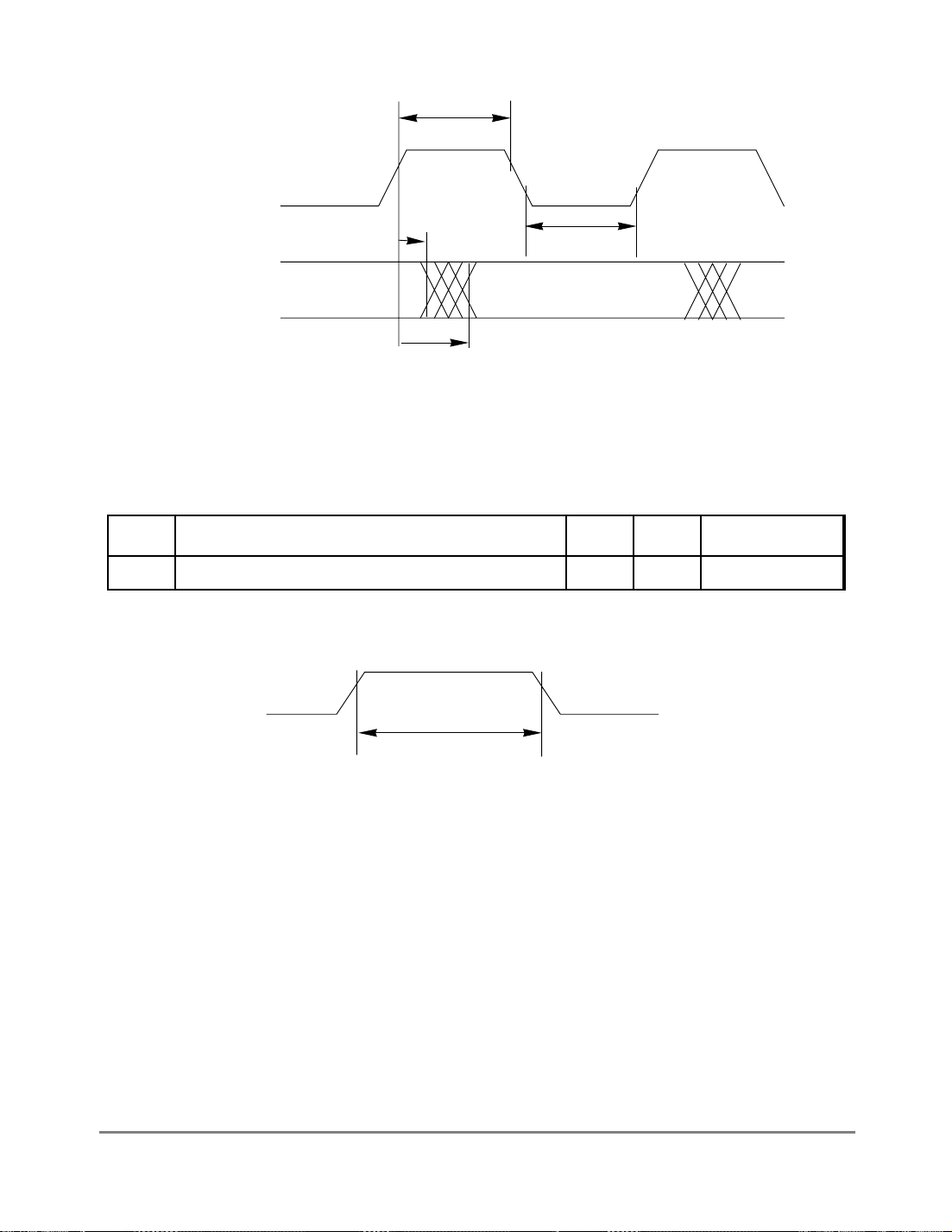
TX_CLK (input)
Fr
eescale S
emiconduct
or
, I
Freescale Semiconductor, Inc.
For More Information On This Product,
Go to: www.freescale.com
nc...
M7
M5
TXD[3:0] (outputs)
TX_EN
TX_ER
M6
M8
Figure 7-2. MII Transmit Signal Timing Diagram
7.3.3 MII Async Inputs Signal Timing (CRS, COL)
Table 7-3 provides information on the MII async inputs signal timing, shown in Figure 7-3.
Table 7-3. MII Async Inputs Signal Timing
Num Characteristic Min Max Unit
M9 CRS, COL minimum pulse width 1.5 Ñ TX_CLK period
Figure 7-3 shows the MII asynchronous inputs signal timing diagram.
CRS, COL
M9
Figure 7-3. MII Async Inputs Timing Diagram
MOTOROLA Chapter 7. Electrical Characteristics 7-3
PRELIMINARYÑSUBJECT TO CHANGE WITHOUT NOTICE
Page 64

Fr
eescale S
emiconduct
or
, I
Freescale Semiconductor, Inc.
For More Information On This Product,
Go to: www.freescale.com
nc...
7.3.4 MII Serial Management Channel Timing (MDIO,MDC)
Table 7-4 provides information on the MII serial management channel signal timing, shown
in Figure 7-4. The FEC functions correctly with a maximum MDC frequency in excess of
2.5 MHz. The exact upper bound is under investigation.
Table 7-4. MII Serial Management Channel Timing
Num Characteristic
M10 MDC falling edge to MDIO output invalid (minimum
propagation delay)
M11 MDC falling edge to MDIO output valid (max prop delay) Ñ 25
M12 MDIO (input) to MDC rising edge setup 10 Ñ ns
M13 MDIO (input) to MDC rising edge hold 0 Ñ
M14 MDC pulse width high 40% 60% MDC period
Min
(ns)
0Ñns
Max
(ns)
Unit
M15 MDC pulse width low 40% 60% MDC period
Figure 7-4 shows the MII serial management channel timing diagram.
M14
MM15
MDC (output)
M10
MDIO (output)
M11
MDIO (input)
M12
M13
Figure 7-4. MII Serial Management Channel Timing Diagram
7-4 MPC860T (Rev. D) Fast Ethernet Controller Supplement MOTOROLA
PRELIMINARYÑSUBJECT TO CHANGE WITHOUT NOTICE
Page 65

Fr
eescale S
emiconduct
or
, I
Freescale Semiconductor, Inc.
For More Information On This Product,
Go to: www.freescale.com
nc...
7.4 MPC860T Pin Assignments
Figure 7-5 shows the MPC860T pin assignments. Pins that support the FEC are shown in
black.
M_RxD0M_Rx_CLKM_TxD1M_Tx_CLK D 0 D4 D1 D2 D3 D5 VDDL D6 D7 D29 CLKOUT IPA3DP2
M_RxD1 M_Rx_DV IRQ0
M_RxD2
PB14 M_TxD2 IRQ1
PC5 M_Tx_ER VDDH D12 D17 D9 D15 D22 D25 D31 IPA6 IPA0 IPA7 XFCIPA1PC4 M_Rx_ER VDDSYNPA 1
PA2 MDC
PB17 VDDH GND R
PA5 PB16 TEXP EXTCLKHRESET
PB18 EXTALPB19
PC8 PC7
PA 7
PC10
PA 6
PC9 PB20 AS
PA9 PB21 GND IPB6 ALEABADDR30PB23 IRQ4
PB24 PB25 IPB1 IPB2IPB5PA10 ALEBPC11
M_MDIO TCK IRQ2 IPB0M_COLTDI IPB7VDDL
TMS PA11 IRQ6
PC12 VDDH
PC13 PB29
PC14 PC15 NC NC A15 A19 A25 A18 BSA0
PA15 A3 A12 A16 A20 A24 A26 TSIZ1 BSA1
A1 A6 A13 A17 A21 A23 A22 TSIZ0 BSA3
A2 A7 A14 A27 A29 A30 A28 A31 VDDL BSA2
18 16 141312111098765 32417 15 119
D13 D27 D10 D14 D18 D20 D24 D28 DP1 DP0 NCDP3M_TxD0 M_Tx_EN
D8 D23 D11 D16 D19 D21 D26 D30 IPA5 IPA2 NCIPA4M_RxD3 M_TxD3 VSSSYNPA0
VDDH
GND GND
VDDH VDDH
GPLA0 NC CS6 GPLA5 BDIPCS2PA14 A8 TEAPB28
WE0 GPLA1 GPLA3 CS0 TACS7PB31 A9 GPLA4PB30
M_CRS WE2 GPLA2 CE1A WRCS5A4 A10 GPLB4A0
WE1 WE3 CE2A CS1CS4A5 A11
Figure 7-5. MPC860T Pinout DiagramÑTop View
VDDH
W
KAPWRPC6
VDDL
V
U
T
R
P
N
M
L
K
J
VSSSYN1
W
AIT_APORESETWAIT_BPB15
STCONFSRESETVDDHPA3 GND XTALPA4
BADDR28BADDR29MODCK2
OP1OP0PA 8 MODCK1PB22
H
IPB4BRTDO IPB3TRESET
TS
IRQ3VDDHPA12 BURSTPB26
BI
BGCS3PA13 BBPB27
G
F
E
D
C
B
A
The following pins are marked as spare on the 860:
¥ B7: SPARE1/MII_CRS
¥ H18: SPARE2/MII_MDIO
¥ V15: SPARE3/MII_TX_EN
¥ H4: SPARE4/MII_COL
MOTOROLA Chapter 7. Electrical Characteristics 7-5
PRELIMINARYÑSUBJECT TO CHANGE WITHOUT NOTICE
Page 66

Fr
eescale S
emiconduct
or
, I
Freescale Semiconductor, Inc.
For More Information On This Product,
Go to: www.freescale.com
nc...
7-6 MPC860T (Rev. D) Fast Ethernet Controller Supplement MOTOROLA
PRELIMINARYÑSUBJECT TO CHANGE WITHOUT NOTICE
Page 67

Fr
eescale S
emiconduct
or
, I
Freescale Semiconductor, Inc.
For More Information On This Product,
Go to: www.freescale.com
nc...
MOTOROLA Chapter 7. Electrical Characteristics 7-7
PRELIMINARYÑSUBJECT TO CHANGE WITHOUT NOTICE
Page 68

Fr
eescale S
emiconduct
or
, I
Freescale Semiconductor, Inc.
For More Information On This Product,
Go to: www.freescale.com
nc...
 Loading...