

Page 1

Freescale Semiconductor
Document Number: MPC8360EEC
Technical Data
MPC8360E/MPC8358E
PowerQUICC II Pro Processor
Revision 2.x TBGA Silicon
Hardware Specifications
Rev. 4, 01/2011
This document provides an overview of the MPC8360E/58E
PowerQUICC II Pro processor revision 2.x TBGA features,
including a block diagram showing the major functional
components. This device is a cost-effective, highly
integrated communications processor that addresses the
needs of the networking, wireless infrastructure, and
telecommunications markets. Target applications include
next generation DSLAMs, network interface cards for 3G
base stations (Node Bs), routers, media gateways, and high
end IADs. The device extends current PowerQUICC II Pro
offerings, adding higher CPU performance, additional
functionality, faster interfaces, and robust interworking
between protocols while addressing the requirements related
to time-to-market, price, power, and package size. This
device can be used for the control plane and also has data
plane functionality.
For functional characteristics of the processor, refer to the
MPC8360E PowerQUICC II Pro Integrated
Communications Processor Family Reference Manual,
Rev. 3.
To locate any updates for this document, refer to the
MPC8360E product summary page on our website listed on
the back cover of this document or contact your Freescale
sales office.
Contents
1. Overview . . . . . . . . . . . . . . . . . . . . . . . . . . . . . . 2
2. Electrical Characteristics . . . . . . . . . . . . . . . . . . 8
3. Power Characteristics . . . . . . . . . . . . . . . . . . . 13
4. Clock Input Timing . . . . . . . . . . . . . . . . . . . . . 15
5. RESET Initialization . . . . . . . . . . . . . . . . . . . . 17
6. DDR and DDR2 SDRAM . . . . . . . . . . . . . . . . 20
7. DUART . . . . . . . . . . . . . . . . . . . . . . . . . . . . . . 27
8. UCC Eth er net Controller: Three-Speed Ethernet,
MII Management . . . . . . . . . . . . . . . . . . . . . . . 28
9. Local Bus . . . . . . . . . . . . . . . . . . . . . . . . . . . . . 41
10. JTAG . . . . . . . . . . . . . . . . . . . . . . . . . . . . . . . . 48
2
11. I
C . . . . . . . . . . . . . . . . . . . . . . . . . . . . . . . . . . 52
12. PCI . . . . . . . . . . . . . . . . . . . . . . . . . . . . . . . . . . 54
13. Timers . . . . . . . . . . . . . . . . . . . . . . . . . . . . . . . 56
14. GPIO . . . . . . . . . . . . . . . . . . . . . . . . . . . . . . . . 57
15. IPIC . . . . . . . . . . . . . . . . . . . . . . . . . . . . . . . . . 58
16. SPI . . . . . . . . . . . . . . . . . . . . . . . . . . . . . . . . . . 58
17. TDM/SI . . . . . . . . . . . . . . . . . . . . . . . . . . . . . . 60
18. UTOPIA/POS . . . . . . . . . . . . . . . . . . . . . . . . . 62
19. H D LC, BISYNC, Transparent, and Synchronous
UART . . . . . . . . . . . . . . . . . . . . . . . . . . . . . . . 64
20. USB . . . . . . . . . . . . . . . . . . . . . . . . . . . . . . . . . 67
21. Package and Pin Listings . . . . . . . . . . . . . . . . . 68
22. Clocking . . . . . . . . . . . . . . . . . . . . . . . . . . . . . 85
23. Thermal . . . . . . . . . . . . . . . . . . . . . . . . . . . . . . 97
24. System Design Information . . . . . . . . . . . . . . 102
25. Ordering Information . . . . . . . . . . . . . . . . . . . 106
26. Document Revision History . . . . . . . . . . . . . 107
© 2011 Freescale Semiconductor, Inc. All rights reserved.
Page 2

Overview
Memory Controllers
GPCM/UPM/SDRAM
32/64 DDR Interface Unit
PCI Bridge
Local Bus
Bus Arbitration
DUART
Dual I2C
4 Channel DMA
Interrupt Controller
Protection & Configuration
System Reset
Clock Synthesizer
System Interface Unit
(SIU)
Local
Baud Rate
Generators
Multi-User
RAM
UCC8
Parallel I/O
Accelerators
Dual 32-Bit RISC CP
Serial DMA
&
2 Virtual
DMAs
2 GMII/
RGMII/TBI/RTBI
8 MII/
RMII
8 TDM Ports
2 UTOPIA/POS
(124 MPHY)
Serial Interface
QUICC Engine Module
JTAG/COP
Power
Management
Timers
FPU
Classic G2 MMUs
32KB
D-Cache
32KB
I-Cache
Security Engine
e300 Core
PCI
DDRC1
UCC7
UCC6
UCC5
UCC4
UCC3
UCC2
UCC1
MCC
USB
SPI2
Time Slot Assigner
DDRC2
SPI1
1Overview
This section describes a high-level overview including features and general operation of the
MPC8360E/58E PowerQUICC II Pro processor. A major component of this device is the e300 core, which
includes 32 Kbytes of instruction and data cache and is fully compatible with the Power Architecture™
603e instruction set. The new QUICC Engine module provides termination, interworking, and switching
between a wide range of protocols including ATM, Ethernet, HDLC, and POS. The QUICC Engine
module’s enhanced interworking eases the transition and reduces investment costs from A TM to IP based
systems. The other major features include adual DDR SDRAM memory controller for the MPC8360E,
which allows equipment providers to partition system para me ters and data in an extr eme ly ef fic ie nt way,
such as using one 32-bit DDR memory controller for control plane processing and the other for data plane
processing. The MPC8358E has a single DDR SDRAM memory controller. The MPC8360E/58E also
offers a 32-bit PCI controller, a flexible local bus, and a dedicated security engine.
Figure 1 shows the MPC8360Eblock diagram.
MPC8360E/MPC8358E PowerQUICC II Pro Processor Revision 2.x TBGA Silicon Hardware Specifications, Rev. 4
2 Freescale Semiconductor
Figure 1. MPC8360E Block Diagram
Page 3

Figure 2 shows the MPC8358E block diagram.
Memory Controllers
GPCM/UPM/SDRAM
32/64 DDR Interface Unit
PCI Bridge
Local Bus
Bus Arbitration
DUART
Dual I2C
4 Channel DMA
Interrupt Controller
Protection & Configuration
System Reset
Clock Synthesizer
System Interface Unit
(SIU)
Local
Baud Rate
Generators
Multi-User
RAM
UCC8
Parallel I/O
Accelerators
Dual 32-Bit RISC CP
Serial DMA
&
2 Virtual
DMAs
2 GMII/
RGMII/TBI/RTBI
6 MII/
RMII
4 TDM Ports
1 UTOPIA/POS
(31/124 MPHY)
Serial Interface
QUICC Engine Module
JTAG/COP
Power
Management
Timers
FPU
Classic G2 MMUs
32KB
D-Cache
32KB
I-Cache
Security Engine
e300 Core
PCI
DDRC
UCC5
UCC4
UCC3
UCC2
UCC1
USB
SPI2
Time Slot Assigner
SPI1
Overview
Figure 2. MPC8358E Block Diagram
Major features of the MPC8360E/58E are as follows:
• e300 PowerPC processor core (enhanced version of the MPC603e core)
— Operates at up to 667 MHz (for the MPC8360E) and 400 MHz (for the MPC8358E)
— High-performance, superscalar processor core
— Floating-point, integer, load/store, system register, and branch processing units
— 32-Kbyte instruction cache, 32-Kbyte data cache
— Lockable portion of L1 cache
— Dynamic power management
— Software-compatible with the Freescale processor families implementing the Power
Architecture™ technology
• QUICC Engine unit
— Two 32-bit RISC controllers for flexible support of the communications peripherals, each
operating up to 500 M Hz (for the MPC8360E) and 400 MHz (for the MPC8358E)
— Serial DMA channel for receive and transmit on all serial channels
MPC8360E/MPC8358E PowerQUICC II Pro Processor Revision 2.x TBGA Silicon Hardware Specifications, Rev. 4
Freescale Semiconductor 3
Page 4

Overview
— QUICC Engine module peripheral request interface (for SEC, PCI, IEEE Std. 1588™)
— Eight universal communication controllers (UCCs) on the MPC8360E and six UCCs on the
MPC8358E supporting the following protocols and interfaces (not all of them simultaneous ly):
– IEEE 1588 protocol supported
– 10/100 Mbps Ethernet/IEEE Std. 802.3™ CDMA/CS interface through a
media-independent interface (MII, RMII, RGMII)
1
– 1000 Mbps Ethernet/IEEE 802.3 CDMA/CS interface through a media-independent
interfac e (GM II, RGMII, TBI, RTB I) on UCC1 and UCC2
– 9.6-Kbyte jumbo frames
– ATM full-duplex SAR, up to 622 Mbps (OC-12/STM-4), AAL0, AAL1, and AAL5 in
accordance ITU-T I.363.5
– AT M AAL2 CPS, SSSAR, and SSTED up to 155 Mbps (OC-3/STM-1) Mbps full duplex
(with 4 CPS packets per cell) in accordance ITU-T I.366.1 and I.363.2
– ATM traffic shaping for CBR, VBR, UBR, and GFR traffic types compatible with ATM
forum TM4.1 for up to 64-Kbyte simultaneous ATM channels
– ATM AAL1 structured and unstructured circuit emulation service (CES 2.0) in accordance
with ITU-T I.163.1 and ATM Forum af-vtoa-00-0078.000
– IMA (Inverse Multiplexing over ATM) for up to 31 IMA links over 8 IMA groups in
accordance with the ATM forum AF-PHY-0086.000 (Version 1.0) and AF-PHY-0086.001
(Version 1.1)
– AT M Transmission Convergence layer support in accordance with ITU-T I.432
– AT M OAM handling features compatible with ITU-T I.610
– PPP, Multi- Link (ML-PPP) , Multi-Class (MC-PPP ) and PPP mux in accordance with the
following RFCs: 1661, 1662, 1990, 2686, and 3153
– IP support for IPv4 packets including TOS, TTL, and header checksum processing
– Ethernet over first mile IEEE 802.3ah
– Shim header
– Ethernet-to-Ethernet/AAL5/AAL2 inter-working
– L2 Ethernet switching using MAC address or IEEE Std. 802.1P/Q™ VLAN tags
– ATM (AAL2/AAL5) to Ethernet (IP) interworking in accordance with RFC2684 including
bridging of ATM ports to Ethernet ports
– Extensive support for ATM statistics and Ethernet RMON/MIB statistics
– AAL2 protocol rate up to 4 CPS at OC-3/STM-1 rate
– Packet over Sonet (POS) up to 622-Mbps full-duplex 124 MultiPHY
– POS hardware; microcode must be loaded as an IRAM package
– Transparent up to 70-Mbps full-duplex
– HDLC up to 70-Mbps full-duplex
– HDLC BUS up to 10 Mbps
1.SMII or SGMII media-inde pendent interface is not currently supported.
MPC8360E/MPC8358E PowerQUICC II Pro Processor Revision 2.x TBGA Silicon Hardware Specifications, Rev. 4
4 Freescale Semiconductor
Page 5

Overview
– Asynchronous HDLC
– UART
– BISYNC up to 2 Mbps
– User-programmable Virtual FIFO size
– QUICC multichannel controller (QMC) for 64 TDM channels
— One multichannel communication controller (MCC) only on the MPC8360E supporting the
following:
– 256 HDLC or transparent channels
– 128 SS7 channels
– Almost any combination of subgroups can be multiplexed to single or multiple TDM
interfaces
— Two UTOPIA/POS interfaces on the MPC8360E supporting 124 MultiPHY each (optional
2*128 MultiPHY with extended address) and one UTOPIA/POS interface on the MPC8358E
supporting 31/124 MultiPHY
— Two serial pe rip he ra l in te rfaces (SPI); SPI2 is dedicated to Ethernet PHY management
— Eight TDM interfaces on the MPC8360E and four TDM interfaces on the MPC8358E with
1-bit mode for E3/T3 rates in clear channel
— Sixteen independent baud rate generators and 30 input clock pins for supplying clocks to UCC
and MCC serial channels (MCC is only available on the MPC8360E)
— Four independent 16-bit timers that can be interconnected as four 32-bit timers
— Interworking functionality:
– Layer 2 10/100-Base T Ethernet switch
– ATM-to-ATM switching (AAL0, 2, 5)
– Ethernet-to-ATM switching with L3/L4 support
– PPP interworking
• Security engine is optimized to handle all the algorithms asso ciated with IPS ec, SSL/TLS, SR TP,
802.11i®, iSCSI, and IKE processing. The security engine contains four crypto-channels, a
controller, and a set of crypto execution units (EUs).
— Public key execution unit (PKEU) supporting the following:
– RSA and Diffie-Hellman
– Programmable field size up to 2048 bits
– Elliptic curve cryptography
– F2m and F(p) modes
– Programmable field size up to 511 bits
— Data encryption standard execution unit (DEU)
–DES, 3DES
– Two key (K1, K2) or three key (K1, K2, K3)
– ECB and CBC modes for both DES and 3DES
— Advanced encryption standard unit (AESU)
MPC8360E/MPC8358E PowerQUICC II Pro Processor Revision 2.x TBGA Silicon Hardware Specifications, Rev. 4
Freescale Semiconductor 5
Page 6

Overview
— Implements the Rinjdael symmetric key cipher
— Key lengths of 128, 192, and 256 bits, two key
– ECB, CBC, CCM, and counter modes
— ARC four execution unit (AFEU)
– Implements a stream cipher compatible with the RC4 algorithm
– 40- to 128-bit programmable key
— Message digest execution unit (MDEU)
– SHA with 160-, 224-, or 256-bit message digest
– MD5 with 128-bit message digest
– HMAC with either SHA or MD5 algorithm
— Random number generator (RNG)
— Four crypto-channels, each supporting multi-command descriptor chains
– Static and/or dynamic assignment of crypto-execution units via an integrated controller
– Buffer size of 256 bytes for each execution unit, with flow control for large data sizes
— Storage/NAS XOR parity generation accelerator for RAID applications
• Dual DDR SDRAM memory controllers on the MPC8360E and a single DDR SDRAM memory
controller on the MPC8358E
— Programmable timing supporting both DDR1 and DDR2 SDRAM
— On the MPC8360E, the DDR buses can be configured as two 32-bit buses or one 64-bit bus;
on the MPC8358E, the DDR bus can be configured as a 32- or 64-bit bus
— 32- or 64-bit data interface, up to 333 MHz (for the MPC8360E) and 266 MHz (for the
MPC8358E) data rate
— Four banks of memory, each up to 1 Gbyte
— DRAM chip configurations from 64 Mbits to 1 Gigabit with ×8/×16 data ports
— Full ECC support (when the MPC8360E is configured as 2×32-bit DDR memory controllers,
both support ECC)
— Page mode support (up to 16 s imultaneous open pages for DDR1, up to 32 simultaneous open
pages for DDR2)
— Contiguous or discontiguous memory mapping
— Read-modify-write support
— Sleep mode support for self refresh SDRAM
— Supports auto refreshing
— Supports source clock mode
— On-the-fly power management using CKE
— Registered DIMM support
— 2.5-V SSTL2 compa tible I/O for DDR1, 1.8-V SST L2 c omp at ible I/ O for DDR2
— External driver impedance calibration
— On-die termination (ODT)
MPC8360E/MPC8358E PowerQUICC II Pro Processor Revision 2.x TBGA Silicon Hardware Specifications, Rev. 4
6 Freescale Semiconductor
Page 7

• PCI interface
— PCI Specification Revision 2.3 compatible
— Data bus widths:
– Single 32-bit data PCI interface that operates at up to 66 MHz
— PCI 3.3-V compatible (not 5-V compatible)
— PCI host bridge capabilities on both interfaces
— PCI agent mode supported on PCI interface
— Support for PCI-to-memory and memory-to-PCI streaming
— Memory prefetching of PCI read accesses and support for delayed read transactions
— Support for posting of processor-to-PCI and PCI-to-memory writes
— On-chip arbitration, supporting five masters on PCI
— Support for accesses to all PCI address spaces
— Parity support
— Selectable hardware-enforced coherency
— Address translation units for address mapping between host and peripheral
— Dual address cycle supported when the device is the target
Overview
— Internal configuration registers accessible from PCI
• Local bus controller (LBC)
— Multiplexed 32-bit address and data operating at up to 133 MHz
— Eight chip selects support eight external slaves
— Up to eight-beat burst transfers
— 32-, 16-, and 8-bit port sizes are controlled by an on-chip memory controller
— Three protocol engines available on a per chip select basis:
– General-purpose chip select machine (GPCM)
– Three user programmable machines (UPMs)
– Dedicated single data rate SDRAM controller
— Parity support
— Default boot ROM chip select with configurable bus width (8-, 16-, or 32-bit)
• Programmable interrupt controller (PIC)
— Functional and programming compatibility with the MPC8260 interrupt controller
— Support for 8 external and 35 internal discrete interrupt sources
— Support for one external (optional) and seven internal machine checkstop interrupt sources
— Programmable highest priority request
— Four groups of interrupts with programmable priority
— External and internal interrupts directed to communication proc ess o r
— Redirects interrupts to external INTA
— Unique vector number for each interrupt source
MPC8360E/MPC8358E PowerQUICC II Pro Processor Revision 2.x TBGA Silicon Hardware Specifications, Rev. 4
Freescale Semiconductor 7
pin when in core disable mode
Page 8

Electrical Characteristics
• Dual industry-standard I2C interfaces
— Two-wire interface
— Multiple master support
— Master or slave I2C mode support
— On-chip digital filtering rejects spikes on the bus
— System initialization data is optionally loaded from I
embedded hardware
• DMA controller
— Four independent virtual channels
— Concurrent execution across multiple channels with programmable bandwidth control
— All channels accessible by local core and remote PCI masters
— Misaligned transfer capability
— Data chaining and direct mode
— Interrupt on completed segment and chain
— DMA external handshake signals: DMA_DREQ[0:3]/DMA_DACK[0:3]/DMA_DONE[0:3].
There is one set for each DMA channel. The pins are multiplexed to the parallel IO pins with
other QE functions.
• DUART
2
C-1 EPROM by boot sequencer
— T wo 4-wire interfaces (RxD, TxD, RTS, CTS)
— Programming model compatible with the original 16450 UART and the PC16550D
• System timers
— Periodic interrupt timer
— Real-time clock
— Software watchdog timer
— Eight general-purpose timers
• IEEE Std. 1149.1™-compliant, JTAG boundary scan
• Integrated PCI bus and SDRAM clock generation
2 Electrical Characteristics
This section provides the AC and DC electrical specificati ons and thermal char act er isti cs f or the
MPC8360E/58E. The device is currently targeted to these specifications. Some of these specifications are
independent of the I/O cell, but are included for a more complete reference. These are not pur ely I/O buffer
design specifications.
MPC8360E/MPC8358E PowerQUICC II Pro Processor Revision 2.x TBGA Silicon Hardware Specifications, Rev. 4
8 Freescale Semiconductor
Page 9

2.1 Overall DC Electrical Characteristics
This section covers the ratings, conditions, and other characteristics.
2.1.1 Absolute Maximum Ratings
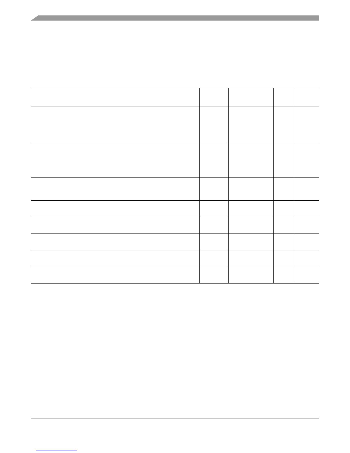
Table 1 provides the absolute maximum ratings.
Table 1. Absolute Maximum Ratings
Characteristic Symbol Max Value Unit Notes
Electrical Characteristics
1
Core supply voltage
V
For QUICC Engine module frequencies <500 MHz and e300
frequencies <667 MHz
For a QUICC Engine module frequency of 500 MHz or an e300
frequency of 667 MHz
PLL supply voltage
AV
For QUICC Engine module frequencies <500 MHz and e300
frequencies <667 MHz
For a QUICC Engine module frequency of 500 MHz or an e300
frequency of 667 MHz
DDR and DDR2 DRAM I/O voltage
GV
DDR
DDR2
Three-speed Ethernet I/O, MII management voltage LV
PCI, local bus, DUART, system control and power management, I
2
C,
OV
SPI, and JTAG I/O voltage
Input voltage DDR DRAM signals MV
DDR DRAM reference MV
Three-speed Ethernet signals LV
Local bus, DUART, CLKIN, system control
and power management, I
2
C, SPI, and
OV
JTAG signals
DD
DD
DD
DD
DD
REF
IN
V—
–0.3 to 1.32
–0.3 to 1.37
V—
–0.3 to 1.32
–0.3 to 1.37
V—
–0.3 to 2.75
–0.3 to 1.89
–0.3 to 3.63 V —
–0.3 to 3.63 V —
IN
–0.3 to (GVDD + 0.3) V 2, 5
–0.3 to (GVDD + 0.3) V 2, 5
–0.3 to (LVDD + 0.3) V 4, 5
IN
–0.3 to (OVDD + 0.3) V 3, 5
PCI OV
Storage temperature range T
Notes:
1. Functional and tested operating conditions are given in Ta bl e 2 . Absolute maximum ratings are stress ratings only, and
functional operation at the maximums is not guaranteed. Stresses beyond those listed may affect device reliability or cause
permanent damage to the device.
2. Caution: MV
must not exceed GVDD by more than 0.3 V. This limit may be exceeded for a maximum of 100 ms during
IN
power-on reset and power-down sequences.
3. Caution: OV
must not exceed OVDD by more than 0.3 V. This limit may be exceeded for a maximum of 100 ms during
IN
power-on reset and power-down sequences.
4. Caution: LV
must not exceed LVDD by more than 0.3 V. This limit may be exceeded for a maximum of 100 ms during
IN
power-on reset and power-down sequences.
5. (M,L,O)V
6. OV
on the PCI interface may overshoot/undershoot according to the PCI Electrical Specification for 3.3-V operation, as
IN
and MV
IN
may overshoot/undershoot to a voltage and for a maximum duration as shown in Figure 3.
REF
shown in Figure 4.
MPC8360E/MPC8358E PowerQUICC II Pro Processor Revision 2.x TBGA Silicon Hardware Specifications, Rev. 4
Freescale Semiconductor 9
IN
STG
–0.3 to (OVDD + 0.3) V 6
–55 to 150 °C—
Page 10
Electrical Characteristics
2.1.2 Power Supply Voltage Specification
Table 2 provides the recommended operating conditions for the device. Note that the values in Table 2 are
the recommended and tested operating conditions. Proper device operation outside of these conditions is
not guaranteed.
Table 2. Recommended Operating Conditions
Characteristic Symbol
Core supply voltage
For QUICC Engine module frequencies <500 MHz and e300
frequencies <667 MHz
For a QUICC Engine module frequency of 500 MHz or an e300
frequency of 667 MHz
PLL supply voltage
AV
For QUICC Engine module frequencies <500 MHz and e300
frequencies <667 MHz
For a QUICC Engine module frequency of 500 MHz or an e300
frequency of 667 MHz
DDR and DDR2 DRAM I/O supply voltage
GV
DDR
DDR2
Three-speed Ethernet I/O supply voltage LV
Three-speed Ethernet I/O supply voltage LV
Three-speed Ethernet I/O supply voltage LV
PCI, local bus, DUART, system control and power management, I
C, SPI,
OV
2
and JTAG I/O voltage
Recommended
Value
V
DD
1.2 V ± 60 mV
1.3 V ± 50 mV
DD
1.2 V ± 60 mV
1.3 V ± 50 mV
DD
2.5 V ± 125 mV
1.8 V ± 90 mV
0 3.3 V ± 330 mV
DD
2.5 V ± 125 mV
1 3.3 V ± 330 mV
DD
2.5 V ± 125 mV
2 3.3 V ± 330 mV
DD
2.5 V ± 125 mV
DD
3.3 V ± 330 mV V —
Unit Notes
V1
V1
V—
V—
V—
V—
Junction temperature T
J
0 to 105
°C2
–40 to 105
Notes:
1. GV
, LVDD, OVDD, AVDD, and VDD must track each other and must vary in the same direction—either in the positive or
DD
negative direction.
2. The operating conditions for junction temperature, T
0° to 70 °C. Refer to Errata General9 in
Chip Errata for the MPC8360E, Rev. 1
, on the 600/333/400 MHz and 500/333/500 MHz on rev. 2.0 silicon is
J
.
MPC8360E/MPC8358E PowerQUICC II Pro Processor Revision 2.x TBGA Silicon Hardware Specifications, Rev. 4
10 Freescale Semiconductor
Page 11

Figure 3 shows the undershoot and overshoot voltages at the interfaces of the device.
GND
GND – 0.3 V
GND – 0.7 V
Not to Exceed 10%
G/L/OVDD + 20%
G/L/OV
DD
G/L/OVDD + 5%
of t
interface
1
1. Note that t
interface
refers to the clock period associated with the bus clock interface.
V
IH
V
IL
Note:
Undervoltage
Waveform
Overvoltage
Waveform
11 ns
(Min)
+7.1 V
7.1 V p-to-p
(Min)
4 ns
(Max)
–3.5 V
7.1 V p-to-p
(Min)
62.5 ns
+3.6 V
0 V
4 ns
(Max)
Electrical Characteristics
Figure 3. Overshoot/Undershoot Voltage for GVDD/OVDD/LV
DD
Figure 4 shows the undershoot and overshoot voltage of the PCI interface of the device for the 3.3-V
signals, respectively.
Figure 4. Maximum AC Waveforms on PCI interface for 3.3-V Signaling
MPC8360E/MPC8358E PowerQUICC II Pro Processor Revision 2.x TBGA Silicon Hardware Specifications, Rev. 4
Freescale Semiconductor 11
Page 12
Electrical Characteristics
2.1.3 Output Driver Characteristics
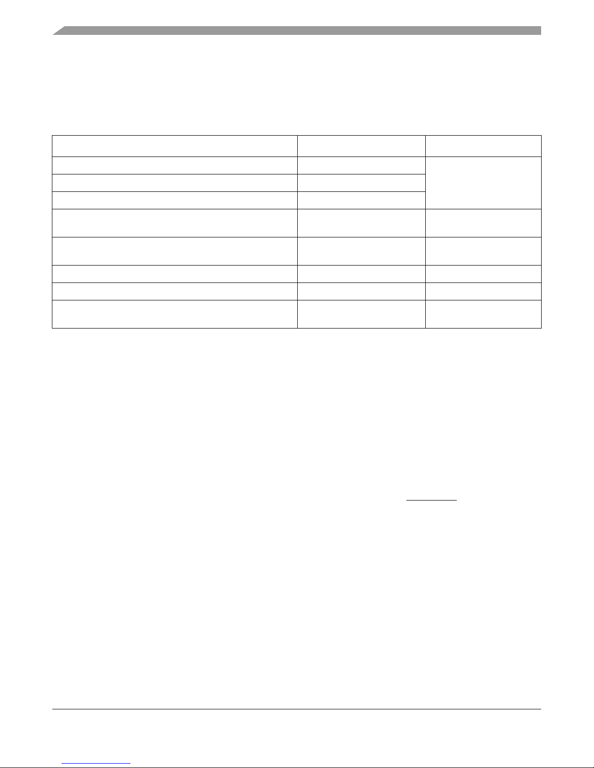
Table 3 provides information on the characteristics of the output driver strengths. The values are
preliminary estimates.
Table 3. Output Drive Capability
Driver Type Output Impedance (Ω) Supply Voltage
Local bus interface utilities signals 42 OV
PCI signals 25
PCI output clocks (including PCI_SYNC_OUT) 42
DDR signal 20
36 (half-strength mode)
DDR2 signal 18
36 (half-strength mode)
10/100/1000 Ethernet signals 42 LV
DUART, system control, I
GPIO signals 42 OV
1
DDR output impedance values for half strength mode are verified by design and not tested.
2
C, SPI, JTAG 42 OVDD = 3.3 V
1
1
= 3.3 V
DD
GV
= 2.5 V
DD
GVDD = 1.8 V
= 2.5/3.3 V
DD
= 3.3 V
DD
LV
= 2.5/3.3 V
DD
2.2 Power Sequencing
This section details the power sequencing considerations for the MPC8360E/58E.
2.2.1 Power-Up Sequencing
MPC8360E/58E does not require the core supply voltage (VDD and AVDD) and I/O supply voltages
(GVDD, LVDD, and OVDD) to be applied in any particular order. During the power ramp up, before the
power supplies are stable and if the I/O voltages are supplied before the core voltage, there may be a period
of time that all input and output pins will actively be driven and cause contention and excessive current.
In order to avoid actively driving the I/O pins and to eliminate excessive current draw, apply the core
voltage (V
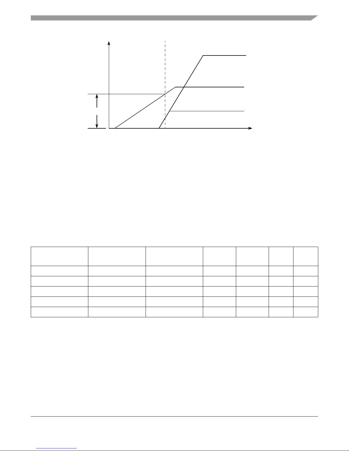
supplies fully ramp up. In the case where the core voltage is applied first, the core voltage supply must rise
to 90% of its nominal value before the I/O supplies reach 0.7 V, see Figure 5.
) before the I/O voltage (GVDD, LVDD, and OVDD) and assert PORESET before the power
DD
MPC8360E/MPC8358E PowerQUICC II Pro Processor Revision 2.x TBGA Silicon Hardware Specifications, Rev. 4
12 Freescale Semiconductor
Page 13
Power Characteristics
I/O Voltage (GVDD, LVDD, OVDD)
Core Voltage (V
DD
, AVDD)
90%
0.7 V
Time
Voltage
Figure 5. Power Sequencing Example
I/O voltage supplies (GVDD, L VDD, and OVDD) do not have any ordering require ments with res pect to one
another.
2.2.2 Power-Down Sequencing
The MPC8360E/58E does not requir e the core supply voltage and I/O supply voltages to be powered down
in any particular order.
3 Power Characteristics
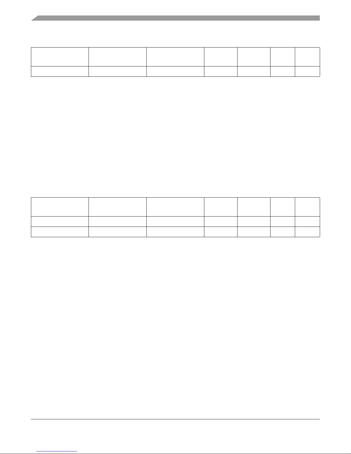
The estimated typical power dissipation values are shown in Table 4 and Table 5.
Table 4. MPC8360E TBGA Core Power Dissipation
Core
Frequency (MHz)
266 266 500 5.0 5.6 W 2, 3, 5
400 266 400 4.5 5.0 W 2, 3, 4
533 266 400 4.8 5.3 W 2, 3, 4
667 333 400 5.8 6.3 W 3, 6, 7, 8
500 333 500 5.9 6.4 W 3, 6, 7, 8
CSB
Frequency (MHz)
QUICC Engine
Frequency (MHz)
Typical Maximum Unit Notes
1
MPC8360E/MPC8358E PowerQUICC II Pro Processor Revision 2.x TBGA Silicon Hardware Specifications, Rev. 4
Freescale Semiconductor 13
Page 14
Power Characteristics
Table 4. MPC8360E TBGA Core Power Dissipation1 (continued)
Core
Frequency (MHz)
CSB
Frequency (MHz)
QUICC Engine
Frequency (MHz)
Typical Maximum Unit Notes
667 333 500 6.1 6.8 W 2, 3, 5, 9
Notes:
1. The values do not include I/O supply power (OV
2. Typical power is based on a voltage of V
= 1.2 V or 1.3 V, a junction temperature of TJ = 105°C, and a Dhrystone benchmark
DD
, LVDD, GVDD) or AVDD. For I/O power values, see Ta b l e 6 .
DD
application.
3. Thermal solutions will likely need to design to a value higher than typical power on the end application, T
power.
4. Maximum power is based on a voltage of V
5. Maximum power is based on a voltage of V
a junction T
= 105°C, and an artificial smoke test.
J
6. Typical power is based on a voltage of V
= 1.2 V, WC process, a junction TJ = 105°C, and an artificial smoke test.
DD
= 1.3 V for applications that use 667 MHz (CPU)/500 (QE) with WC process,
DD
= 1.3 V, a junction temperature of TJ = 70°C, and a Dhrystone benchmark
DD
application.
7. Maximum power is based on a voltage of V
a junction T
= 70°C, and an artificial smoke test.
J
= 1.3 V for applications that use 667 MHz (CPU) or 500 (QE) with WC process,
DD
8. This frequency combination is only available for rev. 2.0 silicon.
9. This frequency combination is not available for rev. 2.0 silicon.
1
Core
Frequency (MHz)
Table 5. MPC8358E TBGA Core Power Dissipation
CSB
Frequency (MHz)
QUICC Engine
Frequency (MHz)
Typical Maximum Unit Notes
target, and I/O
A
266 266 300 4.1 4.5 W 2, 3, 4
400 266 400 4.5 5.0 W 2, 3, 4
Notes:
1. The values do not include I/O supply power (OV
2. Typical power is based on a voltage of V
DD
, LVDD, GVDD) or AVDD. For I/O power values, see Ta b l e 6 .
DD
= 1.2 V, a junction temperature of TJ = 105°C, and a Dhrystone benchmark
application.
3. Thermal solutions will likely need to design to a value higher than typical power on the end application, T
power.
4. Maximum power is based on a voltage of V
= 1.2 V, WC process, a junction TJ = 105°C, and an artificial smoke test.
DD
target, and I/O
A
MPC8360E/MPC8358E PowerQUICC II Pro Processor Revision 2.x TBGA Silicon Hardware Specifications, Rev. 4
14 Freescale Semiconductor
Page 15

Table 6 shows the estimated typical I/O power dissipation for the device.
Table 6. Estimated Typical I/O Power Dissipation
Clock Input Timing
Interface Parameter
DDR I/O
65% utilization
R
= 20 Ω
s
R
= 50 Ω
t
2 pairs of clocks
Local Bus I/O
Load = 25 pf
3 pairs of clocks
PCI I/O
Load = 30 pF
200 MHz, 1 × 32 bits 0.3 0.46 — — — W —
200 MHz, 1 × 64 bits 0.4 0.58 — — — W —
200 MHz, 2 × 32 bits 0.6 0.92 — — — W —
266 MHz, 1 × 32 bits 0.35 0.56 — — — W —
266 MHz, 1 × 64 bits 0.46 0.7 — — — W —
266 MHz, 2 × 32 bits 0.7 1.11 — — — W —
333 MHz, 1 × 32 bits 0.4 0.65 — — — W —
333 MHz, 1 × 64 bits 0.53 0.82 — — — W —
333 MHz, 2 × 32 bits 0.81 1.3 — — — W —
133 MHz, 32 bits — — 0.22 — — W —
83 MHz, 32 bits — — 0.14 — — W —
66 MHz, 32 bits — — 0.12 — — W —
50 MHz, 32 bits — — 0.09 — — W —
33 MHz, 32 bits — — 0.05 — — W —
66 MHz, 32 bits — — 0.07 — — W —
GV
DD
(1.8 V)
GV
DD
(2.5 V)
OV
DD
(3.3 V)
LV
DD
(3.3 V)
LV
DD
(2.5 V)
Unit Comments
10/100/1000
Ethernet I/O
Load = 20 pF
Other I/O — — — 0.1 — — W —
MII or RMII — — — 0.01 — W Multiply by
GMII or TBI — — — 0.04 — W
RGMII or RTBI ————0.04W
number of
interfaces used.
4 Clock Input Timing
This section provides the clock input DC and AC electrical characteristics for the MPC8360E/58E.
NOTE
The rise/fall time on QUICC Engine block input pins should not exceed 5
ns. This should be enforced especially on clock signals. Rise time refers to
signal transitions from 10% to 90% of VDD; fall time refers to transitions
from 90% to 10% of V
DD
.
MPC8360E/MPC8358E PowerQUICC II Pro Processor Revision 2.x TBGA Silicon Hardware Specifications, Rev. 4
Freescale Semiconductor 15
Page 16

Clock Input Timing
4.1 DC Electrical Characteristics
Table 7 provides the clock input (CLKIN/PCI_SYNC_IN) DC timing specifications for the device.
Table 7. CLKIN DC Electrical Characteristics
Parameter Condition Symbol Min Max Unit
Input high voltage — V
Input low voltage — V
CLKIN input current 0 V ≤ V
PCI_SYNC_IN input current 0 V ≤ V
OV
– 0.5V ≤ VIN ≤ OV
DD
PCI_SYNC_IN input current 0.5 V ≤ V
≤ OV
IN
DD
≤ 0.5V or
IN
DD
≤ OVDD – 0.5 V I
IN
IH
IL
I
IN
I
IN
IN
2.7 OVDD + 0.3 V
–0.3 0.4 V
—±10μA
—±10μA
—±100μA
4.2 AC Electrical Characteristics
The primary clock source for the device can be one of two inputs, CLKIN or PCI_CLK, depending on
whether the device is configured in PCI host or PCI agent mode. Table 8 provides the clock input
(CLKIN/PCI_CLK) AC timing specifications for the device.
Table 8. CLKIN AC Timing Specifications
Parameter/Condition Symbol Min Typical Max Unit Notes
CLKIN/PCI_CLK frequency f
CLKIN/PCI_CLK cycle time t
CLKIN/PCI_CLK rise and fall time t
CLKIN/PCI_CLK duty cycle t
CLKIN
CLKIN
, t
KH
KL
KHK/tCLKIN
CLKIN/PCI_CLK jitter — — — ±150 ps 4, 5
— — 66.67 MHz 1
15 — — ns —
0.6 1.0 2.3 ns 2
40 — 60 % 3
Notes:
1. Caution: The system, core, USB, security, and 10/100/1000 Ethernet must not exceed their respective maximum or minimum
operating frequencies.
2. Rise and fall times for CLKIN/PCI_CLK are measured at 0.4 V and 2.7 V.
3. Timing is guaranteed by design and characterization.
4. This represents the total input jitter—short term and long term—and is guaranteed by design.
5. The CLKIN/PCI_CLK driver’s closed loop jitter bandwidth should be <500 kHz at –20 dB. The bandwidth must be set low to
allow cascade-connected PLL-based devices to track CLKIN drivers with the specified jitter.
MPC8360E/MPC8358E PowerQUICC II Pro Processor Revision 2.x TBGA Silicon Hardware Specifications, Rev. 4
16 Freescale Semiconductor
Page 17

4.3 Gigabit Reference Clock Input Timing
Table 9 provides the Gigabit reference clocks (GT X_CLK125) AC timing specifications.
Table 9. GTX_CLK125 AC Timing Specifications
At recommended operating conditions with LVDD = 2.5 ± 0.125 mV/ 3.3 V ± 165 mV
Parameter/Condition Symbol Min Typical Max Unit Notes
RESET Initialization
GTX_CLK125 frequency t
GTX_CLK125 cycle time t
GTX_CLK rise and fall time
LV
= 2.5 V
DD
LV
= 3.3 V
DD
GTX_CLK125 duty cycle
GMII & TBI
1000Base-T for RGMII & RTBI
GTX_CLK125 jitter — — — ±150 ps 2
Notes:
1. Rise and fall times for GTX_CLK125 are measured from 0.5 and 2.0 V for LV
LV
=3.3V.
DD
2. GTX_CLK125 is used to generate the GTX clock for the UCC Ethernet transmitter with 2% degradation. The GTX_CLK125
duty cycle can be loosened from 47%/53% as long as the PHY device can tolerate the duty cycle generated by GTX_CLK.
See Section 8.2.2, “MII AC Timing Specifications,” Section 8.2.3, “RMII AC Timing Specifications,” and Section 8.2.5, “RGMII
and RTBI AC Timing Specifications” for the duty cycle for 10Base-T and 100Base-T reference clock.
G125
G125
t
G125R/tG125F
t
G125H/tG125
— 125 — MHz —
—8—ns—
——
—
45
47
= 2.5 V and from 0.6 and 2.7 V for
DD
0.75
1.0
55
53
ns 1
%2
5 RESET Initialization
This section describes the DC and AC electrical specifications for the reset initialization timing and
electrical requirements of the MPC8360E/58E.
5.1 RESET DC Electrical Characteristics
Table 10 provides the DC electrical characteristics for the RESET pins of the device.
Table 10. RESET Pins DC Electrical Characteristics
Characteristic Symbol Condition Min Max Unit
Input high voltage V
Input low voltage V
Input current I
Output high voltage V
Output low voltage V
MPC8360E/MPC8358E PowerQUICC II Pro Processor Revision 2.x TBGA Silicon Hardware Specifications, Rev. 4
Freescale Semiconductor 17
IH
IL
IN
OH
OL
—2.0OV
— –0.3 0.8 V
——±10μA
I
= –8.0 mA 2.4 — V
OH
IOL = 8.0 mA — 0.5 V
+ 0.3 V
DD
Page 18

RESET Initialization
Table 10. RESET Pins DC Electrical Characteristics (continued)
Characteristic Symbol Condition Min Max Unit
Output low voltage V
OL
I
= 3.2 mA — 0.4 V
OL
Notes:
1. This table applies for pins PORESET
2. HRESET
and SRESET are open drain pins, thus VOH is not relevant for those pins.
, HRESET, SRESET, and QUIESCE.
5.2 RESET AC Electrical Characteristics
This section describes the AC electrical specifications for the reset initialization timing requireme nts of
the device. Table 11 provides the reset initialization AC timing specifications for the DDR SDRAM
component(s).
Table 11. RESET Initialization Timing Specifications
Parameter/Condition Min Max Unit Notes
Required assertion time of HRESET
Required assertion time of PORESET
or SRESET (input) to activate reset flow 32 — t
with stable clock applied to CLKIN
when the device is in PCI host mode
Required assertion time of PORESET
with stable clock applied to
PCI_SYNC_IN when the device is in PCI agent mode
HRESET
HRESET
/SRESET assertion (output) 512 — t
negation to SRESET negation (output) 16 — t
Input setup time for POR config signals (CFG_RESET_SOURCE[0:2] and
CFG_CLKIN_DIV) with respect to negation of PORESET
when the device is
in PCI host mode
PCI_SYNC_IN
32 — t
32 — t
4—t
CLKIN
PCI_SYNC_IN
PCI_SYNC_IN
PCI_SYNC_IN
CLKIN
1
2
1
1
1
2
Input setup time for POR config signals (CFG_RESET_SOURCE[0:2] and
CFG_CLKIN_DIV) with respect to negation of PORESET
when the device is
4—t
PCI_SYNC_IN
1
in PCI agent mode
Input hold time for POR config signals with respect to negation of HRESET
Time for the device to turn off POR config signals with respect to the
assertion of HRESET
Time for the device to turn on POR config signals with respect to the negation
of HRESET
0— ns
—4 ns 3
1—t
PCI_SYNC_IN
1, 3
Notes:
1. t
PCI_SYNC_IN
is the clock period of the input clock applied to PCI_SYNC_IN. When the device is In PCI host mode the primary
clock is applied to the CLKIN input, and PCI_SYNC_IN period depends on the value of CFG_CLKIN_DIV. See the
MPC8360E PowerQUICC II Pro Integrated Communications Processor Family Reference Manual
2. t
is the clock period of the input clock applied to CLKIN. It is only valid when the device is in PCI host mode. See the
CLKIN
MPC8360E PowerQUICC II Pro Integrated Communications Processor Family Reference Manual
for more details.
for more details.
3. POR config signals consists of CFG_RESET_SOURCE[0:2] and CFG_CLKIN_DIV.
MPC8360E/MPC8358E PowerQUICC II Pro Processor Revision 2.x TBGA Silicon Hardware Specifications, Rev. 4
18 Freescale Semiconductor
Page 19

RESET Initialization
Table 12 provides the PLL and DLL lock times.
Table 12. PLL and DLL Lock Times
Parameter/Condition Min Max Unit Notes
PLL lock times — 100 μs—
DLL lock times 7680 122,880 csb_clk cycles 1, 2
Notes:
1. DLL lock times are a function of the ratio between the output clock and the coherency system bus clock (csb_clk). A 2:1 ratio
results in the minimum and an 8:1 ratio results in the maximum.
2. The csb_clk is determined by the CLKIN and system PLL ratio. See Section 22, “Clocking,” for more information.
5.3 QUICC Engine Block Operating Frequency Limitations
This section specify the limits of the AC electrical characteristics for the opera tion of the QUICC Engine
block’s communication interfaces.
NOTE
The settings listed below are required for correct hardware interface
operation. Each protocol by itself requires a minimal QUICC Engine block
operating frequency setting for meeting the performance target. Because the
performance is a complex function of all the QUICC Engine block settings,
the user should make use of the QUICC Engine block performance utility
tool provided by Freescale to validate their system.
Table 13 lists the maximal QUICC Engine block I/O frequencies and the minimal QUICC Engine block
core frequency for each interface.
Table 13. QUICC Engine Block Operating Frequency Limitations
Interface
Ethernet Management: MDC/MDIO 10 (max) 10 20 —
MII 25 (typ) 100 50 —
RMII 50 (typ) 100 50 —
GMII/RGMII/TBI/RTBI 125 (typ) 1000 250 —
SPI (master/slave) 10 (max) 10 20 —
UCC through TDM 50 (max) 70 8 × F2
MCC 25 (max) 16.67 16 × F 2, 4
UTOPIA L2 50 (max) 800 2 × F2
POS-PHY L2 50 (max) 800 2 × F2
HDLC bus 10 (max) 10 20 —
HDLC/transparent 50 (max) 50 8/3 × F2, 3
Interface Operating
Frequency (MHz)
Max Interface Bit
Rate (Mbps)
Min QUICC Engine
Operating
Frequency
1
(MHz)
Notes
MPC8360E/MPC8358E PowerQUICC II Pro Processor Revision 2.x TBGA Silicon Hardware Specifications, Rev. 4
Freescale Semiconductor 19
Page 20

DDR and DDR2 SDRAM
Table 13. QUICC Engine Block Operating Frequency Limitations (continued)
Interface
Interface Operating
Frequency (MHz)
UART/async HDLC 3.68 (max internal ref
Max Interface Bit
Rate (Mbps)
115 (Kbps) 20 —
Min QUICC Engine
Operating
Frequency
1
(MHz)
Notes
clock)
BISYNC 2 (max) 2 20 —
USB 48 (ref clock) 12 96 —
Notes:
1. The QUICC Engine module needs to run at a frequency higher than or equal to what is listed in this table.
2. ‘F’ is the actual interface operating frequency.
3. The bit rate limit is independent of the data bus width (that is, the same for serial, nibble, or octal interfaces).
4. TDM in high-speed mode for serial data interface.
6 DDR and DDR2 SDRAM
This section describes the DC and AC electrical specifications for the DDR and DDR2 SDRAM interface
of the MPC8360E/58E.
6.1 DDR and DDR2 SDRAM DC Electrical Characteristics
Table 14 provides the recommended operating conditions for the DDR2 SDRAM component(s) of the
device when GVDD(typ) = 1.8 V.
Table 14. DDR2 SDRAM DC Electrical Characteristics for GVDD(typ) = 1.8 V
Parameter/Condition Symbol Min Max Unit Notes
I/O supply voltage GV
I/O reference voltage MV
I/O termination voltage V
Input high voltage V
Input low voltage V
Output leakage current I
Output high current (V
Output low current (V
MV
input leakage current I
REF
= 1.420 V) I
OUT
= 0.280 V) I
OUT
VREF
TT
IH
OZ
OH
OL
DD
REF
IL
1.71 1.89 V 1
0.49 × GV
MV
MV
REF
DD
– 0.04 MV
REF
+ 0.125 GV
–0.3 MV
0.51 × GV
REF
DD
+ 0.04 V 3
REF
+ 0.3 V —
DD
– 0.125 V —
V2
—±10μA4
–13.4 — mA —
13.4 — mA —
—±10μA—
MPC8360E/MPC8358E PowerQUICC II Pro Processor Revision 2.x TBGA Silicon Hardware Specifications, Rev. 4
20 Freescale Semiconductor
Page 21

DDR and DDR2 SDRAM
Table 14. DDR2 SDRAM DC Electrical Characteristics for GVDD(typ) = 1.8 V (continued)
Parameter/Condition Symbol Min Max Unit Notes
Input current (0 V ≤VIN ≤ OVDD)IIN—±10μA—
Notes:
1. GV
2. MV
3. V
is expected to be within 50 mV of the DRAM GV
DD
is expected to equal 0.5 × GVDD, and to track GVDD DC variations as measured at the receiver. Peak-to-peak noise
REF
on MV
TT
MV
cannot exceed ±2% of the DC value.
REF
is not applied directly to the device. It is the supply to which far end signal termination is made and is expected to equal
. This rail should track variations in the DC level of MV
REF
4. Output leakage is measured with all outputs disabled, 0 V
at all times.
DD
≤ V
REF
OUT
.
≤ GVDD.
Table 15 provides the DDR2 capacitance when GVDD(typ) = 1.8 V.
Table 15. DDR2 SDRAM Capacitance for GVDD(typ)=1.8 V
Parameter/Condition Symbol Min Max Unit Notes
Input/output capacitance: DQ, DQS, DQS
Delta input/output capacitance: DQ, DQS, DQS
C
IO
C
DIO
68pF1
—0.5pF1
Note:
1. This parameter is sampled. GV
= 1.8 V ± 0.090 V, f = 1 MHz, TA = 25°C, V
DD
= GVDD/2, V
OUT
(peak-to-peak) = 0.2 V.
OUT
Table 16 provides the recommended operating conditions for the DDR SDRAM component(s) of the
device when GVDD(typ) = 2.5 V.
Table 16. DDR SDRAM DC Electrical Characteristics for GVDD(typ) = 2.5 V
Parameter/Condition Symbol Min Max Unit Notes
I/O supply voltage GV
I/O reference voltage MV
I/O termination voltage V
Input high voltage V
Input low voltage V
Output leakage current I
Output high current (V
Output low current (V
MV
input leakage current I
REF
Input current (0 V ≤V
= 1.95 V) I
OUT
= 0.35 V) I
OUT
≤ OVDD)I
IN
DD
REF
TT
IH
IL
OZ
OH
OL
VREF
IN
Notes:
1. GV
2. MV
3. V
is expected to be within 50 mV of the DRAM GV
DD
is expected to be equal to 0.5 × GVDD, and to track GVDD DC variations as measured at the receiver. Peak-to-peak
REF
noise on MV
is not applied directly to the device. It is the supply to which far end signal termination is made and is expected to be
TT
equal to MV
may not exceed ±2% of the DC value.
REF
. This rail should track variations in the DC level of MV
REF
4. Output leakage is measured with all outputs disabled, 0 V
at all times.
DD
≤ V
OUT
2.375 2.625 V 1
0.49 × GV
MV
– 0.04 MV
REF
MV
+ 0.18 GV
REF
–0.3 MV
DD
0.51 × GV
DD
+ 0.04 V 3
REF
+ 0.3 V —
DD
– 0.18 V —
REF
—±10μA4
–15.2 — mA —
15.2 — mA —
—±10μA—
—±10μA—
.
REF
≤ GVDD.
V2
MPC8360E/MPC8358E PowerQUICC II Pro Processor Revision 2.x TBGA Silicon Hardware Specifications, Rev. 4
Freescale Semiconductor 21
Page 22

DDR and DDR2 SDRAM
Table 17 provides the DDR capacitance when GVDD(typ) = 2.5 V.
Table 17. DDR SDRAM Capacitance for GVDD(typ) = 2.5 V
Parameter/Condition Symbol Min Max Unit Notes
Input/output capacitance: DQ, DQS C
Delta input/output capacitance: DQ, DQS C
Note:
1. This parameter is sampled. GV
= 2.5 V ± 0.125 V, f = 1 MHz, TA = 25°C, V
DD
IO
DIO
68pF1
—0.5pF1
= GVDD/2, V
OUT
(peak-to-peak) = 0.2 V.
OUT
6.2 DDR and DDR2 SDRAM AC Electrical Characteristics
This section provides the AC electrical characteristics for the DDR and DDR2 SDRAM interface.
6.2.1 DDR and DDR2 SDRAM Input AC Timing Specifications
Table 18 provides the input AC timing specifications for the DDR2 SDRAM interface when
GVDD(typ) = 1.8 V.
Table 18. DDR2 SDRAM Input AC Timing Specifications for GVDD(typ) = 1.8 V
At recommended operating conditions with GVDD of 1.8 V ± 5%.
Parameter Symbol Min Max Unit Notes
AC input low voltage V
AC input high voltage V
IL
IH
Table 19 provides the input AC timing specifications for the DDR SDRAM interface when
GVDD(typ) = 2.5 V.
—MV
MV
+ 0.25 — V —
REF
– 0.25 V —
REF
Table 19. DDR SDRAM Input AC Timing Specifications
At recommended operating conditions with GVDD of 2.5 V ± 5%.
Parameter Symbol Min Max Unit Notes
AC input low voltage V
AC input high voltage V
Note:
1. Maximum possible skew between a data strobe (MDQS[n]) and any corresponding bit of data (MDQ[8n + {0...7}] if 0 ≤ n ≤ 7)
or ECC (MECC[{0...7}] if n = 8).
MPC8360E/MPC8358E PowerQUICC II Pro Processor Revision 2.x TBGA Silicon Hardware Specifications, Rev. 4
22 Freescale Semiconductor
IL
IH
—MV
MV
+ 0.31 — V —
REF
– 0.31 V —
REF
Page 23

Table 20. DDR and DDR2 SDRAM Input AC Timing Specifications Mode
MCK[n]
MCK[n]
t
MCK
MDQ[x]
MDQS[n]
t
DISKEW
D1D0
t
DISKEW
At recommended operating conditions with GVDD of (1.8 or 2.5 V) ± 5%.
Parameter Symbol Min Max Unit Notes
DDR and DDR2 SDRAM
MDQS—MDQ/MECC input skew per byte
333 MHz
266 MHz
200 MHz
Notes:
1. AC timing values are based on the DDR data rate, which is twice the DDR memory bus frequency.
2. Maximum possible skew between a data strobe (MDQS[n]) and any corresponding bit of data (MDQ[8n + {0...7}] if 0 ≤ n ≤ 7)
or ECC (MECC[{0...7}] if n = 8).
t
DISKEW
–750
–1125
–1250
750
1125
1250
ps 1, 2
Figure 6 shows the input timing diagram for the DDR controller.
Figure 6. DDR Input Timing Diagram
6.2.2 DDR and DDR2 SDRAM Output AC Timing Specifications
Table 21 and Table 22 provide the output AC timing specifications and measurement conditions for the
DDR and DDR2 SDRAM interface.
Table 21. DDR and DDR2 SDRAM Output AC Timing Specifications for Source
Synchronous Mode
At recommended operating conditions with GVDD of (1.8 V or 2.5 V) ± 5%.
Parameter
MCK[n] cycle time, (MCK[n]/MCK
Skew between any MCK to ADDR/CMD
MPC8360E/MPC8358E PowerQUICC II Pro Processor Revision 2.x TBGA Silicon Hardware Specifications, Rev. 4
Freescale Semiconductor 23
8
[n] crossing) t
333 MHz
266 MHz
200 MHz
Symbol
t
MCK
AOSKEW
1
Min Max Unit Notes
610ns2
ns 3
–1.0
–1.1
–1.2
0.2
0.3
0.4
Page 24

DDR and DDR2 SDRAM
Table 21. DDR and DDR2 SDRAM Output AC Timing Specifications for Source
Synchronous Mode (continued)
At recommended operating conditions with GVDD of (1.8 V or 2.5 V) ± 5%.
Parameter
8
ADDR/CMD output setup with respect to MCK
333 MHz
266 MHz
200 MHz
ADDR/CMD output hold with respect to MCK
333 MHz
266 MHz—DDR1
266 MHz—DDR2
200 MHz
MCS
(n) output setup with respect to MCK
333 MHz
266 MHz
200 MHz
MCS
(n) output hold with respect to MCK
333 MHz
266 MHz
200 MHz
MCK to MDQS t
MDQ/MECC/MDM output setup with respect to MDQS
333 MHz
266 MHz
200 MHz
MDQ/MECC/MDM output hold with respect to MDQS
333 MHz
266 MHz
200 MHz
Symbol
t
DDKHAS
t
DDKHAX
t
DDKHCS
t
DDKHCX
DDKHMH
t
DDKHDS
t
DDKLDS
t
DDKHDX
t
DDKLDX
1
Min Max Unit Notes
—ns4
2.1
2.8
3.5
—ns4
2.0
2.7
2.8
3.5
—ns4
2.1
2.8
3.5
—ns4
2.0
2.7
3.5
–0.8 0.7 ns 5, 9
,
—ns6
0.7
1.0
1.2
,
—ns6
0.7
1.0
1.2
MDQS preamble start t
DDKHMP
–0.5 × t
– 0.6 –0.5 × t
MCK
+ 0.6 ns 7
MCK
MPC8360E/MPC8358E PowerQUICC II Pro Processor Revision 2.x TBGA Silicon Hardware Specifications, Rev. 4
24 Freescale Semiconductor
Page 25

Table 21. DDR and DDR2 SDRAM Output AC Timing Specifications for Source
Synchronous Mode (continued)
At recommended operating conditions with GVDD of (1.8 V or 2.5 V) ± 5%.
DDR and DDR2 SDRAM
Parameter
8
MDQS epilogue end t
Symbol
DDKHME
1
Min Max Unit Notes
–0.6 0.9 ns 7
Notes:
1. The symbols used for timing specifications follow the pattern of t
inputs and t
(first two letters of functional block)(reference)(state)(signal)(state)
(first two letters of functional block)(signal)(state)(reference)(state)
for outputs. Output hold time can be read as DDR timing
for
(DD) from the rising or falling edge of the reference clock (KH or KL) until the output went invalid (AX or DX). For example,
t
(A) are setup (S) or output valid time. Also, t
symbolizes DDR timing (DD) for the time t
DDKHAS
memory clock reference (K) goes from the high (H) state until outputs
MCK
symbolizes DDR timing (DD) for the time t
DDKLDX
memory clock reference
MCK
(K) goes low (L) until data outputs (D) are invalid (X) or data output hold time.
2. All MCK/MCK
3. In the source synchronous mode, MCK/MCK
For the skew measurements referenced for t
referenced measurements are made from the crossing of the two signals ±0.1 V.
can be shifted in ¼ applied cycle increments through the clock control register.
AOSKEW
it is assumed that the clock adjustment is set to align the
address/command valid with the rising edge of MCK.
4. ADDR/CMD includes all DDR SDRAM output signals except MCK/MCK
, MCS, and MDQ/MECC/MDM/MDQS. For the
ADDR/CMD setup and hold specifications, it is assumed that the clock control register is set to adjust the memory clocks by
½ applied cycle.
5. Note that t
DDKHMH
from the rising edge of the MCK(n) clock (KH) until the MDQS signal is valid (MH). t
follows the symbol conventions described in note 1. For example, t
DDKHMH
DDKHMH
describes the DDR timing (DD)
can be modified through control
of the DQSS override bits in the TIMING_CFG_2 register. In source synchronous mode, this will typically be set to the same
delay as the clock adjust in the CLK_CNTL register. The timing parameters listed in the table assume that these two
parameters have been set to the same adjustment value. See the
Communications Processor Family Reference Manual
for a description and understanding of the timing modifications
MPC8360E PowerQUICC II Pro Integrated
enabled by use of these bits.
6. Determined by maximum possible skew between a data strobe (MDQS) and any corresponding bit of data (MDQ), ECC
(MECC), or data mask (MDM). The data strobe should be centered inside of the data eye at the pins of the device.
7. All outputs are referenced to the rising edge of MCK(n) at the pins of the device. Note that t
DDKHMP
follows the symbol
conventions described in note 1.
8. AC timing values are based on the DDR data rate, which is twice the DDR memory bus frequency.
9. In rev. 2.0 silicon, t
DDKHMH
–0.9 ns. Refer to Errata DDR18 in
maximum meets the specification of 0.6 ns. In rev. 2.0 silicon, due to errata, t
Chip Errata for the MPC8360E, Rev. 1
.
DDKHMH
minimum is
MPC8360E/MPC8358E PowerQUICC II Pro Processor Revision 2.x TBGA Silicon Hardware Specifications, Rev. 4
Freescale Semiconductor 25
Page 26
DDR and DDR2 SDRAM
ADDR/CMD
MCK[n]
MCK[n]
t
MCK
CMD NOOP
t
AOSKEW(min)
ADDR/CMD
CMD NOOP
t
AOSKEW(max)
Output
Z0 = 50 Ω
GVDD/2
R
L
= 50 Ω
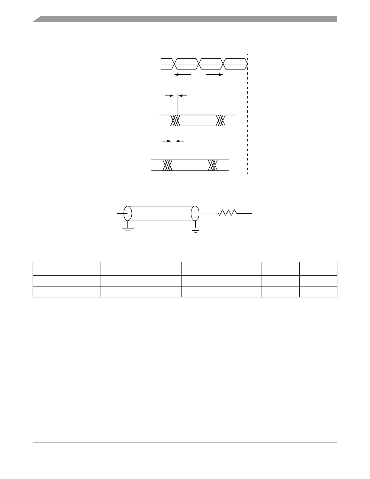
Figure 7 shows the DDR SDRAM output timing for address skew with respect to any MCK.
Figure 7. Timing Diagram for t
Figure 8 provides the AC test load for the DDR bus.
Figure 8. DDR AC Test Load
Table 22. DDR and DDR2 SDRAM Measurement Conditions
Symbol DDR DDR2 Unit Notes
V
TH
V
OUT
Notes:
1. Data input threshold measurement point.
2. Data output measurement point.
MV
± 0.31 V MV
REF
0.5 × GV
DD
AOSKEW
REF
0.5 × GV
Measurement
± 0.25 V V 1
DD
V2
MPC8360E/MPC8358E PowerQUICC II Pro Processor Revision 2.x TBGA Silicon Hardware Specifications, Rev. 4
26 Freescale Semiconductor
Page 27

Figure 9 shows the DDR SDRAM output timing diagram for source synchronous mode.
ADDR/CMD
t
DDKHAS
, t
DDKHCS
t
DDKHMH
t
DDKLDS
t
DDKHDS
MDQ[x]
MDQS[n]
MCK
[n]
MCK[n]
t
MCK
t
DDKLDX
t
DDKHDX
D1D0
Write A0 NOOP
t
DDKHME
t
DDKHMP
t
DDKHAX
, t
DDKHCX
DUART
Figure 9. DDR SDRAM Output Timing Diagram for Source Synchronous Mode
7DUART
This section describes the DC and AC electrical specifications for the DUART interface of the
MPC8360E/58E.
7.1 DUART DC Electrical Characteristics
Table 23 provides the DC electrical characteristics for the DUART interface of the device.
Table 23. DUART DC Electrical Characteristics
Parameter Symbol Min Max Unit Notes
High-level input voltage V
Low-level input voltage OV
High-level output voltage, I
Low-level output voltage, I
Input current (0 V ≤V
Note:
1. Note that the symbol V
DD
= –100 μAV
OH
= 100 μAV
OL
≤ OVDD)I
IN
, in this case, represents the OVIN symbol referenced in Ta bl e 1 and Ta b le 2 .
IN
IH
V
IL
OH
OL
IN
2OV
+ 0.3 V —
DD
–0.3 0.8 V —
OVDD – 0.4 — V —
—0.2V—
—±10μA1
MPC8360E/MPC8358E PowerQUICC II Pro Processor Revision 2.x TBGA Silicon Hardware Specifications, Rev. 4
Freescale Semiconductor 27
Page 28
UCC Ethernet Controller: Three-Speed Ethernet, MII Management
7.2 DUART AC Electrical Specifications
Table 24 provides the AC timing parameters for the DUART interface of the device.
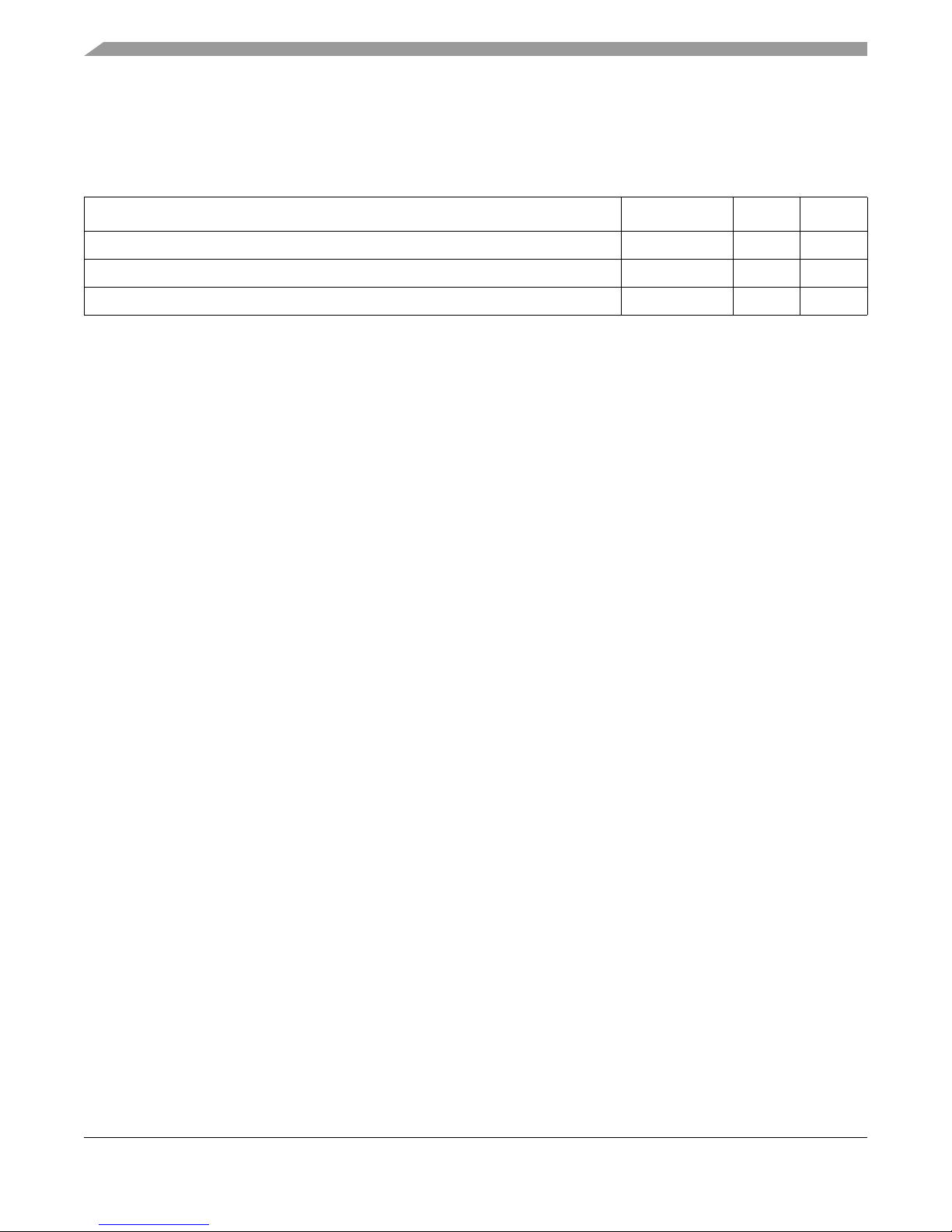
Table 24. DUART AC Timing Specifications
Parameter Value Unit Notes
Minimum baud rate 256 baud —
Maximum baud rate >1,000,000 baud 1
Oversample rate 16 — 2
Notes:
1. Actual attainable baud rate will be limited by the latency of interrupt processing.
2. The middle of a start bit is detected as the eighth sampled 0 after the 1-to-0 transition of the start bit. Subsequent bit values
are sampled each sixteenth sample.
8 UCC Ethernet Controller: Three-Speed Ethernet,
MII Management
This section provides the AC and DC electrical chara cteristics for three-speed, 10/100/1000, and MII
management.
8.1 Three-Speed Ethernet Controller (10/100/1000 Mbps)—
GMII/MII/RMII/TBI/RGMII/RTBI Electrical Characteristics
The electrical characteristics specified here apply to all GMII (gigabit media independent interface), MII
(media independent interface), RMII (reduced media independent interface), TBI (ten-bit interface) ,
RGMII (reduced gigabit media independent interface), and RTBI (reduced ten-bit interface) signals except
MDIO (management data input/output) and MDC (management data clock). The MII, RMII, GMII, and
TBI interfaces are only defined for 3.3 V, while the RGMII and RTBI interfaces are only defined for 2.5 V.
The RGMII and RTBI interfaces follow the Hewlett-Packard reduced pin-count interface for Gigabit
Ethernet Physical Layer Device Specification V ersion 1.2a (9/22/2000). The electrical characteristics for
the MDIO and MDC are specified in Section 8.3, “Ethernet Management Interface Electrical
Characteristics.”
8.1.1 10/100/1000 Ethernet DC Electrical Characteristics
The electrical characteristics specified here apply to media independent interface (MII), reduced gigabit
media independent interface (RGMII), reduced ten-bit interface (RTBI), reduced media independent
interface (RMII) signals, management data input/output (MDIO) and management data clock (MDC).
The MII and RMII interfaces are defined for 3.3 V , while the RGMII and R T BI interfaces can be operated
at 2.5 V. The RGMII and RTBI interfaces follow the Reduced Gigabit Media-Independent Interface
(RGMII) Specification Version 1.3. The RMII interface follo ws the RMII Consortium RMII Specification
Ver sion 1.2.
MPC8360E/MPC8358E PowerQUICC II Pro Processor Revision 2.x TBGA Silicon Hardware Specifications, Rev. 4
28 Freescale Semiconductor
Page 29
UCC Ethernet Controller: Three-Speed Ethernet, MII Management
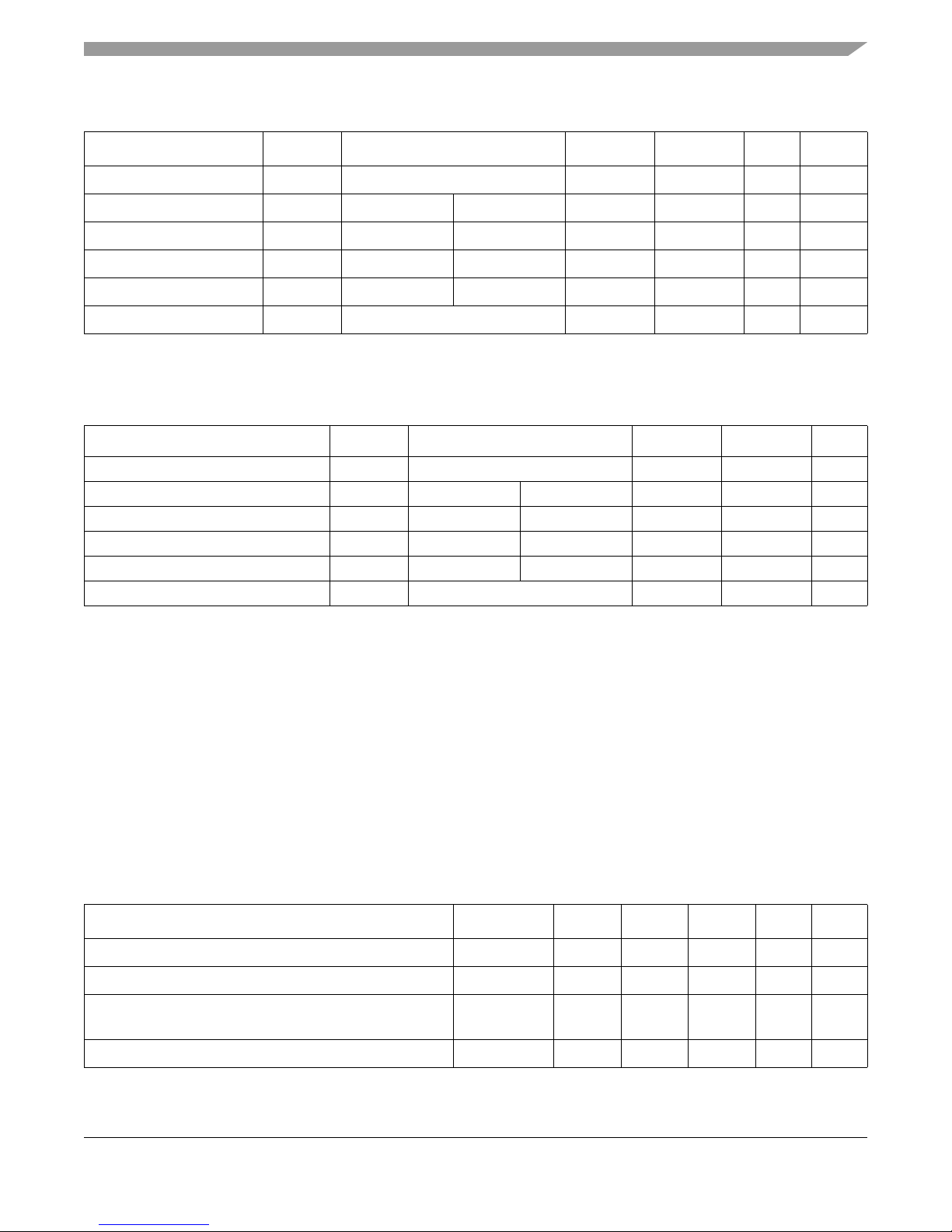
Table 25. RGMII/RTBI, GMII, TBI, MII, and RMII DC Electrical Characteristics (when operating at 3.3 V)
Parameter Symbol Conditions Min Max Unit Notes
Supply voltage 3.3 V LV
Output high voltage V
Output low voltage V
Input high voltage V
Input low voltage V
Input current I
DD
OH
OL
IH
IN
IOH = –4.0 mA LVDD = Min 2.40 LVDD + 0.3 V —
IOL = 4.0 mA LVDD = Min GND 0.50 V —
——2.0LV
IL
— — –0.3 0.90 V —
— 2.97 3.63 V 1
0 V ≤ VIN ≤ LV
DD
—±10μA—
Note:
1. GMII/MII pins that are not needed for RGMII, RMII, or RTBI operation are powered by the OV
Table 26. RGMII/RTBI DC Electrical Characteristics (when operating at 2.5 V)
Parameters Symbol Conditions Min Max Unit
Supply voltage 2.5 V LV
Output high voltage V
Output low voltage V
Input high voltage V
Input low voltage V
Input current I
DD
OH
OL
IH
IL
IN
IOH = –1.0 mA LVDD = Min 2.00 LVDD + 0.3 V
I
= 1.0 mA LV
OL
—LV
—LV
— 2.37 2.63 V
= Min GND – 0.3 0.40 V
DD
= Min 1.7 LVDD + 0.3 V
DD
= Min –0.3 0.70 V
DD
0 V ≤ VIN ≤ LV
DD
+ 0.3 V —
DD
supply.
DD
—±10μA
8.2 GMII, MII, RMII, TBI, RGMII, and RTBI AC Timing Specifications
The AC timing specifications for GMII, MII, TBI, RGMII, and RTBI are presented in this section.
8.2.1 GMII Timing Specifications
This sections describe the GMII transmit and receive AC timing specifications.
8.2.1.1 GMII Transmit AC Timing Specifications
Table 27 provides the GMII transmit AC timing specifications.
Table 27. GMII Transmit AC Timing Specifications
At recommended operating conditions with LVDD/OV
Parameter/Condition Symbol
GTX_CLK clock period t
GTX_CLK duty cycle t
GTX_CLK to GMII data TXD[7:0], TX_ER, TX_EN delay t
GTX_CLK clock rise time, (20% to 80%) t
of 3.3 V ± 10%.
DD
GTX
GTXH/tGTX
GTKHDX
t
GTKHDV
GTXR
1
Min Typ Max Unit Notes
—8.0—ns—
40 — 60 % —
0.5
—
——
5.0
ns 3
——1.0ns—
MPC8360E/MPC8358E PowerQUICC II Pro Processor Revision 2.x TBGA Silicon Hardware Specifications, Rev. 4
Freescale Semiconductor 29
Page 30
UCC Ethernet Controller: Three-Speed Ethernet, MII Management
GTX_CLK
TXD[7:0]
t
GTKHDX
t
GTX
t
GTXH
t
GTXR
t
GTXF
TX_EN
TX_ER
Table 27. GMII Transmit AC Timing Specifications (continued)
At recommended operating conditions with LVDD/OV
Parameter/Condition Symbol
of 3.3 V ± 10%.
DD
1
Min Typ Max Unit Notes
GTX_CLK clock fall time, (80% to 20%) t
GTX_CLK125 clock period t
GTX_CLK125 reference clock duty cycle measured at
LV
DD/2
t
G125H/tG125
GTXF
G125
——1.0ns—
—8.0—ns2
45 — 55 % 2
Notes:
1. The symbols used for timing specifications follow the pattern t
and t
(first two letters of functional block)(reference)(state)(signal)(state)
(GT) with respect to the t
clock reference (K) going to the high state (H) relative to the time date input signals (D) reaching
GTX
the valid state (V) to state or setup time. Also, t
GTKHDX
for outputs. For example, t
symbolizes GMII transmit timing (GT) with respect to the t
(first two letters of functional block)(signal)(state)(reference)(state)
symbolizes GMII transmit timing
GTKHDV
for inputs
GTX
reference (K) going to the high state (H) relative to the time date input signals (D) going invalid (X) or hold time. Note that, in
general, the clock reference symbol representation is based on three letters representing the clock of a particular functional.
For example, the subscript of t
represents the GMII(G) transmit (TX) clock. For rise and fall times, the latter convention is
GTX
used with the appropriate letter: R (rise) or F (fall).
2. This symbol is used to represent the external GTX_CLK125 signal and does not follow the original symbol naming
convention.
3. In rev. 2.0 silicon, due to errata, t
Refer to Errata
QE_ENET18
in
minimum and t
GTKHDX
GTKHDV
Chip Errata for the MPC8360E, Rev. 1
maximum are not supported when the GTX_CLK is selected.
.
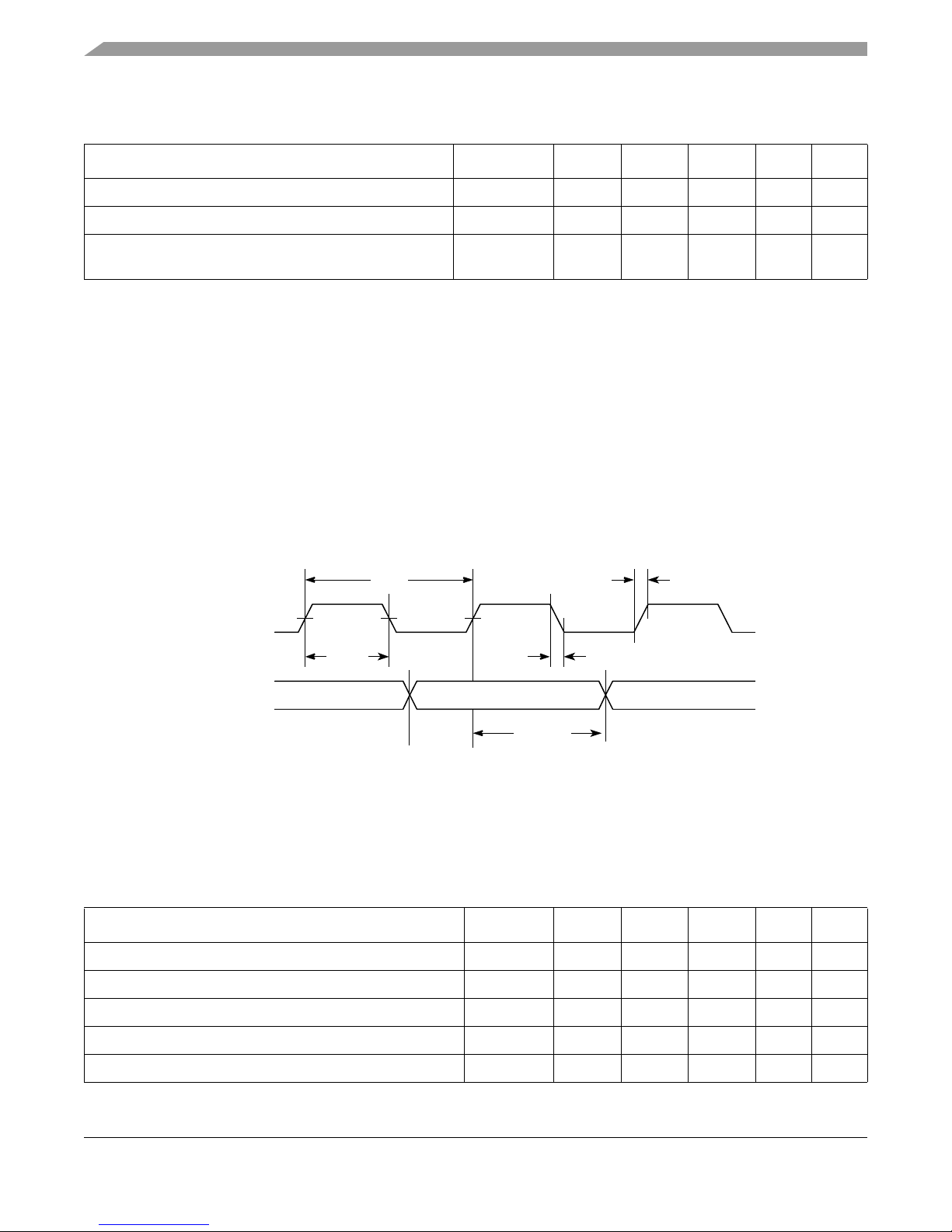
Figure 10 shows the GMII transmit AC timing diagram.
clock
Figure 10. GMII Transmit AC Timing Diagram
8.2.1.2 GMII Receive AC Timing Specifications
Table 28 provides the GMII receive AC timing specifications.
Table 28. GMII Receive AC Timing Specifications
At recommended operating conditions with LVDD/OV
Parameter/Condition Symbol
RX_CLK clock period t
RX_CLK duty cycle t
RXD[7:0], RX_DV, RX_ER setup time to RX_CLK t
RXD[7:0], RX_DV, RX_ER hold time to RX_CLK t
RX_CLK clock rise time, (20% to 80%) t
MPC8360E/MPC8358E PowerQUICC II Pro Processor Revision 2.x TBGA Silicon Hardware Specifications, Rev. 4
30 Freescale Semiconductor
of 3.3 V ± 10%.
DD
GRX
GRXH/tGRX
GRDVKH
GRDXKH
GRXR
1
Min Typ Max Unit Notes
—8.0—ns—
40 — 60 % —
2.0 — — ns —
0.2 — — ns 2
——1.0ns—
Page 31
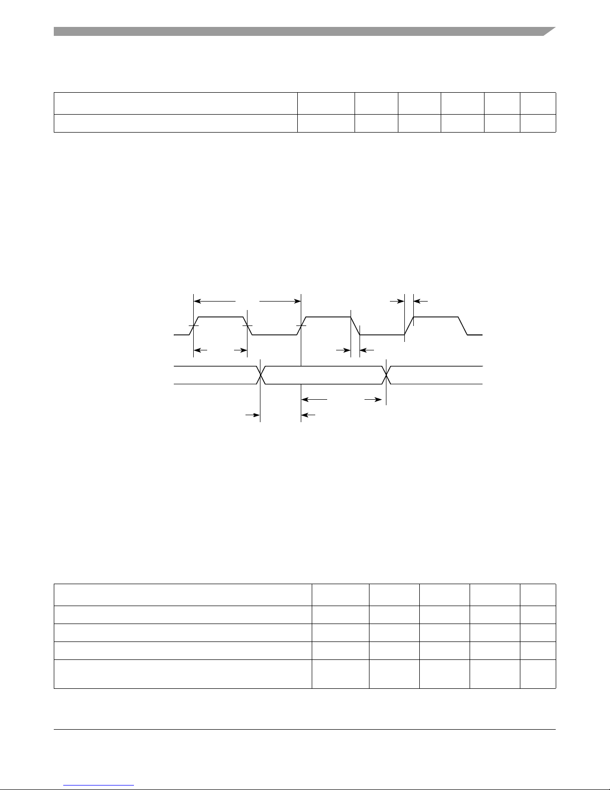
Table 28. GMII Receive AC Timing Specifications (continued)
RX_CLK
RXD[7:0]
t
GRDXKH
t
GRX
t
GRXH
t
GRXR
t
GRXF
t
GRDVKH
RX_DV
RX_ER
At recommended operating conditions with LVDD/OV
Parameter/Condition Symbol
of 3.3 V ± 10%.
DD
UCC Ethernet Controller: Three-Speed Ethernet, MII Management
1
Min Typ Max Unit Notes
RX_CLK clock fall time, (80% to 20%) t
GRXF
——1.0ns—
Notes:
1. The symbols used for timing specifications follow the pattern of t
inputs and t
(first two letters of functional block)(reference)(state)(signal)(state)
timing (GR) with respect to the time data input signals (D) reaching the valid state (V) relative to the t
going to the high state (H) or setup time. Also, t
input signals (D) went invalid (X) relative to the t
symbolizes GMII receive timing (GR) with respect to the time data
GRDXKL
clock reference (K) going to the low (L) state or hold time. Note that, in
GRX
(first two letters of functional block)(signal)(state)(reference)(state)
for outputs. For example, t
symbolizes GMII receive
GRDVKH
clock reference (K)
RX
general, the clock reference symbol representation is based on three letters representing the clock of a particular functional.
For example, the subscript of t
represents the GMII (G) receive (RX) clock. For rise and fall times, the latter convention
GRX
is used with the appropriate letter: R (rise) or F (fall).
2. In rev. 2.0 silicon, due to errata, t
QE_ENET18
in
Chip Errata for the MPC8360E, Rev. 1
GRDXKH
minimum is 0.5 which is not compliant with the standard. Refer to Errata
.
Figure 11 shows the GMII receive AC timing diagram.
for
Figure 11. GMII Receive AC Timing Diagram
8.2.2 MII AC Timing Specifications
This section describes the MII transmit and receive AC timing specifications.
8.2.2.1 MII Transmit AC Timing Specifications
Table 29 provides the MII transmit AC timing specifications.
Table 29. MII Transmit AC Timing Specifications
At recommended operating conditions with LVDD/OV
Parameter/Condition Symbol
TX_CLK clock period 10 Mbps t
TX_CLK clock period 100 Mbps t
TX_CLK duty cycle t
TX_CLK to MII data TXD[3:0], TX_ER, TX_EN delay t
MPC8360E/MPC8358E PowerQUICC II Pro Processor Revision 2.x TBGA Silicon Hardware Specifications, Rev. 4
Freescale Semiconductor 31
of 3.3 V ± 10%.
DD
MTX
MTX
MTXH/tMTX
MTKHDX
t
MTKHDV
1
Min Typ Max Unit
—400—ns
—40—ns
35 — 65 %
1
5—15ns
—
Page 32
UCC Ethernet Controller: Three-Speed Ethernet, MII Management
TX_CLK
TXD[3:0]
t
MTKHDX
t
MTX
t
MTXH
t
MTXR
t
MTXF
TX_EN
TX_ER
Table 29. MII Transmit AC Timing Specifications (continued)
At recommended operating conditions with LVDD/OV
Parameter/Condition Symbol
of 3.3 V ± 10%.
DD
1
Min Typ Max Unit
TX_CLK data clock rise time, (20% to 80%) t
TX_CLK data clock fall time, (80% to 20%) t
MTXR
MTXF
1.0 — 4.0 ns
1.0 — 4.0 ns
Note:
1. The symbols used for timing specifications follow the pattern of t
inputs and t
timing (MT) for the time t
(first two letters of functional block)(reference)(state)(signal)(state)
clock reference (K) going high (H) until data outputs (D) are invalid (X). Note that, in general,
MTX
(first two letters of functional block)(signal)(state)(reference)(state)
for outputs. For example, t
MTKHDX
symbolizes MII transmit
the clock reference symbol representation is based on two to three letters representing the clock of a particular functional.
For example, the subscript of t
represents the MII(M) transmit (TX) clock. For rise and fall times, the latter convention is
MTX
used with the appropriate letter: R (rise) or F (fall).
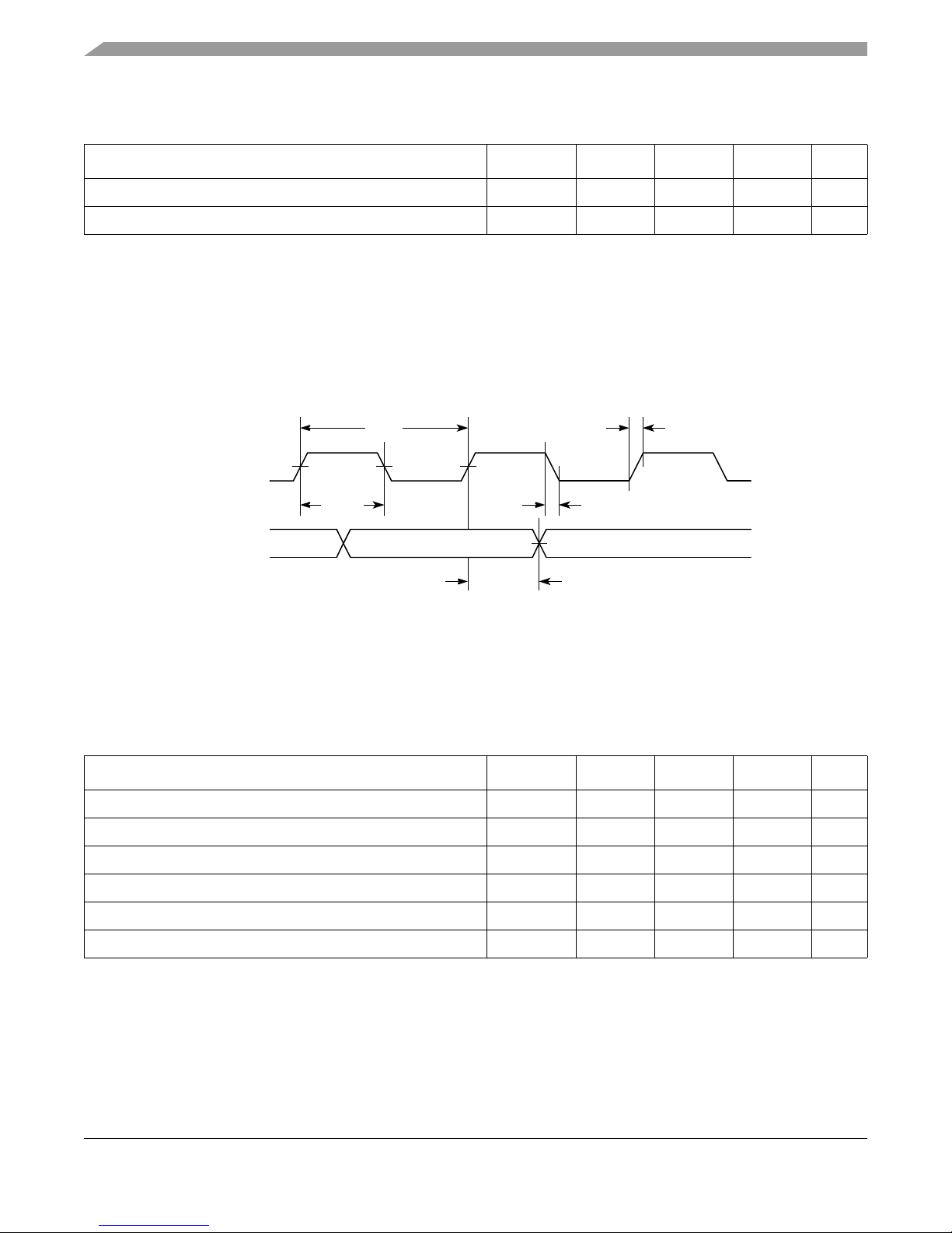
Figure 12 shows the MII transmit AC timing diagram.
Figure 12. MII Transmit AC Timing Diagram
for
8.2.2.2 MII Receive AC Timing Specifications
Table 30 provides the MII receive AC timing specifications.
At recommended operating conditions with LVDD/OV
Parameter/Condition Symbol
RX_CLK clock period 10 Mbps t
RX_CLK clock period 100 Mbps t
RX_CLK duty cycle t
RXD[3:0], RX_DV, RX_ER setup time to RX_CLK t
RXD[3:0], RX_DV, RX_ER hold time to RX_CLK t
RX_CLK clock rise time, (20% to 80%) t
MPC8360E/MPC8358E PowerQUICC II Pro Processor Revision 2.x TBGA Silicon Hardware Specifications, Rev. 4
32 Freescale Semiconductor
Table 30. MII Receive AC Timing Specifications
of 3.3 V ± 10%.
DD
MRXH/tMRX
MRX
MRX
MRDVKH
MRDXKH
MRXR
1
Min Typ Max Unit
—400—ns
—40—ns
35 — 65 %
10.0 — — ns
10.0 — — ns
1.0 — 4.0 ns
Page 33
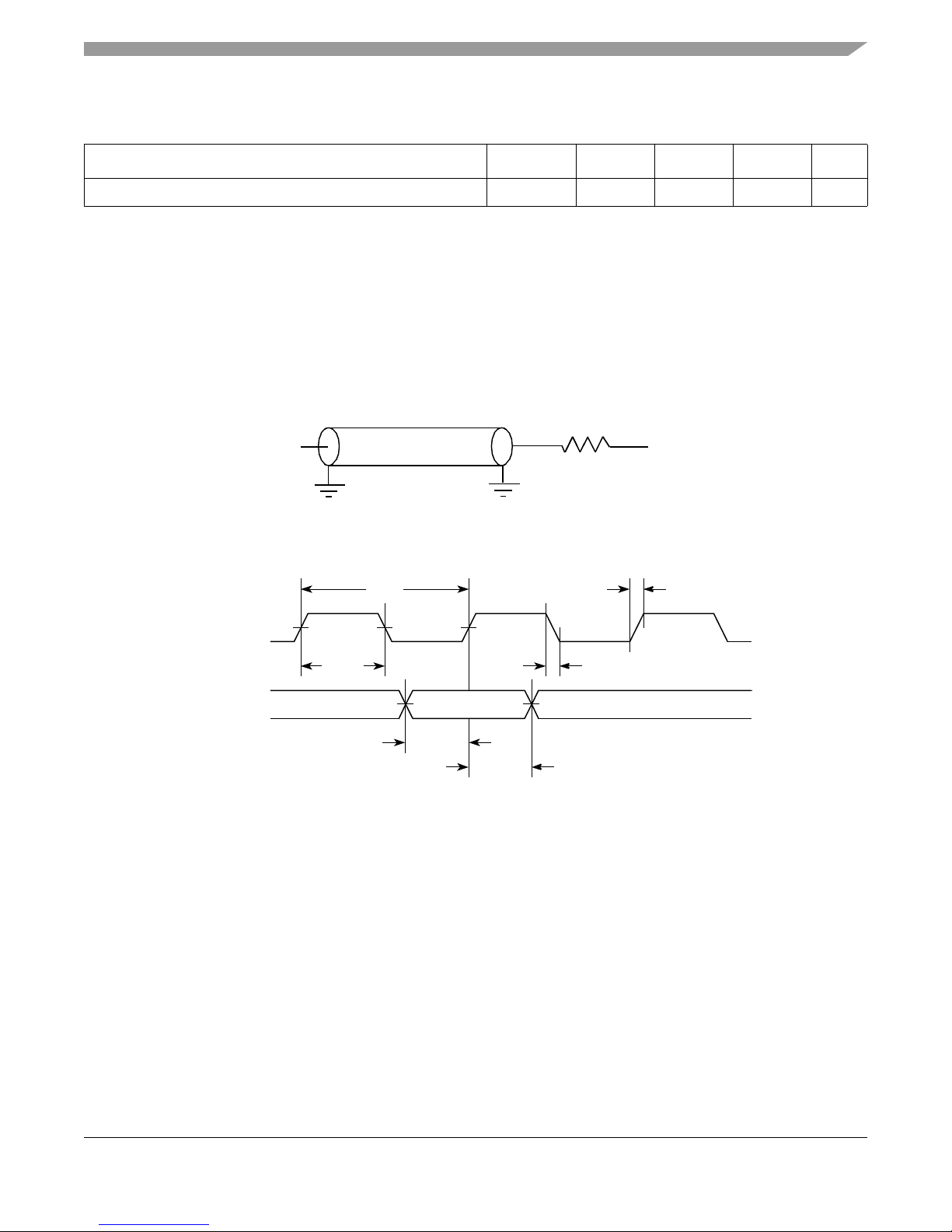
Table 30. MII Receive AC Timing Specifications (continued)
Output
Z0 = 50 Ω
LVDD/2
R
L
= 50 Ω
RX_CLK
RXD[3:0]
t
MRDXKH
t
MRX
t
MRXH
t
MRXR
t
MRXF
RX_DV
RX_ER
t
MRDVKH
Valid Data
At recommended operating conditions with LVDD/OV
Parameter/Condition Symbol
of 3.3 V ± 10%.
DD
UCC Ethernet Controller: Three-Speed Ethernet, MII Management
1
Min Typ Max Unit
RX_CLK clock fall time, (80% to 20%) t
MRXF
1.0 — 4.0 ns
Note:
1. The symbols used for timing specifications follow the pattern of t
inputs and t
(first two letters of f unctional block)(reference)(state)(signal)(state)
timing (MR) with respect to the time data input signals (D) reach the valid state (V) relative to the t
going to the high (H) state or setup time. Also, t
signals (D) went invalid (X) relative to the t
MRX
clock reference (K) going to the low (L) state or hold time. Note that, in general,
symbolizes MII receive timing (GR) with respect to the time data input
MRDXKL
(first two letters of functional block)(signal)(state)(reference)(state)
for outputs. For example, t
MRDVKH
symbolizes MII receive
clock reference (K)
MRX
the clock reference symbol representation is based on three letters representing the clock of a particular functional. For
example, the subscript of t
represents the MII (M) receive (RX) clock. For rise and fall times, the latter convention is used
MRX
with the appropriate letter: R (rise) or F (fall).
Figure 13 provides the AC test load.
Figure 13. AC Test Load
Figure 14 shows the MII receive AC timing diagram.
for
Figure 14. MII Receive AC Timing Diagram
MPC8360E/MPC8358E PowerQUICC II Pro Processor Revision 2.x TBGA Silicon Hardware Specifications, Rev. 4
Freescale Semiconductor 33
Page 34
UCC Ethernet Controller: Three-Speed Ethernet, MII Management
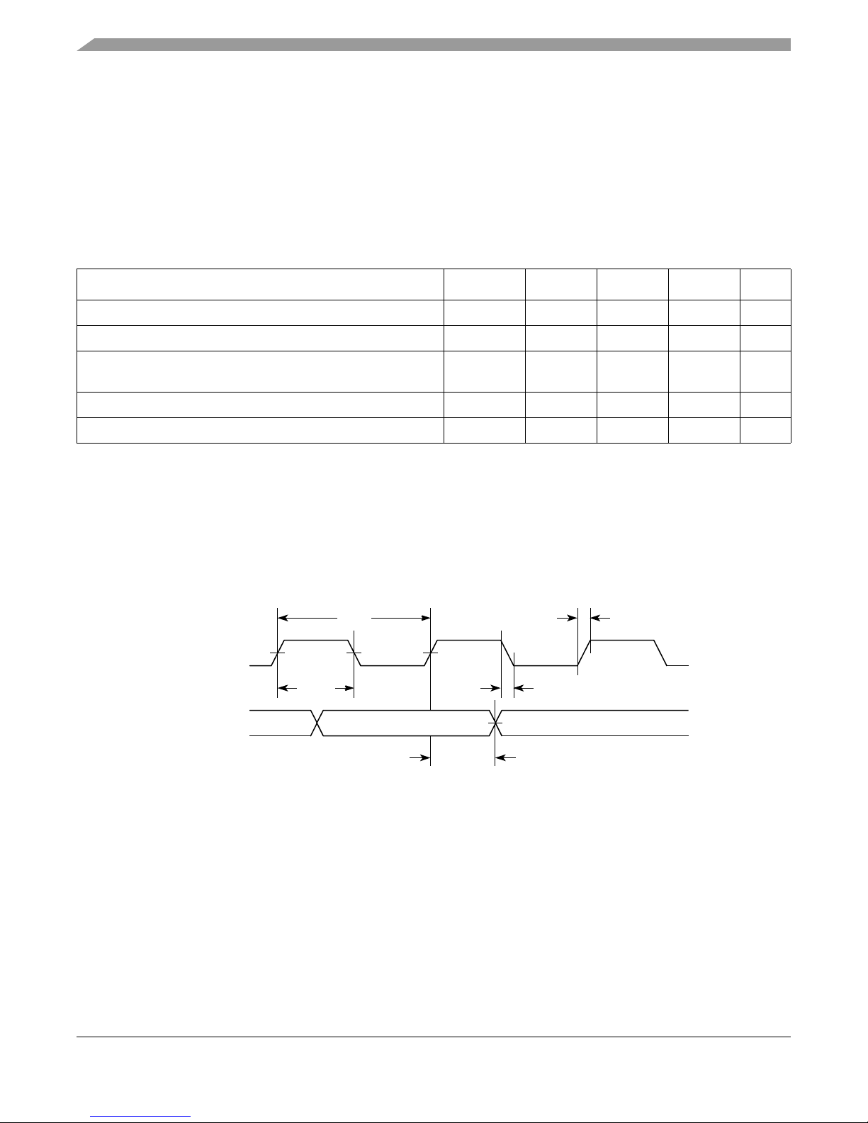
REF_CLK
TXD[1:0]
t
RMTKHDX
t
RMX
t
RMXH
t
RMXR
t
RMXF
TX_EN
8.2.3 RMII AC Timing Specifications
This section describes the RMII transmit and receive AC timing specifications.
8.2.3.1 RMII Transmit AC Timing Specifications
Table 31 provides the RMII transmit AC timing specifications.
Table 31. RMII Transmit AC Timing Specifications
At recommended operating conditions with LVDD/OV
Parameter/Condition Symbol
of 3.3 V ± 10%.
DD
1
Min Typ Max Unit
REF_CLK clock t
REF_CLK duty cycle t
REF_CLK to RMII data TXD[1:0], TX_EN delay t
RMXH/tRMX
RMTKHDX
t
RMTKHDV
REF_CLK data clock rise time t
REF_CLK data clock fall time t
RMX
RMXR
RMXF
—20—ns
35 — 65 %
2
——10ns
—
1.0 — 4.0 ns
1.0 — 4.0 ns
Note:
1. The symbols used for timing specifications follow the pattern of t
inputs and t
transmit timing (RMT) for the time t
(first two letters of functional block)(reference)(state)(signal)(state)
clock reference (K) going high (H) until data outputs (D) are invalid (X). Note that, in
RMX
(first three letters of functional block)(signal)(state)(reference)(state)
for outputs. For example, t
RMTKHD X
symbolizes RMII
general, the clock reference symbol representation is based on two to three letters representing the clock of a particular
functional. For example, the subscript of t
represents the RMII(RM) reference (X) clock. For rise and fall times, the latter
RMX
convention is used with the appropriate letter: R (rise) or F (fall).
Figure 15 shows the RMII transmit AC timing diagram.
for
Figure 15. RMII Transmit AC Timing Diagram
MPC8360E/MPC8358E PowerQUICC II Pro Processor Revision 2.x TBGA Silicon Hardware Specifications, Rev. 4
34 Freescale Semiconductor
Page 35
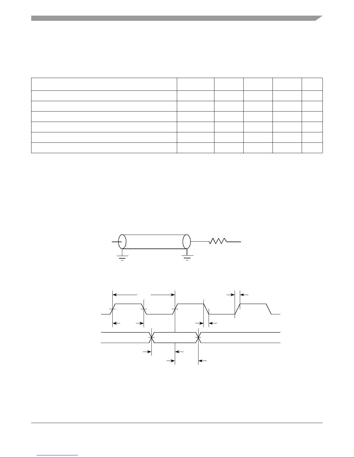
UCC Ethernet Controller: Three-Speed Ethernet, MII Management
Output
Z0 = 50 Ω
LVDD/2
R
L
= 50 Ω
REF_CLK
RXD[1:0]
t
RMRDXKH
t
RMX
t
RMXH
t
RMXR
t
RMXF
CRS_DV
RX_ER
t
RMRDVKH
Valid Data
8.2.3.2 RMII Receive AC Timing Specifications
Table 32 provides the RMII receive AC timing specifications.
At recommended operating conditions with LVDD/OV
Parameter/Condition Symbol
Table 32. RMII Receive AC Timing Specifications
of 3.3 V ± 10%.
DD
1
Min Typ Max Unit
REF_CLK clock period t
REF_CLK duty cycle t
RXD[1:0], CRS_DV, RX_ER setup time to REF_CLK t
RXD[1:0], CRS_DV, RX_ER hold time to REF_CLK t
RMXH/tRMX
RMRDVKH
RMRDXKH
REF_CLK clock rise time t
REF_CLK clock fall time t
RMX
RMXR
RMXF
—20—ns
35 — 65 %
4.0 — — ns
2.0 — — ns
1.0 — 4.0 ns
1.0 — 4.0 ns
Note:
1. The symbols used for timing specifications follow the pattern of t
inputs and t
(first two letters of functional block)(reference)(state)(signal)(state)
receive timing (RMR) with respect to the time data input signals (D) reach the valid state (V) relative to the t
reference (K) going to the high (H) state or setup time. Also, t
the time data input signals (D) went invalid (X) relative to the t
(first three letters of functional block)(signal)(state)(reference)(state)
for outputs. For example, t
RMRDXKL
RMX
symbolizes RMII receive timing (RMR) with respect to
clock reference (K) going to the low (L) state or hold time.
RMRDVKH
symbolizes RMII
RMX
clock
Note that, in general, the clock reference symbol representation is based on three letters representing the clock of a particular
functional. For example, the subscript of t
represents the RMII (RM) reference (X) clock. For rise and fall times, the latter
RMX
convention is used with the appropriate letter: R (rise) or F (fall).
Figure 16 provides the AC test load.
for
Figure 17 shows the RMII receive AC timing diagram.
MPC8360E/MPC8358E PowerQUICC II Pro Processor Revision 2.x TBGA Silicon Hardware Specifications, Rev. 4
Freescale Semiconductor 35
Figure 16. AC Test Load
Figure 17. RMII Receive AC Timing Diagram
Page 36
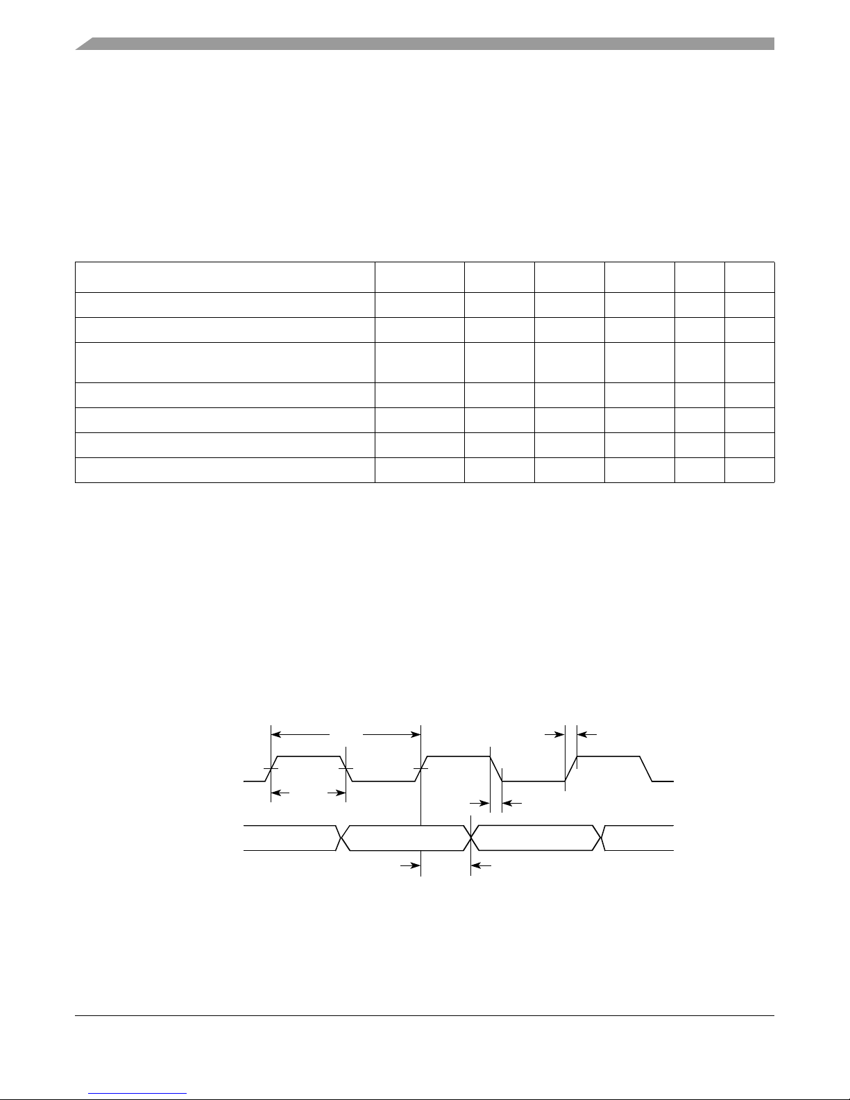
UCC Ethernet Controller: Three-Speed Ethernet, MII Management
GTX_CLK
TXD[7:0]
t
TTX
t
TTXH
t
TTXR
t
TTXF
t
TTKHDX
TX_EN
TX_ER
8.2.4 TBI AC Timing Specifications
This section describes the TBI transmit and receive AC timing specifications.
8.2.4.1 TBI Transmit AC Timing Specifications
Table 33 provides the TBI transmit AC timing specifications.
Table 33. TBI Transmit AC Timing Specifications
At recommended operating conditions with LVDD/OV
Parameter/Condition Symbol
of 3.3 V ± 10%.
DD
1
Min Typ Max Unit Notes
GTX_CLK clock period t
GTX_CLK duty cycle t
TTXH/tTTX
GTX_CLK to TBI data TCG[9:0] delay t
t
GTX_CLK clock rise time, (20% to 80%) t
GTX_CLK clock fall time, (80% to 20%) t
GTX_CLK125 reference clock period t
GTX_CLK125 reference clock duty cycle t
G125H/tG125
TTX
TTKHDX
TTKHDV
TTXR
TTXF
G125
—8.0—ns—
40 — 60 % —
1.0
—
——
5.0
ns 3
——1.0ns—
——1.0ns—
—8.0—ns2
45 — 55 ns —
Notes:
1. The symbols used for timing specifications follow the pattern of t
inputs and t
transmit timing (TT) with respect to the time from t
state (V) or setup time. Also, t
(first two letters of functional block)(reference)(state)(signal)(state)
TTKHDX
symbolizes the TBI transmit timing (TT) with respect to the time from t
(K) going high (H) until the referenced data signals (D) reach the valid
TTX
(first two letters of functional block)(signal)(state )(reference)(state)
for outputs. For example, t
symbolizes the TBI
TTKHDV
(K) going high
TTX
(H) until the referenced data signals (D) reach the invalid state (X) or hold time. Note that, in general, the clock reference
symbol representation is based on three letters representing the clock of a particular functional. For example, the subscript
of t
represents the TBI (T) transmit (TX) clock. For rise and fall times, the latter convention is used with the appropriate
TTX
letter: R (rise) or F (fall).
2. This symbol is used to represent the external GTX_CLK125 and does not follow the original symbol naming convention.
3. In rev. 2.0 silicon, due to errata, t
MPC8360E, Rev. 1
.
minimum is 0.7 ns for UCC1. Refer to Errata
TTKHDX
QE_ENET19
in
Chip Errata for the
Figure 18 shows the TBI transmit AC timing diagram.
for
MPC8360E/MPC8358E PowerQUICC II Pro Processor Revision 2.x TBGA Silicon Hardware Specifications, Rev. 4
36 Freescale Semiconductor
Figure 18. TBI Transmit AC Timing Diagram
Page 37
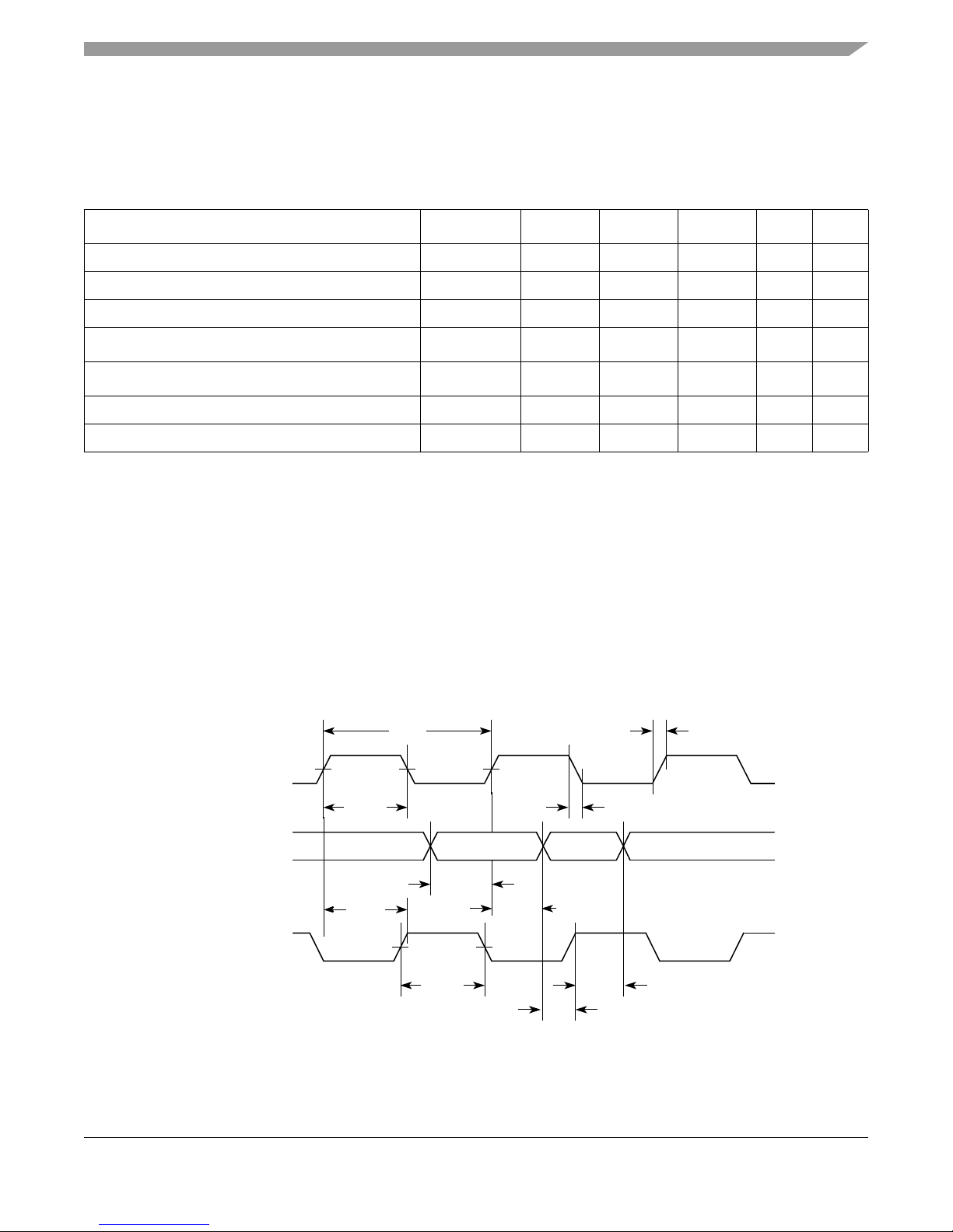
UCC Ethernet Controller: Three-Speed Ethernet, MII Management
PMA_RX_CLK1
RCG[9:0]
t
TRX
t
TRXH
t
TRXR
t
TRXF
t
TRDVKH
PMA_RX_CLK0
t
TRDXKH
t
TRDVKH
t
TRDXKH
t
SKTRX
t
TRXH
Even RCG Odd RCG
8.2.4.2 TBI Receive AC Timing Specifications
Table 34 provides the TBI receive AC timing specifications.
Table 34. TBI Receive AC Timing Specifications
At recommended operating conditions with LVDD/OV
Parameter/Condition Symbol
of 3.3 V ± 10%.
DD
1
Min Typ Max Unit Notes
PMA_RX_CLK clock period t
PMA_RX_CLK skew t
RX_CLK duty cycle t
RCG[9:0] setup time to rising PMA_RX_CLK
RCG[9:0] hold time to rising PMA_RX_CLK
RX_CLK clock rise time, V
RX_CLK clock fall time, V
(min) to VIH(max) t
IL
(max) to VIL(min) t
IH
TRXH/tTRX
t
t
TRDXKH
TRX
SKTRX
TRDVKH
TRXR
TRXF
— 16.0 — ns —
7.5 — 8.5 ns —
40 — 60 % —
2.5 — — ns 2
1.0 — — ns 2
0.7 — 2.4 ns —
0.7 — 2.4 ns —
Notes:
1. The symbols used for timing specifications follow the pattern of t
inputs and t
(first two letters of functional block)(reference)(state)(signal)(state)
(first two letters of functional block)(signal)(state)(reference)(state)
for outputs. For example, t
timing (TR) with respect to the time data input signals (D) reach the valid state (V) relative to the t
going to the high (H) state or setup time. Also, t
signals (D) went invalid (X) relative to the t
TRX
clock reference (K) going to the high (H) state. Note that, in general, the clock
symbolizes TBI receive timing (TR) with respect to the time data input
TRDXKH
symbolizes TBI receive
TRDVKH
clock reference (K)
TRX
for
reference symbol representation is based on three letters representing the clock of a particular functional. For example, the
subscript of t
represents the TBI (T) receive (RX) clock. For rise and fall times, the latter convention is used with the
TRX
appropriate letter: R (rise) or F (fall). For symbols representing skews, the subscript is skew (SK) followed by the clock that
is being skewed (TRX).
2. Setup and hold time of even numbered RCG are measured from riding edge of PMA_RX_CLK1. Setup and hold time of odd
numbered RCG are measured from riding edge of PMA_RX_CLK0.
Figure 19 shows the TBI receive AC timing diagram.
Figure 19. TBI Receive AC Timing Diagram
MPC8360E/MPC8358E PowerQUICC II Pro Processor Revision 2.x TBGA Silicon Hardware Specifications, Rev. 4
Freescale Semiconductor 37
Page 38
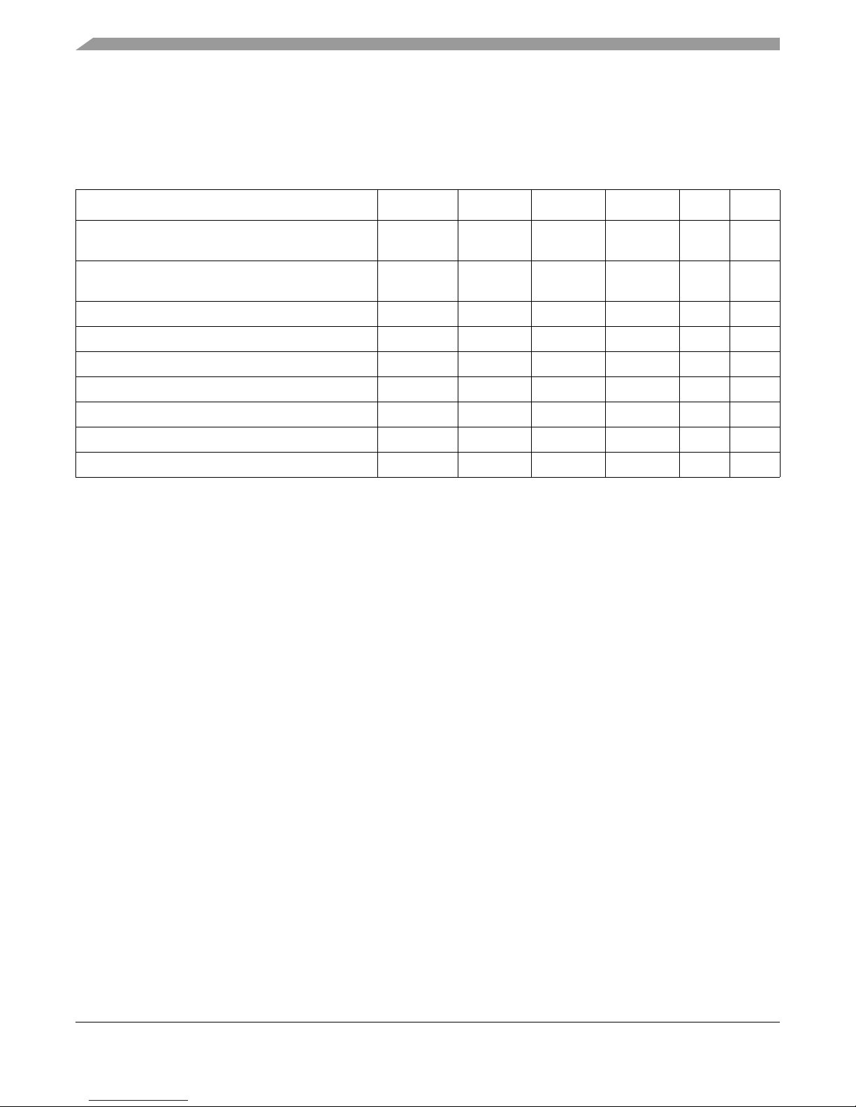
UCC Ethernet Controller: Three-Speed Ethernet, MII Management
8.2.5 RGMII and RTBI AC Timing Specifications
Table 35 presents the RGMII and RTBI AC timing specifications.
Table 35. RGMII and RTBI AC Timing Specifications
At recommended operating conditions with LVDD of 2.5 V ± 5%.
RGT
RGTR
RGTF
G125
1
Min Typ Max Unit Notes
–0.5
—
1.0
—
——
ns 7
0.5
——
ns 2
2.6
7.2 8.0 8.8 ns 3
45 50 55 % 4, 5
40 50 60 % 3, 5
— — 0.75 ns —
— — 0.75 ns —
—8.0—ns6
47 — 53 % —
Parameter/Condition Symbol
Data to clock output skew (at transmitter) t
Data to clock input skew (at receiver) t
SKRGTKHDX
t
SKRGTKHDV
SKRGDXKH
t
SKRGDVKH
Clock cycle duration t
Duty cycle for 1000Base-T t
Duty cycle for 10BASE-T and 100BASE-TX t
RGTH/tRGT
RGTH/tRGT
Rise time (20–80%) t
Fall time (20–80%) t
GTX_CLK125 reference clock period t
GTX_CLK125 reference clock duty cycle t
G125H/tG125
Notes:
1. Note that, in general, the clock reference symbol representation for this section is based on the symbols RGT to represent
RGMII and RTBI timing. For example, the subscript of t
represents the TBI (T) receive (Rx) clock. Note also that the
RGT
notation for rise (R) and fall (F) times follows the clock symbol that is being represented. For symbols representing skews,
the subscript is skew (SK) followed by the clock that is being skewed (RGT).
2. This implies that PC board design will require clocks to be routed such that an additional trace delay of greater than 1.5 ns
will be added to the associated clock signal.
3. For 10 and 100 Mbps, t
scales to 400 ns ± 40 ns and 40 ns ± 4 ns, respectively.
RGT
4. Duty cycle may be stretched/shrunk during speed changes or while transitioning to a received packet's clock domains as long
as the minimum duty cycle is not violated and stretching occurs for no more than three t
of the lowest speed transitioned
RGT
between.
5. Duty cycle reference is LV
DD
/2.
6. This symbol is used to represent the external GTX_CLK125 and does not follow the original symbol naming convention.
7. In rev. 2.0 silicon, due to errata, t
SKRGTKHDX
option 1, and 1.8 ns for UCC2 option 2. In rev. 2.1 silicon, due to errata, t
and –0.9 for UCC2 option 2, and t
Refer to Errata QE_ENET10 in
SKRGTKHDV
Chip Errata for the MPC8360E, Rev. 1
minimum is –2.3 ns and t
SKRGTKHDV
SKRGTKHDX
maximum is 1 ns for UCC1, 1.2 ns for UCC2
minimum is –0.65 ns for UCC2 option 1
maximum is 0.75 ns for UCC1 and UCC2 option 1 and 0.85 for UCC2 option 2.
. UCC1 does meet t
SKRGTKHDX
minimum for rev. 2.1
silicon.
MPC8360E/MPC8358E PowerQUICC II Pro Processor Revision 2.x TBGA Silicon Hardware Specifications, Rev. 4
38 Freescale Semiconductor
Page 39
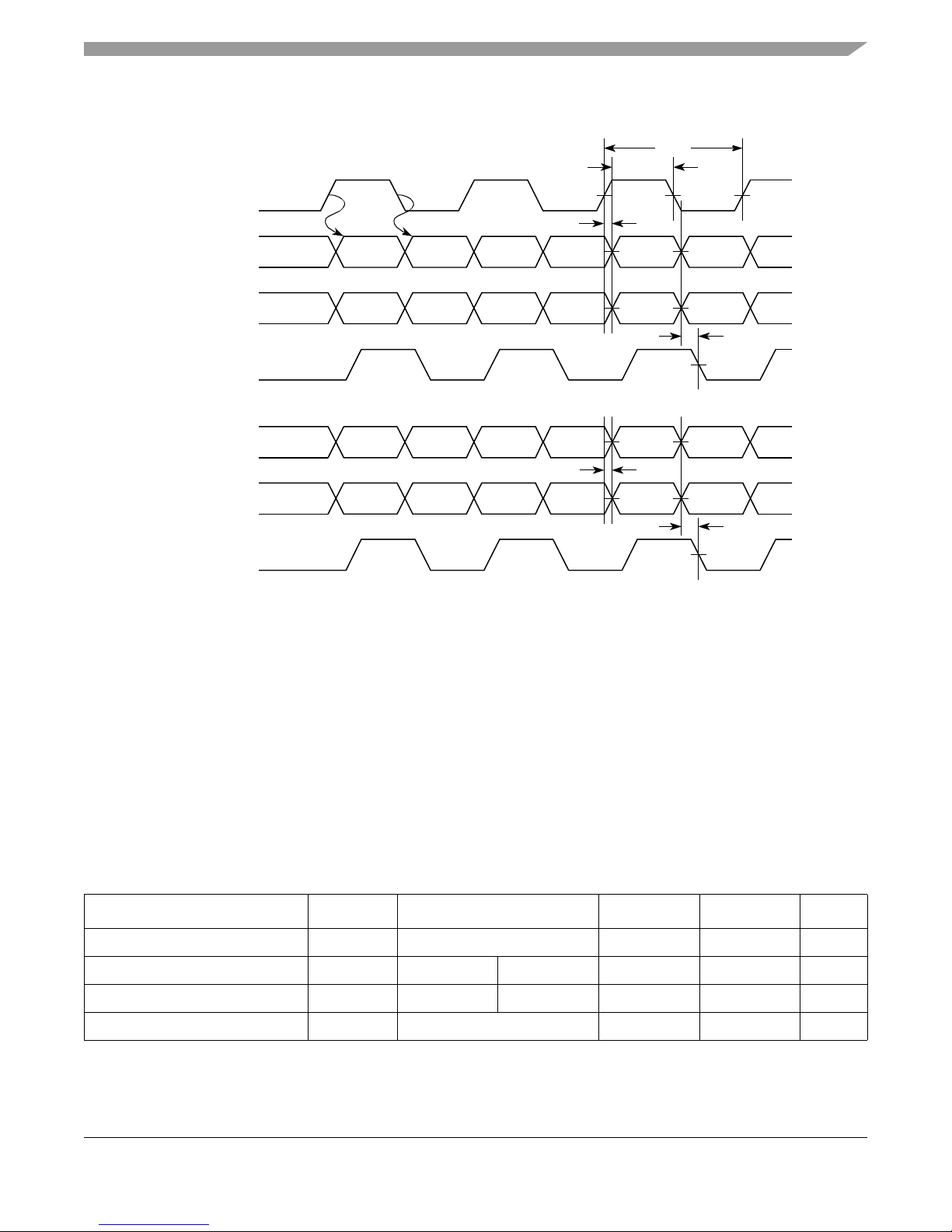
UCC Ethernet Controller: Three-Speed Ethernet, MII Management
GTX_CLK
t
RGT
t
RGTH
t
SKRGTKHDX
TX_CTL
TXD[8:5]
TXD[7:4]
TXD[9]
TXERR
TXD[4]
TXEN
TXD[3:0]
(At Transmitter)
TXD[8:5][3:0]
TXD[7:4][3:0]
TX_CLK
(At PHY)
RX_CTL
RXD[8:5]
RXD[7:4]
RXD[9]
RXERR
RXD[4]
RXDV
RXD[3:0]
RXD[8:5][3:0]
RXD[7:4][3:0]
RX_CLK
(At PHY)
t
SKRGTKHDX
t
SKRGTKHDX
t
SKRGTKHDX
Figure 20 shows the RGMII and RTBI AC timing and multiplexing diagrams.
8.3 Ethernet Management Interface Electrical Characteristics
The electrical characteri stics specified here apply to MII management interface signals MDI O
(management data input/output) and MDC (management data clock). The electrical char acter i stics for
GMII, RGMII, TBI, and RTBI are specified in Section 8.1, “Three-Speed Ethernet Cont roller
(10/100/1000 Mbps)— GMII/MII/RMII/TBI/RGMII/RTBI Electrical Characteristics.”
8.3.1 MII Management DC Electrical Characteristics
The MDC and MDIO are defined to operate at a supply voltage of 3.3 V . T he DC electrical characteristics
for MDIO and MDC are provided in Table 36.
Supply voltage (3.3 V) OV
Output high voltage V
Output low voltage V
Input high voltage V
Figure 20. RGMII and RTBI AC Timing and Multiplexing Diagrams
Table 36. MII Management DC Electrical Characteristics When Powered at 3.3 V
Parameter Symbol Conditions Min Max Unit
DD
OH
OL
IH
I
= –1.0 mA OV
OH
I
= 1.0 mA OV
OL
— 2.97 3.63 V
= Min 2.10 OVDD + 0.3 V
DD
DD
—2.00—V
= Min GND 0.50 V
MPC8360E/MPC8358E PowerQUICC II Pro Processor Revision 2.x TBGA Silicon Hardware Specifications, Rev. 4
Freescale Semiconductor 39
Page 40
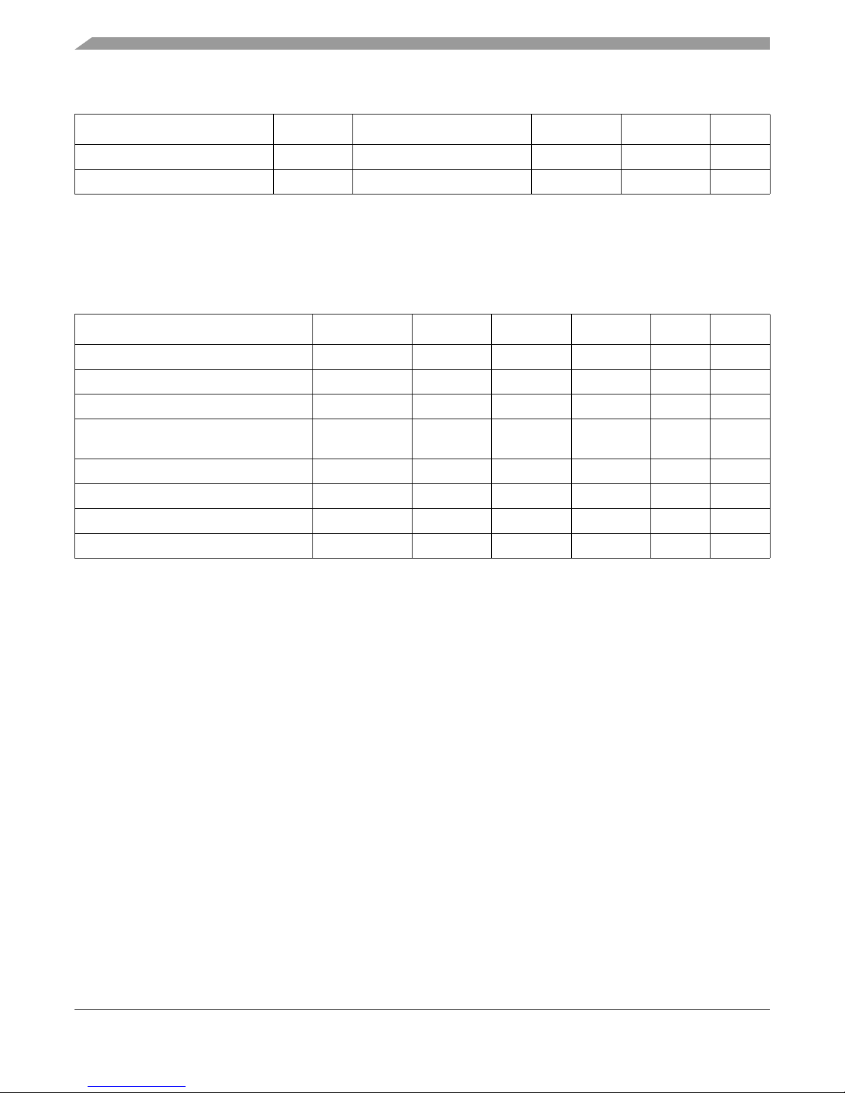
UCC Ethernet Controller: Three-Speed Ethernet, MII Management
Table 36. MII Management DC Electrical Characteristics When Powered at 3.3 V (continued)
Parameter Symbol Conditions Min Max Unit
Input low voltage V
Input current I
IL
IN
0 V ≤ VIN ≤ OV
——0.80V
DD
—±10μA
8.3.2 MII Management AC Electrical Specifications
Table 37 provides the MII management AC timing specifications.
Table 37. MII Management AC Timing Specifications
At recommended operating conditions with LVDD is 3.3 V ± 10%.
MDC
MDC
MDCH
MDCR
MDHF
1
Min Typ Max Unit Notes
—2.5—MHz2
—400—ns—
32 — — ns —
10
—
——
110
ns 3
10 — — ns —
0——ns—
— — 10 ns —
— — 10 ns —
(first two letters of functional block)(signal)(state)(reference)(state)
for outputs. For example, t
MDKHDX
symbolizes management
for
Parameter/Condition Symbol
MDC frequency f
MDC period t
MDC clock pulse width high t
MDC to MDIO delay t
MDIO to MDC setup time t
MDIO to MDC hold time t
MDTKHDX
t
MDTKHDV
MDRDVKH
MDRDXKH
MDC rise time t
MDC fall time t
Notes:
1. The symbols used for timing specifications follow the pattern of t
inputs and t
data timing (MD) for the time t
Also, t
(V) relative to the t
(first two letters of functional block)(reference)(state)(signal)(state)
MDRDVKH
symbolizes management data timing (MD) with respect to the time data input signals (D) reach the valid state
clock reference (K) going to the high (H) state or setup time. For rise and fall times, the latter
MDC
from clock reference (K) high (H) until data outputs (D) are invalid (X) or data hold time.
MDC
convention is used with the appropriate letter: R (rise) or F (fall).
2. This parameter is dependent on the csb_clk speed (that is, for a csb_clk of 267 MHz, the maximum frequency is 8.3 MHz
and the minimum frequency is 1.2 MHz; for a csb_clk of 375 MHz, the maximum frequency is 11.7 MHz and the minimum
frequency is 1.7 MHz).
3. This parameter is dependent on the ce_clk speed (that is, for a ce_clk of 200 MHz, the delay is 90 ns and for a ce_clk of
300 MHz, the delay is 63 ns).
MPC8360E/MPC8358E PowerQUICC II Pro Processor Revision 2.x TBGA Silicon Hardware Specifications, Rev. 4
40 Freescale Semiconductor
Page 41
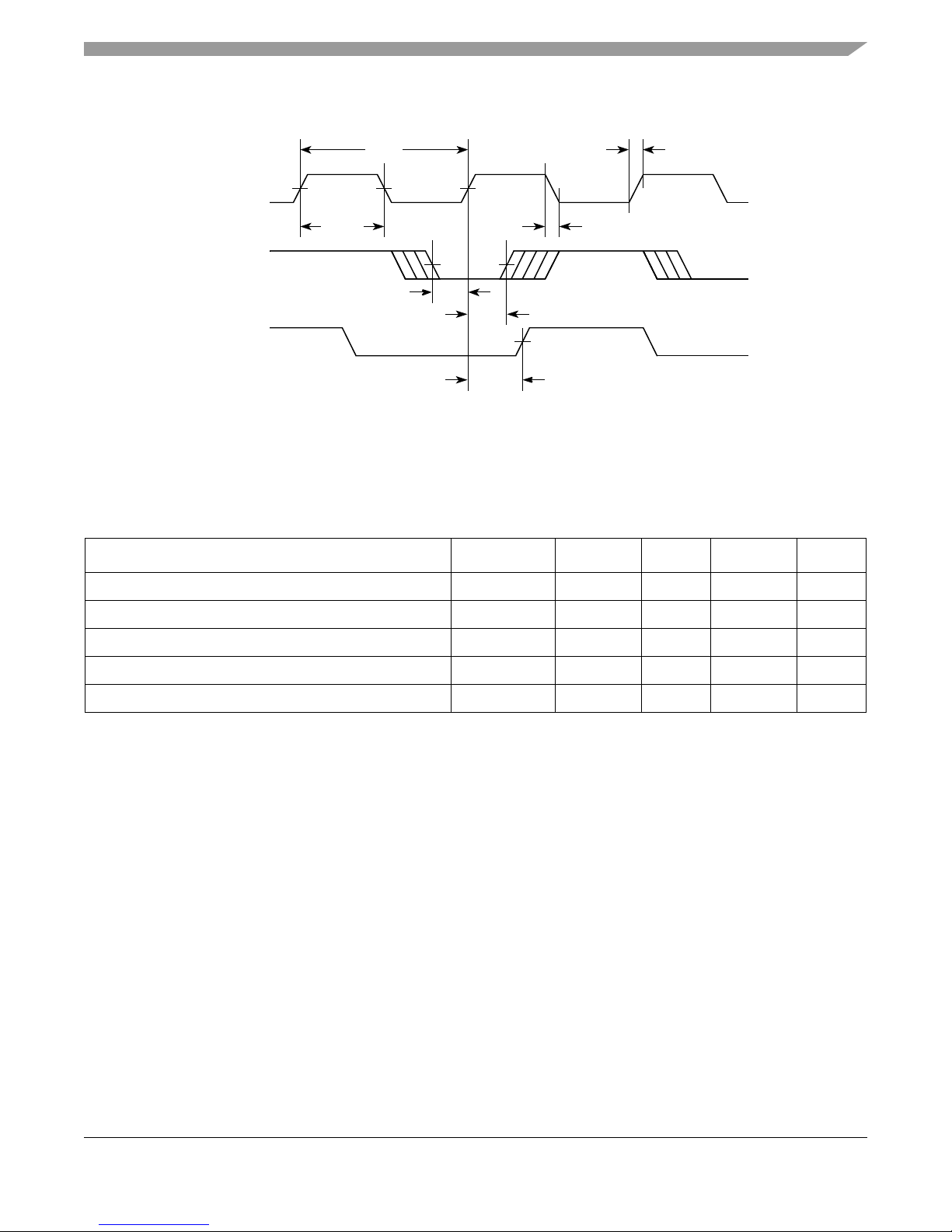
Figure 21 shows the MII management AC timing diagram.
MDC
t
MDRDXKH
t
MDC
t
MDCH
t
MDCR
t
MDHF
t
MDTKHDX
MDIO
MDIO
(Input)
(Output)
t
MDRDVKH
Figure 21. MII Management Interface Timing Diagram
8.3.3 IEEE 1588 Timer AC Specifications
Table 38 provides the IEEE 1588 timer AC specifications.
Table 38. IEEE 1588 Timer AC Specifications
Local Bus
Parameter Symbol Min Max Unit Notes
Timer clock frequency t
Input setup to timer clock t
Input hold from timer clock t
Output clock to output valid t
Timer alarm to output valid t
TMRCK
TMRCKS
TMRCKH
GCLKNV
TMRAL
070MHz1
———2, 3
———2, 3
06ns—
——— 2
Notes:
1. The timer can operate on rtc_clock or tmr_clock. These clocks get muxed and any one of them can be selected. The
minimum and maximum requirement for both rtc_clock and tmr_clock are the same.
2. These are asynchronous signals.
3. Inputs need to be stable at least one TMR clock.
9 Local Bus
This section describes the DC and AC electrical specif icat ions for the local bus interf ace of the
MPC8360E/58E.
MPC8360E/MPC8358E PowerQUICC II Pro Processor Revision 2.x TBGA Silicon Hardware Specifications, Rev. 4
Freescale Semiconductor 41
Page 42
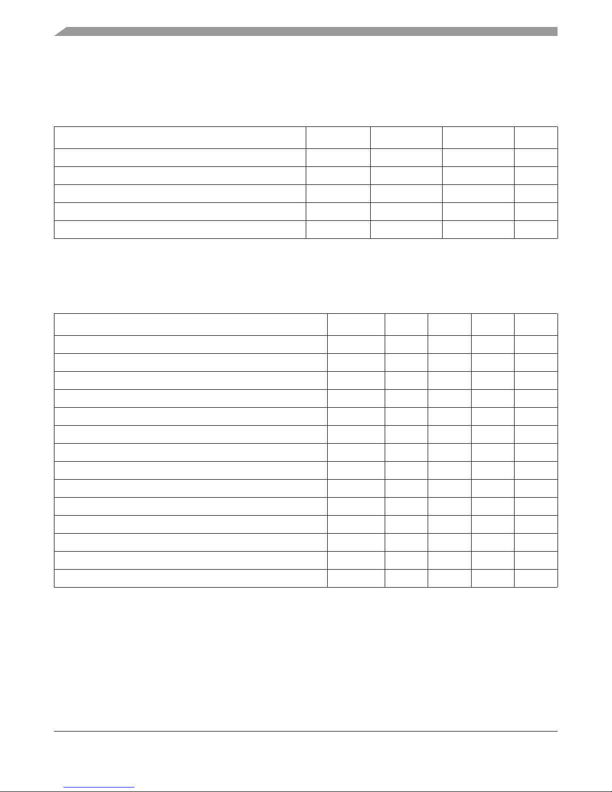
Local Bus
9.1 Local Bus DC Electrical Characteristics
Table 39 provides the DC electrical characteristics for the local bus interface.
Table 39. Local Bus DC Electrical Characteristics
Parameter Symbol Min Max Unit
High-level input voltage V
Low-level input voltage V
High-level output voltage, I
Low-level output voltage, I
= –100 μAV
OH
= 100 μAV
OL
Input current I
IH
IL
OH
OL
IN
2OV
DD
–0.3 0.8 V
OVDD – 0.4 — V
—0.2V
—±10μA
9.2 Local Bus AC Electrical Specifications
Table 40 describes the general timing parameters of the local bus interface of the device.
Table 40. Local Bus General Timing Parameters—DLL Enabled
LBK
LBIVKH1
LBIVKH2
LBIXKH1
LBIXKH2
LBOTOT1
LBOTOT2
LBOTOT3
LBKHLR
LBKHOV1
LBKHOV2
LBKHOV3
LBKHOX1
LBKHOX2
1
Min Max Unit Notes
7.5 — ns 2
1.7 — ns 3, 4
1.9 — ns 3, 4
1.0 — ns 3, 4
1.0 — ns 3, 4
1.5 — ns 5
3.0 — ns 6
2.5 — ns 7
—4.5ns —
—4.5ns —
—4.5ns 3
—4.5ns 3
1.0 — ns 3
1.0 — ns 3
Parameter Symbol
Local bus cycle time t
Input setup to local bus clock (except LUPWAIT) t
LUPWAIT input setup to local bus clock t
Input hold from local bus clock (except LUPWAIT) t
LUPWAIT input hold from local bus clock t
LALE output fall to LAD output transition (LATCH hold time) t
LALE output fall to LAD output transition (LATCH hold time) t
LALE output fall to LAD output transition (LATCH hold time) t
Local bus clock to LALE rise t
Local bus clock to output valid (except LAD/LDP and LALE) t
Local bus clock to data valid for LAD/LDP t
Local bus clock to address valid for LAD t
Output hold from local bus clock (except LAD/LDP and LALE) t
Output hold from local bus clock for LAD/LDP t
+ 0.3 V
MPC8360E/MPC8358E PowerQUICC II Pro Processor Revision 2.x TBGA Silicon Hardware Specifications, Rev. 4
42 Freescale Semiconductor
Page 43
Table 40. Local Bus General Timing Parameters—DLL Enabled (continued)
Local Bus
LBKHOZ
1
Min Max Unit Notes
—3.8ns —
Parameter Symbol
Local bus clock to output high impedance for LAD/LDP t
Notes:
1. The symbols used for timing specifications follow the pattern of t
inputs and t
(first two letters of functional block)(reference)(state)(signal)(state)
timing (LB) for the input (I) to go invalid (X) with respect to the time the t
clock one (1). Also, t
symbolizes local bus timing (LB) for the t
LBKHOX
(first two letters of functional block)(signal)(state)(reference)(state)
for outputs. For example, t
clock reference (K) goes high (H), in this case for
LBK
clock reference (K) to go high (H), with respect to
LBK
symbolizes local bus
LBIXKH1
the output (O) going invalid (X) or output hold time.
2. All timings are in reference to rising edge of LSYNC_IN.
3. All signals are measured from OV
/2 of the rising edge of LSYNC_IN to 0.4 × OVDD of the signal in question for 3.3-V
DD
signaling levels.
4. Input timings are measured at the pin.
5. t
LBOTOT1
should be used when RCWH[LALE] is not set and when the load on LALE output pin is at least 10 pF less than the
load on LAD output pins.
6. t
LBOTOT2
should be used when RCWH[LALE] is set and when the load on LALE output pin is at least 10 pF less than the load
on LAD output pins.
7. t
LBOTOT3
should be used when RCWH[LALE] is set and when the load on LALE output pin equals to the load on LAD output
pins.
8. For purposes of active/float timing measurements, the Hi-Z or off-state is defined to be when the total current delivered
through the component pin is less than or equal to the leakage current specification.
Table 41 describes the general timing parameters of the local bus interface of the device.
Table 41. Local Bus General Timing Parameters—DLL Bypass Mode
for
Parameter Symbol
Local bus cycle time t
Input setup to local bus clock t
Input hold from local bus clock t
LALE output fall to LAD output transition (LATCH hold time) t
LALE output fall to LAD output transition (LATCH hold time) t
LALE output fall to LAD output transition (LATCH hold time) t
LBOTOT1
LBOTOT2
LBOTOT3
Local bus clock to output valid t
LBK
LBIVKH
LBIXKH
LBKHOV
1
Min Max Unit Notes
15 — ns 2
7—ns3, 4
1.0 — ns 3, 4
1.5 — ns 5
3—ns6
2.5 — ns 7
—3ns3
MPC8360E/MPC8358E PowerQUICC II Pro Processor Revision 2.x TBGA Silicon Hardware Specifications, Rev. 4
Freescale Semiconductor 43
Page 44
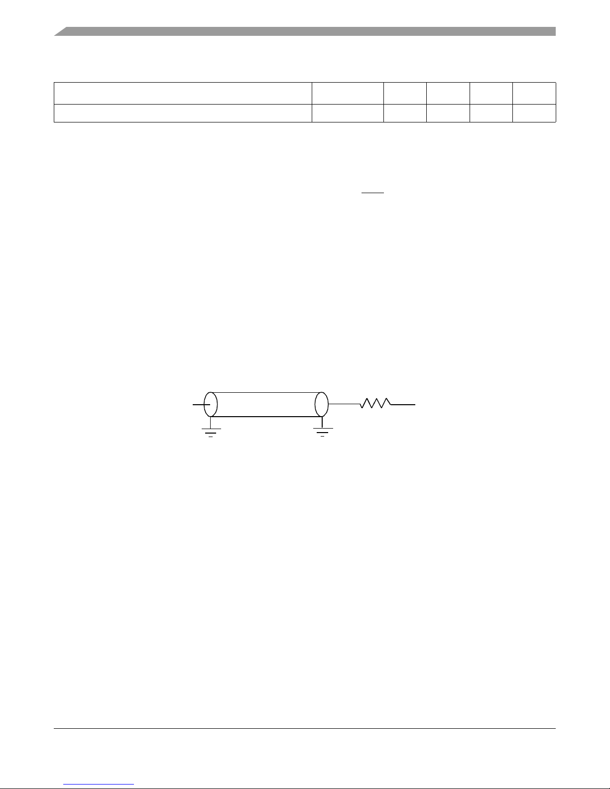
Local Bus
Output
Z0 = 50 Ω
OVDD/2
R
L
= 50 Ω
Table 41. Local Bus General Timing Parameters—DLL Bypass Mode (continued)
LBKHOZ
1
Min Max Unit Notes
—4ns—
Parameter Symbol
Local bus clock to output high impedance for LAD/LDP t
Notes:
1. The symbols used for timing specifications follow the pattern of t
inputs and t
(first two letters of functional block)(reference)(state)(signal)(state)
timing (LB) for the input (I) to go invalid (X) with respect to the time the t
clock one (1). Also, t
symbolizes local bus timing (LB) for the t
LBKHOX
(first two letters of functional block)(signal)(state)(reference)(state)
for outputs. For example, t
clock reference (K) goes high (H), in this case for
LBK
clock reference (K) to go high (H), with respect to
LBK
symbolizes local bus
LBIXKH1
the output (O) going invalid (X) or output hold time.
2. All timings are in reference to falling edge of LCLK0 (for all outputs and for LGTA
and LUPWAIT inputs) or rising edge of
LCLK0 (for all other inputs).
3. All signals are measured from OV
/2 of the rising/falling edge of LCLK0 to 0.4 × OVDD of the signal in question for 3.3-V
DD
signaling levels.
4. Input timings are measured at the pin.
5. t
LBOTOT1
should be used when RCWH[LALE] is not set and when the load on LALE output pin is at least 10 pF less than the
load on LAD output pins.
6. t
LBOTOT2
should be used when RCWH[LALE] is set and when the load on LALE output pin is at least 10 pF less than the load
on LAD output pins.
7. t
LBOTOT3
should be used when RCWH[LALE] is set and when the load on LALE output pin equals to the load on LAD output
pins.
8. For purposes of active/float timing measurements, the Hi-Z or off-state is defined to be when the total current delivered
through the component pin is less than or equal to the leakage current specification.
9. DLL bypass mode is not recommended for use at frequencies above 66 MHz.
Figure 22 provides the AC test load for the local bus.
for
MPC8360E/MPC8358E PowerQUICC II Pro Processor Revision 2.x TBGA Silicon Hardware Specifications, Rev. 4
44 Freescale Semiconductor
Figure 22. Local Bus C Test Load
Page 45
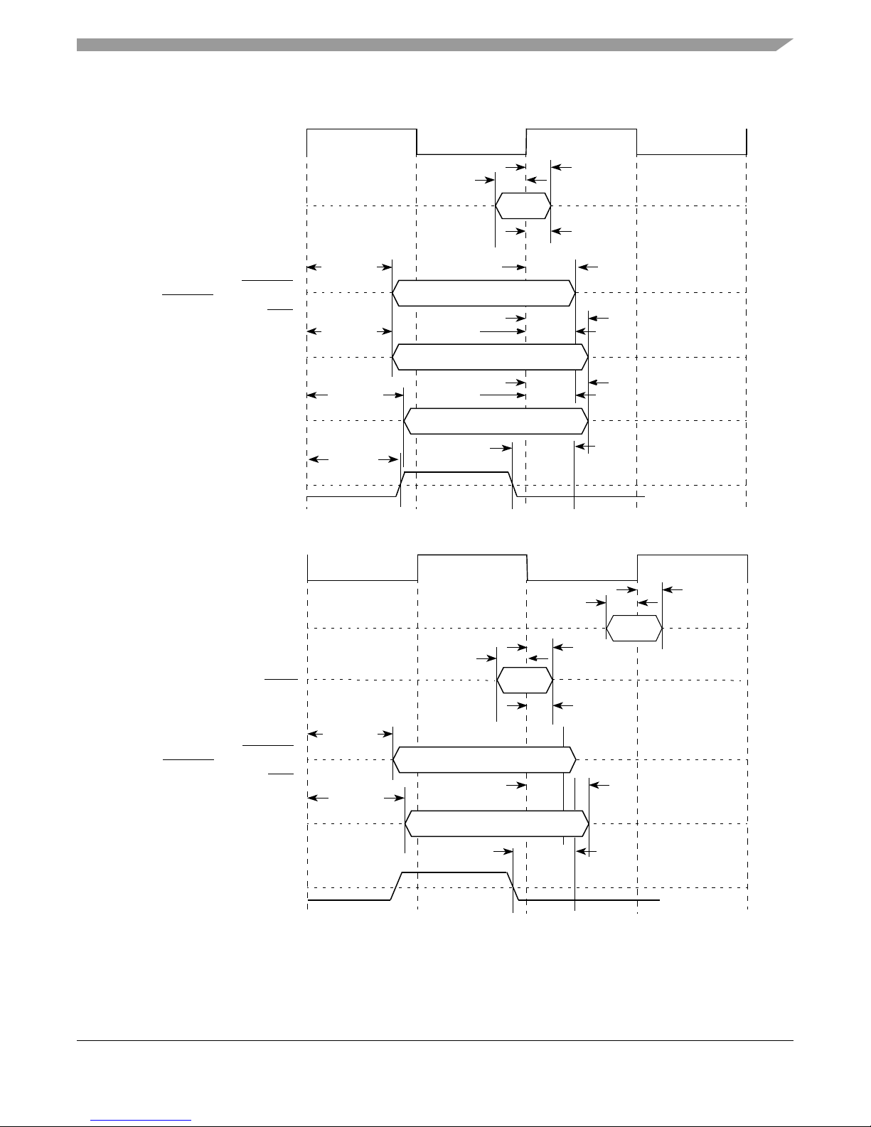
Figure 23 through Figure 28 show the local bus signals.
Output Signals:
LA[27:31]/LBCTL/LBCKE/LOE
/
LSDA10/LSDWE/LSDRAS
/
LSDCAS
/LSDDQM[0:3]
t
LBKHOV
t
LBKHOV
t
LBKHOV
LSYNC_IN
Input Signals:
LAD[0:31]/LDP[0:3]
Output (Data) Signals:
LAD[0:31]/LDP[0:3]
Output (Address) Signal:
LAD[0:31]
LALE
t
LBIXKH
t
LBIVKH
t
LBIXKH
t
LBKHOX
t
LBKHOX
t
LBKHOZ
t
LBKHLR
t
LBOTOT
t
LBKHOZ
t
LBKHOX
Output Signals:
LA[27:31]/LBCTL/LBCKE/LOE
/
LSDA10/LSDWE/LSDRAS
/
LSDCAS
/LSDDQM[0:3]
t
LBKHOV
t
LBKHOV
LCLK[n]
Input Signals:
LAD[0:31]/LDP[0:3]
Output Signals:
LAD[0:31]/LDP[0:3]
t
LBIXKH
t
LBIVKH
t
LBKHOZ
t
LBOTOT
LALE
Input Signal:
LGTA
t
LBIXKH
t
LBIVKH
t
LBIXKH
Local Bus
Figure 23. Local Bus Signals, Nonspecial Signals Only (DLL Enabled)
MPC8360E/MPC8358E PowerQUICC II Pro Processor Revision 2.x TBGA Silicon Hardware Specifications, Rev. 4
Freescale Semiconductor 45
Figure 24. Local Bus Signals, Nonspecial Signals Only (DLL Bypass Mode)
Page 46
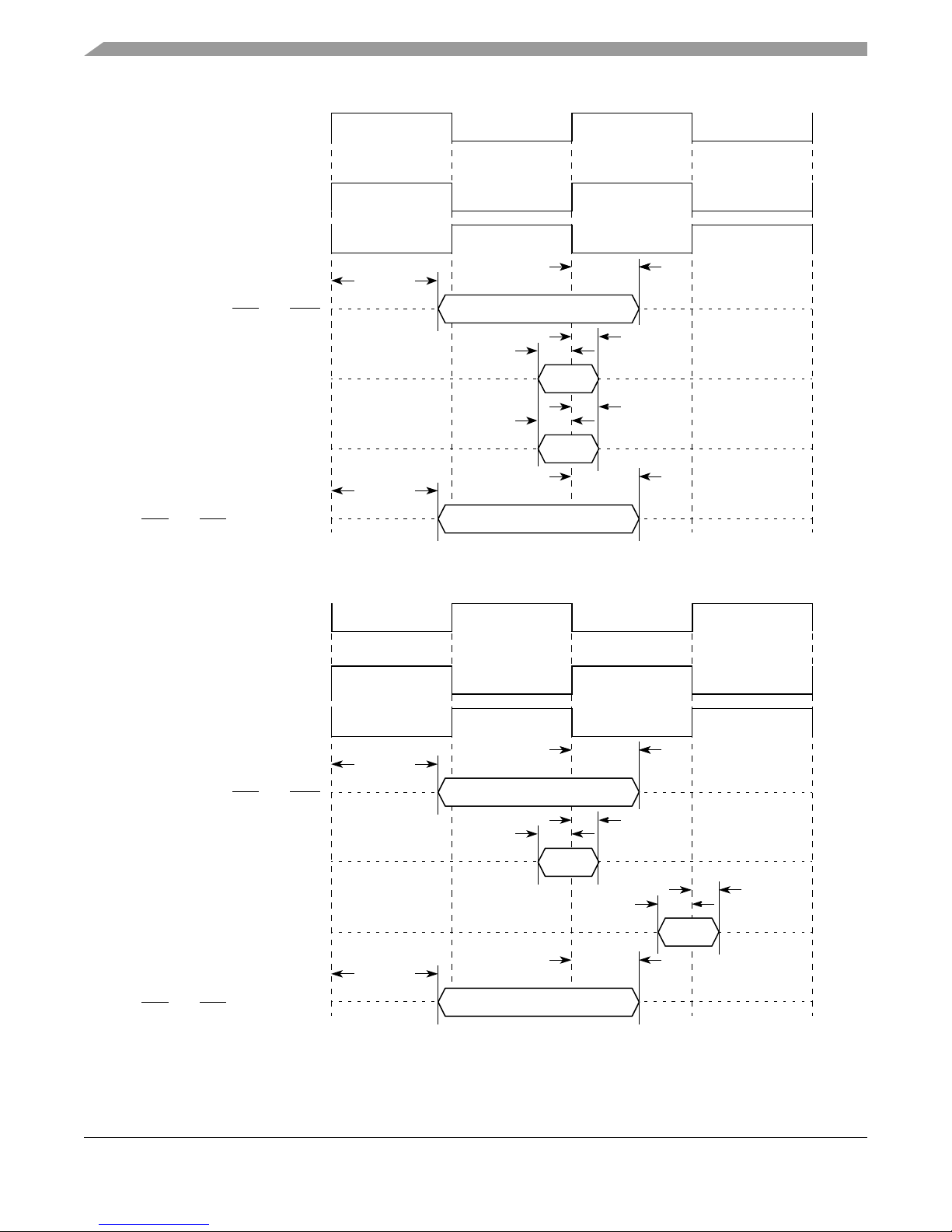
Local Bus
LSYNC_IN
UPM Mode Input Signal:
LUPWAIT
t
LBIXKH2
t
LBIVKH2
t
LBIVKH1
t
LBIXKH1
t
LBKHOZ1
T1
T3
Input Signals:
LAD[0:31]/LDP[0:3]
UPM Mode Output Signals:
LCS
[0:3]/LBS[0:3]/LGPL[0:5]
GPCM Mode Output Signals:
LCS
[0:3]/LWE
t
LBKHOV1
t
LBKHOV1
t
LBKHOZ1
LCLK
UPM Mode Input Signal:
LUPWAIT
t
LBIXKH
t
LBIVKH
t
LBIVKH
t
LBIXKH
t
LBKHOZ
T1
T3
Input Signals:
LAD[0:31]/LDP[0:3]
UPM Mode Output Signals:
LCS
[0:3]/LBS[0:3]/LGPL[0:5]
GPCM Mode Output Signals:
LCS
[0:3]/LWE
t
LBKHOV
t
LBKHOV
t
LBKHOZ
(DLL Bypass Mode)
Figure 25. Local Bus Signals, GPCM/UPM Signals for LCRR[CLKDIV] = 2 (DLL Enabled)
Figure 26. Local Bus Signals, GPCM/UPM Signals for LCRR[CLKDIV] = 2 (DLL Bypass Mode)
MPC8360E/MPC8358E PowerQUICC II Pro Processor Revision 2.x TBGA Silicon Hardware Specifications, Rev. 4
46 Freescale Semiconductor
Page 47
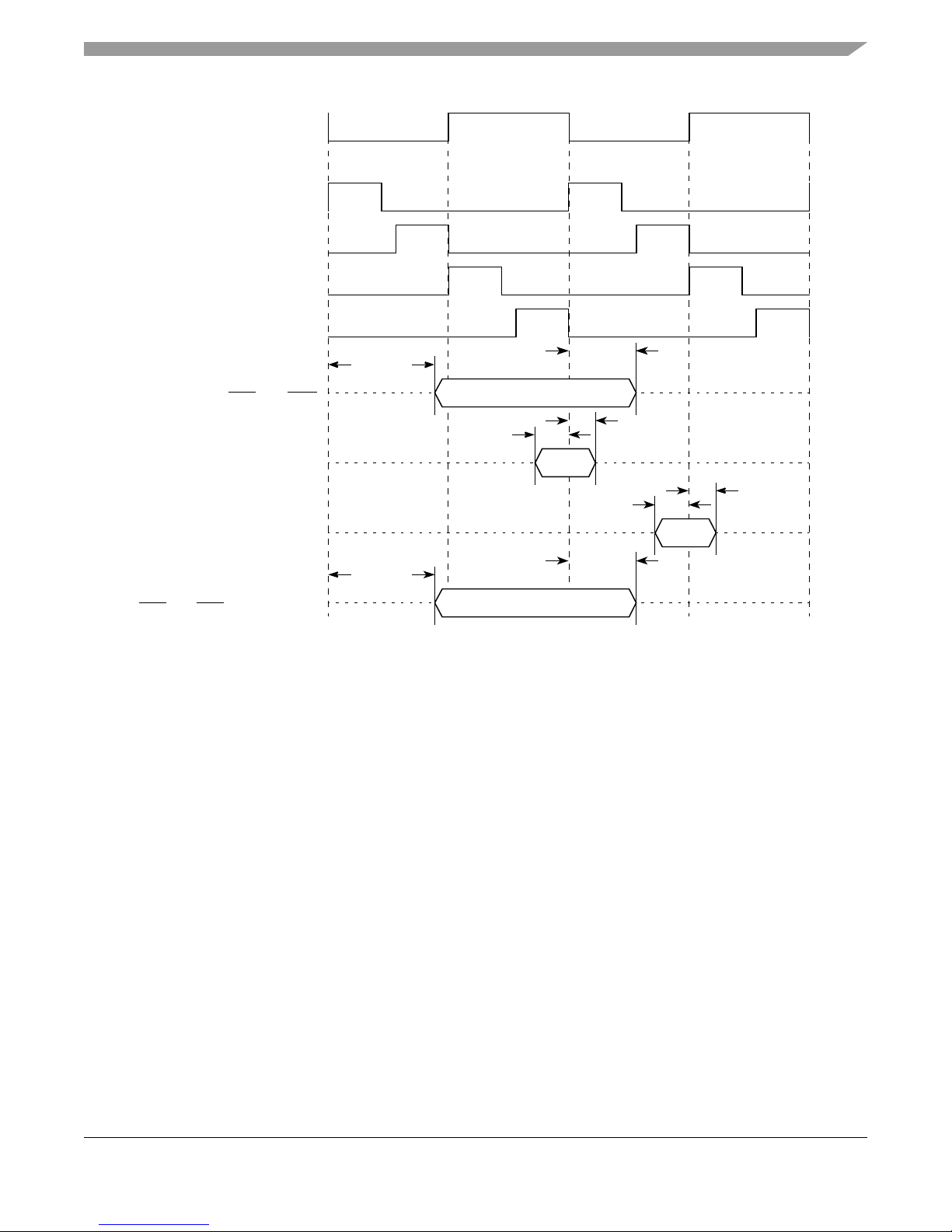
Local Bus
LCLK
UPM Mode Input Signal:
LUPWAIT
t
LBIXKH
t
LBIVKH
t
LBIVKH
t
LBIXKH
t
LBKHOZ
T1
T3
UPM Mode Output Signals:
LCS
[0:3]/LBS[0:3]/LGPL[0:5]
GPCM Mode Output Signals:
LCS
[0:3]/LWE
t
LBKHOV
t
LBKHOV
t
LBKHOZ
T2
T4
Input Signals:
LAD[0:31]/LDP[0:3]
(DLL Bypass Mode)
Figure 27. Local Bus Signals, GPCM/UPM Signals for LCRR[CLKDIV] = 4 (DLL Bypass Mode)
MPC8360E/MPC8358E PowerQUICC II Pro Processor Revision 2.x TBGA Silicon Hardware Specifications, Rev. 4
Freescale Semiconductor 47
Page 48
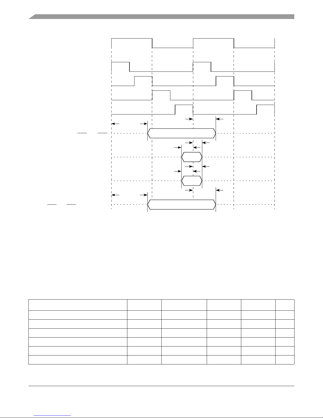
JTAG
LSYNC_IN
UPM Mode Input Signal:
LUPWAIT
t
LBIXKH2
t
LBIVKH2
t
LBIVKH1
t
LBIXKH1
t
LBKHOZ1
T1
T3
Input Signals:
LAD[0:31]/LDP[0:3]
UPM Mode Output Signals:
LCS
[0:3]/LBS[0:3]/LGPL[0:5]
GPCM Mode Output Signals:
LCS
[0:3]/LWE
t
LBKHOV1
t
LBKHOV1
t
LBKHOZ1
T2
T4
Figure 28. Local Bus Signals, GPCM/UPM Signals for LCRR[CLKDIV] = 4 (DLL Enabled)
10 JTAG
This section describes the DC and AC electrical specifications for the IEEE 1149.1 (JTAG) interface of
the MPC8360E/58E.
10.1 JTAG DC Electrical Characteristics
Table 42 provides the DC electrical characteristics for the IEEE 1149.1 (JTAG) interface of the device.
Output high voltage V
Output low voltage V
Output low voltage V
Input high voltage V
Input low voltage V
Input current I
MPC8360E/MPC8358E PowerQUICC II Pro Processor Revision 2.x TBGA Silicon Hardware Specifications, Rev. 4
48 Freescale Semiconductor
Table 42. JTAG interface DC Electrical Characteristics
Characteristic Symbol Condition Min Max Unit
OH
OL
OL
IH
IL
IN
I
= –6.0 mA 2.4 — V
OH
IOL = 6.0 mA — 0.5 V
I
= 3.2 mA — 0.4 V
OL
—2.5OV
— –0.3 0.8 V
0 V ≤ VIN ≤ OV
DD
—±10μA
+ 0.3 V
DD
Page 49
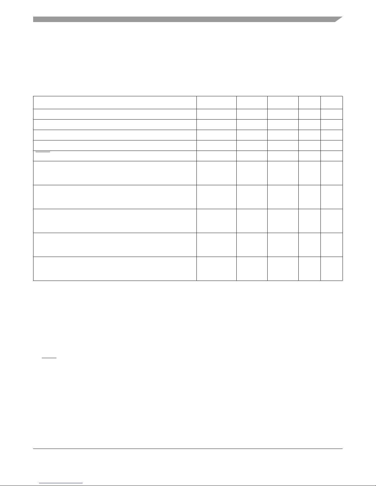
JTAG
10.2 JTAG AC Electrical Characteristics
This section describes the AC electrical specifications for the IEEE 1149.1 (JTAG) interface of the device.
Table 43 provides the JTAG AC timing specifications as defined in Figure 30 through Figure 33.
Table 43. JTAG AC Timing Specifications (Independent of CLKIN)
At recommended operating conditions (see Ta b l e 2 ).
1
JTG
JTG
& t
TRST
JTDVKH
t
JTIVKH
JTDXKH
t
JTIXKH
JTKLDV
JTKLOV
JTKLDX
JTKLOX
JTKLDZ
JTKLOZ
2
JTGF
Min Max Unit Notes
0 33.3 MHz —
30 — ns —
45 55 % —
02ns—
25 — ns 3
ns
4
4
—
—
ns
10
10
—
—
ns
2
2
11
11
ns
2
2
—
—
ns
2
2
19
9
Parameter Symbol
JTAG external clock frequency of operation f
JTAG external clock cycle time t
JTAG external clock duty cycle t
JTAG external clock rise and fall times t
TRST
assert time t
JTKHKL/tJTG
JTGR
Input setup times:
Boundary-scan data
t
TMS, TDI
Input hold times:
Boundary-scan data
t
TMS, TDI
Valid times:
Boundary-scan data
TDO
t
t
Output hold times:
Boundary-scan data
TDO
t
t
JTAG external clock to output high impedance:
Boundary-scan data
TDO
t
t
Notes:
1. All outputs are measured from the midpoint voltage of the falling/rising edge of t
to the midpoint of the signal in question.
TCLK
The output timings are measured at the pins. All output timings assume a purely resistive 50-Ω load (see Figure 22).
Time-of-flight delays must be added for trace lengths, vias, and connectors in the system.
2. The symbols used for timing specifications herein follow the pattern of t
for inputs and t
(first two letters of functional block)(reference)(state)(signal)(state)
device timing (JT) with respect to the time data input signals (D) reaching the valid state (V) relative to the t
reference (K) going to the high (H) state or setup time. Also, t
data input signals (D) went invalid (X) relative to the t
JTG
JTDXKH
clock reference (K) going to the high (H) state. Note that, in general,
(first two letters of functional block)(signal)(state) (reference)(state)
for outputs. For example, t
symbolizes JTAG
JTDVKH
JTG
clock
symbolizes JTAG timing (JT) with respect to the time
the clock reference symbol representation is based on three letters representing the clock of a particular functional. For rise
and fall times, the latter convention is used with the appropriate letter: R (rise) or F (fall).
3. TRST
4. Non-JTAG signal input timing with respect to t
5. Non-JTAG signal output timing with respect to t
is an asynchronous level sensitive signal. The setup time is for test purposes only.
.
TCLK
.
TCLK
6. Guaranteed by design and characterization.
4
4
5
5
5, 6
6
MPC8360E/MPC8358E PowerQUICC II Pro Processor Revision 2.x TBGA Silicon Hardware Specifications, Rev. 4
Freescale Semiconductor 49
Page 50
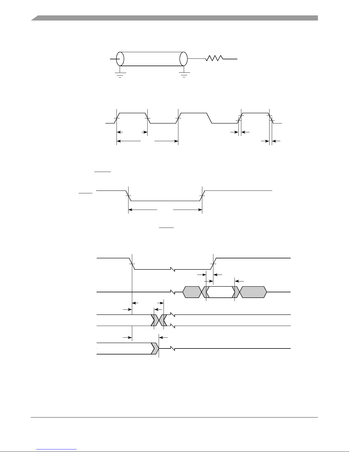
JTAG
Output
Z0 = 50 Ω
OVDD/2
R
L
= 50 Ω
JTAG
t
JTKHKL
t
JTGR
External Clock
VMVMVM
t
JTG
t
JTGF
VM = Midpoint Voltage (OVDD/2)
TRST
VM = Midpoint Voltage (OVDD/2)
VM VM
t
TRST
VM = Midpoint Voltage (OVDD/2)
VM VM
t
JTDVKH
t
JTDXKH
Boundary
Data Outputs
Boundary
Data Outputs
JTAG
External Clock
Boundary
Data Inputs
Output Data Valid
t
JTKLDX
t
JTKLDZ
t
JTKLDV
Input
Data Valid
Output Data Valid
Figure 29 provides the AC test load for TDO and the boundary-scan outputs of the device.
Figure 29. AC Test Load for the JTAG Interface
Figure 30 provides the JT AG clock input timing diagram.
Figure 30. JTAG Clock Input Timing Diagram
Figure 31 provides the TRST timing diagram.
Figure 32 provides the boundary-scan timing diagram.
MPC8360E/MPC8358E PowerQUICC II Pro Processor Revision 2.x TBGA Silicon Hardware Specifications, Rev. 4
50 Freescale Semiconductor
Figure 31. TRST Timing Diagram
Figure 32. Boundary-Scan Timing Diagram
Page 51
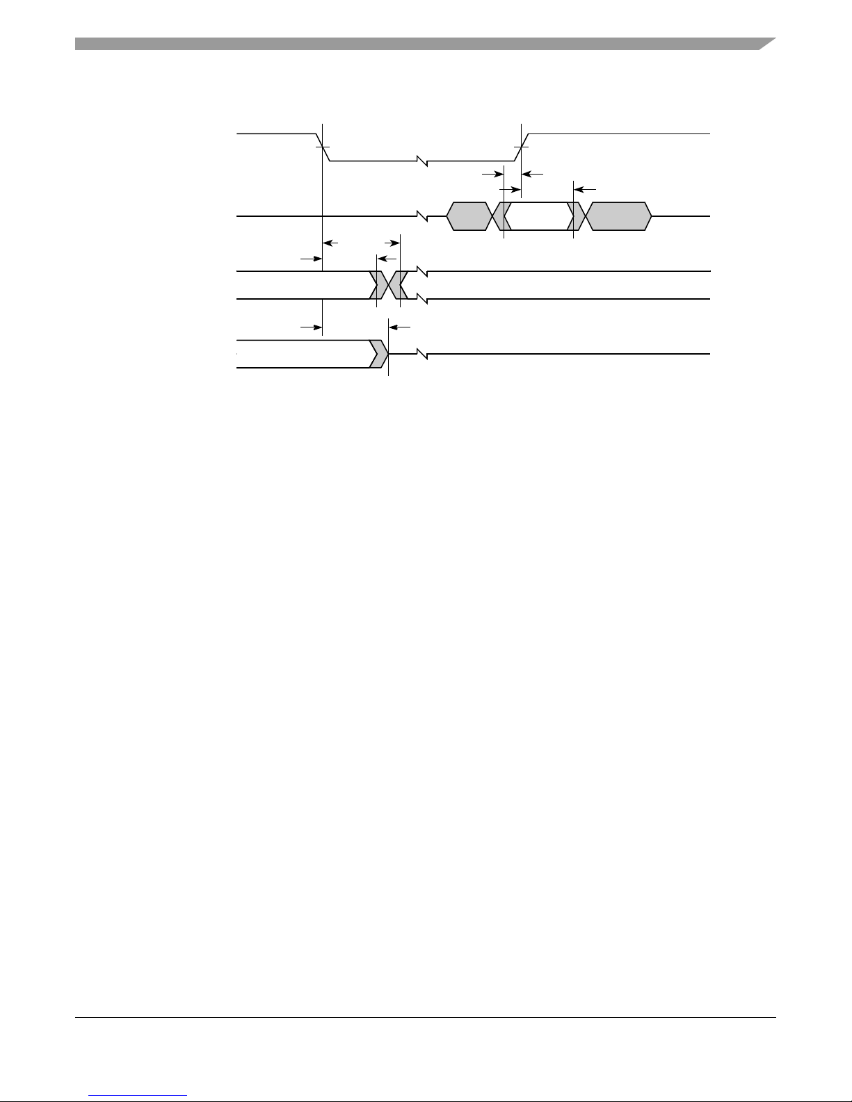
Figure 33 provides the test access port timing diagram.
VM = Midpoint Voltage (OVDD/2)
VM VM
t
JTIVKH
t
JTIXKH
JTAG
External Clock
Output Data Valid
t
JTKLOX
t
JTKLOZ
t
JTKLOV
Input
Data Valid
Output Data Valid
TDI, TMS
TDO
TDO
Figure 33. Test Access Port Timing Diagram
JTAG
MPC8360E/MPC8358E PowerQUICC II Pro Processor Revision 2.x TBGA Silicon Hardware Specifications, Rev. 4
Freescale Semiconductor 51
Page 52
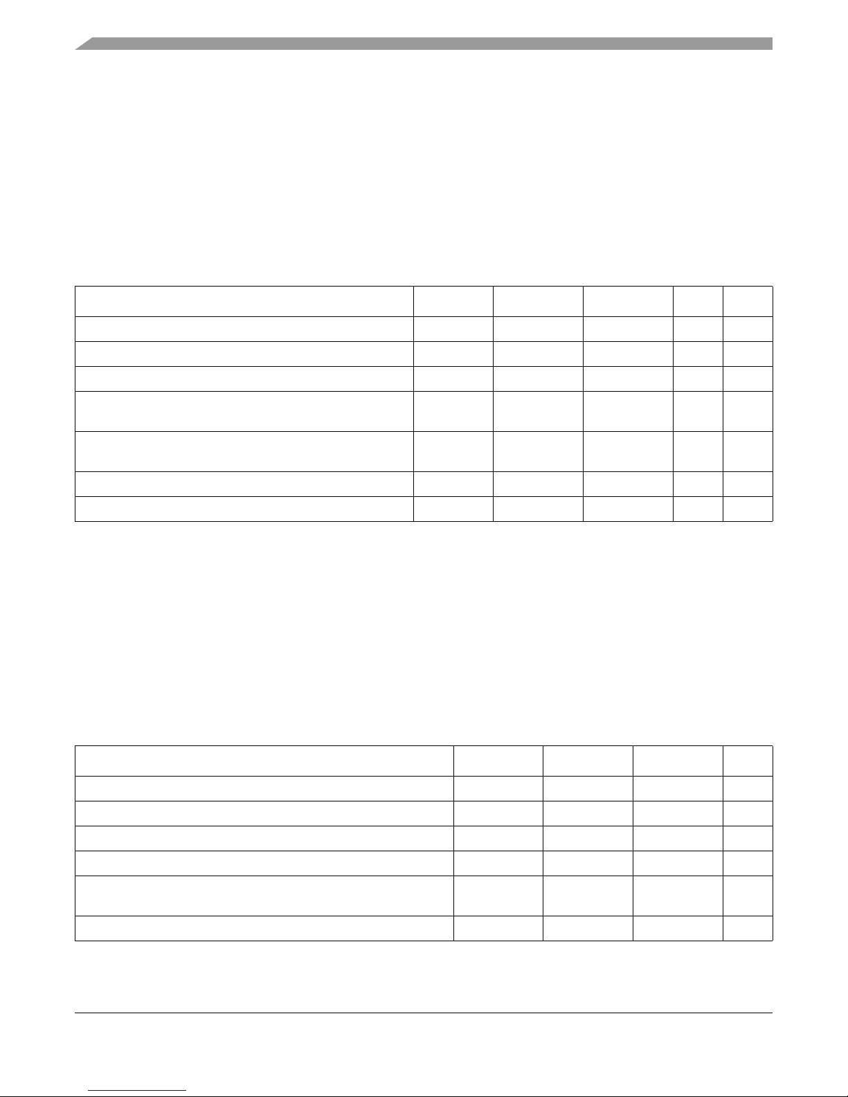
I2C
11 I2C
This section describes the DC and AC electrical characteristics for the I2C interface of the
MPC8360E/58E.
11.1 I2C DC Electrical Characteristics
Table 44 provides the DC electrical characteristics for the I2C interface of the device.
Table 44. I2C DC Electrical Characteristics
At recommended operating conditions with OVDD of 3.3 V ± 10%.
Parameter Symbol Min Max Unit Notes
Input high voltage level V
Input low voltage level V
Low level output voltage V
Output fall time from V
(min) to VIL(max) with a bus
IH
t
I2KLKV
IH
IL
OL
0.7 × OV
DD
–0.3 0.3 × OV
00.4V1
20 + 0.1 × C
B
capacitance from 10 to 400 pF
Pulse width of spikes which must be suppressed by the input
t
I2KHKL
050ns3
filter
Capacitance for each I/O pin C
Input current (0 V ≤ V
≤ OVDD)I
IN
I
IN
—10pF—
—±10μA4
Notes:
1. Output voltage (open drain or open collector) condition = 3 mA sink current.
= capacitance of one bus line in pF.
2. C
B
3. Refer to the
MPC8360E Integrated Communications Processor Family Reference Manual
for information on the digital filter
used.
4. I/O pins will obstruct the SDA and SCL lines if OV
is switched off.
DD
11.2 I2C AC Electrical Specifications
Table 45 provides the AC timing parameters for the I2C interface of the device.
Table 45. I2C AC Electrical Specifications
All values refer to V
(min) and V
IH
(max) levels (see Ta b l e 4 4 ).
IL
Parameter Symbol
1
Min Max Unit
OVDD + 0.3 V —
DD
V—
250 ns 2
SCL clock frequency f
Low period of the SCL clock t
High period of the SCL clock t
Setup time for a repeated START condition t
Hold time (repeated) START condition (after this period, the first
clock pulse is generated)
Data setup time t
MPC8360E/MPC8358E PowerQUICC II Pro Processor Revision 2.x TBGA Silicon Hardware Specifications, Rev. 4
52 Freescale Semiconductor
I2C
I2CL
I2CH
I2SVKH
t
I2SXKL
I2DVKH
0400kHz
1.3 — μs
0.6 — μs
0.6 — μs
0.6 — μs
100 — ns
Page 53
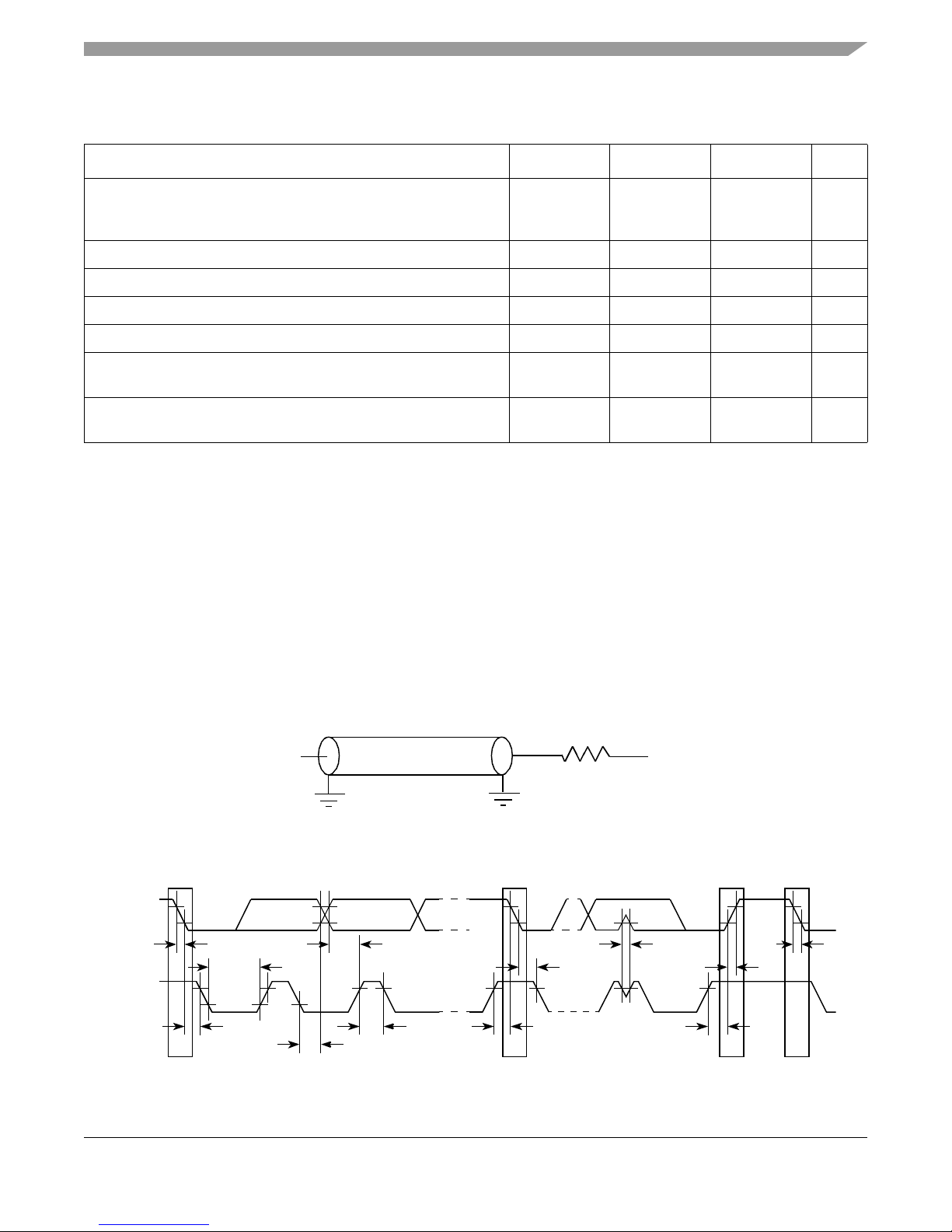
All values refer to V
Output
Z0 = 50 Ω
OVDD/2
R
L
= 50 Ω
SrS
SDA
SCL
t
I2CF
t
I2SXKL
t
I2CL
t
I2CH
t
I2DXKL
t
I2DVKH
t
I2SXKL
t
I2SVKH
t
I2KHKL
t
I2PVKH
t
I2CR
t
I2CF
PS
(min) and V
IH
Table 45. I2C AC Electrical Specifications (continued)
(max) levels (see Ta b l e 4 4 ).
IL
Parameter Symbol
1
I2C
Min Max Unit
Data hold time:
CBUS compatible masters
2
I
C bus devices
Rise time of both SDA and SCL signals t
Fall time of both SDA and SCL signals t
Set-up time for STOP condition t
Bus free time between a STOP and START condition t
Noise margin at the LOW level for each connected device (including
t
I2DXKL
I2CR
I2CF
I2PVKH
I2KHDX
V
NL
—
2
0
20 + 0.1 C
20 + 0.1 C
4
b
4
b
—
3
0.9
300 ns
300 ns
0.6 — μs
1.3 — μs
0.1 × OV
DD
—V
hysteresis)
Noise margin at the HIGH level for each connected device (including
V
NH
0.2 × OV
DD
—V
hysteresis)
Notes:
1. The symbols used for timing specifications follow the pattern of t
inputs and t
(first two letters of functional block)(reference)(state)(signal)(state)
with respect to the time data input signals (D) reach the valid state (V) relative to the t
(H) state or setup time. Also, t
(S) went invalid (X) relative to the t
symbolizes I2C timing (I2) for the time that the data with respect to the start condition
I2SXKL
clock reference (K) going to the low (L) state or hold time. Also, t
I2C
timing (I2) for the time that the data with respect to the stop condition (P) reaching the valid state (V) relative to the t
(first two letters of functional block)(signal)(state)(reference)(state)
for outputs. For example, t
clock reference (K) going to the high
I2C
symbolizes I2C timing (I2)
I2DVKH
symbolizes I2C
I2PVKH
I2C
reference (K) going to the high (H) state or setup time. For rise and fall times, the latter convention is used with the appropriate
letter: R (rise) or F (fall).
2. The device provides a hold time of at least 300 ns for the SDA signal (referred to the V
min of the SCL signal) to bridge the
IH
undefined region of the falling edge of SCL.
3. The maximum t
= capacitance of one bus line in pF.
4. C
B
has only to be met if the device does not stretch the LOW period (t
I2DVKH
) of the SCL signal.
I2CL
μs
for
clock
Figure 34 provides the AC test load for the I2C.
Figure 35 shows the AC timing diagram for the I2C bus.
MPC8360E/MPC8358E PowerQUICC II Pro Processor Revision 2.x TBGA Silicon Hardware Specifications, Rev. 4
Freescale Semiconductor 53
Figure 34. I2C AC Test Load
Figure 35. I2C Bus AC Timing Diagram
Page 54
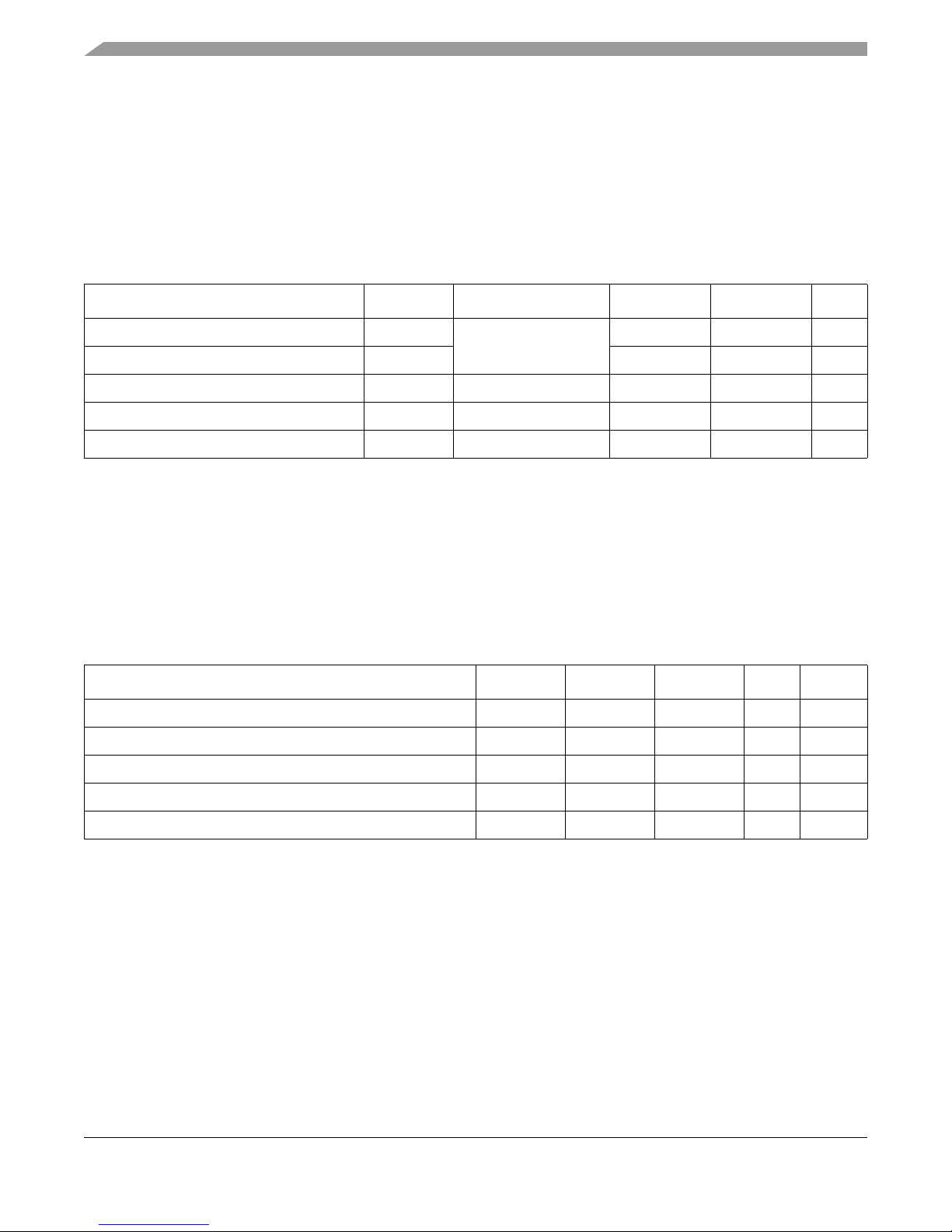
PCI
12 PCI
This section describes the DC and AC electrical specifications for the PCI bus of the MPC8360E/58E.
12.1 PCI DC Electrical Characteristics
Table 46 provides the DC electrical characteristics for the PCI interface of the device.
Table 46. PCI DC Electrical Characteristics
Parameter Symbol Test Condition Min Max Unit
High-level input voltage V
Low-level input voltage V
High-level output voltage V
Low-level output voltage V
Input current I
IH
IL
OH
OL
IN
V
≥ VOH (min) or 0.5 × OV
OUT
V
≤ VOL (max) -0.5 0.3 × OV
OUT
IOH = –500 μA0.9 × OV
OVDD + 0.5 V
DD
DD
IOL = 1500 μA—0.1 × OV
IN
1
≤ OV
DD
—±10μA
0 V ≤ V
DD
V
—V
DD
V
Note:
1. Note that the symbol V
, in this case, represents the OVIN symbol referenced in Ta bl e 1 and Ta b le 2 .
IN
12.2 PCI AC Electrical Specifications
This section describes the general AC timing parameters of the PCI bus of the device. Note that the
PCI_CLK or PCI_SYNC_IN signal is used as the PCI input clock depending on whether the device is
configured as a host or agent device. Table 47 provides the PCI AC timing specifications at 66 MHz.
.
Parameter Symbol
Clock to output valid t
Output hold from clock t
Clock to output high impedance t
Input setup to clock t
Input hold from clock t
Notes:
1. The symbols used for timing specifications follow the pattern of t
inputs and t
(first two letters of functional block)(reference)(state)(signal)(state)
(PC) with respect to the time the input signals (I) reach the valid state (V) relative to the PCI_SYNC_IN clock, t
(K) going to the high (H) state or setup time. Also, t
(R) went high (H) relative to the frame signal (F) going to the valid (V) state.
2. See the timing measurement conditions in the
3. For purposes of active/float timing measurements, the Hi-Z or off-state is defined to be when the total current delivered
through the component pin is less than or equal to the leakage current specification.
4. Input timings are measured at the pin.
5. In rev. 2.0 silicon, due to errata, t
6. In rev. 2.0 silicon, due to errata, t
Table 47. PCI AC Timing Specifications at 66 MHz
PCKHOV
PCKHOX
PCKHOZ
PCIVKH
PCIXKH
(first two letters of functional block)(signal)(state)(reference)(state)
for outputs. For example, t
symbolizes PCI timing (PC) with respect to the time hard reset
PCRHFV
PCI 2.2 Local Bus Specifications
maximum is 6.6 ns. Refer to Errata PCI21 in
PCIHOV
minimum is 1 ns. Refer to Errata PCI17 in
PCIXKH
1
Min Max Unit Notes
— 6.0 ns 2, 5
1—ns2
—14ns2, 3
3.0 — ns 2, 4
0.3 — ns 2, 4, 6
.
Chip Errata for the MPC8360E, Rev. 1
Chip Errata for the MPC8360E, Rev. 1
symbolizes PCI timing
PCIVKH
, reference
SYS
for
.
.
MPC8360E/MPC8358E PowerQUICC II Pro Processor Revision 2.x TBGA Silicon Hardware Specifications, Rev. 4
54 Freescale Semiconductor
Page 55
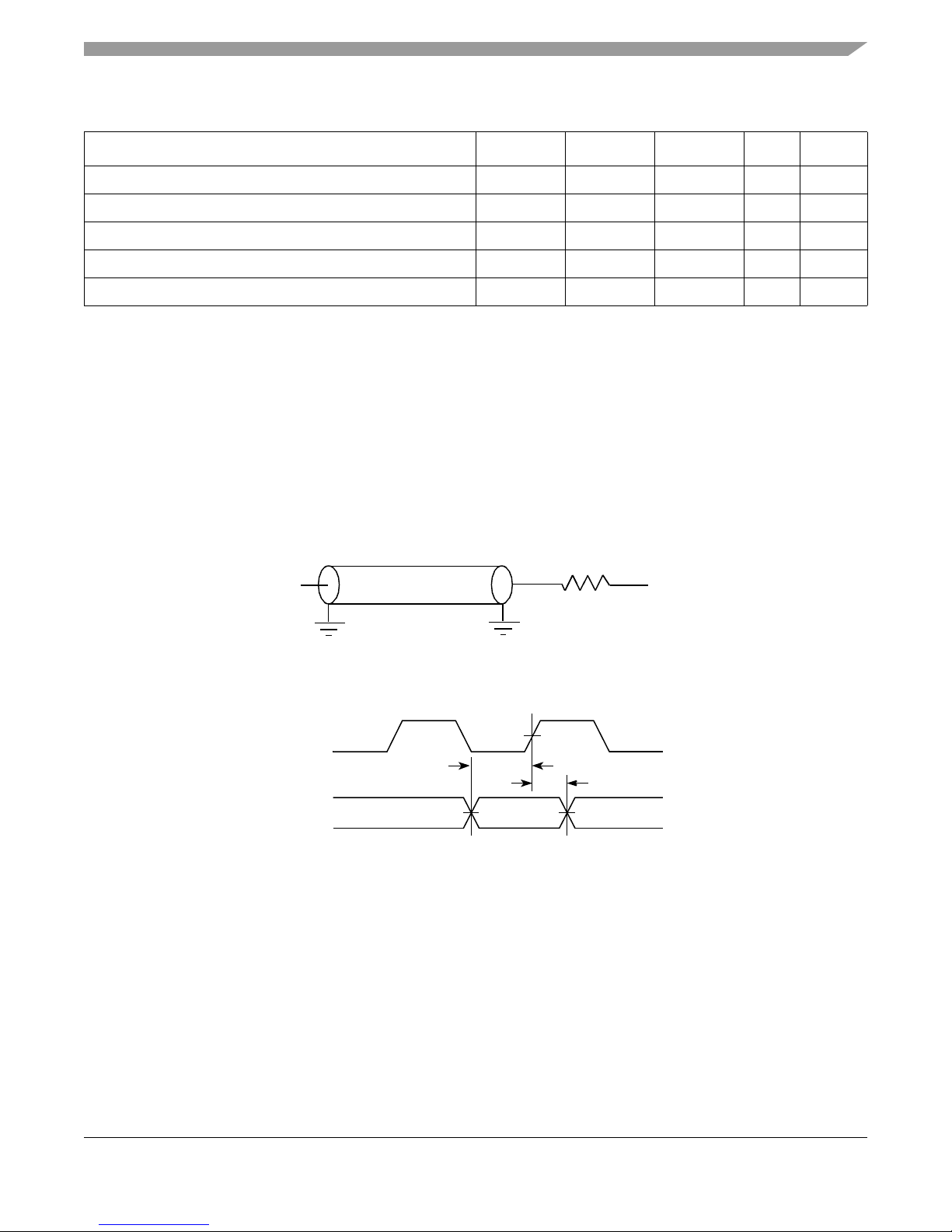
Table 48. PCI AC Timing Specifications at 33 MHz
Output
Z0 = 50 Ω
OVDD/2
R
L
= 50 Ω
t
PCIVKH
CLK
Input
t
PCIXKH
PCI
PCKHOV
PCKHOX
PCKHOZ
PCIVKH
PCIXKH
1
Min Max Unit Notes
—11ns2
2—ns2
—14ns2, 3
7.0 — ns 2, 4
0.3 — ns 2, 4, 5
Parameter Symbol
Clock to output valid t
Output hold from clock t
Clock to output high impedance t
Input setup to clock t
Input hold from clock t
Notes:
1. The symbols used for timing specifications herein follow the pattern of t
for inputs and t
(first two letters of functional block)(reference)(state)(signal)(state)
(PC) with respect to the time the input signals (I) reach the valid state (V) relative to the PCI_SYNC_IN clock, t
(K) going to the high (H) state or setup time. Also, t
symbolizes PCI timing (PC) with respect to the time hard reset
PCRHFV
(first two letters of functional block)(signal)(state)(reference)(state)
for outputs. For example, t
symbolizes PCI timing
PCIVKH
, reference
SYS
(R) went high (H) relative to the frame signal (F) going to the valid (V) state.
2. See the timing measurement conditions in the
PCI 2.2 Local Bus Specifications
.
3. For purposes of active/float timing measurements, the Hi-Z or off-state is defined to be when the total current delivered
through the component pin is less than or equal to the leakage current specification.
4. Input timings are measured at the pin.
5. In rev. 2.0 silicon, due to errata, t
minimum is 1 ns. Refer to Errata PCI17 in
PCIXKH
Chip Errata for the MPC8360E, Rev. 1
Figure 36 provides the AC test load for PCI.
.
Figure 36. PCI AC Test Load
Figure 37 shows the PCI input AC timing conditions.
Figure 37. PCI Input AC Timing Measurement Conditions
MPC8360E/MPC8358E PowerQUICC II Pro Processor Revision 2.x TBGA Silicon Hardware Specifications, Rev. 4
Freescale Semiconductor 55
Page 56
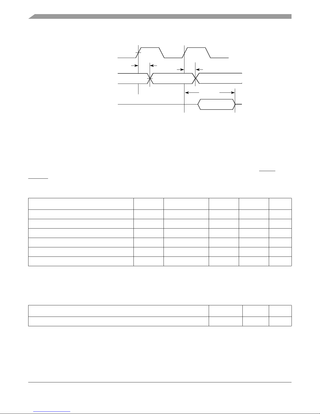
Timers
CLK
Output Delay
t
PCKHOV
High-Impedance
t
PCKHOZ
Output
t
PCKHOX
Figure 38 shows the PCI output AC timing conditions.
Figure 38. PCI Output AC Timing Measurement Condition
13 Timers
This section describes the DC and AC electrical specifications for the timers of the MPC8360E/58E.
13.1 Timers DC Electrical Characteristics
Table 49 provides the DC electrical characteristics for the device timer pins, including TIN, TOUT ,
TGATE, and RTC_CLK.
Table 49. Timers DC Electrical Characteristics
Characteristic Symbol Condition Min Max Unit
Output high voltage V
Output low voltage V
Output low voltage V
Input high voltage V
Input low voltage V
Input current I
OH
OL
OL
IH
IL
IN
I
= –6.0 mA 2.4 — V
OH
IOL = 6.0 mA — 0.5 V
IOL = 3.2 mA — 0.4 V
—2.0OV
— –0.3 0.8 V
0 V ≤ VIN ≤ OV
DD
—±10μA
+ 0.3 V
DD
13.2 Timers AC Timing Specifications
Table 50 provides the timer input and output AC timing specifications.
Table 50. Timers Input AC Timing Specifications
Characteristic Symbol
Timers inputs—minimum pulse width t
Notes:
1. Input specifications are measured from the 50% level of the signal to the 50% level of the rising edge of CLKIN. Timings are
measured at the pin.
2. Timers inputs and outputs are asynchronous to any visible clock. Timers outputs should be synchronized before use by any
external synchronous logic. Timers inputs are required to be valid for at least t
TIWID
1
2
TIWID
ns to ensure proper operation.
Typ U nit
20 ns
MPC8360E/MPC8358E PowerQUICC II Pro Processor Revision 2.x TBGA Silicon Hardware Specifications, Rev. 4
56 Freescale Semiconductor
Page 57
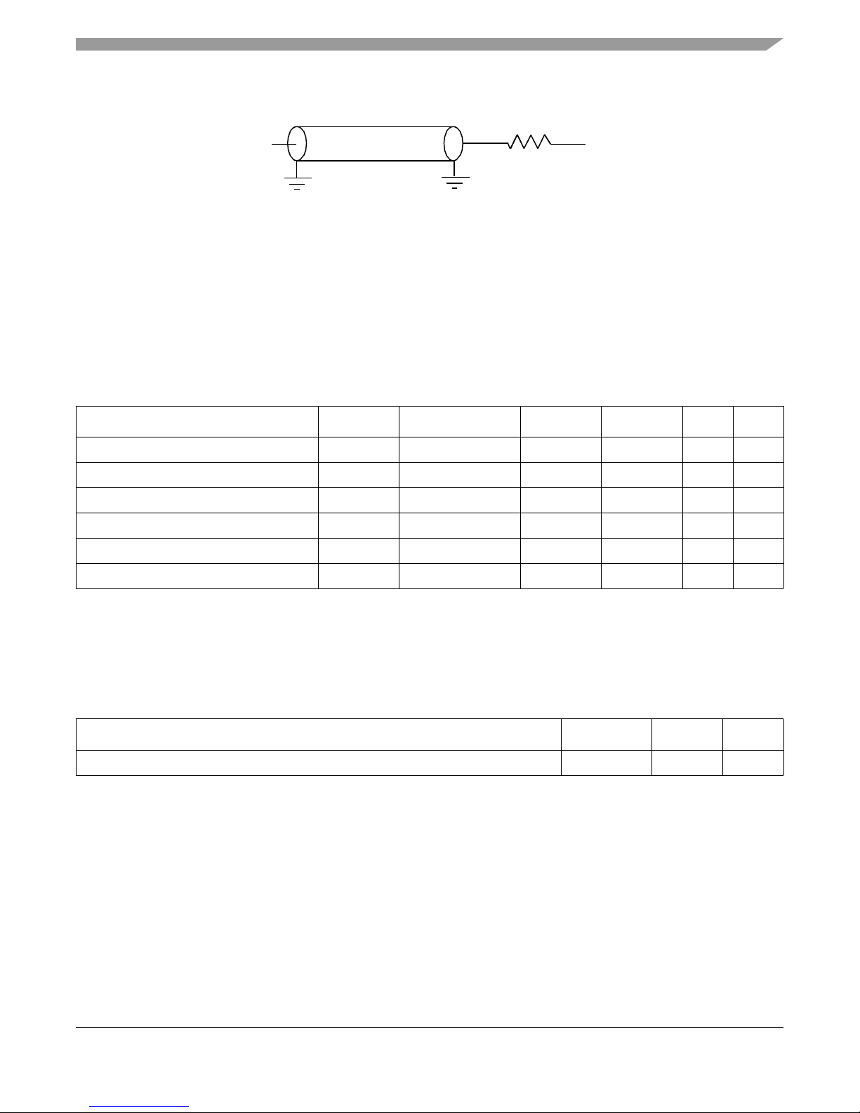
Figure 39 provides the AC test load for the timers.
Output
Z0 = 50 Ω
OVDD/2
R
L
= 50 Ω
Figure 39. Timers AC Test Load
14 GPIO
This section describes the DC and AC electrical specifications for the GPIO of the MPC8360E/58E.
14.1 GPIO DC Electrical Characteristics
Table 51 provides the DC electrical characteristics for the device GPIO.
Table 51. GPIO DC Electrical Characteristics
Characteristic Symbol Condition Min Max Unit Notes
I
Output high voltage V
Output low voltage V
Output low voltage V
Input high voltage V
Input low voltage V
Input current I
Note: This specification applies when operating from 3.3-V supply.
OH
OL
OL
IH
IL
IN
= –6.0 mA 2.4 — V 1
OH
IOL = 6.0 mA — 0.5 V 1
I
= 3.2 mA — 0.4 V 1
OL
—2.0OV
— –0.3 0.8 V —
0 V ≤ VIN ≤ OV
DD
—±10μA—
+ 0.3 V 1
DD
GPIO
14.2 GPIO AC Timing Specifications
Table 52 provides the GPIO input and output AC timing specifications.
Table 52. GPIO Input AC Timing Specifications
Characteristic Symbol
GPIO inputs—minimum pulse width t
Notes:
1. Input specifications are measured from the 50% level of the signal to the 50% level of the rising edge of CLKIN. Timings are
measured at the pin.
2. GPIO inputs and outputs are asynchronous to any visible clock. GPIO outputs should be synchronized before use by any
external synchronous logic. GPIO inputs are required to be valid for at least t
MPC8360E/MPC8358E PowerQUICC II Pro Processor Revision 2.x TBGA Silicon Hardware Specifications, Rev. 4
Freescale Semiconductor 57
1
2
PIWID
ns to ensure proper operation.
PIWID
Typ U nit
20 ns
Page 58
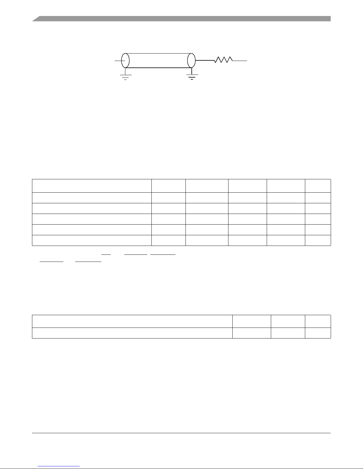
IPIC
Output
Z0 = 50 Ω
OVDD/2
R
L
= 50 Ω
Figure 40 provides the AC test load for the GPIO.
Figure 40. GPIO AC Test Load
15 IPIC
This section describes the DC and AC electrical specifications for the external interrupt pins of the
MPC8360E/58E.
15.1 IPIC DC Electrical Characteristics
Table 53 provides the DC electrical characteristics for the external interrupt pins of the IPIC.
Table 53. IPIC DC Electrical Characteristics
Characteristic Symbol Condition Min Max Unit
Input high voltage V
Input low voltage V
Input current I
Output low voltage V
Output low voltage V
Notes:
1. This table applies for pins IRQ
2. IRQ_OUT
and MCP_OUT are open drain pins, thus VOH is not relevant for those pins.
[0:7], IRQ_OUT, MCP_OUT, and CE ports Interrupts.
IH
IL
IN
OL
OL
—2.0OV
— –0.3 0.8 V
——±10μA
IOL = 6.0 mA — 0.5 V
IOL = 3.2 mA — 0.4 V
+ 0.3 V
DD
15.2 IPIC AC Timing Specifications
Table 54 provides the IPIC input and output AC timing specifications.
Table 54. IPIC Input AC Timing Specifications
Characteristic Symbol
IPIC inputs—minimum pulse width t
Notes:
1. Input specifications are measured from the 50% level of the signal to the 50% level of the rising edge of CLKIN. Timings are
measured at the pin.
2. IPIC inputs and outputs are asynchronous to any visible clock. IPIC outputs should be synchronized before use by any
external synchronous logic. IPIC inputs are required to be valid for at least t
in edge triggered mode.
PIWID
1
2
PIWID
ns to ensure proper operation when working
Min Unit
20 ns
16 SPI
This section describes the DC and AC electrical specificat ions for the SPI of the M PC8360E/58E.
MPC8360E/MPC8358E PowerQUICC II Pro Processor Revision 2.x TBGA Silicon Hardware Specifications, Rev. 4
58 Freescale Semiconductor
Page 59
16.1 SPI DC Electrical Characteristics
Output
Z0 = 50 Ω
OVDD/2
R
L
= 50 Ω
Table 55 provides the DC electrical characteristics for the device SPI.
Table 55. SPI DC Electrical Characteristics
Characteristic Symbol Condition Min Max Unit
SPI
Output high voltage V
Output low voltage V
Output low voltage V
Input high voltage V
Input low voltage V
Input current I
OH
OL
OL
IH
IL
IN
I
= –6.0 mA 2.4 — V
OH
IOL = 6.0 mA — 0.5 V
I
= 3.2 mA — 0.4 V
OL
—2.0OV
+ 0.3 V
DD
— –0.3 0.8 V
0 V ≤ VIN ≤ OV
DD
—±10μA
16.2 SPI AC Timing Specifications
Table 56 and provide the SPI input and output AC timing specifications.
NIKHOX
NIKHOV
NEKHOX
NEKHOV
NIIVKH
NIIXKH
NEIVKH
NEIXKH
1
2
Min Max Unit
0.3
—
2
—
—
—
ns
8
ns
8
8—ns
0—ns
4—ns
2—ns
for
symbolizes the NMSI
NIKHOV
Table 56. SPI AC Timing Specifications
Characteristic Symbol
SPI outputs—Master mode (internal clock) delay t
t
SPI outputs—Slave mode (external clock) delay t
t
SPI inputs—Master mode (internal clock) input setup time t
SPI inputs—Master mode (internal clock) input hold time t
SPI inputs—Slave mode (external clock) input setup time t
SPI inputs—Slave mode (external clock) input hold time t
Notes:
1. Output specifications are measured from the 50% level of the rising edge of CLKIN to the 50% level of the signal. Timings
are measured at the pin.
2. The symbols used for timing specifications follow the pattern of t
inputs and t
outputs internal timing (NI) for the time t
(first two letters of functional block)(reference)(state)(signal)(state)
memory clock reference (K) goes from the high state (H) until outputs (O) are
SPI
valid (V).
(first two letters of functional block)(signal)(state)(reference)(state)
for outputs. For example, t
Figure 41 provides the AC test load for the SPI.
MPC8360E/MPC8358E PowerQUICC II Pro Processor Revision 2.x TBGA Silicon Hardware Specifications, Rev. 4
Freescale Semiconductor 59
Figure 41. SPI AC Test Load
Page 60
TDM/SI
SPICLK (Input)
t
NEIXKH
t
NEIVKH
t
NEKHOV
Input Signals:
SPIMOSI
(See Note)
Output Signals:
SPIMISO
(See Note)
Note: The clock edge is selectable on SPI.
SPICLK (Output)
t
NIIXKH
t
NIKHOV
Input Signals:
SPIMISO
(See Note)
Output Signals:
SPIMOSI
(See Note)
Note: The clock edge is selectable on SPI.
t
NIIVKH
Figure 42 and Figure 43 represent the AC timing from Table 56. Note that although the specifications
generally reference the rising edge of the clock, these AC timing diagrams also apply when the falling edge
is the active edge.
Figure 42 shows the SPI timing in slave mode (external clock).
Figure 42. SPI AC Timing in Slave Mode (External Clock) Diagram
Figure 43 shows the SPI timing in Master mode (internal clock).
Figure 43. SPI AC Timing in Master Mode (Internal Clock) Diagram
17 TDM/SI
This section describes the DC and AC electrical specifications for the time-division-multiplexed and serial
interface of the MPC8360E/58E.
17.1 TDM/SI DC Electrical Characteristics
Table 57 provides the DC electrical characteristics for the device TDM/SI.
Table 57. TDM/SI DC Electrical Characteristics
Characteristic Symbol Condition Min Max Unit
Output high voltage V
Output low voltage V
Input high voltage V
60 Freescale Semiconductor
MPC8360E/MPC8358E PowerQUICC II Pro Processor Revision 2.x TBGA Silicon Hardware Specifications, Rev. 4
OH
OL
IH
I
= –2.0 mA 2.4 — V
OH
IOL = 3.2 mA — 0.5 V
—2.0OV
+ 0.3 V
DD
Page 61
TDM/SI
Output
Z0 = 50 Ω
OVDD/2
R
L
= 50 Ω
Table 57. TDM/SI DC Electrical Characteristics (continued)
Characteristic Symbol Condition Min Max Unit
Input low voltage V
Input current I
IL
IN
0 V ≤ VIN ≤ OV
— –0.3 0.8 V
DD
—±10μA
17.2 TDM/SI AC Timing Specifications
Table 58 provides the TDM/SI input and output AC timing specifications.
Table 58. TDM/SI AC Timing Specifications
Characteristic Symbol
TDM/SI outputs—External clock delay t
TDM/SI outputs—External clock high impedance t
TDM/SI inputs—External clock input setup time t
TDM/SI inputs—External clock input hold time t
Notes:
1. Output specifications are measured from the 50% level of the rising edge of CLKIN to the 50% level of the signal. Timings
are measured at the pin.
2. The symbols used for timing specifications follow the pattern of t
inputs and t
outputs external timing (SE) for the time t
(first two letters of functional block)(reference)(state)(signal)(state)
memory clock reference (K) goes from the high state (H) until outputs (O)
TDM/SI
(first two letters of functional block)(signal)(state)(reference)(state)
for outputs. For example, t
are invalid (X).
3. Timings are measured from the positive or negative edge of the clock, according to SIxMR [CE] and SITXCEI[TXCEIx]. See
the
MPC8360E Integrated Communications Processor Family Reference Manual
SEKHOV
SEKHOX
SEIVKH
SEIXKH
1
2
Min Max
210ns
210ns
5—ns
2—ns
SEKHOX
for more details.
3
Unit
for
symbolizes the TDM/SI
Figure 44 provides the AC test load for the TDM/SI.
Figure 44. TDM/SI AC Test Load
Figure 45 represents the AC timing from Table 56. Note that although the specifications generally
reference the rising edge of the clock, these AC timing diagrams also apply when the falling edge is the
active edge.
MPC8360E/MPC8358E PowerQUICC II Pro Processor Revision 2.x TBGA Silicon Hardware Specifications, Rev. 4
Freescale Semiconductor 61
Page 62
UTOPIA/POS
TDM/SICLK (Input)
t
SEIXKH
t
SEIVKH
t
SEKHOV
Input Signals:
TDM/SI
(See Note)
Output Signals:
TDM/SI
(See Note)
t
SEKHOX
Note: The clock edge is selectable on TDM/SI
Figure 45 shows the TDM/SI timing with external clock.
Figure 45. TDM/SI AC Timing (External Clock) Diagram
18 UTOPIA/POS
This section describes the DC and AC electrical specifications for the UTOPIA/POS of the
MPC8360E/58E.
18.1 UTOPIA/POS DC Electrical Characteristics
Table 59 provides the DC electrical characteristics for the device UTOPIA.
Table 59. UTOPIA DC Electrical Characteristics
Characteristic Symbol Condition Min Max Unit
Output high voltage V
Output low voltage V
Input high voltage V
Input low voltage V
Input current I
18.2 UTOPIA/POS AC Timing Specifications
Table 60 provides the UTOPIA input and output AC timing specifications.
Table 60. UTOPIA AC Timing Specifications
Characteristic Symbol
UTOPIA outputs—Internal clock delay t
UTOPIA outputs—External clock delay t
UTOPIA outputs—Internal clock high impedance t
UTOPIA outputs—External clock high impedance t
MPC8360E/MPC8358E PowerQUICC II Pro Processor Revision 2.x TBGA Silicon Hardware Specifications, Rev. 4
62 Freescale Semiconductor
OH
OL
IH
IL
IN
I
= –8.0 mA 2.4 — V
OH
IOL = 8.0 mA — 0.5 V
—2.0OV
— –0.3 0.8 V
0 V ≤ VIN ≤ OV
UIKHOV
UEKHOV
UIKHOX
UEKHOX
DD
2
—±10μA
1
Min Max Unit Notes
0 11.5 ns —
1 11.6 ns —
08.0ns—
1 10.0 ns —
+ 0.3 V
DD
Page 63
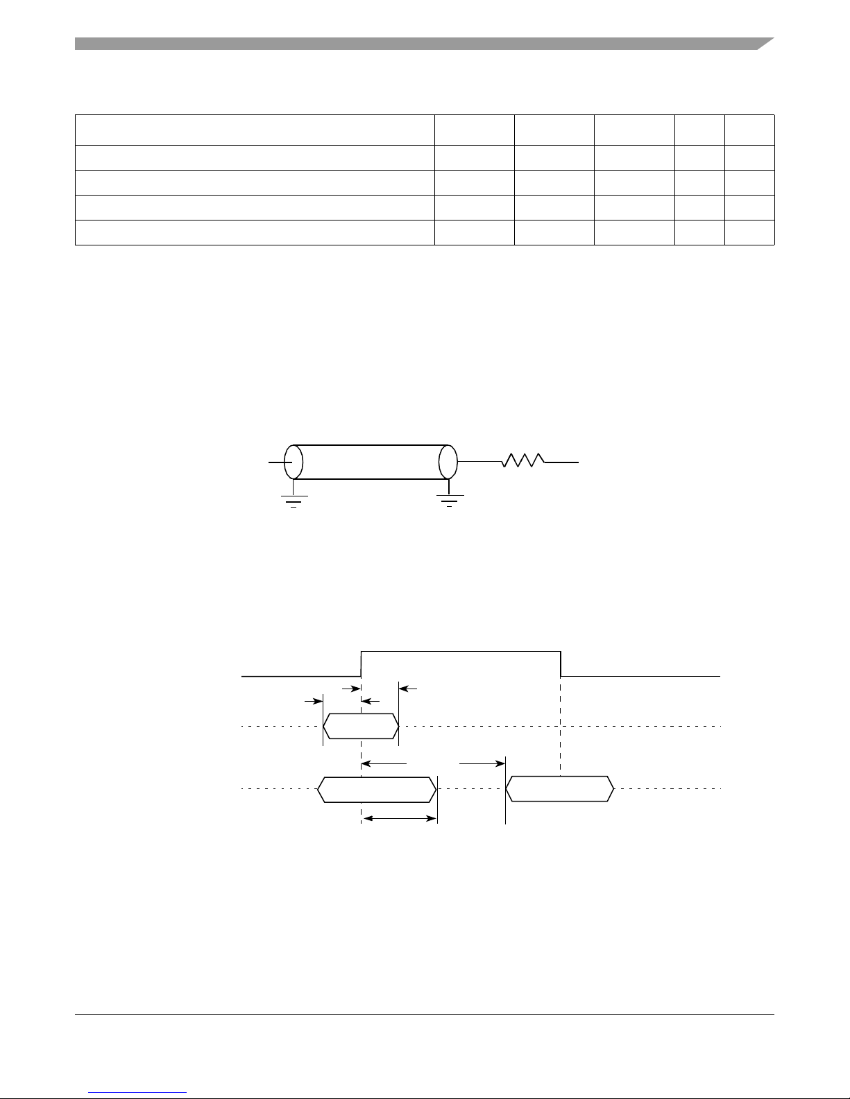
Table 60. UTOPIA AC Timing Specifications1 (continued)
Output
Z0 = 50 Ω
OVDD/2
R
L
= 50 Ω
UtopiaCLK (Input)
t
UEIXKH
t
UEIVKH
t
UEKHOV
Input Signals:
UTOPIA
Output Signals:
UTOPIA
t
UEKHOX
UTOPIA/POS
UIIVKH
UEIVKH
UIIXKH
UEIXKH
2
Min Max Unit Notes
6—ns—
4—ns3
2.4 — ns —
1—ns3
Characteristic Symbol
UTOPIA inputs—Internal clock input setup time t
UTOPIA inputs—External clock input setup time t
UTOPIA inputs—Internal clock input hold time t
UTOPIA inputs—External clock input hold time t
Notes:
1. Output specifications are measured from the 50% level of the rising edge of CLKIN to the 50% level of the signal. Timings
are measured at the pin.
2. The symbols used for timing specifications follow the pattern of t
inputs and t
outputs internal timing (UI) for the time t
(first two letters of functional block)(reference)(state)(signal)(state)
memory clock reference (K) goes from the high state (H) until outputs (O) are
UTOPIA
(first two letters of functional block)(signal)(state)(reference)(state)
for outputs. For example, t
symbolizes the UTOPIA
UIKHOX
for
invalid (X).
3. In rev. 2.0 silicon, due to errata, t
Errata QE_UPC3 in
Chip Errata for the MPC8360E, Rev. 1
minimum is 4.3 ns and t
UEIVKH
.
minimum is 1.4 ns under specific conditions. Refer to
UEIXKH
Figure 46 provides the AC test load for the UTOPIA.
Figure 46. UTOPIA AC Test Load
Figure 47 and Figure 48 represent the AC timing from Table 56. Note that although the specifications
generally reference the rising edge of the clock, these AC timing diagrams also apply when the falling edge
is the active edge.
Figure 47 shows the UTOPIA timing with external clock.
Figure 47. UTOPIA AC Timing (External Clock) Diagram
MPC8360E/MPC8358E PowerQUICC II Pro Processor Revision 2.x TBGA Silicon Hardware Specifications, Rev. 4
Freescale Semiconductor 63
Page 64
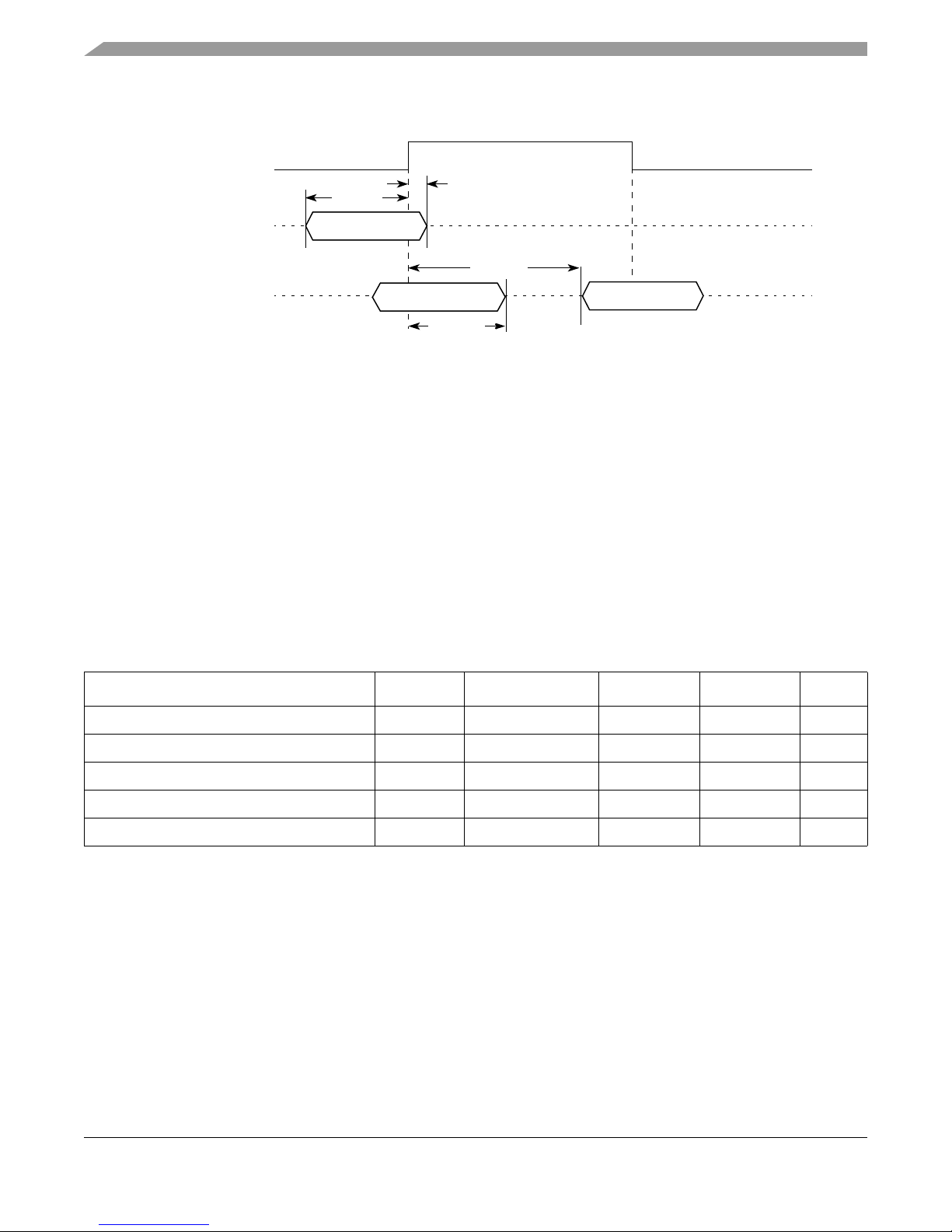
HDLC, BISYNC, Transparent, and Synchronous UART
UtopiaCLK (Output)
t
UIIXKH
t
UIKHOV
Input Signals:
UTOPIA
Output Signals:
UTOPIA
t
UIIVKH
t
UIKHOX
Figure 48 shows the UTOPIA timing with internal clock.
Figure 48. UTOPIA AC Timing (Internal Clock) Diagram
19 HDLC, BISYNC, Transparent, and Synchronous
UART
This section describes the DC and AC electrical specifications for the high level data link control (HDLC),
BISYNC, transparent, and synchronous UART protocols of the MPC8360E/58E.
19.1 HDLC, BISYNC, Transparent, and Synchronous UART DC
Electrical Characteristics
Table 61 provides the DC electrical characteristics for the device HDLC, BISYNC, transparent, and
synchronous UART protocols.
Table 61. HDLC, BISYNC, Transparent, and Synchronous UART DC Electrical Characteristics
Characteristic Symbol Condition Min Max Unit
I
Output high voltage V
Output low voltage V
Input high voltage V
Input low voltage V
Input current I
OH
OL
IH
IL
IN
= –2.0 mA 2.4 — V
OH
IOL = 3.2 mA — 0.5 V
—2.0OV
— –0.3 0.8 V
0 V ≤ VIN ≤ OV
DD
—±10μA
+ 0.3 V
DD
MPC8360E/MPC8358E PowerQUICC II Pro Processor Revision 2.x TBGA Silicon Hardware Specifications, Rev. 4
64 Freescale Semiconductor
Page 65
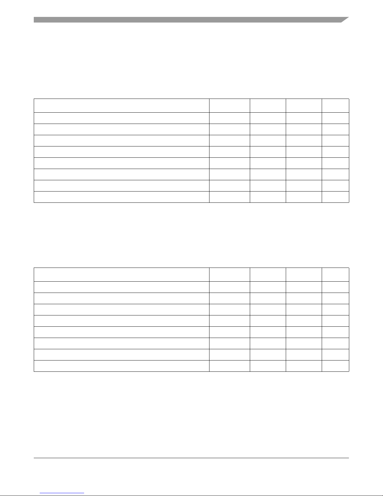
HDLC, BISYNC, Transparent, and Synchronous UART
19.2 HDLC, BISYNC, Transparent, and Synchronous UART AC Timing
Specifications
Table 62 and Table 63 provide the input and output AC timing specifications for HDLC, BISYNC,
transparent, and synchronous UART protocols.
Table 62. HDLC, BISYNC, and Transparent AC Timing Specifications
1
HIKHOV
HEKHOV
HIKHOX
HEKHOX
HIIVKH
HEIVKH
HIIXKH
HEIXKH
2
Min Max Unit
0 11.2 ns
1 10.8 ns
-0.5 5.5 ns
18ns
8.5 — ns
4—ns
1.4 — ns
1—ns
Characteristic Symbol
Outputs—Internal clock delay t
Outputs—External clock delay t
Outputs—Internal clock high impedance t
Outputs—External clock high impedance t
Inputs—Internal clock input setup time t
Inputs—External clock input setup time t
Inputs—Internal clock input hold time t
Inputs—External clock input hold time t
Notes:
1. Output specifications are measured from the 50% level of the rising edge of CLKIN to the 50% level of the signal. Timings
are measured at the pin.
2. The symbols used for timing specifications follow the pattern of t
inputs and t
internal timing (HI) for the time t
(first two letters of functional block)(reference)(state)(signal)(state)
memory clock reference (K) goes from the high state (H) until outputs (O) are invalid (X).
serial
Table 63. Synchronous UART AC Timing Specifications
Characteristic Symbol
(first two letters of functional block)(signal)(state)(reference)(state)
for outputs. For example, t
2
Min Max Unit
symbolizes the outputs
HIKHOX
1
for
Outputs—Internal clock delay t
Outputs—External clock delay t
Outputs—Internal clock high impedance t
Outputs—External clock high impedance t
Inputs—Internal clock input setup time t
Inputs—External clock input setup time t
Inputs—Internal clock input hold time t
Inputs—External clock input hold time t
UAI KHOV
UAEKHOV
UAIKHOX
UAEKHOX
UAIIVKH
UAEIVKH
UAIIXKH
UAEIXKH
0 11.3 ns
114ns
011ns
114ns
6—ns
8—ns
1—ns
1—ns
Notes:
1. Output specifications are measured from the 50% level of the rising edge of CLKIN to the 50% level of the signal. Timings
are measured at the pin.
2. The symbols used for timing specifications follow the pattern of t
inputs and t
internal timing (HI) for the time t
(first two letters of functional block)(reference)(state)(signal)(state)
memory clock reference (K) goes from the high state (H) until outputs (O) are invalid (X).
serial
(first two letters of functional block)(signal)(state)(reference)(state)
for outputs. For example, t
symbolizes the outputs
HIKHOX
for
MPC8360E/MPC8358E PowerQUICC II Pro Processor Revision 2.x TBGA Silicon Hardware Specifications, Rev. 4
Freescale Semiconductor 65
Page 66
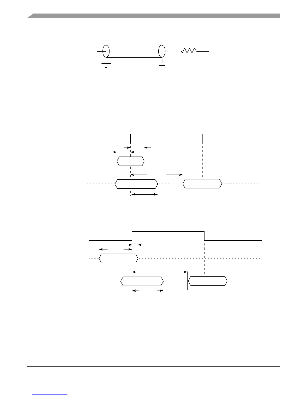
HDLC, BISYNC, Transparent, and Synchronous UART
Output
Z0 = 50 Ω
OVDD/2
R
L
= 50 Ω
Serial CLK (Input)
t
HEIXKH
t
HEIVKH
t
HEKHOV
Input Signals:
(See Note)
Output Signals:
(See Note)
t
HEKHOX
Note: The clock edge is selectable.
Serial CLK (Output)
t
HIIXKH
tHIKHOV
Input Signals:
(See Note)
t
HIIVKH
t
HIKHOX
Note: The clock edge is selectable.
Output Signals:
(See Note)
Figure 49 provides the AC test load.
Figure 49. AC Test Load
19.3 AC Test Load
Figure 50 and Figure 51 represent the AC timing from Table 62 and Table 63. Note that although the
specifications generally reference the rising edge of the clock, these AC timing diagrams also apply when
the falling edge is the active edge.
Figure 50 shows the timing with external clock.
Figure 50. AC Timing (External Clock) Diagram
Figure 51 shows the timing with internal clock.
Figure 51. AC Timing (Internal Clock) Diagram
MPC8360E/MPC8358E PowerQUICC II Pro Processor Revision 2.x TBGA Silicon Hardware Specifications, Rev. 4
66 Freescale Semiconductor
Page 67
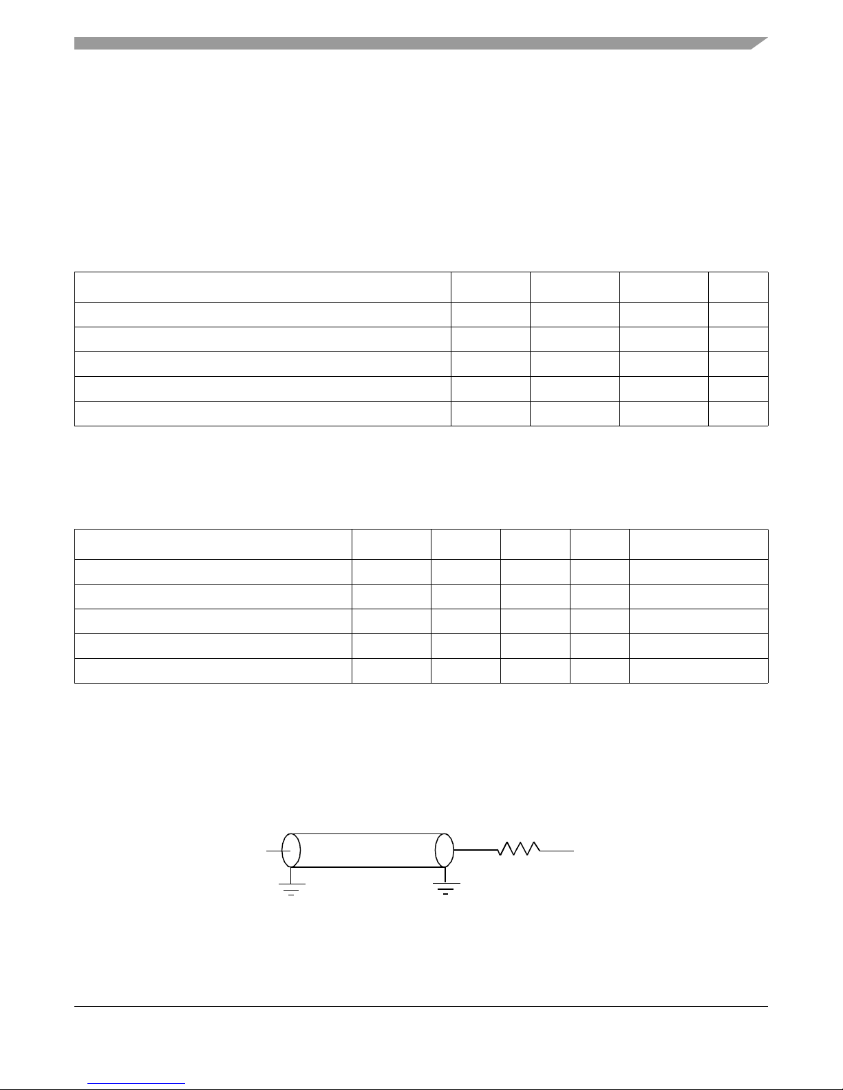
20 USB
Output
Z0 = 50 Ω
OVDD/2
R
L
= 50 Ω
This section provides the AC and DC electrical specifications for the USB interface of the
MPC8360E/58E.
20.1 USB DC Electrical Characteristics
Table 64 provides the DC electrical characteristics for the USB interface.
Table 64. USB DC Electrical Characteristics
Parameter Symbol Min Max Unit
USB
High-level input voltage V
Low-level input voltage V
High-level output voltage, I
Low-level output voltage, I
Input current I
= –100 μAV
OH
= 100 μAV
OL
IH
IL
OH
OL
IN
2OV
–0.3 0.8 V
OVDD – 0.4 — V
—0.2V
—±10μA
20.2 USB AC Electrical Specifications
Table 65 describes the general timing parameters of the USB interface of the device.
Table 65. USB General Timing Parameters
USCK
USCK
USTSPN
USRSPND
USRPND
1
Min Max Unit Notes
20.83 — ns Full speed 48 MHz
166.67 — ns Low speed 6 MHz
—5ns—
— 10 ns Full speed transitions
— 100 ns Low speed transitions
(first two letters of functional block)(state)(signal)
USRSPND
USTSPN
symbolizes USB timing (US) for the
symbolizes USB timing (US) for the USB
Parameter Symbol
USB clock cycle time t
USB clock cycle time t
Skew between TXP and TXN t
Skew among RXP, RXN, and RXD t
Skew among RXP, RXN, and RXD t
Notes:
1. The symbols used for timing specifications follow the pattern of t
and t
(first two letters of functional block)(state)(signal)
USB receive signals skew (RS) among RXP, RXN, and RXD (PND). Also, t
transmit signals skew (TS) between TXP and TXN (PN).
2.Skew measurements are done at OV
for transmit signals. For example, t
/2 of the rising or falling edge of the signals.
DD
+ 0.3 V
DD
for receive signals
Figure 52 provide the AC test load for the USB.
MPC8360E/MPC8358E PowerQUICC II Pro Processor Revision 2.x TBGA Silicon Hardware Specifications, Rev. 4
Freescale Semiconductor 67
Figure 52. USB AC Test Load
Page 68

Package and Pin Listings
21 Package and Pin Listings
This section details package parameters, pin assignments, and dimensions. The MPC8360E/58E is
available in a tape ball gr id array (TBGA), see Section 21.1, “Package Parameters for the TBGA Package,”
and Section 21.2, “Mechanical Dimensions of the TBGA Package,” for information on the package.
21.1 Package Parameters for the TBGA Package
The package parameters for rev. 2.0 silicon are as provided in the following list. The package type is
37.5 mm × 37.5 mm, 740 tape ball grid array (TBGA).
Package outline 37.5 mm × 37.5 mm
Interconnects 740
Pitch 1.00 mm
Module height (typical) 1.46 mm
Solder Balls 62 Sn/36 Pb/2 Ag (ZU package)
95.5 Sn/0.5 Cu/4Ag (VV package)
Ball diameter (typical) 0.64 mm
MPC8360E/MPC8358E PowerQUICC II Pro Processor Revision 2.x TBGA Silicon Hardware Specifications, Rev. 4
68 Freescale Semiconductor
Page 69
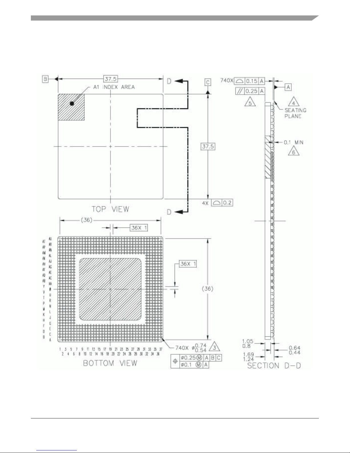
Package and Pin Listings
21.2 Mechanical Dimensions of the TBGA Package
Figure 53 depicts the mechanical dimensions and bottom surface nomenclature of the device, 740-TBGA
package.
Figure 53. Mechanical Dimensions and Bottom Surface Nomenclature of the TBGA Package
MPC8360E/MPC8358E PowerQUICC II Pro Processor Revision 2.x TBGA Silicon Hardware Specifications, Rev. 4
Freescale Semiconductor 69
Page 70
Package and Pin Listings
21.3 Pinout Listings
Refer to AN3097, “MPC8360/MPC8358E PowerQUICC Design Checklist,” for proper pin termination
and usage.
Table 66 shows the pin list of the MPC8360E TBGA package.
Table 66. MPC8360E TBGA Pinout Listing
Signal Package Pin Number Pin Type
Power
Supply
Primary DDR SDRAM Memory Controller Interface
MEMC1_MDQ[0:31] AJ34, AK33, AL33, AL35, AJ33, AK34, AK32,
I/O GV
AM36, AN37, AN35, AR34, AT34, AP37, AP36,
AR36, AT35, AP34, AR32, AP32, AM31, AN33,
AM34, AM33, AM30, AP31, AM27, AR30, AT32,
AN29, AP29, AN27, AR29
MEMC1_MDQ[32:63]/
MEMC2_MDQ[0:31]
AN8, AN7, AM8, AM6, AP9, AN9, AT7, AP7, AU6,
AP6, AR4, AR3, AT6, AT5, AR5, AT3, AP4, AM5,
I/O GV
AP3, AN3, AN5, AL5, AN4, AM2, AL2, AH5, AK3,
AJ2, AJ3, AH4, AK4, AH3
MEMC1_MECC[0:4]/
AP24, AN22, AM19, AN19, AM24 I/O GV
MSRCID[0:4]
MEMC1_MECC[5]/
AM23 I/O GV
MDVAL
MEMC1_MECC[6:7] AM22, AN18 I/O GV
MEMC1_MDM[0:3] AL36, AN34, AP33, AN28 O GV
MEMC1_MDM[4:7]/
AT9, AU4, AM3, AJ6 O GV
MEMC2_MDM[0:3]
MEMC1_MDM[8] AP27 O GV
MEMC1_MDQS[0:3] AK35, AP35, AN31, AM26 I/O GV
MEMC1_MDQS[4:7]/
AT8, AU3, AL4, AJ5 I/O GV
MEMC2_MDQS[0:3]
MEMC1_MDQS[8] AP26 I/O GV
MEMC1_MBA[0:1] AU29, AU30 O GV
MEMC1_MBA[2] AT30 O GV
MEMC1_MA[0:14] AU21, AP22, AP21, AT21, AU25, AU26, AT23,
OGV
AR26, AU24, AR23, AR28, AU23, AR22, AU20,
AR18
MEMC1_MODT[0:1] AG33, AJ36 O GV
MEMC1_MODT[2:3]/
AT1, AK2 O GV
MEMC2_MODT[0:1]
MEMC1_MWE
MEMC1_MRAS
MEMC1_MCAS
MEMC1_MCS
[0:1] AU27, AT27 O GV
AT 26 O G V
AT 29 O G V
AT 24 O G V
DD
DD
DD
DD
DD
DD
DD
DD
DD
DD
DD
DD
DD
DD
DD
DD
DD
DD
DD
DD
Notes
—
—
—
—
—
—
—
—
—
—
—
—
—
—
6
6
—
—
—
—
MPC8360E/MPC8358E PowerQUICC II Pro Processor Revision 2.x TBGA Silicon Hardware Specifications, Rev. 4
70 Freescale Semiconductor
Page 71
Table 66. MPC8360E TBGA Pinout Listing (continued)
Package and Pin Listings
Signal Package Pin Number Pin Type
MEMC1_MCS[2:3]/
MEMC2_MCS
[0:1]
AU8, AU7 O GV
Power
Supply
MEMC1_MCKE[0:1] AL32, AU33 O GV
MEMC1_MCK[0:1] AK37, AT37 O GV
MEMC1_MCK[2:3]/
AN1, AR2 O GV
MEMC2_MCK[0:1]
MEMC1_MCK[4:5]/
AN25, AK1 O GV
MEMC2_MCKE[0:1]
MEMC1_MCK
MEMC1_MCK
MEMC2_MCK
MEMC1_MCK
[0:1] AL37, AT36 O GV
[2:3]/
AP2, AT2 O GV
[0:1]
[4]/
AN24 O GV
MEMC2_MDM[8]
MEMC1_MCK
[5]/
AL1 O GV
MEMC2_MDQS[8]
MDIC[0:1] AH6, AP30 I/O GV
Secondary DDR SDRAM Memory Controller Interface
MEMC2_MECC[0:7] AN16, AP18, AM16, AM17, AN17, AP13, AP15,
I/O GV
AN13
MEMC2_MBA[0:2] AU12, AU15, AU13 O GV
MEMC2_MA[0:14] AT12, AP11, AT13, AT14, AR13, AR15, AR16,
OGV
AT16, AT18, AT17, AP10, AR20, AR17, AR14,
AR11
MEMC2_MWE
MEMC2_MRAS
MEMC2_MCAS
AU10 O GV
AT 11 O G V
AU11 O GV
PCI
DD
DD
DD
DD
DD
DD
DD
DD
DD
DD
DD
DD
DD
DD
DD
DD
Notes
—
3
—
—
—
—
—
—
—
10
—
—
—
—
—
—
PCI_INTA
PCI_RESET_OUT
/IRQ_OUT/CE_PF[5] A20 I/O LVDD22
/CE_PF[6] E19 I/O LVDD2—
PCI_AD[31:30]/CE_PG[31:30] D20, D21 I/O LV
PCI_AD[29:25]/CE_PG[29:25] A24, B23, C23, E23, A26 I/O OV
PCI_AD[24]/CE_PG[24] B21 I/O LV
PCI_AD[23:0]/CE_PG[23:0] C24, C25, D25, B25, E24, F24, A27, A28, F27, A30,
PCI_C/BE
[3:0]/CE_PF[10:7] E22, B26, E28, F28 I/O OV
PCI_PAR/CE_PF[11] D28 I/O OV
PCI_FRAME
/CE_PF[12] D26 I/O OV
PCI_TRDY/CE_PF[13] C27 I/O OV
MPC8360E/MPC8358E PowerQUICC II Pro Processor Revision 2.x TBGA Silicon Hardware Specifications, Rev. 4
Freescale Semiconductor 71
C30, D30, E29, B31, C31, D31, D32, A32, C33,
B33, F30, E31, A34, D33
I/O OV
2—
DD
DD
2—
DD
DD
DD
DD
DD
DD
—
—
—
—
5
5
Page 72
Package and Pin Listings
Table 66. MPC8360E TBGA Pinout Listing (continued)
Signal Package Pin Number Pin Type
Power
Supply
PCI_IRDY/CE_PF[14] C28 I/O OV
PCI_STOP
PCI_DEVSEL
/CE_PF[15] B28 I/O OV
/CE_PF[16] E26 I/O OV
PCI_IDSEL/CE_PF[17] F22 I/O OV
PCI_SERR
PCI_PERR
/CE_PF[18] B29 I/O OV
/CE_PF[19] A29 I/O OV
PCI_REQ[0]/CE_PF[20] F19 I/O LV
PCI_REQ
[1]/CPCI_HS_ES/
A21 I/O LVDD2—
CE_PF[21]
PCI_REQ
PCI_GNT
PCI_GNT
[2]/CE_PF[22] C21 I/O LVDD2—
[0]/CE_PF[23] E20 I/O LVDD2—
[1]/CPCI1_HS_LED/
B20 I/O LVDD2—
CE_PF[24]
PCI_GNT
[2]/CPCI1_HS_ENUM/
C20 I/O LVDD2—
CE_PF[25]
PCI_MODE
D36 I OV
M66EN/CE_PF[4] B37 I/O OV
Local Bus Controller Interface
Notes
DD
DD
DD
DD
DD
DD
2—
DD
DD
DD
5
5
5
—
5
5
—
—
LAD[0:31] N32, N33, N35, N36, P37, P32, P34, R36, R35,
I/O OV
R34, R33, T37, T35, T34, T33, U37, T32, U36, U34,
V36, V35, W37, W35, V33, V32, W34, Y36, W32,
AA37, Y33, AA35, AA34
LDP[0]/CKSTOP_OUT
LDP[1]/CKSTOP_IN
LDP[2]/LCS
LDP[3]/LCS
[6] AB35 I/O OV
[7] AA33 I/O OV
AB37 I/O OV
AB36 I/O OV
LA[27:31] AC37, AA32, AC36, AC34, AD36 O OV
LCS
[0:5] AD33, AG37, AF34, AE33, AD32, AH37 O OV
[0:3]/LSDDQM[0:3]/LBS[0:3] AG35, AG34, AH36, AE32 O OV
LWE
LBCTL AD35 O OV
LALE M37 O OV
LGPL0/LSDA10/cfg_reset_source0 AB32 I/O OV
LGPL1/LSDWE
LGPL2/LSDRAS
LGPL3/LSDCAS/
LGPL4/LGTA
/cfg_reset_source1 AE37 I/O OV
/LOE AC33 O OV
cfg_reset_source2 AD34 I/O OV
/LUPWAIT/LPBSE AE35 I/O OV
LGPL5/cfg_clkin_div AF36 I/O OV
LCKE G36 O OV
DD
DD
DD
DD
DD
DD
DD
DD
DD
DD
DD
DD
DD
DD
DD
DD
DD
—
—
—
—
—
—
—
—
—
—
—
—
—
—
—
—
—
MPC8360E/MPC8358E PowerQUICC II Pro Processor Revision 2.x TBGA Silicon Hardware Specifications, Rev. 4
72 Freescale Semiconductor
Page 73
Table 66. MPC8360E TBGA Pinout Listing (continued)
Package and Pin Listings
Signal Package Pin Number Pin Type
Power
Supply
LCLK[0] J33 O OV
LCLK[1]/LCS[6] J34 O OV
LCLK[2]/LCS[7] G37 O OV
LSYNC_OUT F34 O OV
LSYNC_IN G35 I OV
Programmable Interrupt Controller
MCP_OUT
0/MCP_IN C37 I OV
IRQ
IRQ[1]/M1SRCID[4]/M2SRCID[4]/
E34 O OV
F35 I/O OV
LSRCID[4]
IRQ
[2]/M1DVAL/M2DVAL/LDVAL F36 I/O OV
IRQ
[3]/CORE_SRESET H34 I/O OV
IRQ
[4:5] G33, G32 I/O OV
[6]/LCS[6]/CKSTOP_OUT E35 I/O OV
IRQ
IRQ
[7]/LCS[7]/CKSTOP_IN H36 I/O OV
DUART
UART1_SOUT/M1SRCID[0]/
E32 O OV
M2SRCID[0]/LSRCID[0]
UART1_SIN/M1SRCID[1]/
B34 I/O OV
M2SRCID[1]/LSRCID[1]
UART1_CTS
/M1SRCID[2]/
C34 I/O OV
M2SRCID[2]/LSRCID[2]
UART1_RTS
/M1SRCID[3]/
A35 O OV
M2SRCID[3]/LSRCID[3]
2
C Interface
I
DD
DD
DD
DD
DD
DD
DD
DD
DD
DD
DD
DD
DD
DD
DD
DD
DD
Notes
—
—
—
—
—
2
—
—
—
—
—
—
—
—
—
—
—
IIC1_SDA D34 I/O OV
IIC1_SCL B35 I/O OV
IIC2_SDA E33 I/O OV
IIC2_SCL C35 I/O OV
CE_PA[0] F8 I/O LV
CE_PA[1:2] AH1, AG5 I/O OV
CE_PA[3:7] F6, D4, C3, E5, A3 I/O LV
CE_PA[8] AG3 I/O OV
CE_PA[9:12] F7, B3, E6, B4 I/O LV
CE_PA[13:14] AG1, AF6 I/O OV
CE_PA[15] B2 I/O LV
MPC8360E/MPC8358E PowerQUICC II Pro Processor Revision 2.x TBGA Silicon Hardware Specifications, Rev. 4
Freescale Semiconductor 73
QUICC Engine Block
DD
DD
DD
DD
DD0
DD
0—
DD
DD
0—
DD
DD
0—
DD
2
2
2
2
—
—
—
—
Page 74
Package and Pin Listings
Table 66. MPC8360E TBGA Pinout Listing (continued)
Signal Package Pin Number Pin Type
Power
Supply
CE_PA[16] AF4 I/O OV
CE_PA[17:21] B16, A16, E17, A17, B17 I/O LV
CE_PA[22] AF3 I/O OV
CE_PA[23:26] C18, D18, E18, A18 I/O LV
CE_PA[27:28] AF2, AE6 I/O OV
CE_PA[29] B19 I/O LV
CE_PA[30] AE5 I/O OV
CE_PA[31] F16 I/O LV
CE_PB[0:27] AE2, AE1, AD5, AD3, AD2, AC6, AC5, AC4, AC2,
I/O OV
AC1, AB5, AB4, AB3, AB1, AA6, AA4, AA2, Y6, Y4,
Y3, Y2, Y1, W6, W5, W2, V5, V3, V2
CE_PC[0:1] V1, U6 I/O OV
CE_PC[2:3] C16, A15 I/O LV
CE_PC[4:6] U4, U3, T6 I/O OV
CE_PC[7] C19 I/O LV
CE_PC[8:9] A4, C5 I/O LV
CE_PC[10:30] T5, T4, T2, T1, R5, R3, R1, C11, D12, F13, B10,
I/O OV
C10, E12, A9, B8, D10, A14, E15, B14, D15, AH2
CE_PD[0:27] E11, D9, C8, F11, A7, E9, C7, A6, F10, B6, D7, E8,
I/O OV
B5, A5, C2, E4, F5, B1, D2, G5, D1, E2, H6, F3, E1,
F2, G3, H4
CE_PE[0:31] K3, J2, F1, G2, J5, H3, G1, H2, K6, J3, K5, K4, L6,
I/O OV
P6, P4, P3, P1, N4, N5, N2, N1, M2, M3, M5, M6,
L1, L2, L4, E14, C13, C14, B13
CE_PF[0:3] F14, D13, A12, A11 I/O OV
Clocks
Notes
DD
1—
DD
DD
1—
DD
DD
1—
DD
DD
1—
DD
DD
DD
1—
DD
DD
2—
DD
0—
DD
DD
DD
DD
DD
—
—
—
—
—
—
—
—
—
—
—
PCI_CLK_OUT[0]/CE_PF[26] B22 I/O LV
PCI_CLK_OUT[1:2]/CE_PF[27:28] D22, A23 I/O OV
CLKIN E37 I OV
PCI_CLOCK/PCI_SYNC_IN M36 I OV
PCI_SYNC_OUT/CE_PF[29] D37 I/O OV
TCK K33 I OV
TDI K34 I OV
TDO H37 O OV
TMS J36 I OV
TRST L32 I OV
MPC8360E/MPC8358E PowerQUICC II Pro Processor Revision 2.x TBGA Silicon Hardware Specifications, Rev. 4
74 Freescale Semiconductor
JTAG
Test
2—
DD
DD
DD
DD
DD
DD
DD
DD
DD
DD
—
—
—
3
—
4
3
4
4
Page 75
Table 66. MPC8360E TBGA Pinout Listing (continued)
Package and Pin Listings
Signal Package Pin Number Pin Type
Power
Supply
TEST L35 I OV
TEST_SEL AU34 I GV
PMC
QUIESCE
B36 O OV
System Control
PORESET
HRESET
L37 I OV
L36 I/O OV
SRESET M33 I/O OV
Thermal Management
THERM0 AP19 I GV
THERM1 AT31 I GV
Power and Ground Signals
AV
1 K35 Power for
DD
AV
LBIU DLL
(1.2 V)
2 K36 Power for
AV
DD
AV
CE PLL
(1.2 V)
5 AM29 Power for
AV
DD
AV
e300 PLL
(1.2 V)
6 K37 Power for
AV
DD
AV
system
PLL (1.2 V)
GND A2, A8, A13, A19, A22, A25, A31, A33, A36, B7,
———
B12, B24, B27, B30, C4, C6, C9, C15, C26, C32,
D3, D8, D11, D14, D17, D19, D23, D27, E7, E13,
E25, E30, E36, F4, F37, G34, H1, H5, H32, H33, J4,
J32, J37, K1, L3, L5, L33, L34, M1, M34, M35, N37,
P2, P5, P35, P36, R4, T3, U1, U5, U35, V37, W1,
W4, W33, W36, Y34, AA3, AA5, AC3, AC32, AC35,
AD1, AD37, AE4, AE34, AE36, AF33, AG4, AG6,
AG32, AH35, AJ1, AJ4, AJ32, AJ35, AJ37, AK36,
AL3, AL34, AM4, AN6, AN23, AN30, AP8, AP12,
AP14, AP16, AP17, AP20, AP25, AR6, AR8, AR9,
AR19, AR24, AR31, AR35, AR37, AT4, AT10, AT19,
AT20, AT25, AU14, AU22, AU28, AU35
GV
DD
AD4, AE3, AF1, AF5, AF35, AF37, AG2, AG36,
AH33, AH34, AK5, AM1, AM35, AM37, AN2, AN10,
AN11, AN12, AN14, AN32, AN36, AP5, AP23,
AP28, AR1, AR7, AR10, AR12, AR21, AR25, AR27,
AR33, AT15, AT22, AT28, AT33, AU2, AU5, AU16,
AU31, AU36
Power for
DDR
DRAM I/O
voltage
(2.5 or
1.8 V)
GV
Notes
DD
DD
DD
DD
DD
DD
DD
DD
1—
DD
2—
DD
5—
DD
6—
DD
DD
7
7
—
—
1
2
—
—
—
MPC8360E/MPC8358E PowerQUICC II Pro Processor Revision 2.x TBGA Silicon Hardware Specifications, Rev. 4
Freescale Semiconductor 75
Page 76
Package and Pin Listings
Table 66. MPC8360E TBGA Pinout Listing (continued)
Signal Package Pin Number Pin Type
LVDD0 D5, D6 Power for
Power
Supply
LV
0—
DD
Notes
UCC1
Ethernet
interface
(2.5 V,
3.3 V)
LV
1 C17, D16 Power for
DD
LV
19
DD
UCC2
Ethernet
interface
option 1
(2.5 V,
3.3 V)
LV
2 B18, E21 Power for
DD
LV
29
DD
UCC2
Ethernet
interface
option 2
(2.5 V,
3.3 V)
V
DD
C36, D29, D35, E16, F9, F12, F15, F17, F18, F20,
F21, F23, F25, F26, F29, F31, F32, F33, G6, J6,
K32, M32, N6, P33, R6, R32, U32, V6, Y5, Y32,
Power for
core
(1.2 V)
V
DD
—
AB6, AB33, AD6, AF32, AK6, AL6, AM7, AM9,
AM10, AM11, AM12, AM13, AM14, AM15, AM18,
AM21, AM25, AM28, AM32, AN15, AN21, AN26,
AU9, AU17
OV
DD
A10, B9, B15, B32, C1, C12, C22, C29, D24, E3,
E10, E27, G4, H35, J1, J35, K2, M4, N3, N34, R2,
R37, T36, U2, U33, V4, V34, W3, Y35, Y37, AA1,
AA36, AB2, AB34
PCI,
10/100
Ethernet,
and other
OV
DD
—
standard
(3.3 V)
MVREF1 AN20 I DDR
—
reference
voltage
MVREF2 AU32 I DDR
—
reference
voltage
SPARE1 B11 I/O OV
SPARE3 AH32 — GV
SPARE4 AU18 — GV
SPARE5 AP1 — GV
MPC8360E/MPC8358E PowerQUICC II Pro Processor Revision 2.x TBGA Silicon Hardware Specifications, Rev. 4
76 Freescale Semiconductor
DD
DD
DD
DD
8
8
7
8
Page 77
Table 66. MPC8360E TBGA Pinout Listing (continued)
Package and Pin Listings
Signal Package Pin Number Pin Type
Power
Supply
Notes
No Connect
NC AM20, AU19 — — —
Notes:
1. This pin is an open drain signal. A weak pull-up resistor (1 kΩ) should be placed on this pin to OV
DD
2. This pin is an open drain signal. A weak pull-up resistor (2–10 kΩ) should be placed on this pin to OVDD.
3. This output is actively driven during reset rather than being three-stated during reset.
4. These JTAG pins have weak internal pull-up P-FETs that are always enabled.
5. This pin should have a weak pull up if the chip is in PCI host mode. Follow PCI specifications recommendation.
6. These are On Die Termination pins, used to control DDR2 memories internal termination resistance
7. This pin must always be tied to GND.
8. This pin must always be left not connected.
9. Refers to
MPC8360E PowerQUICC II Pro Integrated Communications Processor Family Reference Manual
section on
“RGMII Pins,” for information about the two UCC2 Ethernet interface options.
10. It is recommended that MDIC0 be tied to GND using an 18.2 Ω resistor and MDIC1 be tied to DDR power using an 18.2 Ω
resistor for DDR2.
Table 67 shows the pin list of the MPC8358E TBGA package.
Table 67. MPC8358E TBGA Pinout Listing
Signal Package Pin Number Pin Type
Power
Supply
Notes
DDR SDRAM Memory Controller Interface
MEMC1_MDQ[0:63] AJ34, AK33, AL33, AL35, AJ33, AK34, AK32,
I/O GV
AM36, AN37, AN35, AR34, AT34, AP37, AP36,
AR36, AT35, AP34, AR32, AP32, AM31, AN33,
AM34, AM33, AM30, AP31, AM27, AR30, AT32,
AN29, AP29, AN27, AR29, AN8, AN7, AM8, AM6,
AP9, AN9, AT7, AP7, AU6, AP6, AR4, AR3, AT6,
AT5, AR5, AT3, AP4, AM5, AP3, AN3, AN5, AL5,
AN4, AM2, AL2, AH5, AK3, AJ2, AJ3, AH4, AK4,
AH3
MEMC_MECC[0:4]/MSRCID[0:4] AP24, AN22, AM19, AN19, AM24 I/O GV
MEMC_MECC[5]/MDVAL AM23 I/O GV
MEMC_MECC[6:7] AM22, AN18 I/O GV
MEMC_MDM[0:8] AL36, AN34, AP33, AN28,AT9, AU4, AM3,
OGV
AJ6,AP27
MEMC_MDQS[0:8] AK35, AP35, AN31, AM26,AT8, AU3, AL4, AJ5,
I/O GV
AP26
MEMC_MBA[0:1] AU29, AU30 O GV
MEMC_MBA[2] AT30 O GV
MEMC_MA[0:14] AU21, AP22, AP21, AT21, AU25, AU26, AT23,
OGV
AR26, AU24, AR23, AR28, AU23, AR22, AU20,
AR18
DD
DD
DD
DD
DD
DD
DD
DD
DD
—
—
—
—
—
—
—
—
MPC8360E/MPC8358E PowerQUICC II Pro Processor Revision 2.x TBGA Silicon Hardware Specifications, Rev. 4
Freescale Semiconductor 77
Page 78
Package and Pin Listings
Table 67. MPC8358E TBGA Pinout Listing (continued)
Signal Package Pin Number Pin Type
Power
Supply
MEMC_MODT[0:3] AG33, AJ36, AT1, AK2 O GV
MEMC_MWE
MEMC_MRAS
MEMC_MCAS
MEMC_MCS
[0:3] AU27, AT27, AU8, AU7 O GV
AT 26 O G V
AT 29 O G V
AT 24 O G V
MEMC_MCKE[0:1] AL32, AU33 O GV
MEMC_MCK[0:5] AK37, AT37, AN1, AR2, AN25, AK1 O GV
MEMC_MCK
[0:5] AL37, AT36, AP2, AT2, AN24, AL1 O GV
MDIC[0:1] AH6, AP30 I/O GV
PCI
PCI_INTA
PCI_RESET_OUT
/IRQ_OUT/CE_PF[5] A20 I/O LVDD22
/CE_PF[6] E19 I/O LVDD2—
PCI_AD[31:30]/CE_PG[31:30] D20, D21 I/O LV
PCI_AD[29:25]/CE_PG[29:25] A24, B23, C23, E23, A26 I/O OV
PCI_AD[24]/CE_PG[24] B21 I/O LV
PCI_AD[23:0]/CE_PG[23:0] C24, C25, D25, B25, E24, F24, A27, A28, F27, A30,
I/O OV
C30, D30, E29, B31, C31, D31, D32, A32, C33,
B33, F30, E31, A34, D33
Notes
DD
DD
DD
DD
DD
DD
DD
DD
DD
2—
DD
DD
2—
DD
DD
6
—
—
—
—
3
—
—
11
—
—
PCI_C/BE
[3:0]/CE_PF[10:7] E22, B26, E28, F28 I/O OV
PCI_PAR/CE_PF[11] D28 I/O OV
PCI_FRAME
PCI_TRDY
PCI_IRDY
PCI_STOP
PCI_DEVSEL
/CE_PF[12] D26 I/O OV
/CE_PF[13] C27 I/O OV
/CE_PF[14] C28 I/O OV
/CE_PF[15] B28 I/O OV
/CE_PF[16] E26 I/O OV
PCI_IDSEL/CE_PF[17] F22 I/O OV
PCI_SERR
PCI_PERR
PCI_REQ
PCI_REQ
/CE_PF[18] B29 I/O OV
/CE_PF[19] A29 I/O OV
[0]/CE_PF[20] F19 I/O LVDD2—
[1]/CPCI_HS_ES/
A21 I/O LVDD2—
CE_PF[21]
PCI_REQ
PCI_GNT
PCI_GNT
[2]/CE_PF[22] C21 I/O LVDD2—
[0]/CE_PF[23] E20 I/O LVDD2—
[1]/CPCI1_HS_LED/
B20 I/O LVDD2—
CE_PF[24]
DD
DD
DD
DD
DD
DD
DD
DD
DD
DD
—
—
5
5
5
5
5
—
5
5
MPC8360E/MPC8358E PowerQUICC II Pro Processor Revision 2.x TBGA Silicon Hardware Specifications, Rev. 4
78 Freescale Semiconductor
Page 79
Table 67. MPC8358E TBGA Pinout Listing (continued)
Package and Pin Listings
Signal Package Pin Number Pin Type
PCI_GNT[2]/CPCI1_HS_ENUM/
C20 I/O LVDD2—
Power
Supply
CE_PF[25]
PCI_MODE
D36 I OV
M66EN/CE_PF[4] B37 I/O OV
Local Bus Controller Interface
LAD[0:31] N32, N33, N35, N36, P37, P32, P34, R36, R35,
I/O OV
R34, R33, T37, T35, T34, T33, U37, T32, U36, U34,
V36, V35, W37, W35, V33, V32, W34, Y36, W32,
AA37, Y33, AA35, AA34
LDP[0]/CKSTOP_OUT
LDP[1]/CKSTOP_IN
LDP[2]/LCS
LDP[3]/LCS
[6] AB35 I/O OV
[7] AA33 I/O OV
AB37 I/O OV
AB36 I/O OV
LA[27:31] AC37, AA32, AC36, AC34, AD36 O OV
LCS
[0:5] AD33, AG37, AF34, AE33, AD32, AH37 O OV
[0:3]/LSDDQM[0:3]/LBS[0:3] AG35, AG34, AH36, AE32 O OV
LWE
LBCTL AD35 O OV
LALE M37 O OV
LGPL0/LSDA10/cfg_reset_source0 AB32 I/O OV
LGPL1/LSDWE
LGPL2/LSDRAS
LGPL3/LSDCAS
LGPL4/LGTA
/cfg_reset_source1 AE37 I/O OV
/LOE AC33 O OV
/cfg_reset_source2 AD34 I/O OV
/LUPWAIT/LPBSE AE35 I/O OV
LGPL5/cfg_clkin_div AF36 I/O OV
LCKE G36 O OV
LCLK[0] J33 O OV
LCLK[1]/LCS[6] J34 O OV
LCLK[2]/LCS[7] G37 O OV
LSYNC_OUT F34 O OV
LSYNC_IN G35 I OV
Programmable Interrupt Controller
DD
DD
DD
DD
DD
DD
DD
DD
DD
DD
DD
DD
DD
DD
DD
DD
DD
DD
DD
DD
DD
DD
DD
DD
Notes
—
—
—
—
—
—
—
—
—
—
—
—
—
—
—
—
—
—
—
—
—
—
—
—
MCP_OUT
IRQ
0/MCP_IN C37 I OV
IRQ
[1]/M1SRCID[4]/M2SRCID[4]/
LSRCID[4]
MPC8360E/MPC8358E PowerQUICC II Pro Processor Revision 2.x TBGA Silicon Hardware Specifications, Rev. 4
Freescale Semiconductor 79
E34 O OV
F35 I/O OV
DD
DD
DD
2
—
—
Page 80
Package and Pin Listings
Table 67. MPC8358E TBGA Pinout Listing (continued)
Signal Package Pin Number Pin Type
Power
Supply
IRQ[2]/M1DVAL/M2DVAL/LDVAL F36 I/O OV
IRQ
[3]/CORE_SRESET H34 I/O OV
IRQ
[4:5] G33, G32 I/O OV
IRQ
[6]/LCS[6]/CKSTOP_OUT E35 I/O OV
IRQ
[7]/LCS[7]/CKSTOP_IN H36 I/O OV
DUART
UART1_SOUT/M1SRCID[0]/
E32 O OV
M2SRCID[0]/LSRCID[0]
UART1_SIN/M1SRCID[1]/
B34 I/O OV
M2SRCID[1]/LSRCID[1]
UART1_CTS
/M1SRCID[2]/
C34 I/O OV
M2SRCID[2]/LSRCID[2]
UART1_RTS
/M1SRCID[3]/
A35 O OV
M2SRCID[3]/LSRCID[3]
2
C Interface
I
IIC1_SDA D34 I/O OV
IIC1_SCL B35 I/O OV
IIC2_SDA E33 I/O OV
IIC2_SCL C35 I/O OV
QUICC Engine
DD
DD
DD
DD
DD
DD
DD
DD
DD
DD
DD
DD
DD
Notes
—
—
—
—
—
—
—
—
—
2
2
2
2
CE_PA[0] F8 I/O LV
CE_PA[1:2] AH1, AG5 I/O OV
CE_PA[3:7] F6, D4, C3, E5, A3 I/O LV
CE_PA[8] AG3 I/O OV
CE_PA[9:12] F7, B3, E6, B4 I/O LV
CE_PA[13:14] AG1, AF6 I/O OV
CE_PA[15] B2 I/O LV
CE_PA[16] AF4 I/O OV
CE_PA[17:21] B16, A16, E17, A17, B17 I/O LV
CE_PA[22] AF3 I/O OV
CE_PA[23:26] C18, D18, E18, A18 I/O LV
CE_PA[27:28] AF2, AE6 I/O OV
CE_PA[29] B19 I/O LV
CE_PA[30] AE5 I/O OV
CE_PA[31] F16 I/O LV
DD0
DD
0—
DD
DD
0—
DD
DD
0—
DD
DD
1—
DD
DD
1—
DD
DD
1—
DD
DD
1—
DD
MPC8360E/MPC8358E PowerQUICC II Pro Processor Revision 2.x TBGA Silicon Hardware Specifications, Rev. 4
—
—
—
—
—
—
—
—
80 Freescale Semiconductor
Page 81
Table 67. MPC8358E TBGA Pinout Listing (continued)
Package and Pin Listings
Signal Package Pin Number Pin Type
CE_PB[0:27] AE2, AE1, AD5, AD3, AD2, AC6, AC5, AC4, AC2,
I/O OV
Power
Supply
DD
Notes
—
AC1, AB5, AB4, AB3, AB1, AA6, AA4, AA2, Y6, Y4,
Y3, Y2, Y1, W6, W5, W2, V5, V3, V2
CE_PC[0:1] V1, U6 I/O OV
DD
CE_PC[2:3] C16, A15 I/O LVDD1—
CE_PC[4:6] U4, U3, T6 I/O OV
CE_PC[7] C19 I/O LV
CE_PC[8:9] A4, C5 I/O LV
CE_PC[10:30] T5, T4, T2, T1, R5, R3, R1, C11, D12, F13, B10,
I/O OV
DD
2—
DD
0—
DD
DD
—
—
C10, E12, A9, B8, D10, A14, E15, B14, D15, AH2
CE_PD[0:27] E11, D9, C8, F11, A7, E9, C7, A6, F10, B6, D7, E8,
I/O OV
DD
—
B5, A5, C2, E4, F5, B1, D2, G5, D1, E2, H6, F3, E1,
F2, G3, H4
CE_PE[0:31] K3, J2, F1, G2, J5, H3, G1, H2, K6, J3, K5, K4, L6,
I/O OV
DD
—
P6, P4, P3, P1, N4, N5, N2, N1, M2, M3, M5, M6,
L1, L2, L4, E14, C13, C14, B13
CE_PF[0:3] F14, D13, A12, A11 I/O OV
DD
—
Clocks
PCI_CLK_OUT[0]/CE_PF[26] B22 I/O LV
PCI_CLK_OUT[1:2]/CE_PF[27:28] D22, A23 I/O OV
CLKIN E37 I OV
PCI_CLOCK/PCI_SYNC_IN M36 I OV
PCI_SYNC_OUT/CE_PF[29] D37 I/O OV
JTAG
TCK K33 I OV
TDI K34 I OV
TDO H37 O OV
TMS J36 I OV
TRST
L32 I OV
Test
TEST L35 I OV
TEST_SEL
AU34 I GV
PMC
QUIESCE
B36 O OV
System Control
2—
DD
DD
DD
DD
DD
DD
DD
DD
DD
DD
DD
DD
DD
—
—
—
3
—
4
3
4
4
7
10
—
MPC8360E/MPC8358E PowerQUICC II Pro Processor Revision 2.x TBGA Silicon Hardware Specifications, Rev. 4
Freescale Semiconductor 81
Page 82
Package and Pin Listings
Table 67. MPC8358E TBGA Pinout Listing (continued)
Signal Package Pin Number Pin Type
Power
Supply
PORESET L37 I OV
HRESET
SRESET
L36 I/O OV
M33 I/O OV
Thermal Management
THERM0 AP19 I GV
THERM1 AT31 I GV
Power and Ground Signals
AV
1 K35 Power for
DD
AV
LBIU DLL
(1.2 V)
AV
2 K36 Power for
DD
AV
CE PLL
(1.2 V)
5 AM29 Power for
AV
DD
AV
e300 PLL
(1.2 V)
AV
6 K37 Power for
DD
AV
system
PLL (1.2 V)
GND A2, A8, A13, A19, A22, A25, A31, A33, A36, B7,
———
B12, B24, B27, B30, C4, C6, C9, C15, C26, C32,
D3, D8, D11, D14, D17, D19, D23, D27, E7, E13,
E25, E30, E36, F4, F37, G34, H1, H5, H32, H33, J4,
J32, J37, K1, L3, L5, L33, L34, M1, M34, M35, N37,
P2, P5, P35, P36, R4, T3, U1, U5, U35, V37, W1,
W4, W33, W36, Y34, AA3, AA5, AC3, AC32, AC35,
AD1, AD37, AE4, AE34, AE36, AF33, AG4, AG6,
AG32, AH35, AJ1, AJ4, AJ32, AJ35, AJ37, AK36,
AL3, AL34, AM4, AN6, AN23, AN30, AP8, AP12,
AP14, AP16, AP17, AP20, AP25, AR6, AR8, AR9,
AR19, AR24, AR31, AR35, AR37, AT4, AT10, AT19,
AT20, AT25, AU14, AU22, AU28, AU35
Notes
DD
DD
DD
DD
DD
DD
DD
DD
DD
—
1
2
—
—
1—
2—
5—
6—
GV
DD
LV
0 D5, D6 Power for
DD
MPC8360E/MPC8358E PowerQUICC II Pro Processor Revision 2.x TBGA Silicon Hardware Specifications, Rev. 4
82 Freescale Semiconductor
AD4, AE3, AF1, AF5, AF35, AF37, AG2, AG36,
AH33, AH34, AK5, AM1, AM35, AM37, AN2, AN10,
AN11, AN12, AN14, AN32, AN36, AP5, AP23,
AP28, AR1, AR7, AR10, AR12, AR21, AR25, AR27,
AR33, AT15, AT22, AT28, AT33, AU2, AU5, AU16,
AU31, AU36
Power for
DDR
DRAM I/O
voltage
(2.5 or
1.8 V)
UCC1
Ethernet
interface
(2.5 V,
3.3 V)
GV
DD
LV
0—
DD
—
Page 83
Table 67. MPC8358E TBGA Pinout Listing (continued)
Package and Pin Listings
Signal Package Pin Number Pin Type
LVDD1 C17, D16 Power for
UCC2
Ethernet
interface
option 1
(2.5 V,
3.3 V)
LV
2 B18, E21 Power for
DD
UCC2
Ethernet
interface
option 2
(2.5 V,
3.3 V)
V
DD
C36, D29, D35, E16, F9, F12, F15, F17, F18, F20,
F21, F23, F25, F26, F29, F31, F32, F33, G6, J6,
K32, M32, N6, P33, R6, R32, U32, V6, Y5, Y32,
Power for
core
(1.2 V)
AB6, AB33, AD6, AF32, AK6, AL6, AM7, AM9,
AM10, AM11, AM12, AM13, AM14, AM15, AM18,
AM21, AM25, AM28, AM32, AN15, AN21, AN26,
AU9, AU17
OV
DD
A10, B9, B15, B32, C1, C12, C22, C29, D24, E3,
E10, E27, G4, H35, J1, J35, K2, M4, N3, N34, R2,
R37, T36, U2, U33, V4, V34, W3, Y35, Y37, AA1,
AA36, AB2, AB34
PCI,
10/100
Ethernet,
and other
standard
(3.3 V)
Power
Supply
LV
19
DD
LV
29
DD
V
DD
OV
DD
Notes
—
—
MVREF1 AN20 I DDR
—
reference
voltage
MVREF2 AU32 I DDR
—
reference
voltage
SPARE1 B11 I/O OV
SPARE3 AH32 — GV
SPARE4 AU18 — GV
SPARE5 AP1 — GV
DD
DD
DD
DD
8
8
7
8
MPC8360E/MPC8358E PowerQUICC II Pro Processor Revision 2.x TBGA Silicon Hardware Specifications, Rev. 4
Freescale Semiconductor 83
Page 84
Package and Pin Listings
Table 67. MPC8358E TBGA Pinout Listing (continued)
Signal Package Pin Number Pin Type
Power
Supply
Notes
No Connect
NC AM16, AM17, AM20, AN13, AN16, AN17, AP10,
———
AP11, AP13, AP15, AP18, AR11, AR13, AR14,
AR15, AR16, AR17, AR20, AT11, AT12, AT13,
AT14, AT16, AT17, AT18, AU10, AU11, AU12,
AU13, AU15, AU19
Notes:
1. This pin is an open drain signal. A weak pull-up resistor (1 kΩ) should be placed on this pin to OV
DD.
2. This pin is an open drain signal. A weak pull-up resistor (2–10 kΩ) should be placed on this pin to OVDD.
3. This output is actively driven during reset rather than being three-stated during reset.
4. These JTAG pins have weak internal pull-up P-FETs that are always enabled.
5. This pin should have a weak pull up if the chip is in PCI host mode. Follow PCI specifications recommendation.
6. These are On Die Termination pins, used to control DDR2 memories internal termination resistance.
7. This pin must always be tied to GND.
8. This pin must always be left not connected.
9. Refers to
MPC8360E PowerQUICC II Pro Integrated Communications Processor Family Reference Manual
section on
“RGMII Pins,” for information about the two UCC2 Ethernet interface options.
10.This pin must always be tied to GV
DD
.
11. It is recommended that MDIC0 be tied to GND using an 18.2 Ω resistor and MDIC1 be tied to DDR power using an 18.2 Ω
resistor for DDR2.
MPC8360E/MPC8358E PowerQUICC II Pro Processor Revision 2.x TBGA Silicon Hardware Specifications, Rev. 4
84 Freescale Semiconductor
Page 85
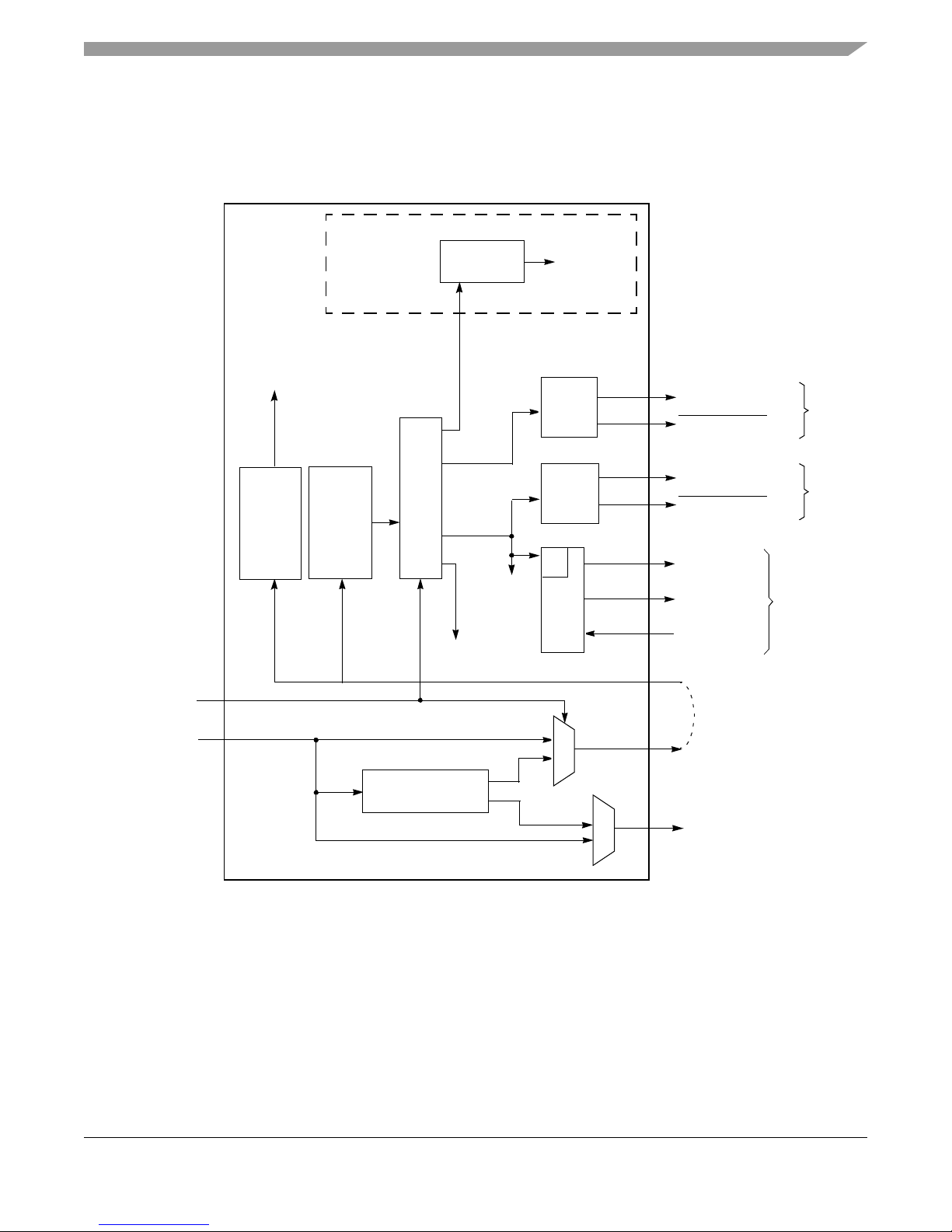
22 Clocking
Core PLL
System
DDRC2
LBIU
LSYNC_IN
LSYNC_OUT
LCLK[0:2]
MEMC2_MCK[0:1]
MEMC2_MCK
[0:1]
core_clk
e300 Core
csb_clk to Rest
CLKIN
csb_clk
MPC8360E
DDRC2
Memory
Local Bus
PCI_CLK_OUT[0:2]
PCI_SYNC_OUT
PCI_CLK/
Clock
Unit
of the Device
lb_clk
CFG_CLKIN_DIV
PCI Clock
PCI_SYNC_IN
Device
Memory
Device
/n
To Local
Bus/DDRC2
Controller
DLL
/2
Divider
MEMC1_MCK[0:5]
MEMC1_MCK
[0:5]
DDRC1
/2
ddr1_clk
DDRC1
Memory
Device
PLL
QUICC
PLL
ce_clk to QUICC Engine Block
Engine
Figure 54 shows the internal distribution of clocks within the MPC8360E.
Clocking
Figure 54. MPC8360E Clock Subsystem
MPC8360E/MPC8358E PowerQUICC II Pro Processor Revision 2.x TBGA Silicon Hardware Specifications, Rev. 4
Freescale Semiconductor 85
Page 86
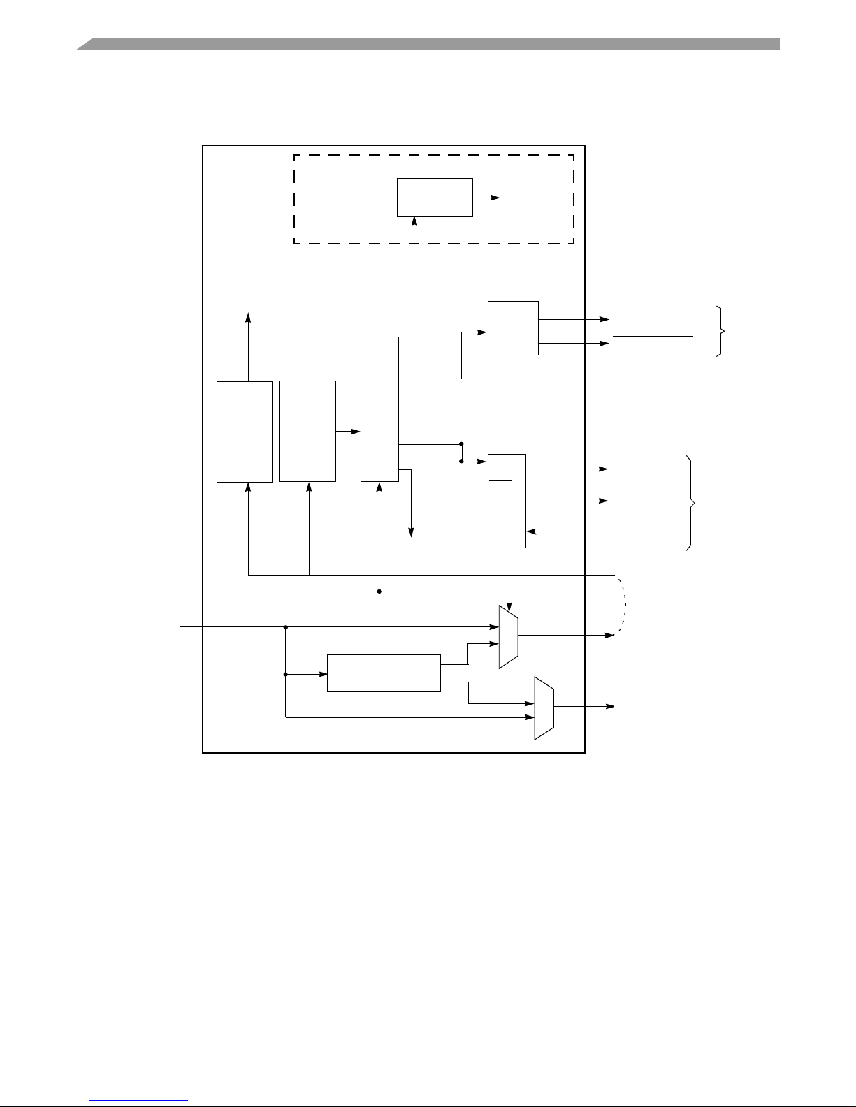
Clocking
Core PLL
System
LBIU
LSYNC_IN
LSYNC_OUT
LCLK[0:2]
core_clk
e300 Core
csb_clk to Rest
CLKIN
csb_clk
MPC8358E
Local Bus
PCI_CLK_OUT[0:2]
PCI_SYNC_OUT
PCI_CLK/
Clock
Unit
of the Device
lb_clk
CFG_CLKIN_DIV
PCI Clock
PCI_SYNC_IN
Memory
Device
/n
DLL
Divider
MEMC1_MCK[0:5]
MEMC1_MCK
[0:5]
DDRC
/2
ddr1_clk
DDRC
Memory
Device
PLL
QUICC
PLL
ce_clk to QUICC Engine Block
Engine
Figure 55 shows the internal distribution of clocks within the MPC8358E.
The primary clock source for the device can be one of two inputs, CLKIN or PCI_CLK, depending on
whether the device is configured in PCI hos t or PCI agent mode. Note that in PCI host mode, the primary
clock input also depends on whether PCI clock outputs are selected with RCWH[PCICKDRV]. When the
device is configured as a PCI host device (RCWH[PCIHOST] = 1) and PCI clock output is selected
(RCWH[PCICKDRV] = 1), CLKIN is its primary input clock. CLKIN feeds the PCI clock divider (÷2)
and the multiplexors for PCI_SYNC_OUT and PCI_CLK_OUT. The CFG_CLKIN_DIV configuration
input selects whether CLKIN or CLKIN/2 is driven out on the PCI_SYNC_OUT signal. The
OCCR[PCIOENn] parameters enable the PCI_CLK_OUTn, respectively.
Figure 55. MPC8358E Clock Subsystem
MPC8360E/MPC8358E PowerQUICC II Pro Processor Revision 2.x TBGA Silicon Hardware Specifications, Rev. 4
86 Freescale Semiconductor
Page 87

Clocking
PCI_SYNC_OUT is connected externally to PCI_SYNC_IN to allow the internal clock subystem to
synchronize to the system PCI clocks. PCI_SYNC_OUT must be connected properly to PCI_SYNC_IN,
with equal delay to all PCI agent devices in the system, to allow the device to function. When the device
is configured as a PCI agent device, PCI_CLK is the primary input clock. When the device is configured
as a PCI agent device the CLKIN and the CFG_CLKIN_DIV signals should be tied to GND.
When the device is configured as a PCI host device (RCWH[PCIHOST] = 1) and PCI clock output is
disabled (RCWH[PCICKDRV] = 0), clock distribution and balancing done externally on the board.
Therefore, PCI_SYNC_IN is the primary input clock.
As shown in Figure 54 and Figure 55, the primary clock input (frequency) is multiplied by the QUICC
Engine block phase-locked loop (PLL), the system PLL, and the clock unit to create the QUICC Engine
clock (ce_clk), the coherent system bus clock (csb_clk), the internal DDRC1 controller clock (ddr1_clk),
and the internal clock for the local bus interface unit and DDR2 memory controller (lb_clk).
The csb_clk frequency is derived from a complex set of factors that can be simplified into the following
equation:
csb_clk = {PCI_SYNC_IN × (1 + CFG_CLKIN_DIV)} × SPMF
In PCI host mode, PCI_SYNC_IN × (1 + CFG_CLKIN_DIV) is the CLKIN frequency; in PCI agent
mode, CFG_CLKIN_DIV must be pulled down (low), so PCI_SYNC_IN × (1 + CFG_CLKIN_DIV) is
the PCI_CLK frequency.
The csb_clk serves as the clock input to the e300 core. A second PLL inside the e300 core multiplies up
the csb_clk frequency to create the internal clock for the e300 core (core_clk). The system and core PLL
multipliers are selected by the SPMF and COREPLL fields in the reset configuration word low (RCWL)
which is loaded at power-on reset or by one of the hard-coded reset options. See Chapter 4, “Reset,
Clocking, and Initialization,” in the MPC8360E PowerQUICC II Pro Integrated Communications
Processor Family Reference Manual for more information on the clock subsystem.
The ce_clk frequency is determined by the QUICC Engine PLL multiplication factor (RCWL[CEPMF)
and the QUICC Engine PLL division factor (RCWL[CEPDF]) according to the following equation:
ce_clk = (primary clock input × CEPMF) ÷ (1 + CEPDF)
The internal ddr1_clk frequency is determined by the following equation:
ddr1_clk = csb_clk × (1 + RCWL[DDR1CM])
Note that the lb_clk clock frequency (for DDRC2) is determined by RCWL[L BCM] . The internal
ddr1_clk frequency is not the external memory bus frequency; ddr1_clk passes through the DDRC1 clock
divider (÷2) to create the differential DDRC1 memory bus clock outputs (MEMC1_MCK and
MEMC1_MCK
). However, the data rate is the same frequency as ddr1_clk.
The internal lb_clk frequency is determined by the following equation:
lb_clk = csb_clk × (1 + RCWL[LBCM])
Note that lb_clk is not the external local bus or DDRC2 frequency; lb_clk passes through the a LB clock
divider to create the external local bus clock outputs (LSYNC_OUT and LCLK[0:2]). The LB clock
divider ratio is controlled by LCRR[CLKDIV].
MPC8360E/MPC8358E PowerQUICC II Pro Processor Revision 2.x TBGA Silicon Hardware Specifications, Rev. 4
Freescale Semiconductor 87
Page 88
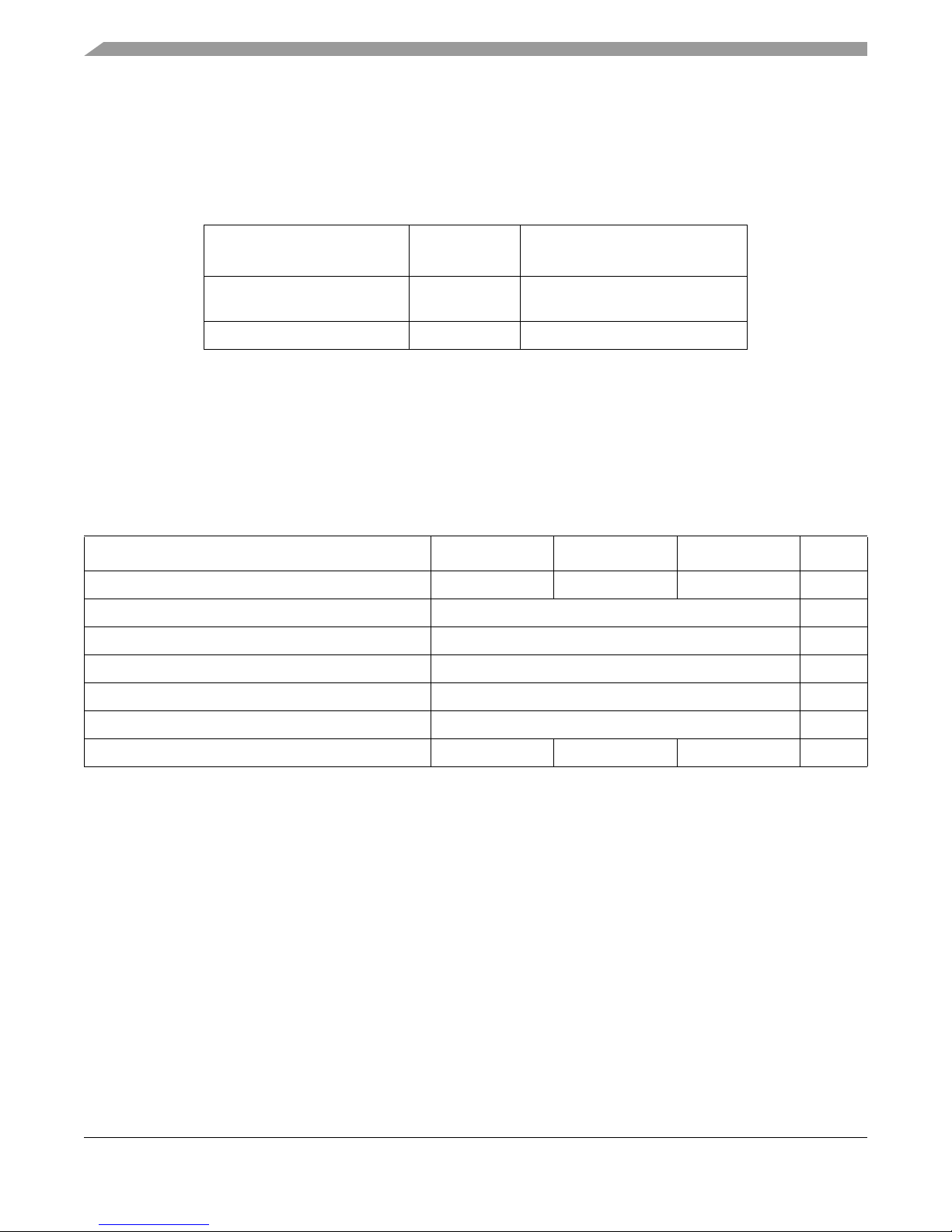
Clocking
In addition, some of the internal units may be required to be shut off or operate at lower frequency than
the csb_clk frequency . Those units have a default clock ratio that can be configured by a memory mapped
register after the device comes out of reset. Table 68 specifies which units have a configurable clock
frequency.
Table 68. Configurable Clock Units
Unit
Security core
Default
Frequency
Options
csb_clk/3 Off, csb_clk1, csb_clk/2,
csb_clk/3
PCI and DMA complex csb_clk Off,
1
With limitation, only for slow csb_clk rates, up to 166 MHz.
csb_clk
Table 69 provides the operating frequencies for the TBGA package under recommended operating
conditions (see Table 2). All frequency combinations shown in the table below may not be available.
Maximum operating frequencies depend on the part ordered, see Section 25.1, “Part Numbers Fully
Addressed by this Document,” for part ordering details and contact your Freescale sales representative or
authorized distributor for more information.
Table 69. Operating Frequencies for the TBGA Package
Characteristic
e300 core frequency (
Coherent system bus frequency (
QUICC Engine frequency
DDR and DDR2 memory bus frequency (MCLK)
Local bus frequency (LCLK
core_clk
3
(
1
) 266–400 266–533 266–667 MHz
csb_clk
) 133–333 MHz
ce_clk
)
5
n
)
400 MHz 533 MHz 667 MHz
266–500 MHz
4
100–166.67 MHz
16.67–133 MHz
2
Unit
PCI input frequency (CLKIN or PCI_CLK) 25–66.67 MHz
Security core maximum internal operating frequency 133 133 166 MHz
1
The CLKIN frequency, RCWL[SPMF], and RCWL[COREPLL] settings must be chosen such that the resulting
LCLK[0:2], and
2
The 667 MHz core frequency is based on a 1.3 V VDD supply voltage.
3
The 500 MHz QE frequency is based on a 1.3 V VDD supply voltage.
4
The DDR data rate is 2x the DDR memory bus frequency.
5
The local bus frequency is 1/2, 1/4, or 1/8 of the
csb_clk
88 Freescale Semiconductor
frequency (depending on RCWL[LBCM]).
MPC8360E/MPC8358E PowerQUICC II Pro Processor Revision 2.x TBGA Silicon Hardware Specifications, Rev. 4
core_clk
frequencies do not exceed their respective maximum or minimum operating frequencies.
lb_clk
frequency (depending on LCRR[CLKDIV]) which is in turn 1× or 2× the
csb_clk
, MCLK,
Page 89
Clocking
22.1 System PLL Configuration
The system PLL is controlled by the RCWL[SPMF] and RCWL[SVCOD] parameters. Table 70 shows the
multiplication factor encodings for the system PLL.
Table 70. System PLL Multiplication Factors
RCWL[SPMF]
0000 × 16
0001 Reserved
0010 × 2
0011 × 3
0100 × 4
0101 × 5
0110 × 6
0111 × 7
1000 × 8
1001 × 9
1010 × 10
1011 × 11
1100 × 12
1101 × 13
1110 × 14
Multiplication Factor
System PLL
1111 × 15
The RCWL[SVCOD] denotes the system PLL VCO internal frequency as shown in Table 71.
Table 71. System PLL VCO Divider
RCWL[SVCOD] VCO Divider
00 4
01 8
10 2
11 Reserved
NOTE
The VCO divider must be set properly s o that the system VCO frequency is
in the range of 600–1400 MHz.
MPC8360E/MPC8358E PowerQUICC II Pro Processor Revision 2.x TBGA Silicon Hardware Specifications, Rev. 4
Freescale Semiconductor 89
Page 90
Clocking
The system VCO frequency is derived from the following equations:
• csb_clk = {PCI_SYNC_IN × (1 + CFG_CLKIN_DIV)} × SPMF
• System VCO Frequency = csb_clk × VCO divider (if both RCWL[DDRCM] and RCWL[LBCM]
are cleared)
OR
• System VCO frequency = 2 × csb_clk × VCO divider (if either RCWL[DDRCM] or
RCWL[LB CM] are set).
As described in Section 22, “Clocking,” the LBCM, DDRCM, and SPMF parameters in the reset
configuration word low and the CFG_CLKIN_DIV configuration input signal select the ratio between the
primary clock input (CLKIN or PCI_CLK) and the internal coherent system bus clock (csb_clk). Table 72
shows the expected frequency values for the CSB frequency for select csb_clk to CLKIN/PCI_SYNC_IN
ratios.
Table 72. CSB Frequency Options
Input Clock Frequency (MHz)
CFG_CLKIN_DIV
at Reset
1
Low 0010 2:1
Low 0011 3:1 100 200
Low 0100 4:1 100 133 266
Low 0101 5:1 125 166 333
Low 0110 6:1 100 150 200
Low 0111 7:1 116 175 233
Low 1000 8:1 133 200 266
Low 1001 9:1 150 225 300
Low 1010 10:1 166 250 333
Low 1011 11:1 183 275
Low 1100 12:1 200 300
Low 1101 13:1 216 325
Low 1110 14:1 233
SPMF
csb_clk
Input Clock Ratio
:
16.67 25 33.33 66.67
2
csb_clk
Frequency (MHz)
2
133
Low 1111 15:1 250
Low 0000 16:1 266
High 0010 2:1
High 0011 3:1 100 200
High 0100 4:1 133 266
High 0101 5:1 166 333
MPC8360E/MPC8358E PowerQUICC II Pro Processor Revision 2.x TBGA Silicon Hardware Specifications, Rev. 4
90 Freescale Semiconductor
133
Page 91
Table 72. CSB Frequency Options (continued)
Clocking
Input Clock Frequency (MHz)
CFG_CLKIN_DIV
at Reset
1
CFG_CLKIN_DIV is only used for host mode; CLKIN must be tied low and CFG_CLKIN_DIV must be pulled down (low) in
agent mode.
2
CLKIN is the input clock in host mode; PCI_CLK is the input clock in agent mode.
1
High 0110 6:1 200
High 0111 7:1 233
High 1000 8:1
High 1001 9:1
High 1010 10:1
High 1011 11:1
High 1100 12:1
High 1101 13:1
High 1110 14:1
High 1111 15:1
High 0000 16:1
SPMF
csb_clk
Input Clock Ratio
:
16.67 25 33.33 66.67
2
csb_clk
Frequency (MHz)
2
22.2 Core PLL Configuration
RCWL[COREPLL] selects the ratio between the internal coherent system bus clock (csb_clk) and the e300
core clock (core_clk). Table 73 shows the encodings for RCWL[COREPLL]. COREPLL values not listed
in Table 73 should be considered reserved.
Table 73. e300 Core PLL Configuration
RCWL[COREPLL]
0–1 2–5 6
nn 0000 n PLL bypassed
00 0001 01:1
01 0001 01:1
10 0001 01:1
11 0001 01:1
00 0001 11.5:1
01 0001 11.5:1
10 0001 11.5:1
core_clk:csb_clk
Ratio
(PLL off,
clocks core directly)
csb_clk
VCO divider
PLL bypassed
(PLL off,
clocks core directly)
csb_clk
÷2
÷4
÷8
÷8
÷2
÷4
÷8
MPC8360E/MPC8358E PowerQUICC II Pro Processor Revision 2.x TBGA Silicon Hardware Specifications, Rev. 4
Freescale Semiconductor 91
Page 92
Clocking
Table 73. e300 Core PLL Configuration (continued)
RCWL[COREPLL]
0–1 2–5 6
11 0001 11.5:1 ÷8
00 0010 02:1
01 0010 02:1
10 0010 02:1
11 0010 02:1
00 0010 12.5:1
01 0010 12.5:1
10 0010 12.5:1
11 0010 12.5:1
00 0011 03:1
01 0011 03:1
10 0011 03:1
11 0011 03:1
core_clk:csb_clk
Ratio
VCO divider
NOTE
÷2
÷4
÷8
÷8
÷2
÷4
÷8
÷8
÷2
÷4
÷8
÷8
Core VCO frequency = Core frequency × VCO divider. The VCO divider
(RCWL[COREPLL[0:1]]) must be set properly so that the core VCO
frequency is in the range of 800–1800 MHz. Having a core frequency below
the CSB frequency is not a possible option because the core frequency must
be equal to or greater than the CSB frequency.
22.3 QUICC Engine Block PLL Configuration
The QUICC Engine block PLL is controlled by the RCWL[CEPMF], RCWL[CEPDF], and
RCWL[CEVCOD] parameters. Table 74 shows the multiplication factor encodings for the QUICC Engine
block PLL.
Table 74. QUICC Engine Block PLL Multiplication Factors
QUICC Engine PLL
RCWL[CEPMF] RCWL[CEPDF]
00000 0 × 16
00001 0 Reserved
00010 0 × 2
00011 0 × 3
Multiplication Factor = RCWL[CEPMF]/
(1 + RCWL[CEPDF])
00100 0 × 4
MPC8360E/MPC8358E PowerQUICC II Pro Processor Revision 2.x TBGA Silicon Hardware Specifications, Rev. 4
92 Freescale Semiconductor
Page 93
Table 74. QUICC Engine Block PLL Multiplication Factors (continued)
QUICC Engine PLL
RCWL[CEPMF] RCWL[CEPDF]
00101 0 × 5
00110 0 × 6
00111 0 × 7
01000 0 × 8
01001 0 × 9
01010 0 × 10
01011 0 × 11
01100 0 × 12
01101 0 × 13
01110 0 × 14
01111 0 × 15
10000 0 × 16
Multiplication Factor = RCWL[CEPMF]/
(1 + RCWL[CEPDF])
Clocking
10001 0 × 17
10010 0 × 18
10011 0 × 19
10100 0 × 20
10101 0 × 21
10110 0 × 22
10111 0 × 23
11000 0 × 24
11001 0 × 25
11010 0 × 26
11011 0 × 27
11100 0 × 28
11101 0 × 29
11110 0 × 30
11111 0 × 31
00011 1 × 1.5
00101 1 × 2.5
00111 1 × 3.5
01001 1 × 4.5
MPC8360E/MPC8358E PowerQUICC II Pro Processor Revision 2.x TBGA Silicon Hardware Specifications, Rev. 4
Freescale Semiconductor 93
Page 94
Clocking
Table 74. QUICC Engine Block PLL Multiplication Factors (continued)
QUICC Engine PLL
RCWL[CEPMF] RCWL[CEPDF]
01011 1 × 5.5
01101 1 × 6.5
01111 1 × 7.5
10001 1 × 8.5
10011 1 × 9.5
10101 1 × 10.5
10111 1 × 11.5
11001 1 × 12.5
11011 1 × 13.5
11101 1 × 14.5
Note:
1. Reserved modes are not listed.
Multiplication Factor = RCWL[CEPMF]/
(1 + RCWL[CEPDF])
The RCWL[CEVCOD] denotes the QUICC Engine Block PLL VCO internal frequency as shown in
Table 75.
Table 75. QUICC Engine Block PLL VCO Divider
RCWL[CEVCOD] VCO Divider
00 4
01 8
10 2
11 Reserved
NOTE
The VCO divider (RCWL[CEVCOD]) must be set properly so that the
QUICC Engine block VCO frequency is in the range of 600–1400 MHz.
The QUICC Engine block frequency is not restricted by the CSB and core
frequencies. The CSB, core, and QUICC Engine block frequencies should
be selected according to the performance requirements.
The QUICC Engine block VCO frequency is derived from the following equations:
ce_clk = (primary clock input × CEPMF) ÷ (1 + CEPDF)
QE VCO Frequency = ce_clk × VCO divider × (1 + CEPDF)
MPC8360E/MPC8358E PowerQUICC II Pro Processor Revision 2.x TBGA Silicon Hardware Specifications, Rev. 4
94 Freescale Semiconductor
Page 95
Clocking
22.4 Suggested PLL Configurations
To simplify the PLL configurations, the device might be separated into two clock domains. The first
domain contains the CSB PLL and the core PL L. The core PLL is connected seri ally to the CSB PLL, and
has the csb_clk as its input clock. The second clock domain has the QUICC Engine block PLL. The clock
domains are independent, and each of their PLLs are configured separately. Both of the domains has one
common input clock. Table 76 shows suggested PLL configurations for 33 and 66 MHz input clocks and
illustrates each of the clock domains separately. Any combination of clock domains setting with same
input clock are valid. Refer to Section 22, “Clocking,” for the appropriate operating frequencies for your
device.
Table 76. Suggested PLL Configurations
Conf
No.
SPMF
1
CORE
PLL
CEPMF CEPDF
33 MHz CLKIN/PCI_SYNC_IN Options
Input
Clock Freq
(MHz)
CSB Freq
(MHz)
Core Freq
(MHz)
QUICC
Engine
Freq (MHz)
400
(MHz)
533
(MHz)
667
(MHz)
s1
s2
s3
s4
s5
s6
s7
s8
s9
s10
s11
s12
s13
s14
s15
s16
s17
0100 0000100 æ æ 33 133 266 — ∞∞∞
0100 0000101 æ æ 33 133 333 — ∞∞∞
0101 0000100 æ æ 33 166 333 — ∞∞∞
0101 0000101 æ æ 33 166 416 — — ∞∞
0110 0000100 æ æ 33 200 400 — ∞∞∞
0110 0000110 æ æ 33 200 600 — — — ∞
0111 0000011 æ æ 33 233 350 — ∞∞∞
0111 0000100 æ æ 33 233 466 — —
0111 0000101 æ æ 33 233 583 — — — ∞
1000 0000011 æ æ 33 266 400 — ∞∞∞
1000 0000100 æ æ 33 266 533 — — ∞∞
1000 0000101 æ æ 33 266 667 — — — ∞
1001 0000010 æ æ 33 300 300 — ∞∞∞
1001 0000011 æ æ 33 300 450 — — ∞∞
1001 0000100 æ æ 33 300 600 — — — ∞
1010 0000010 æ æ 33 333 333 — ∞∞∞
1010 0000011 æ æ 33 333 500 — — ∞∞
∞∞
s18
c1
c2
c3
c4
Freescale Semiconductor 95
1010 0000100 æ æ 33 333 667 — — — ∞
æ æ 01001 0 33 — — 300 ∞∞ ∞
æ æ 01100 0 33 — — 400 ∞∞ ∞
æ æ 01110 0 33 — — 466 — ∞∞
æ æ 01111 0 33 — — 500 — ∞∞
MPC8360E/MPC8358E PowerQUICC II Pro Processor Revision 2.x TBGA Silicon Hardware Specifications, Rev. 4
Page 96
Clocking
Table 76. Suggested PLL Configurations (continued)
Conf
No.
SPMF
1
c5 æ æ 10000 0 33 — — 533 — ∞∞
CORE
PLL
CEPMF CEPDF
Input
Clock Freq
(MHz)
CSB Freq
(MHz)
Core Freq
(MHz)
QUICC
Engine
Freq (MHz)
400
(MHz)
533
(MHz)
667
(MHz)
c6
s1h 0011 0000110
s2h 0011 0000101
s3h 0011 0000110
s4h 0100 0000011
s5h 0100 0000100
s6h 0100 0000101
s7h 0101 0000010
s8h 0101 0000011
s9h 0101 0000100
c1h
c2h
c3h
c4h
c5h
1
The Conf No. consist of prefix, an index and a postfix. The prefix “s” and “c” stands for “syset” and “ce” respectively. The postfix
“h” stands for “high input clock.’”The index is a serial number.
æ æ 10001 0 33 — — 566 — — ∞
66 MHz CLKIN/PCI_SYNC_IN Options
æ æ 66 200 400 — ∞∞∞
æ æ 66 200 500 — — ∞∞
æ æ 66 200 600 — — — ∞
æ æ 66 266 400 — ∞∞∞
æ æ 66 266 533 — — ∞∞
æ æ 66 266 667 — — — ∞
æ æ 66 333 333 — ∞∞∞
æ æ 66 333 500 — — ∞∞
æ æ 66 333 667 — — — ∞
æ æ 00101 0 66 — — 333 ∞∞ ∞
æ æ 00110 0 66 — — 400 ∞∞ ∞
æ æ 00111 0 66 — — 466 — ∞∞
æ æ 01000 0 66 — — 533 — ∞∞
æ æ 01001 0 66 — — 600 — — ∞
The following steps describe how to use Table 76. See Example 1.
1. Choos e the up or down sections in the table according to input clock rate 33 MHz or 66 MHz.
2. Select a suitable CSB and core clock rates from Table 76. Copy the SPMF and CORE PLL
configuration bits.
3. Select a suitable QUICC Engine block clock rate from Table 76. Copy the CEPMF and CEPDF
configuration bits.
4. Ins er t the chosen SPMF, COREPLL, CEPMF and CEPDF to the RCWL fields, respectivel y.
MPC8360E/MPC8358E PowerQUICC II Pro Processor Revision 2.x TBGA Silicon Hardware Specifications, Rev. 4
96 Freescale Semiconductor
Page 97
Example 1. Sample Table Use
Thermal
Index SPMF
A
1000 0000011 01001 0 33 266 400 300 ∞∞ ∞
B 0100 0000100 00110 0 66 266 533 400 ∞∞∞
CORE
PLL
CEPMF CEPDF
Input Clock
(MHz)
CSB Freq
(MHz)
Core Freq
(MHz)
QUICC
Engine Freq
(MHz)
400
(MHz)
533
(MHz)
667
(MHz)
• Example A. To configure the device with CSB clock rate of 266 MHz, core rate of 400 MHz, and
QUICC Engine clock rate 300 MHz while the input clock rate is 33 MHz. Conf No. ‘s10’ and ‘c1’
are selected from Table 76. SPMF is 1000, CORPLL is 0000011, CEPMF is 01001, and CEPDF
is 0.
• Example B. T o configure the device with CSBCSB clock rate of 266 MHz, core rate of 533 MHz
and QUICC Engine clock rate 400 MHz while the input clock rate is 66 MHz. Conf No. ‘s5h’ and
‘c2h’ are selected from Table 76. SPMF is 0100, CORPLL is 0000100, CEPMF is 00110, and
CEPDF is 0.
23 Thermal
This section describes the thermal specifications of the MPC8360E/58E.
23.1 Thermal Characteristics
Table 77 provides the package thermal characteristics for the 37.5 mm × 37.5 mm 740-TBGA package.
Table 77. Package Thermal Characteristics for the TBGA Package
Characteristic Symbol Value Unit Notes
Junction-to-ambient natural convection on single-layer board (1s) R
Junction-to-ambient natural convection on four-layer board (2s2p) R
Junction-to-ambient (@1 m/s) on single-layer board (1s) R
Junction-to-ambient (@ 1 m/s) on four-layer board (2s2p) R
Junction-to-ambient (@ 2 m/s) on single-layer board (1s) R
Junction-to-ambient (@ 2 m/s) on four-layer board (2s2p) R
Junction-to-board thermal R
Junction-to-case thermal R
θJA
θJA
θJMA
θJMA
θJMA
θJMA
θJB
θJC
15 °C/W 1, 2
11 °C/W 1, 3
10 °C/W 1, 3
8 °C/W 1, 3
9 °C/W 1, 3
7 °C/W 1, 3
4.5 °C/W 4
1.1 °C/W 5
MPC8360E/MPC8358E PowerQUICC II Pro Processor Revision 2.x TBGA Silicon Hardware Specifications, Rev. 4
Freescale Semiconductor 97
Page 98
Thermal
Table 77. Package Thermal Characteristics for the TBGA Package (continued)
Characteristic Symbol Value Unit Notes
Junction-to-package natural convection on top ψ
Notes
1. Junction temperature is a function of die size, on-chip power dissipation, package thermal resistance, mounting site (board)
temperature, ambient temperature, airflow, power dissipation of other components on the board, and board thermal
resistance.
2. Per JEDEC JESD51-2 and SEMI G38-87 with the single layer board horizontal.
3. Per JEDEC JESD51-6 with the board horizontal. 1 m/sec is approximately equal to 200 linear feet per minute (LFM).
4. Thermal resistance between the die and the printed-circuit board per JEDEC JESD51-8. Board temperature is measured on
the top surface of the board near the package.
5. Thermal resistance between the die and the case top surface as measured by the cold plate method (MIL SPEC-883 Method
1012.1).
6. Thermal characterization parameter indicating the temperature difference between package top and the junction temperature
per JEDEC JESD51-2. When Greek letters are not available, the thermal characterization parameter is written as Psi-JT.
JT
1 °C/W 6
23.2 Thermal Management Information
For the following sections, PD = (VDD× IDD) + P
See Table 6 for typical power dissipations values.
23.2.1 Estimation of Junction Temperature with Junction-to-Ambient
Thermal Resistance
An estimation of the chip junction temperature, TJ, can be obtained from the equation:
where P
I/O
is the p ower dissipation of the I/O drivers.
I/O
TJ = TA + (R
θ
JA
× PD)
where:
TJ = junction temperature (°C)
TA = ambient temperature for the package (°C)
R
= junction-to-ambient thermal resistance (°C/W)
θ
JA
= power dissipation in the package (W)
P
D
The junction-to-ambient thermal resistance is an industry standard value that provides a quick and easy
estimation of thermal performance. As a general statement, the value obtained on a single-layer board is
appropriate for a tightly packed printed-circuit board. The value obtained on the board with the internal
planes is usually appropriate if the board has low power dissipation and the components are well separated.
Test cases have demonstrated that errors of a factor of two (in the quantity T
– TA) are possible.
J
23.2.2 Estimation of Junction Temperature with Junction-to-Board
Thermal Resistance
The thermal performance of a device cannot be adequately predicted from the junction-to-ambient thermal
resistance. The thermal performance of any component is strongly dependent on the power dissipation of
surrounding components. In addition, the ambient temperature varies widely within the application. For
many natural convection and especially closed box applications, the board temperature at the perimeter
MPC8360E/MPC8358E PowerQUICC II Pro Processor Revision 2.x TBGA Silicon Hardware Specifications, Rev. 4
98 Freescale Semiconductor
Page 99

Thermal
(edge) of the package will be approximately the same as the local air temperature near the device.
Specifying the local ambient conditions explicitly as the board temperature provides a more precise
description of the local ambient conditions that determine the temperature of the device. At a known board
temperature, the junction temperature is estimated using the following equation:
TJ = TB + (R
θ
JB
× PD)
where:
TJ = junction temperature (°C)
TB = board temperature at the package perimeter (°C)
= junction to board thermal resistance (°C/W) per JESD51-8
R
θ
JA
P
= power dissipation in the package (W)
D
When the heat loss from the package case to the air can be ignored, acceptable predictions of junction
temperature can be made. The application board should be similar to the thermal test condition: the
component is soldered to a board with internal planes.
23.2.3 Experimental Determination of Junction Temperature
To determine the junction temperature of the device in the application after prototypes are available, the
Thermal Characterization Parameter (ΨJT) can be used to determine the junction temperature with a
measurement of the temperature at the top center of the package case using the following equation:
TJ = TT + (
where:
TJ = junction temperature (°C)
Ψ
× PD)
JT
TT = thermocouple temperature on top of package (°C)
Ψ
= junction-to-ambient thermal resistance (°C/W)
JT
PD = power dissipation in the package (W)
The thermal characterization parameter is measured per JESD51-2 specification using a 40 gauge type T
thermocouple epoxied to the top center of the package case. The thermocouple should be positioned so
that the thermocouple junction rests on the package. A small amount of epoxy is placed over the
thermocouple junction and over about 1 mm of wire extending from the junction. The thermocouple wire
is placed flat against the package case to avoid measurement errors caused by cooling effects of the
thermocouple wire.
23.2.4 Heat Sinks and Junction-to-Ambient Thermal Resistance
In some application environments, a heat sink will be required to provide the necessary thermal
management of the device. When a heat sink is used, the thermal resistance is expressed as the sum of a
junction to case thermal resistance and a case to ambient thermal resistance:
R
where:
= R
θ
JA
R
= junction-to-ambient thermal resistance (°C/W)
θ
JA
+ R
θ
JC
θ
CA
MPC8360E/MPC8358E PowerQUICC II Pro Processor Revision 2.x TBGA Silicon Hardware Specifications, Rev. 4
Freescale Semiconductor 99
Page 100
Thermal
R
= junction-to-case thermal resistance (°C/W)
θ
JC
R
= case-to-ambient thermal resistance (°C/W)
θ
CA
is device related and cannot be influenced by the user. The user controls the thermal environment to
R
θ
JC
change the case-to-ambient thermal resistance, R
. For instance, the user can change the size of the heat
θ
CA
sink, the airflow around the device, the interface material, the mounting arrangement on printed-circuit
board, or change the thermal dissipation on the printed-circuit board surrounding the device.
To illustrate the thermal performance of the devices with heat sinks, the thermal performance has been
simulated with a few commercially available heat sinks. The heat sink choice is determined by the
application environment (temperature, airflow, adjacent component power dissipation) and the physical
space available. Because there is not a standard application environment, a standard heat sink is not
required.
Table 78 shows heat sinks and junction-to-ambient thermal resistance for TBGA package.
Table 78. Heat Sinks and Junction-to-Ambient Thermal Resistance of TBGA Package
35 × 35 mm TBGA
Heat Sink Assuming Thermal Grease Airflow
Junction-to-Ambient
Thermal Resistance
AAVID 30 × 30 × 9.4 mm pin fin Natural convention 10.7
AAVID 30 × 30 × 9.4 mm pin fin 1 m/s 6.2
AAVID 30 × 30 × 9.4 mm pin fin 2 m/s 5.3
AAVID 31 × 35 × 23 mm pin fin Natural convention 8.1
AAVID 31 × 35 × 23 mm pin fin 1 m/s 4.4
AAVID 31 × 35 × 23 mm pin fin 2 m/s 3.7
Wakefield, 53 × 53 × 25 mm pin fin Natural convention 5.4
Wakefield, 53 × 53 × 25 mm pin fin 1 m/s 3.2
Wakefield, 53 × 53 × 25 mm pin fin 2 m/s 2.4
MEI, 75 × 85 × 12 no adjacent board, extrusion Natural convention 6.4
MEI, 75 × 85 × 12 no adjacent board, extrusion 1 m/s 3.8
MEI, 75 × 85 × 12 no adjacent board, extrusion 2 m/s 2.5
MEI, 75 × 85 × 12 mm, adjacent board, 40 mm side bypass 1 m/s 2.8
Accurate thermal design requires thermal modeling of the application environment using computational
fluid dynamics software which can model both the conduction cooling and the convection cooling of the
air moving through the application. Simplified ther mal models of the packages can be assembled using the
junction-to-case and junction-to-board thermal resi stanc es listed in the thermal resistance table. More
detailed thermal models can be made available on request.
MPC8360E/MPC8358E PowerQUICC II Pro Processor Revision 2.x TBGA Silicon Hardware Specifications, Rev. 4
100 Freescale Semiconductor
 Loading...