

Page 1

MPC8349E MDS Processor Board
User Manual
Rev. 1.6
12/2005
Page 2

ii Freescale Semiconductor
MPC8349E MDS Processor Board, Rev. 1.6
Page 3

Section 1
General Information
1.1 Introduction . . . . . . . . . . . . . . . . . . . . . . . . . . . . . . . . . . . . . . . . . . . . . . . . . . . . . . . . . . . . 7
1.1.1 MPC8349E MDS Processor Board . . . . . . . . . . . . . . . . . . . . . . . . . . . . . . . . . . . . 7
1.1.2 Working Configurations . . . . . . . . . . . . . . . . . . . . . . . . . . . . . . . . . . . . . . . . . . . . 8
1.1.2.1 Stand-Alone: . . . . . . . . . . . . . . . . . . . . . . . . . . . . . . . . . . . . . . . . . . . . . . . 8
1.1.2.2 With PIB board (PIB Combined Mode): . . . . . . . . . . . . . . . . . . . . . . . . . . 8
1.1.2.3 PCI Add-On (Agent Mode): . . . . . . . . . . . . . . . . . . . . . . . . . . . . . . . . . . . 8
1.2 Definitions, Acronyms, and Abbreviations . . . . . . . . . . . . . . . . . . . . . . . . . . . . . . . . . . . . 9
1.3 Related Documentation . . . . . . . . . . . . . . . . . . . . . . . . . . . . . . . . . . . . . . . . . . . . . . . . . . 10
1.4 Specifications . . . . . . . . . . . . . . . . . . . . . . . . . . . . . . . . . . . . . . . . . . . . . . . . . . . . . . . . . . 10
1.5 MPC8349E MDS Processor Board Features . . . . . . . . . . . . . . . . . . . . . . . . . . . . . . . . . . 11
1.6 External Connections . . . . . . . . . . . . . . . . . . . . . . . . . . . . . . . . . . . . . . . . . . . . . . . . . . . . 12
1.7 Block Diagram . . . . . . . . . . . . . . . . . . . . . . . . . . . . . . . . . . . . . . . . . . . . . . . . . . . . . . . . . 14
Section 2
Hardware Preparation and Installation
2.1 Unpacking Instructions . . . . . . . . . . . . . . . . . . . . . . . . . . . . . . . . . . . . . . . . . . . . . . . . . . 15
2.2 Installation Instructions . . . . . . . . . . . . . . . . . . . . . . . . . . . . . . . . . . . . . . . . . . . . . . . . . . 15
2.2.1 Stand-Alone Mode . . . . . . . . . . . . . . . . . . . . . . . . . . . . . . . . . . . . . . . . . . . . . . . . 16
2.2.3 For Agent Mode only : . . . . . . . . . . . . . . . . . . . . . . . . . . . . . . . . . . . . . . . . . . . . . 25
Section 3
Memory Map
3.1 MPC8349E MDS Processor Board Mapping . . . . . . . . . . . . . . . . . . . . . . . . . . . . . . . . . 27
Section 4
Controls and Indicators
4.1 Switches and Jumpers Locations . . . . . . . . . . . . . . . . . . . . . . . . . . . . . . . . . . . . . . . . . . . 29
4.1.1 Switches . . . . . . . . . . . . . . . . . . . . . . . . . . . . . . . . . . . . . . . . . . . . . . . . . . . . . . . . 30
4.1.2 Jumpers . . . . . . . . . . . . . . . . . . . . . . . . . . . . . . . . . . . . . . . . . . . . . . . . . . . . . . . . 30
4.2 LEDs . . . . . . . . . . . . . . . . . . . . . . . . . . . . . . . . . . . . . . . . . . . . . . . . . . . . . . . . . . . . . . . . 30
4.2.1 LD1, LD2 - Signaling LEDs . . . . . . . . . . . . . . . . . . . . . . . . . . . . . . . . . . . . . . . . 30
4.2.2 LD3 - USB Power . . . . . . . . . . . . . . . . . . . . . . . . . . . . . . . . . . . . . . . . . . . . . . . . 30
4.2.3 LD4, LD5 - GETH Enable . . . . . . . . . . . . . . . . . . . . . . . . . . . . . . . . . . . . . . . . . . 30
4.2.4 LD6 - DUART Enable . . . . . . . . . . . . . . . . . . . . . . . . . . . . . . . . . . . . . . . . . . . . . 30
4.2.5 LD7 - FUNC Indication . . . . . . . . . . . . . . . . . . . . . . . . . . . . . . . . . . . . . . . . . . . . 30
4.2.6 LD8 - Power GOOD . . . . . . . . . . . . . . . . . . . . . . . . . . . . . . . . . . . . . . . . . . . . . . 30
4.2.7 LD9 - GPIO1-1 Indication . . . . . . . . . . . . . . . . . . . . . . . . . . . . . . . . . . . . . . . . . . 30
Freescale Semiconductor MPC8349E MDS Processor Board User’s Manual 3
Page 4

4.2.8 LD10, LD11 - PCTL0,1 USB . . . . . . . . . . . . . . . . . . . . . . . . . . . . . . . . . . . . . . . 30
4.2.9 LD12 - BOOT Indicator . . . . . . . . . . . . . . . . . . . . . . . . . . . . . . . . . . . . . . . . . . . 30
4.2.10 LD13 - 5V Power Indicator . . . . . . . . . . . . . . . . . . . . . . . . . . . . . . . . . . . . . . . . . 31
4.3 Other Controls and Indicators . . . . . . . . . . . . . . . . . . . . . . . . . . . . . . . . . . . . . . . . . . . . . 31
Section 5
Functional Description
5.1 Reset & Reset - Configuration . . . . . . . . . . . . . . . . . . . . . . . . . . . . . . . . . . . . . . . . . . . . . 33
5.1.1 Power - On Reset . . . . . . . . . . . . . . . . . . . . . . . . . . . . . . . . . . . . . . . . . . . . . . . . . 33
5.1.2 Hard Reset . . . . . . . . . . . . . . . . . . . . . . . . . . . . . . . . . . . . . . . . . . . . . . . . . . . . . . 33
5.1.2.1 COP/JTAG Port Hard - Reset (stand-alone only) . . . . . . . . . . . . . . . . . . 34
5.1.2.2 Manual Hard Reset . . . . . . . . . . . . . . . . . . . . . . . . . . . . . . . . . . . . . . . . . 34
5.1.2.3 Manual Soft Reset . . . . . . . . . . . . . . . . . . . . . . . . . . . . . . . . . . . . . . . . . . 34
5.2 Board Control & Status Registers – BCSR . . . . . . . . . . . . . . . . . . . . . . . . . . . . . . . . . . . 34
5.2.1 BCSR0 - Board Control / Status Register 0 . . . . . . . . . . . . . . . . . . . . . . . . . . . . . 35
5.2.2 BCSR1 - Board Control / Status Register 1 . . . . . . . . . . . . . . . . . . . . . . . . . . . . . 36
5.2.3 BCSR2 - Board Control / Status Register 2 . . . . . . . . . . . . . . . . . . . . . . . . . . . . . 37
5.2.4 BCSR3 - Board Control / Status Register 3 . . . . . . . . . . . . . . . . . . . . . . . . . . . . . 37
5.2.5 BCSR4 - Board Control / Status Register 4 . . . . . . . . . . . . . . . . . . . . . . . . . . . . . 38
5.2.6 BCSR5 - Board Control / Status Register 5 . . . . . . . . . . . . . . . . . . . . . . . . . . . . . 40
5.2.7 BCSR6 - Board Misc. Register 1 . . . . . . . . . . . . . . . . . . . . . . . . . . . . . . . . . . . . . 41
5.2.8 BCSR7 - Board Misc. Register 2 . . . . . . . . . . . . . . . . . . . . . . . . . . . . . . . . . . . . . 41
5.2.9 BCSR8 - Board Misc. Register 3 . . . . . . . . . . . . . . . . . . . . . . . . . . . . . . . . . . . . . 42
5.2.10 BCSR10 - Board Status Register 1 . . . . . . . . . . . . . . . . . . . . . . . . . . . . . . . . . . . 43
5.2.11 BCSR11 - Board Status Register 2 . . . . . . . . . . . . . . . . . . . . . . . . . . . . . . . . . . . 43
5.2.12 CCR - COP Control Register . . . . . . . . . . . . . . . . . . . . . . . . . . . . . . . . . . . . . . . . 44
5.3 External Connections . . . . . . . . . . . . . . . . . . . . . . . . . . . . . . . . . . . . . . . . . . . . . . . . . . . . 45
5.3.1 P1 - MiniAB USB Connector . . . . . . . . . . . . . . . . . . . . . . . . . . . . . . . . . . . . . . . 45
5.3.2 P2 - DUART Port . . . . . . . . . . . . . . . . . . . . . . . . . . . . . . . . . . . . . . . . . . . . . . . . 45
5.3.3 Logic Analyzer Connectors . . . . . . . . . . . . . . . . . . . . . . . . . . . . . . . . . . . . . . . . . 46
5.3.4 P5 - SMB Connector . . . . . . . . . . . . . . . . . . . . . . . . . . . . . . . . . . . . . . . . . . . . . . 46
5.3.5 P9 - Debug COP Connector . . . . . . . . . . . . . . . . . . . . . . . . . . . . . . . . . . . . . . . . . 46
5.3.6 P10 - FPGA’s In-System-Programming (ISP) . . . . . . . . . . . . . . . . . . . . . . . . . . . 48
5.3.7 P11 - Power Connector . . . . . . . . . . . . . . . . . . . . . . . . . . . . . . . . . . . . . . . . . . . . 48
5.3.8 J1,J2 - Ethernet Port Connector . . . . . . . . . . . . . . . . . . . . . . . . . . . . . . . . . . . . . . 49
Section 6
Clocking for the MPC8349E MDS Processor Board
6.1 MPC8349 as Host Device . . . . . . . . . . . . . . . . . . . . . . . . . . . . . . . . . . . . . . . . . . . . . . . . 51
6.2 MPC8349 as Agent . . . . . . . . . . . . . . . . . . . . . . . . . . . . . . . . . . . . . . . . . . . . . . . . . . . . . 52
4 MPC8349E MDS Processor Board User’s Manual Freescale Semiconductor
Page 5

Section 7
Replacing Devices
7.1 Replacing Flash Memory . . . . . . . . . . . . . . . . . . . . . . . . . . . . . . . . . . . . . . . . . . . . . . . . . 53
7.1.1 Cleaning Flash Memory . . . . . . . . . . . . . . . . . . . . . . . . . . . . . . . . . . . . . . . . . . . . 55
7.2 Replacing SODIMM units . . . . . . . . . . . . . . . . . . . . . . . . . . . . . . . . . . . . . . . . . . . . . . . . 56
7.3 Replacing MSC8349E Processor . . . . . . . . . . . . . . . . . . . . . . . . . . . . . . . . . . . . . . . . . . . 58
Freescale Semiconductor MPC8349E MDS Processor Board User’s Manual 5
Page 6

6 MPC8349E MDS Processor Board User’s Manual Freescale Semiconductor
Page 7

General Information
General Information
1.1 Introduction
This document describes the MPC8349E MDS Processor Board, in its stand-alone operating
mode, in addition to its operating mode via a PCI slot in a PC, or its operating mode on the
“PowerQUICC MDS Platform I/O Board (PIB)”.
1.1.1 MPC8349E MDS Processor Board
The MPC8349E MDS Processor Board is an ADS that provides a complete debugging
environment for engineers developing applications for the MPC8349 series of Freescale
processors.
1
The MPC8349E is a cost-effective, general purpose integrated host processor that implements the
PowerPC™ architecture required for networking infrastructure, telecommunications, Wireless
LANs, and other embedded applications. The MPC8349E can also be used for control processing
in applications such as network routers and switches, mass storage subsystems, network
appliances, and print and imaging systems.
The MPC8349E MDS Processor Board includes various peripherals, such as data input/output
devices (GETH, USB, DUART), memories (DDR, SDRAM (optional), Serial EEPROM,
PSRAM (optional) & FLASH and BCSR’s registers), and control switches and LED indicators.
Using its on-board resources and debugging devices, a developer is able to upload code, run the
code, set breakpoints, display memory & registers and connect his own proprietary hardware to
be incorporated into a target system that uses the MPC8349E as a processor.
The software application developed for the MPC8349 can be run in a "bare bones" operation
(with only the MPC8349 processor), or with various input or output data streams, such as from
the GETH connection, PCI or the USB connections. Results can be analyzed using the Code
War ri or
data stream. The BSP is built using the Linux OS.
This board can also be used as a demonstration tool for the developer. For instance, the
developer's application software may be programmed into its Flash memory and run in
exhibitions.
®
debugger in addition to using other methods for directly analyzing the input or output
Freescale Semiconductor MPC8349E MDS Processor Board User’s Manual 7
Page 8

General Information
1.1.2 Working Configurations
1.1.2.1 Stand-Alone:
The MPC8349E MDS Processor Board can be run in a stand-alone mode, like other ADS’s, with
direct connections to deubggers (via a JTAG/COP connector and JTAG/Parallel Port command
converter), power supply, and the GETH, MiniAB USB and Dual RS-232 (DUART) connections.
In this mode, the MPC8349E MDS Processor Board acts as a Host.
1.1.2.2 With PIB board (PIB Combined Mode):
The MPC8349E MDS Processor Board can be connected to the PIB, which allows it to be used in
a back plane, and provides room and connections for an additional USB board, and up to three
additional PCI cards. Each of the PCI cards provides a connection interface for an optional
additional processor board (from the MPC83xx family). This capability allows the MPC8349
processor on the MPC8349E MDS Processor Board to act as a master for up to three “slave”
processors in the MPC83xx family. In this mode, the MPC8349E MDS Processor Board acts as a
Host.
Voltage is provided by the PIB, which also provides additional signal connections via the back
plane (if used), and optical GETH connectors on the front plane side of the PIB. The MPC8349E
MDS Processor Board can be connected to a PC in this configuration (via a parallel port
connector), without needing an external command converter.
1.1.2.3 PCI Add-On (Agent Mode):
Using its PCI edge connector, the MPC8349E MDS Processor Board can be inserted in a PC.
Power and debugging are supplied from the PC (no command converter necessary). Other
external connections are the same as in the Stand-Alone Mode. In this mode, the MPC8349E
MDS Processor Board acts as an Agent.
8 MPC8349E MDS Processor Board User’s Manual Freescale Semiconductor
Page 9

General Information
1.2 Definitions, Acronyms, and Abbreviations
ADS Application Development System
BCSR Board Control and Status Register
BRD Board Revision Detect (I2C EEPROM)
BSP Board Support Package
CCR COP Control Register (FPGA)
COP Common On-chip Processor (JTAG Debug Port)
CS Chip Select
CW
DAC Digital-to-Analog Converter
DDR Double Data Rate
DIP Dual-In-Line Package.
DMA Direct Memory Access
DUART Dual UART
EEPROM Electrical Eraseable Programmable Memory
FCFG Flash Configuration Select
FCI Type of Riser Connector
FLASH Non volatile reprogrammable memory.
FPGA Field-Programmable Gate Array
GbE Gigabit Ethernet
GETH Gigabit Ethernet
GPCM General Purpose Chip-select Machine
GPL General Purpose Line
Metrowerks Code Warrior
®
IDE for PowerPC
I2C Philips Semi Serial Bus
LED Light Emitting Diode
lsb least significant bit
MII Media Independent Interface
GMII General Media Independent Interface
JTAG Joint Test Access Group
OTG On-the-Go
PC IBM-compatible Personal Computer
Freescale Semiconductor MPC8349E MDS Processor Board User’s Manual 9
Page 10

General Information
PCI Peripheral Components Interconnect
Phy Physical Layer
PIB Platform I/O Board - expands the ADS functionality.
PSRAM Pseudo-Static Random Access Memory
PSU Power Supply Unit
RCWL,
RCWH
RGMII Reduced General Media Independent Interface
RTC Real Time Clock
SDRAM Synchronous Dynamic Random Access Memory
SMB Type of Mini-RF connector
SODIMM Mini DIMM Form Factor
SPD Serial Present Detect
TBD To Be Defined
TSEC Triple Speed Ethernet Controller
ULPI UTMI+ Low Pin Interface
UPM User Programmable Machine
USB Universal Serial Bus
ZD Zero Delay clock buffer, with internal PLL for skew elimination
Reset Configuration Word Low/High
1.3 Related Documentation
• MPC8349 HW Specification
• MPC8349 User’s Manual
• PowerQUICC MDS Platform I/O Board User’s Manual
• MPC8349 Getting Started
1.4 Specifications
The MPC8349E MDS Processor Board specifications are given in Table 1-1.
10 MPC8349E MDS Processor Board User’s Manual Freescale Semiconductor
Page 11

General Information
Table 1-1. MPC8349E MDS Processor Board specifications
CHARACTERISTICS SPECIFICATIONS
Power requirements 5V @ 3A external DC power supply (Stand-Alone
Mode). No extra power supply for Agent Mode &
PIB Combined Mode.
In the case of the Agent Mode, power is supplied
by the PC; In the PIB Combined Mode (a Host
mode), either an external power supply provides
power, OR power is supplied from the back plane
connection.
MPC8349E processor Internal clock runs up to 667MHz @ 1.2V
Memory:
DDR: 256MB space 64bit wide in one SODIMM-200 .
Data rate 333MHz.
Local Bus:
SDRAM (Optional) 64MB space 32bit wide + 4bit parity implemented
in three SDRAM parts. 133MHz clock.
Buffered Memory (Flash on socket): 8MB space 16bits wide.
PSRAM (optional) 4MB space 16bits wide, use for Flash emulation.
BCSR on FPGA 16-registers, 8bits wide.
Expansion Four banks with 16bit- Address bus, 16bit- Data
bus
Operating temperature 0
Storage temperature -25
Relative humidity 5% to 90% (non-condensing)
Dimensions (according to PCI 64-bit Add-in-card
form factor):
Length
Width
Height
O
C - 70OC
O
C to 85OC
285 mm
106 mm
16 mm
1.5 MPC8349E MDS Processor Board Features
• Supports MPC8349 running up to 667MHz at 1.2V Core voltage.
• DDR-1 333MHz on SODIMM. Second SODIMM is optional.
• PCI edge connector interfaces with 64-bit PCI bus (used when inserted in a PC).
• Two 10/100/1000Mb/sec Ethernet Phys on TSEC ports.
• USB 2.0 ULPI High Speed OTG Transceiver.
• Dual RS232 transceiver on one DUART port.
Freescale Semiconductor MPC8349E MDS Processor Board User’s Manual 11
Page 12

General Information
• Local Bus interface:
- Three parts of 133MHz SDRAM memory (optional), 64Mbyte size with parity.
- One 8Mbyte (expandable) Flash with 16bit port size in socket.
- Address Latch and Buffers to support slow devices on the PIB Board.
- Mictor Logic Analyzer Connector on mux bus for evaluation only.
• Two Hi-speed Riser Connectors to enable connection to the PIB Board.
• Debug port access via dedicated 16-pin connector (COP), via PCI port or from parallel port
interface on the PIB.
• One I2C port for EEPROM 256Kbyte, Real Time Clock (RTC) and SODIMM SPD
EEPROM parts - the second I2C port connects to the Board Revision Detect 1Kbyte
EEPROM.
• Can function in one of three configurations:
- Stand-alone.
- As a PCI add-in card for a standard PC computer (Agent Mode).
- PIB combined mode - development platform with Processor Board and PIB connected
together.
• Board Control and Status Register (BCSR) implemented in Xilinx FPGA.
• Three power options:
- Main 5V power is fed from external power supply for stand-alone mode.
- Power from PC supply when acting as a PCI add-in card.
- Power from the PIB when PIB and Processor Boards are combined.
• PCI add-in card form factor dimensions: 285mm x 106mm.
1.6 External Connections
The MPC8349E MDS Processor Board interconnects with external devices via the following set
of connectors:
• P1 - MiniAB USB connector.
• P2 - RJ45-10 for DUART signals.
• P3, P6, P7, P8 - four Logic Analyzer MICTOR Connectors.
• P4 - 64-bit PCI Edge Connector.
• P5 - SMB RF Connector for external pulse generator - not assembled.
• P9 - 16-pin COP/JTAG Connector.
• P10 - 16-pin header for FPGA In-System Programming.
• P11 - Voltage Input
• P12,P13 - 300-pin FCI Expansion Connectors.
• J1,J2 - RJ45 8pin Gigabit Ethernet Connectors.
12 MPC8349E MDS Processor Board User’s Manual Freescale Semiconductor
Page 13

P10: 16-pin header for
FPGA programming
General Information
Power
On/Off
P3, P6, P7, P8
MICTOR (x4)
Logic Analyzer
P12, P13:
300-pin FCI
Expansion Connectors
(on underside)
PSTN
Ports
P11: Voltage Input
P9: JTAG/COP
P5: SMB RF
Connector
MSC711x
device
P4: PCI
Edge Connector
Figure 1-1 MPC8349E MDS Processor Board External Connections
Freescale Semiconductor MPC8349E MDS Processor Board User’s Manual 13
J1, J2: RJ45
Gigabit Ethernet
P1: MiniAB USB
Front Panel
P2: RJ45
DUART signals
Page 14

General Information
1.7 Block Diagram
From Riser
Connector
Clock
Osc
66MHz
SODIMM DDR 64bit
256MB@333Mhz
SODIMM DDR
SPD
I2C1
S
S
D
S
D
R
D
R
A
R
A
M
A
M
(*)
M
P
F
S
L
R
A
A
S
(*)
M
H
RJ45
MiniAB
RJ45-10
Power
Supply
1
DDR controller
MPC8349
PCI2-32 PCI1-32
PCI1-64
PCI2 Host
Agent
LBIU
PON
Config
JTAG/
COP
I2C1
PCI1 Host
via RC-RR
I2C2
Board
Control
&
LEDs
ADD Latch
FPGA
EEPROM
I2C
256Kb
RTC
LBIU
BCSR
CCR
JTAG
PMC
JTAG
Mode
Expansion on LBIU via Riser Connector
Config
DIP
Switch
PP I/F
from PIB
COP
1000/100/10
1000/100/10
Ethernet phy
Ethernet phy
USB2.0/OTG
BRD
1.2V core
3.3V com
2.5V DDR
1.25V DDR
2.5V GETH
1V GETH core
x2
To Riser
Connector
Dual
RS232
DAC
ULPI
CLKIN
TSECx2
USB1
USB0
DUART
I2C2
via RC-L
1.8V FPGA
Buffer for Voltage Clamp
2
3
+5V IO
+5V PCI
From Riser
Connector
+5V Ext
Note: RC - Riser Connector for PIB connectivity
Figure 1-2 MPC8349E MDS Processor Board Block Diagram
14 MPC8349E MDS Processor Board User’s Manual Freescale Semiconductor
64-bit PCI Edge Connector
(*) SDRAM and PSRAM are
optional
Page 15

Hardware Preparation and Installation
2
Hardware Preparation and Installation
This chapter provides unpacking instructions, hardware preparation, and installation instructions
for the MPC8349E MDS Processor Board, including all three configurations: Stand-Alone, PIB
Combined Mode, and Agent Mode (inserted in a PC). For more details on hardware preparation,
see the “Getting Started” document for the MPC8349E MDS Processor Board.
2.1 Unpacking Instructions
NOTE
If the shipping carton is damaged upon receipt,
request carrier’s agent to be present during
unpacking and inspection of equipment.
CAUTION
AVOID TOUCHING AREAS OF
INTEGRATED CIRCUITRY; STATIC
DISCHARGE CAN DAMAGE CIRCUITS.
1. Unpack equipment from shipping carton.
2. Refer to packing list and verify that all items are present.
3. Save packing material for storing and reshipping of equipment.
2.2 Installation Instructions
Do the following in order to install the MPC8349E MDS Processor Board properly:
1. Verify that Jumpers and Swtiches are in default positions. For default positions, see the
“Getting Started” document for the MPC8349E MDS Processor Board.
2. Determine in which working configuration you will operate the MPC8349E MDS
Processor Board:
- Stand-Alone - continue from Section 2.2.1
- PIB Combined Mode, with the PIB Board - continue from Section 2.2.2
- Agent Mode (installed in a PC) - continue from Section 2.2.3
Freescale Semiconductor MPC8349E MDS Processor Board User’s Manual 15
Page 16

Hardware Preparation and Installation
2.2.1 Stand-Alone Mode
1. For Stand-Alone Mode only: Connect the four plastic spacers. See Figure 2-1 and Figure
2-2 .
2. Connect external cables in accordance with your laboratory environment.
3. Connect PSU (to P11), and turn the power on-off switch to ON.
4. Verify that LD1 and LD2 turn on and turn off (see Figure 2-3 for location). They should be
on for only a few moments. This indicates that the board has successfully completed the
boot-up sequence. (
Figure 2-1 Connecting Plastic Spacers
Tightening
Spacers (x4)
Figure 2-2 Tightening Plastic Spacers
16 MPC8349E MDS Processor Board User’s Manual Freescale Semiconductor
Page 17

LD1 & LD2
Hardware Preparation and Installation
Figure 2-3 Boot-Up sequence: LD1 and LD2 (turn on, then off)
Freescale Semiconductor MPC8349E MDS Processor Board User’s Manual 17
Page 18

Hardware Preparation and Installation
2.2.2 For PIB combined mode only:
1. Remove protective covers from the 300-pin connectors on the bottom side of the processor board (See Figure 2-4).
2. Remove protective covers from the 300-pin connectors on the PIB board (see Figure 2-5).
Underside of
system board
Remove protective
cover by hand
Figure 2-4 Remove Protective Covers from 300-pin connectors
(underside of MPC8349E MDS Processor Board shown)
Protective Covers
Figure 2-5 Remove Protective Covers from 300-pin connectors
(underside of PIB shown)
18 MPC8349E MDS Processor Board User’s Manual Freescale Semiconductor
Page 19

Hardware Preparation and Installation
Press down to fasten
Figure 2-6 Connect Processor board to PIB and press down with fingers
3. Connect processor board to PIB board as shown in Figure 2-6.
4. Ensure a tight fit by pressing down on the processor board by hand only until the pins
engage (see Figure 2-6 )
5. Manually fasten the four screws as shown in Figure 2-7.
Figure 2-7 Fasten the four tightening screws
Freescale Semiconductor MPC8349E MDS Processor Board User’s Manual 19
Page 20

Hardware Preparation and Installation
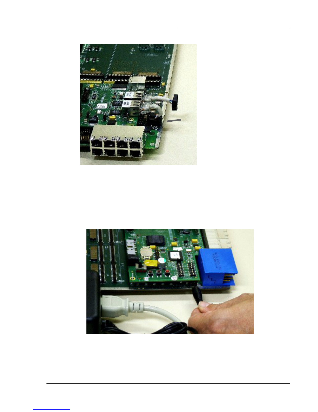
6. If you will be working with a back plane, and wish GETH signals to traverse either the
back plane connection, or the front plane optical connection, connect the two GETH
sockets on the MPC8349E MDS Processor Board with sockets on the PIB board as shown
in Figure 2-8 and Figure 2-9.
Note that if you do not do this, you can still connect GETH cables directly to the Processor
board’s sockets, if they are accessible in your laboratory configuration.
Processor Board on PIB
GETH Sockets
GETH Interconnecting
Cables
Figure 2-8 Insert GETH interconnecting cables to GETH sockets on Processor board
20 MPC8349E MDS Processor Board User’s Manual Freescale Semiconductor
Page 21
Hardware Preparation and Installation
GETH Interconnecting
Cable connected
Figure 2-9 Connect GETH interconnecting cables to sockets on PIB
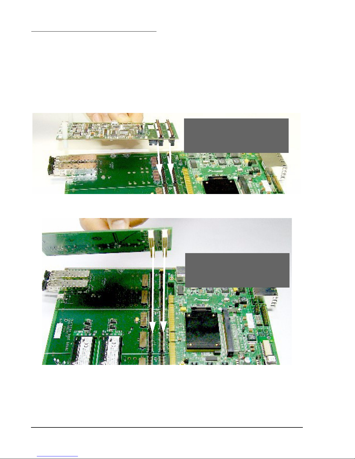
7. If you are not working with either the USB or the PCI cards, and you will be working with
the PIB in a “table-top” configuration (as opposed to inserting it in a rack to use its back
plane connections), you can at this point connect the power supply to the voltage input as
shown in Figure 2-10.
Power
Figure 2-10 Connecting Power input to the PIB
Freescale Semiconductor MPC8349E MDS Processor Board User’s Manual 21
Page 22
Hardware Preparation and Installation
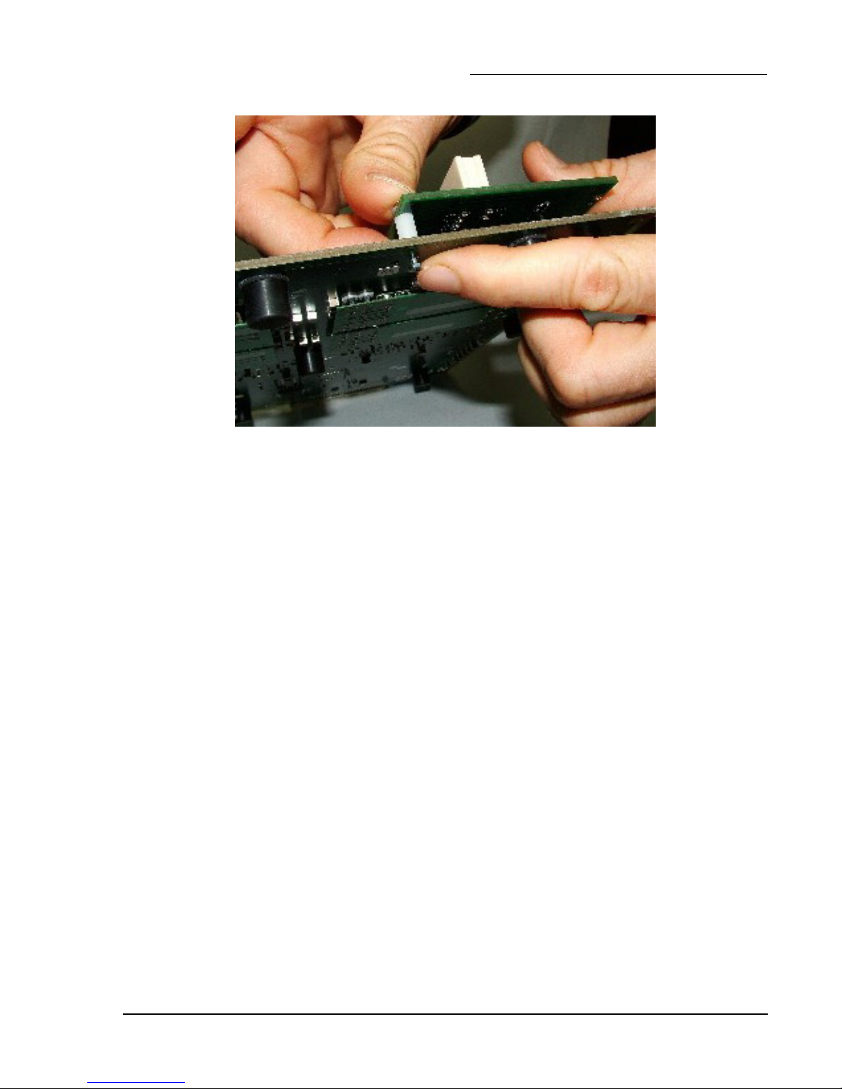
8. If you wish to work with the USB card, or any of the PCI cards, follow the illustrations in
Figure 2-11, Figure 2-12, and Figure 2-13 to connect these cards to the PIB.
Note that the USB card can only be inserted in the upper-most section, as shown. The PCI
card can be inserted in any section, for up to 4 PCI cards (up to 3 if using also a USB
card).
Connect using USB card’s
latches as shown
Tighten by hand
Figure 2-11 Connecting USB card to PIB
Connect using PCI card’s
latches as shown
Tighten by hand
Figure 2-12 Connecting PCI card to PIB
22 MPC8349E MDS Processor Board User’s Manual Freescale Semiconductor
Page 23
Hardware Preparation and Installation
Figure 2-13 Inserting spacers between PCI card and PIB
Freescale Semiconductor MPC8349E MDS Processor Board User’s Manual 23
Page 24
Hardware Preparation and Installation
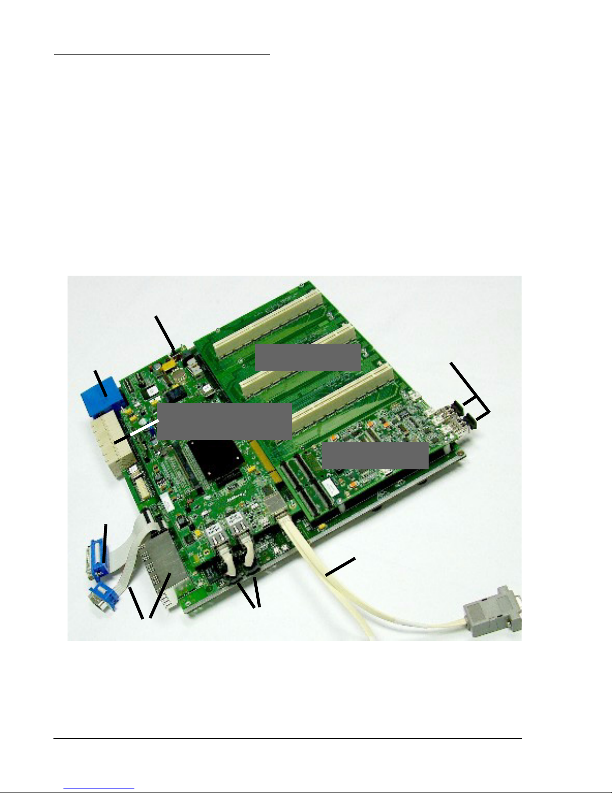
9. The fully assembled PIB-Processor board is shown in Figure 2-14, which also shows the
PIB external connections relevant when the MPC8349 is used.
All external connections of the Processor board are active when the Processor board is
installed on the PIB, except the voltage input (recieves power from the PIB power input,
or the back plane only), and the JTAG/COP connection (P9), which is replaced by the
parallel port connection to a PC.
Three PCI cards and one USB card are shown installed on the PIB. The PCI cards are
ready to receive any 83xx Processor board, installed in this case in the same manner as
they are in a PC. Using this system, these processor boards (up to three) function as slaves,
while the Processor board already installed functions as a master. This allows you to take
advantage of the parallel processing capabilities of the 83xx line of products.
.
Power input for “table-
top” configuration
Power input for
working with
a back plane
Back plane connection
(incl GETH and voltage)
Parallel port
to PC
Not relevant for MPC8349
PCI cards installed
GETH twisted pair
Front plane connection
(optical GETH)
USB card installed
Double RS-232
connected to RJ45 DUART
Figure 2-14 Fully Assembled Combined system:
PIB, Processor Board, USB, and PCI cards
24 MPC8349E MDS Processor Board User’s Manual Freescale Semiconductor
Page 25

Hardware Preparation and Installation
2.2.3 For Agent Mode only :
1. Insert the MPC8349E MDS Processor Board into a PC, using its PCI edge connector.
2. Operate Code Warrior® to verify that the processor board has been installed properly.
3. Connect external cables in accordance with your laboratory environment.
4. Verify that LD1 and LD2 turn on and then turn off (see Figure 2-3 for location). They
should be on for only a few moments. This indicates that the board has successfully
undergone the boot-up sequence.
Freescale Semiconductor MPC8349E MDS Processor Board User’s Manual 25
Page 26

Hardware Preparation and Installation
26 MPC8349E MDS Processor Board User’s Manual Freescale Semiconductor
Page 27

Memory Map
3
Memory Map
3.1 MPC8349E MDS Processor Board Mapping
The MPC8349 Memory Controller governs all accesses to the processor memory slaves.
Consequently, the memory map may be reprogrammed according to user needs. After performing
a Hard Reset, the debug host may initialize the memory controller via the JTAG/COP connector
in order to allow additional access to bus addressable peripherals. The DDR,SDRAM and
FLASH/PSRAM (optional) memories respond to all types of memory access - program/data and
Direct Memory Access (DMA).
.
Window
Number
7
5 80000000 -
6 A0000000 -
- C0000000 -
0 E0000000 -
Address Range Target Device Name
00000000 -
0FFFFFFF
(00000000 -
3FFFFFFF)
10000000 -
1FFFFFFF
(40000000 -
7FFFFFFF)
9FFFFFFF
BFFFFFFF
DFFFFFFF
E00FFFFF
Table 3-1. MPC8349SYS Memory Map
DDR SDRAM
HYMD232M646D
6
w/o ECC
MT9VDDT3272P
HG with ECC
PCI1 Inbound/Outbound win-
PCI2/Empty
Empty Space - 512MB -
8349 Internal Memory Regis-
a
Main SODIMM
CS2,CS3
Second SODIMM
(optional)
CS0,CS1
dow
Inbound/Outbound win-
dow
ter Space
Volume
in
Bytes
256MB
(1GB) 64+8
256MB
(1GB)
512MB 32/64
512MB 32
1MB 32
Port
Size in
Bits
ECC
- E0100000 EFFFFFFF
Freescale Semiconductor MPC8349E MDS Processor Board User’s Manual 27
Empty Space - ~256MB -
Page 28

Memory Map
Table 3-1. MPC8349SYS Memory Map
Window
Number
3 F0000000 -
- F5000000 -
- F8000000 -
- F8008000 -
- FE800000 - FFFFFFFF Empty Space - 24MB -
Address Range Target Device Name
F2FFFFFF
(F0000000 -
F4FFFFFF)
F7FFFFFF
F8007FFF
FDFFFFFF
FE000000 - FE7FFFFF
or
FE000000 - FE3FFFFF
Local Bus
SDRAM(optional)
on CS2
Empty Space - 64MB -
BCSR on CS1 Xilinx FPGA 32KB 8
Empty Space - ~96MB -
FLASH on CS0
or
PSRAM on CS0
(optional)
MT48LC16M16A2TG-
6A x 2
MT48LC16M16A2TG-
6A x 1
for parity
(MT48LC32M16A2TG-
7E)
MT28F640
TC51WHM516AXBN70
Volume
in
Bytes
64MB
(128MB)
8MB
4MB
Port
Size in
Bits
32+8
parity
16
a.PCI2 Memory Space defined for PCI2 host mode
The memory map defined in Table 3-1. "MPC8349SYS Memory Map" is only a recommendation.
The user can choose to work with alternative memory mapping. It should be noted that the
described mode is supported by Metrowerks’ Code Warrior® debug tool.
28 MPC8349E MDS Processor Board User’s Manual Freescale Semiconductor
Page 29
Controls and Indicators
Controls and Indicators
This chapter describes controls and indicators of the MPC8349E MDS Processor Board. This
includes switches, jumpers, LEDs, and other miscellaneous controls and indicators.
4.1 Switches and Jumpers Locations
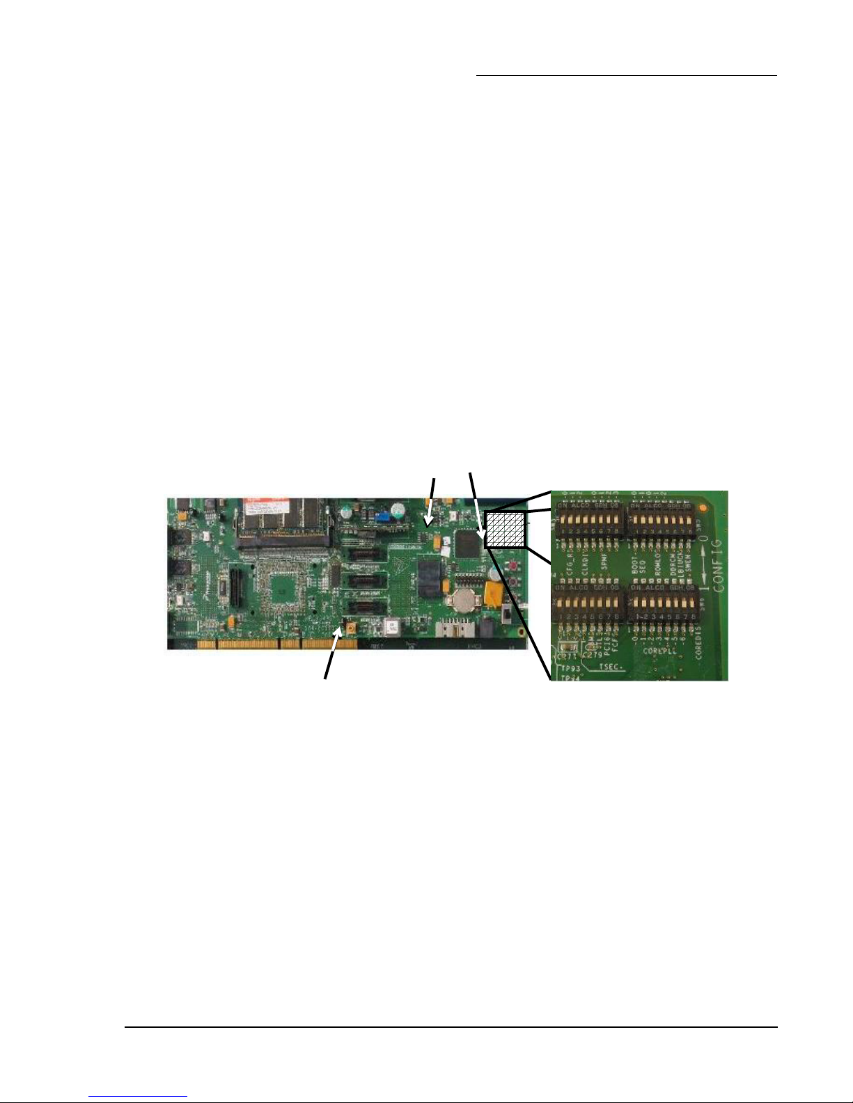
Figure 4-1 below shows the locations of the Jumpers and DIP Switches. Note that when “ON”,
the value of the switch is zero.
4
JP3
JP2
JP1
Figure 4-1 MPC8349E MDS Processor Board Switches and Jumpers Locations
DIP Switches
Freescale Semiconductor MPC8349E MDS Processor Board User’s Manual 29
Page 30

Controls and Indicators
4.1.1 Switches
The setting of DIP Switches are described in the publication HW Getting Started Guide for the
MPC8349E MDS Processor Board.
4.1.2 Jumpers
MPC8349E MDS Processor Board jumpers are described in the publication HW Getting Started
Guide for the MPC8349E MDS Processor Board.
4.2 LEDs
The MPC8349E MDS Processor Board has the following LEDs:
4.2.1 LD1, LD2 - Signaling LEDs
LED’s, LD1 (green) and LD2 (red), are program controlled. They are used for extra visibility on
the running utility. They are lit up by setting bits BCSR0.5-6 respectively.
4.2.2 LD3 - USB Power
When lit, the USB Vbus is powered.
4.2.3 LD4, LD5 - GETH Enable
The green LED, LD4,5, indicates enable for GETH Transceivers U5,U6.
4.2.4 LD6 - DUART Enable
A green LED, LD6, indicates enable for the RS232 Dual Transceiver.
4.2.5 LD7 - FUNC Indication
A green LED, LD7, indicates different board setting modes. LD7 blinks when the JTAG
controller, implemented in Xilinx FPGA, is active.
4.2.6 LD8 - Power GOOD
A green LED, LD8, indicates that the MPC8349E MDS Processor Board power is operating
normally.
4.2.7 LD9 - GPIO1-1 Indication
A green LED, LD9, indicates the state of the MPC8349 GPIO1-1 pin (U54/E24).
4.2.8 LD10, LD11 - PCTL0,1 USB
LED’s LD10, LD11 (green) are used for extra visibility on the USB Port 1.
4.2.9 LD12 - BOOT Indicator
The LD12 indicates MPC8349 boot processing.
30 MPC8349E MDS Processor Board User’s Manual Freescale Semiconductor
Page 31
Controls and Indicators
4.2.10 LD13 - 5V Power Indicator
The green LED, LD13, indicates a 5V power level on the MPC8349E MDS Processor Board.
A 5V power supply is plugged into the P11 Power Connector on the board’s front side for the
Stand-Alone Mode. The MPC8349E MDS Processor Board is powered by the 5V external power
supply when the SW5 Power Switch is turned to the “ON” (up) position.
When the MPC8349E MDS Processor Board is plugged into an PC via the PCI edge connector it
is powered from the edge connector’s 5V power rail (Agent Mode). In the PIB Combined Mode,
5V power is supplied from the PIB’s power supply via risers connectors. Note that if working in
either of these two modes, the position of SW1 is ignored.
4.3 Other Controls and Indicators
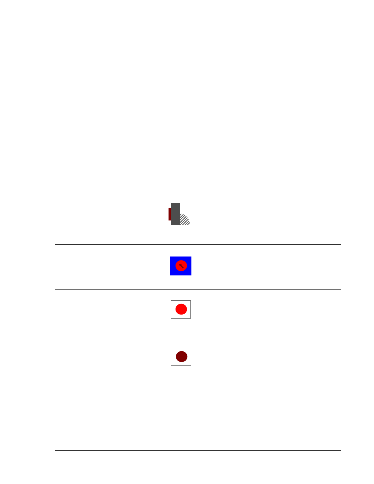
Table 4-1. The MPC8349E MDS Processor Board Push Buttons
Pressing button SW1 results in Power-OnReset for all components on the MPC8349E
SW1
Power-on-Reset
PRESET
MDS Processor Board.
Use this reset button when the MPC8349E
MDS Processor Board is installed in a PC.
SW2
Software Option
SW8
Slave Hard Reset
SW9
Soft Reset
SW OPT
HRESET
SRESET
Rotary Switch SW2 allows the user to change
the program flow according to eight available
cases.
Not available when installed in a PC.
Pressing button SW8 results in a Hard Reset
for the MPC8349E.
Not available when installed in a PC.
Pressing button SW9 results in a Soft Reset for
the MPC8349E. Despite the reset, clock and
chip-select data as well as SDRAM (if installed)
contents are retained.
Not available when installed in a PC.
Freescale Semiconductor MPC8349E MDS Processor Board User’s Manual 31
Page 32
Controls and Indicators
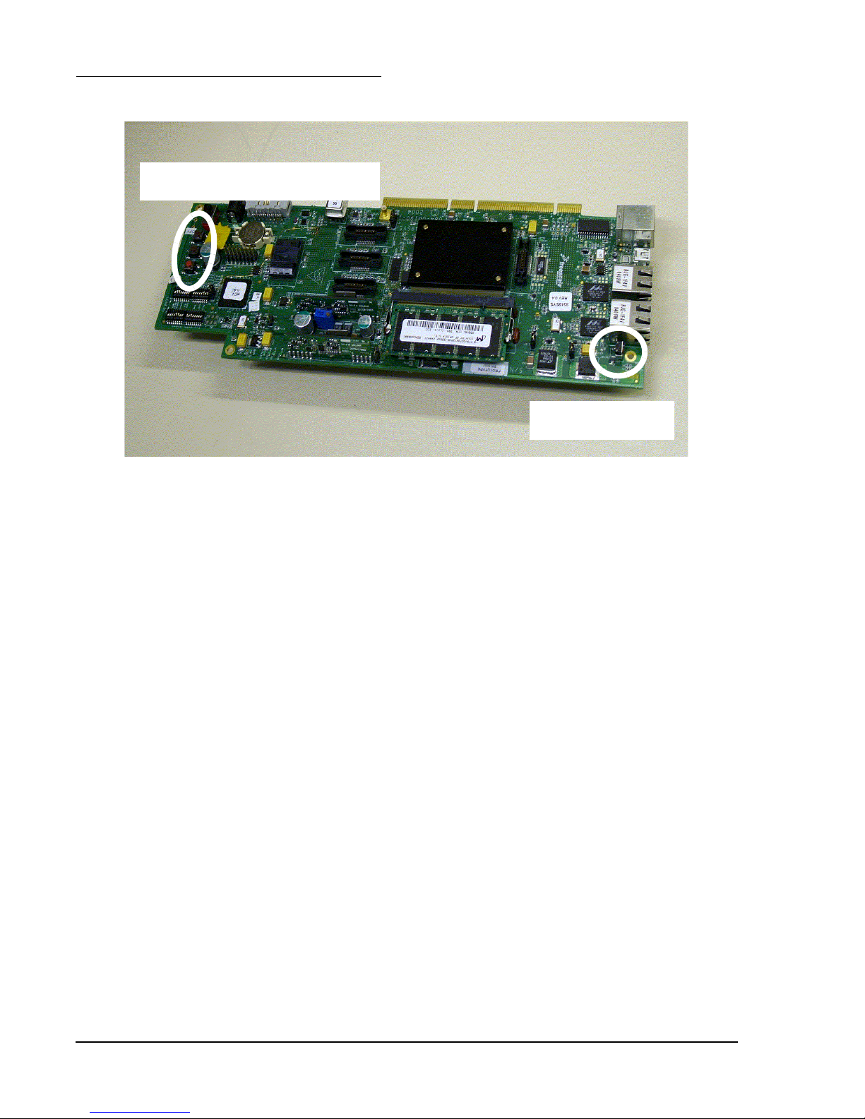
SW7, 8, 9, 10: Resets and NMI
SW1: Aux. POR
Figure 4-2 MPC8349E MDS Processor Board Push Buttons and Auxiliary POR
32 MPC8349E MDS Processor Board User’s Manual Freescale Semiconductor
Page 33

Functional Description
5
Functional Description
In this chapter the design details of various modules of the MPC8349E MDS Processor Board are
described. This includes memory map details and software initialization of the board.
5.1 Reset & Reset - Configuration
There are several reset sources on the MPC8349E MDS Processor Board:
• Power On Reset
• Manual Hard-Reset
• Manual Soft-Reset
• MPC8349 (see also the MPC8349 U/M)
5.1.1 Power - On Reset
The power on reset to the MPC8349E MDS Processor Board initializes the processor’s state after
power up. A dedicated logic unit asserts PORESET input for a period long enough to cover the
MPC8349 core voltage stabilization. When the MPC8349E MDS Processor Board is working in
Stand-Alone Mode or PIB Combined Mode, a Power-On-Reset may be generated manually as
well by an on-board dedicated push-button (SW1).
In addition, a power on reset for the MPC8349 can be done by toggling bit #7 in BCSR7.
5.1.2 Hard Reset
Hard-Reset may be generated on the MPC8349E MDS Processor Board by any one of the
following sources:
• COP/JTAG Port (in Stand-Alone Mode only)
• Manual Hard reset.
• Internal sources.
Hard-Reset, when generated, causes the MPC8349 to reset all its internal hardware except for
PLL logic and re-acquires the Hard-reset configuration from its current source. Since hard-reset
also resets the refresh logic for dynamic RAMs, their content is lost as well.
CAUTION
Freescale Semiconductor MPC8349E MDS Processor Board User’s Manual 33
HRESET is an open-drain signal and must be
driven with an open-drain gate by whatever
external source is driving it. Otherwise,
Page 34

Functional Description
contention will occur over that line, and that
might cause permanent damage to either board
logic and/or to the MPC8349.
5.1.2.1 COP/JTAG Port Hard - Reset (stand-alone only)
To provide convenient hard-reset capability for a COP/JTAG controller, an HRESET line has
been connected to the COP/JTAG port connector. The COP/JTAG controller may directly
generate a hard-reset by asserting (low) this line.
5.1.2.2 Manual Hard Reset
To allow a run-time Hard-reset, a manual Hard-reset is facilitated, via SW8. Note that this cannot
be done when the MPC8349E MDS Processor Board is connected in a PC (Agent Mode), but
instead SW1 can be used.
In addition, a manual hard reset for the MPC8349 can be done by toggling bit #4 in the CCR
register.
5.1.2.3 Manual Soft Reset
To allow a run-time Soft-reset, manual Soft-reset is facilitated, via SW9. Note that this cannot be
done when the MPC8349E MDS Processor Board is connected in a PC (Agent Mode).
In addition, a manual hard reset for the MPC8349 can be done by toggling bit #5 in the CCR
register.
5.2 Board Control & Status Registers – BCSR
The BCSR is an 8-bit wide read / write register file that controls or monitors most of the
MPC8349E MDS Processor Board hardware options. The BCSR’s register may be accessed from
the Local Bus or via the FPGA internal JTAG controller. The BCSR includes up to 16 registers,
some of which are optional.
BCSR registers are duplicated numerous times within a CS1 region. This is due to the CS region’s
32KB minimum block size and the fact that only address lines A[28:31] are decoded for register
selection by the BCSR. BCSR is implemented on a Xilinx FPGA device that provides register and
logic functions over some MPC8349E MDS Processor Board signals.
The BCSR controls or monitors the following functions:
1. Power-on-Reset & Hardware configuration setting for the processor.
2. Most of the Hardware Reset Configuration bits are stored in BCSR registers available
from the Local Bus or JTAG.
3. Hard- Soft- Reset and NMI (IRQ) pushbuttons debounce function.
4. Hardware Configuration for the both GETH transceivers.
5. Enable/Disable to:
- Two GETH1,2 Transceivers.
34 MPC8349E MDS Processor Board User’s Manual Freescale Semiconductor
Page 35

Functional Description
- Dual RS232 Transceiver.
- PSRAM (if installed) or FLASH select.
- SHMOO function.
- LED off.
6. BCSR provides h/w write protection for FLASH and BRD I2C EEPROM .
7. Two LEDs (one green, one red) provide s/w signaling.
8. Special CCR - COP register for JTAG port connectivity.
9. Status registers BCSR10, BCSR11 include:
- PCI Host Mode indicates if the Board is working in a Host Mode (Stand-Alone or PIB
Combined) or the Agent Mode
- Processor Low Power Mode (QUISCE)
- Software Option Identification (set by SW2 Rotary Switch)
- BCSR Revision code
Sections of the BCSR slice control registers generally have low active notations. This means that
a bit function will be realized while the bit is zero. When a bit is set to high a related function is
disabled. The default setting is assumed to be non-functional. The most significant bit is bit 0.
5.2.1 BCSR0 - Board Control / Status Register 0
The BCSR0 serves as a 8-bit control register on the board The BCSR0 may be read or written at
any time. BCSR0 defaults are attributed immediately after a Power-On Reset or HRESET.
BCSR0 fields are described below in Table 5-1.:
Table 5-1. BCSR0 Description (Offset 0)
Default
BIT MNEMONIC Function
0 GETH1EN GETH Transceiver 1 Enable. Upon activation (low), the
MPC8349 TSEC port 1 transceiver is enabled. When negated
(high), the GETH Transceiver enters standby mode. May be
rewritten via JTAG/LBIU.
1 GETH2EN GETH Transceiver 2 Enable. Upon activation (low), the
MPC8349 TSEC port 1 transceiver is enabled. When negated
(high), the GETH Transceiver enters standby mode. May be
rewritten via JTAG/LBIU.
2 GETHRST GETH Transceiver Reset. The GETH devices are reset when
the GETHRST is asserted (low). The Board Hard Reset signal
of the MPC8349 resets GETH devices. May be rewritten via
JTAG/LBIU.
upon
HRST
0R,W
0R,W
1R,W
Attr.
3 RS232EN UART Ports Transceivers Enable. Upon activation (low), the
Dual RS232 Transceiver, using the UART ports of the
MPC8349, is enabled. When negated (high), the RS232
Transceiver enters standby mode. May be rewritten via JTAG/
LBIU.
Freescale Semiconductor MPC8349E MDS Processor Board User’s Manual 35
0R,W
Page 36

Functional Description
Table 5-1. BCSR0 Description (Offset 0)
BIT MNEMONIC Function
Default
upon
HRST
Attr.
4 BOOTWP BOOT I2C EEPROM Protect. When asserted (low) BOOT
EEPROM functions normally, when negated (high) write
operations are disabled. May be rewritten via JTAG/LBIU.
5 SIGNAL0 Signal LED 0. A dedicated Green LED is illuminated when
SIGNAL0 is active (low). The LED is unlit when it is in an
inactive (default) state (high). During the Reset Configuration
sequence the LED indicates the SRESET assertion. The user
may utilize the LED for software Slave signalling purposes.
May be rewritten via JTAG/LBIU.
6 SIGNAL1 Signal LED Slave 1. A dedicated Red LED is illuminated when
SIGNAL1 is active (low). The LED is unlit when it is in an
inactive (default) state (high). During the Reset Configuration
sequence the LED indicates the HRESET assertion. May be
rewritten via JTAG/LBIU.
7 SPARE07 Not Implemented. 1 R,W
1R,W
1R,W
1R,W
5.2.2 BCSR1 - Board Control / Status Register 1
On the board, the BCSR1 acts as a control register. The BCSR1, which may be read or written at
any time, receives its defaults immediately after Power-On or PORESET. The BCSR1 fields are
described below in Table 5-2.:
Table 5-2. BCSR1 Description (Offset 1)
BIT MNEMONIC Function Defn. Attr.
0 CFG_CLKIN_DIVCLKIN Division. The bit reflects CFG_CLKIN_DIV signal
logic level during Power Reset Configuration sequence.
The bit is set by default by appropriate DIP switch SW3.4.
May be rewritten via JTAG/LBIU.
1-3 CFG_RS[0:2] Reset Configuration Words Source. The bits reflect
CFG _RS[0:2] signals logic level during PON Reset
Configuration sequence. The bits are set by default by
appropriate DIP switch SW3.1-3. May be rewritten via
JTAG/LBIU.
4-6 ROMLOC[0:2] Boot ROM interface location. The bits reflect
ROMLOC[0:2] signals logic level during Reset
Configuration sequence. The bits are set by default by
appropriate DIP switch SW6.3-5. May be rewritten via
JTAG/LBIU.
SW3.4
Sampled
at Power
ON
SW3.1-3
Sampled
at Power
ON
SW5.3-5
Sampled
at
PORESET
neg.
R,W
R,W
R,W
36 MPC8349E MDS Processor Board User’s Manual Freescale Semiconductor
Page 37

Functional Description
Table 5-2. BCSR1 Description (Offset 1)
BIT MNEMONIC Function Defn. Attr.
7 FLASHPRT Flash Protect. Upon activation (low) the Flash may be
written. When high the write protection is set.
1
Sampled
at
PORESET
neg.
5.2.3 BCSR2 - Board Control / Status Register 2
On the board, the BCSR2 acts as a control register. The BCSR2, which may be read or written at
any time, receives its defaults immediately after the PORESET signal. The BCSR2 fields are
described below in Table 5-3.:
Table 5-3. BCSR2 Register Description (Offset 2)
Default
BIT MNEMONIC Function
0-3 SPMF[0:3] System PLL Multiplication Factor. The four bits reflect
SPMF[0:3] signals logic level during Hard Reset Configuration
sequence. The bits are set by default by appropriate DIP
switch SW3.5-8. May be rewritten via JTAG/LBIU.
upon
PORESET
SW3.5-8 R,W
R,W
Attr.
4-5 SVCOD[4:5] VCO Division. The two bits reflect SVCOD[4:5] signals logic
level during Hard Reset Configuration sequence. The bits are
set low by default. May be rewritten via JTAG/LBIU.
6-7 BOOTSEQ[6:7] Boot Sequencer Configuration. The two bits reflect
BOOTSEQ[6:7] signals logic level during Reset Configuration
sequence. The bits are set by appropriate DIP switch SW5.1-
2. May be rewritten via JTAG/LBIU.
0R,W
SW5.1-2 R,W
5.2.4 BCSR3 - Board Control / Status Register 3
On the board, the BCSR3 acts as a control register. The BCSR3, which may be read or written at
any time, receives its defaults immediately after the PORESET signal. The BCSR3 fields are
described below in Table 5-4.:
Freescale Semiconductor MPC8349E MDS Processor Board User’s Manual 37
Page 38

Functional Description
.
Table 5-4. BCSR3 Register Description (Offset 3)
BIT MNEMONIC Function
Default
upon
PORESET
Attr.
0-6 COREPLL[0:6] Core PLL Multiplication Factor. The seven bits reflect
COREPLL[0:6] signals logic level during Hard Reset
Configuration sequence. The bits are set by default by
appropriate DIP switch SW7.1-7. May be rewritten via
JTAG/LBIU.
7 SWEN Software Watchdog Enable. The bit reflect SWEN signals
logic level during Hard Reset Configuration sequence. The
bit are set by default by appropriate DIP switch SW6.8.
May be rewritten via JTAG/LBIU.
SW7.1-7 R,W
SW6.8 R,W
5.2.5 BCSR4 - Board Control / Status Register 4
On the board, the BCSR4 acts as a control register. The BCSR4, which may be read or written at
any time, receives its defaults immediately after PORESET signal. The BCSR4 fields are
described below in Table 5-5.:
Table 5-5. BCSR4 Description (Offset 4)
Default
BIT MNEMONIC Function
0PCIHOST PCI Host Mode. If working as a PCI add-in card (Agent
Mode), this bit is set low. When the MPC8349E MDS
Processor Board is combined with the PIB (PIB combined
mode), the PCIHOST bit will be high to set PCI
processor’s port as the host mode. May be rewritten via
JTAG.
upon
PORESET
Defined by
operating
configuration
Attr.
R,W
1 PCI64 PCI 64-bit Mode. The bit reflects PCI64 signal logic level
during Hard Reset Configuration sequence. When it is low
the PCI1,2 ports are 32-bit mode, if high the PCI1 port
uses 64-bit I/F. The bit is controlled by the appropriate DIP
switch SW4.7. May be rewritten via JTAG/LBIU.
2 PCI1ARB PCI1 Arbiter. If working in Agent Mode, this bit is set low to
provide external arbiter When the MPC8349E MDS
Processor Board is working in the PIB Combined Mode,
this bit is set high to configure the PCI1 port with an
internal arbiter. May be rewritten any time via JTAG.
38 MPC8349E MDS Processor Board User’s Manual Freescale Semiconductor
SW4.7 DIP
Switch
Defined by
operating
configuration
R,W
R,W
Page 39

Table 5-5. BCSR4 Description (Offset 4)
BIT MNEMONIC Function
Functional Description
Default
upon
Attr.
PORESET
3 PCI2ARB PCI2 Arbiter. If working in the Agent Mode, this bit is set
low to provide an external arbiter. When the MPC8349E
MDS Processor Board is working in the PIB Combined
Mode, this bit is set high to configure the PCI2 port with an
internal arbiter. May be rewritten any time via JTAG.
4 COREDIS Core Disable. When high the e300 core is prevented from
fetching boot code until configuration by an external master
is complete. If low, the core runs normally. May be
rewritten any time via JTAG.
5 BMS Boot Mode. When low, sets lower 8MByte boot memory
space location if used for DDR or PCI boot source.
Otherwise (for LBIU boot source), the BMS will be high for
upper boot memory space location. User may change boot
source location by request. May be rewritten any time via
JTAG/LBIU.
6 LBIUCM Local Bus Clock Mode. When set high local bus memory
controller operates with a frequency equal to twice the
frequency of the csb_clk. If this bit is low, the local bus
memory controller will operate at the csb_clk frequency.
The DIP-switch SW6.7 may change LBIUCM bit setting.
May be rewritten any time via JTAG/LBIU.
7 DDRCM DDR SDRAM Clock Mode. If this bit set high, the DDR
SDRAM memory controller operates with frequency equal
to twice the frequency of the csb_clk. If this bit is low, the
DDR SDRAM memory controller operates at the csb_clk
frequency. The DIP-switch SW6.6 may change DDRCM bit
setting. May be rewritten any time via JTAG/LBIU.
Defined by
operating
configuration
Setup
defined
SW4.5 R,W
SW6.7 R,W
SW6.6 R,W
R,W
R,W
Freescale Semiconductor MPC8349E MDS Processor Board User’s Manual 39
Page 40

Functional Description
5.2.6 BCSR5 - Board Control / Status Register 5
On the board, the BCSR5 acts as a control register. The BCSR5, which may be read or written at
any time, receives its defaults immediately after the PORESET signal. The BCSR5 fields are
described below in Table 5-6.:
Table 5-6. BCSR5 Description (Offset 5)
Default
BIT MNEMONIC Function
upon
PORESET
Attr.
0-1 TSEC1M TSEC port 1 Config Mode. Two bits select standard/
reduced versus width and the protocol used by the TSEC1
controller. See Table 5-7. May be rewritten any time via
JTAG/LBIU.
2-3 TSEC2M TSEC port 2 Config Mode. Two bits select standard/
reduced versus width and the protocol used by the TSEC2
controller. See Table 5-7. May be rewritten any time via
JTAG/LBIU.
4 TSEC1MST GETH1 Master Mode. If high GETH1 transceiver
configures in Master Mode. Otherwise when low GETH1
transceiver operates as Slave. May be rewritten any time
via JTAG/LBIU.
5 TSEC2MST GETH2 Master Mode. If high GETH2 transceiver
configures in Master Mode. Otherwise when low GETH2
transceiver operates as Slave. May be rewritten any time
via JTAG/LBIU.
6 INT_USB Internal USB phy. If high on-board USB phy is tied to USB
port 0 MPC8349. When working in the PIB Combined
Mode, the INT_USB bit initiates low to select off-board
USB phys and disable on-board USB phy. Wrong
programming in PIB Combined Mode may cause USB
digital signals contention.
SW4.1-2 R,W
SW4.3-4 R,W
1R,W
1R,W
0 - for
combined
mode;
1 - for other
modes
R,W
7 SPARE5 Not Implemented. 11 -
Setting Value TSEC Mode
00 The TSEC controller operates in the RGMII protocol, using only four transmit
data signals and four receive data signals.
01 The TSEC controller operates in the RTBI protocol, using only four transmit
data signals and four receive data signals.
10 The TSEC controller operates in the GMII protocol, using eight transmit data
signals and eight receive data signals.
40 MPC8349E MDS Processor Board User’s Manual Freescale Semiconductor
Table 5-7. TSEC Port Mode
Page 41

Functional Description
Setting Value TSEC Mode
11 The TSEC controller operates in the TBI protocol, using eight transmit data
signals and eight receive data signals.
5.2.7 BCSR6 - Board Misc. Register 1
On the board, the BCSR6 acts as a control register. The BCSR6, which may be read or written at
any time, receives its defaults immediately after PORESET signal. The BCSR6 fields are
described below in Table 5-8..
Table 5-8. BCSR6 Description (Offset 6)
Default
BIT MNEMONIC Function
upon
PORESET
Attr.
0 SPARE60 Not implemented. N/A R,W
1 TPR Test Port Enable. Should be set high to place the
processor in Test Mode. When low the processor
operates in normal mode. May be rewritten any time via
JTAG.
2 TLE True Little Endian. Low selects Big Endian Mode. High
value provides Little Endian Mode. May be rewritten any
time via JTAG.
3 LALE Local Bus Timing. When bit sets high LALE has earlier
negation. Low provides normal LALE timing. May be
rewritten any time via JTAG.
4 JTAG2SEL JTAG Chain Select. Select JTAG chain for external
devices on PMC cards when high. Low provides JTAG
normal configuration.
5-7 SPARE65-7 Not Implemented. ‘111’ -
0R,W
0R,W
0R,W
0R
5.2.8 BCSR7 - Board Misc. Register 2
On the board, the BCSR7 acts as a control register. The BCSR7, which may be read or written at
any time, receives its defaults immediately after PORESET signals. The BCSR7 fields are
described below in Table 5-9..
Freescale Semiconductor MPC8349E MDS Processor Board User’s Manual 41
Page 42

Functional Description
Table 5-9. BCSR7 Description (Offset 7)
BIT MNEMONIC Function
Default
upon
PORESET
Attr.
0 TESTEN Enable Chip Test Mode. For Internal use only. May be
rewritten any time via JTAG.
1 LEDEN LEDs Enable. All LEDs remain darkened for Failure
Analysis purposes when set high. When low, the LEDs
behave normally according to Section 4.2 "LEDs". May be
rewritten any time via JTAG/LBIU.
2 SHMOOEN SHMOO Test Enable. An enable signal to allow
programming of the Internal Core Power Supply and the
application of an external clock from the PIB Board when
low. May be rewritten any time via JTAG./LBIU.
3 EM FLASH Emulation (PSRAM). Low enables PSRAM
accesses to provide Flash emulation. When high PSRAM
is disabled, Flash may be enabled instead. May be
rewritten any time via JTAG/LBIU.
4 FLEN FLASH Enable. Low enables Flash accesses. When
high Flash operation is not available, PSRAM part may
be enabled instead. May be rewritten any time via JTAG/
LBIU.
5 BUFFEN Expansion Buffer Enable. Low enables access to the PIB
for the PIB combined mode. High level sets off the
expansion buffer for the stand alone mode. May be
rewritten any time via JTAG/LBIU.
0R,W
0R,W
1
Set at
Power On
1R,W
0R,W
Setup
defined at
Power On
R,W
R,W
6 BRDWP BRD Write Protect. When high the BRD EEPROMs on
the MPC8349E MDS Processor Board are hardware
protected for write operation. Low level allows the content
of the BRDs to be updated. May be rewritten any time via
JTAG/LBIU.
7 PORESET Power-On-Reset. Toggling low-high within 1ms time
window will generate a PORESET negative pulse on the
MPC8349E MDS Processor Board. May be rewritten any
time via JTAG/LBIU.
1
Set at HRST
1R,W
R,W
5.2.9 BCSR8 - Board Misc. Register 3
On the board, the BCSR8 acts as a control register. The BCSR8, which may be read or written at
any time, receives its defaults immediately after PORESET. The BCSR8 fields are described
below in Table 5-10.
42 MPC8349E MDS Processor Board User’s Manual Freescale Semiconductor
Page 43

Functional Description
Table 5-10. BCSR8 Description (Offset 8)
BIT MNEMONIC Function Defn. Attr.
0 CNFLOCK Config Bit Lock. When low BCSR contents don't update
during PORESET. High provides normal operation when
BCSR default value is set according DIP switches. Used
for debug purpose. May be rewritten any time via JTAG.
1-7 SPARE8 Not Implemented. ‘1111111’ R,W
1
Set at
Power
On
R,W
5.2.10 BCSR10 - Board Status Register 1
The BCSR10 is a read-only status register. The BCSR10 fields are described below in Table 5-11..
Table 5-11. BCSR10 Description (Offset 0xA)
BIT MNEMONIC Function
0 PCI_HOST PCI_HOST. Indicates the board’s working mode. This is
high when installed in a PC (Agent Mode), and low when
in Stand-Alone or PIB Combined Mode.
1 QUISCE QUISCE Status. Allows the processor to determine the
power down mode when bit is low by reading via JTAG. If
the bit is high, the power down mode is determined by
internal processor logic, regardless of JTAG settings.
2-4 SWOP Software Option Three-bit code reading from the SW2
switch.
5 FCFG FLASH Configuration. When high and configuration
source set as Local Bus (BCSR1.1-3 = 0) the RCW is
loaded from FLASH, if low, the RCW is loaded from the
BCSR.
6-7 - Not Implemented.
5.2.11 BCSR11 - Board Status Register 2
The BCSR11 Register is a status register accessed from the Local Bus. The BCSR11 fields are
described below in Table 5-12..
Freescale Semiconductor MPC8349E MDS Processor Board User’s Manual 43
Page 44

Functional Description
Table 5-12. BCSR11 Description (Offset 0xB)
BIT MNEMONIC Function Attr.
0-3 REV BCSR Revision. Four most significant bits revision coding Programmed
value
4-7 SubREV BCSR Revision. Four least significant bits revision coding Programmed
value
Table 5-13. BCSR Revision Coding
Revision Number
[0:3]
0.x
1.x RevA
Board Revision
Proto
Pilot
5.2.12 CCR - COP Control Register
CCR - COP Control Register is a service register accessed from the Local Bus. It is a part of
PCI2JTAG converter for the Agent Mode (when the Processor Board is plugged into a PC). The
CCR fields are described below in Table 5-14.
Table 5-14. CCR Description (Offset 0xF)
Default
BIT MNEMONIC Function
T D I T A P D a t a I n p u t . D r i v e serial Data into COP port. Disabled W
0
T D O T A P D a t a O u t p u t . R e a d s erial Data from COP port. Disabled R
upon
PORESET
Attr.
1 TCK TAP Clock. When asserted (low), TAP clock is enabled,
and driven into the COP port. If negated (high), TAP
clock is disabled.
2 TMS TAP Mode Select. Drive TMS signal into COP port. Disabled W
3 TRST TAP Reset. Reset TAP controller of COP port. Disabled W
4 HRESET Hard Reset. Low provides short negative HRST pulse on
the board.
44 MPC8349E MDS Processor Board User’s Manual Freescale Semiconductor
Disabled W
Disabled W
Page 45

Table 5-14. CCR Description (Offset 0xF)
BIT MNEMONIC Function
Functional Description
Default
upon
Attr.
PORESET
5 SRESET Soft Reset. Low provides short negative SRST pulse on
the board.
6 CKSTPI Check Stop. Causes Machine Check Stop of the
processor.
7 COPEN CCR COP Enable. Low permits access to processor
JTAG port via CCR register. High disables the CCR
register.
Disabled W
W
1W
5.3 External Connections
5.3.1 P1 - MiniAB USB Connector
MiniAB USB connector pinout is shown in Table 5-15. "P1-MiniAB USB Connector" below.
This connector is used for connectivity to external devices USB1.1/USB2.0/OTG. It is accessible
from the front panel of the board (see Figure 1-1 for location).
Table 5-15. P1-MiniAB USB Connector
Pin
No.
Signal Name Description
1 Vbus 5V Power for USB - Power is generated internally if working in PCI
mode or is supplied from a cable (in stand-alone mode) while the USB
controller configures the device
2 DM Differential Negative Data
3 DP Differential Positive Data
4 ID Identification Signal for Host/Device Mode Setting
(PCI mode vs. stand-alone mode)
5 GND Ground
5.3.2 P2 - DUART Port
The DUART port connector - P2 is implemented with a 90o, 10-pin, RJ45 connector, signals of
which are described in Table 5-16.
Freescale Semiconductor MPC8349E MDS Processor Board User’s Manual 45
Page 46

Functional Description
Table 5-16. P2 DUART Signals
Pin
No.
1CTS1
2RXD1 IReceive Data
3 TXD1 O Transmit Data
4 RTS1 O Ready To Send
5,10 GND P Ground.
6CTS2
7RXD2 IReceive Data
8 TXD2 O Transmit Data
9 RTS2 O Ready To Send
Signal
Name
UART
Port
1
2
Attr. Description
IClear To Send
IClear To Send
For connection to regular D-Type-9 RS232 cable use special cable from MPC8349E MDS
Processor Board set.
5.3.3 Logic Analyzer Connectors
P3, P6, P7, and P8 are 38-pin, SMT, high density, matched impedance connectors made by AMP
and used for Logic Analyzer measurements. They contain all MPC8349 signals, except for the
DDR signals.
5.3.4 P5 - SMB Connector
RF Subminiature Coaxial Connector P5 is used to connect an external clock to the MPC8349,
which is enabled only when jumper JP1/2-3 is closed. Optional.
5.3.5 P9 - Debug COP Connector
P9 is a Freescale-standard JTAG/COP connector for the PowerPC. It is a 16 pin 90o two row
header connector with key. During debug, all processors connected by the JTAG chain may be
accessed through connector P9. The pinout of P9 is shown in Table 5-17. "P9 - JTAG/COP
Connector" below:
Table 5-17. P9 - JTAG/COP Connector
Pin No. Signal Name Attr. Description
1 TDOc I Transmit Data Output. This is the MPC8349 JTAG serial
data output driven by Falling edge of TCK.
2,10,12,
16
GND P Main GND plane.
46 MPC8349E MDS Processor Board User’s Manual Freescale Semiconductor
Page 47

Functional Description
Table 5-17. P9 - JTAG/COP Connector
Pin No. Signal Name Attr. Description
3 TDIc O Transmit Data In. This is the JTAG serial data input of the
MSC8101, sampled on the rising edge of TCK.
4 nTRSTc O Test port Reset. When this signal is active (Low), it resets
the JTAG logic. This line is provides a pull-down on the
ADS with a 4.7KΩ resistor, which provides a continuous
reset of the JTAG logic, when connector is unplugged.
5 N.C. - Not Connected.
6 SENSE P Connect to 3.3V power supply bus via protection resistor.
May be used for Command Convertor power.
7 TCKc O Test port Clock. This clock shifts in / out data to / from the
JTAG logic. Data is driven on the falling edge of TCK and is
sampled both internally and externally on its rising edge.
8 Check Stop Input I Machine Check Stop Input
9 TMSc O Test Mode Select. This input selects test mode and is
sampled on the rising edge of TCK. This line is qualified
with TCK in a same manner as TDI, and changes the state
of the JTAG machines. This line is pulled up internally by
the MPC8349.
11 nSRSTc I/O,P.U. When asserted by an external H/W, generates Soft-Reset
sequence for the MPC8349. Pulled Up on the ADS using a
4.7KΩ resistor.
When driven by an external tool, MUST be driven with an
Open Drain gate. Failure to do so might result in
permanent damage to the processor and / or to ADS
logic.
13 nHRSTc I/O,P.U. When asserted by an external H/W, generates Hard-Reset
sequence for the MPC8349. Pulled Up on the ADS using a
4.7KΩ resistor.
When driven by an external tool, MUST be driven with an
Open Drain gate. Failure to do so might result in
permanent damage to the processor and / or to ADS
logic.
14 KEY - No pin in connector. Serves for correct plug insertion. See
Figure 5-1 for location.
15 Check Stop Output O Machine Check Stop Output
Freescale Semiconductor MPC8349E MDS Processor Board User’s Manual 47
Page 48

Functional Description
P9
14
115
216
Figure 5-1 P9 COP connector front view
5.3.6 P10 - FPGA’s In-System-Programming (ISP)
This is a 16 pin generic 0.100" pitch header connector, providing In System Programming
capability for on board programmable logic devices by Xilinx FPGA (Spartan-2E). The pinout of
P10 is shown in Table 5-18. "P10 - FPGA Programming ISP Connector" below:
Table 5-18. P10 - FPGA Programming ISP Connector
Pin No. Signal Name Attr. Description
1 ISP_TDO I Transmit Data Output.
2,10,12,
16
GND P Main GND plane.
3 ISP_TDI O Transmit Data In.
4,5,8,11,
13,14,15
6 SENSE P Connect to 3.3V power supply bus via pro-
7 ISP_TCK O Test port Clock.
9 ISP_TMS O Test Mode Select.
N.C. - Not Connected.
tection resistor. Use for programmer power-
ing.
5.3.7 P11 - Power Connector
P11 is 2mm Power Jack RAPC722 which provides a connection to an external power supply
[email protected].
48 MPC8349E MDS Processor Board User’s Manual Freescale Semiconductor
Page 49

Functional Description
5.3.8 J1,J2 - Ethernet Port Connector
The Ethernet connectors on the MPC8349 (J1,J2) are both Twisted-Pair (1000-Base-T)
compatible connectors. They are implemented with a 90o, 8-pin, RJ45 Combo connector with
internal magnetics and two LEDs (indicating communication speed), signals of which are
described in Table 5-19. "J1,J2 - Ethernet Port Interconnect Signals" below. These connections
are on the front panel. For location, see Table 1-1. Green LED indicates 1000Mbit Data rate,
Yellow LED is lit when 100Mbit Data rate mode. .
Table 5-19. J1,J2 - Ethernet Port Interconnect Signals
Pin
No.
1 White Twisted-Pair Transmit Data
2 White-Orange Twisted-Pair Transmit Data
3 White-Green Twisted-Pair Receive Data
4 Blue Unused BI-DC+
5 White-Blue Unused BI-DC-
6 Green Twisted-Pair Receive Data
7 White-Brown Unused BI-DD+
8 Brown Unused BI-DD-
Wire Color 10Base-T/100Base-T Signal 1000 Base-T Signal
BI-DA+
positive output
BI-DA-
negative output.
BI-DB+n
positive input.
BI-DB-
negative input
Freescale Semiconductor MPC8349E MDS Processor Board User’s Manual 49
Page 50

Functional Description
50 MPC8349E MDS Processor Board User’s Manual Freescale Semiconductor
Page 51
Clocking for the MPC8349E MDS Processor Board
6
Clocking for the MPC8349E MDS Processor
Board
This chapter describes the clocking and timing of the MPC8349 while being used on the
MPC8349E MDS Processor Board.
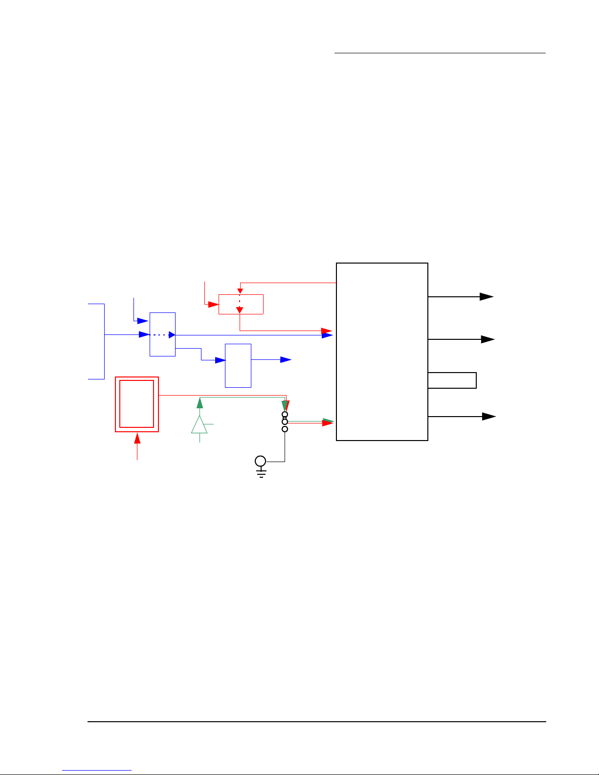
Two primary clock sources are available for the MPC8349: CLKIN or PCICLK, depending on
whether the device is a Host (that is, in Stand-Alone or PIB Combined Mode) or working in the
Agent Mode (inserted in a PC compatible computer).
Mode2
CLK
PCI Edge Con
U22
CLOCK
OSC
66 MHz
OE
Mode1
Mode1 - Host Modes
Mode2 - Agent Mode
Mode3 - SHMOO M
U1001
ZD
Buffer
ODE
Mode1
PCICLK
Programmable
clock
from PIB
PCI_SYNC_OUT
Bus Switch
U1002
Buffer
Mode3
ZD
EXT
GEN
U52
JP1
PCI_SYNC_IN
To
BCSR
CLKIN
Figure 6-1 Clocking Scheme
MPC8349E
LBIU
DLL
DDR CLK[0:5]
LCLK
LSYNC_OUT
LSYNC_IN
PCI_CLK[0:5]
To agent
on PIB
6.1 MPC8349 as Host Device
When the MPC8349 is a Host device (Stand-Alone or PIB Combined Mode), CLKIN is its
primary input clock. See the red colored lines and circuits in Figure 6-1.
The MPC8349 supports eight PCI_CLK output signals (not to be confused with the PCICLK
signals, which are only used in the Agent Mode). These are divided into three groups. Each group
can be independently configured to provide the output clock as equal to, or half of the frequency
of CLKIN. Six of these PCI_CLK clocks are used by the ADS for clocking agent cards that are
Freescale Semiconductor MPC8349E MDS Processor Board User’s Manual 51
Page 52

Clocking for the MPC8349E MDS Processor Board
plugged into the PIB.
CLKIN directly feeds the PCI_CLK output clocks dividers, and is also driven out on the
PCI_SYNC_OUT pin for de-skewing of the external PCI_CLK clocks with the CLKIN signal.
Since the PIB uses a programmable clock synthesizer, this clocking mode will be preferable for
chip verification. To provide more flexibility, an external pulse generator (EXT GEN) may be
used via an SMB Hi-Frequency connector.
6.2 MPC8349 as Agent
When the MPC8349 is working in the Agent Mode (installed in a PC), the MPC8349 is
synchronized with the clock from the Host (PC as default) via the PCI edge connector. This clock
is designated by PCICLK in Figure 6-1 (see the blue colored lines and circuits).
Note that on the MPC8349 chip, only the PCI-1 port can work in Agent Mode; the PCI-2 port
cannot. If, when this mode is activated, the PCI ports were found to be operating as a host, the
clock switch turns to position 1, so that the input clock to the MPC8349 is driven by the clock
received via the PCI edge connector.
52 MPC8349E MDS Processor Board User’s Manual Freescale Semiconductor
Page 53
Replacing Devices
7
Replacing Devices
This chapter provides instructions on replacing various devices on the MPC8349E MDS
Processor Board.
7.1 Replacing Flash Memory
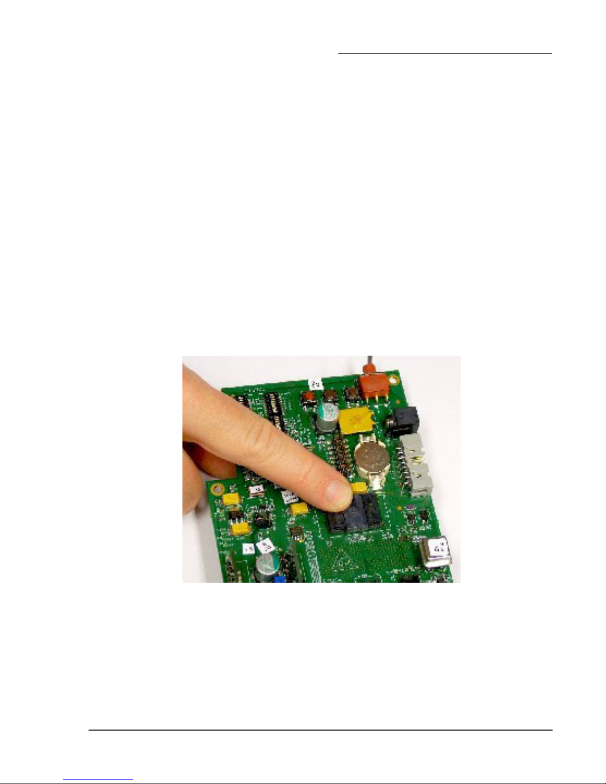
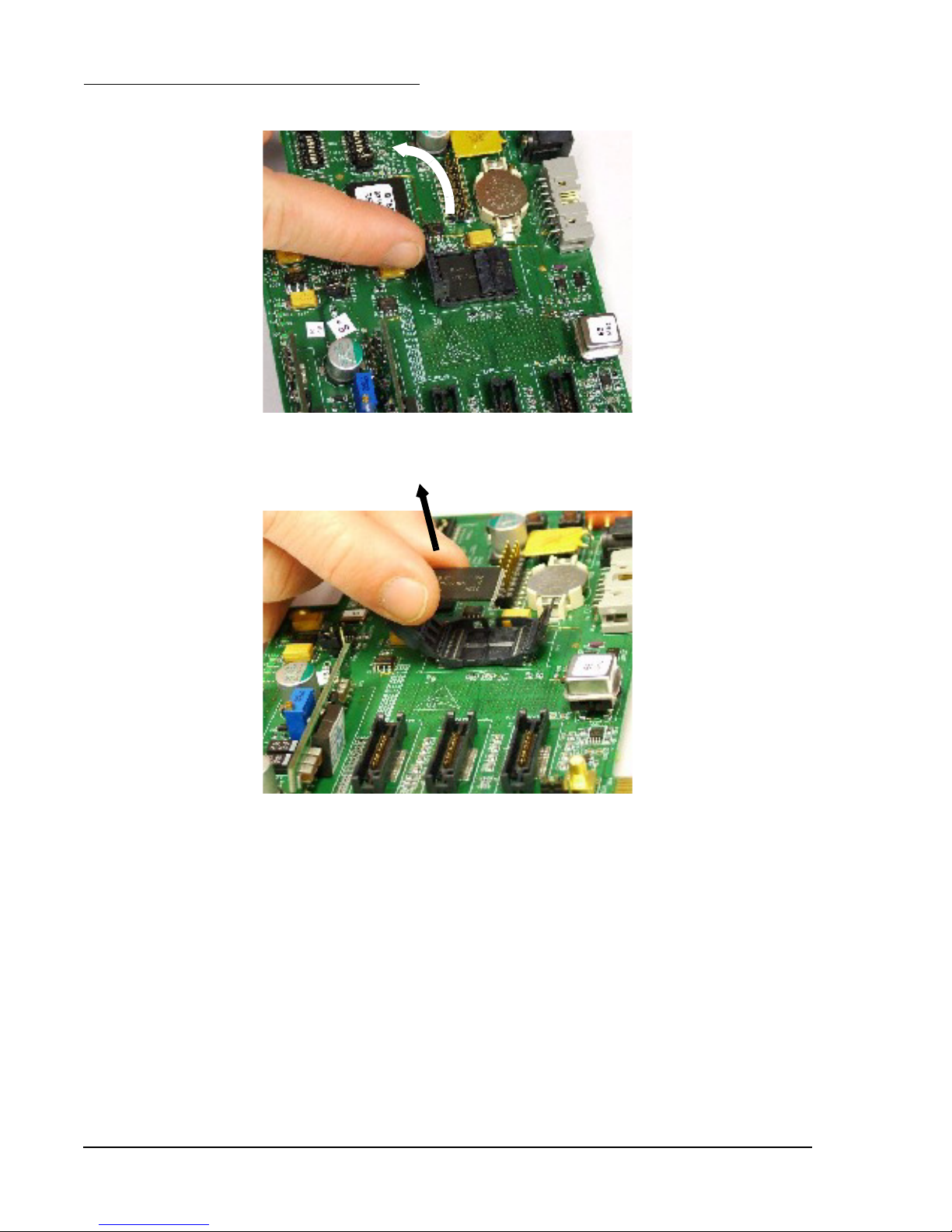
To remove the flash memory, follow the instructions below in Figure 7-1 to Figure 7-4 below (in
that order). Note that the flash memory can be changed no more than 50 times.
To replace the flash memory, follow the instructions in Figure 7-4 to Figure 7-1 (in that order),
then secure the casing as shown in Figure 7-5.
.
Figure 7-1 Flash Memory - push to dislodge casing
Freescale Semiconductor MPC8349E MDS Processor Board User’s Manual 53
Page 54
Replacing Devices
Figure 7-2 Flash Memory - open casing
Figure 7-3 Flash Memory - remove memory unit
54 MPC8349E MDS Processor Board User’s Manual Freescale Semiconductor
Page 55
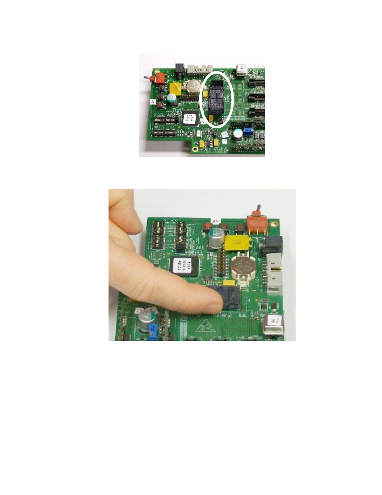
Figure 7-4 Flash Memory - unit removed
Replacing Devices
Figure 7-5 Flash Memory - replacing unit (push in until “click” is heard)
7.1.1 Cleaning Flash Memory
If there is some decrease in performance from the flash memory unit, the socket may need to be
cleaned. Do this by dipping a tooth pick dipped in isopropyl alcohol, and gently removing any
residual debris from the flash memory socket.
Freescale Semiconductor MPC8349E MDS Processor Board User’s Manual 55
Page 56
Replacing Devices
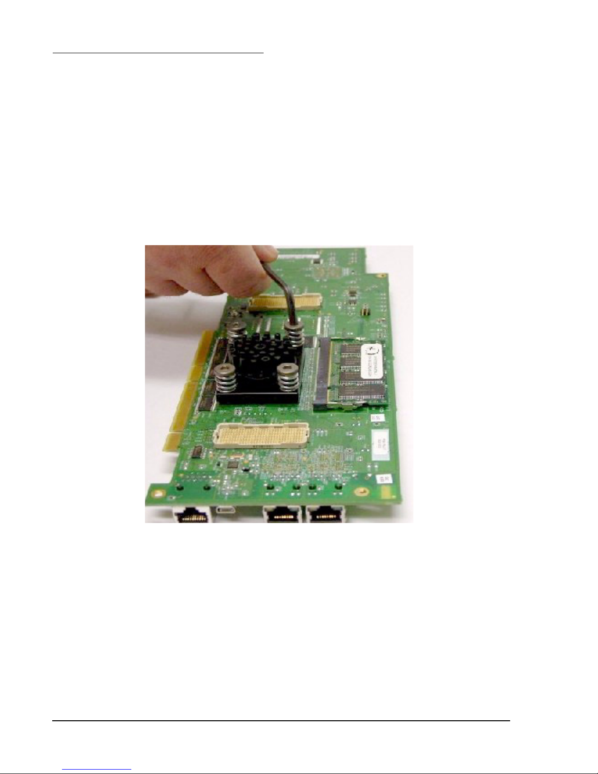
7.2 Replacing SODIMM units
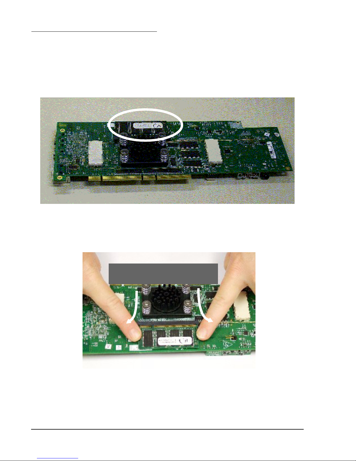
To remove or replace the SODIMM units, follow the instructions in Figure 7-6 through Figure 79, in that order.
Figure 7-6 SODIMM Memory - Location on underside of board
Press down and outwards
Figure 7-7 SODIMM Memory - release retaining clips
56 MPC8349E MDS Processor Board User’s Manual Freescale Semiconductor
Page 57
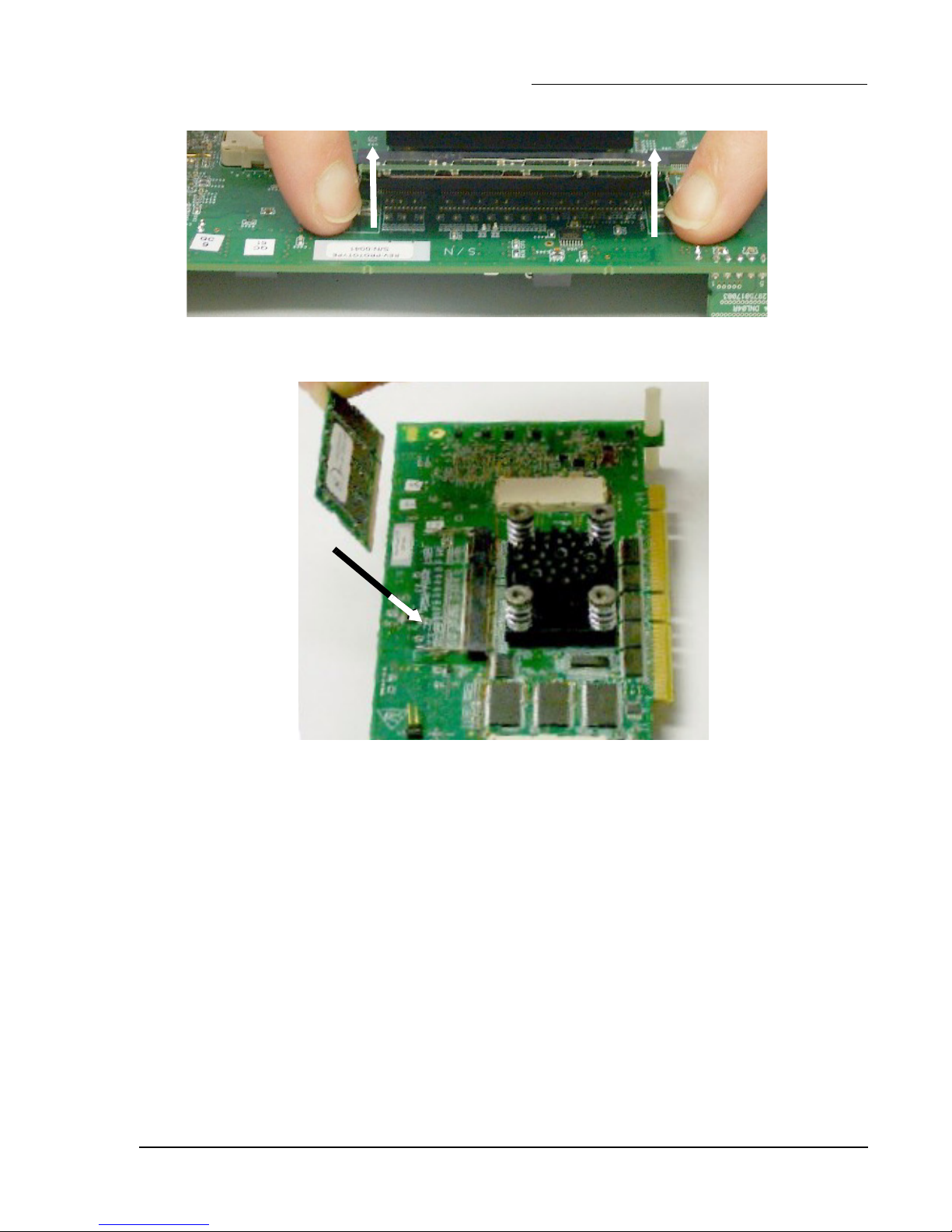
Unit pops up
Figure 7-8 SODIMM Memory - release unit
Replacing Devices
Figure 7-9 SODIMM Memory - remove unit
Freescale Semiconductor MPC8349E MDS Processor Board User’s Manual 57
Page 58
Replacing Devices
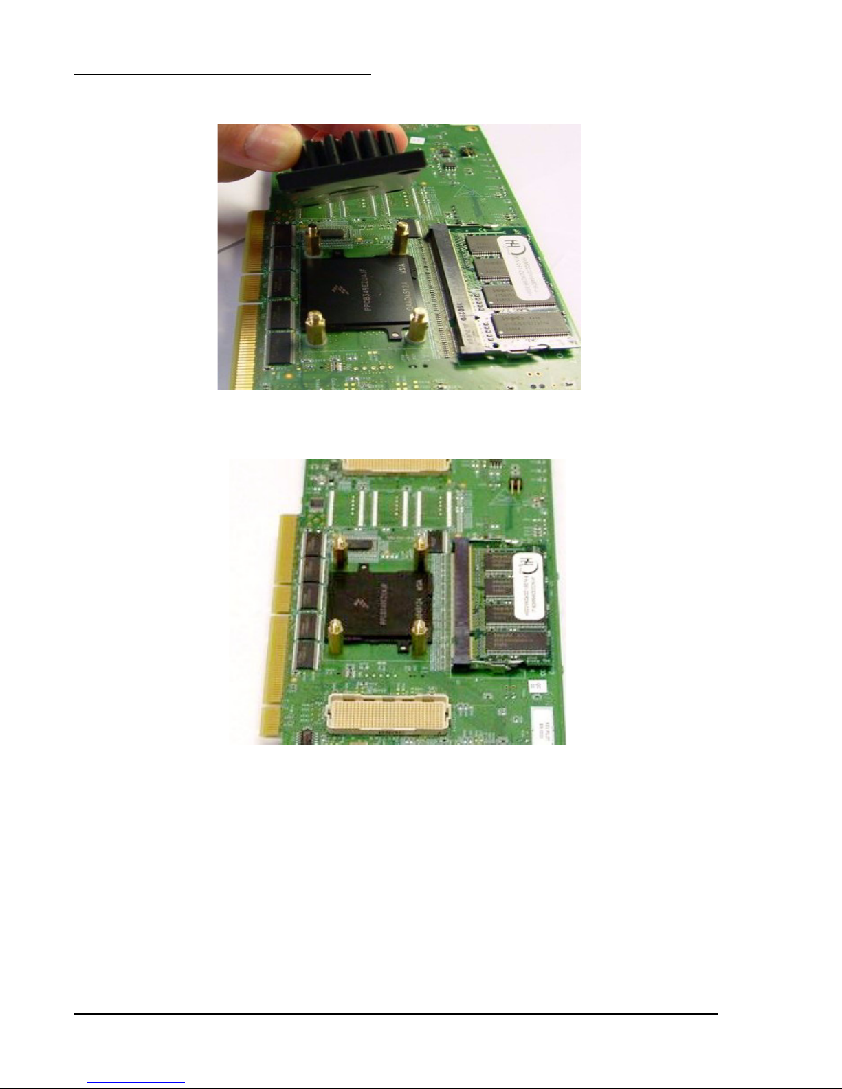
7.3 Replacing MSC8349E Processor
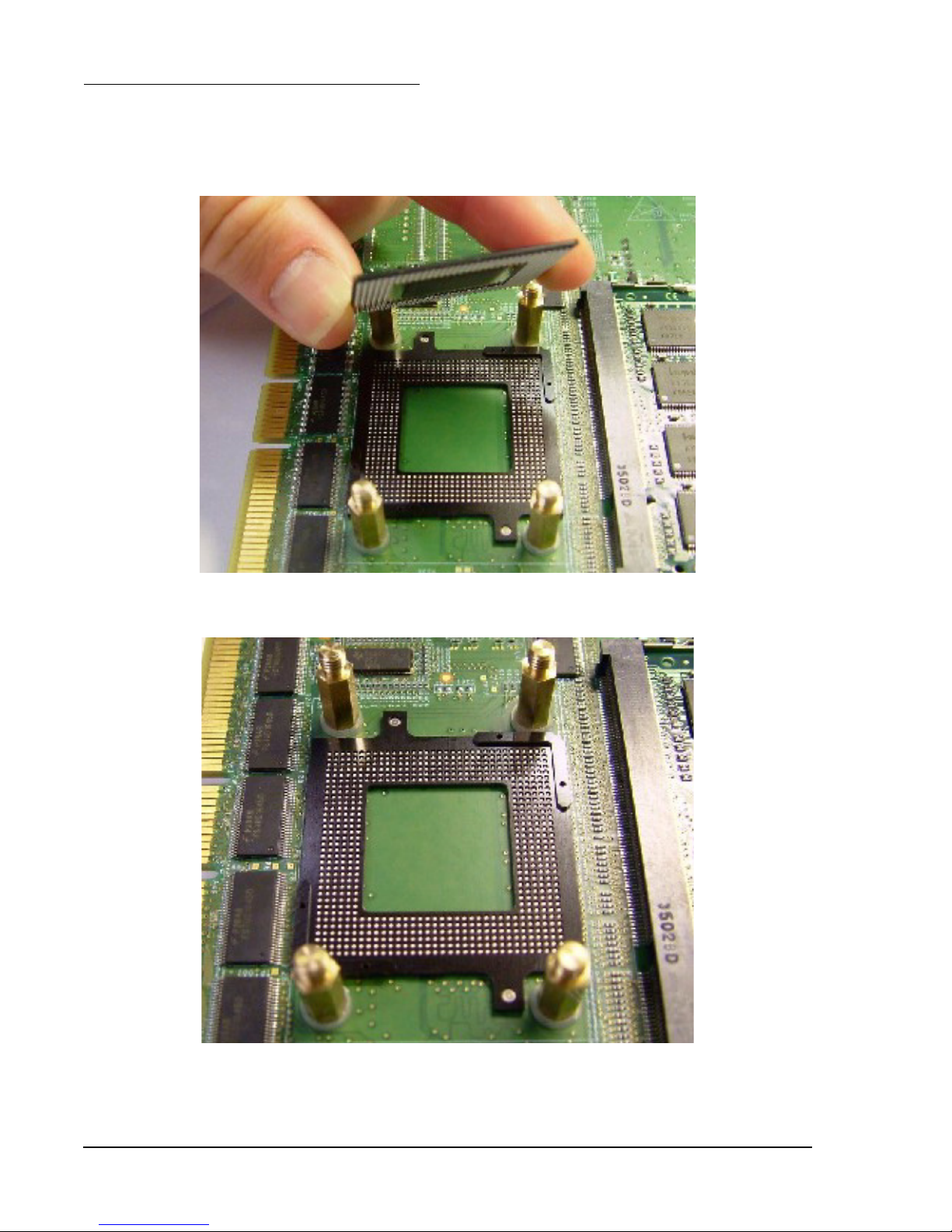
To remove the MSC8349E processor, follow the instructions in Figure 7-10 to Figure 7-19
below.
To replace the MSC8349E processor, follow the instructions in Figure 7-19 to Figure 7-10 below
(in that order).
Note that the Allen wrench is provided in the tool kit.
When replacing the framework of the chip, make sure that it is properly aligned as shown in
Figure 7-18. Incorrect alignment is shown in Figure 7-19.
Figure 7-10 Loosen Allen screws
58 MPC8349E MDS Processor Board User’s Manual Freescale Semiconductor
Page 59
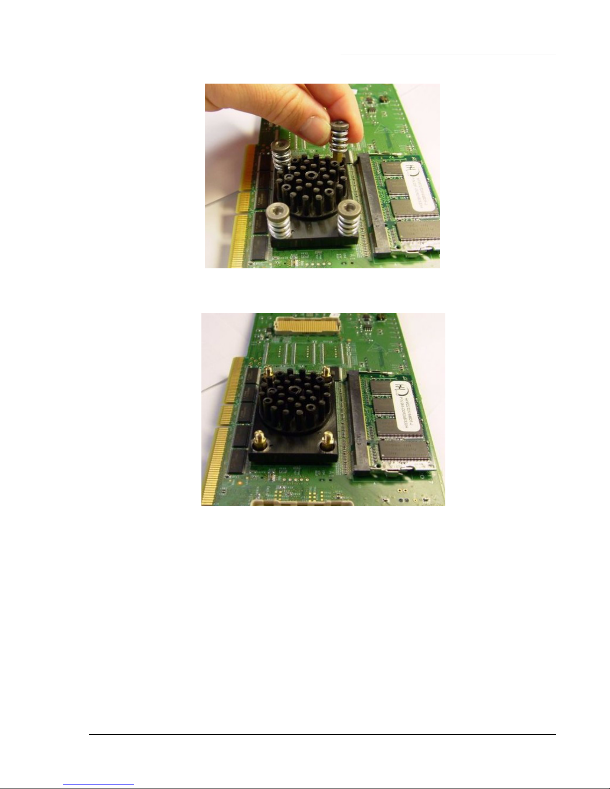
Figure 7-11 Remove Allen screws by hand
Replacing Devices
Freescale Semiconductor MPC8349E MDS Processor Board User’s Manual 59
Figure 7-12 Allen screws removed
Page 60
Replacing Devices
Figure 7-13 Remove heat sink
Figure 7-14 Heat sink removed
60 MPC8349E MDS Processor Board User’s Manual Freescale Semiconductor
Page 61
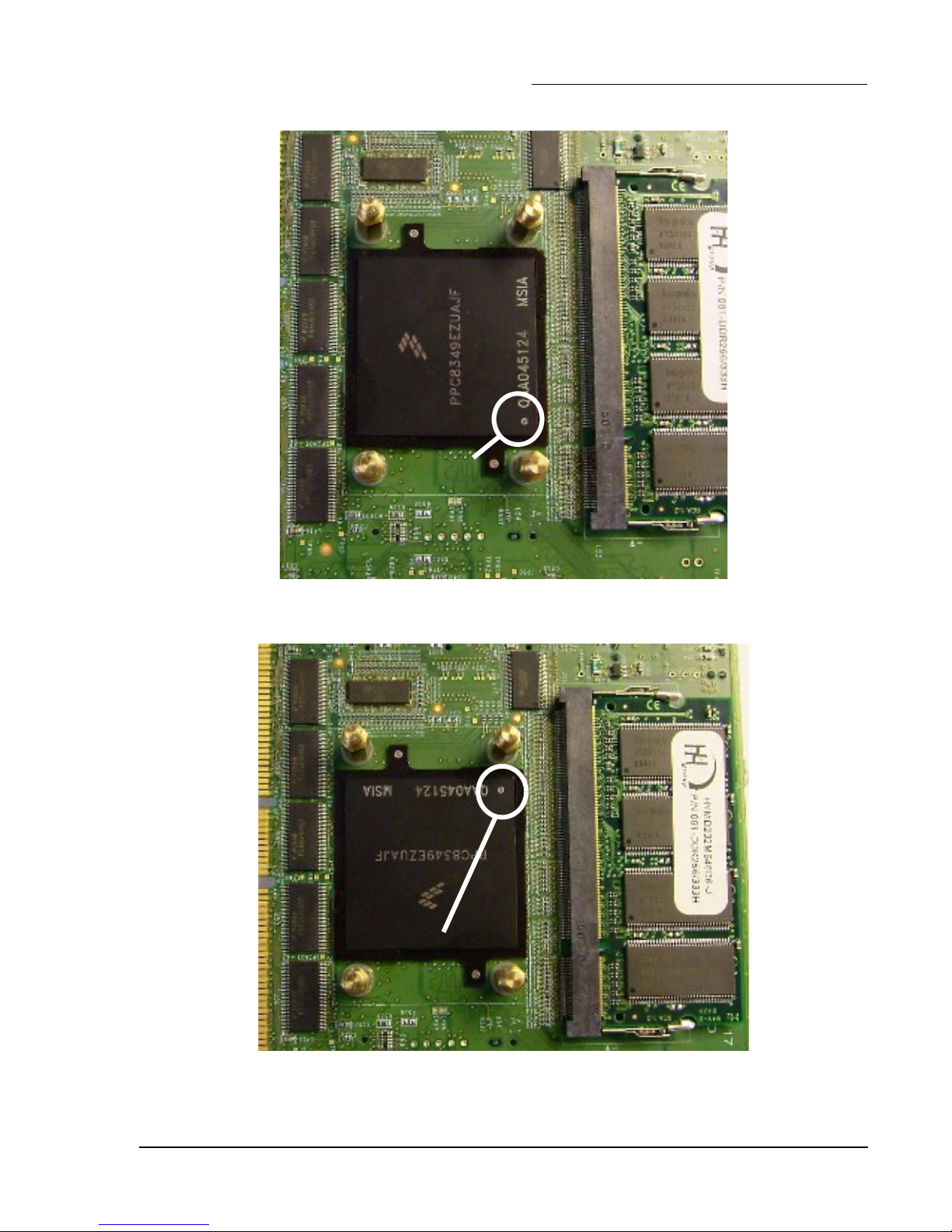
Alignment Indicator:
aligned correctly
Replacing Devices
Figure 7-15 Chip alignment: Correct
Alignment Indicator:
aligned incorrectly
Freescale Semiconductor MPC8349E MDS Processor Board User’s Manual 61
Figure 7-16 Chip alignment: Incorrect
Page 62
Replacing Devices
Figure 7-17 Remove chip
Background shows only green
Figure 7-18 Chip framework alignment: correct
62 MPC8349E MDS Processor Board User’s Manual Freescale Semiconductor
Page 63
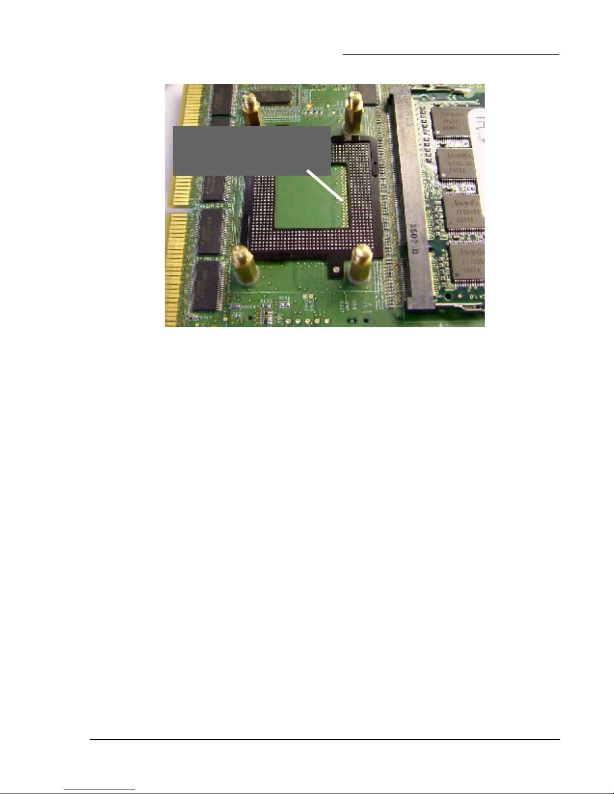
Background shows
underlying sockets
Replacing Devices
Figure 7-19 Chip framework alignment: incorrect
Freescale Semiconductor MPC8349E MDS Processor Board User’s Manual 63
Page 64

Replacing Devices
64 MPC8349E MDS Processor Board User’s Manual Freescale Semiconductor
 Loading...