

Page 1

MPC8308 PowerQUICC II Pro
Processor Reference Manual
MPC8308RM
Rev. 1
09/2013
Page 2

How to Reach Us:
Home Page:
www.freescale.com
Web Support:
http://www.freescale.com/support
Information in this document is provided solely to enable system and software
implementers to use Freescale products. There are no express or implied copyright
licenses granted hereunder to design or fabricate any integrated circuits based on the
information in this document.
Freescale reserves the right to make changes without further notice to any products
herein. Freescale makes no warranty, representation, or guarantee regarding the
suitability of its products for any pa rticular purpose, nor does Freescale assume any
liability arising out of the application or use of any product or circuit, and specifically
disclaims any and all liability, including without limitation consequential or incidental
damages. “Typical” parameters that may be provided in Freescale data sheets and/or
specifications can and do vary in different applications, and actua l performance may v ary
over time. All operat i ng parameters, including “typicals,” must be validated for each
customer application by customer’s technical experts. Freescale does not convey any
license under its patent rights nor the rights of othe rs. Freescale sells products pursuant
to standard terms and conditions of sale, which can be found at the following address:
freescale.com/SalesTermsandConditions.
Freescale, the Freescale logo, CodeWarrior, ColdFire, PowerQUICC,QorIQ,StarCore,
Symphony ,and VortiQa are trademarks of Freescale Semiconductor, Inc., Reg. U .S. P at.
& Tm. Off. CoreNet,and QUICC Engine are trademarks of F reescale Semicon ductor , Inc.
All other product or service names are the property of their respective owners. The P ower
Architecture and Po wer.org word marks and the Power and P ow er.org logos and related
marks are trademarks and service marks licensed by Power.org.
© 2010 and 2013 Freescale Semiconductor, Inc.
Document Number: MPC8308RM
Rev. 1, 09/2013
Page 3

Contents
Paragraph
Number Title
Page
Number
About This Book
Audience...................................................................................................................... lvii
Organization................................................................................................................. lvii
Suggested Reading........................................................................................................ lix
General Information.................................................................................................. lix
Related Documentation ............................................................................................ lix
Conventions................................................................................................................... lx
Signal Conventions....................................................................................................... lxi
Acronyms and Abbreviations ....................................................................................... lxi
Chapter 1
Overview
1.1 MPC8308 Overview ........................................................................................................ 1-1
1.2 MPC8308 Architecture Overview ................................................................................... 1-7
1.2.1 e300 Core.....................................................................................................................1-7
1.2.2 DDR2 Memory Controller......................................................................................... 1-10
1.2.3 Dual Enhanced Three-Speed Ethernet Controllers.................................................... 1-10
1.2.4 SerDes PHY............................................................................................................... 1-11
1.2.5 PCI Express Interface ................................................................................................ 1-11
1.2.6 Universal Serial Bus (USB) 2.0................................................................................. 1-11
1.2.7 Enhanced Local Bus Controller (eLBC).................................................................... 1-12
1.2.8 Integrated Programmable Interrupt Controller (IPIC)............................................... 1-14
2
1.2.9 I
C Interface............................................................................................................... 1-15
1.2.10 General Purpose DMA Controller............................................................................. 1-15
1.2.11 Dual Universal Asynchronous Receiver/Transmitter (DUART)............................... 1-16
1.2.12 Enhanced Secure Digital Host Controller (eSDHC).................................................. 1-16
1.2.13 System Timers ........................................................................................................... 1-17
Chapter 2
Signal Descriptions
2.1 Signals Overview.............................................................................................................2-1
2.2 Output Signal States During Reset ................................................................................ 2-13
MPC8308 PowerQUICC II Pro Processor Reference Manual, Rev. 1
Freescale Semiconductor iii
Page 4

Figures
Figure
Number Title
Page
Number
Chapter 3
Memory Map
3.1 Internal Memory-Mapped Registers................................................................................ 3-1
3.2 Accessing IMMR Memory from the Local Processor..................................................... 3-1
3.3 IMMR Address Map........................................................................................................ 3-1
Chapter 4
Reset, Clocking, and Initialization
4.1 External Signals............................................................................................................... 4-1
4.1.1 Reset Signals................................................................................................................ 4-1
4.1.2 Clock Signals............................................................................................................... 4-2
4.2 Functional Description..................................................................................................... 4-3
4.2.1 Reset Operations..........................................................................................................4-3
4.2.2 Power-On Reset Flow.................................................................................................. 4-5
4.2.3 Hard Reset Flow .......................................................................................................... 4-6
4.3 Reset Configuration......................................................................................................... 4-7
4.3.1 Reset Configuration Signals ........................................................................................ 4-7
4.3.2 Reset Configuration Words.......................................................................................... 4-9
4.3.3 Loading the Reset Configuration Words ................................................................... 4-16
4.4 Clocking ........................................................................................................................ 4-22
4.4.1 System Clock Domains.............................................................................................. 4-23
4.4.2 USB Clocking............................................................................................................ 4-24
4.4.3 Ethernet Clocking...................................................................................................... 4-25
4.5 Memory Map/Register Definitions................................................................................ 4-25
4.5.1 Reset Configuration Register Descriptions................................................................ 4-25
4.5.2 Clock Configuration Registers................................................................................... 4-29
Chapter 5
System Configuration
5.1 Local Memory Map Overview and Example .................................................................. 5-1
5.1.1 Address Translation and Mapping............................................................................... 5-3
5.1.2 Window into Configuration Space...............................................................................5-3
5.1.3 Local Access Windows................................................................................................ 5-4
5.1.4 Local Access Register Descriptions ............................................................................ 5-5
5.1.5 Precedence of Local Access Windows...................................................................... 5-13
5.1.6 Configuring Local Access Windows......................................................................... 5-13
5.1.7 Distinguishing Local Access Windows from Other Mapping Functions..................5-13
5.1.8 Outbound Address Translation and Mapping Windows............................................ 5-14
MPC8308 PowerQUICC II Pro Processor Reference Manual, Rev. 1
iv Freescale Semiconductor
Page 5

Figures
Figure
Number Title
Page
Number
5.1.9 Inbound Address Translation and Mapping Windows .............................................. 5-14
5.1.10 Internal Memory Map................................................................................................ 5-14
5.1.11 Accessing Internal Memory from External Masters.................................................. 5-15
5.2 System Configuration .................................................................................................... 5-15
5.2.1 System Configuration Register Memory Map........................................................... 5-15
5.2.2 System Configuration Registers ................................................................................ 5-16
5.3 Software Watchdog Timer (WDT)................................................................................. 5-32
5.3.1 WDT Overview.......................................................................................................... 5-32
5.3.2 WDT Features............................................................................................................ 5-33
5.3.3 WDT Modes of Operation......................................................................................... 5-33
5.3.4 WDT Memory Map/Register Definition ................................................................... 5-34
5.3.5 Functional Description............................................................................................... 5-37
5.3.6 Initialization/Application Information (WDT Programming Guidelines)................. 5-39
5.4 Real Time Clock (RTC) Module.................................................................................... 5-39
5.4.1 Overview.................................................................................................................... 5-39
5.4.2 Features...................................................................................................................... 5-40
5.4.3 Assumptions............................................................................................................... 5-40
5.4.4 Modes of operation.................................................................................................... 5-40
5.4.5 External Signal Description....................................................................................... 5-41
5.4.6 RTC Memory Map/Register Definition..................................................................... 5-41
5.4.7 Functional Description............................................................................................... 5-45
5.4.8 RTC Reset Sequence.................................................................................................. 5-47
5.4.9 RTC Initialization Sequence ...................................................................................... 5-47
5.5 Periodic Interval Timer (PIT) ........................................................................................ 5-47
5.5.1 PIT Overview............................................................................................................. 5-47
5.5.2 PIT Features...............................................................................................................5-48
5.5.3 PIT Modes of Operation............................................................................................ 5-48
5.5.4 PIT External Signal Description................................................................................ 5-48
5.5.5 PIT Memory Map/Register Definition ...................................................................... 5-49
5.5.6 Functional Description............................................................................................... 5-52
5.5.7 PIT Programming Guidelines.................................................................................... 5-53
5.6 General-Purpose Timers (GTMs)................................................................................... 5-53
5.6.1 GTM Overview.......................................................................................................... 5-53
5.6.2 GTM Features ............................................................................................................ 5-54
5.6.3 GTM Modes of Operation.......................................................................................... 5-55
5.6.4 GTM External Signal Description ............................................................................. 5-56
5.6.5 GTM Memory Map/Register Definition.................................................................... 5-57
5.6.6 Functional Description............................................................................................... 5-66
5.6.7 Initialization/Application Information (Programming Guidelines for GTM Registers)....
5-69
5.7 Power Management Control (PMC)..............................................................................5-69
MPC8308 PowerQUICC II Pro Processor Reference Manual, Rev. 1
Freescale Semiconductor v
Page 6

Figures
Figure
Number Title
Page
Number
5.7.1 External Signal Description....................................................................................... 5-70
5.7.2 PMC Memory Map/Register Definition.................................................................... 5-70
5.7.3 Functional Description............................................................................................... 5-71
Chapter 6
Arbiter and Bus Monitor
6.1 Overview.......................................................................................................................... 6-1
6.1.1 Coherent System Bus Overview.................................................................................. 6-1
6.2 Arbiter Memory Map/Register Definition....................................................................... 6-2
6.2.1 Arbiter Configuration Register (ACR)........................................................................ 6-3
6.2.2 Arbiter Timers Register (ATR) .................................................................................... 6-4
6.2.3 Arbiter Event Enable Register (AEER).......................................................................6-5
6.2.4 Arbiter Event Register (AER)...................................................................................... 6-6
6.2.5 Arbiter Interrupt Definition Register (AIDR).............................................................. 6-7
6.2.6 Arbiter Mask Register (AMR)..................................................................................... 6-8
6.2.7 Arbiter Event Attributes Register (AEATR)................................................................ 6-9
6.2.8 Arbiter Event Address Register (AEADR)................................................................ 6-10
6.2.9 Arbiter Event Response Register (AERR)................................................................. 6-11
6.3 Functional Description................................................................................................... 6-12
6.3.1 Arbitration Policy ...................................................................................................... 6-12
6.3.2 Bus Error Detection................................................................................................... 6-15
6.4 Initialization/Applications Information ......................................................................... 6-18
6.4.1 Initialization Sequence............................................................................................... 6-18
6.4.2 Error Handling Sequence........................................................................................... 6-18
Chapter 7
e300 Processor Core Overview
7.1 Overview.......................................................................................................................... 7-1
7.1.1 Features........................................................................................................................ 7-3
7.1.2 Instruction Unit............................................................................................................ 7-6
7.1.3 Independent Execution Units....................................................................................... 7-7
7.1.4 Completion Unit .......................................................................................................... 7-8
7.1.5 Memory Subsystem Support........................................................................................ 7-8
7.1.6 Bus Interface Unit (BIU) ........................................................................................... 7-10
7.1.7 System Support Functions......................................................................................... 7-11
7.2 e300 Processor and System Version Numbers............................................................... 7-13
7.3 PowerPC Architecture Implementation......................................................................... 7-13
7.4 Implementation-Specific Information............................................................................ 7-14
7.4.1 Register Model........................................................................................................... 7-14
MPC8308 PowerQUICC II Pro Processor Reference Manual, Rev. 1
vi Freescale Semiconductor
Page 7

Figures
Figure
Number Title
Page
Number
7.4.2 Instruction Set and Addressing Modes...................................................................... 7-26
7.4.3 Cache Implementation............................................................................................... 7-29
7.4.4 Interrupt Model.......................................................................................................... 7-31
7.4.5 Memory Management................................................................................................ 7-35
7.4.6 Instruction Timing ..................................................................................................... 7-36
7.4.7 Core Interface ............................................................................................................ 7-37
7.4.8 Debug Features ......................................................................................................... 7-39
7.5 Differences Between Cores........................................................................................... 7-40
Chapter 8
Integrated Programmable Interrupt Controller (IPIC)
8.1 Introduction...................................................................................................................... 8-1
8.2 Features............................................................................................................................ 8-4
8.3 Modes of Operation ......................................................................................................... 8-4
8.3.1 Core Enable Mode....................................................................................................... 8-4
8.3.2 Core Disable Mode...................................................................................................... 8-4
8.4 External Signal Description............................................................................................. 8-5
8.4.1 Overview...................................................................................................................... 8-5
8.4.2 Detailed Signal Descriptions ....................................................................................... 8-5
8.5 Memory Map/Register Definition ................................................................................... 8-6
8.5.1 System Global Interrupt Configuration Register (SICFR).......................................... 8-8
8.5.2 System Global Interrupt Vector Register (SIVCR)...................................................... 8-9
8.5.3 System Internal Interrupt Pending Registers (SIPNR_H and SIPNR_L).................. 8-12
8.5.4 System Internal Interrupt Group A Priority Register (SIPRR_A)............................. 8-14
8.5.5 System Internal Interrupt Group B Priority Register (SIPRR_B) ............................. 8-15
8.5.6 System Internal Interrupt Group C Priority Register (SIPRR_C) ............................. 8-16
8.5.7 System Internal Interrupt Group D Priority Register (SIPRR_D)............................. 8-16
8.5.8 System Internal Interrupt Mask Register (SIMSR_H and SIMSR_L)...................... 8-17
8.5.9 System Internal Interrupt Control Register (SICNR)................................................ 8-18
8.5.10 System External Interrupt Pending Register (SEPNR).............................................. 8-20
8.5.11 System Mixed Interrupt Group A Priority Register (SMPRR_A)............................. 8-21
8.5.12 System Mixed Interrupt Group B Priority Register (SMPRR_B)............................. 8-22
8.5.13 System External Interrupt Mask Register (SEMSR)................................................. 8-22
8.5.14 System External Interrupt Control Register (SECNR).............................................. 8-23
8.5.15 System Error Status Register (SERSR)..................................................................... 8-25
8.5.16 System Error Mask Register (SERMR)..................................................................... 8-25
8.5.17 System Error Control Register (SERCR) .................................................................. 8-26
8.5.18 System External interrupt Polarity Control Register (SEPCR)................................. 8-26
8.5.19 System Internal Interrupt Force Registers (SIFCR_H and SIFCR_L)...................... 8-27
8.5.20 System External Interrupt Force Register (SEFCR).................................................. 8-29
MPC8308 PowerQUICC II Pro Processor Reference Manual, Rev. 1
Freescale Semiconductor vii
Page 8

Figures
Figure
Number Title
Page
Number
8.5.21 System Error Force Register (SERFR)...................................................................... 8-29
8.5.22 System Critical Interrupt Vector Register (SCVCR)................................................. 8-30
8.5.23 System Management Interrupt Vector Register (SMVCR) ....................................... 8-30
8.6 Functional Description................................................................................................... 8-31
8.6.1 Interrupt Types........................................................................................................... 8-31
8.6.2 Interrupt Configuration.............................................................................................. 8-32
8.6.3 Internal Interrupts Group Relative Priority................................................................ 8-33
8.6.4 Mixed Interrupts Group Relative Priority.................................................................. 8-33
8.6.5 Highest Priority Interrupt........................................................................................... 8-34
8.6.6 Interrupt Source Priorities.......................................................................................... 8-34
8.6.7 Masking Interrupt Sources......................................................................................... 8-38
8.6.8 Interrupt Vector Generation and Calculation............................................................. 8-39
8.6.9 Machine Check Interrupts.......................................................................................... 8-39
8.7 Message Shared Interrupts............................................................................................. 8-40
8.7.1 Memory Map/Register Definition ............................................................................. 8-40
8.7.2 Message Shared Registers ......................................................................................... 8-40
Chapter 9
DDR Memory Controller
9.1 Introduction...................................................................................................................... 9-1
9.2 Features............................................................................................................................ 9-2
9.2.1 Modes of Operation..................................................................................................... 9-3
9.3 External Signal Descriptions ........................................................................................... 9-3
9.3.1 Signals Overview......................................................................................................... 9-3
9.3.2 Detailed Signal Descriptions ....................................................................................... 9-6
9.4 Memory Map/Register Definition ................................................................................... 9-9
9.4.1 Register Descriptions................................................................................................. 9-10
9.5 Functional Description................................................................................................... 9-38
9.5.1 DDR SDRAM Interface Operation............................................................................ 9-42
9.5.2 DDR SDRAM Address Multiplexing........................................................................ 9-43
9.5.3 JEDEC Standard DDR SDRAM Interface Commands............................................. 9-45
9.5.4 DDR SDRAM Interface Timing................................................................................ 9-47
9.5.5 DDR SDRAM Mode-Set Command Timing............................................................. 9-51
9.5.6 DDR SDRAM Registered DIMM Mode................................................................... 9-51
9.5.7 DDR SDRAM Write Timing Adjustments................................................................ 9-52
9.5.8 DDR SDRAM Refresh .............................................................................................. 9-53
9.5.9 DDR Data Beat Ordering........................................................................................... 9-56
9.5.10 Page Mode and Logical Bank Retention ................................................................... 9-57
9.5.11 Error Checking and Correcting (ECC) ...................................................................... 9-58
9.5.12 Error Management..................................................................................................... 9-60
MPC8308 PowerQUICC II Pro Processor Reference Manual, Rev. 1
viii Freescale Semiconductor
Page 9

Figures
Figure
Number Title
Page
Number
9.6 Initialization/Application Information........................................................................... 9-60
9.6.1 DDR SDRAM Initialization Sequence...................................................................... 9-62
Chapter 10
Enhanced Local Bus Controller
10.1 Introduction.................................................................................................................... 10-1
10.1.1 Overview.................................................................................................................... 10-2
10.1.2 Features...................................................................................................................... 10-2
10.1.3 Modes of Operation................................................................................................... 10-3
10.2 External Signal Descriptions ......................................................................................... 10-4
10.3 Memory Map/Register Definition ................................................................................. 10-7
10.3.1 Register Descriptions................................................................................................. 10-9
10.4 Functional Description................................................................................................. 10-39
10.4.1 Basic Architecture.................................................................................................... 10-40
10.4.2 General-Purpose Chip-Select Machine (GPCM)..................................................... 10-42
10.4.3 Flash Control Machine (FCM) ................................................................................ 10-53
10.4.4 User-Programmable Machines (UPMs)................................................................... 10-68
10.5 Initialization/Application Information......................................................................... 10-84
10.5.1 Interfacing to Peripherals in Different Address Modes........................................... 10-84
10.5.2 Interface to Different Port-Size Devices.................................................................. 10-85
10.5.3 Command Sequence Examples for NAND Flash EEPROM................................... 10-86
10.5.4 Interfacing to Fast-Page Mode DRAM Using UPM ............................................... 10-90
10.5.5 Interfacing to ZBT SRAM Using UPM................................................................. 10-100
Chapter 11
Enhanced Secure Digital Host Controller
11.1 Overview........................................................................................................................ 11-1
11.2 Features.......................................................................................................................... 11-3
11.2.1 Data Transfer Modes.................................................................................................. 11-4
11.3 External Signal Description........................................................................................... 11-4
11.4 Memory Map/Register Definition ................................................................................. 11-5
11.4.1 DMA System Address Register (DSADDR)............................................................. 11-7
11.4.2 Block Attributes Register (BLKATTR)..................................................................... 11-7
11.4.3 Command Argument Register (CMDARG).............................................................. 11-8
11.4.4 Transfer Type Register (XFERTYP).......................................................................... 11-9
11.4.5 Command Response 0–3 (CMDRSP0–3)................................................................ 11-12
11.4.6 Buffer Data Port Register (DATPORT)................................................................... 11-14
11.4.7 Present State Register (PRSSTAT) .......................................................................... 11-15
11.4.8 Protocol Control Register (PROCTL) ..................................................................... 11-19
MPC8308 PowerQUICC II Pro Processor Reference Manual, Rev. 1
Freescale Semiconductor ix
Page 10

Figures
Figure
Number Title
Page
Number
11.4.9 System Control Register (SYSCTL)........................................................................ 11-22
11.4.10 Interrupt Status Register (IRQSTAT)....................................................................... 11-24
11.4.11 Interrupt Status Enable Register (IRQSTATEN)..................................................... 11-28
11.4.12 Interrupt Signal Enable Register (IRQSIGEN) ....................................................... 11-31
11.4.13 Auto CMD12 Error Status Register (AUTOC12ERR)............................................ 11-33
11.4.14 Host Controller Capabilities (HOSTCAPBLT) ....................................................... 11-35
11.4.15 Watermark Level Register (WML).......................................................................... 11-36
11.4.16 Force Event Register (FEVT).................................................................................. 11-36
11.4.17 Host Controller Version Register (HOSTVER)....................................................... 11-38
11.4.18 DMA Control Register (DCR)................................................................................. 11-38
11.5 Functional Description................................................................................................. 11-38
11.5.1 Data Buffer .............................................................................................................. 11-39
11.5.2 DMA CSB Interface ................................................................................................ 11-41
11.5.3 SD Protocol Unit...................................................................................................... 11-42
11.5.4 Clock & Reset Manager........................................................................................... 11-44
11.5.5 Clock Generator....................................................................................................... 11-44
11.5.6 SDIO Card Interrupt ................................................................................................ 11-44
11.5.7 Card Insertion and Removal Detection.................................................................... 11-46
11.5.8 Power Management ................................................................................................. 11-46
11.6 Initialization/Application Information......................................................................... 11-47
11.6.1 Command Send and Response Receive Basic Operation........................................ 11-47
11.6.2 Card Identification Mode......................................................................................... 11-48
11.6.3 Card Access ............................................................................................................. 11-52
11.6.4 Switch Function....................................................................................................... 11-57
11.6.5 Commands for MMC/SD/SDIO.............................................................................. 11-60
11.7 Software Restrictions................................................................................................... 11-65
11.7.1 Initialization Active ................................................................................................. 11-65
11.7.2 Software Polling Procedure..................................................................................... 11-65
11.7.3 Suspend Operation................................................................................................... 11-65
11.7.4 Data Port Access...................................................................................................... 11-65
11.7.5 Multi-block Read..................................................................................................... 11-65
Chapter 12
DMA Controller (DMAC)
12.1 Overview........................................................................................................................ 12-1
12.1.1 Features...................................................................................................................... 12-2
12.2 DMAC Memory Map/Register Definition .................................................................... 12-2
12.2.1 DMA Control Register (DMACR)............................................................................ 12-3
12.3 DMA Error Status (DMAES) ........................................................................................ 12-6
12.3.1 DMA Enable Error Interrupt Register (DMAEEI)....................................................12-8
MPC8308 PowerQUICC II Pro Processor Reference Manual, Rev. 1
x Freescale Semiconductor
Page 11

Figures
Figure
Number Title
Page
Number
12.3.2 DMA Set Enable Error Interrupt (DMASEEI).......................................................... 12-9
12.3.3 DMA Clear Enable Error Interrupt (DMACEEI)...................................................... 12-9
12.3.4 DMA Clear Interrupt Request (DMACINT)........................................................... 12-10
12.3.5 DMA Clear Error (DMACERR).............................................................................. 12-11
12.3.6 DMA Set START Bit (DMASSRT)......................................................................... 12-11
12.3.7 DMA Clear DONE Status (DMACDNE)................................................................ 12-12
12.3.8 DMA Interrupt Request Register (DMAINT)......................................................... 12-12
12.3.9 DMA Error Register (DMAERR)............................................................................ 12-13
12.3.10 DMA General Purpose Output Register (DMAGPOR) .......................................... 12-14
12.3.11 DMA Channel n Priority (DCHPRIn), n = 0–15..................................................... 12-15
12.3.12 Transfer Control Descriptor (TCD)......................................................................... 12-16
12.4 Functional Description................................................................................................. 12-24
12.4.1 DMA Microarchitecture .......................................................................................... 12-24
12.4.2 DMA Basic Data Flow ............................................................................................ 12-25
12.5 Initialization/Application Information......................................................................... 12-28
12.5.1 DMA Initialization................................................................................................... 12-28
12.5.2 DMA Programming Errors...................................................................................... 12-29
12.6 DMA Transfer.............................................................................................................. 12-29
12.6.1 Single Request ......................................................................................................... 12-29
12.6.2 Multiple Requests.................................................................................................... 12-30
12.7 TCD Status................................................................................................................... 12-32
12.7.1 Minor Loop Complete ............................................................................................. 12-32
12.7.2 Active Channel TCD Reads..................................................................................... 12-32
12.7.3 Preemption status..................................................................................................... 12-32
12.8 Channel Linking .......................................................................................................... 12-33
12.9 Programming during channel execution...................................................................... 12-33
12.9.1 Dynamic priority changing...................................................................................... 12-33
12.9.2 Dynamic channel linking and dynamic scatter/gather............................................. 12-34
Chapter 13
Universal Serial Bus Interface
13.1 Introduction.................................................................................................................... 13-1
13.1.1 Overview.................................................................................................................... 13-2
13.1.2 Features...................................................................................................................... 13-2
13.1.3 Modes of Operation................................................................................................... 13-2
13.2 External Signals............................................................................................................. 13-3
13.2.1 ULPI Interface ........................................................................................................... 13-3
13.3 Memory Map/Register Definitions................................................................................ 13-4
13.3.1 Capability Registers................................................................................................... 13-6
13.3.2 Operational Registers............................................................................................... 13-10
MPC8308 PowerQUICC II Pro Processor Reference Manual, Rev. 1
Freescale Semiconductor xi
Page 12

Figures
Figure
Number Title
Page
Number
13.4 Functional Description................................................................................................. 13-44
13.4.1 System Interface ...................................................................................................... 13-44
13.4.2 DMA Engine............................................................................................................ 13-45
13.4.3 FIFO RAM Controller............................................................................................. 13-45
13.4.4 PHY Interface.......................................................................................................... 13-45
13.5 Host Data Structures.................................................................................................... 13-45
13.5.1 Periodic Frame List.................................................................................................. 13-46
13.5.2 Asynchronous List Queue Head Pointer.................................................................. 13-47
13.5.3 Isochronous (High-Speed) Transfer Descriptor (iTD)............................................. 13-48
13.5.4 Split Transaction Isochronous Transfer Descriptor (siTD)...................................... 13-52
13.5.5 Queue Element Transfer Descriptor (qTD)............................................................. 13-56
13.5.6 Queue Head.............................................................................................................. 13-62
13.5.7 Periodic Frame Span Traversal Node (FSTN)......................................................... 13-66
13.6 Host Operations ........................................................................................................... 13-68
13.6.1 Host Controller Initialization................................................................................... 13-68
13.6.2 Power Port................................................................................................................ 13-69
13.6.3 Reporting Over-Current........................................................................................... 13-69
13.6.4 Suspend/Resume...................................................................................................... 13-69
13.6.5 Schedule Traversal Rules......................................................................................... 13-72
13.6.6 Periodic Schedule Frame Boundaries vs. Bus Frame Boundaries........................... 13-73
13.6.7 Periodic Schedule .................................................................................................... 13-75
13.6.8 Managing Isochronous Transfers Using iTDs.........................................................13-76
13.6.9 Asynchronous Schedule........................................................................................... 13-81
13.6.10 Managing Control/Bulk/Interrupt Transfers via Queue Heads................................ 13-85
13.6.11 Ping Control............................................................................................................. 13-89
13.6.12 Split Transactions.....................................................................................................13-90
13.6.13 Port Test Modes ..................................................................................................... 13-118
13.6.14 Interrupts................................................................................................................ 13-119
13.7 Device Data Structures .............................................................................................. 13-123
13.7.1 Endpoint Queue Head............................................................................................ 13-124
13.7.2 Endpoint Transfer Descriptor (dTD) ..................................................................... 13-127
13.8 Device Operational Model......................................................................................... 13-129
13.8.1 Device Controller Initialization............................................................................. 13-129
13.8.2 Port State and Control............................................................................................ 13-130
13.8.3 Managing Endpoints..............................................................................................13-133
13.8.4 Managing Queue Heads......................................................................................... 13-143
13.8.5 Managing Transfers with Transfer Descriptors ..................................................... 13-145
13.8.6 Servicing Interrupts................................................................................................ 13-148
13.9 Deviations from the EHCI Specifications ................................................................. 13-149
13.9.1 Embedded Transaction Translator Function.......................................................... 13-150
13.9.2 Device Operation................................................................................................... 13-153
MPC8308 PowerQUICC II Pro Processor Reference Manual, Rev. 1
xii Freescale Semiconductor
Page 13

Figures
Figure
Number Title
Page
Number
13.9.3 Non-Zero Fields the Register File ......................................................................... 13-154
13.9.4 SOF Interrupt......................................................................................................... 13-154
13.9.5 Embedded Design.................................................................................................. 13-154
13.9.6 Miscellaneous Variations from EHCI.................................................................... 13-154
13.10 Timing Diagrams....................................................................................................... 13-156
Chapter 14
PCI Express Interface Controller
14.1 Introduction.................................................................................................................... 14-1
14.1.1 MPC8308 as a PCI Express Initiator......................................................................... 14-3
14.1.2 MPC8308 as a PCI Express Target............................................................................ 14-3
14.1.3 Features...................................................................................................................... 14-4
14.1.4 Modes of Operation................................................................................................... 14-4
14.2 External Signal Descriptions ......................................................................................... 14-5
14.3 Memory Map/Register Definitions................................................................................ 14-5
14.3.1 PCI Express Memory Map ........................................................................................ 14-5
14.4 PCI Express Core Configuration Header Registers..................................................... 14-14
14.4.1 Common PCI Express-Compatible Configuration Header Registers...................... 14-14
14.4.2 Type 0 PCI Express-Compatible Configuration Header Registers.......................... 14-21
14.4.3 Type 1 PCI-Compatible Configuration Header Registers ....................................... 14-27
14.4.4 PCI Express-Compatible Device-Specific Configuration Space Registers............. 14-36
14.4.5 PCI Express Extended Configuration Space ........................................................... 14-52
14.4.6 PCI Express Controller Internal Control and Status Registers (CSRs)................... 14-62
14.4.7 PCI Express BAR Configuration Registers (EP Mode) .......................................... 14-72
14.4.8 PCI Express Extended Status and Control Registers............................................... 14-74
14.5 PCI Express CSB Bridge............................................................................................. 14-76
14.5.1 PCI Express CSB Bridge Configuration Space....................................................... 14-77
14.5.2 Global Registers....................................................................................................... 14-77
14.5.3 PCI Express Outbound PIO Registers..................................................................... 14-80
14.5.4 PCI Express Inbound PIO Registers........................................................................ 14-82
14.5.5 DMA Registers........................................................................................................ 14-83
14.5.6 Mailbox Registers.................................................................................................... 14-88
14.5.7 PCI Express Host Interrupt Registers...................................................................... 14-90
14.5.8 CSB System Interrupt Registers.............................................................................. 14-94
14.5.9 PCI Express Power Management Registers........................................................... 14-103
14.5.10 PCI Express Outbound Address Mapping Registers............................................. 14-104
14.5.11 PCI Express EP Inbound Address Translation Registers ...................................... 14-107
14.5.12 PCI Express RC Inbound Address Mapping Registers ......................................... 14-108
14.6 Functional Description................................................................................................14-111
14.6.1 Architecture ........................................................................................................... 14-112
MPC8308 PowerQUICC II Pro Processor Reference Manual, Rev. 1
Freescale Semiconductor xiii
Page 14

Figures
Figure
Number Title
Page
Number
14.6.2 Interrupts............................................................................................................... 14-122
14.6.3 Mailbox.................................................................................................................. 14-124
14.6.4 Power Management ............................................................................................... 14-126
14.6.5 Hot Reset................................................................................................................ 14-127
14.7 Initialization/Application Information....................................................................... 14-127
14.7.1 Initialization Sequence........................................................................................... 14-127
14.8 DMA Functional Operation....................................................................................... 14-128
14.8.1 DMA Descriptor Format........................................................................................ 14-128
14.8.2 Write DMA............................................................................................................ 14-130
14.8.3 Read DMA............................................................................................................. 14-131
14.8.4 Descriptor-Based DMA......................................................................................... 14-132
Chapter 15
SerDes PHY
15.1 Introduction.................................................................................................................... 15-1
15.1.1 Overview.................................................................................................................... 15-1
15.1.2 Features...................................................................................................................... 15-1
15.1.3 Mode of Operation..................................................................................................... 15-2
15.1.4 Clock.......................................................................................................................... 15-2
15.2 External Signals............................................................................................................. 15-2
15.3 Memory Map/Registers ................................................................................................. 15-3
15.3.1 SerDes Control Register 0 (SRDSCR0) .................................................................... 15-4
15.3.2 SerDes Control Register 1 (SRDSCR1) .................................................................... 15-6
15.3.3 SerDes Control Register 2 (SRDSCR2) .................................................................... 15-7
15.3.4 SerDes Control Register 3 (SRDSCR3) .................................................................... 15-8
15.3.5 SerDes Control Register 4 (SRDSCR4) .................................................................... 15-9
15.3.6 SerDesn Reset Control Register (SRDSRSTCTL).................................................. 15-10
15.4 Initialization Sequence and Reset................................................................................ 15-10
15.5 Power Management: Power Down .............................................................................. 15-11
Chapter 16
Enhanced Three-Speed Ethernet Controllers
16.1 Overview........................................................................................................................ 16-1
16.2 Features.......................................................................................................................... 16-2
16.3 Modes of Operation ....................................................................................................... 16-4
16.4 External Signals Description ......................................................................................... 16-5
16.4.1 Detailed Signal Descriptions ..................................................................................... 16-7
16.5 Memory Map/Register Definition ................................................................................. 16-9
16.5.1 Top-Level Module Memory Map ............................................................................ 16-10
MPC8308 PowerQUICC II Pro Processor Reference Manual, Rev. 1
xiv Freescale Semiconductor
Page 15

Figures
Figure
Number Title
Page
Number
16.5.2 Detailed Memory Map............................................................................................. 16-10
16.5.3 Memory-Mapped Register Descriptions.................................................................. 16-21
16.6 Functional Description............................................................................................... 16-120
16.6.1 Connecting to Physical Interfaces on Ethernet...................................................... 16-121
16.6.2 Gigabit Ethernet Controller Channel Operation.................................................... 16-124
16.6.3 TCP/IP Off-Load ................................................................................................... 16-139
16.6.4 Quality of Service (QoS) Provision....................................................................... 16-144
16.6.5 Lossless Flow Control ........................................................................................... 16-154
16.6.6 Hardware Assist for IEEE Std. 1588 Compliant Ti mestamping ........................... 16-157
16.6.7 Buffer Descriptors.................................................................................................. 16-164
16.7 Initialization/Application Information....................................................................... 16-171
16.7.1 Interface Mode Configuration ............................................................................... 16-172
16.7.2 MAC: Half-Duplex Collision on FCS of Short Frame.......................................... 16-178
Chapter 17
I2C Interface
17.1 Introduction.................................................................................................................... 17-1
17.1.1 Features...................................................................................................................... 17-2
17.1.2 Modes of Operation................................................................................................... 17-2
17.2 External Signal Descriptions ......................................................................................... 17-3
17.2.1 Signal Overview ........................................................................................................ 17-3
17.2.2 Detailed Signal Descriptions ..................................................................................... 17-3
17.3 Memory Map/Register Definition ................................................................................. 17-4
17.3.1 Register Descriptions................................................................................................. 17-5
17.4 Functional Description................................................................................................. 17-10
17.4.1 Transaction Protocol................................................................................................17-10
17.4.2 Arbitration Procedure .............................................................................................. 17-14
17.4.3 Handshaking ............................................................................................................ 17-15
17.4.4 Clock Control........................................................................................................... 17-15
17.4.5 Boot Sequencer Mode.............................................................................................. 17-16
17.5 Initialization/Application Information......................................................................... 17-21
17.5.1 Interrupt Service Routine Flowchart........................................................................ 17-21
17.5.2 Initialization Sequence............................................................................................. 17-23
17.5.3 Generation of START.............................................................................................. 17-23
17.5.4 Post-Transfer Software Response............................................................................ 17-23
17.5.5 Generation of STOP................................................................................................. 17-24
17.5.6 Generation of Repeated START.............................................................................. 17-24
17.5.7 Generation of SCL When SDA is Negated ............................................................. 17-24
17.5.8 Slave Mode Interrupt Service Routine..................................................................... 17-24
MPC8308 PowerQUICC II Pro Processor Reference Manual, Rev. 1
Freescale Semiconductor xv
Page 16

Figures
Figure
Number Title
Page
Number
Chapter 18
DUART
18.1 Overview........................................................................................................................ 18-1
18.1.1 Features...................................................................................................................... 18-2
18.1.2 Modes of Operation................................................................................................... 18-2
18.2 External Signal Descriptions ......................................................................................... 18-3
18.2.1 Signal Overview ........................................................................................................ 18-3
18.2.2 Detailed Signal Descriptions ..................................................................................... 18-3
18.3 Memory Map/Register Definition ................................................................................. 18-3
18.3.1 Register Descriptions................................................................................................. 18-5
18.4 Functional Description................................................................................................. 18-16
18.4.1 Serial Interface......................................................................................................... 18-17
18.4.2 Baud-Rate Generator Logic..................................................................................... 18-18
18.4.3 Local Loopback Mode............................................................................................. 18-19
18.4.4 Errors ....................................................................................................................... 18-19
18.4.5 FIFO Mode .............................................................................................................. 18-19
18.5 DUART Initialization/Application Information .......................................................... 18-21
Chapter 19
Serial Peripheral Interface
19.1 Overview........................................................................................................................ 19-1
19.1.1 Features...................................................................................................................... 19-2
19.1.2 SPI Transmission and Reception Process.................................................................. 19-2
19.1.3 Modes of Operation................................................................................................... 19-3
19.2 External Signal Descriptions ......................................................................................... 19-6
19.2.1 Overview.................................................................................................................... 19-6
19.2.2 Detailed Signal Descriptions ..................................................................................... 19-6
19.3 Memory Map/Register Definition ................................................................................. 19-7
19.3.1 Register Descriptions................................................................................................. 19-8
19.4 Initialization/Application Information......................................................................... 19-15
19.4.1 SPI Master Programming Example ......................................................................... 19-15
19.4.2 SPI Slave Programming Example............................................................................ 19-15
Chapter 20
JTAG/Testing Support
20.1 Overview........................................................................................................................ 20-1
20.2 JTAG Signals ................................................................................................................. 20-1
20.2.1 External Signal Descriptions ..................................................................................... 20-2
MPC8308 PowerQUICC II Pro Processor Reference Manual, Rev. 1
xvi Freescale Semiconductor
Page 17

Figures
Figure
Number Title
Page
Number
20.3 JTAG Registers and Scan Chains .................................................................................. 20-3
Chapter 21
General Purpose I/O (GPIO)
21.1 Introduction.................................................................................................................... 21-1
21.1.1 Overview.................................................................................................................... 21-1
21.1.2 Features...................................................................................................................... 21-1
21.2 External Signal Description........................................................................................... 21-2
21.2.1 Signals Overview....................................................................................................... 21-2
21.3 Memory Map/Register Definition ................................................................................. 21-2
21.3.1 GPIO Direction Register (GPDIR)............................................................................ 21-3
21.3.2 GPIO Open Drain Register (GPODR)....................................................................... 21-3
21.3.3 GPIO Data Register (GPDAT)................................................................................... 21-4
21.3.4 GPIO Interrupt Event Register (GPIER)................................................................... 21-4
21.3.5 GPIO Interrupt Mask Register (GPIMR)................................................................... 21-4
21.3.6 GPIO Interrupt Control Register (GPICR)................................................................ 21-5
Appendix A
Complete List of Configuration, Control, and Status Registers
A.1 Local Access Windows................................................................................................... A-1
A.2 System Configuration Registers ..................................................................................... A-2
A.3 Watchdog Timer (WDT)................................................................................................. A-3
A.4 Real Time Clock (RTC).................................................................................................. A-3
A.5 Periodic Interval Timer (PIT) ......................................................................................... A-3
A.6 General Purpose (Global) Timers (GTMs) ..................................................................... A-4
A.7 Integrated Programmable Interrupt Controller (IPIC).................................................... A-5
A.8 System Arbiter................................................................................................................ A-6
A.9 Reset Configuration........................................................................................................ A-6
A.10 Clock Configuration ....................................................................................................... A-7
A.11 Power Management Controller (PMC)........................................................................... A-7
A.12 General Purpose I/O (GPIO)........................................................................................... A-8
A.13 DDR Memory Controller................................................................................................ A-8
A.14 I2C Controller ................................................................................................................. A-9
A.15 DUART......................................................................................................................... A-10
A.16 Enhanced Local Bus Controller (eLBC)........................................................................A-11
A.17 Serial Peripheral Interface (SPI)................................................................................... A-12
A.18 DMA Controller............................................................................................................ A-13
A.19 PCI Express Controller................................................................................................. A-14
A.20 Enhanced Three-Speed Ethernet Controllers (eTSECs)............................................... A-21
MPC8308 PowerQUICC II Pro Processor Reference Manual, Rev. 1
Freescale Semiconductor xvii
Page 18

Figures
Figure
Number Title
Page
Number
A.21 SerDes PHY..................................................................................................................A-31
A.22 Enhanced Secure Digital Host Controller (eSDHC)..................................................... A-32
A.23 Universal Serial Bus (USB) Interface........................................................................... A-32
Appendix B
Revision History
MPC8308 PowerQUICC II Pro Processor Reference Manual, Rev. 1
xviii Freescale Semiconductor
Page 19

Figures
Figure
Number Title
Figures
Page
Number
1-1 MPC8308 Block Diagram....................................................................................................... 1-1
1-2 MPC8308 Integrated e300c3 Core Block Diagram................................................................ 1-9
1-3 USB Controllers Port Configuration..................................................................................... 1-12
2-1 MPC8308 Signal Groupings (1 of 2)...................................................................................... 2-2
2-2 MPC8308 Signal Groupings (2 of 2)...................................................................................... 2-3
4-1 Power-On Reset Flow............................................................................................................. 4-6
4-2 Hard Reset Flow...................................................................................................................... 4-7
4-3 Reset Configuration Word Low Register (RCWLR)............................................................ 4-10
4-4 Reset Configuration Word High Register (RCWHR)........................................................... 4-12
4-5 EEPROM Data Format for Reset Configuration Words Preload Command........................ 4-19
4-6 EEPROM Contents............................................................................................................... 4-20
4-7 Clock Subsystem Block Diagram ......................................................................................... 4-23
4-8 Reset Status Register (RSR)..................................................................................................4-26
4-9 Reset Mode Register (RMR)................................................................................................. 4-27
4-10 Reset Protection Register (RPR)........................................................................................... 4-28
4-11 Reset Control Register (RCR)............................................................................................... 4-28
4-12 Reset Control Enable Register (RCER)................................................................................4-29
4-13 System PLL Mode Register.................................................................................................. 4-30
4-14 Output Clock Control Register (OCCR)............................................................................... 4-31
4-15 System Clock Control Register (SCCR)............................................................................... 4-32
5-1 Local Memory Map Example ................................................................................................. 5-2
5-2 Internal Memory Map Registers’ Base Address Register (IMMRBAR)................................ 5-6
5-3 Alternate Configuration Base Address Register (ALTCBAR)............................................... 5-7
5-4 LBC Local Access Window n Base Address Registers (LBLAWBAR0–LBLAWBAR3).... 5-7
5-5 LBC Local Access Window n Attributes Registers (LBLAWAR0–LBLAWAR3) ................ 5-8
5-6 PCI Express 1 Local Access Window Base Address Register (PCIEXP1LAWBAR) ........... 5-9
5-7 PCI Express 1 Local Access Window Attributes Register (PCIEXP1LAWAR) .................. 5-10
5-8 DDR Local Access Window n Base Address Registers (DDRLAWBAR0–DDRLAWBAR1)...
5-11
5-9 DDR Local Access Window n Attributes Registers (DDRLAWAR0–DDRLAWAR1)....... 5-12
5-10 System General Purpose Register Low (SGPRL)................................................................. 5-16
5-11 System General Purpose Register High (SGPRH) ............................................................... 5-16
5-12 System Part and Revision ID Register (SPRIDR) ................................................................ 5-17
5-13 System Priority Configuration Register (SPCR) .................................................................. 5-18
5-14 System I/O Configuration Register Low (SICRL) ............................................................... 5-20
5-15 System I/O Configuration Register High (SICRH) .............................................................. 5-22
5-16 DDR Control Driver Register (DDRCDR)........................................................................... 5-27
5-17 DDR Debug Status Register (DDRDSR).............................................................................. 5-28
MPC8308 PowerQUICC II Pro Processor Reference Manual, Rev. 1
Freescale Semiconductor xix
Page 20

Figures
Figure
Number Title
Page
Number
5-18 PCI Express Controller Registers (PECR1).......................................................................... 5-29
5-19 eSDHC Control Register (SDHCCR)...................................................................................5-30
5-20 RTC Control Register (RTCCR)...........................................................................................5-32
5-21 Software Watchdog Timer High-Level Block Diagram ....................................................... 5-33
5-22 System Watchdog Control Register (SWCRR)..................................................................... 5-34
5-23 System Watchdog Count Register (SWCNR)....................................................................... 5-35
5-24 System Watchdog Service Register (SWSRR) ..................................................................... 5-36
5-25 Software Watchdog Timer Service State Diagram................................................................ 5-37
5-26 Software Watchdog Timer Functional Block Diagram......................................................... 5-38
5-27 RTC Block Diagram.............................................................................................................. 5-40
5-28 Real Time Counter Control Register (RTCNR).................................................................... 5-42
5-29 Real Time Counter Load Register (RTLDR)........................................................................ 5-43
5-30 Real Time Counter Prescale Register (RTPSR).................................................................... 5-43
5-31 Real Time Counter Register (RTCTR).................................................................................. 5-44
5-32 Real Time Counter Event Register (RTEVR).......................................................................5-44
5-33 Real Time Counter Alarm Register (RTALR) ...................................................................... 5-45
5-34 Real Time Clock Module Functional Block Diagram.......................................................... 5-46
5-35 Periodic Interval Timer High Level Block Diagram.............................................................5-48
5-36 Periodic Interval Timer Control Register (PTCNR) ............................................................. 5-49
5-37 Periodic Interval Timer Load Register (PTLDR).................................................................. 5-50
5-38 Periodic Interval Timer Prescale Register (PTPSR) ............................................................. 5-50
5-39 Periodic Interval Timer Counter Register (PTCTR) ............................................................. 5-51
5-40 Periodic Interval Timer Event Register (PTEVR)................................................................. 5-51
5-41 Periodic Interval Timer Functional Block Diagram..............................................................5-52
5-42 Global Timers Block Diagram.............................................................................................. 5-54
5-43 Global Timers Configuration Register 1 (GTCFR1)............................................................. 5-59
5-44 Global Timers Configuration Register 2 (GTCFR2)............................................................. 5-60
5-45 Global Timers Mode Registers (GTMDR1–GTMDR4)........................................................5-62
5-46 Global Timers Reference Registers (GTRFR1–GTRFR4).................................................... 5-63
5-47 Global Timers Capture Registers (GTCPR1–GTCPR4)....................................................... 5-63
5-48 Global Timers Counter Registers (GTCNR1—GTCNR4).................................................... 5-64
5-49 Global Timers Event Registers (GTEVR1—GTEVR4)........................................................ 5-64
5-50 Global Timers Prescale Registers (GTPSR1–GTPSR4)........................................................5-65
5-51 Timers Non-Cascaded Mode Block Diagram....................................................................... 5-67
5-52 Timer Pair-Cascaded Mode Block Diagram ......................................................................... 5-68
5-53 Timers Super-Cascaded Mode Block Diagram..................................................................... 5-68
5-54 Power Management Controller Configuration Register ....................................................... 5-70
6-1 Arbiter Configuration Register (ACR) ................................................................................... 6-3
6-2 Arbiter Timers Register (ATR) ............................................................................................... 6-4
6-3 Arbiter Event Enable Register (AEER) .................................................................................. 6-5
6-4 Arbiter Event Register (AER).................................................................................................6-6
MPC8308 PowerQUICC II Pro Processor Reference Manual, Rev. 1
xx Freescale Semiconductor
Page 21

Figures
Figure
Number Title
Page
Number
6-5 Arbiter Interrupt Definition Register (AIDR)......................................................................... 6-7
6-6 Arbiter Mask Register (AMR)................................................................................................ 6-8
6-7 Arbiter Event Attributes Register (AEATR)........................................................................... 6-9
6-8 Arbiter Event Address Register (AEADR)........................................................................... 6-11
6-9 Arbiter Event Response Register (AERR)............................................................................ 6-11
6-10 Address Bus Arbitration........................................................................................................ 6-12
6-11 An Example of Priority-Based Arbitration Algorithm ......................................................... 6-14
7-1 e300c3 Core Block Diagram................................................................................................... 7-2
7-2 e300 Programming Model—Registers.................................................................................. 7-16
7-3 e300c3 Data Cache Organization.......................................................................................... 7-30
7-4 Core Interface........................................................................................................................ 7-38
8-1 Interrupt Sources Block Diagram ........................................................................................... 8-3
8-2 System Global Interrupt Configuration Register (SICFR) ..................................................... 8-8
8-3 System Global Interrupt Vector Register (SIVCR)................................................................. 8-9
8-4 System Internal Interrupt Pending Register (SIPNR_H)...................................................... 8-12
8-5 System Internal Interrupt Pending Register (SIPNR_L)....................................................... 8-13
8-6 System Internal Interrupt Group A Priority Register (SIPRR_A)........................................ 8-14
8-7 System Internal Interrupt Group B Priority Register (SIPRR_B)......................................... 8-15
8-8 System Internal Interrupt Group C Priority Register (SIPRR_C)......................................... 8-16
8-9 System Internal Interrupt Group D Priority Register (SIPRR_D)........................................ 8-16
8-10 System Internal Interrupt Mask Register (SIMSR_H).......................................................... 8-17
8-11 System Internal Interrupt Mask Register (SIMSR_L).......................................................... 8-18
8-12 System Internal Interrupt Control Register (SICNR) ........................................................... 8-19
8-13 System External Interrupt Pending Register (SEPNR)......................................................... 8-20
8-14 System Mixed Interrupt Group A Priority Register (SMPRR_A)........................................ 8-21
8-15 System Mixed Interrupt Group B Priority Register (SMPRR_B) ........................................ 8-22
8-16 System External Interrupt Mask Register (SEMSR) ............................................................ 8-23
8-17 System External Interrupt Control Register (SECNR) ......................................................... 8-24
8-18 System Error Status Register (SERSR)................................................................................. 8-25
8-19 System Error Mask Register (SERMR)................................................................................8-26
8-20 System Error Control Register (SERCR).............................................................................. 8-26
8-21 System External Interrupt Polarity Control Register (SEPCR) ............................................ 8-27
8-22 System Internal Interrupt Force Register (SIFCR_H) .......................................................... 8-27
8-23 System Internal Interrupt Force Register (SIFCR_L)........................................................... 8-28
8-24 System External Interrupt Force Register (SEFCR)............................................................. 8-29
8-25 System Error Status Register (SERFR)................................................................................. 8-29
8-26 System Critical Interrupt Vector Register (SCVCR) ............................................................ 8-30
8-27 System Management Interrupt Vector Register (SMVCR)................................................... 8-31
8-28 Interrupt Structure.................................................................................................................8-32
8-29
DDR Interrupt Request Masking .......................................................................................... 8-39
8-30 Message Shared Interrupt Register (MSIRs) ........................................................................ 8-41
MPC8308 PowerQUICC II Pro Processor Reference Manual, Rev. 1
Freescale Semiconductor xxi
Page 22

Figures
Figure
Number Title
Page
Number
8-31 Message Shared Interrupt Mask Register (MSIMR) ............................................................ 8-41
8-32 Message Shared Interrupt Status Register (MSISR)............................................................. 8-42
8-33 Message Shared Interrupt Index Register (MSIIR) .............................................................. 8-43
9-1 DDR Memory Controller Simplified Block Diagram............................................................. 9-2
9-2 Chip Select Bounds Registers (CSn_BNDS)........................................................................ 9-11
9-3 Chip Select Configuration Register (CSn_CONFIG)........................................................... 9-12
9-4 DDR SDRAM Timing Configuration 3 (TIMING_CFG_3)................................................ 9-13
9-5 DDR SDRAM Timing Configuration 0 (TIMING_CFG_0)................................................ 9-14
9-6 DDR SDRAM Timing Configuration 1 (TIMING_CFG_1)................................................ 9-16
9-7 DDR SDRAM Timing Configuration 2 Register (TIMING_CFG_2).................................. 9-18
9-8 DDR SDRAM Control Configuration Register (DDR_SDRAM_CFG).............................. 9-19
9-9 DDR SDRAM Control Configuration Register 2 (DDR_SDRAM_CFG_2)....................... 9-22
9-10 DDR SDRAM Mode Configuration Register (DDR_SDRAM_MODE)............................. 9-23
9-11 DDR SDRAM Mode 2 Configuration Register (DDR_SDRAM_MODE_2)...................... 9-24
9-12 DDR SDRAM Mode Control Register (DDR_SDRAM_MD_CNTL)................................ 9-25
9-13 DDR SDRAM Interval Configuration Register (DDR_SDRAM_INTERVAL) .................. 9-27
9-14 DDR SDRAM Data Initialization Configuration Register (DDR_DATA_INIT)................. 9-28
9-15 DDR SDRAM Clock Control Configuration Register (DDR_SDRAM_CLK_CNTL)....... 9-28
9-16 DDR Initialization Address Configuration Register (DDR_INIT_ADDR) ......................... 9-29
9-17 DDR IP Block Revision 1 (DDR_IP_REV1)....................................................................... 9-29
9-18 DDR IP Block Revision 2 (DDR_IP_REV2)....................................................................... 9-30
9-19 Memory Data Path Error Injection Mask High Register (DATA_ERR_INJECT_HI)......... 9-30
9-20 Memory Data Path Error Injection Mask Low Register (DATA_ERR_INJECT_LO)......... 9-31
9-21 Memory Data Path Error Injection Mask ECC Register (ERR_INJECT)............................ 9-31
9-22 Memory Data Path Read Capture High Register (CAPTURE_DATA_HI).......................... 9-32
9-23 Memory Data Path Read Capture Low Register (CAPTURE_DATA_LO) ......................... 9-32
9-24 Memory Data Path Read Capture ECC Register (CAPTURE_ECC)...................................9-33
9-25 Memory Error Detect Register (ERR_DETECT)................................................................. 9-33
9-26 Memory Error Disable Register (ERR_DISABLE).............................................................. 9-34
9-27 Memory Error Interrupt Enable Register (ERR_INT_EN)................................................... 9-35
9-28 Memory Error Attributes Capture Register (CAPTURE_ATTRIBUTES)...........................9-36
9-29 Memory Error Address Capture Register (CAPTURE_ADDRESS) ................................... 9-37
9-30 Single-Bit ECC Memory Error Management Register (ERR_SBE).................................... 9-37
9-31 Typical Dual Data Rate SDRAM Internal Organization....................................................... 9-39
9-32 Typical DDR SDRAM Interface Signals .............................................................................. 9-39
9-33 Example 64-Mbyte DDR SDRAM Configuration With ECC.............................................. 9-41
9-34 DDR SDRAM Burst Read Timing—ACTTORW = 3, MCAS Latency = 2 ........................ 9-49
9-35 DDR SDRAM Single-Beat (Double Word) Write Timing—ACTTOR ............................... 9-49
9-36 DDR SDRAM Single-Beat (Double Word) Write Timing—ACTTORW = 3...................... 9-50
9-37 DDR SDRAM Clock Distribution Example for 8 DDR SDRAMs.................................... 9-50
9-38 DDR SDRAM Mode-Set Command Timing........................................................................ 9-51
MPC8308 PowerQUICC II Pro Processor Reference Manual, Rev. 1
xxii Freescale Semiconductor
Page 23

Figures
Figure
Number Title
Page
Number
9-39 Registered DDR SDRAM DIMM Burst Write Timing ........................................................ 9-52
9-40 Write Timing Adjustments Example for Write Latency = 1.................................................9-53
9-41 DDR SDRAM Bank Staggered Auto Refresh Timing.......................................................... 9-54
9-42 DDR SDRAM Power-Down Mode ...................................................................................... 9-55
9-43 DDR SDRAM Self-Refresh Entry Timing........................................................................... 9-56
9-44 DDR SDRAM Self-Refresh Exit Timing ............................................................................. 9-56
10-1 Enhanced Local Bus Controller Block Diagram................................................................... 10-1
10-2 Base Registers (BRn)............................................................................................................ 10-9
10-3 Option Registers (ORn) in GPCM Mode............................................................................ 10-12
10-4 Option Registers (ORn) in FCM Mode............................................................................... 10-14
10-5 Option Registers (ORn) in UPM Mode .............................................................................. 10-17
10-6 UPM Memory Address Register (MAR)............................................................................10-18
10-7 UPM Mode Registers (MxMR)........................................................................................... 10-19
10-8 Memory Refresh Timer Prescaler Register (MRTPR)........................................................ 10-21
10-9 UPM Data Register in UPM Mode (MDR)........................................................................ 10-22
10-10 FCM Data Register in FCM Mode (MDR)......................................................................... 10-22
10-11 Special Operation Initiation Register (LSOR).................................................................... 10-23
10-12 UPM Refresh Timer (LURT).............................................................................................. 10-23
10-13 Transfer Error Status Register (LTESR) ............................................................................. 10-24
10-14 Transfer Error Check Disable Register (LTEDR)............................................................... 10-26
10-15 Transfer Error Interrupt Enable Register (LTEIR).............................................................. 10-27
10-16 Transfer Error Attributes Register (LTEATR) .................................................................... 10-28
10-17 Transfer Error Address Register (LTEAR) ......................................................................... 10-29
10-18 Transfer Error ECC Register (LTECCR) ............................................................................ 10-29
10-19 Local Bus Configuration Register....................................................................................... 10-30
10-20 Clock Ratio Register (LCRR).............................................................................................10-31
10-21 Flash Mode Register ........................................................................................................... 10-32
10-22 Flash Instruction Register ................................................................................................... 10-34
10-23 Flash Command Register.................................................................................................... 10-35
10-24 Flash Block Address Register............................................................................................. 10-36
10-25 Flash Page Address Register, Small Page Device (ORx[PGS] = 0)................................... 10-36
10-26 Flash Page Address Register, Large Page Device (ORx[PGS] = 1)................................... 10-36
10-27 Flash Byte Count Register .................................................................................................. 10-38
10-28 Flash ECC Blockn Register (FECC0–FECC3)................................................................... 10-38
10-29 Basic Operation of Memory Controllers in the eLBC........................................................ 10-40
10-30 Example of 8-Bit GPCM Writing 32 Bytes to Address 0x5420 (LCRR[PBYP] = 0)........ 10-41
10-31 Basic eLBC Bus Cycle with TA, and LCSn .......................................................................10-41
10-32 Enhanced Local Bus to GPCM Device Interface................................................................ 10-42
10-33 GPCM Basic Read Timing (XACS = 0, ACS = 1x, TRLX = 0, CLKDIV = 4,8).............. 10-43
10-34 GPCM General Read Timing Parameters........................................................................... 10-43
10-35 GPCM General Write Timing Parameters .......................................................................... 10-45
MPC8308 PowerQUICC II Pro Processor Reference Manual, Rev. 1
Freescale Semiconductor xxiii
Page 24

Figures
Figure
Number Title
Page
Number
10-36 GPCM Basic Write Timing
(XACS = 0, ACS = 00, CSNT = 1, SCY = 1, TRLX = 0, CLKDIV = 2, 4, 8).............. 10-47
10-37 GPCM Relaxed Timing Back-to-Back Reads
(XACS = 0, ACS = 1x, SCY = 1, CSNT = 0, TRLX = 1, EHTR = 0, CLKDIV = 4, 8)10-49
10-38 GPCM Relaxed Timing Back-to-Back Writes
(XACS = 0, ACS = 1x, SCY = 0, CSNT = 0, TRLX = 1, CLKDIV = 4, 8).................. 10-49
10-39 GPCM Relaxed Timing Write
(XACS = 0, ACS = 10, SCY = 0, CSNT = 1, TRLX = 1, CLKDIV = 4, 8).................. 10-50
10-40 GPCM Relaxed Timing Write
(XACS = 0, ACS = 00, SCY = 1, CSNT = 1, TRLX = 1, CLKDIV = 4, 8).................. 10-50
10-41 GPCM Read Followed by Read (TRLX = 0, EHTR = 0, Fastest Timing)......................... 10-51
10-42 GPCM Read Followed by Write
(TRLX = 0, EHTR = 1, One-Cycle Extended Hold Time on Reads)............................ 10-51
10-43 External Termination of GPCM Access.............................................................................. 10-52
10-44 Local Bus to 8-Bit FCM Device Interface.......................................................................... 10-54
10-45 FCM Basic Page Read Timing
(PGS = 1, CSCT = 0, CST = 0, CHT = 1, RST = 1, SCY = 0, TRLX = 0, EHTR = 1) 10-54
10-46 FCM Buffer RAM Memory Map for Small-Page (512-byte page) NAND Flash Devices 10-56
10-47 FCM Buffer RAM Memory Map for Large-Page (2-Kbyte page) NAND Flash Devices. 10-57
10-48 FCM ECC Calculation........................................................................................................10-57
10-49 ECC Placement in NAND Flash Spare Regions in Relation to FMR[ECCM] .................. 10-58
10-50 FCM Instruction Sequencer Mechanism............................................................................. 10-59
10-51 Timing of FCM Command/Address and Write Data Cycles
(for TRLX = 0, CHT = 0, CST = 1, SCY = 1, CLKDIV = 4*N)................................... 10-62
10-52 Example of FCM Command and Address Timing with Minimum Delay Parameters
(for TRLX = 0, CHT = 0, CST = 0, SCY = 0, CLKDIV = 4*N)................................... 10-63
10-53 Example of FCM Command and Address Timing with Relaxed Parameters
(for TRLX = 1, CHT = 0, CST = 1, SCY = 2, CLKDIV = 4*N)................................... 10-63
10-54 FCM Delay Prior to Sampling LFRB
State........................................................................ 10-64
10-55 FCM Read Data Timing
(for TRLX = 0, RST = 0, SCY = 1, CLKDIV = 4*N)................................................... 10-64
10-56 FCM Read Data Timing with Extended Hold Time
(for TRLX = 0, EHTR = 1, RST = 1, SCY = 1, CLKDIV = 4*N) ................................ 10-65
10-57 FCM Buffer RAM Memory Map During Boot Loading.................................................... 10-67
10-58 User-Programmable Machine Functional Block Diagram.................................................. 10-68
10-59 RAM Array Indexing..........................................................................................................10-69
10-60 Memory Refresh Timer Request Block Diagram ............................................................... 10-70
10-61 UPM Clock Scheme for LCRR[CLKDIV] = 2................................................................... 10-73
10-62 UPM Clock Scheme for LCRR[CLKDIV] = 4 or 8 ........................................................... 10-74
10-63 RAM Array and Signal Generation .................................................................................... 10-74
10-64 RAM Word Fields............................................................................................................... 10-75
MPC8308 PowerQUICC II Pro Processor Reference Manual, Rev. 1
xxiv Freescale Semiconductor
Page 25

Figures
Figure
Number Title
Page
Number
10-65 LCSn Signal Selection ........................................................................................................ 10-78
10-66 LBS Signal Selection .......................................................................................................... 10-79
10-67 UPM Read Access Data Sampling...................................................................................... 10-82
10-68 Effect of LUPWAIT Signal................................................................................................. 10-83
10-69 GPCM Address Timings..................................................................................................... 10-84
10-70 GPCM Data Timings...........................................................................................................10-84
10-71 Interface to Different Port-Size Devices............................................................................. 10-85
10-72 Single-Beat Read Access to FPM DRAM.......................................................................... 10-91
10-73 Single-Beat Write Access to FPM DRAM......................................................................... 10-93
10-74 Burst Read Access to FPM DRAM Using LOOP (Two Beats).......................................... 10-95
10-75 Refresh Cycle (CBR) to FPM DRAM................................................................................ 10-97
10-76 Exception Cycle.................................................................................................................. 10-98
10-77 Interface to ZBT SRAM ................................................................................................... 10-100
11-1 System Connection of the eSDHC........................................................................................ 11-2
11-2 eSDHC Block Diagram......................................................................................................... 11-3
11-3 DMA System Address Register (DSADDR)........................................................................ 11-7
11-4 Block Attributes Register (BLKATTR)................................................................................ 11-7
11-5 Command Argument Register (CMDARG)......................................................................... 11-8
11-6 Transfer Type Register (XFERTYP)..................................................................................... 11-9
11-7 Command Response 0–3 Register (CMDRSPn) ................................................................ 11-12
11-8 Buffer Data Port Register (DATPORT) .............................................................................. 11-14
11-9 Present State Register (PRSSTAT)...................................................................................... 11-15
11-10 Protocol Control Register (PROCTL)................................................................................. 11-19
11-11 System Control Register (SYSCTL)................................................................................... 11-22
11-12 Interrupt Status Register (IRQSTAT).................................................................................. 11-25
11-13 Interrupt Status Enable Register (IRQSTATEN) ................................................................ 11-29
11-14 Interrupt Signal Enable Register (IRQSIGEN)................................................................... 11-31
11-15 Auto CMD12 Error Status Register (AUTOC12ERR)....................................................... 11-33
11-16 Host Capabilities Register (HOSTCAPBLT)...................................................................... 11-35
11-17 Watermark Level Register (WML) ..................................................................................... 11-36
11-18 Force Event Register (FEVT)............................................................................................. 11-37
11-19 Host Controller Version Register (HOSTVER).................................................................. 11-38
11-20 eSDHC Buffer Scheme....................................................................................................... 11-39
11-21 Example of Dividing a Large Data Transfer....................................................................... 11-41
11-22 DMA CSB Interface Block................................................................................................. 11-42
11-23 Command CRC Shift Register............................................................................................ 11-43
11-24 Two Stages of Clock Divider.............................................................................................. 11-44
11-25 a) Card Interrupt Scheme; b) Card Interrupt Detection and Handling Procedure .............. 11-46
11-26 Flow Diagram for Card Detection ...................................................................................... 11-48
11-27 Flow Chart for Reset of eSDHC and SD I/O Card............................................................. 11-49
12-1 DMA Block Diagram............................................................................................................ 12-1
MPC8308 PowerQUICC II Pro Processor Reference Manual, Rev. 1
Freescale Semiconductor xxv
Page 26

Figures
Figure
Number Title
Page
Number
12-2 DMA Control Register (DMACR) ....................................................................................... 12-4
12-3 DMA Error Status Register (DMAES)................................................................................. 12-7
12-4 DMA Enable Error Interrupt Register (DMAEEI) ............................................................... 12-8
12-5 DMA Set Enable Error Interrupt Register ............................................................................ 12-9
12-6 DMA Clear Enable Error Interrupt Register....................................................................... 12-10
12-7 DMA Clear Interrupt Request Register .............................................................................. 12-10
12-8 DMA Clear Error Register.................................................................................................. 12-11
12-9 DMA Set START Bit Register............................................................................................ 12-11
12-10 DMA Clear DONE Status Register..................................................................................... 12-12
12-11 DMA Interrupt Request Register Low (DMAINT)............................................................ 12-13
12-12 DMA Error Register (DMAERR)....................................................................................... 12-14
12-13 DMA General Purpose Output Register (DMAGPOR)...................................................... 12-14
12-14 DMA Clear DONE Status Register.....................................................................................12-16
12-15 TCD Word 0 (TCDn.saddr) Field ....................................................................................... 12-17
12-16 TCD Word 1 (TCDn.{soff, smod, ssize, dmod, dsize}) Fields........................................... 12-18
12-17 TCD Word 2 (TCD.{smloe, dmloe, nbytes}) Field ............................................................ 12-19
12-18 TCD Word 3 (TCDn.slast) Field.........................................................................................12-19
12-19 TCD Word 4 (TCDn.daddr) Field.......................................................................................12-20
12-20 TCD Word 5 (TCDn.{citer, doff}) Fields........................................................................... 12-20
12-21 TCD Word 6 (TCDn.dlast_sga) Field................................................................................. 12-21
12-22 TCD Word 7 (TCDn.{biter, control/status]) Fields ............................................................ 12-22
12-23 DMA Operation—Part 1..................................................................................................... 12-26
12-24 DMA Operation—Part 2..................................................................................................... 12-27
12-25 DMA Operation—Part 3..................................................................................................... 12-28
13-1 USB Interface Block Diagram.............................................................................................. 13-1
13-2 Capability Registers Length (CAPLENGTH)....................................................................... 13-6
13-3 Host Controller Interface Version (HCIVERSION) ............................................................. 13-7
13-4 Host Controller Structural Parameters (HCSPARAMS)....................................................... 13-7
13-5 Host Control Capability Parameters (HCCPARAMS) ......................................................... 13-8
13-6 Device Interface Version (DCIVERSION)...........................................................................13-9
13-7 Device Control Capability Parameters (DCCPARAMS).................................................... 13-10
13-8 USB Command Register (USBCMD) ................................................................................ 13-10
13-9 USB Status Register (USBSTS).......................................................................................... 13-13
13-10 USB Interrupt Enable (USBINTR).....................................................................................13-15
13-11 USB Frame Index (FRINDEX)........................................................................................... 13-17
13-12 Periodic Frame List Base Address (PERIODICLISTBASE)............................................. 13-18
13-13 Device Address (DEVICEADDR)...................................................................................... 13-19
13-14 Current Asynchronous List Address (ASYNCLISTADDR) .............................................. 13-19
13-15 Endpoint List Address (ENDPOINTLISTADDR).............................................................. 13-20
13-16 Master Interface Data Burst Size (BURSTSIZE)............................................................... 13-21
13-17 Transmit FIFO Tuning Controls (TXFILLTUNING)......................................................... 13-22
MPC8308 PowerQUICC II Pro Processor Reference Manual, Rev. 1
xxvi Freescale Semiconductor
Page 27

Figures
Figure
Number Title
Page
Number
13-18 ULPI Register Access (ULPI VIEWPORT) ....................................................................... 13-23
13-19 Configure Flag Register (CONFIGFLAG)......................................................................... 13-24
13-20 Port Status and Control (PORTSC)..................................................................................... 13-25
13-21 OTG Status Control (OTGSC)............................................................................................ 13-30
13-22 USB Mode (USBMODE) ................................................................................................... 13-32
13-23 Endpoint Setup Status (ENDPTSETUPSTAT) ................................................................... 13-33
13-24 Endpoint Initialization (ENDPTPRIME)............................................................................ 13-34
13-25 Endpoint Flush (ENDPTFLUSH) ....................................................................................... 13-35
13-26 Endpoint Status (ENDPTSTATUS)..................................................................................... 13-35
13-27 Endpoint Complete (ENDPTCOMPLETE)........................................................................ 13-36
13-28 Endpoint Control 0 (ENDPTCTRL0) ................................................................................. 13-37
13-29 Endpoint Control 1 to 5 (ENDPTCTRLn) .......................................................................... 13-38
13-30 Snoop 1 and Snoop 2 (SNOOPn)........................................................................................ 13-40
13-31 Age Count Threshold (AGE_CNT_THRESH)................................................................... 13-41
13-32 Priority Control (PRI_CTRL)............................................................................................. 13-42
13-33 System Interface Control Register (SI_CTRL)................................................................... 13-42
13-34 USB General-Purpose Register (CONTROL).................................................................... 13-43
13-35 Periodic Schedule Organization.......................................................................................... 13-46
13-36 Frame List Link Pointer Format.......................................................................................... 13-47
13-37 Asynchronous Schedule Organization................................................................................13-48
13-38 Isochronous Transaction Descriptor (iTD) ......................................................................... 13-48
13-39 Split-Transaction Isochronous Transaction Descriptor (siTD) ........................................... 13-52
13-40 Queue Element Transfer Descriptor (qTD).........................................................................13-56
13-41 Queue Head Layout ............................................................................................................ 13-62
13-42 Frame Span Traversal Node Structure................................................................................13-66
13-43 Derivation of Pointer into Frame List Array....................................................................... 13-72
13-44 General Format of Asynchronous Schedule List................................................................ 13-73
13-45 Frame Boundary Relationship Between HS Bus and FS/LS Bus....................................... 13-73
13-46 Relationship of Periodic Schedule Frame Boundaries to Bus Frame Boundaries.............. 13-74
13-47 Example Periodic Schedule ................................................................................................ 13-76
13-48 Example Association of iTDs to Client Request Buffer..................................................... 13-79
13-49 Generic Queue Head Unlink Scenario................................................................................ 13-84
13-50 Asynchronous Schedule List with Annotation to Mark Head of List................................. 13-85
13-51 Example Mapping of qTD Buffer Pointers to Buffer Pages............................................... 13-87
13-52 Host Controller Asynchronous Schedule Split-Transaction State Machine .......................13-90
13-53 Split Transaction, Interrupt Scheduling Boundary Conditions........................................... 13-93
13-54 General Structure of EHCI Periodic Schedule Utilizing Interrupt Spreading .................... 13-94
13-55 Example Host Controller Traversal of Recovery Path via FSTNs......................................13-96
13-56 Split Transaction State Machine for Interrupt.....................................................................13-99
13-57 Split Transaction, Isochronous Scheduling Boundary Conditions ................................... 13-106
13-58 siTD Scheduling Boundary Examples.............................................................................. 13-108
MPC8308 PowerQUICC II Pro Processor Reference Manual, Rev. 1
Freescale Semiconductor xxvii
Page 28

Figures
Figure
Number Title
Page
Number
13-59 Split Transaction State Machine for Isochronous ..............................................................13-111
13-60 Endpoint Queue Head Organization................................................................................. 13-124
13-61 Endpoint Queue Head Layout........................................................................................... 13-125
13-62 Endpoint Transfer Descriptor (dTD)................................................................................. 13-127
13-63 USB 2.0 Device States......................................................................................................13-131
13-64 Endpoint Queue Head Diagram........................................................................................ 13-143
13-65 Software Link Pointers...................................................................................................... 13-145
13-66 ULPI Timing.....................................................................................................................13-156
13-67 Sending of RX CMD......................................................................................................... 13-157
13-68 ULPI Data Transmit (NOPID).......................................................................................... 13-157
13-69 ULPI Data Transmit (PID)................................................................................................ 13-158
13-70 ULPI Data Receive ........................................................................................................... 13-158
13-71 ULPI Register Write..........................................................................................................13-159
13-72 ULPI Register Read .......................................................................................................... 13-159
14-1 PCI Express Controller Block Diagram................................................................................ 14-2
14-2 PCI Express PCI Express-Compatible Configuration Header Common Registers............ 14-14
14-3 PCI Express Vendor ID Register......................................................................................... 14-15
14-4 PCI Express Device ID Register......................................................................................... 14-15
14-5 PCI Express Command Register......................................................................................... 14-16
14-6 PCI Express Status Register................................................................................................ 14-17
14-7 PCI Express Revision ID Register......................................................................................14-18
14-8 PCI Express Class Code Register ....................................................................................... 14-18
14-9 PCI Express Bus Cache Line Size Register........................................................................14-19
14-10 PCI Express Latency Timer Register.................................................................................. 14-19
14-11 PCI Express Header Type Register..................................................................................... 14-20
14-12 PCI Express PCI Express-Compatible Configuration Header—Type 0............................. 14-21
14-13 32-Bit Base Address Registers (BAR0/BAR1) .................................................................. 14-22
14-14 64-Bit Low Memory Base Address Register (BAR2) ........................................................ 14-23
14-15 64-Bit High Memory Base Address Registers 3 and 5 (BAR3/BAR5).............................. 14-23
14-16 PCI Express Subsystem Vendor ID Register ...................................................................... 14-24
14-17 PCI Express Subsystem ID Register................................................................................... 14-24
14-18 PCI Express Capabilities Pointer Register.......................................................................... 14-25
14-19 PCI Express Interrupt Line Register................................................................................... 14-25
14-20 PCI Express Minimum Grant Register (MAX_GNT)........................................................ 14-26
14-21 PCI Express Maximum Latency Register (MAX_LAT)..................................................... 14-26
14-22 PCI Express PCI Express-Compatible Configuration Header—Type 1............................. 14-27
14-23 PCI Express Primary Bus Number Register ....................................................................... 14-27
14-24 PCI Express Secondary Bus Number Register ................................................................... 14-28
14-25 PCI Express Subordinate Bus Number Register................................................................. 14-28
14-26 PCI Express I/O Base Register ........................................................................................... 14-29
14-27 PCI Express I/O Limit Register .......................................................................................... 14-29
MPC8308 PowerQUICC II Pro Processor Reference Manual, Rev. 1
xxviii Freescale Semiconductor
Page 29

Figures
Figure
Number Title
Page
Number
14-28 PCI Express Secondary Status Register.............................................................................. 14-30
14-29 PCI Express Memory Base Register................................................................................... 14-30
14-30 PCI Express Memory Limit Register.................................................................................. 14-31
14-31 PCI Express Prefetchable Memory Base Register.............................................................. 14-31
14-32 PCI Express Prefetchable Memory Limit Register............................................................. 14-32
14-33 PCI Express Prefetchable Base Upper 32-Bit Register ...................................................... 14-32
14-34 PCI Express Prefetchable Limit Upper 32-Bit Register ..................................................... 14-33
14-35 PCI Express I/O Base Upper 16-Bit Register..................................................................... 14-33
14-36 PCI Express I/O Limit Upper 16-Bit Register....................................................................14-34
14-37 PCI Express Capabilities Pointer Register.......................................................................... 14-34
14-38 PCI Express Interrupt Line Register................................................................................... 14-35
14-39 PCI Express Bridge Control Register ................................................................................. 14-35
14-40 PCI Express-Compatible Device-Specific Configuration Space........................................14-36
14-41 PCI Express Power Management Capability ID Register .................................................. 14-37
14-42 PCI Express Power Management Next Capabilities Pointer.............................................. 14-37
14-43 PCI Express Power Management Capabilities Register..................................................... 14-38
14-44 PCI Express Power Management Status and Control Register........................................... 14-38
14-45 PCI Express Power Management Data Register................................................................. 14-39
14-46 PCI Express Capability ID Register.................................................................................... 14-39
14-47 PCI Express Next Capabilities Pointer ............................................................................... 14-40
14-48 PCI Express Capabilities Register ...................................................................................... 14-40
14-49 PCI Express Device Capabilities Register..........................................................................14-41
14-50 PCI Express Device Control Register................................................................................. 14-42
14-51 PCI Express Device Status Register ................................................................................... 14-43
14-52 PCI Express Link Capabilities Register.............................................................................. 14-43
14-53 PCI Express Link Control Register..................................................................................... 14-44
14-54 PCI Express Link Status Register....................................................................................... 14-45
14-55 PCI Express Slot Capabilities Register............................................................................... 14-45
14-56 PCI Express Slot Control Register...................................................................................... 14-46
14-57 PCI Express Slot Status Register........................................................................................ 14-47
14-58 PCI Express Root Control Register .................................................................................... 14-48
14-59 PCI Express Root Status Register....................................................................................... 14-48
14-60 PCI Express Capability ID Register.................................................................................... 14-49
14-61 PCI Express MSI Message Control Register...................................................................... 14-49
14-62 PCI Express MSI Message Address Register..................................................................... 14-50
14-63 PCI Express MSI Message Upper Address Register .......................................................... 14-50
14-64 PCI Express MSI Message Data Register........................................................................... 14-51
14-65 PCI Express Extended Configuration Space....................................................................... 14-52
14-66 PCI Express Advanced Error Reporting Capability ID Register........................................ 14-53
14-67 PCI Express Uncorrectable Error Status Register............................................................... 14-53
14-68 PCI Express Uncorrectable Error Mask Register ............................................................... 14-54
MPC8308 PowerQUICC II Pro Processor Reference Manual, Rev. 1
Freescale Semiconductor xxix
Page 30

Figures
Figure
Number Title
Page
Number
14-69 PCI Express Uncorrectable Error Severity Register........................................................... 14-55
14-70 PCI Express Correctable Error Status Register................................................................... 14-56
14-71 PCI Express Correctable Error Mask Register ................................................................... 14-57
14-72 PCI Express Advanced Error Capabilities and Control Register........................................ 14-58
14-73 PCI Express Header Log Register ...................................................................................... 14-59
14-74 PCI Express Root Error Command Register....................................................................... 14-60
14-75 PCI Express Root Error Status Register..............................................................................14-60
14-76 PCI Express Error Source Identification Register .............................................................. 14-61
14-77 PCI Express LTSSM State Status Register (PEX_LTSSM_STAT) .................................... 14-62
14-78 PCI Express N_FTS Control Register ................................................................................ 14-64
14-79 PCI Express ACK Replay Timeout Register...................................................................... 14-64
14-80 PCI Express Core Clock Ratio Register (PEX_GCLK_RATIO)........................................ 14-66
14-81 PCI Express Power Management Timer Register (PEX_PM_TIMER)............................. 14-66
14-82 PCI Express PME Time-Out Register (PEX_PME_TIMEOUT).......................................14-67
14-83 PCI Express ASPM Request Timer Register...................................................................... 14-67
14-84 PCI Express Subsystem Vendor ID Update Register (PEX_SSVID_UPDATE)................ 14-68
14-85 PCI Express Device Capabilities Update Register ............................................................. 14-69
14-86 PCI Express Link Capabilities Update Register ................................................................. 14-70
14-87 PCI Express Slot Capabilities Update Register .................................................................. 14-71
14-88 PCI Express Configuration Ready Register (PEX_CFG_READY)...................................14-72
14-89 PCI Express BAR Size Low Configuration Register (PEX_BAR_SIZEL)....................... 14-73
14-90 PCI Express BAR Select Configuration Register (PEX_BAR_SEL) ................................ 14-73
14-91 PCI Express BAR Prefetch Configuration Register (PEX_BAR_PF)................................ 14-74
14-92 PCI Express PME_To_Ack Timeout Register (PEX_PME_TO_ACK_TOR)................... 14-75
14-93 PME_To_Ack Status Register (PEX_PME_TO_ACK_SR)............................................... 14-75
14-94 PCI Express PCI Interrupt Mask Register (PEX_SS_INTR_MASK)................................ 14-76
14-95 PCI Express CSB Bridge Control Register (PEX_CSB_CTRL)........................................ 14-78
14-96 PCI Express DMA Descriptor Timer Register (PEX_DMA_DSTMR)............................. 14-79
14-97 PCI Express CSB Bridge Status Register (PEX_CSB_STAT) ........................................... 14-79
14-98 PCI Express Outbound PIO Control Register (PEX_CSB_OBCTRL) .............................. 14-80
14-99 PCI Express Outbound PIO Status Register (PEX_CSB_OBSTAT).................................. 14-81
14-100 PCI Express Inbound PIO Control Register (PEX_CSB_IBCTRL) .................................. 14-82
14-101 PCI Express Inbound PIO Status Register (PEX_CSB_IBSTAT)......................................14-83
14-102 PCI Express Write DMA Control Register (PEX_WDMA_CTRL).................................. 14-84
14-103 PCI Express Write DMA First Address Register (PEX_WDMA_ADDR)........................ 14-84
14-104 PCI Express Write DMA Status Register (PEX_WDMA_STAT)......................................14-85
14-105 PCI Express Read DMA Control Register (PEX_RDMA_CTRL).................................... 14-86
14-106 PCI Express Read DMA First Address Register (PEX_RDMA_ADDR).......................... 14-86
14-107 PCI Express Read DMA Status Register (PEX_RDMA_STAT)........................................ 14-87
14-108 PCI Express Outbound Mailbox Control Register (PEX_OMBCR).................................. 14-88
14-109 MPCI Express Outbound Mailbox Data Register (PEX_OMBDR)................................... 14-88
MPC8308 PowerQUICC II Pro Processor Reference Manual, Rev. 1
xxx Freescale Semiconductor
Page 31

Figures
Figure
Number Title
Page
Number
14-110 PCI Express Inbound Mailbox Control Register (PEX_IMBCR) ...................................... 14-89
14-111 PCI Express Inbound Mailbox Data Register (PEX_IMBDR)........................................... 14-89
14-112 PCI Express Host Interrupt Enable Register (PEX_HIER)................................................ 14-90
14-113 PCI Express Host Interrupt Status Register (PEX_HISR).................................................. 14-91
14-114 PCI Express Host Outbound PIO Interrupt Vector Register (PEX_HOPIVR)................... 14-92
14-115 PCI Express Host Inbound PIO Interrupt Vector Register (PEX_HIPIVR)....................... 14-93
14-116 PCI Express Host Write DMA Interrupt Vector Register (PEX_HWDIVR)...................... 14-93
14-117 PCI Express Host Read DMA Interrupt Vector Register (PEX_HRDIVR) ....................... 14-93
14-118 PCI Express Host Miscellaneous Interrupt Vector Register (PEX_HMIVR)..................... 14-94
14-119 CSB System PIO Interrupt Enable Register (PEX_CSPIER)............................................. 14-95
14-120 CSB System Write DMA Interrupt Enable Register (PEX_CSWDIER) ........................... 14-96
14-121 CSB System Read DMA Interrupt Enable Register (PEX_CSRDIER) ............................. 14-96
14-122 CSB System Miscellaneous Interrupt Enable Register (PEX_CSMIER)........................... 14-97
14-123 CSB System PIO Interrupt Status Register (PEX_CSPISR).............................................. 14-99
14-124 CSB System Write DMA Interrupt Status Register (PEX_CSWDISR) ........................... 14-100
14-125 CSB System Read DMA Interrupt Status Register (PEX_CSRDISR)............................. 14-100
14-126 CSB System Miscellaneous Interrupt Status Register (PEX_CSMISR).......................... 14-101
14-127 PCI Express PM Control Register (PEX_PM_CTRL) ..................................................... 14-103
14-128 PCI Express Outbound Window Attributes Register n (PEX_OWAR0–PEX_OWAR3). 14-104
14-129 PCI Express Outbound Window Base Address Register n (PEX_OWBAR0–PEX_OWBAR3)
14-105
14-130 PCI Express Outbound Window Translation Address Register Low n
(PEX_OWTARL0–PEX_OWTARL3).........................................................................14-106
14-131 PCI Express Outbound Window Translation Address Register High n
(PEX_OWTARH0–PEX_OWTARH3)........................................................................ 14-107
14-132 PCI Express EP Inbound Window Translation Address Register n
(PEX_EPIWTAR0–PEX_EPIWTAR3)....................................................................... 14-108
14-133 PCI Express RC Inbound Window Attributes Register n (PEX_RCIWAR0–PEX_RCIWAR3) .
14-109
14-134 PCI Express RC Inbound Window Translation Address Register n
(PEX_RCIWTAR0–PEX_RCIWTAR3)...................................................................... 14-110
14-135 PCI Express RC Inbound Window Base Address Register Low n
(PEX_RCIWBARL0–PEX_RCIWBARL3)................................................................ 14-110
14-136 CI Express RC Inbound Window Base Address Register High n
(PEX_RCIWBARH0–PEX_RCIWBARH3)................................................................14-111
14-137 Requestor/Completer Relationship....................................................................................14-111
14-138 PCI Express High-Level Layering.................................................................................... 14-112
14-139 PCI Express Packet Flow.................................................................................................. 14-112
14-140 Outbound Byte Swapping................................................................................................. 14-115
14-141 Example—How to Generate WAKE#............................................................................... 14-127
14-142 DMA Descriptor Format................................................................................................... 14-129
MPC8308 PowerQUICC II Pro Processor Reference Manual, Rev. 1
Freescale Semiconductor xxxi
Page 32

Figures
Figure
Number Title
Page
Number
14-143 n-Way Chain Descriptor Organization in Host Memory .................................................. 14-132
14-144 Block Descriptor Organization in Host Memory.............................................................. 14-133
15-1 SerDes PHY Block Diagram................................................................................................. 15-1
15-2 SerDes Control Register 0 (SRDSCR0)................................................................................ 15-4
15-3 SerDesn Control Register 1 (SRDSnCR1)............................................................................ 15-6
15-4 SerDes Control Register 2 (SRDSCR2)................................................................................ 15-7
15-5 SerDes Control Register 3 (SRDSCR3)................................................................................ 15-8
15-6 SerDes Control Register 4 (SRDSCR4)................................................................................ 15-9
15-7 SerDes Reset Control Register (SRDSRSTCTL)............................................................... 15-10
16-1 eTSEC Block Diagram.......................................................................................................... 16-2
16-2 TSEC_ID Register .............................................................................................................. 16-21
16-3 TSEC_ID2 Register ............................................................................................................ 16-22
16-4 IEVENT Register Definition .............................................................................................. 16-23
16-5 IMASK Register Definition................................................................................................16-27
16-6 EDIS Register Definition.................................................................................................... 16-28
16-7 ECNTRL Register Definition ............................................................................................. 16-30
16-8 PTV Register Definition...................................................................................................... 16-32
16-9 DMACTRL Register........................................................................................................... 16-32
16-10 TBIPA Register Definition.................................................................................................. 16-34
16-11 TCTRL Register Definition ................................................................................................ 16-34
16-12 TSTAT Register Definition ................................................................................................. 16-36
16-13 DFVLAN Register Definition............................................................................................. 16-40
16-14 TXIC Register Definition.................................................................................................... 16-41
16-15 TQUEUE Register Definition............................................................................................. 16-42
16-16 TR03WT Register Definition.............................................................................................. 16-43
16-17 TR47WT Register Definition.............................................................................................. 16-43
16-18 TBPTR0–TBPTR7 Register Definition .............................................................................. 16-44
16-19 TBASE Register Definition ................................................................................................ 16-45
16-20 TMR_TXTSn_ID Register Definition................................................................................16-45
16-21 TMR_TXTSn_H/L Register Definition.............................................................................. 16-46
16-22 RCTRL Register Definition................................................................................................
16-46
16-23 RSTAT Register Definition................................................................................................. 16-49
16-24 RXIC Register Definition ................................................................................................... 16-50
16-25 RQUEUE Register Definition............................................................................................. 16-51
16-26 RBIFX Register Definition................................................................................................. 16-52
16-27 Receive Queue Filer Table Address Register Definition .................................................... 16-54
16-28 Receive Queue Filer Table Control Register Definition..................................................... 16-54
16-29 Receive Queue Filer Table Property IDs 0, 2–15 Register Definition................................ 16-55
16-30 Receive Queue Filer Table Property ID1 Register Definition ............................................ 16-56
16-31 MRBLR Register Definition............................................................................................... 16-59
16-32 RBPTR0–RBPTR7 Register Definition..............................................................................16-60
MPC8308 PowerQUICC II Pro Processor Reference Manual, Rev. 1
xxxii Freescale Semiconductor
Page 33

Figures
Figure
Number Title
Page
Number
16-33 RBASE Register Definition................................................................................................16-60
16-34 TMR_RXTS_H/L Register Definition................................................................................ 16-61
16-35 MACCFG1 Register Definition.......................................................................................... 16-64
16-36 MACCFG2 Register Definition.......................................................................................... 16-66
16-37 IPGIFG Register Definition................................................................................................16-68
16-38 Half-Duplex Register Definition......................................................................................... 16-69
16-39 Maximum Frame Length Register Definition..................................................................... 16-70
16-40 MII Management Configuration Register Definition ......................................................... 16-70
16-41 MIIMCOM Register Definition..........................................................................................16-71
16-42 MIIMADD Register Definition .......................................................................................... 16-72
16-43 MII Mgmt Control Register Definition............................................................................... 16-72
16-44 MIIMSTAT Register Definition..........................................................................................16-73
16-45 MII Mgmt Indicator Register Definition ............................................................................ 16-73
16-46 Interface Status Register Definition.................................................................................... 16-74
16-47 MAC Station Address Part 1 Register Definition............................................................... 16-74
16-48 MAC Station Address Part 2 Register Definition............................................................... 16-75
16-49 MAC Exact Match Address n Part 1 Register Definition................................................... 16-76
16-50 MAC Exact Match Address x Part 2 Register Definition................................................... 16-76
16-51 Transmit and Receive 64-Byte Frame Register Definition................................................. 16-78
16-52 Transmit and Receive 65- to 127-Byte Frame Register Definition.................................... 16-78
16-53 Transmit and Received 128- to 255-Byte Frame Register Definition................................ 16-79
16-54 Transmit and Received 256- to 511-Byte Frame Register Definition................................. 16-79
16-55 Transmit and Received 512- to 1023-Byte Frame Register Definition.............................. 16-80
16-56 Transmit and Received 1024- to 1518-Byte Frame Register Definition............................ 16-80
16-57 Transmit and Received 1519- to 1522-Byte VLAN Frame Register Definition................ 16-81
16-58 Receive Byte Counter Register Definition.......................................................................... 16-81
16-59 Receive Packet Counter Register Definition ...................................................................... 16-81
16-60 Receive FCS Error Counter Register Definition................................................................. 16-82
16-61 Receive Multicast Packet Counter Register Definition ...................................................... 16-82
16-62 Receive Broadcast Packet Counter Register Definition ..................................................... 16-83
16-63 Receive Control Frame Packet Counter Register Definition..............................................16-83
16-64 Receive Pause Frame Packet Counter Register Definition................................................. 16-84
16-65 Receive Unknown OPCode Packet Counter Register Definition....................................... 16-84
16-66 Receive Alignment Error Counter Register Definition....................................................... 16-85
16-67 Receive Frame Length Error Counter Register Definition................................................. 16-85
16-68 Receive Code Error Counter Register Definition ............................................................... 16-86
16-69 Receive Carrier Sense Error Counter Register Definition.................................................. 16-86
16-70 Receive Undersize Packet Counter Register Definition..................................................... 16-87
16-71 Receive Oversize Packet Counter Register Definition....................................................... 16-87
16-72 Receive Fragments Counter Register Definition................................................................ 16-88
16-73 Receive Jabber Counter Register Definition....................................................................... 16-88
MPC8308 PowerQUICC II Pro Processor Reference Manual, Rev. 1
Freescale Semiconductor xxxiii
Page 34

Figures
Figure
Number Title
Page
Number
16-74 Receive Dropped Packet Counter Register Definition ....................................................... 16-89
16-75 Transmit Byte Counter Register Definition........................................................................16-89
16-76 Transmit Packet Counter Register Definition..................................................................... 16-90
16-77 Transmit Multicast Packet Counter Register Definition..................................................... 16-90
16-78 Transmit Broadcast Packet Counter Register Definition.................................................... 16-91
16-79 Transmit Pause Control Frame Counter Register Definition.............................................. 16-91
16-80 Transmit Deferral Packet Counter Register Definition....................................................... 16-92
16-81 Transmit Excessive Deferral Packet Counter Register Definition...................................... 16-92
16-82 Transmit Single Collision Packet Counter Register Definition..........................................16-93
16-83 Transmit Multiple Collision Packet Counter Register Definition.......................................16-93
16-84 Transmit Late Collision Packet Counter Register Definition............................................. 16-94
16-85 Transmit Excessive Collision Packet Counter Register Definition.................................... 16-94
16-86 Transmit Total Collision Counter Register Definition........................................................ 16-95
16-87 Transmit Drop Frame Counter Register Definition............................................................ 16-95
16-88 Transmit Jabber Frame Counter Register Definition.......................................................... 16-96
16-89 Transmit FCS Error Counter Register Definition...............................................................16-96
16-90 Transmit Control Frame Counter Register Definition........................................................ 16-97
16-91 Transmit Oversized Frame Counter Register Definition.................................................... 16-97
16-92 Transmit Undersize Frame Counter Register Definition.................................................... 16-98
16-93 Transmit Fragment Counter Register Definition ................................................................ 16-98
16-94 Carry Register 1 (CAR1) Register Definition..................................................................... 16-99
16-95 Carry Register 2 (CAR2) Register Definition................................................................... 16-100
16-96 Carry Mask Register 1 (CAM1) Register Definition........................................................ 16-101
16-97 Carry Mask Register 2 (CAM2) Register Definition........................................................ 16-103
16-98 Receive Filer Rejected Packet Counter Register Definition............................................. 16-104
16-99 IGADDRn Register Definition ......................................................................................... 16-105
16-100 GADDRn Register Definition........................................................................................... 16-105
16-101 ATTR Register Definition................................................................................................. 16-106
16-102 ATTRELI Register Definition........................................................................................... 16-107
16-103 RQPRM Register Definition............................................................................................. 16-108
16-104 RFBPTR0–RFBPTR7 Register Definition........................................................................ 16-108
16-105 TMR_CTRL Register Definition......................................................................................16-109
16-106 TMR_TEVENT Register Definition................................................................................. 16-112
16-107 TMR_PEVENT Register Definition................................................................................. 16-114
16-108 TMR_PEMASK Register Definition................................................................................ 16-114
16-109 TMR_CNT_H Register Definition ................................................................................... 16-116
16-110 TMR_ADD Register Definition........................................................................................ 16-116
16-111 TMR_ACC Register Definition........................................................................................ 16-117
16-112 TMR_PRSC Register Definition ...................................................................................... 16-117
16-113 TMROFF_H/L Register Definition .................................................................................. 16-118
16-114 TMR_ALARM1-2_H/L Register Definition.................................................................... 16-118
MPC8308 PowerQUICC II Pro Processor Reference Manual, Rev. 1
xxxiv Freescale Semiconductor
Page 35

Figures
Figure
Number Title
Page
Number
16-115 TMR_FIPERn Register Definition ................................................................................... 16-120
16-116 TMR_ETTS1-2_H/L Register Definition......................................................................... 16-120
16-117 eTSEC-MII Connection.................................................................................................... 16-121
16-118 eTSEC-RGMII Connection............................................................................................... 16-122
16-119 Definition of Custom Preamble Sequence........................................................................ 16-129
16-120 Definition of Received Preamble Sequence...................................................................... 16-129
16-121 Ethernet Address Recognition Flowchart......................................................................... 16-131
16-122 Location of Frame Control Blocks for TOE Parameters .................................................. 16-140
16-123 Transmit Frame Control Block ......................................................................................... 16-141
16-124 Receive Frame Control Block........................................................................................... 16-142
16-125 Structure of the Receive Queue Filer Table...................................................................... 16-147
16-126 1588 Timer Design Partition............................................................................................. 16-158
16-127 Ethernet Sampling Points for 1588................................................................................... 16-158
16-128 PTP Packet Format............................................................................................................16-160
16-129 Buffer Format for Transmit Time-Stamp Insertion........................................................... 16-162
16-130 Transmit Frame Control Block ......................................................................................... 16-162
16-131 Example of eTSEC Memory Structure for BDs ............................................................... 16-165
16-132 Buffer Descriptor Ring...................................................................................................... 16-165
16-133 Transmit Buffer Descriptor............................................................................................... 16-166
16-134 Receive Buffer Descriptor................................................................................................. 16-169
16-135 Mapping of RxBDs to a C Data Structure ........................................................................ 16-170
17-1 I2C Block Diagram................................................................................................................ 17-1
17-2 I2C Address Register (I2CADR)........................................................................................... 17-5
17-3 I2C Frequency Divider Register (I2CFDR).......................................................................... 17-5
17-4 I2C Control Register (I2CCR)............................................................................................... 17-6
17-5 I2C Status Register (I2CSR) ................................................................................................. 17-8
2
17-6 I
17-7 I
17-8 I
C Data Register (I2CDR)................................................................................................... 17-9
2
C Digital Filter Sampling Rate Register (I2CDFSRR).................................................... 17-10
2
C Interface Transaction Protocol...................................................................................... 17-11
17-9 EEPROM Contents............................................................................................................. 17-19
17-10 EEPROM Data Format for One Register Preload Command............................................. 17-20
17-11 Example I2C Interrupt Service Routine Flowchart.............................................................17-22
18-1 UART Block Diagram .......................................................................................................... 18-1
18-2 Receiver Buffer Registers (URBR1 and URBR2)................................................................ 18-5
18-3 Transmitter Holding Registers (UTHR1 and UTHR2)......................................................... 18-6
18-4 Divisor Most Significant Byte Registers (UDMB1 and UDMB2)....................................... 18-6
18-5 Divisor Least Significant Byte Registers (UDLB1 and UDLB2)......................................... 18-7
18-6 Interrupt Enable Registers (UIER1 and UIER2)................................................................... 18-8
18-7 Interrupt ID Registers (UIIR1 and UIIR2)............................................................................ 18-9
18-8 FIFO Control Registers (UFCR1 and UFCR2)................................................................... 18-10
18-9 Line Control Register (ULCR1 and ULCR2)..................................................................... 18-11
MPC8308 PowerQUICC II Pro Processor Reference Manual, Rev. 1
Freescale Semiconductor xxxv
Page 36

Figures
Figure
Number Title
Page
Number
18-10 Modem Control Register (UMCR1 and UMCR2).............................................................. 18-12
18-11 Line Status Register (ULSR1 and ULSR2) ........................................................................ 18-13
18-12 Scratch Register (USCR).................................................................................................... 18-14
18-13 Alternate Function Register (UAFR).................................................................................. 18-14
18-14 DMA Status Register (UDSR)............................................................................................ 18-15
18-15 UART Bus Interface Transaction Protocol Example.......................................................... 18-17
19-1 SPI Block Diagram ............................................................................................................... 19-1
19-2 Single-Master/Multi-Slave Configuration ............................................................................ 19-3
19-3 Multiple-Master Configuration............................................................................................. 19-5
19-4 SPMODE-SPI Mode Register Definition............................................................................. 19-8
19-5 SPI Transfer Format with SPMODE[CP] = 0..................................................................... 19-10
19-6 SPI Transfer Format with SPMODE[CP] = 1..................................................................... 19-10
19-7 SPIE—SPI Event Register Definition................................................................................. 19-11
19-8 SPIM—SPI Mask Register Definition................................................................................ 19-12
19-9 SPI Command Register Definition ..................................................................................... 19-13
19-10 SPI Transmit Data Hold Register Definition...................................................................... 19-13
19-11 SPI Receive Data Hold Register Definition........................................................................ 19-14
19-12 Example SPMODE[REV] = 0 SPMODE[LEN] = 7 LSB Sent First.................................. 19-14
19-13 Example SPMODE[REV] = 1 SPMODE[LEN] = 7 MSB Sent First................................. 19-14
19-14 Example SPMODE[REV] = 1 SPMODE[LEN] = 15 MSB Sent First............................... 19-14
19-15 Example SPMODE[REV] = 0 SPMODE[LEN] = 15 LSB Sent First................................ 19-15
20-1 JTAG Interface Block Diagram ............................................................................................20-1
21-1 GPIO Module Block Diagram .............................................................................................. 21-1
21-2 GPIO Direction Register (GPDIR)....................................................................................... 21-3
21-3 GPIO Open Drain Register (GPODR).................................................................................. 21-3
21-4 GPIO Data Register (GPDAT).............................................................................................. 21-4
21-5 GPIO Interrupt Event Register (GPIER) .............................................................................. 21-4
21-6 GPIO Interrupt Mask Register (GPIMR).............................................................................. 21-5
21-7 GPIO Interrupt Control Register (GPICR) ........................................................................... 21-5
MPC8308 PowerQUICC II Pro Processor Reference Manual, Rev. 1
xxxvi Freescale Semiconductor
Page 37

Tables
Table
Number Title
Tables
Page
Number
1 Acronyms and Abbreviated Terms........................................................................................... lxi
2-1 MPC8308 Signal Reference by Functional Block.................................................................. 2-3
2-2 Output Signal States During System Reset........................................................................... 2-13
3-1 IMMR Memory Map ..............................................................................................................3-2
4-1 System Control Signals........................................................................................................... 4-1
4-2 External Clock Signals............................................................................................................ 4-2
4-3 Reset Causes ........................................................................................................................... 4-3
4-4 Reset Actions .......................................................................................................................... 4-4
4-5 Reset Configuration Words Source......................................................................................... 4-8
4-6 Selecting Reset Configuration Input Signals.......................................................................... 4-9
4-7 RCWLR Bit Settings............................................................................................................. 4-10
4-8 System PLL VCO Division................................................................................................... 4-11
4-9 System PLL Ratio................................................................................................................. 4-11
4-10 Reset Configuration Word High Bit Settings........................................................................ 4-12
4-11 Boot Memory Space.............................................................................................................. 4-13
4-12 Boot Sequencer Configuration.............................................................................................. 4-14
4-13 Boot ROM Location.............................................................................................................. 4-15
4-14 eTSEC1 Mode Configuration ............................................................................................... 4-15
4-15 eTSEC2 Mode Configuration ............................................................................................... 4-16
4-16 e300 Core True Little-Endian ............................................................................................... 4-16
4-17 Local Bus Configuration EEPROM Addresses.................................................................... 4-17
4-18 Local Bus Reset Configuration Words Data Structure.......................................................... 4-17
4-19 Local Bus Controller Setting When Loading RCW.............................................................. 4-18
4-20 RCW Values Corresponding to Hard Coded Options........................................................... 4-21
4-21 Hard Coded Reset Configuration Word Low Fields Values ................................................. 4-21
4-22 Hard-Coded Reset Configuration Word High Field Values.................................................. 4-22
4-23 Configurable Clock Units ..................................................................................................... 4-24
4-24 Reset Configuration and Status Registers Memory Map...................................................... 4-25
4-25 Reset Status Register Field Descriptions.............................................................................. 4-26
4-26 RMR Field Descriptions ....................................................................................................... 4-27
4-27 RPR Bit Descriptions............................................................................................................4-28
4-28 RCR Bit Settings................................................................................................................... 4-29
4-29 RCER Bit Settings ................................................................................................................ 4-29
4-30 Clock Configuration Registers Memory Map....................................................................... 4-29
4-31 System PLL Mode Register Bit Settings .............................................................................. 4-30
4-32 OCCR Bit Settings................................................................................................................4-31
4-33 SCCR Bit Descriptions ......................................................................................................... 4-32
5-1 Local Access Windows Target Interface................................................................................. 5-1
MPC8308 PowerQUICC II Pro Processor Reference Manual, Rev. 1
Freescale Semiconductor xxxvii
Page 38

Tables
Table
Number Title
Page
Number
5-2 Local Access Windows Example............................................................................................ 5-2
5-3 Format of Window Definitions............................................................................................... 5-3
5-4 Local Access Register Memory Map...................................................................................... 5-4
5-5 IMMRBAR Bit Settings.......................................................................................................... 5-6
5-6 ALTCBAR Bit Settings........................................................................................................... 5-7
5-7 LBLAWBAR0–LBLAWBAR3 Bit Settings...........................................................................5-8
5-8 LBLAWBAR0[BASE_ADDR] Reset Value .......................................................................... 5-8
5-9 LBLAWAR0–LBLAWAR3 Bit Settings................................................................................. 5-8
5-10 LBLAWAR0[EN] Reset Value................................................................................................ 5-9
5-11 PCIEXP1LAWBAR Bit Settings.......................................................................................... 5-10
5-12 PCIEXP1LAWAR Bit Settings ............................................................................................. 5-10
5-13 DDRLAWBAR0–DDRLAWBAR1 Bit Settings.................................................................. 5-11
5-14 DDRLAWBAR0[BASE_ADDR] Reset Value..................................................................... 5-11
5-15 DDRLAWAR0–DDRLAWAR1 Bit Settings ........................................................................ 5-12
5-16 DDRLAWAR0[EN] Reset Value .......................................................................................... 5-13
5-17 Overlapping Local Access Windows.................................................................................... 5-13
5-18 System Configuration Register Memory Map...................................................................... 5-15
5-19 SGPRL Bit Settings .............................................................................................................. 5-16
5-20 SGPRH Bit Settings..............................................................................................................5-16
5-21 SPRIDR Bit Settings............................................................................................................. 5-17
5-22 PARTID Coding ................................................................................................................... 5-17
5-23 REVID Coding ..................................................................................................................... 5-17
5-24 SPCR Bit Settings................................................................................................................. 5-18
5-25 SICRL Bit Settings ............................................................................................................... 5-20
5-26 SICRH Bit Settings............................................................................................................... 5-22
5-27 SICRH[27–31] Bit Settings .................................................................................................. 5-25
5-28 DDRCDR Field Descriptions................................................................................................ 5-27
5-29 DDRDSR Field Descriptions................................................................................................ 5-28
5-30 PECR Field Description........................................................................................................ 5-29
5-31 SDHCCR Field Description.................................................................................................. 5-31
5-32 RTCCR Field Description.....................................................................................................5-32
5-33 WDT Register Address Map................................................................................................. 5-34
5-34 SWCRR Bit Settings............................................................................................................. 5-35
5-35 SWCNR Bit Settings............................................................................................................. 5-36
5-36 SWSRR Bit Settings ............................................................................................................. 5-36
5-37 RTC External Signals............................................................................................................5-41
5-38 RTC Register Address Map .................................................................................................. 5-41
5-39 RTCNR Bit Settings..............................................................................................................5-42
5-40 RTLDR Bit Settings.............................................................................................................. 5-43
5-41 RTPSR Bit Settings............................................................................................................... 5-43
5-42 RTCTR Bit Settings .............................................................................................................. 5-44
MPC8308 PowerQUICC II Pro Processor Reference Manual, Rev. 1
xxxviii Freescale Semiconductor
Page 39

Tables
Table
Number Title
Page
Number
5-43 RTEVR Bit Settings.............................................................................................................. 5-44
5-44 RTALR Bit Settings.............................................................................................................. 5-45
5-45 PIT Signal Properties ............................................................................................................ 5-48
5-46 PIT External Signal—Detailed Signal Descriptions............................................................. 5-48
5-47 PIT Register Address Map....................................................................................................5-49
5-48 PTCNR Bit Settings .............................................................................................................. 5-49
5-49 PTLDR Bit Settings .............................................................................................................. 5-50
5-50 PTPSR Bit Settings ............................................................................................................... 5-51
5-51 PTCTR Bit Settings............................................................................................................... 5-51
5-52 PTEVR Bit Settings .............................................................................................................. 5-52
5-53 GTM Signal Properties.......................................................................................................... 5-56
5-54 GTM External Signals—Detailed Signal Descriptions......................................................... 5-57
5-55 GTM Register Address Map ................................................................................................. 5-58
5-56 GTCFR1 Bit Settings ............................................................................................................ 5-59
5-57 GTCFR2 Bit Settings ............................................................................................................ 5-61
5-58 GTMDR Bit Settings............................................................................................................. 5-62
5-59 GTRFR Bit Settings .............................................................................................................. 5-63
5-60 GTCPRn Bit Settings ............................................................................................................ 5-64
5-61 GTCNR Bit Settings.............................................................................................................. 5-64
5-62 GTEVRn Bit Settings............................................................................................................ 5-65
5-63 GTPSRn Bit Settings............................................................................................................. 5-65
5-64 System Control Signals—Detailed Signal Descriptions....................................................... 5-70
5-65 Power Management Controller Registers Memory Map...................................................... 5-70
5-66 PMCCR Bit Settings............................................................................................................. 5-71
5-67 Software-Controller Power-Down States—Basic Description.............................................5-71
6-1 Arbiter Register Map .............................................................................................................. 6-2
6-2 ACR Field Descriptions.......................................................................................................... 6-3
6-3 ATR Field Descriptions........................................................................................................... 6-5
6-4 AEER Bit Settings .................................................................................................................. 6-5
6-5 AER Field Descriptions .......................................................................................................... 6-6
6-6 AIDR Field Descriptions ........................................................................................................ 6-7
6-7 AMR Field Descriptions......................................................................................................... 6-8
6-8 AEATR Field Descriptions .....................................................................................................6
-9
6-9 AEADR Field Descriptions .................................................................................................. 6-11
6-10 AERR Field Descriptions...................................................................................................... 6-11
6-11 Address Only Transaction Type Encoding............................................................................ 6-16
6-12 Reserved Transaction Type Encoding................................................................................... 6-17
6-13 Illegal Transaction Type Encoding ....................................................................................... 6-17
7-1 Device Revision Level Cross-Reference .............................................................................. 7-13
7-2 MSR Bit Descriptions........................................................................................................... 7-18
7-3 e300 HID0 Bit Descriptions.................................................................................................. 7-22
MPC8308 PowerQUICC II Pro Processor Reference Manual, Rev. 1
Freescale Semiconductor xxxix
Page 40

Tables
Table
Number Title
Page
Number
7-4 Using HID0[ECLK] and HID0[SBCLK] to Configure clk_out ........................................... 7-24
7-5 HID1 Bit Descriptions .......................................................................................................... 7-25
7-6 e300HID2 Bit Descriptions................................................................................................... 7-25
7-7 Interrupt Classifications ...................................................................................................... 7-33
7-8 Exceptions and Interrupts...................................................................................................... 7-33
7-9 Differences Between e300 and G2_LE Cores ...................................................................... 7-40
8-1 IPIC Signal Properties............................................................................................................. 8-5
8-2 IPIC External Signals—Detailed Signal Descriptions............................................................ 8-5
8-3 IPIC Register Address Map ....................................................................................................8-6
8-4 SICFR Field Descriptions....................................................................................................... 8-8
8-5 SIVCR Field Descriptions ...................................................................................................... 8-9
8-6 IVEC/CVEC/MVEC Field Definition ................................................................................. 8-10
8-7 SIPNR_H/SIFCR_H/SIMSR_H Bit Assignments................................................................ 8-12
8-8 SIPNR_H Field Descriptions................................................................................................ 8-13
8-9 SIPNR_L/SIFCR_L/SIMSR_L Bit Assignments................................................................. 8-13
8-10 SIPNR_L Field Descriptions ................................................................................................ 8-14
8-11 SIPRR_A Field Descriptions ................................................................................................ 8-15
8-12 SIPRR_B Field Descriptions ................................................................................................ 8-15
8-13 SIPRR_C Field Descriptions ................................................................................................ 8-16
8-14 SIPRR_D Field Descriptions ................................................................................................ 8-17
8-15 SIMSR_H Field Descriptions ............................................................................................... 8-18
8-16 SIMSR_L Field Descriptions................................................................................................ 8-18
8-17 SICNR Field Descriptions ....................................................................................................8-19
8-18 SEPNR Field Descriptions....................................................................................................8-21
8-19 SMPRR_A Field Descriptions..............................................................................................8-21
8-20 SMPRR_B Field Descriptions.............................................................................................. 8-22
8-21 SEMSR Field Descriptions................................................................................................... 8-23
8-22 SECNR Field Descriptions ................................................................................................... 8-24
8-23 SERSR/SERMR/SERFR Bit Assignments........................................................................... 8-25
8-24 SERSR Field Descriptions....................................................................................................8-25
8-25 SERMR Field Descriptions................................................................................................... 8-26
8-26
SERCR Field Descriptions....................................................................................................8-26
8-27 SEPCR Field Descriptions....................................................................................................8-27
8-28 SIFCR_H Field Descriptions ................................................................................................ 8-28
8-29 SIFCR_L Field Descriptions................................................................................................. 8-28
8-30 SEFCR Field Descriptions....................................................................................................8-29
8-31 SERFR Field Descriptions....................................................................................................8-30
8-32 SCVCR Field Descriptions................................................................................................... 8-30
8-33 SMVCR Field Descriptions .................................................................................................. 8-31
8-34 Interrupt Source Priority Levels............................................................................................8-34
8-35 Message Shared Registers Address Map.............................................................................. 8-40
MPC8308 PowerQUICC II Pro Processor Reference Manual, Rev. 1
xl Freescale Semiconductor
Page 41

Tables
Table
Number Title
Page
Number
8-36 MSIRs Field Descriptions..................................................................................................... 8-41
8-37 MSIMR Field Descriptions................................................................................................... 8-41
8-38 MSISR Field Descriptions ....................................................................................................8-42
8-39 MSIIR Field Descriptions..................................................................................................... 8-43
9-1 DDR Memory Interface Signal Summary .............................................................................. 9-4
9-2 Memory Address Signal Mappings......................................................................................... 9-5
9-3 Memory Interface Signals—Detailed Signal Descriptions..................................................... 9-6
9-4 Clock Signals—Detailed Signal Descriptions ........................................................................ 9-9
9-5 DDR Memory Controller Memory Map................................................................................. 9-9
9-6 CSn_BNDS Field Descriptions............................................................................................. 9-11
9-7 CSn_CONFIG Field Descriptions ........................................................................................ 9-12
9-8 TIMING_CFG_3 Field Descriptions....................................................................................9-13
9-9 TIMING_CFG_0 Field Descriptions....................................................................................9-14
9-10 TIMING_CFG_1 Field Descriptions....................................................................................9-16
9-11 TIMING_CFG_2 Field Descriptions....................................................................................9-18
9-12 DDR_SDRAM_CFG Field Descriptions.............................................................................. 9-20
9-13 DDR_SDRAM_CFG_2 Field Descriptions.......................................................................... 9-22
9-14 DDR_SDRAM_MODE Field Descriptions.......................................................................... 9-24
9-15 DDR_SDRAM_MODE_2 Field Descriptions...................................................................... 9-24
9-16 DDR_SDRAM_MD_CNTL Field Descriptions................................................................... 9-25
9-17 Settings of DDR_SDRAM_MD_CNTL Fields.................................................................... 9-26
9-18 DDR_SDRAM_INTERVAL Field Descriptions .................................................................. 9-27
9-19 DDR_DATA_INIT Field Descriptions ................................................................................. 9-28
9-20 DDR_SDRAM_CLK_CNTL Field Descriptions................................................................. 9-28
9-21 DDR_INIT_ADDR Field Descriptions ................................................................................ 9-29
9-22 DDR_IP_REV1 Field Descriptions...................................................................................... 9-29
9-23 DDR_IP_REV2 Field Descriptions...................................................................................... 9-30
9-24 DATA_ERR_INJECT_HI Field Descriptions....................................................................... 9-30
9-25 DATA_ERR_INJECT_LO Field Descriptions ..................................................................... 9-31
9-26 ERR_INJECT Field Descriptions......................................................................................... 9-31
9-27 CAPTURE_DATA_HI Field Descriptions............................................................................ 9-32
9-28 CAPTURE_DATA_LO Field Descriptions........................................................................... 9-32
9-29 CAPTURE_ECC Field Descriptions .................................................................................... 9-33
9-30 ERR_DETECT Field Descriptions....................................................................................... 9-33
9-31 ERR_DISABLE Field Descriptions...................................................................................... 9-34
9-32 ERR_INT_EN Field Descriptions ........................................................................................ 9-35
9-33 CAPTURE_ATTRIBUTES Field Descriptions .................................................................... 9-36
9-34 CAPTURE_ADDRESS Field Descriptions.......................................................................... 9-37
9-35 ERR_SBE Field Descriptions............................................................................................... 9-37
9-36 Byte Lane to Data Relationship ............................................................................................ 9-42
9-37 Supported DDR2 SDRAM Device Configurations .............................................................. 9-43
MPC8308 PowerQUICC II Pro Processor Reference Manual, Rev. 1
Freescale Semiconductor xli
Page 42

Tables
Table
Number Title
Page
Number
9-38 DDR2 Address Multiplexing for 32-Bit Data Bus with Interleaving and Partial Array Self
Refresh Disabled.............................................................................................................. 9-43
9-39 DDR2 Address Multiplexing for 16-Bit Data Bus................................................................ 9-44
9-40 Example of Address Multiplexing for 32-Bit Data Bus Interleaving between
Two Banks with Partial Array Self Refresh Disabled...................................................... 9-45
9-41 DDR SDRAM Command Table............................................................................................ 9-46
9-42 DDR SDRAM Interface Timing Intervals............................................................................ 9-47
9-43 DDR SDRAM Power-Saving Modes Refresh Configuration............................................... 9-55
9-44 Memory Controller–Data Beat Ordering.............................................................................. 9-57
9-45 DDR SDRAM ECC Syndrome Encoding ............................................................................ 9-58
9-46 DDR SDRAM ECC Syndrome Encoding (Check Bits)....................................................... 9-59
9-47 Memory Controller Errors ....................................................................................................9-60
9-48 Memory Interface Configuration Register Initialization Parameters.................................... 9-61
10-1 Signal Properties—Summary................................................................................................ 10-4
10-2 Enhanced Local Bus Controller Detailed Signal Descriptions............................................. 10-5
10-3 Enhanced Local Bus Controller Registers............................................................................ 10-7
10-4 BRn Field Descriptions....................................................................................................... 10-10
10-5 Reset value of OR0 Register............................................................................................... 10-11
10-6 Memory Bank Sizes in Relation to Address Mask............................................................. 10-11
10-7 ORn—GPCM Field Descriptions ....................................................................................... 10-12
10-8 ORn—FCM Field Descriptions .......................................................................................... 10-15
10-9 ORn—UPM Field Descriptions.......................................................................................... 10-17
10-10 MAR Field Descriptions..................................................................................................... 10-18
10-11 MxMR Field Descriptions................................................................................................... 10-19
10-12 MRTPR Field Descriptions................................................................................................. 10-21
10-13 MDR Field Description....................................................................................................... 10-22
10-14 LSOR Field Description...................................................................................................... 10-23
10-15 LURT Field Descriptions.................................................................................................... 10-24
10-16 LTESR Field Descriptions .................................................................................................. 10-25
10-17 LTEDR Field Descriptions.................................................................................................. 10-26
10-18 LTEIR Field Descriptions ................................................................................................... 10-27
10-19 LTEATR Field Descriptions................................................................................................ 10-28
10-20 LTEAR Field Descriptions.................................................................................................. 10-29
10-21
LTECCR Field Descriptions ............................................................................................... 10-29
10-22 LBCR Field Descriptions.................................................................................................... 10-30
10-23 LCRR Field Descriptions.................................................................................................... 10-32
10-24 FMR Field Descriptions...................................................................................................... 10-33
10-25 FIR Field Descriptions........................................................................................................10-35
10-26 FCR Field Descriptions....................................................................................................... 10-35
10-27 FBAR Field Descriptions.................................................................................................... 10-36
10-28 FPAR Field Descriptions, Small Page Device (ORx[PGS] = 0)......................................... 10-37
MPC8308 PowerQUICC II Pro Processor Reference Manual, Rev. 1
xlii Freescale Semiconductor
Page 43

Tables
Table
Number Title
Page
Number
10-29 FPAR Field Descriptions, Large Page Device (ORx[PGS] = 1)......................................... 10-37
10-30 FBCR Field Descriptions.................................................................................................... 10-38
10-31 FECCn Field Descriptions .................................................................................................. 10-39
10-32 GPCM Read Control Signal Timing................................................................................... 10-44
10-33 GPCM Write Control Signal Timing .................................................................................. 10-45
10-34 Boot Bank Field Values after Reset for GPCM as Boot Controller.................................... 10-53
10-35 FCM Chip-Select to First Command Timing......................................................................10-61
10-36 FCM Command, Address, and Write Data Timing Parameters.......................................... 10-62
10-37 FCM Read Data Timing Parameters................................................................................... 10-65
10-38 Boot Bank Field Values after Reset for FCM as Boot Controller ...................................... 10-66
10-39 UPM Routines Start Addresses........................................................................................... 10-69
10-40 RAM Word Field Descriptions ........................................................................................... 10-75
10-41 MxMR Loop Field Use....................................................................................................... 10-80
10-42 UPM Address Multiplexing................................................................................................ 10-81
10-43 Data Bus Drive Requirements For Read Cycles................................................................. 10-85
10-44 FCM Register Settings for Soft Reset (ORn[PGS] = 1) ..................................................... 10-86
10-45 FCM Register Settings for Status Read (ORn[PGS] = 1)................................................... 10-87
10-46 FCM Register Settings for ID Read (ORn[PGS] = 1) ........................................................ 10-87
10-47 FCM Register Settings for Page Read (ORn[PGS] = 1)..................................................... 10-88
10-48 FCM Register Settings for Block Erase (ORn[PGS] = 1) .................................................. 10-89
10-49 FCM Register Settings for Page Program (ORn[PGS] = 1) ............................................... 10-90
10-50 UPM Code for Single-Beat Read Access ........................................................................... 10-91
10-51 UPM Code for Single-Beat Write Access........................................................................... 10-93
10-52 UPM Code for Burst Read Access...................................................................................... 10-95
10-53 UPM Code for Refresh Cycle............................................................................................. 10-97
10-54 UPM Code for Exception Cycle ......................................................................................... 10-99
11-1 Signal Properties................................................................................................................... 11-5
11-2 eSDHC Memory Map........................................................................................................... 11-6
11-3 DSADDR Field Descriptions................................................................................................ 11-7
11-4 BLKATTR Field Descriptions.............................................................................................. 11-8
11-5 CMDARG Field Descriptions............................................................................................... 11-9
11-6 XFERTYP Field Descriptions............................................................................................... 11-9
11-7 Determination of Transfer Type...........................................................................................11-11
11-8 Relation Between Parameters and Name of Response Type .............................................. 11-12
11-9 Response Bit Definition for Each Response Type.............................................................. 11-13
11-10 DATPORT Field Descriptions ............................................................................................ 11-14
11-11 PRSSTAT Field Descriptions.............................................................................................. 11-15
11-12 PROCTL Field Descriptions............................................................................................... 11-19
11-13 SYSCTL Field Descriptions ............................................................................................... 11-22
11-14 IRQSTAT Field Descriptions .............................................................................................. 11-25
11-15 Relation Between Command Timeout Error and Command Complete Status................... 11-28
MPC8308 PowerQUICC II Pro Processor Reference Manual, Rev. 1
Freescale Semiconductor xliii
Page 44

Tables
Table
Number Title
Page
Number
11-16 Relation Between Data Timeout Error and Transfer Complete Status ............................... 11-28
11-17 Relation Between Command CRC Error and Command Timeout Error............................ 11-28
11-18 IRQSTATEN Field Descriptions......................................................................................... 11-29
11-19 IRQSIGEN Field Descriptions............................................................................................ 11-31
11-20 AUTOC12ERR Field Descriptions..................................................................................... 11-33
11-21 Relationship Between Command CRC Error and Command Timeout Error
for Auto CMD12............................................................................................................ 11-34
11-22 HOSTCAPBLT Field Descriptions..................................................................................... 11-35
11-23 WML Field Descriptions .................................................................................................... 11-36
11-24 FEVT Field Descriptions.................................................................................................... 11-37
11-25 HOSTVER Field Descriptions............................................................................................ 11-38
11-26 Commands for MMC/SD/SDIO ......................................................................................... 11-60
11-27 EXT_CSD Access Modes................................................................................................... 11-64
12-1 DMAC Register Summary.................................................................................................... 12-3
12-2 DMA Control Register (DMACR) Field Descriptions.........................................................12-4
12-3 DMAES Field Descriptions .................................................................................................. 12-7
12-4 DMAEEI Field Descriptions................................................................................................. 12-9
12-5 DMASEEI Field Descriptions .............................................................................................. 12-9
12-6 DMACEEI Field Descriptions............................................................................................ 12-10
12-7 DMACINT Field Descriptions............................................................................................ 12-10
12-8 DMACERR Field Descriptions .......................................................................................... 12-11
12-9 DMASSRT Field Descriptions............................................................................................ 12-12
12-10 DMACDNE Field Descriptions.......................................................................................... 12-12
12-11 DMAINT Field Descriptions .............................................................................................. 12-13
12-12 DMAERR Field Descriptions............................................................................................. 12-14
12-13 DMAGPOR Field Descriptions .......................................................................................... 12-15
12-14 DCHPRIn Field Descriptions.............................................................................................. 12-16
12-15 TCD 32-Bit Memory Structure...........................................................................................12-17
12-16 TCD Word 0 (TCDn.saddr) Field Description.................................................................... 12-17
12-17 TCD Word 1 (TCD.{smod, ssize, dmod, dsize, soff}) Field Descriptions......................... 12-18
12-18 TCD Word 2 (TCD.{smloe, dmloe, nbytes}) Description.................................................. 12-19
12-19 TCD Word 3 (TCD.slast) Field Descriptions...................................................................... 12-20
12-20 TCD Word 4 (TCD.daddr) Field Description ..................................................................... 12-20
12-21 TCD Word 5 (TCD.{citer, doff} Field Descriptions........................................................... 12-21
12-22 TCD Word 6 (TCD.dlast_sga) Field Descriptions..............................................................12-22
12-23 TCD Word 7 (TCD.{biter, control/status}) Field Descriptions.......................................... 12-22
13-1 USB External Signals............................................................................................................ 13-3
13-2 ULPI Signal Descriptions ..................................................................................................... 13-3
13-3 USB Interface Memory Map................................................................................................. 13-4
13-4 CAPLENGTH Register Field Descriptions .......................................................................... 13-7
13-5 HCIVERSION Register Field Descriptions.......................................................................... 13-7
MPC8308 PowerQUICC II Pro Processor Reference Manual, Rev. 1
xliv Freescale Semiconductor
Page 45

Tables
Table
Number Title
Page
Number
13-6 HCSPARAMS Register Field Descriptions.......................................................................... 13-7
13-7 HCCPARAMS Register Field Descriptions.......................................................................... 13-8
13-8 DCIVERSION Register Field Descriptions.......................................................................... 13-9
13-9 DCCPARAMS Register Field Descriptions........................................................................ 13-10
13-10 USBCMD Register Field Descriptions............................................................................... 13-11
13-11 USBSTS Register Field Descriptions................................................................................. 13-13
13-12 USBINTR Register Field Descriptions............................................................................... 13-15
13-13 FRINDEX Register Field Descriptions............................................................................... 13-17
13-14 FRINDEX N Values............................................................................................................ 13-17
13-15 PERIODICLISTBASE Register Field Descriptions........................................................... 13-18
13-16 DEVICEADDR Register Field Descriptions...................................................................... 13-19
13-17 ASYNCLISTADDR Register Field Descriptions............................................................... 13-20
13-18 ENDPOINTLISTADDR Register Field Descriptions ........................................................ 13-20
13-19 BURSTSIZE Register Field Descriptions........................................................................... 13-21
13-20 TXFILLTUNING Register Field Descriptions ................................................................... 13-22
13-21 ULPI VIEWPORT Field Descriptions................................................................................ 13-23
13-22 CONFIGFLAG Register Field Descriptions....................................................................... 13-25
13-23 PORTSC Register Field Descriptions................................................................................. 13-25
13-24 OTGSC Register Field Descriptions................................................................................... 13-30
13-25 USBMODE Register Field Descriptions ............................................................................ 13-33
13-26 ENDPTSETUPSTAT Register Field Descriptions.............................................................. 13-34
13-27 ENDPTPRIME Register Field Descriptions....................................................................... 13-34
13-28 ENDPTFLUSH Register Field Descriptions....................................................................... 13-35
13-29 ENDPTSTATUS Register Field Descriptions..................................................................... 13-36
13-30 ENDPTCOMPLETE Register Field Descriptions .............................................................. 13-36
13-31 ENDPTCTRL0 Register Field Descriptions....................................................................... 13-37
13-32 ENDPTCTRLn Register Field Descriptions....................................................................... 13-38
13-33 SNOOPn Register Field Descriptions................................................................................. 13-40
13-34 AGE_CNT_THRESH Register Field Descriptions............................................................ 13-41
13-35 PRI_CTRL Register Field Descriptions ............................................................................. 13-42
13-36 SI_CTRL Register Field Descriptions................................................................................ 13-43
13-37 CONTROL Field Descriptions ........................................................................................... 13-43
13-38 Supported PHY Interfaces .................................................................................................. 13-45
13-39 Typ Field Encodings ........................................................................................................... 13-47
13-40 Next Schedule Element Pointer .......................................................................................... 13-49
13-41 iTD Transaction Status and Control.................................................................................... 13-50
13-42 Buffer Pointer Page 0 (Plus) ............................................................................................... 13-51
13-43 iTD Buffer Pointer Page 1 (Plus)........................................................................................ 13-51
13-44 Buffer Pointer Page 2 (Plus) ............................................................................................... 13-51
13-45 Buffer Pointer Page 3–6...................................................................................................... 13-51
13-46 Next Link Pointer................................................................................................................ 13-52
MPC8308 PowerQUICC II Pro Processor Reference Manual, Rev. 1
Freescale Semiconductor xlv
Page 46

Tables
Table
Number Title
Page
Number
13-47 Endpoint and Transaction Translator Characteristics ......................................................... 13-53
13-48 Microframe Schedule Control............................................................................................. 13-53
13-49 siTD Transfer Status and Control........................................................................................ 13-54
13-50 siTD Buffer Pointer Page 0 (Plus) ...................................................................................... 13-55
13-51 siTD Buffer Pointer Page 1 (Plus) ...................................................................................... 13-55
13-52 siTD Back Link Pointer ...................................................................................................... 13-55
13-53 qTD Next Element Transfer Pointer (DWord 0)................................................................. 13-57
13-54 qTD Alternate Next Element Transfer Pointer (DWord 1)................................................. 13-57
13-55 qTD Token (DWord 2)........................................................................................................ 13-58
13-56 qTD Buffer Pointer ............................................................................................................. 13-61
13-57 Queue Head DWord 0......................................................................................................... 13-62
13-58 Endpoint Characteristics: Queue Head DWord 1................................................................ 13-63
13-59 Endpoint Capabilities: Queue Head DWord 2 .................................................................... 13-64
13-60 Current qTD Link Pointer...................................................................................................13-65
13-61 Host-Controller Rules for Bits in Overlay (DWords 5, 6, 8, and 9) ................................... 13-66
13-62 FTSN Normal Path Pointer.................................................................................................13-67
13-63 FSTN Back Path Link Pointer ............................................................................................ 13-67
13-64 Behavior During Wake-Up Events...................................................................................... 13-71
13-65 Operation of FRINDEX and SOFV (SOF Value Register)................................................. 13-75
13-66 Example Periodic Reference Patterns for Interrupt Transfers ............................................ 13-88
13-67 Ping Control State Transition Table....................................................................................13-89
13-68 Interrupt IN/OUT Do Complete Split State Execution Criteria........................................ 13-103
13-69 Initial Conditions for OUT siTD TP and T-Count Fields ................................................. 13-112
13-70 Transaction Position (TP)/Transaction Count (T-Count) Transition Table....................... 13-112
13-71 Summary siTD Split Transaction State............................................................................. 13-116
13-72 Example Case 2a—Software Scheduling siTDs for an IN Endpoint................................ 13-117
13-73 Summary of Transaction Errors........................................................................................ 13-120
13-74 Summary Behavior on Host System Errors...................................................................... 13-123
13-75 Endpoint Capabilities/Characteristics...............................................................................13-125
13-76 Current dTD Pointer.......................................................................................................... 13-126
13-77 Multiple Mode Control ..................................................................................................... 13-127
13-78 Next dTD Pointer..............................................................................................................13-127
13-79 dTD Token ........................................................................................................................13-128
13-80 Buffer Pointer Page 0........................................................................................................ 13-128
13-81 Buffer Pointer Page 1........................................................................................................ 13-129
13-82 Buffer Pointer Pages 2–4 .................................................................................................. 13-129
13-83 Device Controller State Information Bits ......................................................................... 13-131
13-84 Device Controller Endpoint Initialization......................................................................... 13-134
13-85 Device Controller Stall Response Matrix ......................................................................... 13-135
13-86 Variable Length Transfer Protocol Example (ZLT = 0).................................................... 13-137
13-87 Variable Length Transfer Protocol Example (ZLT = 1).................................................... 13-137
MPC8308 PowerQUICC II Pro Processor Reference Manual, Rev. 1
xlvi Freescale Semiconductor
Page 47

Tables
Table
Number Title
Page
Number
13-88 Interrupt/Bulk Endpoint Bus Response Matrix................................................................. 13-138
13-89 Control Endpoint Bus Response Matrix ........................................................................... 13-140
13-90 Isochronous Endpoint Bus Response Matrix.................................................................... 13-143
13-91 Device Error Matrix..........................................................................................................13-148
13-92 Error Descriptions.............................................................................................................13-148
13-93 Interrupt Handling Order .................................................................................................. 13-148
13-94 Low Frequency Interrupt Events....................................................................................... 13-149
13-95 Error Interrupt Events ....................................................................................................... 13-149
13-96 Functional Differences Between EHCI and EHCI with Embedded TT ........................... 13-151
13-97 Emulated Handshakes....................................................................................................... 13-152
13-98 ULPI Timing.....................................................................................................................13-156
14-1 PCI Express Interface Signals—Detailed Signal Descriptions............................................. 14-5
14-2 PCI Express Controller Register Groups .............................................................................. 14-6
14-3 PCI Express Memory Map.................................................................................................... 14-6
14-4 PCI Express Vendor ID Register Field Description............................................................ 14-15
14-5 PCI Express Device ID Register Field Description............................................................14-15
14-6 PCI Express Command Register Fields Description .......................................................... 14-16
14-7 PCI Express Status Register Fields Description................................................................. 14-17
14-8 PCI Express Revision ID Register Fields Description........................................................ 14-18
14-9 PCI Express Class Code Register Fields Description......................................................... 14-19
14-10 PCI Express Bus Cache Line Size Register Fields Description.......................................... 14-19
14-11 PCI Express Latency Timer Register Fields Description ................................................... 14-20
14-12 PCI Express Header Type Register Fields Description....................................................... 14-20
14-13 BAR0 and BAR1 Register Fields Description.................................................................... 14-22
14-14 BAR2 and BAR4 Register Fields Description.................................................................... 14-23
14-15 BAR3 and BAR5 Register Fields Description.................................................................... 14-23
14-16 PCI Express Subsystem Vendor ID Register Fields Description........................................ 14-24
14-17 PCI Express Subsystem ID Register Fields Description .................................................... 14-24
14-18 PCI Express Capabilities Pointer Register Fields Description ........................................... 14-25
14-19 PCI Express Interrupt Line Register Fields Description..................................................... 14-25
14-20 PCI Express MInimum Grant Register Fields Description................................................. 14-26
14-21 PCI Express Maximum Latency Register Fields Description ............................................ 14-26
14-22 PCI Express Primary Bus Number Register Fields Description......................................... 14-27
14-23 PCI Express Secondary Bus Number Register Fields Description..................................... 14-28
14-24 PCI Express Subordinate Bus Number Register Fields Description .................................. 14-28
14-25 PCI Express I/O Base Register Fields Description............................................................. 14-29
14-26 PCI Express I/O Limit Register Fields Description............................................................ 14-29
14-27 PCI Express Secondary Status Register Fields Description ............................................... 14-30
14-28 PCI Express Memory Base Register Fields Description .................................................... 14-31
14-29 PCI Express Memory Limit Register Fields Description ................................................... 14-31
14-30 PCI Express Prefetchable Memory Base Register Fields Description ............................... 14-32
MPC8308 PowerQUICC II Pro Processor Reference Manual, Rev. 1
Freescale Semiconductor xlvii
Page 48

Tables
Table
Number Title
Page
Number
14-31 PCI Express Prefetchable Memory Limit Register Fields Description .............................. 14-32
14-32 PCI Express Prefetchable Base Upper 32-Bit Register Fields Description........................14-33
14-33 PCI Express Prefetchable Limit Upper 32-Bit Register Fields Description....................... 14-33
14-34 PCI Express I/O Base Upper 16-Bit Register Fields Description....................................... 14-33
14-35 PCI Express I/O Limit Upper 16-Bit Register Fields Description...................................... 14-34
14-36 PCI Express Capabilities Pointer Register Fields Description ........................................... 14-34
14-37 PCI Express Interrupt Line Register Fields Description..................................................... 14-35
14-38 PCI Express Bridge Control Register Fields Description................................................... 14-35
14-39 PCI Express Power Management Capability ID Register Fields Description....................14-37
14-40 PCI Express Power Management Next Capabilities Pointer Fields Description................ 14-37
14-41 PCI Express Power Management Capabilities Register Fields Description....................... 14-38
14-42 PCI Express Power Management Status and Control Register Fields Description............ 14-38
14-43 PCI Express Power Management Data Register Fields Description .................................. 14-39
14-44 PCI Express Capability ID Register Fields Description..................................................... 14-40
14-45 PCI Express Next Capabilities Pointer Fields Description................................................. 14-40
14-46 PCI Express Capabilities Register Fields Description........................................................ 14-40
14-47 PCI Express Device Capabilities Register Fields Description............................................ 14-41
14-48 PCI Express Device Control Register Fields Description .................................................. 14-42
14-49 PCI Express Device Status Register Fields Description..................................................... 14-43
14-50 PCI Express Link Capabilities Register Fields Description ............................................... 14-44
14-51 PCI Express Link Control Register Fields Description ...................................................... 14-44
14-52 PCI Express Link Status Register Fields Description......................................................... 14-45
14-53 PCI Express Slot Capabilities Register Fields Description ................................................ 14-46
14-54 PCI Express Slot Control Register Fields Description ....................................................... 14-46
14-55 PCI Express Slot Status Register Fields Description.......................................................... 14-47
14-56 PCI Express Root Control Register Fields Description......................................................14-48
14-57 PCI Express Root Status Register Fields Description......................................................... 14-48
14-58 PCI Express Capability ID Register Fields Description..................................................... 14-49
14-59 PCI Express MSI Message Control Register Fields Description........................................ 14-50
14-60 PCI Express MSI Message Address Register Fields Description....................................... 14-50
14-61 PCI Express MSI Message Upper Address Register Fields Description............................ 14-50
14-62 PCI Express MSI Message Data Register Fields Description ............................................ 14-51
14-63 PCI Express Advanced Error Reporting Capability ID Register Fields Description ......... 14-53
14-64 PCI Express Uncorrectable Error Status Register Fields Description................................ 14-54
14-65 PCI Express Uncorrectable Error Mask Register Fields Description.................................14-55
14-66 PCI Express Uncorrectable Error Severity Register Fields Description............................. 14-56
14-67 PCI Express Correctable Error Status Register Fields Description.................................... 14-57
14-68 PCI Express Correctable Error Mask Register Fields Description.....................................14-57
14-69 PCI Express Advanced Error Capabilities and Control Register Fields Description......... 14-58
14-70 PCI Express Header Log Register Fields Description........................................................14-59
14-71 PCI Express Root Error Command Register Fields Description........................................ 14-60
MPC8308 PowerQUICC II Pro Processor Reference Manual, Rev. 1
xlviii Free scale Semiconductor
Page 49

Tables
Table
Number Title
Page
Number
14-72 PCI Express Root Error Status Register Fields Description............................................... 14-61
14-73 PCI Express Error Source Identification Register Fields Description................................ 14-61
14-74 PEX_LTSSM_STAT Fields Description............................................................................. 14-62
14-75 PEX_LTSSM_STAT Status Codes...................................................................................... 14-62
14-76 PCI Express N_FTS Control Register Fields Description..................................................14-64
14-77 PCI Express ACK Replay Timeout Register Fields Description........................................ 14-65
14-78 PEX_GCLK_RATIO Fields Description............................................................................14-66
14-79 PEX_PM_TIMER Fields Description ................................................................................ 14-66
14-80 PEX_PME_TIMEOUT Fields Description ........................................................................ 14-67
14-81 PCI Express ASPM Request Timer Register Fields Description....................................... 14-68
14-82 PEX_SSVID_UPDATE Fields Description........................................................................ 14-68
14-83 PCI Express Device Capabilities Update Register Fields Description...............................14-69
14-84 PCI Express Link Capabilities Update Register Fields Description................................... 14-70
14-85 PCI Express Slot Capabilities Update Register Fields Description.................................... 14-71
14-86 PEX_CFG_READY Fields Description............................................................................. 14-72
14-87 PEX_BAR_SIZEL Fields Description................................................................................ 14-73
14-88 PEX_BAR_SEL Fields Description ................................................................................... 14-74
14-89 PEX_BAR_PF Fields Description......................................................................................14-74
14-90 PEX_PME_TO_ACK_TOR Fields Description................................................................. 14-75
14-91 PEX_PME_TO_ACK_SR Fields Description.................................................................... 14-75
14-92 PEX_SS_INTR_MASK Fields Description ....................................................................... 14-76
14-93 PEX_CSB_CTRL Register Fields Description................................................................... 14-78
14-94 PEX_DMA_DSTMR Fields Description............................................................................ 14-79
14-95 PEX_CSB_STAT Register Fields Description.................................................................... 14-80
14-96 PEX_CSB_OBCTRL Register Fields Description............................................................. 14-81
14-97 PEX_CSB_OBSTAT Register Fields Description.............................................................. 14-81
14-98 PEX_CSB_IBCTRL Register Fields Description............................................................... 14-82
14-99 PEX_CSB_IBSTAT Register Fields Description................................................................ 14-83
14-100 PEX_WDMA_CTRL Register Fields Description.............................................................14-84
14-101 PEX_WDMA_ADDR Register Fields Description............................................................ 14-85
14-102 PEX_WDMA_STAT Register Fields Description.............................................................. 14-85
14-103 PEX_RDMA_CTRL Register Fields Description.............................................................. 14-86
14-104 PEX_RDMA_ADDR Register Fields Description............................................................. 14-87
14-105 PEX_RDMA_STAT Register Fields Description............................................................... 14-87
14-106 PEX_OMBCR Register Fields Description........................................................................ 14-88
14-107 PEX_OMBDR Register Fields Description........................................................................ 14-89
14-108 PEX_IMBCR Register Fields Description ......................................................................... 14-89
14-109 PEX_IMBDR Register Fields Description ......................................................................... 14-89
14-110 PEX_HIER Register Fields Description.............................................................................14-90
14-111 PEX_HISR Register Fields Description............................................................................. 14-91
14-112 PEX_HOPIVR Register Fields Description ....................................................................... 14-92
MPC8308 PowerQUICC II Pro Processor Reference Manual, Rev. 1
Freescale Semiconductor xlix
Page 50

Tables
Table
Number Title
Page
Number
14-113 PEX_HIPIVR Register Fields Description......................................................................... 14-93
14-114 PEX_HWDIVR Register Fields Description...................................................................... 14-93
14-115 PEX_HRDIVR Register Fields Description....................................................................... 14-94
14-116 PEX_HMIVR Register Fields Description......................................................................... 14-94
14-117 PEX_CSPIER Register Fields Description......................................................................... 14-95
14-118 PEX_CSWDIER Register Fields Description .................................................................... 14-96
14-119 PEX_CSRDIER Register Fields Description ..................................................................... 14-97
14-120 PEX_CSMIER Register Fields Description ....................................................................... 14-97
14-121 PEX_CSPISR Register Fields Description......................................................................... 14-99
14-122 PEX_CSWDISR Register Fields Description................................................................... 14-100
14-123 PEX_CSRDISR Register Fields Description.................................................................... 14-101
14-124 PEX_CSMISR Register Fields Description...................................................................... 14-101
14-125 PEX_PM_CTRL Register Fields Description .................................................................. 14-103
14-126 PEX_OWAR0–PEX_OWAR3 Register Fields Description ............................................. 14-104
14-127 PEX_OWBARn Register Fields Description ................................................................... 14-106
14-128 PEX_OWTARLn Register Fields Description.................................................................. 14-106
14-129 PEX_OWTARHn Register Fields Description ................................................................. 14-107
14-130 EP Inbound Base and Translation Address Registers Correspondence............................ 14-107
14-131 PEX_EPIWTARn Register Fields Description................................................................. 14-108
14-132 PEX_RCIWARn Register Fields Description................................................................... 14-109
14-133 PEX_RCIWTARn Register Fields Description ................................................................ 14-110
14-134 PEX_RCIWBARLn Register Fields Description..............................................................14-111
14-135 PEX_RCIWBARHn Register Fields Description..............................................................14-111
14-136 Address Translation Window Combinations .................................................................... 14-113
14-137 PCI Express Transactions ................................................................................................. 14-114
14-138 Configuration Address Mapping....................................................................................... 14-117
14-139 PCI Express RC Inbound Message Handling ................................................................... 14-121
14-140 PCI Express EP Inbound Message Handling.................................................................... 14-122
14-141 Initial Credit Advertisement.............................................................................................. 14-124
14-142 Power Management State Supported................................................................................ 14-126
14-143 DMA Descriptor Bit Fields Description........................................................................... 14-129
15-1 SerDes External Signals—Detailed Signal Descriptions...................................................... 15-2
15-2 SerDes PHY Block Memory Map ........................................................................................ 15-3
15-3 SRDSCR0 Field Descriptions............................................................................................... 15-4
15-4 SRDSCR1 Field Descriptions............................................................................................... 15-6
15-5 SRDSCR2 Field Descriptions............................................................................................... 15-7
15-6 SRDSCR3 Field Descriptions............................................................................................... 15-8
15-7 SRDSCR4 Field Descriptions............................................................................................... 15-9
15-8 SRDSRSTCTL Field Descriptions ..................................................................................... 15-10
16-1 eTSECn Network Interface Signal Properties ...................................................................... 16-6
16-2 eTSEC Signals—Detailed Signal Descriptions .................................................................... 16-7
MPC8308 PowerQUICC II Pro Processor Reference Manual, Rev. 1
l Freescale Semiconductor
Page 51

Tables
Table
Number Title
Page
Number
16-3 Module Memory Map Summary......................................................................................... 16-10
16-4 Module Memory Map......................................................................................................... 16-11
16-5 TSEC_ID Field Descriptions.............................................................................................. 16-21
16-6 TSEC_ID2 Field Descriptions ............................................................................................ 16-22
16-7 TSEC_ID2[TSEC_INT] Field Settings .............................................................................. 16-22
16-8 IEVENT Field Descriptions................................................................................................ 16-24
16-9 IMASK Field Descriptions ................................................................................................. 16-27
16-10 EDIS Field Descriptions ..................................................................................................... 16-29
16-11 ECNTRL Field Descriptions............................................................................................... 16-30
16-12 eTSEC Interface Configurations......................................................................................... 16-31
16-13 PTV Field Descriptions....................................................................................................... 16-32
16-14 DMACTRL Field Descriptions........................................................................................... 16-32
16-15 TBIPA Field Descriptions................................................................................................... 16-34
16-16 TCTRL Field Descriptions.................................................................................................. 16-34
16-17 TSTAT Field Descriptions................................................................................................... 16-37
16-18 DFVLAN Field Descriptions.............................................................................................. 16-40
16-19 TXIC Field Descriptions..................................................................................................... 16-41
16-20 TQUEUE Field Descriptions .............................................................................................. 16-42
16-21 TR03WT Field Descriptions............................................................................................... 16-43
16-22 TR47WT Field Descriptions............................................................................................... 16-44
16-23 TBPTRn Field Descriptions ................................................................................................ 16-44
16-24 TBASE0–TBASE7 Field Descriptions............................................................................... 16-45
16-25 TMR_TXTSn_ID Register Field Descriptions................................................................... 16-45
16-26 TMR_TXTSn_H/L Register Field Descriptions................................................................. 16-46
16-27 RCTRL Field Descriptions ................................................................................................. 16-47
16-28 RSTAT Field Descriptions .................................................................................................. 16-49
16-29 RXIC Field Descriptions..................................................................................................... 16-51
16-30 RQUEUE Field Descriptions..............................................................................................16-51
16-31 RBIFX Field Descriptions .................................................................................................. 16-52
16-32 RQFAR Field Descriptions ................................................................................................. 16-54
16-33 RQFCR Field Descriptions................................................................................................. 16-54
16-34 RQFPR Field Descriptions
.................................................................................................. 16-56
16-35 MRBLR Field Descriptions ................................................................................................ 16-59
16-36 RBPTRn Field Descriptions................................................................................................ 16-60
16-37 RBASE0–RBASE7 Field Descriptions .............................................................................. 16-61
16-38 TMR_RXTS_H/L Register Field Descriptions................................................................... 16-61
16-39 MACCFG1 Field Descriptions ........................................................................................... 16-64
16-40 MACCFG2 Field Descriptions ........................................................................................... 16-66
16-41 IPGIFG Field Descriptions ................................................................................................. 16-68
16-42 HAFDUP Field Descriptions .............................................................................................. 16-69
16-43 MAXFRM Field Descriptions ............................................................................................ 16-70
MPC8308 PowerQUICC II Pro Processor Reference Manual, Rev. 1
Freescale Semiconductor li
Page 52

Tables
Table
Number Title
Page
Number
16-44 MIIMCFG Field Descriptions............................................................................................. 16-70
16-45 MIIMCOM Descriptions..................................................................................................... 16-71
16-46 MIIMADD Field Descriptions............................................................................................ 16-72
16-47 MIIMCON Field Descriptions............................................................................................ 16-72
16-48 MIIMSTAT Field Descriptions ........................................................................................... 16-73
16-49 MIIMIND Field Descriptions ............................................................................................. 16-73
16-50 IFSTAT Field Descriptions .................................................................................................16-74
16-51 MACSTNADDR1 Field Descriptions................................................................................ 16-74
16-52 MACSTNADDR2 Field Descriptions................................................................................ 16-75
16-53 MACnADDR1 Field Descriptions...................................................................................... 16-76
16-54 MAC01ADDR2–MAC15ADDR2 Field Descriptions ....................................................... 16-77
16-55 TR64 Field Descriptions..................................................................................................... 16-78
16-56 TR127 Field Descriptions................................................................................................... 16-78
16-57 TR255 Field Descriptions................................................................................................... 16-79
16-58 TR511 Field Descriptions................................................................................................... 16-79
16-59 TR1K Field Descriptions .................................................................................................... 16-80
16-60 TRMAX Field Descriptions................................................................................................ 16-80
16-61 TRMGV Field Descriptions................................................................................................ 16-81
16-62 RBYT Field Descriptions.................................................................................................... 16-81
16-63 RPKT Field Descriptions.................................................................................................... 16-82
16-64 RFCS Field Descriptions .................................................................................................... 16-82
16-65 RMCA Field Descriptions .................................................................................................. 16-82
16-66 RBCA Field Descriptions ................................................................................................... 16-83
16-67 RXCF Field Descriptions.................................................................................................... 16-83
16-68 RXPF Field Descriptions .................................................................................................... 16-84
16-69 RXUO Field Descriptions................................................................................................... 16-84
16-70 RALN Field Descriptions ................................................................................................... 16-85
16-71 RFLR Field Descriptions .................................................................................................... 16-85
16-72 RCDE Field Descriptions.................................................................................................... 16-86
16-73 RCSE Field Descriptions.................................................................................................... 16-86
16-74 RUND Field Descriptions
................................................................................................... 16-87
16-75 ROVR Field Descriptions................................................................................................... 16-87
16-76 RFRG Field Descriptions.................................................................................................... 16-88
16-77 RJBR Field Descriptions..................................................................................................... 16-88
16-78 RDRP Field Descriptions.................................................................................................... 16-89
16-79 TBYT Field Descriptions.................................................................................................... 16-89
16-80 TPKT Field Descriptions .................................................................................................... 16-90
16-81 TMCA Field Descriptions................................................................................................... 16-90
16-82 TBCA Field Descriptions.................................................................................................... 16-91
16-83 TXPF Field Descriptions .................................................................................................... 16-91
16-84 TDFR Field Descriptions.................................................................................................... 16-92
MPC8308 PowerQUICC II Pro Processor Reference Manual, Rev. 1
lii Freescale Semiconductor
Page 53

Tables
Table
Number Title
Page
Number
16-85 TEDF Field Descriptions .................................................................................................... 16-92
16-86 TSCL Field Descriptions .................................................................................................... 16-93
16-87 TMCL Field Descriptions................................................................................................... 16-93
16-88 TLCL Field Descriptions .................................................................................................... 16-94
16-89 TXCL Field Descriptions.................................................................................................... 16-94
16-90 TNCL Field Descriptions.................................................................................................... 16-95
16-91 TDRP Field Descriptions.................................................................................................... 16-95
16-92 TJBR Field Descriptions..................................................................................................... 16-96
16-93 TFCS Field Descriptions..................................................................................................... 16-96
16-94 TXCF Field Descriptions.................................................................................................... 16-97
16-95 TOVR Field Descriptions ................................................................................................... 16-97
16-96 TUND Field Descriptions................................................................................................... 16-98
16-97 TFRG Field Descriptions.................................................................................................... 16-98
16-98 CAR1 Field Descriptions.................................................................................................... 16-99
16-99 CAR2 Field Descriptions..................................................................................................16-100
16-100 CAM1 Field Descriptions................................................................................................. 16-101
16-101 CAM2 Field Descriptions................................................................................................. 16-103
16-102 RREJ Field Descriptions................................................................................................... 16-104
16-103 IGADDRn Field Descriptions........................................................................................... 16-105
16-104 GADDRn Field Descriptions............................................................................................ 16-106
16-105 ATTR Field Descriptions .................................................................................................. 16-106
16-106 ATTRELI Field Descriptions............................................................................................16-107
16-107 RQPRM Field Descriptions .............................................................................................. 16-108
16-108 RFBPTR0–RFBPTR7 Field Descriptions......................................................................... 16-109
16-109 TMR_CTRL Register Field Descriptions......................................................................... 16-110
16-110 TMR_TEVENT Register Field Descriptions.................................................................... 16-112
16-111 TMR_TEMASK Register Definition................................................................................ 16-113
16-112 TMR_TEMASK Register Field Descriptions................................................................... 16-113
16-113 TMR_PEVENT Register Field Descriptions.................................................................... 16-114
16-114 TMR_PEMASK Register Field Descriptions................................................................... 16-115
16-115 TMR_STAT Register Definition....................................................................................... 16-115
16-116 TMR_STAT Register Field Descriptions.......................................................................... 16-115
16-117 TMR_CNT_H/L Register Field Descriptions
................................................................... 16-116
16-118 TMR_ADD Register Field Descriptions........................................................................... 16-117
16-119 TMR_ACC Register Field Descriptions........................................................................... 16-117
16-120 TMR_PRSC Register Field Descriptions ......................................................................... 16-118
16-121 TMROFF_H/L Register Field Descriptions ..................................................................... 16-118
16-122 TMR_ALARMn_H/L Register Field Descriptions .......................................................... 16-119
16-123 TMR_FIPER Register Field Descriptions ........................................................................ 16-120
16-124 TMR_ETTS1-2_H Register Field Descriptions ............................................................... 16-120
16-125 RGMII and MII Signals Multiplexing.............................................................................. 16-123
MPC8308 PowerQUICC II Pro Processor Reference Manual, Rev. 1
Freescale Semiconductor liii
Page 54

Tables
Table
Number Title
Page
Number
16-126 Shared Signals................................................................................................................... 16-123
16-127 Steps for Minimum Register Initialization........................................................................ 16-124
16-128 Custom Preamble Field Descriptions................................................................................ 16-129
16-129 Received Preamble Field Descriptions ............................................................................. 16-130
16-130 Flow Control Frame Structure .......................................................................................... 16-134
16-131 Non-Error Transmit Interrupts.......................................................................................... 16-135
16-132 Non-Error Receive Interrupts............................................................................................ 16-135
16-133 Interrupt Coalescing Timing Threshold Ranges............................................................... 16-137
16-134 Transmission Errors.......................................................................................................... 16-138
16-135 Reception Errors ............................................................................................................... 16-138
16-136 Tx Frame Control Block Description................................................................................ 16-141
16-137 Rx Frame Control Block Descriptions.............................................................................. 16-143
16-138 Supported Stack L2 Ethernet Headers.............................................................................. 16-145
16-139 Special Filer Rules............................................................................................................ 16-149
16-140 Receive Queue Filer Interrupt Events............................................................................... 16-149
16-141 Filer Table Example—802.1p Priority Filing ................................................................... 16-150
16-142 Filer Table Example—IP Diff-Serv Code Points Filing ................................................... 16-151
16-143 Filer Table Example—TCP and UDP Port Filing............................................................. 16-152
16-144 PTP Payload Special Fields............................................................................................... 16-159
16-145 Time-Stamp Insertion Programming Requirements ......................................................... 16-161
16-146 Tx Frame Control Block Description................................................................................ 16-163
16-147 Transmit Data Buffer Descriptor (TxBD) Field Descriptions .......................................... 16-167
16-148 Receive Buffer Descriptor Field Descriptions.................................................................. 16-170
16-149 MII Interface Mode Signal Configuration........................................................................ 16-172
16-150 Shared MII Signals............................................................................................................ 16-173
16-151 MII Mode Register Initialization Steps............................................................................. 16-173
16-152 RGMII Interface Mode Signal Configuration................................................................... 16-175
16-153 Shared RGMII Signals...................................................................................................... 16-176
16-154 RGMII Mode Register Initialization Steps....................................................................... 16-176
2
17-1 I
C Interface Signal Descriptions ......................................................................................... 17-3
17-2 I2C Interface Signals—Detailed Signal Descriptions........................................................... 17-4
17-3 I2C Memory Map.................................................................................................................. 17-4
17-4 I2CADR Field Descriptions.................................................................................................. 17-5
17-5 I2C FDR Field Descriptions ................................................................................................. 17-6
17-6 I2CCR Field Descriptions..................................................................................................... 17-7
17-7 I2CSR Field Descriptions ..................................................................................................... 17-8
17-8 I2CDR Field Descriptions..................................................................................................... 17-9
17-9 I2CDFSRR Field Descriptions............................................................................................ 17-10
18-1 DUART Signal Overview ..................................................................................................... 18-3
18-2 DUART Signals—Detailed Signal Descriptions .................................................................. 18-3
18-3 DUART Register Summary .................................................................................................. 18-4
MPC8308 PowerQUICC II Pro Processor Reference Manual, Rev. 1
liv Freescale Semiconductor
Page 55

Tables
Table
Number Title
Page
Number
18-4 URBR Field Descriptions ..................................................................................................... 18-5
18-5 UTHR Field Descriptions ..................................................................................................... 18-6
18-6 UDMB Field Descriptions .................................................................................................... 18-6
18-7 UDLB Field Descriptions ..................................................................................................... 18-7
18-8 Baud Rate Examples............................................................................................................. 18-7
18-9 UIER Field Descriptions....................................................................................................... 18-8
18-10 UIIR Field Descriptions........................................................................................................ 18-9
18-11 UIIR IID Bits Summary........................................................................................................ 18-9
18-12 UFCR Field Descriptions.................................................................................................... 18-10
18-13 ULCR Field Descriptions.................................................................................................... 18-11
18-14 Parity Selection Using ULCR[PEN], ULCR[SP], and ULCR[EPS]..................................18-12
18-15 UMCR Field Descriptions .................................................................................................. 18-12
18-16 ULSR Field Descriptions.................................................................................................... 18-13
18-17 USCR Field Descriptions.................................................................................................... 18-14
18-18 UAFR Field Descriptions.................................................................................................... 18-15
18-19 UDSR Field Descriptions.................................................................................................... 18-15
18-20 UDSR[TXRDY] Set Conditions......................................................................................... 18-16
18-21 UDSR[TXRDY] Cleared Conditions.................................................................................. 18-16
18-22 UDSR[RXRDY] Set Conditions......................................................................................... 18-16
18-23 UDSR[RXRDY] Cleared.................................................................................................... 18-16
19-1 Signal Properties................................................................................................................... 19-6
19-2 Detailed Signal Descriptions................................................................................................. 19-6
19-3 SPI Register Summary.......................................................................................................... 19-8
19-4 SPMODE Field Descriptions................................................................................................ 19-8
19-5 SPIE Field Descriptions...................................................................................................... 19-11
19-6 SPIM Field Descriptions..................................................................................................... 19-12
19-7 SPCOM Field Descriptions................................................................................................. 19-13
19-8 SPI Transmit Data Hold Field Descriptions........................................................................ 19-13
19-9 SPI Receive Data Hold Field Descriptions......................................................................... 19-14
20-1 JTAG Test Signals Summary................................................................................................ 20-2
20-2 JTAG Test—Detailed Signal Descriptions............................................................................ 20-2
21-1 GPIO—Signal Descriptions.................................................................................................. 21-2
21-2 GPIO Register Address Map................................................................................................. 21-2
21-3 GPDIR Bit Settings............................................................................................................... 21-3
21-4 GPODR Bit Settings ............................................................................................................. 21-3
21-5 GPnDAT Bit Settings............................................................................................................21-4
21-6 GPIER Bit Settings ............................................................................................................... 21-4
21-7 GPIMR Bit Settings .............................................................................................................. 21-5
21-8 GPICR Bit Settings............................................................................................................... 21-5
A-1 Local Access Register Memory Map..................................................................................... A-1
A-2 System Configuration Registers............................................................................................. A-2
MPC8308 PowerQUICC II Pro Processor Reference Manual, Rev. 1
Freescale Semiconductor lv
Page 56

Tables
Table
Number Title
Page
Number
A-3 Watchdog Timer (WDT) Registers ........................................................................................ A-3
A-4 Real Time Clock (RTC) Registers ......................................................................................... A-3
A-5 Periodic Interval Timer (PIT) Registers................................................................................. A-3
A-6 General Purpose (Global) Timers (GTMs) Registers............................................................. A-4
A-7 IPIC Registers ....................................................................................................................... A-5
A-8 System Arbiter Registers ....................................................................................................... A-6
A-9 Reset Configuration Registers ............................................................................................... A-6
A-10 Clock Configuration Registers...............................................................................................A-7
A-11 Power Management Controller (PMC) Registers.................................................................. A-7
A-12 General Purpose I/O (GPIO) Registers.................................................................................. A-8
A-13 DDR Memory Controller Registers....................................................................................... A-8
A-14 I2C Controller Registers......................................................................................................... A-9
A-15 DUART Registers ................................................................................................................ A-10
A-16 Enhanced Local Bus Controller Registers............................................................................A-11
A-17 Serial Peripheral Interface (SPI) Registers .......................................................................... A-12
A-18 DMA Controller Registers................................................................................................... A-13
A-19 Registers............................................................................................................................... A-14
A-20 PCI Express Controller Registers ........................................................................................ A-14
A-21 Enhanced Three-Speed Ethernet Controllers (eTSECs) Registers ...................................... A-21
A-22 SerDes PHY Registers ......................................................................................................... A-31
A-23 Enhanced Secure Digital Host Controller (eSDHC) Registers............................................ A-32
A-24 USB Interface Registers....................................................................................................... A-32
B-1 Changes from Revision 0 to Revision 1..................................................................................B-1
MPC8308 PowerQUICC II Pro Processor Reference Manual, Rev. 1
lvi Freescale Semiconductor
Page 57

About This Book
This reference manual defines the functionality of the MPC8308. The device is a cost-effective,
low-power, highly integrated host processor that addresses the requirements of networking applications
such as low-end printing, smart grid, home energy gateways, data concentrators, wireless LAN access
points, femto base stations, and industrial applications, such as industrial control and factory automation.
The MPC8308 extends the PowerQUICC II Pro family, adding a higher performance CPU, additional
functionality, and faster interfaces while addressing the requirements related to time-to-market, price,
power consumption, and package size.
Audience
It is assumed that the reader understands operating systems, microprocessor system design, and the basic
principles of RISC processing.
Organization
Following is a summary and a brief description of the major parts of this reference manual:
• Chapter 1, “Overview,” provides a high-level description of features and functionality of the
MPC8308. It describes the device, its interfaces, and the programming model. The functional
operation of the device, with emphasis on peripheral functions, is also described.
• Chapter 2, “Signal Descriptions,” provides a listing of all the external signals, cross-references for
signals that serve multiple functions, their functional blocks, and I/O states.
• Chapter 3, “Memory Map,” describes the memory map of the device. An overview of the local
address map is provided. Next, a complete listing of all memory-mapped registers is provided, with
cross references to the sections detailing descriptions of each.
• Chapter 4, “Reset, Clocking, and Initialization,” describes the hard and soft resets, the power-on
reset (POR) sequence, power-on reset configuration, clocking, and initialization of the device.
• Chapter 5, “System Configuration,” provides an overview of several functions that control the
local access windows, system configuration, software watchdog, real time clock, periodic and
general purpose timers, power management, protection, and general utilities.
• Chapter 6, “Arbiter and Bus Monitor,” provides an overview of the arbiter in the device. Also, it
describes the configuration, control, and status registers of the arbiter.
• Chapter 7, “e300 Processor Core Overview,” provides an overview of the basic functionality of the
processor core and briefly describes how the functional units interact.
• Chapter 8, “Integrated Programmable Interrupt Controller (IPIC),” describes the IPIC interrupt
protocol, various types of interrupt sources controlled by the IPIC unit, and the IPIC registers with
some programming guidelines. It also provides a definition of the external interrupt signals and
MPC8308 PowerQUICC II Pro Processor Reference Manual, Rev. 1
Freescale Semiconductor lvii
Page 58

their functions. In addition, the interrupt configuration, control, and status registers are described
in this chapter.
• Chapter 9, “DDR Memory Controller,” describes the DDR2 memory controller of the device. This
fully programmable controller supports most DDR memories available today, including both
buffered and unbuffered devices. Dynamic power management and auto-prechar ge modes simplify
memory system design.
• Chapter 10, “Enhanced Local Bus Controller,” describes the enhanced local bus controller (eLBC)
of the device. It describes the external signals and the memory-mapped registers as well as a
functional description of the general-purpose chip-select machine (GPCM), Flash control machine
(FCM), and user-programmable machines (UPMs) of the eLBC. Also, it includes an initialization
and applications information section with many specific examples of its use.
• Chapter 11, “Enhanced Secure Digital Host Controller,” describes the enhanced SD Host
Controller, which provides an interface between the host system and SD/MMC/SDIO cards. It
provides a functional description of the major system blocks and includes command information
for the host.
• Chapter 12, “DMA Controller (DMAC),” describes a second-generation platform module capable
of performing complex data transfers with minimal intervention from a host processor using n
programmable channels. It is intended for use in applications where the data size to be transferred
is statically known, and is not defined within the data packet itself. The DMA hardware supports
single design with two channels (Tx and Rx), 32-byte transfer control descriptor per channel stored
in local memory, and 32 bytes of data registers, used as temporary storage to support burst
transfers.
• Chapter 13, “Universal Serial Bus Interface,” describes the universal serial bus (USB) interface.
The USB DR module is a USB 2.0-compliant serial interface engine for implementing a USB
interface. The DR module supports the required signaling for UTMI low pin count interface
(ULPI) transceivers (PHYs). An external PHY would be used to interface to ULPI.
• Chapter 14, “PCI Express Interface Controller,” describes the PCI Express interface controller,
which connects the CSB to the PCI Express bus, a 2.5 GHz serial interface that supports up to a x2
lane. As both a master (initiator) and a target device, the PCI Express interface is capable of high
bandwidth data transfer and is designed to support the next generation I/O devices.
• Chapter 15, “SerDes PHY,” describes the block which includes the serializer/deserializer PHY, the
protocol converter per protocol, the protocol mux, and the control registers and control logic. It
supports x1 PCI Express.
• Chapter 16, “Enhanced Three-Speed Ethernet Controllers,” describes the two enhanced
three-speed Ethernet controllers on the device. These controllers provide 10/100/1Gb Ethernet
support with a set of media-independent interface options including MII and RGMII. The
controllers provide two full-duplex FIFO interface modes and quality of service support.
2
• Chapter 17, “I2C Interface,” describes the inter-IC (IIC or I
C) bus controllers of the device. These
synchronous, serial, bidirectional, multiple-master buses allow two-wire connection of devices,
such as microcontrollers, EEPROMs, real-time clock devices, A/D converters, and LCDs. The
device powers up in boot sequencer mode, which allows the I
2
C controllers to initialize
configuration registers.
MPC8308 PowerQUICC II Pro Processor Reference Manual, Rev. 1
lviii Freescale Semiconductor
Page 59

• Chapter 18, “DUART,” describes the (dual) universal asynchronous receiver/transmitters
(UAR T s) which feature a PC16552D-compatible programming model. These independent UAR Ts
are provided specifically to support system debugging.
• Chapter 19, “Serial Peripheral Interface,” describes the MPC8308 serial peripheral interface (SPI)
that allows the exchange of data between the MPC8308 and MPC83xx family of devices. The SPI
can also be used to communicate with peripheral devices such as EEPROMs, real-time clocks, A/D
converters, and ISDN devices.
• Chapter 20, “JTAG/Testing Support,” describes the joint test action group (JTAG) interface of the
MPC8308 to facilitate boundary-scan testing. The JTAG interface complies to the IEEE 1149.1™
boundary-scan specification.
• Chapter 21, “General Purpose I/O (GPIO),” describes the general purpose I/O (GPIO) module in
the MPC8308, including a definition of the external signals and functions they serve. Additionally ,
interrupt capabilities, pin description, and register settings are described.
• Appendix A, “Complete List of Configuration, Control, and Status Registers,” lists all the registers
used with the MPC8308.
• Appendix B, “Revision History,” lists major differences between revisions of the MPC8308
PowerQUICC II Pro Processor Reference Manual.
Suggested Reading
This section lists additional reading that provides background for the information in this manual as well as
general information about the architecture.
General Information
The following documentation, published by Morgan-Kaufmann Publishers, 340 Pine Street, Sixth Floor,
San Francisco, CA, provides useful information about the PowerPC architecture and computer architecture
in general:
• The PowerPC Architectur e: A Specification for a New Family of RISC Pr ocessors, Second Edition,
by International Business Machines, Inc.
• Computer Architecture: A Quantitative Approach, Third Edition, by John L. Hennessy and David
A. Patterson.
• Computer Organization and Design: The Har dwar e/Softwar e Interface, Second Edition, by David
A. Patterson and John L. Hennessy.
Related Documentation
Freescale documentation is available from the sources listed on the back cover of this manual:
• e300 Core Reference Manual—This book provides a more detailed description of the e300 core.
• MPC8308 Chip Errata—This document details all known silicon errata for the MPC8308.
• MPC8308 PowerQUICC II Pro Processor Hardware Specification—This document provides an
overview of the MPC8308 features, its hardware specifications, including a block diagram
showing the major functional components. Hardware specifications provide specific data
MPC8308 PowerQUICC II Pro Processor Reference Manual, Rev. 1
Freescale Semiconductor lix
Page 60

regarding bus timing, signal behavior, and AC, DC, and thermal characteristics, as well as other
—
R0
W
R FIELDNAME
W
R
W FIELDNAME
design considerations.
For more information on other device documentation, refer to http://www.freescale.com.
Conventions
This document uses the following notational conventions:
cleared/set When a bit takes the value zero, it is said to be cleared; when it takes a value of
one, it is said to be set.
mnemonics Instruction mnemonics are shown in lowercase bold
italics Italics indicate variable command parameters, for example, bcctrx
Book titles in text are set in italics
Internal signals are set in lowercase italics, for example, core_int
0x0 Prefix to denote hexadecimal number
0b0 Prefix to denote binary number
rA, rB Instruction syntax used to identify a source GPR
rD Instruction syntax used to identify a destination GPR
REG[FIELD] Abbreviations for registers are shown in uppercase text. Specific bits, fields, or
ranges appear in brackets. For example, MSR[LE] refers to the little-endian mode
enable bit in the machine state register.
x In some contexts, such as signal encodings, an unitalicized x indicates a don’t care
x An italicized x indicates an alphanumeric variable
n An italicized n indicates a numeric variable
¬ NOT logical operator
& AND logical operator
| OR logical operator
|| Concatenation, for example TCR[WP]||TCR[WPEXT]
Indicates a reserved bit field in a register. Although these bits can be written to as
ones or zeros, they are always read as zeros.
Indicates a reserved bit field in a memory-mapped register. Although these bits
can be written to as ones or zeros, they are always read as zeros.
Indicates a read-only bit field in a memory-mapped register.
Indicates a write-only bit field in a memory-mapped register. Although these bits
can be written to as ones or zeros, they are always read as zeros.
lx Freescale Semiconductor
MPC8308 PowerQUICC II Pro Processor Reference Manual, Rev. 1
Page 61

Signal Conventions
OVERBAR An overbar indicates that a signal is active-low.
lowercase_italics Lowercase italics is used to indicate internal signals.
lowercase_plaintext Lowercase plain text is used to indicate signals that are used for configuration.
Acronyms and Abbreviations
Table 1 contains acronyms and abbreviations used in this document.
Table 1. Acronyms and Abbreviated Terms
Term Meaning
AFEU ARC four execution unit
BD Buffer descriptor
BIST Built-in self test
CD Collisio n detect
COL Collision
CPM Communication processor module
CRC Cyclic redundancy check
CRS Carrier sense
CSB Coherent system bus
CSMA Carrier-sense multiple access
DDR Double data rate
DMA Direct memory access
DRAM Dynamic random access memory
DTLB Data translation lookaside buffers
DUART Dual universal asynchronous receiver/transmitter
EA Effective address
ECC Error checking and correction
EHCI Enhanced host controller interface
EHPI Enhanced host port interface
EPROM Erasable programmable read-only memory
FS Full-speed
FCS Frame-check sequence
GMII Gigabit media independent interface
GPCM General-purpose chip-select machine
GPIO General-purpose I/O
GPR General-purpose register
MPC8308 PowerQUICC II Pro Processor Reference Manual, Rev. 1
Freescale Semiconductor lxi
Page 62

Table 1. Acronyms and Abbreviated Terms (continued)
Term Meaning
GTM General purpose timers
IAD Internet access device
2
I
C Inter-integrated circuit
IEEE Institute of Electrical and Electronics Engineers
IOS I/O sequencer
IPG Interpacket gap
ISDN Integrated services dig ital network
ITLB Instruction translation lookaside buffer
IU Integer unit
JTAG Joint Test Action Group
LALE LBC external address latch enable
LBC Local bus controller
LRU Least recently used
LSB Least-significant byte
lsb Least-significan t bi t
LSU Load/store unit
MAC Multiply accumulate, media access co nt ro l
MCP Machine-check interrupt
MDI Medium-dependent interface
MDEU Message digest execution unit
MIB Management information base
MII Media independent interface
MMU Memory management unit
MPH Multi-port host
MSB Most-significant byte
msb Most-significant bit
OSI Open systems interconnection
PCI Peripheral component interconnect
PCS Physical coding sublayer
PIC Programmable interrupt controller
PIT Periodic interval timer
PKEU Public key execution unit
PMA Physical medium attachment
MPC8308 PowerQUICC II Pro Processor Reference Manual, Rev. 1
lxii Freescale Semiconductor
Page 63

Table 1. Acronyms and Abbreviated Terms (continued)
Term Meaning
PMD Physical medium dependent
POR Power-on reset
PRI Primary rate interface
RGMII Reduced gigabit media independent interface
RISC Reduced instruction set computing
RMON Remote monitoring
RMW Read-modify-write
RNG Random number generator
RTBI Reduced ten-bit interface
RTC Real time clock module
Rx Receive
RxBD Receive buffer descriptor
SCL Serial clock
SDA Serial data
SFD Start frame delimiter
SI Serial interface
SPI Serial peripheral interface
SPR Special-purpose register
SRAM Static random access memory
TAP Test access port
TBI Ten-bit interface
TLB Translation lookaside buffer
TSEC Three-speed Ethernet controller
Tx Transmit
TxBD Transmit buffer descriptor
UART Universal asynchronous receiver/transmitter
UPM User-programmable machine
UTP Unshielded twisted pair
WDT Watchdog timer
ZBT Z ero bus turnaround
MPC8308 PowerQUICC II Pro Processor Reference Manual, Rev. 1
Freescale Semiconductor lxiii
Page 64

MPC8308 PowerQUICC II Pro Processor Reference Manual, Rev. 1
lxiv Freescale Semiconductor
Page 65
Chapter 1
eTSEC1
DUART
Interrupt
I2C
Timers
GPIO, SPI
Enhanced
DDR2
Controller
Controller
Local Bus
PCI
Express
x1
DMA
RGMII,MII
16-KB
D-Cache
16-KB
I-Cache
e300c3 Core with
Power Management
FPU
Enhanced
Secure
Digital Host
Controller
USB 2.0 HS
Host/Device/OTG
ULPI
eTSEC2
Overview
This document provides an overview of the MPC8308 PowerQUICC II Pro processor features, including
a block diagram showing the major functional components. MPC8308 is a cost-effective, low-power,
highly integrated host processor. The device extends the PowerQUICC family, adding higher CPU
performance, additional functionality, and faster interfaces while addressing the requirements related to
time-to-market, price, power consumption, and package size.
1.1 MPC8308 Overview
Figure 1-1 shows the major functional units within the MPC8308. The Power™ e300 core in the
MPC8308, with its 16 Kbytes of instruction and 16 Kbytes of data cache, implements the PowerPC user
instruction set architecture and provides hardware and software debugging support. In addition, the
MPC8308 offers a PCI Express controller, two three-speed 10, 100, 1000 Mbps Ethernet controllers
(eTSECs), a DDR2 SDRAM memory controller, a SerDes block, an enhanced secure digital host
controller (eSDHC), an enhanced local bus controller (eLBC), an integrated programmable interrupt
controller (IPIC), a general purpose DMA controller, two I2C controllers, dual UAR T (DUART), GPIOs,
USB, general purpose timers, and an SPI controller. The high level of integration in the MPC8308 helps
simplify board design and offers significant bandwidth and performance.
A block diagram of the MPC8308 is shown in Figure 1-1.
Figure 1-1. MPC8308 Block Diagram
The major features of this device are as follows:
• e300c3 processor core
Freescale Semiconductor 1-1
MPC8308 PowerQUICC II Pro Processor Reference Manual, Rev. 1
Page 66

Overview
— Enhanced version of the MPC603e core
— High-performance, superscalar processor core with a four-stage pipeline and low interrupt
latency times
— Floating-point, dual integer units, load/store, system register, and branch processing units
— 16-Kbyte instruction cache and 16-Kbyte data cache with lockable capabilities
— Capable of completing two MACs every three cycles
— Dynamic power management
— Enhanced hardware program debug features
— Software-compatible with Freescale processor families implementing Power Architecture
technology
— Separate PLL that is clocked by the system bus clock
— Performance monitor
• DDR SDRAM memory controller
— Programmable timing supporting DDR2 SDRAM
— Integrated SDRAM clock generation
— Supports 8-bit ECC
— 16-/32-bit data interface, up to 266-MHz data rate
— 512-Mbyte addressable space for 32-bit data interface; 256-Mbyte for 16-bit data interface
— The following SDRAM configurations are supported:
– Up to two physical banks (chip selects), each bank up to 1 Gbyte independently addressable
– 64-Mbit to 2-Gbit devices with 8/16 data ports (no direct 4 support)
– One 16-bit device or two 8-bit devices on a 16-bit bus, or two 16-bit devices or four 8-bit
devices on a 32-bit bus
— Support for up to 16 pages for DDR2
— Two chip selects
— Supports auto refresh
— On-the-fly power management using CKE
— Registered DIMM support
— 1.8-V SSTL_18 compatible I/O for DDR2
• Two enhanced three-speed Ethernet controllers (eTSEC)
— Three-speed support (10/100/1000 Mbps)
— MII/RGMII interface
— Controllers designed to comply with IEEE Std 802.3®, 802.3u®, 802.3x®, 802.3z®,
802.3ac®, and 802.3ab®
— TCP/IP acceleration and QoS features available
– IP v4 and IP v6 header recognition on receive
– IP v4 header checksum verification and generation
– TCP and UDP checksum verification and generation
MPC8308 PowerQUICC II Pro Processor Reference Manual, Rev. 1
1-2 Freescale Semiconductor
Page 67

Overview
– Per-packet configurable acceleration
– Recognition of VLAN, stacked (queue in queue) VLAN, 802.2, PPPoE session, MPLS
stacks, and ESP/AH IP-security headers
– Transmission from up to eight physical queues
– Reception to up to eight physical queues
— Full- and half-duplex Ethernet support (1000 Mbps supports only full-duplex):
– IEEE Std. 802.3 full-duplex flow control (automatic PAUSE frame generation or
software-programmed PAUSE frame generation and recognition)
— Programmable maximum frame length supports jumbo frames (up to 9.6 Kbytes) and IEEE
Std 802.1® virtual local area network (VLAN) tags and priority
— VLAN insertion and deletion
– Per-frame VLAN control word or default VLAN for each eTSEC
– Extracted VLAN control word passed to software separately
— Retransmission following a collision
— CRC generation and verification of inbound/outbound packets
— Programmable Ethernet preamble insertion and extraction of up to 7 bytes
— MAC address recognition:
– Exact match on primary and virtual 48-bit unicast addresses
– VRRP and HSRP support for seamless router fail-over
– Up to 16 exact-match MAC addresses supported
– Broadcast address (accept/reject)
– Hash table match on up to 512 multicast addresses
– Promiscuous mode
– 10K packet buffers to enable check-summing for jumbo packets
— Buffer descriptors backward compatible with MPC8260 and MPC860T 10/100 Ethernet
programming models
— RMON statistics support
— MII management interface for control and status
• SerDes block with one lane
— Support for one 1 PCI Express controller
— Link-layer interfaces to PCI Express controller
— SerDes power-down/reset state machine for cold (power-on) or wa rm (software-initiated) reset
of SerDes, PHY, and controllers
• PCI Express
— Supports one interface supporting 1 width
— Compatible with the PCI Express 1.0a Specification
— Selectable operation as root complex or endpoint
— 32- and 64-bit addressing
MPC8308 PowerQUICC II Pro Processor Reference Manual, Rev. 1
Freescale Semiconductor 1-3
Page 68

Overview
— 128-byte maximum payload size
— Virtual channel 0 only
— Traffic class 0–7
— Full 64-bit decode with 32-bit wide windows
— Four outbound translation address windows
– Support for mapping 32-bit internal local memory space to an external 32- or 64-bit address
space and translating that address within the PCI Express space
— Four inbound translation address windows corresponding to defined PCI Express BARs
– The first BAR is 32-bits can be programmed to use on-chip register access
– The second BAR is 32-bits,which is for general use
– The remaining two BARs may be 32- or 64-bits and are also for general use
• Enhanced local bus controller (eLBC)
— Non-multiplexed 26-bit address and 8-/16-bit data operating at up to 66 MHz
— Four chip selects supporting four external slaves
— Variable memory block sizes (32 Kbytes to 4 Gbytes in FCM mode, 32 Kbytes to 64 Mbytes
in UPM mode, and 32 Kbytes to 64 Mbytes in GPCM mode)
— Supports boot from NOR Flash and NAND Flash
— Supports programmable clock ratio dividers
— Up to eight-beat burst transfers
— 16- and 8-bit ports
— Three protocol engines available on a per-chip select basis:
– General-purpose chip select machine (GPCM)
– Three user programmable machines (UPMs)
– NAND Flash control machine (FCM)
— Default boot ROM chip select with configurable bus width (8 or 16)
— Provides two Write Enable signals to allow single-byte write access to external 16-bit eLBC
slave devices
• Integrated programmable interrupt controller (IPIC)
— Functional and programming compatibility with the MPC8260 interrupt controller
— Support for external and internal discrete interrupt sources
— Programmable highest priority request
— Six groups of interrupts with programmable priority
— External and internal interrupts directed to host processor
— Supports MSI functionality for PCI Express
— Unique vector number for each interrupt source
2
•Two I
C interfaces
— Two-wire interface
— Multiple-master support
MPC8308 PowerQUICC II Pro Processor Reference Manual, Rev. 1
1-4 Freescale Semiconductor
Page 69

— Master or slave I2C mode support
— On-chip digital filtering rejects spikes on the bus
• General purpose DMA engine
— Support for the DMA engine with the following features:
– Four DMA channels
– All data movement via dual-address transfers: read from source, write to destination
– Transfer control descriptor (TCD) or ganized to support two-deep, nested transfer operations
– Channel activation using one of two methods (for both the methods, one activation per
execution of the minor loop is required):
– Explicit software initiation
– Initiation via a channel-to-channel linking mechanism for continuous transfers (independent
channel linking at end of minor loop and/or major loop)
– Support for fixed-priority and round-robin channel arbitration
– Channel completion reported via optional interrupt requests
— Support for scatter/gather DMA processing
• DUART
— Two 2-wire interfaces (RxD and TxD)
— Programming model compatible with the original 16450 UART and the PC16550D
Overview
• Serial peripheral interface (SPI)
— Master or slave support
• System timers
— Periodic interrupt timer
— Software watchdog timer
— Four general-purpose timers
• Enhanced secure digital host controller (eSDHC)
— Conforms to the SD Host Controller Standard Specification Version 2.0 including test event
register support
— Compatible with the MMC System Specification Version 4.0
— Compatible with the SD Memory Card Specification Version 2.0 and supports the high-capacity
SD memory card
— Compatible with the SD Card Specification, Part E1, SD Input/Output (SDIO) Card
Specification, Version 2.0
— Designed to work with SD Memory, miniSD Memory, SDIO, miniSDIO, SD Combo, MMC,
MMCplus, and RS-MMC cards
— Card bus clock frequency up to 50 MHz
— Supports 1-/4-bit SD and SDIO modes,
– Up to 200 Mbps of data transfer for SD/SDIO/MMC cards using four parallel data lines
— Supports single- and multi-block read and write
MPC8308 PowerQUICC II Pro Processor Reference Manual, Rev. 1
Freescale Semiconductor 1-5
Page 70

Overview
— Supports block sizes of 1 ~ 4096 bytes
— Supports the write protection switch for write operations
— Supports synchronous abort
— Supports pause during the data transfer at block gap
— Supports SDIO read wait and suspend resume operations
— Supports Auto CMD12 for multi-block transfer
— Host can initiate non-data transfer command while data transfer is in progress
— Allows cards to interrupt the host in 1 and 4-bit SDIO modes
— Embodies a fully configurable 128 32-bit FIFO for read/write data
— Supports DMA capabilities
• Universal serial bus (USB) dual-role controller
— Designed to comply with Universal Serial Bus Revision 2.0 Specification
— Supports operation as a stand-alone USB host controller
– Supports USB root hub with one downstream-facing port
– Enhanced host controller interface (EHCI) compatible
— Supports operation as a stand-alone USB device
– Supports one upstream-facing port
– Supports three programmable bidirectional USB endpoints
— Supports high-speed (480-Mbps), full-speed (12-Mbps), and low-speed (1.5-Mbps) operations.
Low speed is only supported in host mode.
— Host mode direct connect of full- and low-speed devices
— Supports USB on-the-go mode when using an external ULPI PHY, which includes both device
and host functionality
— Host and device support
• Real time clock (RTC) module
— 32-bit RTC counter, which:
– Increments for every one second
– Can be initialized by software to a specific initial count value
— An alarm function with programmable and maskable alarm interrupt
— Programmable and maskable every second interrupt
— Two possible clock sources:
– External RTC clock (RTC_PIT_CLOCK)
– CSB bus clock
— RTC function can be disabled, if required
MPC8308 PowerQUICC II Pro Processor Reference Manual, Rev. 1
1-6 Freescale Semiconductor
Page 71

Overview
1.2 MPC8308 Architecture Overview
The following sections describe the major functional units of this device.
1.2.1 e300 Core
The device contains the e300c3 processor core, which is an enhanced version of the MPC603e core (used
in previous generations of PowerQUICC II processors). Enhancements include integrated parity checking,
dual integer units, and other performance-enhancing features. The e300 core is upward
software-compatible with existing MPC603e core-based products.
For detailed information regarding the processor core refer to the following:
• The e300 Power Architecture™ Core Family Reference Manual (chapters describing the
programming model, cache model, memory management model, exception model, and instruction
timing) (Document No. E300CORERM)
• The Programming Environments Manual for 32-Bit Implementations of the PowerPC™
Architecture (Document No. MPCFPE32B)
The e300 core is a low-power implementation of the family of microprocessors that implements Power
Architecture technology. The core implements the 32-bit portion of the architecture that provides 32-bit
effective addresses, integer data types of 8, 16, and 32 bits, and floating-point data types of 32 and 64 bits.
The core is a superscalar processor that can issue three instructions (two plus a branch) and completes and
retires as many as two instructions per clock cycle. Instructions can execute out of order for increased
performance; however, the core makes completion appear sequential.
The e300c3 core integrates six execution units—two integer units (IU1 and IU2) with full multiply and
divides, a floating-point unit (FPU), a branch processing unit (BPU) with static branch prediction, a
load/store unit (LSU) for data transfers, a performance monitor, and a system register unit (SRU). The
ability to execute five instructions in parallel and the use of simple instructions with rapid execution times
yield high efficiency and throughput. Most integer instructions execute in one clock cycle; two integer
instructions may be executed at the same time with the dual integer units. The FPU is pipelined so a
single-precision multiply-add instruction can be issued and completed every clock cycle.
The e300c3 core provides independent on-chip, 16-Kbyte, eight-way set-associative, physically addressed
instruction and data caches with parity and integrated way lock capabilities. The processor also features
independent on-chip instruction and data memory management units (MMUs). The MMUs contain
64-entry, two-way set-associative, data and instruction translation lookaside buffers (DTLB and ITLB)
that provide support for demand-paged virtual memory address translation. The caches use a pseudo least
recently used (PLRU) replacement algorithm; the TLBs use a least recently used (LRU) replacement
algorithm. The processor also supports block address translation through the use of two independent
instruction and data block address translation (IBAT and DBAT) arrays of eight entries each. Effective
addresses are compared simultaneously with all eight entries in the BAT array during block translation. In
accordance with the architecture, if an effective address hits in both the TLB and BAT array, the BAT
translation takes priority.
As an added feature to the e300 core, the device can lock the contents of three of the four ways in the
instruction and data cache (or an entire cache). For example, this allows embedded applications to lock
MPC8308 PowerQUICC II Pro Processor Reference Manual, Rev. 1
Freescale Semiconductor 1-7
Page 72

Overview
interrupt routines or other important (time-sensitive) instruction sequences into the instruction cache. It
allows data to be locked into the data cache, which may be important to code that must have deterministic
execution.
The e300 core has high-performance 64-bit data bus and 32-bit address bus interfaces to the rest of the
device. The e300 core supports single-beat and burst data transfers for memory accesses and
memory-mapped I/O operations.
MPC8308 PowerQUICC II Pro Processor Reference Manual, Rev. 1
1-8 Freescale Semiconductor
Page 73
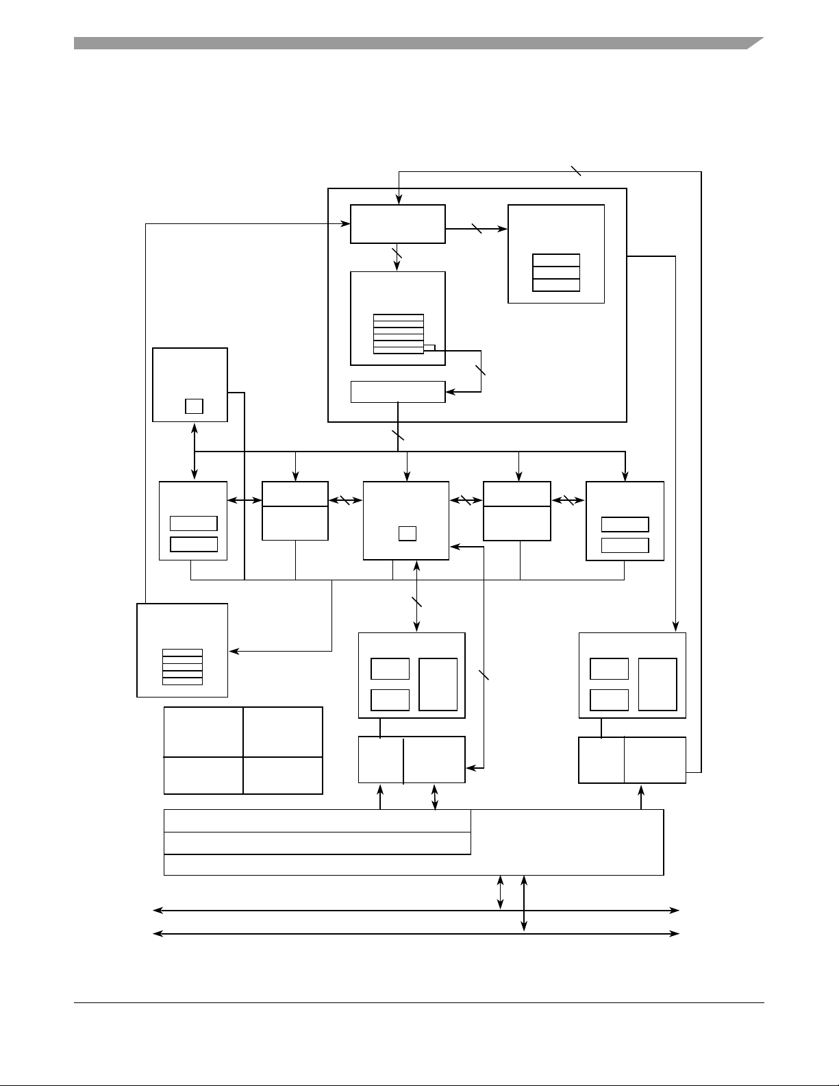
Overview
64-Bit
64-Bit
64-Bit
64-Bit
64-Bit
32-Bit
Branch
Processing
Unit
64-Bit Data Bus
32-Bit Address Bus
Instruction Unit
Integer
Units (2)
Floating-
Point Unit
FPR File
FP Rename
Registers
16-Kbyte
D Cache
Tags
Sequential
Fetcher
CTR
CR
LR
+
*
/
FPSCR
System
Register
Unit
+
*
/
Processor Logic
Bus Interface
D MMU
SRs
DTLB
DBAT
Array
Touch Load Buffer
Copy-Back Bu ffer
Dispatch Unit
64-Bit
Power
Dissipation
Control
Completion
Unit
Time Base
Counter/
Decrementer
Clock
Multiplier
JTAG/COP
Interface
XER
I MMU
SRs
ITLB
IBAT
Array
16-Kbyte
I Cache
Tags
64-Bit32-Bit
GPR File
Load/Store
Unit
+
GP Rename
Registers
Instruction
Queue
+
64-Bit
Figure 1-2 provides a block diagram of the e300 core that shows how the execution units (IU1, IU2, FPU,
BPU, LSU, and SRU) operate independently and in parallel. Note that this is a conceptual diagram that
does not attempt to show how these features are physically implemented on the chip.
Freescale Semiconductor 1-9
Figure 1-2. MPC8308 Integrated e300c3 Core Block Diagram
MPC8308 PowerQUICC II Pro Processor Reference Manual, Rev. 1
Page 74

Overview
1.2.2 DDR2 Memory Controller
This fully programmable DDR2 SDRAM controller supports most JEDEC standard 8 or 16 DDR2
memories available today, including buffered and unbuffered DIMMs. However, mixing non registered
and registered DIMMs in the same system is not supported.
The DDR memory controller includes the following features:
• Support for DDR2 SDRAM
• 16- or 32-bit SDRAM data bus
• Programmable settings for meeting all SDRAM timing parameters
• Many different SDRAM configurations supported
— Support for two physical banks (chip selects)
— Support for 64-Mbit to 1-Gbit devices with 8/16 data ports. Some 2-Gbit devices are
supported depending on the internal device configuration.
— Support for unbuffered and registered DIMMs
• Support for data mask signals and read-modify-write operations for sub-double word writes
• Four-entry input request queue
• Open page management (dedicated entry for each sub-bank)
1.2.3 Dual Enhanced Three-Speed Ethernet Controllers
The MPC8308 has two on-chip enhanced three-speed Ethernet controllers. The eTSECs incorporate a
media access control (MAC) sublayer that supports 10- and 100-Mbps and 1-Gbps Ethernet/IEEE Std.
802.3 networks with MII and RGMII physical interfaces. The eTSECs include 2-Kbyte receive and
10-Kbyte transmit FIFOs and DMA functions. They also support IEEE Std. 1588.
The buffer descriptors are based on the MPC8260 and MPC860T 10/100 Ethernet programming models.
Each eTSEC can emulate a PowerQUICC III TSEC, allowing existing driver software to be re-used with
minimal change.
The MPC8308 eTSECs support programmable CRC generation and checking, RMON statistics, and
jumbo frames of up to 9.6 Kbytes.
Each eTSEC provides hardware support for accelerating TCP/IP packet transmission and reception. By
default, TCP/IP acceleration is not enabled, and the eTSEC processes frames as pure Ethernet frames.
TCP/IP acceleration can be performed at a number of levels. The eTSEC can parse frames at layer 2 of the
stack only (Ethernet headers and switching headers), layers 2 to 3 (including IP v4 or IP v6), or layers 2
to 4 (including TCP and UDP).
On receive, the eTSEC provides protocol header recognition, header verification (IP v4 header checksum
verification), and TCP/UDP payload checksum verification including verification of associated
pseudo-header checksums. On transmit, the eTSEC provides IP v4 and TCP/UDP header checksum
generation. The eTSEC does not checksum transmitted packets with IP header options or IP fragments.
MPC8308 PowerQUICC II Pro Processor Reference Manual, Rev. 1
1-10 Freescale Semiconductor
Page 75

Overview
To provide for quality of service, transmission from up to eight queues is supported with priority-based
queue selection. Arbitration is a modified weighted round-robin queue selection with fair bandwidth
allocation.
On receive, packets may be distributed to any of the 64 virtual receive queues overlaid onto the 8 physical
receive queues. A table-oriented queue filing strategy is provided based on 16 header fields or flags. Frame
rejection is supported for filtering applications.
Filing can be based on Ethernet, IP, and TCP/UDP properties, including VLAN fields, Ether-type, IP
protocol type, IP TOS or differentiated services, IP source and destination addresses, TCP/UDP port
numbers, or user-defined bit fields.
1.2.4 SerDes PHY
The SerDes PHY block includes the SerDes PHY, the protocol converter per protocol, the protocol mux,
and the control registers and control logic.
The SerDes PHY block has the following features:
• Support for one 1 PCI Express interface
• Link-layer interfaces to PCI Express
• Memory-mapped registers with 256-byte address region
• SerDes power-down/reset state machine for cold (power-on) or warm (software-initiated) reset of
SerDes, PHY, and controllers
The SerDes PHY block supports the following mode of operation:
• One lane running 1 PCI Express at 2.5 Gbps
1.2.5 PCI Express Interface
The MPC8308 supports a PCI Express interface compliant with the PCI Express Base Specification
Revision 1.0a. It is able to act as either root complex or endpoint. It only supports virtual channel 0 (VC0)
and eight traffic classes (TC0–TC7). The maximum supported packet payload size is 128 bytes.
The physical layer supports single 1 lane width running at the specified data rate of 2.5 Gbauds.
Inbound INTx transaction is supported and change the state of a level-sensitive interrupt presented to the
PIC. Outbound INTx transaction is supported. Message signaled interrupt (MSI) transaction is supported
and controls up to 256 interrupt sources within the PIC. Outbound MSI transaction may be created by
software using the MSI Capability Register Sets.
The physical layer of the PCI Express interface operates at a 2.5-Gbaud data rate.
1.2.6 Universal Serial Bus (USB) 2.0
The USB 2.0 controller offers operation as a host or device. The USB controller provides point-to-point
connectivity, which complies with the Universal Serial Bus Revision 2.0 Specification. The USB
controllers can be configured to operate as a stand-alone host or stand-alone device. See Figure 1-3 for
more information.
MPC8308 PowerQUICC II Pro Processor Reference Manual, Rev. 1
Freescale Semiconductor 1-11
Page 76

Overview
Dual-Role
CSB
TX Buffer
Module
(DR)
RX Buffer
ULPI
The host and device functions are both configured to support the following four types of USB transfers:
• Bulk
• Control
• Interrupt
• Isochronous
Figure 1-3. USB Controllers Port Configuration
1.2.6.1 USB Dual-Role Controller
• Designed to comply with Universal Serial Bus Revision 2.0 Specification
• Supports operation as a stand-alone USB host controller
— Supports USB root hub with one downstream-facing port
— Enhanced host controller interface (EHCI) compatible
• Supports operation as a stand-alone USB device
— Supports one upstream-facing port
— Supports three programmable bi-directional USB endpoints
• Supports high-speed (480-Mbps), full-speed (12-Mbps), and low-speed (1.5-Mbps) operations.
Low speed is only supported in host mode.
• Host mode direct connect of full-speed and low-speed devices
• Supports USB on-the-go mode when using an external ULPI PHY that includes both device and
host functionality
• Host and device support
1.2.7 Enhanced Local Bus Controller (eLBC)
The main component of the enhanced local bus controller (eLBC) is its memory controller that pro vides a
seamless interface to many types of memory devices and peripherals. The memory controller is
responsible for controlling four memory banks shared by a NAND Flash control machine (FCM), a
general-purpose chip-select machine (GPCM), and up to three user-programmable machines (UPMs). As
MPC8308 PowerQUICC II Pro Processor Reference Manual, Rev. 1
1-12 Freescale Semiconductor
Page 77

Overview
such, it supports a minimal glue logic interface to SRAM, EPROM, NOR Flash EPROM, NAND Flash
EPROM, Flash EPROM, burstable RAM, and other peripherals.
The eLBC also includes a number of data checking and protection features such as data parity generation
and checking, write protection, and a bus monitor to ensure that each bus cycle is terminated within a
user-specified period.
The eLBC provides two Write Enable signals to allow single-byte write access to external 16-bit eLBC
slave devices.
The main features of the enhanced local bus controller (eLBC) are as follows:
• Memory controller with four memory banks (chip selects)
— 32-bit address decoding with mask
— Variable memory block sizes (32 Kbytes to 2 Gbytes in FCM mode, 32 Kbytes to 64 Mbytes
in UPM mode, and 32 Kbytes to 64 Mbytes in GPCM mode)
— Selection of control signal generation on a per-bank basis
— Data buffer controls activated on a per-bank basis
— Up to 256-byte bursts, arbitrarily aligned
— Automatic segmentation of large transactions into memory accesses optimized for bus width
and addressing capability
— Write-protection capability
— Atomic operation
• General-purpose chip-select machine (GPCM)
— Compatible with SRAM, EPROM, NOR Flash EEPROM, FEPROM, and peripherals
— Global (boot) chip-select available at system reset
— Boot chip-select support for 8- and 16-bit devices
— Minimum three-clock access to external devices
— Two byte-write-enable signals (LWE[0:1])
— Output enable signal (LOE)
— External access termination signal (LGTA
)
• NAND Flash control machine (FCM)
— Compatible with small (512 + 16 bytes) and large (2048 + 64 bytes) page parallel NAND
Flash EEPROM
— Global (boot) chip-select available at system reset, with 4-Kbyte boot block buffer for
execute-in-place boot loading
— Boot chip-select support for 8-bit devices
— Dual 2-Kbyte/eight 512-byte buffers allow simultaneous data transfer during Flash reads and
programming
— Interrupt-driven block transfer for reads and writes
— Programmable command and data transfer sequences of up to eight steps supported
— Generic command and address registers support proprietary Flash interfaces
MPC8308 PowerQUICC II Pro Processor Reference Manual, Rev. 1
Freescale Semiconductor 1-13
Page 78

Overview
— Block write locking to ensure system security and integrity
• Three user-programmable machines (UPMs)
— Programmable-array-based machine controls external signal timing with a granularity of up to
one quarter of an external bus clock period
— User-specified control-signal patterns run when an internal master requests a single-beat or
burst read or write access
— UPM refresh timer runs a user-specified control signal pattern to support refresh
— User-specified control-signal patterns can be initiated by software
— Each UPM can be defined to support devices with depths of 64, 128, 256, and 512 Kbytes, and
1, 2, 4, 8, 16, 32, 64 Mbytes
— Support for 8- and 16-bit devices
— Page mode support for successive transfers within a burst
• Optional monitoring of transfers between local bus internal masters and local bus slaves (local bus
error reporting)
1.2.8 Integrated Programmable Interrupt Contro ller (IPIC)
The Integrated Programmable Interrupt Controller (IPIC) implements the necessary functions to provide
a flexible solution for general-purpose interrupt control. The IPIC includes the following features:
• Functional and programming models are compatible with the MPC8260 interrupt controller
• Support for external and internal discrete interrupt sources
• Support for one external (optional) and seven internal machine checkstop interrupt sources
• Programmable highest priority request
• Two programmable priority mixed groups of four on-chip and four external interrupt signals with
two priority schemes for each group: grouped and spread
• Four programmable priority internal groups of eight on-chip interrupt signals with two priority
schemes for each group: grouped and spread
• Priority interrupts can be programmed to support a critical (cint) or system management (smi)
interrupt type
• External and internal interrupts directed to a host processor
• Unique vector number for each interrupt source
• IPIC can support external interrupt request with programmable triggering mechanism. It can be
programmed to use one of the following mechanisms:
— Active low level triggering
— Active high level triggering
— Raising edge triggering
— Falling edge triggering
MPC8308 PowerQUICC II Pro Processor Reference Manual, Rev. 1
1-14 Freescale Semiconductor
Page 79

Overview
1.2.9 I2C Interface
The inter-IC (IIC or I2C) bus is a two-wire—serial data (SDA) and serial clock (SCL)— bidirectional
serial bus that provides a simple, efficient method of data exchange between the system and other devices,
such as microcontrollers, EEPROMs, real-time clock devices, A/D converters, and LCDs. The two-wire
bus minimizes the interconnections between devices. The synchronous, multi-master bus of the I
the connection of additional devices to the bus for expansion and system development.
2
The I
C controller is a true multi-master bus, which includes collision detection and arbitration that
prevents data corruption if two or more masters attempt to control the bus simultaneously. This feature
allows for complex applications with multiprocessor control. The I2C controller consists of a
transmitter/receiver unit, clocking unit, and control unit. The I2C unit supports general broadcast mode and
on-chip filtering rejects spikes on the bus.
The I2C interface includes the following features:
• Two-wire interface
• Multi-master operational
• Arbitration lost interrupt with automatic mode switching from master to slave
• Calling address identification interrupt
• Bus busy detection
• Software-programmable clock frequency
• Software-selectable acknowledge bit
2
C allows
• On-chip filtering for spikes on the bus
• Address broadcasting supported
1.2.10 General Purpose DMA Controller
The direct memory access (DMA) is capable of performing complex data transfers with minimal
intervention from a host processor via two programmable channels. The hardware architecture includes a
DMA engine, which performs source and destination address calculations, and the actual data movement
operations, along with a local memory containing the transfer control descriptors (TCD) for the channels.
This SRAM-based implementation is utilized to minimize the overall module size.
The DMA is a highly programmable data transfer engine that has been optimized to minimize the required
intervention from the host processor. It is intended for use in applications where the data size to be
transferred is statically known, and is not defined within the data packet itself. The DMA hardware
supports:
• Single design with two channels (Tx and Rx)
• 32-byte transfer control descriptor per channel stored in local memory
• 32 bytes of data registers, used as temporary storage to support burst transfers
MPC8308 PowerQUICC II Pro Processor Reference Manual, Rev. 1
Freescale Semiconductor 1-15
Page 80

Overview
1.2.11 Dual Universal Asynchronous Receiver/Transmitter (DUART)
The device includes a Dual universal Asynchronous Reciever/Transmitter (DUART) intended for use in
maintenance, bring up, and debug systems. The device provides a standard two-wire data (TXD and RXD)
for each port. The DUART is a slave interface. An interrupt is provided to the interrupt controller.
Interrupts are generated for transmit, receive, and line status.
The DUART supports full-duplex operation. It is compatible with the PC16450 and PC16550
programming models. The transmitter and receiver both support 16-byte FIFOs.
Software programmable baud rate generators divide the system clock to generate a 16x clock. Serial
interface data formats (data length, parity, 1/1.5/2 STOP bit, baud rate) are also software selectable.
The DUART includes the following features:
• Full-duplex operation
• Programming model compatible with the original PC16450 UART and the PC16550D (an
improved version of the PC16450 that also operates in FIFO mode)
• PC16450 register reset values
• FIFO mode for both transmitter and receiver, providing 16-byte FIFOs
• Serial data encapsulation and decapsulation with standard asynchronous communication bits
(START, STOP, and parity)
• Maskable transmit, receive, and line status interrupts
• Software-programmable baud rate generators that divide the system clock by 1 to (216– 1) and
generate a 16x clock for the transmitter and receiver engines
• Software-selectable serial-interface data format (data length, parity, 1/1.5/2 STOP bit, baud rate)
• Line status registers
• Line-break detection and generation
• Internal diagnostic support, local loopback, and break functions
• Prioritized interrupt reporting
• Overrun, parity, and framing error detection
1.2.12 Enhanced Secure Digital Host Controller (eSDHC)
The enhanced secure digital host controller (eSDHC) provides an interface between the host system and
these types of memory cards:
• MultiMediaCard (MMC)
MMC is a universal low-cost data storage and communication medium designed to cover a wide
area of applications including mobile video and gaming, which are available from either pre-loaded
MMC cards or downloadable from cellular phones, WLAN, or other wireless networks.
• Secure digital (SD) card
The secure digital (SD) card is an evolution of old MMC technology . It is specifically designed to
meet the security, capacity, performance, and environment requirements inherent in the emerging
MPC8308 PowerQUICC II Pro Processor Reference Manual, Rev. 1
1-16 Freescale Semiconductor
Page 81

Overview
audio and video consumer electronic devices. The physical form factor, pin assignments, and data
transfer protocol are forward-compatible with the old MMC.
•SDIO
Under the SD protocol, the SD cards can be categorized as a memory card, I/O card, or combo card.
The memory card invokes a copyright protection mechanism that complies with the security of the
SDMI standard. The I/O card provides high-speed data I/O with low power consumption for
mobile electronic devices. The combo card has both memory and I/O functions.
The eSDHC acts as a bridge, passing host bus transactions to SD/SDIO/MMC cards by sending commands
and performing data accesses to or from the cards. It handles the SD/SDIO/MMC protocol at the
transmission level.
The eSDHC can select the following modes for data transfer:
• SD 1-bit
• SD 4-bit
• MMC 1-bit
• MMC 4-bit
• Identification mode (up to 400 KHz)
• Full-speed mode (up to 25 MHz) or high-speed mode (up to 50 MHz)
1.2.13 System Timers
The system includes the following timers:
• Periodic interrupt timer
• Real time clock
• Software watchdog timer
• One general-purpose timer block, supporting four 16-bit programmable timers or two cascaded
32-bit timers, or one cascaded 64-bit counter
MPC8308 PowerQUICC II Pro Processor Reference Manual, Rev. 1
Freescale Semiconductor 1-17
Page 82

Overview
MPC8308 PowerQUICC II Pro Processor Reference Manual, Rev. 1
1-18 Freescale Semiconductor
Page 83

Chapter 2 Signal Descriptions
This chapter describes the external signals of the device. It is organized into the following sections:
• Overview of signals and cross references for signals that serve multiple functions, including a list
ordered by functional block.
• List of output signal states at reset
NOTE
A bar over a signal name indicates that the signal is active low, such as
MWE. Active-low signals are referred to as asserted (active) when they are
low and negated when they are high. Signals that are not active low , such as
TSEC1_RX_DV (interrupt input), are referred to as asserted when they are
high and negated when they are low.
2.1 Signals Overview
The signals are grouped as follows:
• DDR2 memory interface signals
• DUART interface signals
•I2C interface signals
• Ethernet management interface signals
• eTSEC1 and eTSEC2 interface signals
• PCI Express PHY signals
• Enhanced local bus interface signals
• GPIO interface signals
• Global timers/USB interface signals
Figure 2-1 and Figure 2-2 show the external signals of the device and how the signals are grouped. Refer
to the MPC8308 PowerQUICC II Pro Processor Hardware Specification for a pinout diagram showing
pin numbers and a listing of all the electrical and mechanical specifications.
Note that individual chapters of this document provide details for each signal, describing each signal’s
behavior when asserted and negated and when the signal is an input or an output.
• IPIC interface signals
• SPI interface signals
• JTAG interface signals
• System control signals
• Test interface signals
• Clock interface signals
• eSDHC interface signals
• Miscellaneous signals
• IEEE 1588 signals
MPC8308 PowerQUICC II Pro Processor Reference Manual, Rev. 1
Freescale Semiconductor 2-1
Page 84

Signal Descriptions
MDQ[0:31]
MDQS[0:3]
MBA[2:0]
MA[13:0]
32
4
3
14
MWE
MRAS
MCAS
MCS[0:1]
1
1
1
2
MCKE
1
MCK[0:2]
3
MDM[0:3]
4
MODT[0:1]
2
TSEC1_CRS
TSEC1_RX_CLK
TSEC1_GTX_CLK
1
1
1
TSEC1_TX_CLK/TSEC1_GTX_CLK125
TSEC1_RX_DV
TSEC1_RXD[3:0]
4
1
TSEC1_COL
1
1
1
1
TSEC1_RX_ER
4
TSEC1_TX_EN
TSEC1_TX_ER/LB_POR_CFG_BOOT_ECC
1
TSEC1_TXD[3:0]/CFG_RESET_SOURCE[0:3]
1
1
1
1
1
LGPL0, LFCLE
LCS
[0:3]
LWE0
, LFWE0, LBS0
LBCTL
LGPL1, LFALE
LGPL2, LOE
, LFRE
LGPL3, LFWP
LGPL4, LGTA, LUPWAIT, LFRB
4
1
1
1
DDR2
Memory
Interface
82 Signals
Local Bus
Interface
56 Signals
MPC8308
Enhanced
TSEC1_MDC
TSEC1_MDIO
1
1
Ethernet
Mgmt
Interface
2 Signals
3
MCK
[0:2]
LGPL5
LCLK0
1
eTSEC1
Ethernet
Interface
18 Signals
MECC[0:7]
8
MDM[8]
1
1
MDQS[8]
GPIO/
24 Signals
1
1
1
IRQ
[1]
IRQ
[2]
IRQ
[0]/MCP_IN
1
1
1
1
TCK
TDI
TDO
TMS
TRST
1
IPIC
Interface
4 Signals
JTAG
5 Signals
1
IRQ
[3]/
1
SPIMOSI
SPIMISO
SPICLK
SPISEL
1
1
1
SPI
Interface
4 Signals
LWE1, LBS1
1
/LBC_PM_REF_10
/MCP_OUT
/CKSTOP_OUT
/MSRCID4/LSRCID4
/MDVAL/LDVAL
CKSTOP_IN
/INTA
16
LD[0:15]
26
LA[0:25]
MVREF
1
eTSEC2
GPIO[0]/TSEC2_CRS
GPIO[1]/TSEC2_TX_ER
GPIO[2]/TSEC2_GTX_CLK
GPIO[3]/TSEC2_RX_CLK
GPIO[4]/TSEC2_RX_DV
GPIO[5:7]
GPIO[8]/TSEC2_RXD[0]
GPIO[9]/TSEC2_RX_ER
GPIO[10]/TSEC2_TX_CLK/TSEC2_GTX_CLK125
GPIO[11]/TSEC2_TXD[3]
GPIO[12]/TSEC2_TXD[2]
GPIO[13]/TSEC2_TXD[1]
GPIO[14]/TSEC2_TXD[0]
GPIO[15]/TSEC2_TX_EN
1
1
1
1
1
3
1
1
1
1
1
1
1
1
1
1
1
SD_CLK/GPIO[16]
SD_CMD/GPIO[17]
S
D_CD/GTM1_TIN1/GPIO[18]
SD_WP/GTM1_TGATE1
/GPIO[19]
SD_DAT[0]/GTM1_TOUT1
/GPIO[20]
SD_DAT[1]/GTM1_TOUT2/GPIO[21]
SD_DAT[2]/GTM1_TIN2/GPIO[22]
SD_DAT[3]/GTM1_TGATE2
/GPIO[23]
1
1
1
1
1
GTM1_TGATE3
GTM1_TIN4
GTM1_TGATE
4/GPIO[15]
GTM1_TIN3
1
1
1
1
GTM1_TOUT3/GPIO[9]
GTM1_TOUT
4/GPIO[10]
1
1
1
1
DUART
Interface
4 Signals
1
1
UART_SOUT[1]/MSRCID0/LSRCID0
UART_SOUT[2]/MSRCID2/LSRCID2
UART_SIN[1]/MSRCID1/LSRCID1
UART_SIN[2]/MSRCID3/LSRCID3
eSDHC/
GTM
Interface
14 Signals
TSEC1_GTX_CLK125/TSEC1_TX_CLK
1
GPIO[0]/TSEC2_COL
1
GPIO[5:7]/TSEC2_RXD[3:1]
3
GPIO[1]
GPIO[2]
GPIO[3]
GPIO[4]
1
1
1
1
2-2 Freescale Semiconductor
Figure 2-1. MPC8308 Signal Groupings (1 of 2)
MPC8308 PowerQUICC II Pro Processor Reference Manual, Rev. 1
Page 85

Signal Descriptions
1
1
HRESET
PORESET
MPC8308
1
1
System
Control
3 Signals
Clock
Interface
2 Signals
SYS_CLK_IN
RTC_PIT_CLOCK
THERM0
2 Misc
Signals
1
1
SRESET
1
QUIESCE
TEST_MODE
1
Test
Interface
1 Signal
2
RXA, RXA
SD_IMP_CAL_RX
SD_REF_CLK, SD_REF_CLK
SD_IMP_CAL_TX
2
1
1
PCIExpress
PHY
SD_PLL_TPD
1
SD_PLL_TPA_ANA
1
10 Signals
USBDR_PWR_FAULT
USBDR_CLK
USBDR_DIR
USBDR_NXT
USBDR_TXDRXD[0:7]
USBDR_PCTL[0:1]
USBDR_STP
1
1
1
1
8
2
1
USB
Interface
15 Signals
1
IIC_SCL1
I
2
C
Interface
4 Signals
1
IIC_SDA1
IIC_SCL2/CKSTOP_IN
IIC_SDA2/CKSTOP_OUT
1
1
TSEC_TMR_PP[1:2]
2
TSEC_TMR_ALARM[1]
1
TSEC_TMR_GCLK
1
TSEC_TMR_CLK/GPIO[8]
TSEC_TMR_PP[3]/GPIO[13]
TSEC_TMR_ALARM[2]/GPIO[14]
1
TSEC_TMR_TRIG[1]/GPIO[11]
TSEC_TMR_TRIG[2]/GPIO[12]
1
1
1
1
Interface
IEEE 1588
9 Signals
TXA, TXA
2
Table 2-1 provides a summary of the signals grouped by function. This table details the signal name, its
description, functional block, number of signals, whether the signal is an input, output, or bidirectional
signal, and the alternate functions of the signal. The table also provides a pointer to the table(s) where the
signal function is described.
Name Description
Figure 2-2. MPC8308 Signal Groupings (2 of 2)
Table 2-1. MPC8308 Signal Reference by Functional Block
Functional
Block
No. of
Signals
I/O
Table/
Page
Function(s)
Alternate
MDQ[0:31] DDR data DDR2 32 I/O 9-1/9-4 — —
MECC[0:7] DDR ECC data DDR2 8 I/O 9-1/9-4 — —
MDM[0:3] DDR data mask DDR2 4 O 9-1/9-4 — —
MDM[8] DDR data mask DDR2 1 O 9-1/9-4 — —
MDQS[0:3] DDR data
Freescale Semiconductor 2-3
strobe
MPC8308 PowerQUICC II Pro Processor Reference Manual, Rev. 1
DDR2 4 I/O 9-1/9-4 — —
Table/
Page
Page 86

Signal Descriptions
Table 2-1. MPC8308 Signal Reference by Functional Block (continued)
Name Description
MDQS[8] DDR data
Functional
Block
DDR2 1 I/O 9-1/9-4 — —
No. of
Signals
I/O
Table/
Page
Alternate
Function(s)
Table/
Page
strobe
MBA[2:0] DDR bank
DDR2 3 O 9-1/9-4 — —
select
MA[13:0] DDR address DDR2 14 O 9-1/9-4 — —
MWE DDR write
DDR2 1 O 9-1/9-4 — —
enable
MRAS DDR row
DDR2 1 O 9-1/9-4 — —
address strobe
MCAS DDR column
DDR2 1 O 9-1/9-4 — —
address strobe
MCS[0:1] DDR chip
DDR2 2 O 9-1/9-4 — —
select
(2/DIMM)
MCKE DDR clock
DDR2 1 O 9-1/9-4 — —
enable
MCK[0:2] DDR differential
DDR2 3 O 9-1/9-4 — —
clocks
MCK[0:2] DDR differential
clocks
MODT[0:1] DRAM on-die
termination
MVREF DDR2 DRAM
reference
TSEC1_COL eTSEC1
collision detect
TSEC1_CRS eTSEC 1 carrier
sense
TSEC1_GTX_CLK eTSEC1
transmit clock
out
TSEC1_RX_CLK eTSEC1
receive clock
TSEC1_RX_DV eTSEC1
receive data
valid
TSEC1_RXD[3:0] eTSEC1
receive
data 3–0
DDR2 3 O 9-1/9-4 — —
DDR2 2 O 9-1/9-4 — —
DDR2 1 PWR 9-1/9-4 — —
eTSEC1 1 I 16-2/16-7 — —
eTSEC1 1 I 16-2/16-7 — —
eTSEC1 1 O 16-2/16-7 — —
eTSEC1 1 I 16-2/16-7 — —
eTSEC1 1 I 16-2/16-7 — —
eTSEC1 4 I 16-2/16-7 — —
TSEC1_RX_ER eTSEC1
eTSEC1 1 I 16-2/16-7 — —
receiver error
MPC8308 PowerQUICC II Pro Processor Reference Manual, Rev. 1
2-4 Freescale Semiconductor
Page 87

Table 2-1. MPC8308 Signal Reference by Functional Block (continued)
Signal Descriptions
Name Description
TSEC1_TX_CLK eTSEC1
transmit clock in
TSEC1_TXD[3:0] eTSEC1
transmit
data 3–0
TSEC1_TX_EN eTSEC1
transmit enable
TSEC1_TX_ER eTSEC1
transmit error
TSEC1_GTX_CLK125 Gigabit
reference cloc k
TSEC2_COL eTSEC2
collision detect
TSEC2_TX_ER eTSEC2
transmit error
TSEC2_GTX_CLK eTSEC2
transmit clock
out
TSEC2_RX_CLK eTSEC2
receive clock
Functional
Block
eTSEC1 1 I 16-2/16-7 TSEC1_GTX_
No. of
Signals
I/O
Table/
Page
Alternate
Function(s)
Table/
Page
16-2/16-7
CLK125
eTSEC1 4 I/O 16-2/16-7 CFG_RESET_
4-1/4-1
SOURCE[0:3]
eTSEC1 1 O 16-2/16-7 LBC_PM_REF_10 —
eTSEC1 1 I/O 16-2/16-7 LB_POR_CFG_
—
BOOT_ECC
eTSEC1 1 I 16-2/16-7 TSEC1_TX_CLK 16-2/16-7
eTSEC2 1 I 16-2/16-7 GPIO[0] 21-1/21-2
eTSEC2 1 O 16-2/16-7 GPIO[1] 21-1/21-2
eTSEC2 1 O 16-2/16-7 GPIO[2] 21-1/21-2
eTSEC2 1 I 16-2/16-7 GPIO[3] 21-1/21-2
TSEC2_RX_DV eTSEC2
receive data
valid
TSEC2_RXD[3:1] eTSEC2
receive
data 3–1
TSEC2_RXD[0] eTSEC2
receive
data 0
TSEC2_RX_ER eTSEC2
receiver error
TSEC2_TX_CLK eTSEC2
transmit clock in
TSEC2_GTX_CLK125 Gigabit
reference cloc k
TSEC2_TXD[3:0] eTSEC2
transmit
data 3–0
TSEC2_TX_EN eTSEC2
transmit enable
eTSEC2 1 I 16-2/16-7 GPIO[4] 21-1/21-2
eTSEC2 3 I 16-2/16-7 GPIO[5:7] 21-1/21-2
eTSEC2 1 I 16-2/16-7 GPIO[8] 21-1/21-2
eTSEC2 1 I 16-2/16-7 GPIO[9] 21-1/21-2
eTSEC2 1 I 16-2/16-7 GPIO[10]/
21-1/21-2/
TSEC2_GTX_CLK125
eTSEC2 1 I 16-2/16-7 GPIO[10]/
21-1/21-2/
TSEC2_TX_CLK
eTSEC2 4 O 16-2/16-7 GPIO[11:14] 21-1/21-2
eTSEC2 1 O 16-2/16-7 GPIO[15] 21-1/21-2
MPC8308 PowerQUICC II Pro Processor Reference Manual, Rev. 1
Freescale Semiconductor 2-5
Page 88

Signal Descriptions
Table 2-1. MPC8308 Signal Reference by Functional Block (continued)
Name Description
TSEC2_CRS eTSEC 2 carrier
sense
GPIO[0] General-purpos
e I/O signal
GPIO[0] General-purpos
e I/O signal
GPIO[1] General-purpos
e I/O signal
GPIO[2] General-purpos
e I/O signal
GPIO[3] General-purpos
e I/O signal
GPIO[4] General-purpos
e I/O signal
GPIO[1] General-purpos
e I/O signal
GPIO[2] General-purpos
e I/O signal
Functional
Block
No. of
Signals
I/O
Table/
Page
Alternate
Function(s)
Table/
Page
eTSEC2 1 I 16-2/16-7 GPIO[0] 21-1/21-2
GPIO 1 I/O 21-1/21-2 TSEC2_COL 16-2/16-7
GPIO 1 I/O 21-1/21-2 TSEC2_CRS 16-2/16-7
GPIO 1 I/O 21-1/21-2 TSEC2_TX_ER 16-2/16-7
GPIO 1 I/O 21-1/21-2 TSEC2_GTX_CLK 16-2/16-7
GPIO 1 I/O 21-1/21-2 TSEC2_RX_CLK 16-2/16-7
GPIO 1 I/O 21-1/21-2 TSEC2_RX_DV 16-2/16-7
GPIO 1 I/O 21-1/21-2
— —
GPIO 1 I/O 21-1/21-2
— —
GPIO[3] General-purpos
e I/O signal
GPIO[4] General-purpos
e I/O signal
GPIO[5:7] General-purpos
e I/O signal
GPIO[5:7] General-purpos
e I/O signal
GPIO[8] General-purpos
e I/O signal
GPIO[8] General-purpos
e I/O signal
GPIO[9] General-purpos
e I/O signal
GPIO[10] General-purpos
e I/O signal
GPIO[9:10] General-purpos
e I/O signal
GPIO[11:12] General-purpos
e I/O signal
GPIO 1 I/O 21-1/21-2
— —
GPIO 1 I/O 21-1/21-2
— —
GPIO 3 I/O 21-1/21-2 — —
GPIO 3 I/O 21-1/21-2 TSEC2_RXD[3:1] 16-2/16-7
GPIO 1 I/O 21-1/21-2 TSEC2_RXD[0] 16-2/16-7
GPIO 1 I/O 21-1/21-2 TSEC_TMR_CLK 16-2/16-7
GPIO 1 I/O 21-1/21-2 TSEC2_RX_ER 16-2/16-7
GPIO 1 I/O 21-1/21-2 TSEC2_TX_CLK/
16-2/16-7
TSEC2_GTX_CLK125
GPIO 2 I/O 21-1/21-2 GTM1_TOUT[3:4] 5-53/5-56
GPIO 2 I/O 21-1/21-2 TSEC_TMR_TRIG[1:2] 16-2/16-7
GPIO[13] General-purpos
GPIO 1 I/O 21-1/21-2 TSEC_TMR_PP[3] 16-2/16-7
e I/O signal
MPC8308 PowerQUICC II Pro Processor Reference Manual, Rev. 1
2-6 Freescale Semiconductor
Page 89

Table 2-1. MPC8308 Signal Reference by Functional Block (continued)
Signal Descriptions
Name Description
GPIO[14] General-purpos
Functional
Block
GPIO 1 I/O 21-1/21-2 TSEC_TMR_ALARM[2] 16-2/16-7
No. of
Signals
I/O
Table/
Page
Alternate
Function(s)
Table/
Page
e I/O signal
GPIO[11:14] General-purpos
GPIO 4 I/O 21-1/21-2 TSEC2_TXD[3:0] 16-2/16-7
e I/O signal
GPIO[15] General-purpos
GPIO 1 I/O 21-1/21-2 TSEC2_TX_EN 16-2/16-7
e I/O signal
GPIO[15] General-purpos
GPIO 1 I/O 21-1/21-2 GTM1_TGATE4 5-53/5-56
e I/O signal
TSEC_TMR_GCLK 1588 clock-out eTSEC 1 O 16-2/16-7 — —
TSEC_TMR_CLK 1588 clock-in eTSEC 1 I 16-2/16-7 GPIO[8] 21-1/21-2
TSEC_TMR_PP[1:2] 1588 timer
eTSEC 2 O 16-2/16-7 — —
pulse-out 1, 2
TSEC_TMR_PP[3] 1588 timer
eTSEC 1 O 16-2/16-7 GPIO[13] 21-1/21-2
pulse-out 3
TSEC_TMR_
ALARM[1]
TSEC_TMR_
ALARM[2]
1588 timer
alarm-out 1
1588 timer
alarm-out 2
eTSEC 1 O 16-2/16-7 — —
eTSEC 1 O 16-2/16-7 GPIO[14] 21-1/21-2
TSEC_TMR_TRIG[1:2]1588 trigger-in
eTSEC 2 I 16-2/16-7 GPIO[11:12] 21-1/21-2
1, 2
USBDR_PWR_FAULT USB VBus
USB 1 I 13-2/13-3 — —
power faul t
USBDR_CLK Clocking signal
USB 1 I 13-2/13-3 — —
for ULPI PHY
interface
USBDR_DIR Direction of
USB 1 I 13-2/13-3 — —
data bus
USBDR_NXT Nest data USB 1 I 13-2/13-3 — —
USBDR_TXDRXD[0:7] Data bit 0–7 USB 8 I/O 13-2/13-3 — —
USBDR_PCTL[0:1] Port control 0–1 USB 2 O 13-2/13-3 — —
USBDR_STP End of a
USB 1 O 13-2/13-3 — —
transfer on the
bus
TSEC1_MDC Ethernet
management
Ethernet
Management
1 O 16-2/16-7 — —
data clock
TSEC1_MDIO Ethernet
management
Ethernet
Management
1 I/O 16-2/16-7 — —
data in/out
MPC8308 PowerQUICC II Pro Processor Reference Manual, Rev. 1
Freescale Semiconductor 2-7
Page 90

Signal Descriptions
Table 2-1. MPC8308 Signal Reference by Functional Block (continued)
Name Description
CFG_RESET_
SOURCE[0:3]
Reset
configuration
Functional
Block
Reset and
clock
word source
selection
CKSTOP_IN Checkstop in Reset and
clock
CKSTOP_IN Checkstop in Reset and
clock
CKSTOP_OUT Checkstop out Reset and
clock
CKSTOP_OUT Checkstop out Reset and
clock
TXA Serial
transmitter,
PCI Express
PHY
lane A, positive
data
TXA Serial
transmitter,
PCI Express
PHY
lane A, negative
data
(complement)
No. of
Signals
I/O
Table/
Page
Alternate
Function(s)
4 I 4-1/4-1 TSEC1_TXD[3:0] 16-2/16-7
1 I — IRQ3/INTA 8-1/8-5
1 I — IIC_SCL2 17-1/17-3
1 O — IRQ2 8-1/8-5
1 O — IIC_SDA2 17-1/17-3
1 O 15-1/15-2 — —
1 O 15-1/15-2 — —
Table/
Page
RXA Serial receiver,
lane A, positive
data
RXA Serial receiver,
lane A, negative
data
(complement)
SD_IMP_CAL_RX Receiver
impedance
control signal
SD_REF_CLK SerDes PLL
reference cloc k
SD_REF_CLK SerDes PLL
reference cloc k
(complement)
SD_PLL_TPD Digital test point
for SerDes PLL
testing
SD_IMP_CAL_TX Transmitter
impedance
control signal
PCI Express
PHY
PCI Express
PHY
PCI Express
PHY
PCI Express
PHY
PCI Express
PHY
PCI Express
PHY
PCI Express
PHY
1 I 15-1/15-2 — —
1 I 15-1/15-2 — —
1 I 15-1/15-2 — —
1 I 15-1/15-2 — —
1 I 15-1/15-2 — —
1 O — — —
1 I 15-1/15-2 — —
MPC8308 PowerQUICC II Pro Processor Reference Manual, Rev. 1
2-8 Freescale Semiconductor
Page 91

Table 2-1. MPC8308 Signal Reference by Functional Block (continued)
Signal Descriptions
Name Description
XCOREVDD[0:2] SerDes
transceiver core
supply
XCOREVSS[0:2] SerDes
transceiver core
ground
XPADVDD[0:1] SerDes
transceiver pad
supply
XPADVSS[0:1] SerDes
transceiver pad
ground
SDAVDD Analog supply
for SerDes PLL
SD_PLL_TPA_ANA Analog test
point for
SerDes PLL
testing
SDAVSS Analog ground
for SerDes PLL
Functional
Block
PCI Express
PHY
PCI Express
PHY
PCI Express
PHY
PCI Express
PHY
PCI Express
PHY
PCI Express
PHY
PCI Express
PHY
No. of
Signals
I/O
Table/
Page
Alternate
Function(s)
3 PWR — — —
3 GND — — —
2 PWR — — —
2 GND — — —
1 PWR — — —
1 O — — —
1 GND — — —
Table/
Page
LB_POR_CFG_
BOOT_ECC
Enable/Disable
ECC for Flash
eLBC 1 I — TSEC1_TX_ER 16-2/16-7
during RCW
load
LBC_PM_REF_10 Status of
eLBC 1 O — TSEC1_TX_EN 16-2/16-7
uncorrectable
ECC error in
FCM during
boot loading
from Flash
LD[0:15] LBC data eLBC 16 I/O 10-2/10-5 — —
LA[0:25] LBC port
eLBC 26 O 10-2/10-5 — —
address
LCS[0:3] LBC chip select
eLBC 4 O 10-2/10-5 — —
0–3
LWE0, LFWE0, LBS0 LBC write
eLBC 1 O 10-2/10-5 — —
enable, Byte
(lane) select
LWE1, LBS1 LBC write
eLBC 1 O 10-2/10-5 — —
enable, Byte
(lane) select
LBCTL LBC data buffer
eLBC 1 O 10-2/10-5 — —
control
MPC8308 PowerQUICC II Pro Processor Reference Manual, Rev. 1
Freescale Semiconductor 2-9
Page 92

Signal Descriptions
Table 2-1. MPC8308 Signal Reference by Functional Block (continued)
Name Description
LGPL0, LFCLE LBC UPM
general
purpose line 0,
Flash
command latch
enable
LGPL1, LFALE LBC GP line 1,
Flash address
latch enable
LGPL2, LOE, LFRE LBC GP line 2,
LBC output
enable, Flash
read enable
LGPL3, LFWP LBC GP line 3,
Flash write
protect
LGPL4, LGTA,
LUPWAIT, LFRB
LBC GP line 4,
Transaction
termination,
External device
wait, Flash
ready/busy
Functional
Block
No. of
Signals
I/O
Table/
Page
Alternate
Function(s)
eLBC 1 O 10-2/10-5 — —
eLBC 1 O 10-2/10-5 — —
eLBC 1 O 10-2/10-5 — —
eLBC 1 O 10-2/10-5 — —
eLBC 1 I/O 10-2/10-5 — —
Table/
Page
LGPL5 LBC GP line 5 eLBC 1 O 10-2/10-5 — —
LCLK0 LBC clock eLBC 1 O 10-2/10-5 — —
IIC_SDA1 I2C serial data 1 I2C 1 I/O 17-1/17-3 — —
IIC_SDA2 I2C serial data 2 I2C 1 I/O 17-1/17-3 CKSTOP_OUT —
IIC_SCL1 I2C serial clock
I2C 1 I/O 17-1/17-3 — —
1
IIC_SCL2 I2C serial clock
I2C 1 I/O 17-1/17-3 CKSTOP_IN —
2
UART_SOUT[1] DUART serial
data out
UART_SOUT[2] DUART serial
data out
UART_SIN[1] DUART serial
data in
UART_SIN[2] DUART serial
data in
SPIMOSI SPI master-out
slave-in
SPIMISO SPI master-in
slave-out
DUART 1 O 18-1/18-3 MSRCID0/LSRCID0 —,
10-2/10-5
DUART 1 O 18-1/18-3 MSRCID2/LSRCID2 —,
10-2/10-5
DUART 1 I/O 18-1/18-3 MSRCID1/LSRCID1 —,
10-2/10-5
DUART 1 I/O 18-1/18-3 MSRCID3/LSRCID3 —,
10-2/10-5
SPI 1 I/O 19-1/19-6 MSRCID4/LSRCID4 —,
10-2/10-5
SPI 1 I/O 19-1/19-6 MDVAL/LDVAL —,
10-2/10-5
MPC8308 PowerQUICC II Pro Processor Reference Manual, Rev. 1
2-10 Freescale Semiconductor
Page 93

Table 2-1. MPC8308 Signal Reference by Functional Block (continued)
Signal Descriptions
Name Description
Functional
Block
No. of
Signals
I/O
Table/
Page
Alternate
Function(s)
Table/
Page
SPICLK SPI clock SPI 1 I/O 19-1/19-6 — —
SPISEL SPI slave select SPI 1 I 19-1/19-6 — —
IRQ[0] External
IPIC 1 I 8-1/8-5 MCP_IN —
interrupt 0
IRQ[1] External
IPIC 1 I/O 8-1/8-5 MCP_OUT 8-1/8-5
interrupt 1
IRQ[2] External
IPIC 1 I/O 8-1/8-5 CKSTOP_OUT —
interrupt 2
IRQ[3] External
interrupt 3
INTA Interrupt
request output
MCP_IN Machine check
IPIC 1 I 8-1/8-5 CKSTOP_IN, INTA —,
8-1/8-5
IPIC 1 O 8-1/8-5 CKSTOP_IN, IRQ3 —,
8-1/8-5
IPIC 1 I — IRQ[0] 8-1/8-5
interrupt input
MCP_OUT Machine check
IPIC 1 O 8-1/8-5 IRQ[1] 8-1/8-5
interrupt output
TCK Test clock JTAG 1 I 20-1/20-2 — —
TDI Test data in JTAG 1 I 20-1/20-2 — —
TDO Test data out JTAG 1 O 20-1/20-2 — —
TMS Test mode
JTAG 1 I 20-1/20-2 — —
select
TRST Test reset JTAG 1 I 20-1/20-2 — —
TEST_MODE Internal test
Test 1 I — — —
signal
Note: "This pin
must always be
tied to VSS"
PORESET Power on reset System
1 I 4-1/4-1 — —
control
HRESET Hard reset System
1 I/O 4-1/4-1 — —
control
SRESET Soft reset System
1 I/O 4-1/4-1 — —
control
SYS_CLK_IN Clock input Clocks 1 I 4-2/4-2 — —
RTC_PIT_CLOCK 32.768 KHz
Clocks 1 I 15-1/15-4 — —
clock input to
RTC
AVDD1 Core PLL
Misc 1 PWR — — —
power supply
MPC8308 PowerQUICC II Pro Processor Reference Manual, Rev. 1
Freescale Semiconductor 2-11
Page 94

Signal Descriptions
Table 2-1. MPC8308 Signal Reference by Functional Block (continued)
Name Description
AVDD2 System PLL
Functional
Block
Misc 1 PWR — — —
No. of
Signals
I/O
Table/
Page
Alternate
Function(s)
Table/
Page
power supply
QUIESCE Quiescent state Misc 1 O 5-64/5-70 — —
THERM0 Thermal
Misc 1 I — — —
resistor access
0
SD_CLK eSDHC clock
eSDHC 1 O 11-1/11-5 GPIO[16] 21-1/21-2
out
SD_CMD eSDHC
eSDHC 1 I/O 11-1/11-5 GPIO[17] 21-1/21-2
command/
response
signals
SD_CD Card detection
signal
SD_WP Write protection
signal
SD_DAT[0] Data signal 0 eSDHC 1 I/O 11-1/11-5 GTM1_TOUT1/
SD_DAT[1] Data signal 1 eSDHC 1 I/O 11-1/11-5 GTM1_TOUT2/
eSDHC 1 I 11-1/11-5 GTM1_TIN1/
GPIO[18]
eSDHC 1 I 11-1/11-5 GTM1_TGATE1/
GPIO[19]
GPIO[20]
GPIO[21]
5-53/5-56/
21-1/21-2
5-53/5-56/
21-1/21-2
5-53/5-56/
21-1/21-2
5-53/5-56/
21-1/21-2
SD_DAT[2] Data signal 2 eSDHC 1 I/O 11-1/11-5 GTM1_TIN2/
GPIO[22]
SD_DAT[3] Data signal 3 eSDHC 1 I/O 11-1/11-5 GTM1_TGATE2/
GPIO[23]
GTM1_TIN1 Timer in 1 Global
1 I 5-53/5-56 SD_CD/GPIO[18] 11-1/11-5/
Timers
GTM1_TGATE1 Timer gate 1 Global
1 I 5-53/5-56 SD_WP/GPIO[19] 11-1/11-5/
Timers
GTM1_TOUT1 Timer out 1 Global
1 O 5-53/5-56 SD_DAT[0]/GPIO[20] 11-1/11-5/
Timers
GTM1_TIN2 Timer in 2 Global
1 I 5-53/5-56 SD_DAT[2]/GPIO[22] 11-1/11-5/
Timers
GTM1_TGATE2 Timer gate 2 Global
1 I 5-53/5-56 SD_DAT[3]/GPIO[23] 11-1/11-5/
Timers
GTM1_TOUT2 Timer out 2 Global
1 O 5-53/5-56 SD_DAT[1]/GPIO[21] 11-1/11-5/
Timers
GTM1_TIN3 Timer in 3 Global
1 I 5-53/5-56 — —
Timers
GTM1_TGATE3 Timer gate 3 Global
1 I 5-53/5-56 — —
Timers
5-53/5-56/
21-1/21-2
5-53/5-56/
21-1/21-2
21-1/21-2
21-1/21-2
21-1/21-2
21-1/21-2
21-1/21-2
21-1/21-2
MPC8308 PowerQUICC II Pro Processor Reference Manual, Rev. 1
2-12 Freescale Semiconductor
Page 95

Table 2-1. MPC8308 Signal Reference by Functional Block (continued)
Signal Descriptions
Name Description
GTM1_TOUT[3:4] Timer out 3, 4 Global
GTM1_TIN4 Timer in 4 Global
GTM1_TGATE4 Timer gate 4 Global
MSRCID0/LSRCID0 Memory debug
source ID
MSRCID1/LSRCID1 Memory debug
source ID
MSRCID2/LSRCID2 Memory debug
source ID
MSRCID3/LSRCID3 Memory debug
source ID
MSRCID4/LSRCID4 Memory debug
source ID
MDVAL/LD VAL Memory debug
data valid
Functional
Block
Timers
Timers
Timers
Debug 1 O —,
Debug 1 O —,
Debug 1 O —,
Debug 1 O —,
Debug 1 O —,
Debug 1 O —,
No. of
Signals
I/O
2 I/O 5-53/5-56 GPIO[9:10] 21-1/21-2
1 I 5-53/5-56 — —
1 I 5-53/5-56 GPIO[15] 21-1/21-2
Table/
Page
10-2/10-5
10-2/10-5
10-2/10-5
10-2/10-5
10-2/10-5
10-2/10-5
Alternate
Function(s)
UART_SOUT[1] 18-1/18-3
UART_SIN[1] 18-1/18-3
UART_SOUT[2] 18-1/18-3
UART_SIN[2] 18-1/18-3
SPIMOSI 19-1/19-6
SPIMISO 19-1/19-6
Table/
Page
2.2 Output Signal States During Reset
When a system reset is recognized (PORESET or HRESET are asserted), the device aborts all current
internal and external transactions (with the exception of RTC) and releases all bidirectional I/O signals to
a high-impedance state. See Chapter 4, “Reset, Clocking, and Initialization,” for a complete description of
the reset functionality.
During reset, the device ignores most input signals (except for the reset configuration signals) and drives
most of the output-only signals to an inactive state. Table 2-2 shows the states of the output-only signals.
Table 2-2. Output Signal States During System Reset
Interface Signal State During Reset
MDM[0:3] DDR data mask High-Z
MDM[8] DDR data mask High-Z
MBA[2:0] DDR bank select High-Z
MA[13:0] DDR address High-Z
MWE
MRAS
MCAS DDR column address strobe High-Z
MCS[0:1] DDR chip select (2/DIMM) High-Z
DDR write enable High-Z
DDR row address strobe High-Z
MPC8308 PowerQUICC II Pro Processor Reference Manual, Rev. 1
Freescale Semiconductor 2-13
Page 96

Signal Descriptions
UART_SOUT[1:2] DUART serial data out High-Z
Table 2-2. Output Signal States During System Reset (continued)
Interface Signal State During Reset
MCKE DDR clock enable Driven Low
MCK[0:2] DDR differential clocks Low
[0:2] DDR differential clocks Low
MCK
MODT[0:1] DRAM on-die termination Driven Low
LA[0:25] LBC port address Active—used to load reset configuration
word
LCS[0] LBC chip select 0 Active—used to load reset configuration
word
LCS[1:3] LBC chip select High
LWE[0:1] LBC write enable High
LBCTL LBC data buffer control Active—used to load reset configuration
word
/LGPL2 LBC output enable/GP line 2 Active—used to load reset configuration
LOE
word
LCLK0 LBC clock 0 High-Z
LGPL[0:1], LGPL[3:5] LBC UPM General purpose line High
TSEC1_MDC Ethernet management data clock Low
TSEC1_GTX_CLK eTSEC1 transmit clock out Low
TSEC1_TXD[3:0] eTSEC1 transmit data 3–0 Low
TSEC1_TX_EN eTSEC1 transmit enable Low
TSEC1_TX_ER eTSEC1 transmit error Low
TSEC2_TXD[3:0] eTSEC2 transmit data 3–0 Low
TSEC2_TX_EN eTSEC2 transmit enable Low
TSEC2_TX_ER eTSEC2 transmit error Low
TSEC_TMR_GCLK 1588 clock-out Low
TSEC_TMR_PP[1:3] 1588 timer pulse-out 1, 2, 3 Low
TSEC_TMR_ALARM[1:2] 1588 timer alarm-out 1, 2 Low
SD_CLK eSDHC clock out Low
SD_PLL_TPD Digital test point for SerDes PLL testing High
TDO Test data out High-Z
QUIESCE
Quiescent state High
GTM1_TOUT[3:4] Timer out 3, 4 High
MPC8308 PowerQUICC II Pro Processor Reference Manual, Rev. 1
2-14 Freescale Semiconductor
Page 97

Table 2-2. Output Signal States During System Reset (continued)
Interface Signal State During Reset
USBDR_PCTL[0:1] Port control 0–1 Low
USBDR_STP End of a transfer on the bus High
Signal Descriptions
MPC8308 PowerQUICC II Pro Processor Reference Manual, Rev. 1
Freescale Semiconductor 2-15
Page 98

Signal Descriptions
MPC8308 PowerQUICC II Pro Processor Reference Manual, Rev. 1
2-16 Freescale Semiconductor
Page 99

Chapter 3 Memory Map
This chapter describes the MPC8308 memory map. The internal memory-mapped registers are described,
including a complete listing of all memory-mapped registers with cross references to the sections detailing
descriptions of each.
3.1 Internal Memory-Mapped Registers
All of the memory-mapped registers in the device are contained within a 1-Mbyte address region. T o allow
for flexibility , the base address of the memo ry-mapped registers is re-locatable in the local address space.
The local address map location of this register block is controlled by the internal memory-mapped registers
base address register (IMMRBAR). See Section 5.1.4.1, “Internal Memory Map Registers Base Address
Register (IMMRBAR),” for more information. The default value for IMMRBAR is 0xFF40_0000.
3.2 Accessing IMMR Memory from the Local Processor
When the local e300 processor is used to configure IMMR space, the IMMR memory space should
typically be marked as cache-inhibited and guarded.
In addition, many configuration registers affect accesses to other memory regions; therefore, writes to
these registers must be guaranteed to have taken effect before accesses are made to the associated memory
regions.
To guarantee that the results of any sequence of writes to configuration registers are in effect, the final
configuration register write should be followed immediately by a read of the same register, and that should
be followed by a sync instruction. Then accesses can safely be made to memory regions affected by the
configuration register write.
3.3 IMMR Address Map
Table 3-1 lists the location of the functional block base addresses for the entire IMMRBAR space. Unless
stated otherwise in a particular block, all accesses to and from the memory-mapped registers must be made
with 32-bit accesses. There is no support for accesses of sizes other than 32 bits.
Reading from address locations that appear as reserved in the memory map table is not guaranteed to return
predictable data. Writing to address locations that appear as reserved in the memory map table is not
allowed and could lead to unpredictable behavior of the device. Reserved bits in non-reserved registers are
read as zero unless the reset value of those bits is different due to internal logic considerations.
When writing to registers with reserved bits, those reserved bits should be cleared. By doing so, existing
software would be able to run on a future modified device in which some reserved bits were allocated for
enhanced modes. This would allow for maintaining the legacy functionality when set to zero.
MPC8308 PowerQUICC II Pro Processor Reference Manual, Rev. 1
Freescale Semiconductor 3-1
Page 100

Memory Map
In certain specific cases, reserved bits should not be cleared but should keep their reset value. Thus, the
software should perform a ‘read-modify-write’ and make sure that it does not change the reset value of
those bits. The description of the specific bits indicate when this is needed.
Cross-references are provided to the IMMRBAR maps for each individual block. A complete listing of all
registers is provided in Appendix A, “Complete List of Configuration, Control, and Status Registers.”
Table 3-1. IMMR Memory Map
Block Base Address Block Actual Size Window
0x0_0000–0x0_01FF System configuration 512 bytes 512 bytes 5.2.1/5-15
0x0_0200–0x0_02FF Watchdog timer 16 bytes 256 bytes 5.3.4/5-34
0x0_0300–0x0_03FF Real time clock 32 bytes 256 bytes 15.6/15-5
0x0_0400–0x0_04FF Periodic interval timer 32 bytes 256 bytes 5.5.5/5-49
0x0_0500–0x0_05FF Global timers module 64 bytes 256 bytes 5.6.5/5-57
0x0_0600–0x0_06FF Reserved — 256 bytes —
0x0_0700–0x0_07FF Integrated programmable
interrupt controller (IPIC)
0x0_0800–0x0_08FF System arbiter 30 bytes 256 bytes 6.2/6-2
0x0_0900–0x0_09FF Reset module 44 bytes 256 bytes 4.5.1/4-25
0x0_0A00–0x0_0AFF Clock module 44 bytes 256 bytes 4.5.2/4-29
0x0_0B00–0x0_0BFF Power management control
module
0x0_0C00–0x0_0CFF GPIO 24 bytes 256 bytes 21.3/21-2
0x0_0D00–0x0_1FFF Reserved — 4.8 Kbytes —
0x0_2000–0x0_2FFF DDR2 memory controller 3.8 Kbytes 4 Kbytes 9.4/9-9
2
0x0_3000–0x0_30FF I
0x0_3100–0x0_31FF I
C controller 1 24 bytes 256 bytes
2
C controller 2 24 bytes 256 bytes
128 bytes 256 bytes
20 bytes 256 bytes 5.7.2/5-70
Section/
Page
8.5/8-6
17.3/17-4
0x0_3200–0x0_44FF Reserved — 4.8 Kbytes —
0x0_4500–0x0_46FF DUART (UAR T1 and U AR T2) 18 bytes 24Kbytes18.3/18-3
0x0_4700–0x0_4FFF Reserved — 2.3 Kbytes —
0x0_5000–0x0_5FFF eLBC 224 bytes 4 Kbytes 10.3/10-7
0x0_6000–0x0_6FFF Reserved — 4 Kbytes —
0x0_7000–0x0_7FFF SPI 24 bytes 4 Kbytes 19.3/19-7
0x0_8000–0x0_8FFF Reserved — 4 Kbytes —
0x0_9000–0x0_9FFF PCI Express 4 Kbytes 4 Kbytes 14.3/14-5
0x0_A000–0x2_2FFF Reserved 4 Kbytes 102.4 Kbytes —
0x2_3000–0x2_3FFF USB dual-role (DR) controller 4 Kbytes 4 Kbytes
MPC8308 PowerQUICC II Pro Processor Reference Manual, Rev. 1
3-2 Freescale Semiconductor
13.3/13-4
 Loading...