

Page 1

nc...
, I
or
Freescale Semiconductor, Inc.
3/1999
Rev 1.0
MPC8260 PowerQUICC II
emiconduct
eescale S
Fr
MPC8260-TCOM User’s Manual
MOTOROLA
For More Information On This Product,
Go to: www.freescale.com
Page 2

MPC8260TCOM User’s Manual PRELIMINARY
0•1 INTRODUCTION
This page provides unpacking instructions, hardware preparation, and installation instructions for the
MPC8260TCOM.
0•2 UNPACKING INSTRUCTIONS
If the shipping carton is damaged upon receipt,
request carrier’s agent be present during
unpacking and inspection of equipment.
Unpack equipment from shipping carton. Refer to packing list and verify that all items are present. Save
packing material for storing and reshipping of equipment.
Freescale Semiconductor, Inc.
nc...
, I
or
AVOID TOUCHING AREAS OF INTEGRATED
CIRCUITRY; STATIC DISCHARGE CAN
DAMAGE CIRCUITS.
NOTE
CAUTION
emiconduct
eescale S
Fr
2
For More Information On This Product,
Go to: www.freescale.com
Page 3

nc...
, I
or
emiconduct
PRELIMINARY MPC8260TCOM User’s Manual
Freescale Semiconductor, Inc.
GENERAL INFORMATION
CHAPTER 1 - GENERAL INFORMATION
1•1 INTRODUCTION
This manual provides general information, preparation for use and installation instructions, operating
instructions, functional description, and support information for the MPC8260TCOM board.
1•2 FEATURES
The main features of the MPC8260TCOM board are as follows:
• Two Fast Ethernet channels connected guilelessly to the Level One LXT970 device.
• The 2 Fast-Ethernet use FCC1 and FCC3.
• Each one of the Fast - Ethernet module can be disable/disable and controlled by SW.
• Two DS3 channels using the TRAN-SWITCH TXC-03401 FRAMER and TRAN-SWITCH TXC20153G DS3 Line Interface Module.
• Each one of the DS3 framer controlled via the MPC8260.
• The 2XDS3 use the TDMA1(DS3_1 FCC2) and TDMA2 (DS3_2 FCC3).
• Each one of the DS3 module can be disable/enable by HW.
• Eight T1 interfaces using MCC1 and MCC2.
• The 8 x T1 use the TOCTL PM4388 as a framer and 2 x PM4314 as a line interface module, both
controlled by the MPC8260.
• Each one of the eight T1 can be independently configured, monitor, isolated and controlled by
SW.
• The TOCTL (PM4388) is controlled by the MPC8260 via the address and data bus.
• The MPC8260TCOM board is powered and controlled by the MPC8260ADS via 2 x 128pin DIN
connectors.
1•3 SPECIFICATIONS
The MPC8260TCOM specifications are given in Table 1-1.
Table 1-1 MPC860SAR-PHY Specifications
eescale S
Fr
Power requirements (no other boards attached) +5Vdc @ 2 A (typical), 2.5 A (maximum)
Operating temperature 0 degrees to 30 degrees C ambient air temperature
Storage temperature -25 degrees to 85 degrees C
Relative humidity 5% to 90% (non-condensing)
Dimensions
Height
Depth
Thickness
CHARACTERISTICS SPECIFICATIONS
9.17 inches (233 mm)
6.3 inches (160 mm)
0.063 inches (1.6 mm)
For More Information On This Product,
Go to: www.freescale.com
3
Page 4

MPC8260TCOM User’s Manual PRELIMINARY
GENERAL INFORMATION
1•4 GENERAL DESCRIPTION
The MPC8260TCOM Board includes the following modules: 8 x T1/E1, 2 x Fast Ethernet, 2 x DS3.
The MPC8260ADS includes the following modules: ATM155 and Fast Ethernet.
Both MPC8260TCOM and MPC8260ADS implements the following network for H/W & S/W development
applications:
ATM155M (FCC1 on MPC8260ADS) + 8 x T1 (MCC1 & MCC2),
ATM155M (FCC1 on MPC8260ADS) + 2 x Fast Ethernet (FCC2 on MPC8260ADS, FCC3),
ATM155M (FCC1 on MPC8260ADS) + 2 x DS3 (TDMa1 to FCC2, TDMa2 to FCC3),
3 x Fast Ethernet (FCC2 on MPC8260ADS, FCC1, FCC3).
NOTE: Some modules share the same GPIO. Care must be taken when configuring each one of the
modules, to prevent a conflict between them. Before operating the board the user should define the modes
of operation and configure the MPC8260 GPIO to the corresponding module.
nc...
, I
Special care must be taken when using the Fast Ethernet interfaces. It do not have a h/w enable
signal, it is configured only through the MII MDC,MDIO signals.
Freescale Semiconductor, Inc.
or
emiconduct
eescale S
Fr
4
For More Information On This Product,
Go to: www.freescale.com
Page 5

PRELIMINARY MPC8260TCOM User’s Manual
Freescale Semiconductor, Inc.
GENERAL INFORMATION
1•5 RELATED DOCUMENTATION
The following publications are applicable to the MPC8260TCOM and may provide additional helpful
information.
• MPC8260 Spec.
• MPC-SIERRA TOCTL PM4388. (http://www.pmc-sierra.com/register/toctl.asp#D)
• MPC-SIERRA QDSX PM4314. (http://www.pmc-sierra.com/register/qdsx.asp#D)
• Level-One LXT970 Fast - Ethernet Transceiver. (http://www.level1.com/product/qa/
lxt970qa.html)
• TRAN-SWITCH TXC-03401 DS3 FRAMER. (http://www.transwitch.com/pdh.html#ds3f)
• TRANS-SWITCH TXC20153G DS3 Line Interface Module. (http://www.transwitch.com/
pdh.html#limsn)
nc...
• TRANS-SWITCH TXC020020 DS3 Line Interface Device. (http://www.transwitch.com/pdh.html#)
, I
or
emiconduct
eescale S
Fr
1•6 ABBREVIATIONS USED IN THE DOCUMENT
• FCC - Fast serial Communication Controller.
• MCC - Multi Channel Controller.
• FE - Fast Ethernet.
• TOCTL - PMC-Sierra framer PM4388.
• LIU - Line interface module.
• QDSX - PMC-sierra LIU PM4314.
• DS3 - Serial communication of 44.736Mbps.
• DS3F - DS3 Framer.
• TCOM - MPC8260TCOM Board
• GPIO - General Purpose I/O related to the MPC8260 PORTS.
• ADS - MPC8260ADS
• Module - Each one of the options this board can give: 8 x T1, 2 x FE, 2 x DS3.
• CPM - Communication Processor Module.
• SPEC - Engineering Specification document.
1•7 REQUIRED EQUIPMENT
The MPC8260TCOM operates only with the MPC8260ADS.
The equipment required to connect the communication lines to the two cards is described bellow:
• The RJ45 connectors are separated to two groups:
• 8 x E1/T1 circuit connected by a 8 wires cable.
• 2 x Fast Ethernet circuit connected by a 8 wires cable.
• 4 x BNC 75Ω dedicated to 2 x DS3 circuit connected by a BNC cable. (2 - receive, 2 - transmit)
For More Information On This Product,
Go to: www.freescale.com
5
Page 6

MPC8260TCOM User’s Manual PRELIMINARY
GENERAL INFORMATION
Freescale Semiconductor, Inc.
FIGURE 1-1 MPC8260TCOM Connections.
nc...
, I
or
emiconduct
eescale S
Fr
6
For More Information On This Product,
Go to: www.freescale.com
Page 7

PRELIMINARY MPC8260TCOM User’s Manual
Freescale Semiconductor, Inc.
SOFTWARE AND HARDWARE PREPARATION
CHAPTER 2 - SOFTWARE AND HARDWARE PREPARATION
2•1 SOFTWARE PREPARATION
The TCOM is not a stand alone board. It should be connected to the MPC8260ADS. To select the desired
configuration and ensure proper operation of the MPC8260TCOM board, changes in the MPC8260 GPIO
configuration may be required. The following table describes the different configurations of all the modules
on the board.
NOTE:
The FEmoduleshavenoH/Wprotection.BeforeusingoneoftheFEmodulemakesurethatothermodules
using the same GPIO are disabled. The following table shows the various types of communication
channels that can be implemented by connecting the TCOM & ADS cards.
The I/O are related to the MPC8260.
The dark column are the modules on the ADS.
nc...
, I
or
emiconduct
eescale S
Fr
Table 2: Ports Function Signals
TDM1
T1
T1
T1
T1
T1
T1
T1
1
2
3
4
5
Ports/name
PA2/DS3-TXCLK/TDMD2-TXCLK(clock20) I I
PA6/DS3-RXSYNC/TDMA1-L1RSYNC I
PA7/DS3-TXSYNC/TDMA1-L1TSYNC I
PA8/DS3-RXD0/TDMA1-L1RXD0 I
PA9/DS3-TXD0/TDMA1-L1TXD0 O
PA14/MIIRXD3/ATM8-RXD4
PA15//MIIRXD2/ATM8-RXD5 II
PA16/MIIRXD1/ATM8-RXD6 II
PA17/MIIRXD0/ATM8-RXD7 II
PA18/MIITXD0/ATM8-TXD7 OO
PA19/MIITXD1/ATM8-TXD6 OO
PA20/MIITXD2/ATM8-TXD5 OO
PA21/MIITXD3/ATM8--TXD4 OO
PA26/MIIRXER/ATM8-RxClav II
PA27/MIIRXDV/ATM8-RxSOC II
PA28/MIITXEN/ATM8-RxEnb OO
PA29/MIITXER/ATM8-TxSOC OO
PA3/DS3-RXD1/TDMD2-RXCLK(clock19) I I
PA30/MIICRS/ATM8-TxClav
PA31/MIICOL/ATM8-TxEnb OI
PB4/MIITXD3/DS3-RXSYNC/TDMA2-L1RSYNC I O I
PB5/MIITXD2/DS3-TXSYNC//TDMA2-L1TSYNC
PB6/MIITXD1/DS3-RXD0/TDMA2-L1RXD0 I
PB7/MIITXD0/DS3-TXD0/TDMA2-L1TXD0 O
PB8/MIIRXD0/TDMD1-L1RSYNC I
PB9/MIIRXD1/DS3-TXD2/TDMD1-L1TSYNC I
PB10/MIIRXD2/TDMD1-L1RXD I
PB11/MIIRXD3/TDMD1-L1TXD O
PB12/MIICRS/TDMC1-L1RSYNC I
PB13/MIICOL/DS3-TXD1/TDMC1-L1TSYNC I
PB14/MIITXEN/TDMC1-L1RXD I
PB15/MIITXER/TDMC1-L1TXD O
PB16/MIIRXER
A1
B1
C1
D1
6
A2
B2
I O I
C2
T1
7
8
D2
FE
ADS
1
ATM8
FCC1
II
II
ADS
FE
FE 0
2
FCC2
FCC3
OI
OO
I
IO
I
I
I
IO
O
O
I
DS3
FCC2
O
TDM2
1
I
I
I
DS3
FCC3
2
For More Information On This Product,
Go to: www.freescale.com
7
Page 8

MPC8260TCOM User’s Manual PRELIMINARY
Freescale Semiconductor, Inc.
SOFTWARE AND HARDWARE PREPARATION
Table 2: Ports Function Signals
T1
T1
T1
T1
T1
T1
T1
1
2
3
4
5
Ports/name
PB17/MIIRXDV I
PB18/DS3-RXD2/MIIRXD3
PB19/DS3-RXD3/MIIRXD2
PB20/DS3-TXD1/TDMD2-L1RSYNC/MIIRXD1 I
PB21/DS3-TXD2/TDMD2-L1TSYNC/MIIRXD0 I
PB22/DS3-RXD1/TDMD2-L1RXD/MIITXD0 I
PB23/DS3-RXD2/TDMD2-L1TXD/MIITXD1 O
PB24/DS3-RXD3/TDMC2-L1RSYNC/MIITXD2 I
PB25/DS3-TXD3/TDMC2-L1TSYNC/MIITXD3 I
PB26/TDMC2-L1RXD/MIICRS I
PB27/TDMC2-L1TXD/MIICOL O
PB28/TDMB2-L1TSYNC/MIIRXER I
PB29/TDMB2-L1RSYNC/MIITXEN I
PB30/TDMB2-L1RXD/ATM8-MIIRXDV I
PB31/TDMB2-L1TXD/MIITXER O
nc...
PC9/MIIMDIO
PC10/MIIMDC
, I
PC11/DS3-TXD3
or
PC16/MIITXCLK(clock16)/TDMB2-TXCLK I
PC17/MIIRXCLK(clock15)/TDMB2-RXCLK I
PC18/TDMA2-TXCLK(clock14)/MIITXCLK I
PC19TDMA2-/RXCLK(clock13)/MIIRXCLK I
PC20/MIITXCLK(clock12)/ATM8-TxClk
PC21/MIIRXCLK(clock11)/ATM8-RxClk II
PC22/TDMB1-TXCLK(clock10) I
PC23/TDMB1-RXCLK(clock9) I
PC24/TDMD1-TXCLK(clock8) I
PC25/TDMD1-RXCLK(clock7) I
PC26/DS3-TXCLK(clock6)/TDMC1-L1TXCLK(clock6) I I
emiconduct
PC27/DS3-RXCLK(clock5)/TDMC1-L1RXCLK(clock5) I
PC28/TDMC2-TXCLK(clock4) I
PC29/TDMC2-RXCLK(clock3) I
PC30//TDMA1-TXCLK(clock2) I
PC31/DS3-RXCLK(clock1)/TDMA1-RXCLK(clock1) I I
PD10/TDMB1-L1RSYNC I
PD11/TDMB1-L1TSYNC I
PD12/TDMB1-L1RXD I
PD13/TDMB1-L1TXD O
eescale S
A1
B1
C1
D1
A2
6
B2
C2
T1
7
8
D2
FE
ADS
1
ATM8
FCC1
X X X
X X X
II
ADS
FE
FE 0
2
FCC2
FCC3
II
II
IO
IO
OI
OI
OI
OO
I
I
I
O
I
O
I
I
I
I
TDM1
DS3
1
FCC2
TDM2
DS3
2
FCC3
O
I
Fr
8
For More Information On This Product,
Go to: www.freescale.com
Page 9

nc...
, I
or
PRELIMINARY MPC8260TCOM User’s Manual
Freescale Semiconductor, Inc.
SOFTWARE AND HARDWARE PREPARATION
2•1•1 Module Selection.
2•1•1•1 Fast Ethernet selection
As mentioned above, the FE is enabled/disabled by S/W using PC9, PC10 as MII: MDIO and MDC pins.
The FE control is done via the MII internal registers.
FE_1 address = 00001h
FE_2 address = 00010h.
FE_0 address = 00000h (ADS).
2•1•1•2 8 x T1/E1
Each one of the 8 x T1/E1 is enabled by the following ports:
PD4 - T1_1
PD5 - T1_2
PD6 - T1_3
PD7 - T1_4
PD8 - T1_5
PD9 - T1_6
PD18 - T1_7
PD19 - T1_8
emiconduct
eescale S
Fr
2•1•1•3 2 x DS3
Each one of the 2 x DS3 is enabled/disabled by the following ports:
PD25 - DS3 _1 (DS3_1 is enabled only if T1_1 & T1_7 & T1_8 is disabled and PD25 is low).
PA4 - DS3 _2 (DS3_2 is enabled only if T1_3 & T1_4 &T1_5 & T1_8 is disabled and PA4 is low).
2•2 INDICATORS
The MPC8260TCOM has the following indicators.
2•2•1 Fast Ethernet 1 TXD. LD1
LD1 is light whenever the MPC8260 transmits data to FE_1 (LXT970 - U1).
2•2•2 Fast Ethernet 1 RXD. LD2
LD2 is light whenever the MPC8260 receives data from FE_1 (LXT970 - U1).
2•2•3 Fast Ethernet 2 TXD. LD3
LD3 is light whenever the MPC8260 transmits data to FE_2 (LXT970 - U2).
2•2•4 Fast Ethernet 2 RXD. LD4
LD4 is light whenever the MPC8260 receives data from FE_2 (LXT970 - U2).
2•2•5 Fast Ethernet 1 SPEED. LD5
LD5 is light whenever FE_1 (LXT970 - U1) is configured to Fast Ethernet.
For More Information On This Product,
Go to: www.freescale.com
9
Page 10

MPC8260TCOM User’s Manual PRELIMINARY
SOFTWARE AND HARDWARE PREPARATION
Freescale Semiconductor, Inc.
2•2•6 Fast Ethernet 1 LINK/LOCK. LD6
LD6 indicates in 100Mbps a scrambler lock and receipt of valid idle code.
LD6 indicates in 10Mbps a Link Valid status.
2•2•7 Fast Ethernet 1 Collision. LD7
LD7 indicates in default mode a collision.
LXT970 can be programmed for other indications. For detailed description see the LXT970 user’s manual.
2•2•8 Fast Ethernet 2 SPEED. LD8
LD8 is light whenever the FE_2 (LXT970 - U1) is configured to Fast Ethernet.
2•2•9 Fast Ethernet 2 LINK/LOCK. LD9
LD9 indicates in 100Mbps a scrambler lock and receipt of valid idle code. (LXT970 - U2)
LD9 indicates in 10Mbps a Link Valid status.
2•2•10 Fast Ethernet 2 Collision. LD10
nc...
, I
or
emiconduct
eescale S
Fr
LD10 indicates in default mode a collision.
LXT970 can be programmed for other indications.
2•2•11 DS3 2 FRAME ERROR. LD11
LD11 is light whenever an error on the F-bit or M-bit is occurred.
2•2•12 DS3 2 RXLOS. LD12
LD12 is light whenever 175 ± 75 consecutive zeros appear in incoming data stream.
2•2•13 DS3 2 ENABLE. LD13
LD13 is light whenever DS3 2 is enabled.
2•2•14 DS3 1 FRAME ERROR. LD14
LD14 is light whenever an error on the F-bit or M-bit is occurred.
2•2•15 DS3 1 RXLOS LD15
LD15 is light whenever 175 ± 75 consecutive zeros appear in incoming data stream.
2•2•16 DS3 1 ENABLE. LD16
LD16 is light whenever DS3 2 is enabled.
2•2•17 T1/E1 8 ENABLE. LD17
LD17 is light whenever T1/E1 _8 is enabled.
2•2•18 T1/E1 7 ENABLE. LD18
LD18 is light whenever T1/E1_7 is enabled.
2•2•19 T1/E1 6 ENABLE. LD19
LD19 is light whenever T1/E1_6 is enabled.
2•2•20 T1/E1 5 ENABLE. LD20
LD20 is light whenever T1/E1_5 is enabled.
10
For More Information On This Product,
Go to: www.freescale.com
Page 11

PRELIMINARY MPC8260TCOM User’s Manual
2•2•21 T1/E1 4 ENABLE. LD21
LD21 is light whenever T1/E1_4 is enabled.
2•2•22 T1/E1 3 ENABLE. LD22
LD22 is light whenever T1/E1_3 is enabled.
2•2•23 T1/E1 2 ENABLE. LD23
LD23 is light whenever T1/E1_2 is enabled.
2•2•24 T1/E1 1 ENABLE. LD24
LD24 is light whenever T1/E1_1 is enabled.
Freescale Semiconductor, Inc.
SOFTWARE AND HARDWARE PREPARATION
nc...
, I
or
emiconduct
eescale S
Fr
For More Information On This Product,
Go to: www.freescale.com
11
Page 12

MPC8260TCOM User’s Manual PRELIMINARY
SOFTWARE AND HARDWARE PREPARATION
FE_1 FE_2
DS3_2
Freescale Semiconductor, Inc.
FIGURE 1-2 MPC8260TCOM Board
nc...
, I
Fast Ethernet
or
emiconduct
eescale S
Fr
T1_8 T1_7 T1_6 T1_5 T1_4 T1_3 T1_2 T1_1
DS3_1
DS3
T1
12
For More Information On This Product,
Go to: www.freescale.com
Page 13

PRELIMINARY MPC8260TCOM User’s Manual
Freescale Semiconductor, Inc.
FUNCTIONAL DESCRIPTION
CHAPTER 3 - FUNCTIONAL DESCRIPTION
3•1 INTRODUCTION
This chapter details the hardware design of the MPC8260TCOM, and describes each module.
3•2 GENERAL DESCRIPTION
The MPC8260TCOM includes four parts.
• 1. M8260ADS include the MPC8260 device on board.
• 2. Fast Ethernet include the LXT970 devices.
• 3. DS3 include the TXC-03401 framer and 20153G line interface module.
• 4. T1 include the TOCTL framer PM4388 and PM4314 line interface.
The following paragraphs will show the TCOM block diagram and describe each one of the board parts.
nc...
FIGURE 4-1 8260TCOM BLOCK DIAGRAM
, I
or
emiconduct
eescale S
Fr
PMC TOCTL
8X FRAMER 3.3V
5v friendly
transformer
8XT1
RJ45
COC
PMC
LIU
X4
PMC
LIU
X4
8
BNC
CON
DS3
MCC
CONT
LOGIC
2
FRAMER
TRAN
SWITCH
TXC-03401
DS3
T3- LINE
INTERFACE
MODULE
TXC-20153D
BNC
CON
MCC
ADS-CONNECTORS
FRAMER
TRAN
SWITCH
TXC-03401
T3- LINE
INTERFACE
MODULE
TXC-20153D
BNC
CON
FCC3
FCC2
data/address/Io/cont
F-Ethernet
LEVL-ONE
LXT970
MII 3v output
2XFAST ETHERNET
HALO
TG22-3506ND
Transformer
RJ45
CON
BNC
CON
5v 3v
FCC1
IN
LINE
IN
LINE
OUT
LINE
OUT
LINE
For More Information On This Product,
Go to: www.freescale.com
13
Page 14

MPC8260TCOM User’s Manual PRELIMINARY
FUNCTIONAL DESCRIPTION
Freescale Semiconductor, Inc.
3•3 CONTROL LOGIC BLOCK
MACH
nc...
, I
or
emiconduct
eescale S
Fr
FE
rst
QDSX
rst
FE
CS/ADD
CSQDSX1
to 8260
2xDS3ENrec
TOCTL
CSTOCTL
T1 signals X 8
ADD/DATA
RESET
2
QDSX
T1 Buffers
CSQDSX2
ALE(GPL0)
READ WRITE (GPL2 GPL3)
8GPIOIN
ENDS3_1
ENDS3_2
GPIO
8
Enable Signals
DIRDATA
CSDS3F1
DS3F DS3F
REC
BUF
to 8260
LIU
LIU
LINE
Transmit
REC
BUF
to 8260
CSDS3F2
LIU
LIU
LINE
Transmit
MII
to 8260
14
MII
to 8260
to 8260
to 8260
8 GPIO
from 8260
For More Information On This Product,
Go to: www.freescale.com
Data Buff
DIRDATA(GPL4)
Add Buff
AddEN(GPL1)
Page 15

nc...
, I
or
PRELIMINARY MPC8260TCOM User’s Manual
Freescale Semiconductor, Inc.
FUNCTIONAL DESCRIPTION
3•4 MPC8260ADS
The MPC8260ADS is meant to serve as a platform for S/W and H/W development around the MPC8260.
Using its on board resources and its associated debugger, a developer is able to load his code, run it, set
breakpoints, display memory and registers and connect his own proprietary H/W via the CPM expansion
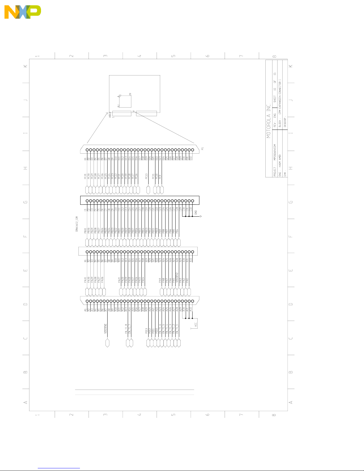
connectors (P1 and P2 on the MPC8260TCOM), to be incorporated to a desired system with the MPC8260
device.
3•5 Ethernet. - 100BASE-TX and 10BASE-T
Two Fast-Ethernet modules used FCC1 (FE_1) and FCC3 (FE_2) are on this board, together with the Fast
Ethernet on the ADS board it will be possible to run 3 Fast Ethernet modules at the same time or it is
possible to disable each one of them to let the user to use the FCC’s for other uses. The disable can be
done by the MDIO bus. The device that use to perform the transceiver operation is the Level One LXT970.
The LXT970 is an IEEE 802.3 compliant 10/100Mbps Fast Ethernet PHY Transceiver that directly supports
both 100BASE-TX and 10BASE-T applications. Provides a Media Independent Interface (MII) for easy
attachment to 10/100 Media Access Controller (MAC)s. The LXT970 supports full-duplex operation at 10
and 100 Mbps. Its operating condition can be set using autonegotiation panel detection or manual control.
The configuration of the LXT970 can be controlled via the MII serial port (MDIO Interface). This interface
allows upper-layer devices to control or monitor the LXT970. The LXT970 can also be controlled via
external pin settings (Hardware Control Interface). This option is not supported on the 8260TCOM.
The LXT970 is connected to the MPC8260 via the FCC1 and FCC3 that performs MII interface through
the I/O ports.
emiconduct
eescale S
Fr
3•6 DS3 (T3).
Two DS3 modules are on this board; they use the TDMA1 (FCC2) and TDMA2 (FCC3). Each one of the
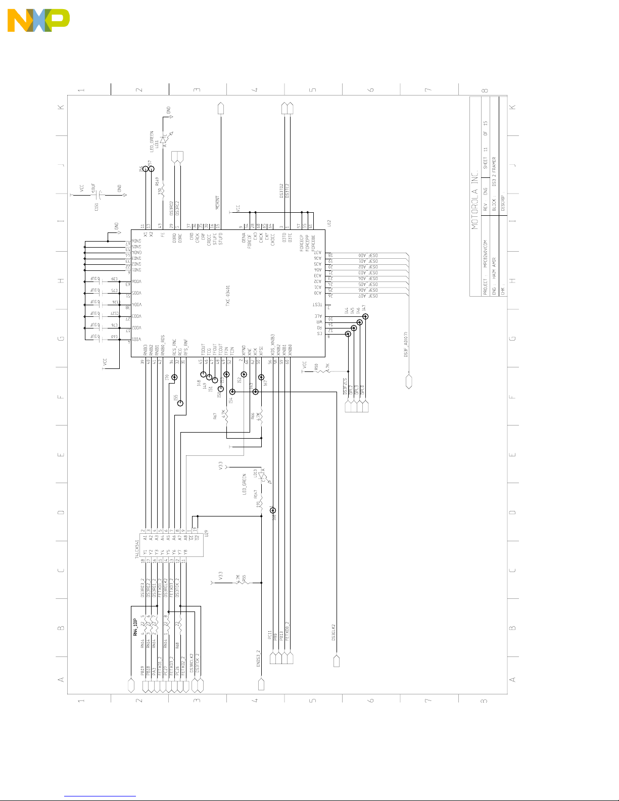
DS3 module is composed of Framer and Line Interface Unit. The DS3 Framer is TRAN-SWITCH TXC-
03401. It is a 5V device. The MPC8260 device is a 3.3V device. That is why a 5V to 3.3V translator is
needed in the output direction from the framer, to bridge between the DS3F, (5V) to the MPC8260 (3.3V)
The device used is a 74LXT541.
The DS3F is designed for DS3 framer applications in which broadband payloads are mapped into the
44.736 Mbit/s DS3 frame format. The payload interface is nibble-parallel format.
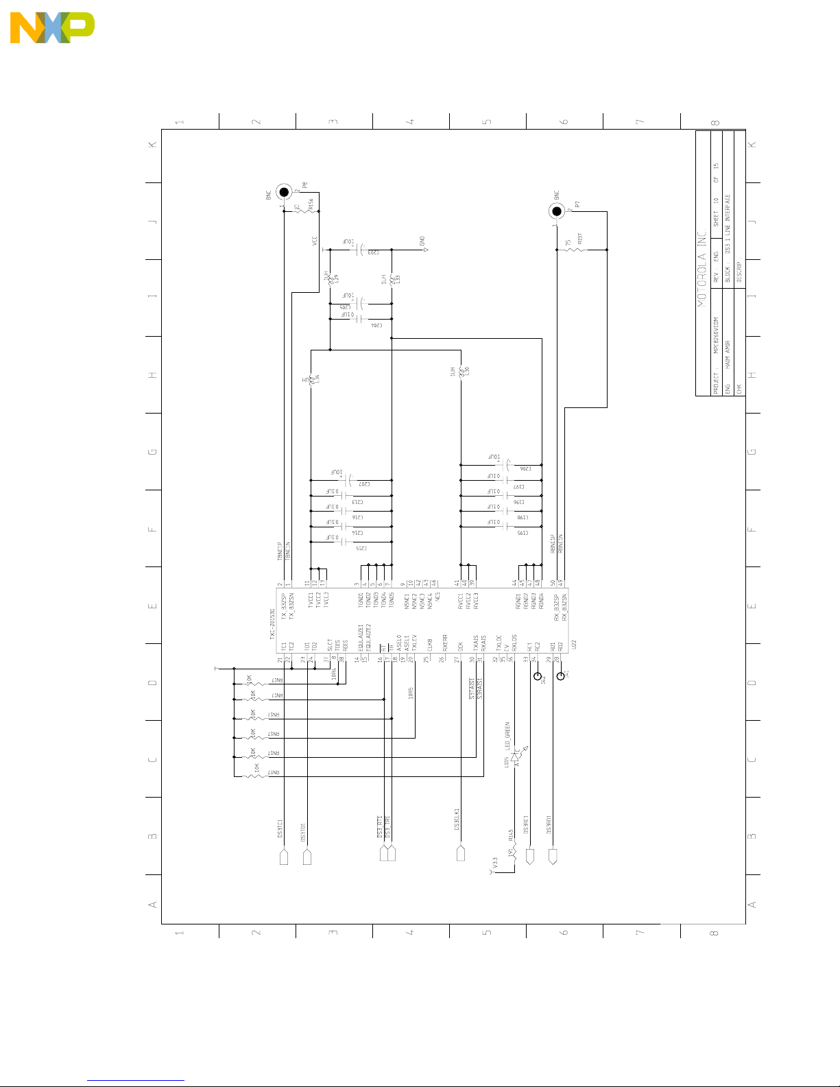
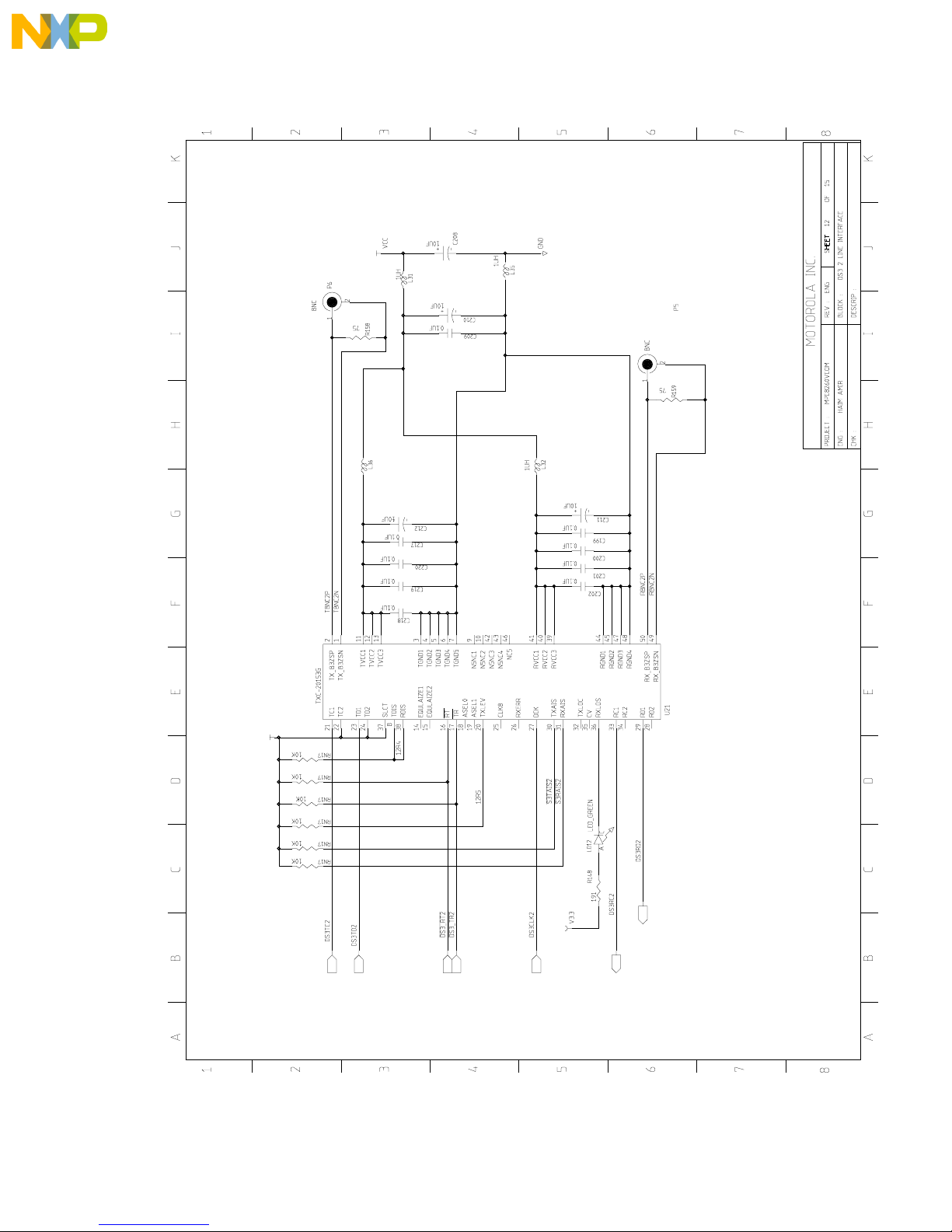
The Line Interface Unit is a TRAN-SWITCH TXC-20153G, this LIU is a module which include the
transformer and the TRAN SWITCH TXC-02020 LIU device. It connected from one side to the DS3F and
from the other side to BNC connector. It is a 5V device.
Each one of the DS3 module can be isolated by a logic control to let the user to use FCC2 and FCC3 for
other purposes.
The DS3 Line Interface Module (DS3LIM-SN) is a complete and compact full duplex analog line to digital
terminal interface. It converts B3ZS - encoded line signals, in either DS3 asynchronous, to and from NRZ
data and clock signals, in addition to the synchronous signal option.
In order to enable DS3_1, PD4 (T1_1) & PD18 (T1_7) & PD19 (T1_8) should be high -’1’ and then drive
PD25 to be low -’0’. In order to enable DS3_2, PD6 (T1_3) & PD7 (T1_4) & PD8 (T1_5) & PD19 (T1_8)
should be high -’1’ and then drive PA4 to be low -’0’. Each one of the DS3 module has a led to light when
this DS3 module is enable, LD13 for DS3_2 and LD16 for DS3_1. Each DS3 modules also has a Frame
Error and Receive signal loss leds.
Each one of the DS3 module have two loopback capabilities for testing transmit and receive loopback via
the loopback controls block of the TXC-20153G.
Transmit - to - Receive loopback connects the data path from the transmit I/O control block output to the
receive I/O control block input, and disable the external receiver input.
Transmit - to - Receive loopback is activated by placing a low on the TR signal pin.
Receive - to Transmit loopback connects the receive data output path to the transmit input circuits and
disable the NRZ transmit input.
For More Information On This Product,
Go to: www.freescale.com
15
Page 16

MPC8260TCOM User’s Manual PRELIMINARY
FUNCTIONAL DESCRIPTION
Receive - to - transmit loopback activated by placing a low on RT pin.
For more information see the TXC-20153G and TXC-02020 user manual.
The physical control to the RT, TR signals of both DS3 modules are controlled as follow:
DS3_1 RT will be low if PA5 and PA1 will be low. (if PA1 is high there is no loop back at all)
DS3_1 TR will be low if PA5 will be high and PA1 will be low. (if PA1 is high there is no loop back at all)
DS3_2 RT will be low if PC13 and PA1 will be low. (if PA1 is high there is no loop back at all)
DS3_2 TR will be low if PC13 will be high and PA1 will be low. (if PA1 is high there is no loop back at all)
Freescale Semiconductor, Inc.
3•7 T1
The T1 is a 1.544Mhz serial line; this board can handle up to 8 T1 line simultaneously. All the T1 modules
on this board are composed by one PM4388 (Framer), 2 PM4314 (LIU) and 2 ST5170 transformers. The
PM4388 device includes 8 T1 framers, each framer in this device can be controlled by its own internal
registers. The PM4388 controlled by the MPC8260 data and address bus. It gets its chip select signal from
the control logic. The PM4314, which is a quad line interface unit, is connected from one side to the framer,
PM4388, and from the other side to the line transformer. Each one of the T1 line interface units can be also
nc...
, I
or
emiconduct
eescale S
Fr
controlled by the internal registers. This device is also connected to the MPC8260 by the address and data
bus. It gets it’s chip select signal from the control logic. The ST5170 includes a 4 transformers, each one
of the ST5170 connected to one PM4314 device.
Each one of the MPC8260 T1 group of signals can be isolate from the framer by buffer. (The PM4388
device can not isolate independently one of the eight T1 signal group). T1_1,2,3,4 modules can be isolated
by PD4-PD7. ’0’ on these signals enables each T1 interface. The T1-5,6,7,8 modules can be isolated by
PD8, PD9, PD18 and PD19. ’0’ on these signals enables each T1 interface. 8 leds are placed on the board
to show which one of the T1 port is enable. Each led lights depend upon the enable T1 signal, for example
if PD4 will be low LD24 (T1_1 enable) will light.
Together with the 8260ADS board it will be possible to operate the8xT1andATM155Mbps or Fast
Ethernet over FCC1.
3•8 Control Logic.
The control logic allows the user to disable each one of the following elements: 8 x T1, 2 x DS3 and 4 x
DS3 loopback options. Although each one of the T1 is enabled directly from the MPC8260, all the T1
enable signals insert to the logic control, in order to disable a DS3 module that share some signal(s) as
T1_x. If one of the T1 enable and it share the same signals as one of the DS3, the appropriate DS3 will be
disable.
Each one of the Fast-Ethernet modules connected to FCC1,FCC2 and FCC3 (on the 8260TCOM or on the
8260ADS) is controlled via the MDIO and MDC signals (PC10, PC9); the SW should be aware that
enabling the Fast Ethernet without disabling the corresponding element that share the same GPIO signals
will damage the board. FE1 share the signals as the ATM module on the ADS, FE0 (the one that is placed
on the 8260ADS) share some of the T1_8, T1_7, T1_6 and T1_5. FE2 share some of the signals of T1_6,
T1_5, T1_4 T1_3
In order to use DS3 the SW should drive PD25 for DS3_1 (FCC2) to low or PA4 for DS3_2 (FCC3) to low.
If no one of the T1 that share the same signal of the desire DS3 is enable, the DS3(x) will be enable. The
user should disable the appropriate T1 channel if the appropriate T1 channel will not be disable the DS3
will not be enable. DS3(1) share the same signals with T1_1, T1_7 and T1_8, DS3(2) share the same
signals with T1_8, T1_5, T1_4, T1_3.
In addition to the above GPIO control signal from the MPC8260 the 8260TCOM Board use PA1, PA5 and
PC13 to select 4 types of DS3 loop-back as describe in the DS3 description paragraph.
The logic control select each one of the following devices by asserting it’s Chip Select signal, The ADS
drive two CS signals to the TCOM CS6 and CS7 called CSBRD1 and CSBRD2.
16
For More Information On This Product,
Go to: www.freescale.com
Page 17
PRELIMINARY MPC8260TCOM User’s Manual
Freescale Semiconductor, Inc.
FUNCTIONAL DESCRIPTION
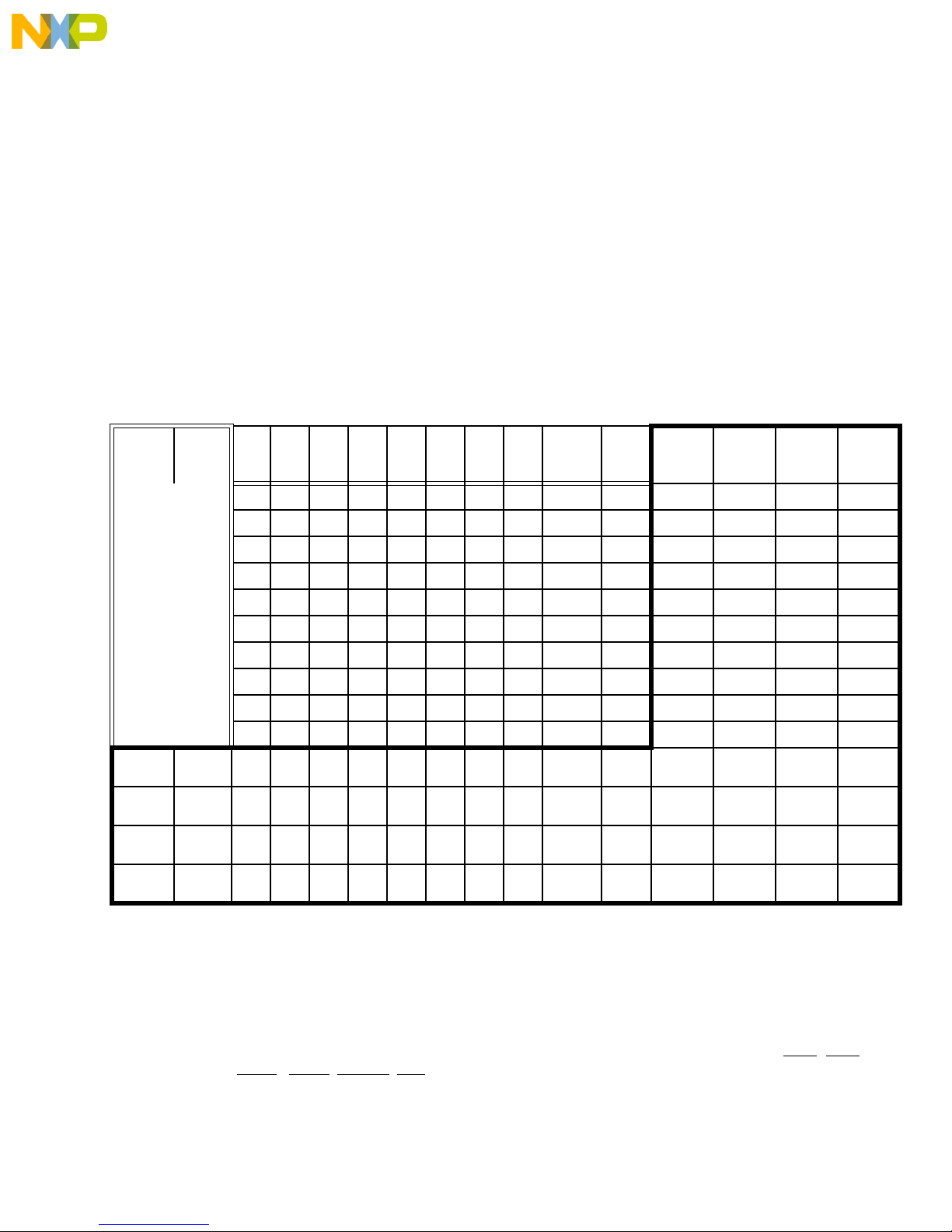
The base address for the T1devices is 60,000,000H.
The devices that need a CS are:
PM4388 TOCTL use !A20 & !A19 & !A18 & !BRDCS1 (CS6), T1_1 - T1_8 FRAMER
PM4314 QDSX use !A20 & !A19 & A18 & !BRDCS1 (CS6), T1_1 - T1_4 LIU
PM4314 QDSX use !A20 & A19 & !A18 & !BRDCS1 (CS6), T1_5 - T1_8 LIU
The base address for the DS3 devices is 70,000,000H.
TXC-03401 DS3F use !A20 & A19 & A18 & !BRDCS2 (CS7), DS3_1
TXC-03401 DS3F use A20 & !A19 & !A18 & !BRDCS2 (CS7), DS3_2
NOTE: Fast Ethernet modules on this board do not use any signal from the logic controls except for RESET
signal to the FE transceiver.
Table 3: Enable Selection
nc...
, I
or
emiconduct
eescale S
Fr
Voyager
Port
PD4 = 0 T1_1 EN DIS X
PD5 = 0 T1_2 EN X X
PD6 = 0 T1_3 EN X DIS
PD7 = 0 T1_4 EN X DIS
PD8 = 0 T1_5 EN X DIS
PD9 = 0 T1_6 EN X X
PD18 = 0 T1_7 EN DIS X
PD19 = 0 T1 _8 EN DIS DIS
PD25 = 0 DS3 1 DIS DIS DIS EN
PA4 = 0 DS3 2 DIS DIS DIS DIS EN
PA5 =0
PA1 = 0
PA5 = 1
PA1 = 0
PC13 = 0
PA1 = 0
PC13 = 1
PA1 = 0
The
Port
control
T11T12T13T14T15T16T17T1
DS3_1
enable
8
signal
DS3 2
enable
signal
DS3_1
LB RT1
EN
DS3_1
LB TR1
EN
DS3_2
LB RT2
EN
DS3_2
LB TR2
EN
3•9 8260ADS to 8260TCOM Connectors
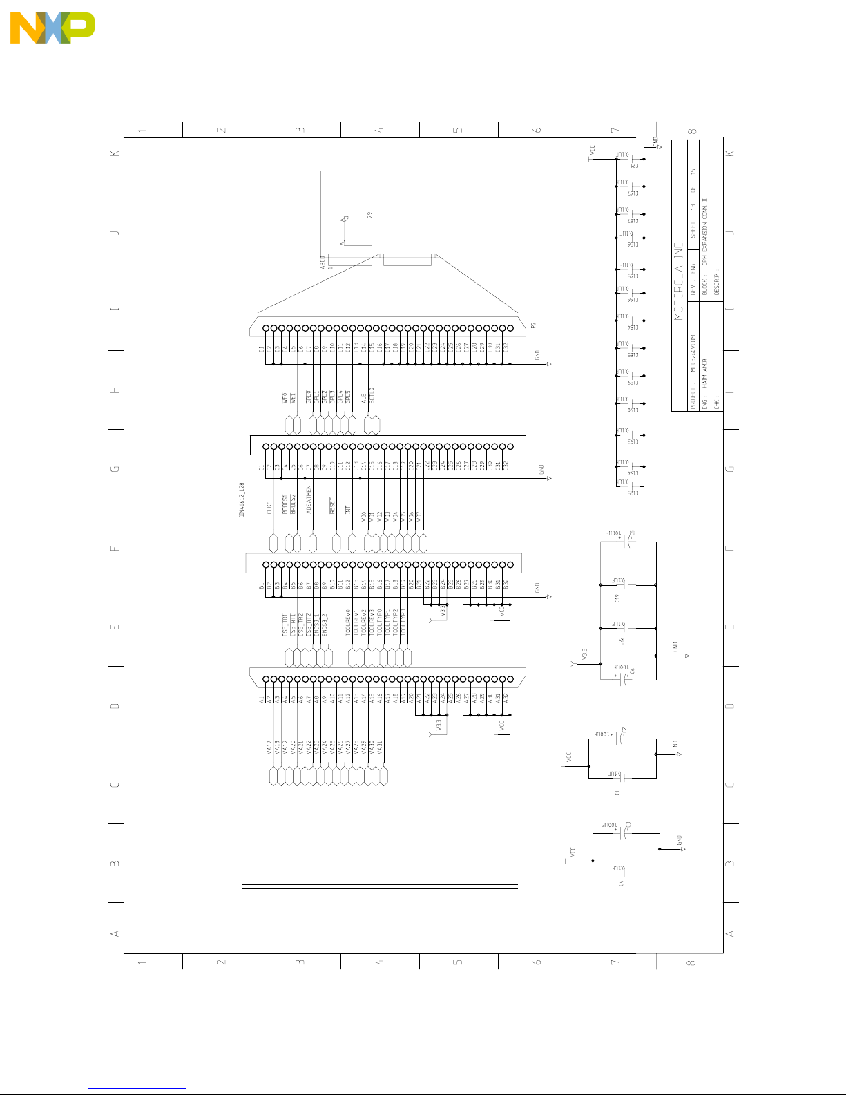
The physical connection from the MPC8260ADS to the MPC860TCOM board is done by the two 128 pin
connectors. One connector contains 16 Address lines, 16 Data lines, CS6 and CS7 signals, WE0, WE1,
ALE, BCTL0, GPL0 - GPL5, RESET, IRQ and CLOCK. Other signals are for showing the connected board
status and rev. The status shown is one of 4 DS3 loopback option, DS3_1 and DS3_2 enable. The other
For More Information On This Product,
Go to: www.freescale.com
17
Page 18
MPC8260TCOM User’s Manual PRELIMINARY
Freescale Semiconductor, Inc.
FUNCTIONAL DESCRIPTION
connector contains all MPC8260 parallel ports. These connectors also include the power signals for the
8260TCOM board (ground, 3.3V and 5V).
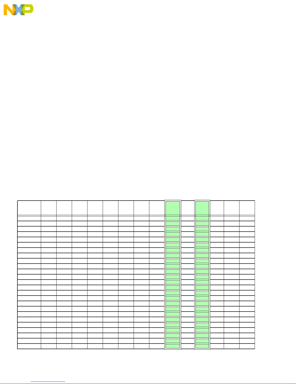
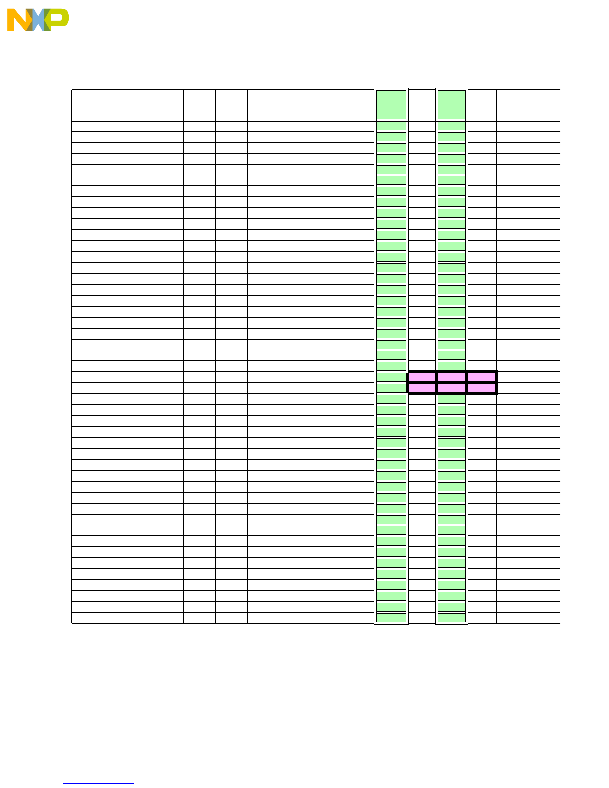
3•10 Ports Selection
The following table shows all the ports that are used on the 8260TCOM. It includes there function for each
used module. The table includes:
1. The port column, i.e. the port number.
2. The module name function which contains the 8 T1 ports (8 column).
3. The ATM 8 bit port on the ADS (this column is a dark column to accent the ADS function which uses
FCC1); each named cell of the column describes the function.
4. The Fast Ethernet address ’1’ column use FCC1.
5. The Fast Ethernet address ’0’ column which is also a dark one since it is on the ADS; it use FCC2.
6. The Fast ethernet address ’2’ column use FCC3.
7. The DS3 _1 column use FCC2.
8. The DS3_2 column use FCC3.
nc...
, I
or
In each table row there are I or O signs at the right side of the function name meaning that this signal is an
output from the MPC8260 device (O) or an input to the MPC8260 (I). In some rows there are several I/O
signs which mean the respective port can be use for several function. The user should avoid conflicts; as
an example if the ATM is used on the ADS it is not possible to use the FE address 1. This table can help
the user to define the desire module without having a conflict, or if there is a problem in the definition the
user can know which one of the module can cause the problem.
PC9 and PC10 are the MII MDIO and MDC signals; these signals are common to the 3 FE modules - the
one on the ADS and the two on the TCOM.
Table 4: Ports Function Signals
Ports
emiconduct
PA2 (clock20) TXCLK I TXCLK I
PA6 RSYNC I
PA7 TSYNC I
PA8 RXD I
PA9 TXD O
PA14
PA15 RXD5 I RXD2 I
PA16 RXD6 I RXD1 I
eescale S
PA17 RXD7 I RXD0 I
PA18 TXD7 O TXD0 O
Fr
PA19 TXD6OTXD1 O
PA20 TXD5OTXD2 O
PA21 TXD4 O TXD3 O
PA26 RxClav I RXER I
PA27 RxSoc I RXDV I
PA28 RxEnb O TXEN O
PA29 TxSoc O TXER O
PA3(clock19) RXCLK I RXD1 I
PA30
PA31 TxEnb O COL I
PB4 RSYNC I TXD3 O RSYNC I
PB5
PB6 RXD I
PB7 TXD I
PB8 RSYNC I
T1
A1
T1
1
B1
T1
2
C1
T1
3
D1
T1
4
A2
TSYNC I TXD2 O TSYNC I
T1
5
B2
T1
6
C2
T1
7
ADS ATM8FE1
8
D2
RXD4 I RXD3 I
TxClav I CRS I
FCC1
ADS FE 0
FCC2
FCC3
TXD1 O RXD0 I
TXD0 O TXD0 I
RXD0 I
TDM1
FE
2
DS3
1
FCC2
RSYNC I
TSYNC I
RXD0 I
TXD0 O
TDM2
DS3
2
FCC3
18
For More Information On This Product,
Go to: www.freescale.com
Page 19
PRELIMINARY MPC8260TCOM User’s Manual
Freescale Semiconductor, Inc.
FUNCTIONAL DESCRIPTION
Table 4: Ports Function Signals
nc...
, I
or
emiconduct
eescale S
Fr
T1
Ports
PB9 TSYNC I RXD1 I TXD2 O
PB10 RXD I
PB11 TXD O
PB12 RSYNC I
PB13 TSYNC I
PB14 RXD I
PB15 TXD O
PB16
PB17
PB18
PB19
PB20 RSYNC I
PB21 TSYNC I
PB22 RXD I
PB23 TXD O
PB24 RSYNC I
PB25 TSYNC I
PB26 RXD I
PB27 TXD O
PB28 TSYNC I
PB29 RSYNC I
PB30 RXD I
PB31 TXD O
PC9/
PC10/
PC1
PC16 (clock16) TCLK I
PC17 (clock15) RCLK I
PC18 (clock14) TCLK I
PC19 (clock13) RCLK I
PC20 (clock12)
PC21 (clock11) RxClk I RCLK I
PC22 (clock10) TCLK I
PC23 (clock9) RCLK I
PC24 (clock8) TCLK I
PC25 (clock7) RCLK I
PC26 (clock6) TCLK I TCLK I
PC27 (clock5) RCLK I
PC28 (clock4) TCLK I
PC29 (clock3) RCLK I
PC30 (clock2) TCLK I
PC31 (clock1) RCLK I RCLK I
PD10 RSYNC I
PD11 TSYNC I
PD12 RXD I
PD13 TXD O
1
A1
T1
B1
T1
2
C1
T1
3
D1
T1
4
A2
T1
5
B2
T1
6
C2
T1
7
8
D2
ADS ATM8FE1
MDIO B MDIO B MDIO B
MDC O MDC O MDC O
TxClk I TCLK I
ADS FE 0
FCC2
FCC1
RXD3 I RXD2 I
RXD2 I RXD3 I
RXD1 I TXD1 O
RXD0 I TXD2 O
TXD0 O RXD1 I
TXD1 O RXD2 I
TXD2 O RXD3 I
TXD3 O TXD3 O
CRS I
COL I
RXER I
TXEN O
RXDV I
TXER O
TCLK I
RCLK I
FCC3
RXD2 I
RXD3 I
CRS I
COL I TXD1 O
TXEN O
TXER O
RXER I
RXDV I
TCLK I
RCLK I
TDM1
FE
2
FCC2
DS3
TDM2
DS3
1
2
FCC3
TXD3 O
RCLK I
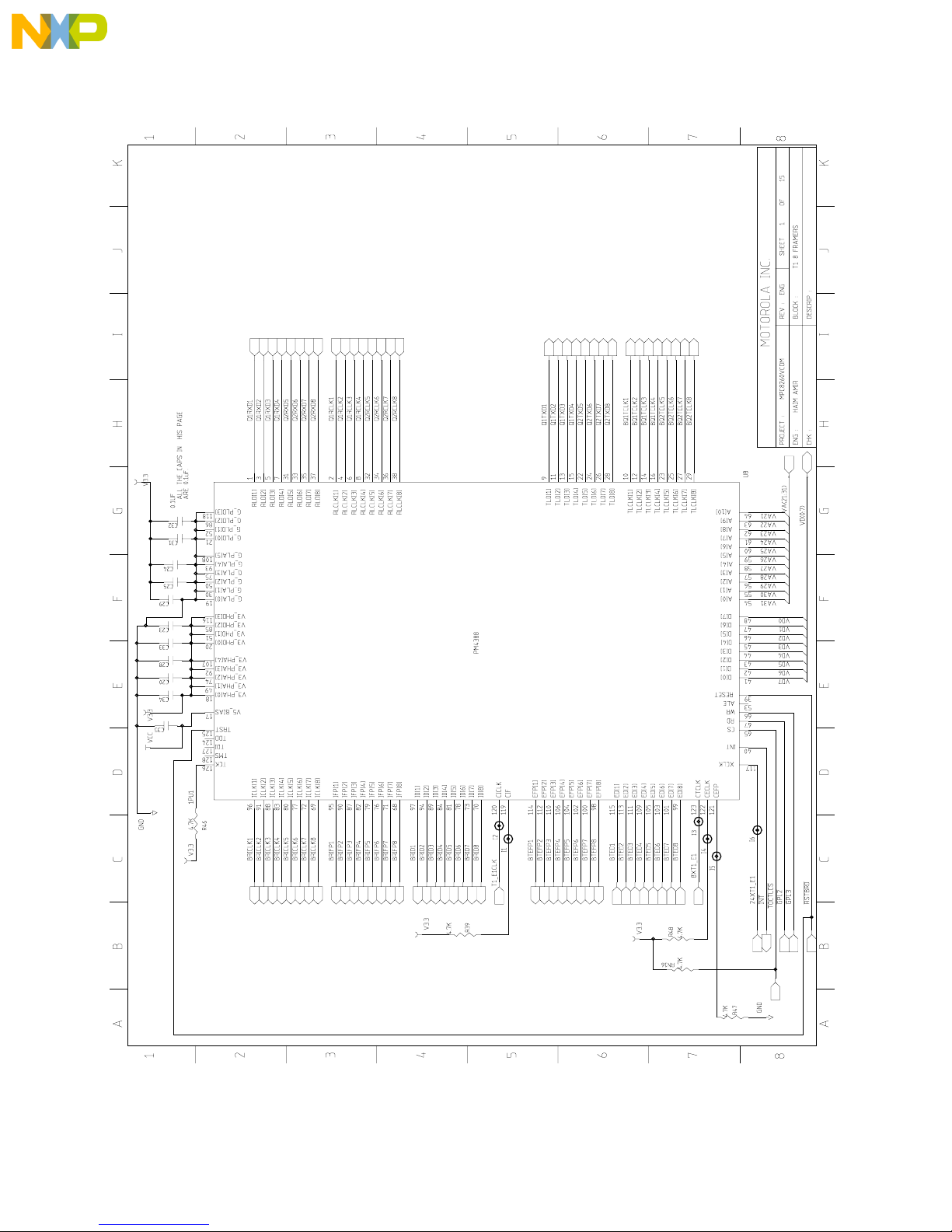
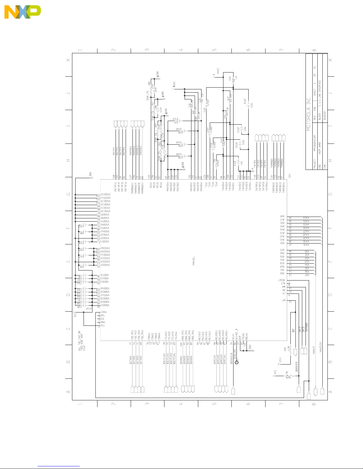
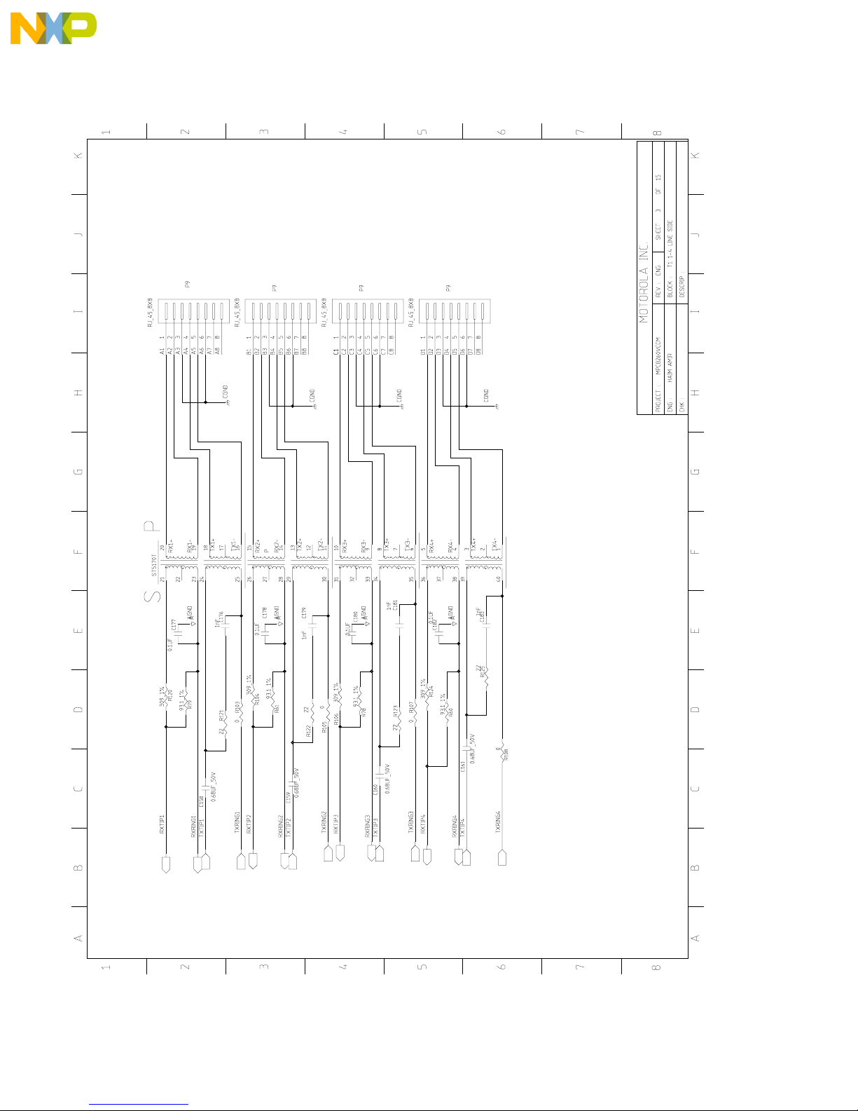
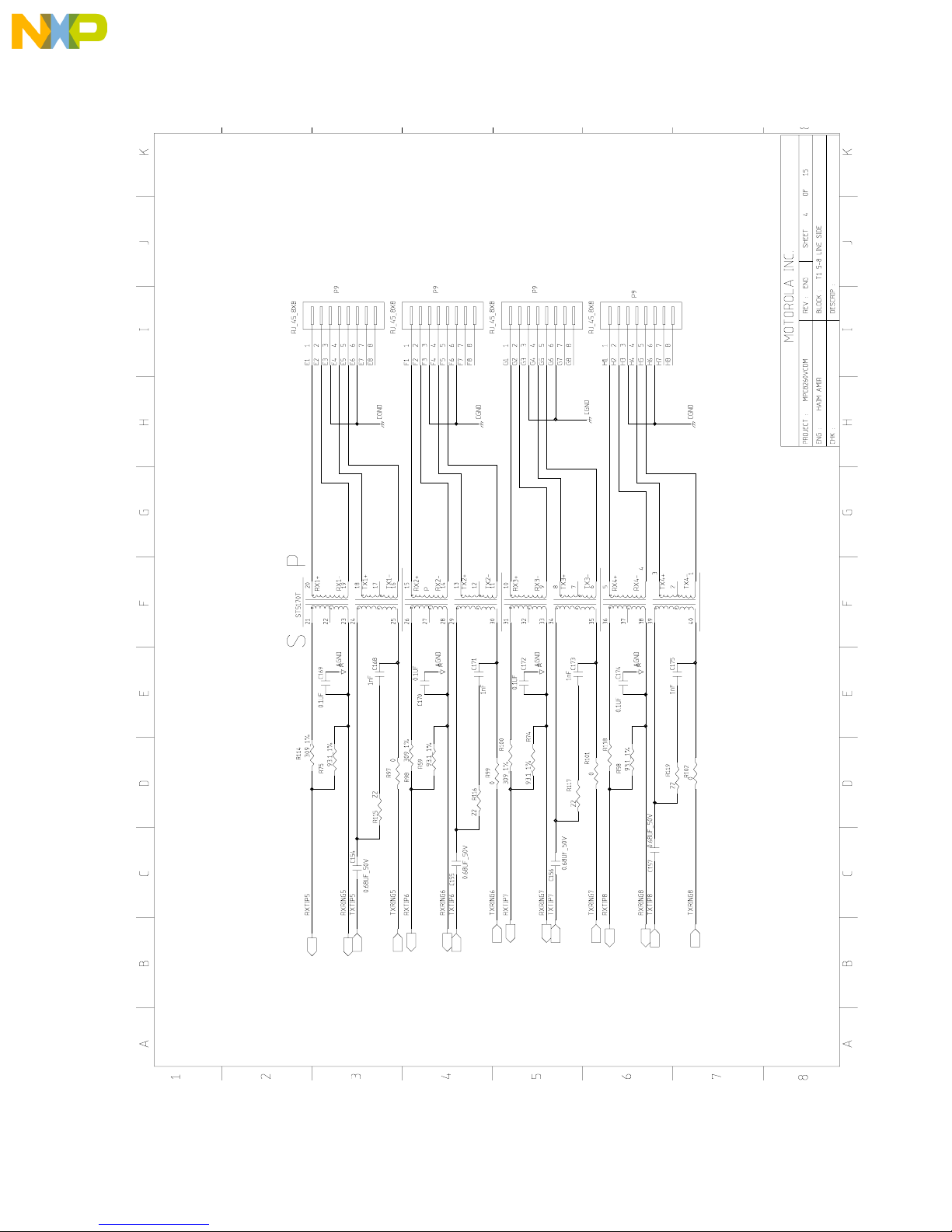
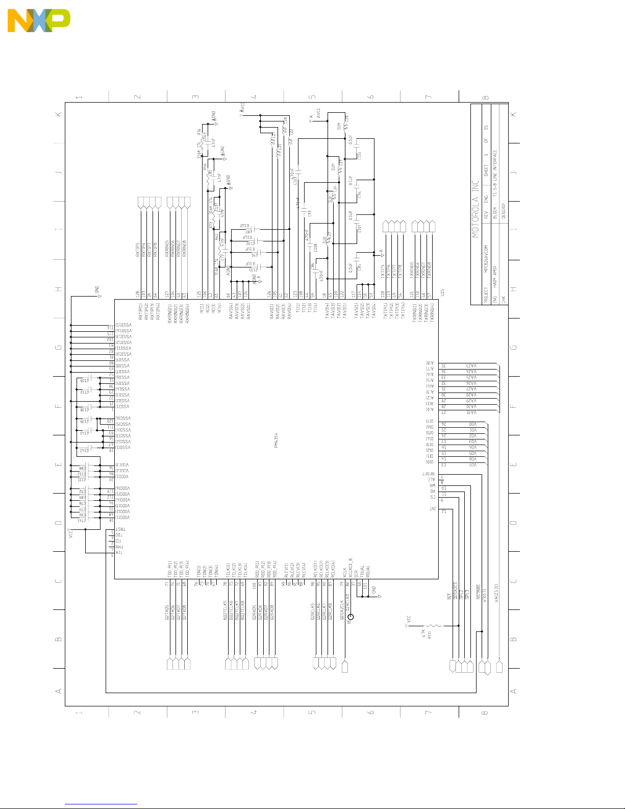
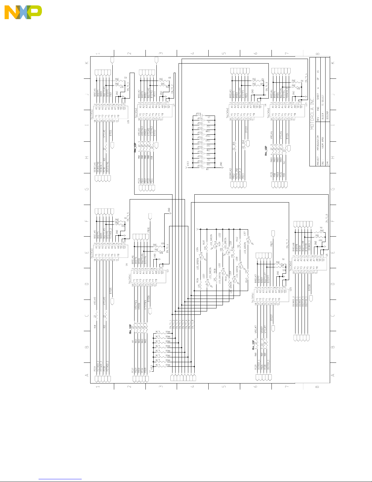
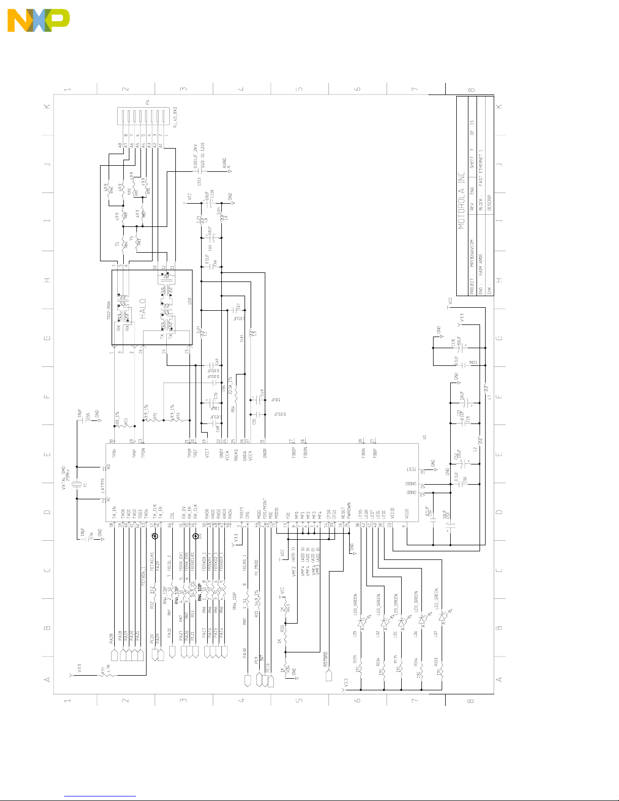
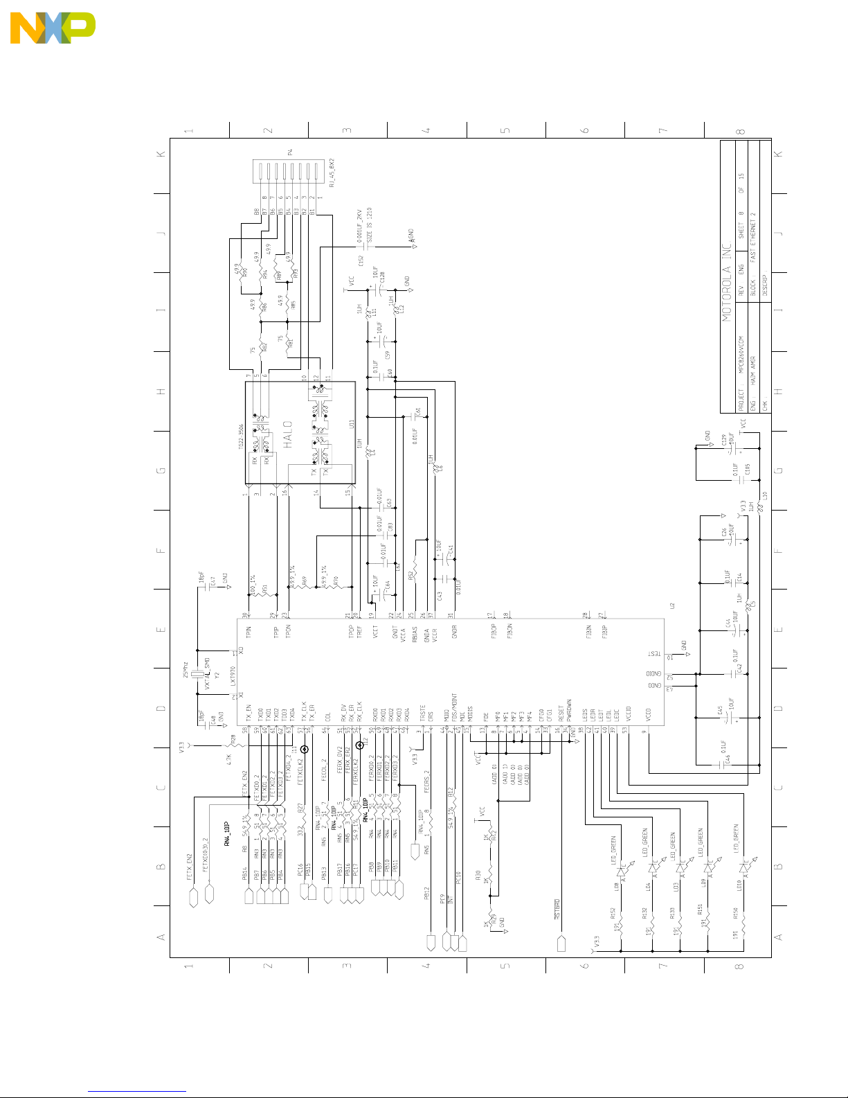
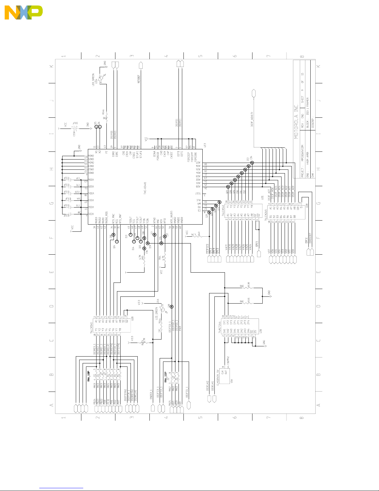
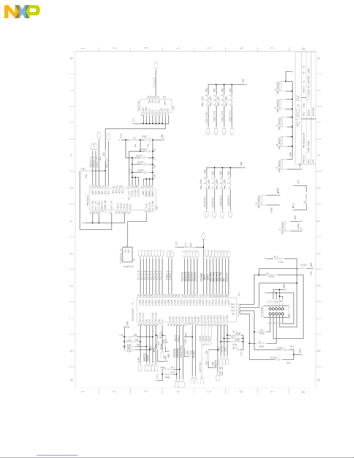
3•11 SCHEMATICS
For More Information On This Product,
Go to: www.freescale.com
19
Page 20
MPC8260TCOM User’s Manual PRELIMINARY
FUNCTIONAL DESCRIPTION
Freescale Semiconductor, Inc.
nc...
, I
or
emiconduct
eescale S
Fr
20
For More Information On This Product,
Go to: www.freescale.com
Page 21
PRELIMINARY MPC8260TCOM User’s Manual
Freescale Semiconductor, Inc.
FUNCTIONAL DESCRIPTION
nc...
, I
or
emiconduct
eescale S
Fr
For More Information On This Product,
Go to: www.freescale.com
21
Page 22
MPC8260TCOM User’s Manual PRELIMINARY
FUNCTIONAL DESCRIPTION
Freescale Semiconductor, Inc.
nc...
, I
or
emiconduct
eescale S
Fr
22
For More Information On This Product,
Go to: www.freescale.com
Page 23
PRELIMINARY MPC8260TCOM User’s Manual
Freescale Semiconductor, Inc.
FUNCTIONAL DESCRIPTION
nc...
, I
or
emiconduct
eescale S
Fr
For More Information On This Product,
Go to: www.freescale.com
23
Page 24
MPC8260TCOM User’s Manual PRELIMINARY
FUNCTIONAL DESCRIPTION
Freescale Semiconductor, Inc.
nc...
, I
or
emiconduct
eescale S
Fr
24
For More Information On This Product,
Go to: www.freescale.com
Page 25
PRELIMINARY MPC8260TCOM User’s Manual
Freescale Semiconductor, Inc.
FUNCTIONAL DESCRIPTION
nc...
, I
or
emiconduct
eescale S
Fr
For More Information On This Product,
Go to: www.freescale.com
25
Page 26
MPC8260TCOM User’s Manual PRELIMINARY
FUNCTIONAL DESCRIPTION
Freescale Semiconductor, Inc.
nc...
, I
or
emiconduct
eescale S
Fr
26
For More Information On This Product,
Go to: www.freescale.com
Page 27
PRELIMINARY MPC8260TCOM User’s Manual
Freescale Semiconductor, Inc.
FUNCTIONAL DESCRIPTION
nc...
, I
or
emiconduct
eescale S
Fr
For More Information On This Product,
Go to: www.freescale.com
27
Page 28
MPC8260TCOM User’s Manual PRELIMINARY
FUNCTIONAL DESCRIPTION
Freescale Semiconductor, Inc.
nc...
, I
or
emiconduct
eescale S
Fr
28
For More Information On This Product,
Go to: www.freescale.com
Page 29
PRELIMINARY MPC8260TCOM User’s Manual
Freescale Semiconductor, Inc.
FUNCTIONAL DESCRIPTION
nc...
, I
or
emiconduct
eescale S
Fr
For More Information On This Product,
Go to: www.freescale.com
29
Page 30
MPC8260TCOM User’s Manual PRELIMINARY
FUNCTIONAL DESCRIPTION
Freescale Semiconductor, Inc.
nc...
, I
or
emiconduct
eescale S
Fr
30
For More Information On This Product,
Go to: www.freescale.com
Page 31
PRELIMINARY MPC8260TCOM User’s Manual
Freescale Semiconductor, Inc.
FUNCTIONAL DESCRIPTION
nc...
, I
or
emiconduct
eescale S
Fr
For More Information On This Product,
Go to: www.freescale.com
31
Page 32
MPC8260TCOM User’s Manual PRELIMINARY
FUNCTIONAL DESCRIPTION
Freescale Semiconductor, Inc.
ADS
nc...
, I
or
emiconduct
eescale S
Fr
32
For More Information On This Product,
Go to: www.freescale.com
Page 33
PRELIMINARY MPC8260TCOM User’s Manual
Freescale Semiconductor, Inc.
FUNCTIONAL DESCRIPTION
nc...
, I
or
emiconduct
eescale S
Fr
For More Information On This Product,
Go to: www.freescale.com
33
Page 34
MPC8260TCOM User’s Manual PRELIMINARY
FUNCTIONAL DESCRIPTION
Freescale Semiconductor, Inc.
ADS
nc...
, I
or
emiconduct
eescale S
Fr
34
For More Information On This Product,
Go to: www.freescale.com
Page 35
nc...
, I
or
PRELIMINARY MPC8260TCOM User’s Manual
Freescale Semiconductor, Inc.
SUPPORT INFORMATION
CHAPTER 4 - SUPPORT INFORMATION
4•1 INTRODUCTION
This chapter provides the interconnection signals and the parts list of the MPC8260TCOM board.
4•2 INTERCONNECT SIGNALS
The MPC8260TCOM board interconnects with external devices through the following connectors:
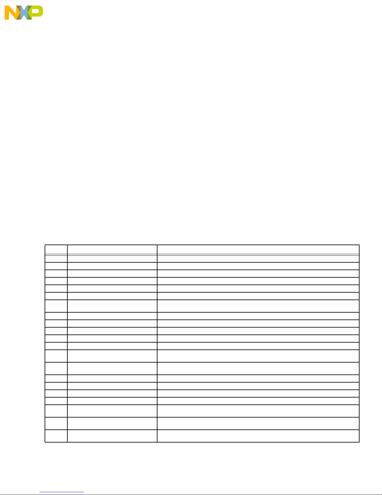
• P1 is a 128 pin connector which includes all the MPC8260 I/O signals needed by the 8260TCOM
board. It connects the 8260TCOM to the 8260ADS.
• P2 is a 128 pin connector which include the address, data, control and status signals. it connects
the 8260TCOM to the 8260ADS.
• P3 is the ISP connector for programming the MACH.
• P4 is the RJ45 connector for the Fast Ethernet; this connector is for the 2 fast ethernet ports.
• P5 - P8 are the BNC connectors for the 2 x DS3, 2 of the connectors are for transmit and 2 for
receive.
• P9 is a 8 x 8 pin, RJ45 connector for the 8 x T1.
4•2•1 P1 PORTS CONNECTOR
emiconduct
eescale S
Fr
A
A1 NC
A2 NC
A3 NC
A4 NC
A5 NC
A6 NC
A7 PD25
VDS3EN1~
A8 NC
A9 NC
A10 NC
A11 NC
A12 NC
A13 PD19
EN_T1_8
A14 PD18
EN_T1_7
A15 NC
A16 NC
A17 NC
A18 NC
A19 PD13
TDMB1-L1TXD
A20 PD12
TDMB1-L1RXD
A21 PD11
TDMB1-L1TSYNC
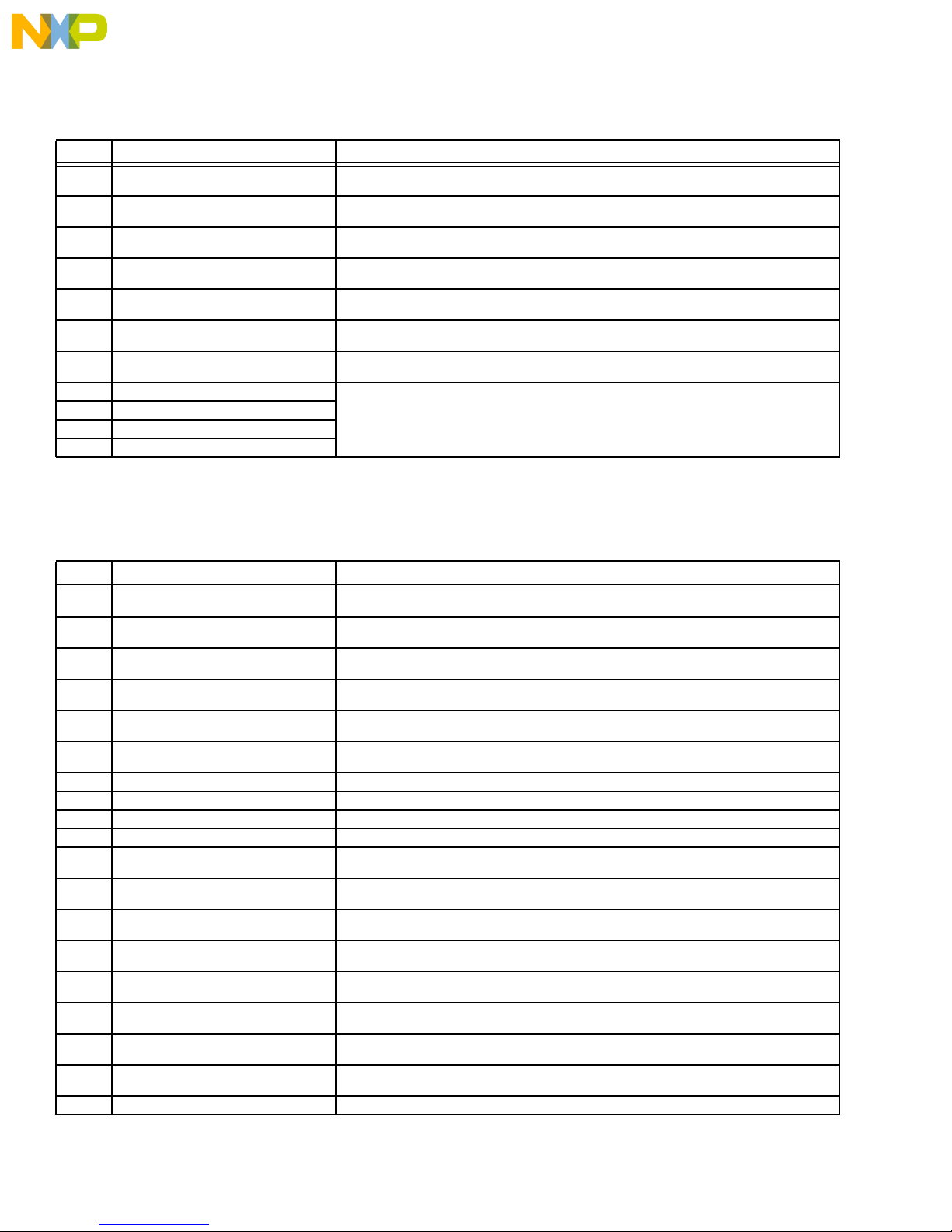
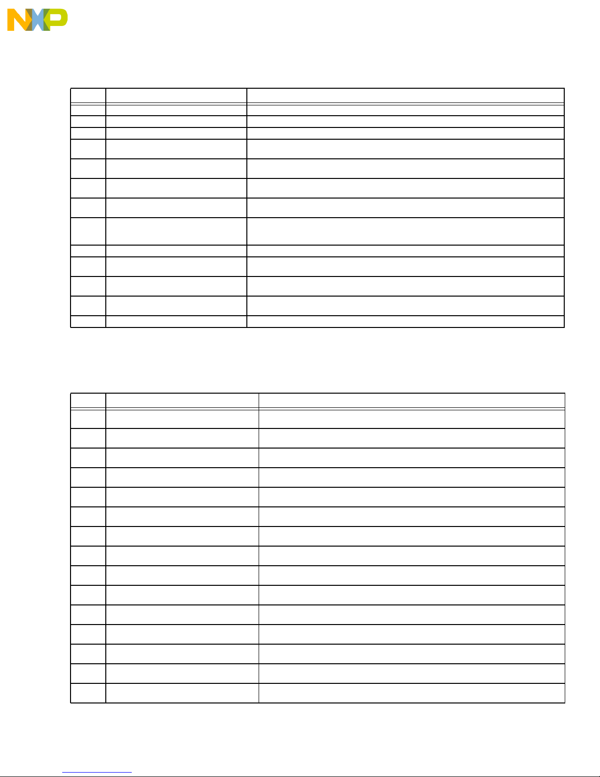
Table 5: P1 PORT D (A row)
This signal is the DS3_1 enable request; if T1_1, T1_7 and T1_8 are not enabled the DS3_1 is
automatically enabled if PD25 is low.
Enable T1_8; if this signal is low T1_8 is enabled and DS3_1 and DS3_2 are disabled
Enable T1_7; if this signal is low T1_7 is enabled and DS3_1 is disabled
T1_2 TXD; this function use TDMB1
T1_2 RXD; this function use TDMB1
T1_2 TSYNC; this function use TDMB1
For More Information On This Product,
Go to: www.freescale.com
35
Page 36
MPC8260TCOM User’s Manual PRELIMINARY
Freescale Semiconductor, Inc.
SUPPORT INFORMATION
Table 5: P1 PORT D (A row)
A
A22 PD10
A23 PD9
A24 PD8
A25 PD7
A26 PD6
A27 PD5
A28 PD4
A29 VCC through these pins the TCOM gets the POWER (VCC).
A30 VCC
A31 VCC
nc...
A32 VCC
TDMB1-L1RSYNC
EN_T1_6
EN_T1_5
EN_T1_4
EN_T1_3
EN_T1_2
EN_T1_1
T1_2 RSYNC; this function use TDMB1
Enable T1_6 signal. If this signal is low then T1_6 is enabled
Enable T1_5; if this signal is low T1_5 is enable and DS3_2 is disabled
Enable T1_4; if this signal is low T1_4 is enable and DS3_2 is disabled
Enable T1_3; if this signal is low T1_3 is enable and DS3_2 is disabled
Enable T1_2 signal. If this signal is low then T1_2 is enabled
Enable T1_1; if this signal is low T1_1 is enable and DS3_1 is disabled
, I
or
B
B1 PA31
B2 PA30
B3 PA29
emiconduct
B4 PA28
B5 PA27
B6 PA26
B7 NC
B8 NC
B9 NC
eescale S
B10 NC
B11 PA21
Fr
B12 PA20
B13 PA19
B14 PA18
B15 PA17
B16 PA16
B17 PA15
B18 PA14
B19 NC
MIICOL/ATM8-TxEnb
MIICRS/ATM8-TxClav
MIITXER/ATM8-TxSOC
MIITXEN/ATM8-RxEnb
MIIRXDV/ATM8-RxSOC
MIIRXER/ATM8-RxClav
MIITXD3/ATM8--TXD4
MIITXD2/ATM8-TXD5
MIITXD1/ATM8-TXD6
MIITXD0/ATM8-TXD7
MIIRXD0/ATM8-RXD7
MIIRXD1/ATM8-RXD6
MIIRXD2/ATM8-RXD5
MIIRXD3/ATM8-RXD4
Table 6: P1 PORT A (B row)
Fast Ethernet FCC1 MIICOL signal or ATM8 on ADS TxEnb signal.
Fast Ethernet FCC1 MIICRS signal or ATM8 on ADS TxClav signal
Fast Ethernet FCC1 MIITXER signal or ATM8 on ADS Txsoc signal
Fast Ethernet FCC1 MIITXEN signal or ATM8 on ADS RxEnb signal
Fast Ethernet FCC1 MIIRXDV signal or ATM8 on ADS RxSoc signal
Fast Ethernet FCC1 MIIRxClav signal or ATM8 on ADS RxClav signal
Fast Ethernet FCC1 MIITXD3 signal or ATM8 on ADS TXD4 signal
Fast Ethernet FCC1 MIITXD2 signal or ATM8 on ADS TXD5 signal
Fast Ethernet FCC1 MIITXD1 signal or ATM8 on ADS TXD6 signal
Fast Ethernet FCC1 MIITXD0 signal or ATM8 on ADS TXD7 signal
Fast Ethernet FCC1 MIIRXD0 signal or ATM8 on ADS RXD7 signal
Fast Ethernet FCC1 MIIRXD1 signal or ATM8 on ADS RXD6 signal
Fast Ethernet FCC1 MIIRXD2 signal or ATM8 on ADS RXD5 signal
Fast Ethernet FCC1 MIIRXD3 signal or ATM8 on ADS RXD4 signal
36
For More Information On This Product,
Go to: www.freescale.com
Page 37
nc...
, I
or
PRELIMINARY MPC8260TCOM User’s Manual
Freescale Semiconductor, Inc.
SUPPORT INFORMATION
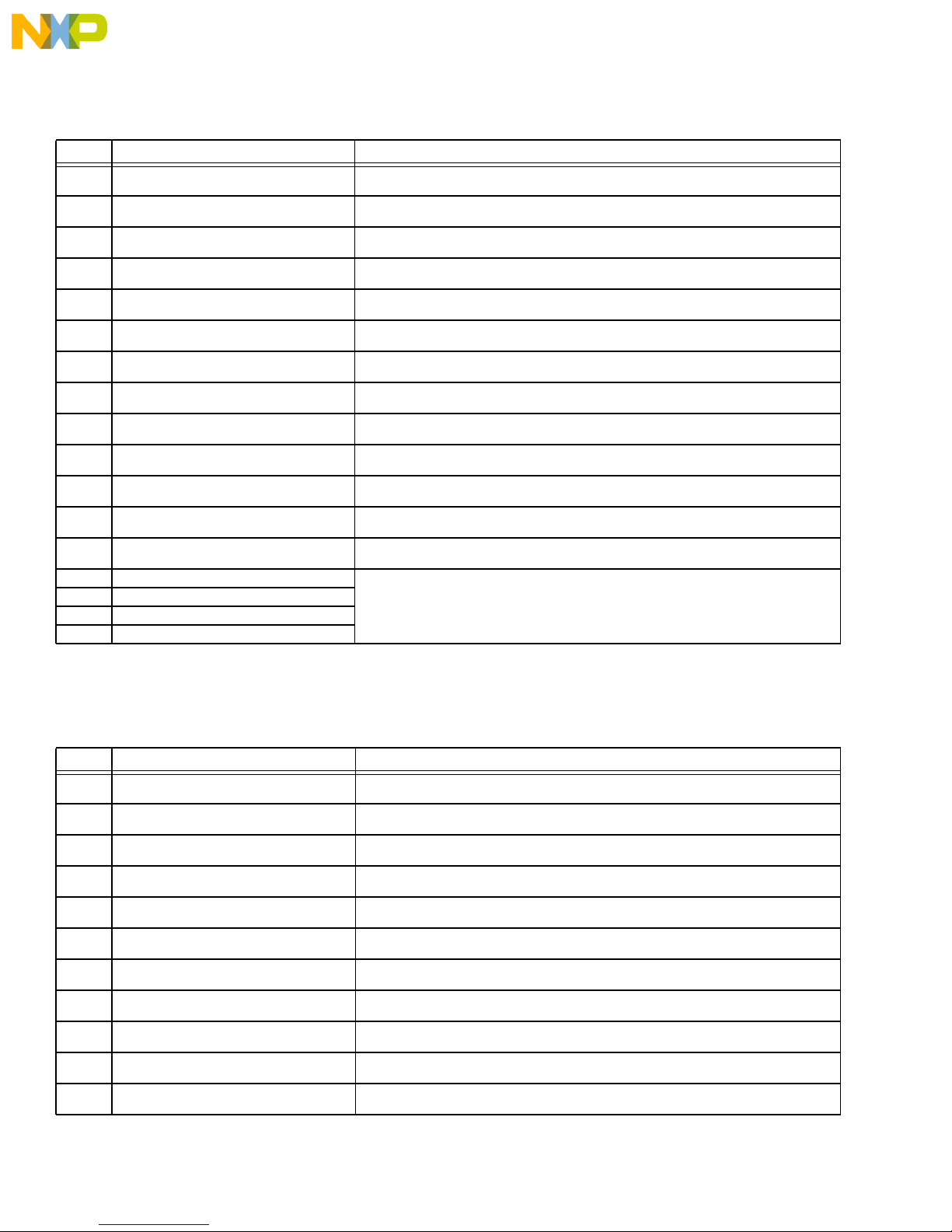
Table 6: P1 PORT A (B row)
B
B20 NC
B21 NC
B22 NC
B23 PA9
DS3-TXD0/TDMA1-L1TXD0
B24 PA8
DS3-RXD0/TDMA1-L1RXD0
B25 PA7
DS3-TXSYNC/TDMA1-L1TSYNC
B26 PA6
DS3-RXSYNC/TDMA1-L1RSYNC
B27 PA5 PA5 is used to select one of the DS3 _1 Loopback modes.
B28 PA4 DS3 2 is enabled by driving PA4 to low and if all of T1-1, T1-7, T1-8 are disabled
B29 PA3
DS3-RXD1/TDMD2-RXCLK(clock19)
B30 PA2
DS3-TXCLK/TDMD2-TXCLK(clock20)
B31 PA1
Enable DS3 loop back
B32 NC
DS3_1 FCC2 TXD0 signal or T1_1 TXD signal; if T1_1 is enable DS3_1 is disable.
DS3_1 FCC2 RXD0 signal or T1_1 RXD signal; if T1_1 is enable DS3_1 is disable.
DS3_1 FCC2 TSYNC signal or T1_1 TSYNC signal; if T1_1 is enable DS3_1 is disable.
DS3_1 FCC2 RSYNC signal or T1_1 RSYNC signal; if T1_1 is enable DS3_1 is disable.
DS3_1 RT will be low if PA5 and PA1 will be low.
DS3_1 TR will be low if PA5 will be high and PA1 will be low.
DS3_2 FCC3 RXD1 signal or T1_8 RXCLK signal. if T1_8 is enable DS3_2 is disable.
DS3_1 FCC2 TXCLK signal or T1_8 TXCLK signal. if T1_8 is enable DS3_1 is disable.
If PA1 is low a loop back modes on DS3 1 & 2 is enabled
emiconduct
eescale S
Fr
Table 7: P1 PORT B (C row)
C
C1 PB31
TDMB2-L1TXD/MIITXER
C2 PB30
TDMB2-L1RXD/ATM8-MIIRXDV
C3 PB29
TDMB2-L1RSYNC/MIITXEN
C4 PB28
TDMB2-L1TSYNC/MIIRXER
C5 PB27
TDMC2-L1TXD/MIICOL
C6 PB26
TDMC2-L1RXD/MIICRS
C7 PB25
DS3-TXD3/TDMC2-L1TSYNC/MIITXD3
C8 PB24
DS3-RXD3/TDMC2-L1RSYNC/MIITXD2
C9 PB23
DS3-RXD2/TDMD2-L1TXD/MIITXD1
C10 PB22/DS3-RXD1/TDMD2-L1RXD/MIITXD0 T1_8 RXD signal or FCC2 DS3_1 RXD1 signal. If T1_8 signal is enable DS3_1 is disable. This
C11 PB21
DS3-TXD2/TDMD2-L1TSYNC/MIIRXD0
C12 PB20
DS3-TXD1/TDMD2-L1RSYNC/MIIRXD1
C13 PB19
DS3-RXD3/MIIRXD2
C14 PB18
DS3-RXD2/MIIRXD3
C15 PB17
MIIRXDV
T1_6 TXD signal or FCC2 MIITXER signal on ADS.
T1_6 RXD signal or FCC2 MIIRXDV signal on ADS.
T1_6 RSYNC signal or FCC2 MIITXEN signal on ADS.
T1_6 TSYNC signal or FCC2 MIIRXER signal on ADS.
T1_7 TXD signal or FCC2 MIICOL signal on ADS.
T1_7 RXD signal or FCC2 MIITCRS signal on ADS.
T1_7 TSYNC signal or FCC2 DS3_1 TXD3 signal. If T1_7 is enable DS3_1 is disable. This signal
can be FCC2 MIITXD3 signal on ADS.
T1_7 RSYNC signal or FCC2 DS3_1 RXD3 signal If T1_7 is enable DS3_1 is disable. This signal
can be FCC2 MIITXD2 signal on ADS.
T1_8 TXD signal or FCC2 DS3_1 RXD2 signal. If T1_8 is enable DS3_1 is disable. This signal
can be FCC2 MIITXD1 signal on ADS.
signal can be FCC2 MIITXD0 signal on ADS.
T1_8 TSYNC signal or FCC2 DS3_1 TXD2 signal. If T1_8 signal is enable DS3_1 is disable. This
signal can be FCC2 MIIRXD0 signal.
T1_8 RSYNC signal or FCC2 DS3_1 TXD1 signal. If T1_8 signal is enable DS3_1 is disable. This
signal can be FCC2 MIIRXD1 signal.
DS3_1 RXD3 signal on FCC3 or MIIRXD2 signal on FCC2 on ADS.
DS3_1 RXD2 signal on FCC3 or MIIRXD3 signal on FCC2 on ADS.
FE_2 MIIRXDV signal on FCC3.
For More Information On This Product,
Go to: www.freescale.com
37
Page 38
MPC8260TCOM User’s Manual PRELIMINARY
Freescale Semiconductor, Inc.
SUPPORT INFORMATION
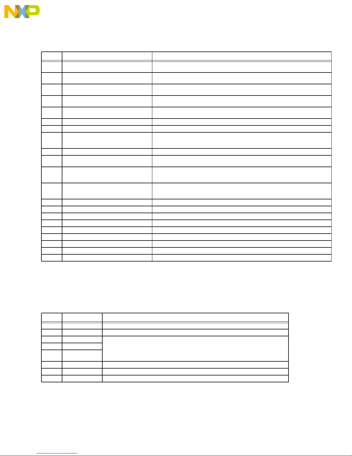
Table 7: P1 PORT B (C row)
C
C16 PB16
C17 PB15
C18 PB14
C19 PB13
C20 PB12
C21 PB11
C22 PB10
C23 PB9
C24 PB8
nc...
C25 PB7
, I
C26 PB6
or
C27 PB5
C28 PB4
C29 GND through these pins the TCOM gets POWER (GND).
C30 GND
C31 GND
C32 GND
MIIRXER
MIITXER/TDMC1-L1TXD
MIITXEN/TDMC1-L1RXD
MIICOL/DS3-TXD1/TDMC1-L1TSYNC
MIICRS/TDMC1-L1RSYNC
MIIRXD3/TDMD1-L1TXD
MIIRXD2/TDMD1-L1RXD
MIIRXD1/DS3-TXD2/TDMD1-L1TSYNC
MIIRXD0/TDMD1-L1RSYNC
MIITXD0/DS3-TXD0/TDMA2-L1TXD
MIITXD1/DS3-RXD0/TDMA2-L1RXD
MIITXD2/DS3-TXSYNC//TDMA2-L1TSYNC
MIITXD3/DS3-RXSYNC/TDMA2-L1RSYNC
FE_2 MIIRXER signal on FCC3.
T1_3 TXD signal or FE_2 MIITXER signal on FCC3 .
T1_3 RXD signal or FE_2 MIITXEN signal on FCC3 .
T1_3 TSYNC or FE_2 MIICOL signal on FCC3 or DS3_2 TXD1 signal on FCC3.
T1_3 RSYNC signal or FE_2 MIICRS signal on FCC3.
T1_3 TXD signal or FE_2 MIIRXD3 signal on FCC3.
T1_4 RXD signal or FE_2 MIIRXD2 signal on FCC3.
T1_4 TSYNC signal or FE_2 MIIRXD1 signal on FCC3 or DS3_2 TXD2 signal. If T1_4 is enable
DS3_2 is disable.
T1_4 RSYNC signal or FE_2 MIIRXD0 signal on FCC3.
T1_5 TXD signal or FE_2 MIITXD0 signal on FCC3 or DS3_2 TXD0 signal on FCC3. If T1_5 is
enable then DS3_2 is disable.
T1_5 RXD signal or FE_2 MIITXD1 signal on FCC3 or DS3_2 RXD0 signal on FCC3. If T1_5 is
enable then DS3_2 is disable.
T1_5 TSYNC signal or FE_2 MIITXD2 signal on FCC3 or DS3_2 TSYNC signal on FCC3. If T1_5
is enable then DS3_2 is disable.
T1_5 RSYNC signal or FE_2 MIITXD3 signal on FCC3 or DS3_2 RSYNC signal on FCC3. If T1_5
is enable then DS3_2 is disable.
emiconduct
Table 8: P1 PORT C (D row)
D
D1 PC31
D2 PC30
eescale S
D3 PC29
Fr
D4 PC28
D5 PC27
D6 PC26
D7 PC25
D8 PC24
D9 PC23
D10 PC22
D11 PC21
DS3-RXCLK(clock1)/TDMA1-RXCLK(clock1)
TDMA1-TXCLK(clock2)
TDMC2-RXCLK(clock3)
TDMC2-TXCLK(clock4)
DS3-RXCLK(clock5)/TDMC1-L1RXCLK(clock5)
DS3-TXCLK(clock6)/TDMC1-L1TXCLK(clock6)
TDMD1-RXCLK(clock7)
TDMD1-TXCLK(clock8)
TDMB1-RXCLK(clock9)
TDMB1-TXCLK(clock10)
MIIRXCLK(clock11)/ATM8-RxClk
T1_1 RXCLK signal or DS3_1 RXCLK signal on FCC2
T1_1 TXCLK signal.
T1_7 RXCLK signal.
T1_7 TXCLK signal.
T1_3 RXCLK signal or DS3_2 RXCLK on FCC3
T1_3 TXCLK signal or DS3_2 TXCLK on FCC3.
T1_4 RXCLK signal.
T1_4 TXCLK signal
T1_2 RXCLK signal.
T1_2 TXCLK signal.
FE_1 MIIRXCLK signal on FCC1 or ATM8 RxClk signal on ADS.
38
For More Information On This Product,
Go to: www.freescale.com
Page 39
nc...
, I
or
emiconduct
PRELIMINARY MPC8260TCOM User’s Manual
Freescale Semiconductor, Inc.
SUPPORT INFORMATION
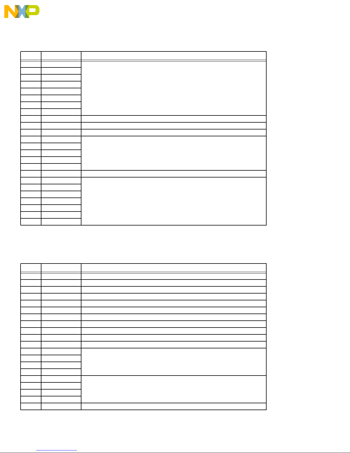
Table 8: P1 PORT C (D row)
D
D12 PC20
MIITXCLK(clock12)/ATM8-TxClk
D13 PC19
TDMA2-/RXCLK(clock13)/MIIRXCLK
D14 PC18
TDMA2-TXCLK(clock14)/MIITXCLK
D15 PC17
MIIRXCLK(clock15)/TDMB2-RXCLK
D16 PC16
MIITXCLK(clock16)/TDMB2-TXCLK
D17 NC
D18 NC
D19 PC13 PC13 is used to select one of the DS3 _1 Loopback.
D20 NC
D21 PC11
DS3-TXD3
D22 PC10
MIIMDC
D23 PC9
MIIMDIO
D24 NC
D25 NC
D26 NC
D27 NC
D28 NC
D29 NC
D30 NC
D31 NC
D32 NC
FE_1 MIITXCLK signal on FCC1 or ATM8 TxClk signal on ADS.
T1_5 RXCLK signal or FE_0 MIIRXCLK signal on ADS.
T1_5 TXCLK signal or FE_0 MIITXCLK signal on ADS.
T1_6 RXCLK signal or FE_2 MIIRXCLK signal on FCC3
T1_6 TXCLK signal or FE_2 MIITXCLK signal on FCC3
DS3_2 RT will be low if PC13 and PA1 will be low.
DS3_2 TR will be low if PC13 will be high and PA1 will be low.
DS3_2 TXD3 signal on FCC3
FE_(0,1,2) MIIMDC signal. The MDC signal is a GPIO that the user should configure for this
purpose. The TCOM SW has a program for this configuration. The PMC8260 dose not have a
special pin for MDC.
FE_(0,1,2) MIIMDIO signal. The MDIO signal is a GPIO that the user should configure for this
purpose. The TCOM SW has a program for this configuration. The PMC8260 dose not have a
special pin for MDIO.
4•2•2 P2 ADDRESS, DATA CONTROL and STATUS signals.
eescale S
Fr
A
A1 NC
A2 VA17 Not Used.
A3 VA18 PM4388 TOCTL (T1_1 - T1_8 FRAMER) CS signal uses !A20 & !A19 & !A18 & !BRDCS1 (CS6).
A4 VA19
A5 VA20
A6 VA21 A21 is the MSB of the TOCTL device address bus. (PM4388).
A7 VA22 A22 is one of the address bus signals of the TOCTL (PM4388).
A8 VA23 A23 of the address bus of the TOCTL and 2 QDSX (T1 LIU).
Table 9: P2 ADD and Power (A row)
PM4314 QDSX (T1_1 - T1_4 LIU) CS signal uses !A20 & !A19 & A18 & !BRDCS1 (CS6),
PM4314 QDSX (T1_5 - T1_8 LIU) CS signal uses !A20 & A19 & !A18 & !BRDCS1 (CS6),
TXC-03401 DS3F ( DS3_1) CS signal uses !A20 & A19 & A18 & !BRDCS1 (CS6).
TXC-03401 DS3F (DS3_2) CS signal uses A20 & !A19 & !A18 & !BRDCS1 (CS6).
For More Information On This Product,
Go to: www.freescale.com
39
Page 40
MPC8260TCOM User’s Manual PRELIMINARY
Freescale Semiconductor, Inc.
SUPPORT INFORMATION
Table 9: P2 ADD and Power (A row)
A
A9 VA24 The address bus of the TOCTL, 2 QDSX (T1 LIU) and 2 DS3F FRAMER.
A10 VA25
A11 VA26
A12 VA27
A13 VA28
A14 VA29
A15 VA30
A16 VA31
A17 NC
A18 NC
A19 NC
A20 3.3V 3.3V POWER SUPPLY FOR THE TCOM BOARD FROM THE ADS.
A21 3.3V
A22 3.3V
A23 3.3V
nc...
A24 3.3V
A25 NC
, I
A26 5V VCC 5V POWER SUPPLY FOR THE TCOM BOARD FROM THE ADS.
or
A27 5V VCC
A28 5V VCC
A29 5V VCC
A30 5V VCC
A31 5V VCC
A32 5V VCC
emiconduct
Table 10: TCOM STATUS (B row)
B
B1 GND
B2 GND
B3 GND
B4 DS3_TR1 If this signal is low the DS3_1 is in TR loopback. It can be read through the ADS BCSR2.
B5 DS3_RT1 If this signal is low the DS3_1 is in RT loopback. It can be read through the ADS BCSR2.
eescale S
B6 DS3_TR2 If this signal is low the DS3_2 is in TR loopback. It can be read through the ADS BCSR2.
B7 DS3_RT2 If this signal is low the DS3_2 is in RT loopback. It can be read through the ADS BCSR2.
Fr
B8 ENDS3_1 If this signal is low the DS3_1 is enable. It can be read through the ADS BCSR2.
B9 ENDS3_2 If this signal is low the DS3_2 is enable. It can be read through the ADS BCSR2.
B10 NC
B11 NC
B12 TOOLREV0 These 4 signals indicate through the BCSR2 on the ADS what is the rev of the 8260TCOM board
B13 TOOLREV1
B14 TOOLREV2
B15 TOOLREV3
B16 TOOLTYP0 These 4 signals indicate through the BCSR2 on the ADS what type of the board is connected to the
B17 TOOLTYP1
B18 TOOLTYP2
B19 TOOLTYP3
B20 NC
connected to the ADS
ADS
40
For More Information On This Product,
Go to: www.freescale.com
Page 41
PRELIMINARY MPC8260TCOM User’s Manual
Freescale Semiconductor, Inc.
SUPPORT INFORMATION
Table 10: TCOM STATUS (B row)
B
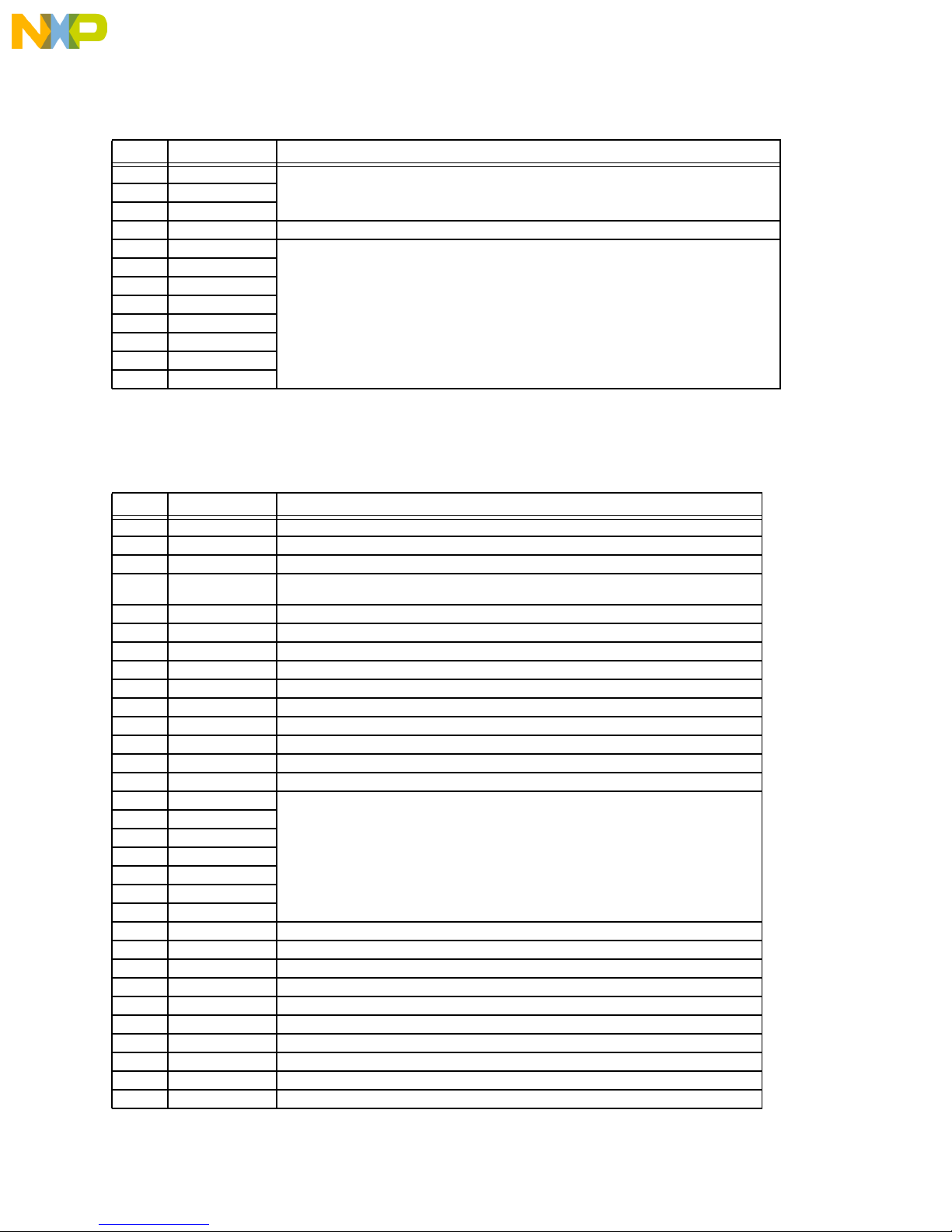
B21 3.3V POWER 3.3V supply to the TCOM from the ADS.
B22 3.3V
B23 3.3V
B24 NC
B25 VCC 5V POWER 5V supply to the TCOM from the ADS.
B26 VCC 5V
B27 VCC 5V
B28 VCC 5V
B29 VCC 5V
B30 VCC 5V
B31 VCC 5V
B32 VCC 5V
nc...
, I
or
emiconduct
eescale S
Fr
Table 11: DATA and Control signals. (C row)
C
C1 GND
C2 CLK8
C3 GND
C4 BRDCS1~ MPC8260 CS6 signal use together with A18,A19 and A20 to select one of the devices on the
TCOM
C5 BRDCS2~ not used
C6 GND
C7 ADSATMEN ADS ATM8 enable signal not used on the TCOM.
C8 NC
C9 NC
C10 RESET~ MPC8260 HRESET signal.
C11 NC
C12 INT~ MPC8260 INT7~ signal
C13 GND
C14 VD0
C15 VD1 MPC8260 D0-D7 data bus. use as a data for the TOCTL,QDSX,DS3F devices.
C16 VD2
C17 VD3
C18 VD4
C19 VD5
C20 VD6
C21 VD7
C22 NC
C23 NC
C24 NC
C25 NC
C26 NC
C27 NC
C28 NC
C29 NC
C30 NC
C31 NC
For More Information On This Product,
Go to: www.freescale.com
41
Page 42
MPC8260TCOM User’s Manual PRELIMINARY
Freescale Semiconductor, Inc.
SUPPORT INFORMATION
Table 11: DATA and Control signals. (C row)
C
C32 NC
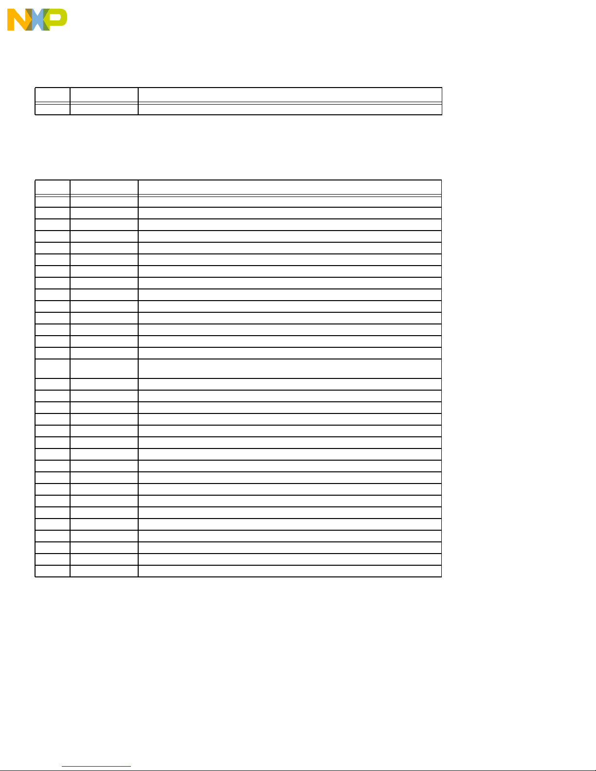
Table 12: Control Signals. (D row)
D
D1 GND
D2 GND
D3 GND
D4 WE0~ MPC8260 WE0~ signal. Not used
D5 WE1~ MPC8260 WE0~ signal. Not used
D6 GND
D7 GPL0~ MPC8260 GPL0~ signal. Used as an ALE signal for the DS3F.
nc...
D8 GPL1~ MPC8260 GPL1~ signal used as an ADDRESS buffer or for the DS3F.
D9 GPL2~ MPC8260 GPL2~ signal used as a read signal on the TCOM board.
, I
D10 GPL3~ MPC8260 GPL3~ signal used as a write signal on the TCOM board.
or
D11 GPL4~ MPC8260 GPL4~ signal used as a DS3F buffer OE~ signal.
D12 GPL5~ MPC8260 GPL5~ signal not used.
D13 GND
D14 ALE MPC8280 ALE signal not used.
D15 BCTL0 MPC8260 BCTL0 signal used as a read/write signal. In the TCOM it is a direction signal for the
D16 GND
D17 GND
D18 GND
D19 GND
emiconduct
D20 GND
D21 GND
D22 GND
D23 GND
D24 GND
D25 GND
D26 GND
D27 GND
eescale S
D28 GND
D29 GND
Fr
D30 GND
D31 GND
D32 GND
data of the DS3F for the DS3_1 and DS3_2.
42
For More Information On This Product,
Go to: www.freescale.com
Page 43
PRELIMINARY MPC8260TCOM User’s Manual
Freescale Semiconductor, Inc.
SUPPORT INFORMATION
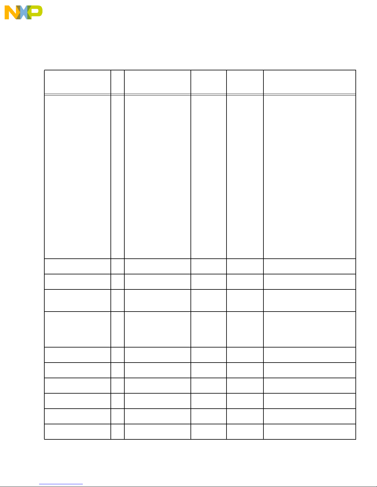
Table 5-1 MPC8260TCOM Parts List
Table 6:
nc...
, I
or
emiconduct
eescale S
Fr
DESCRIPTION
100NF 16V 10% X7R
0603 SMD
100UF/10V TNT D SMT
10%
22uF 25V/10% SIZE D
T/R SMD
10NF 50V 10% SMD
1206
10UF 25v 10% C TNT
SMD
18PF 5% 50V COG
1206 SMD
0.047UF (47nf) 50V
10% 12
0.47UF 50V 1812 SMD 8. 1812 5C 474K ATJ AVX 021-00113 C86 C93 C96 C103 C108 C113
1nF 2KV X7R 1210
SMD CERRAMIC
0.68uF 50V SMD X7R
1812 T
1000P (1nF) 50V 10%
1206
Q
U
1
3
4
4 B45196-H2107K SIEMENS 023-00038 C2 C3 C5 C6
1 TAJD226K025R AVX 023-00048 C16
171206 5C 103K ATJ AVX 021-00070 C17 C18 C30 C36 C43 C51 C61
26B45196-H5106-K309 SIEMENS 023-00027 C26 C27 C41 C44 C45 C49 C52
4 12065A180JAT AVX 021-00128 C47 C48 C55 C56
8. AV12065C473KATJ AVX 021-00095 C73 C74 C81 C82 C134 C137
2 1210B102K202NT AVX 021-00126 C152 C153
8 18125C684KAT2A AVX 021-00138 C154 C155 C156 C157 C158
8. AVX12065C102KA AVX 021-00105 C168,C171,C173,C175
MANUFACTURER
PART NUMBER
B37931K9104K60 SIEMENS 021-00118 C1 C4 C7 C8 C9 C10 C11 C12
MANUFAC
TURER
MOT.
PART
NUMBER
LOCATION
C13 C14 C15 C19 C20 C21 C22
C23 C24 C25 C28 C29 C31 C32
C33 C34 C35 C37 C38 C39 C40
C42 C46 C50 C54 C57 C58 C60
C66 C71 C72 C75 C76 C77 C78
C79 C80 C85 C87 C88 C89 C90
C91 C92 C94 C95 C97 C98 C99
C100 C101 C102 C104 C105
C106 C107 C109 C110 C111
C112 C114 C115 C117 C118
C119 C120 C122 C123 C124
C125 C126 C127 C132 C133
C135 C136 C138 C139 C140
C141 C142 C144 C145 C146
C147 C148 C162 C163 C165
C166 C167 C169 C170 C172
C174 C177 C178 C180 C182
C184 C185 C186 C187 C188
C189 C190 C193 C194 C195
C196 C197 C198 C199 C200
C201 C202 C204 C209 C213
C214 C215 C216 C217 C218
C219 C220
C62 C63 C67 C68 C69 C83 C84
C164 C191 C192
C53 C59 C64 C65 C70 C128
C129 C130 C131 C150 C151
C203 C205 C206 C207 C208
C210 C211 C212
C143 C149
C116 C121
C159 C160 C161
C176,C179,C181,C183.
For More Information On This Product,
Go to: www.freescale.com
43
Page 44
MPC8260TCOM User’s Manual PRELIMINARY
Freescale Semiconductor, Inc.
SUPPORT INFORMATION
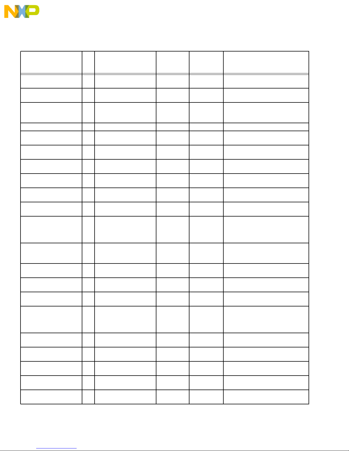
Table 6:
DESCRIPTION
GND BRIDGE 2.54MM
GOLD
Impedance 45-95 SMD
FERRIT
GREEN LED SMD 18LG-T670-HK SIEMENS 048-01001 LD1 LD2 LD3 LD4 LD5 LD6 LD8
RED LED SMD 6 LS-T670-HK SIEMENS 048-01002 LD7 LD10 LD11 LD12 LD14 LD15
128 PIN MALE PC 90'
DIN C
10PIN TERM STRIP
SHORT SMD
nc...
2 PORT SHILDED 90'
MODULA
, I
BNC FEM STRGHT
FOR PC
or
8 PORT SHILDED 90'
MODULA
0 OHM 1% 1/4W 1206
SMD
390 ohm 1% 0603 SMD
T/R
22 OHM 5%1/8W 1206
emiconduct
SMD
54.9 OHM 1% 1206
SMD T/R
12 OHM 1% 1206 SMD
T/R
33.2 1% 1/8W 1206
SMD
eescale S
4.7K 1% 1206 SMD 21D25 04K7FCS ROEDERS
Q
U
7 PD 999 11 11010 PRECIDIP 022-00012 J1 J2 J3 J4 J5 J6 J7
362743021447 FAIR RITE 024-00013 L1-L36
2 023816 ERNI 028-00279 P1 P2
1 TSM10501-SDV AP SAMTEC 028-00171 P3
1. 43223-8128 MOLEX 009-00435 P4
4073133-5003 MOLEX 009-00226 P5 P6 P7 P8
1. 43223-8182 MOLEX 009-00436 P9
9 D25 000RFCS ROEDERS
16CR0603 390RF DRALORIK006-00384 R1 R2 R3 R4 R5 R6 R9 R15 R16
15D25 022 RJSC ROEDERS
5. D25 54R9FCS ROEDERS
1. D25 012RFCS ROEDERS
2 D25 33R2FCS ROEDERS
Fr
1K 1% 1/4W METAL
1206
36 ohm 5% 1206 SMD
T/R
100 OHM 1% 1/4W
1206
22.1K 1% 1/4W SMD
1206
316K 1% 1206 SMD T/R8. D25 316KFCS ROEDERS
6 D25001KFCS DRALORIK006-00257 R29 R30 R34 R35 R42 R43
2 D25 036RFCS DRALORIK006-00398 R36 R44.
2 D25-100RFCS ROEDERS
2 D25-22K1FCS DRALORIK006-00236 R52 R54
MANUFACTURER
PART NUMBER
MANUFAC
TURER
TEIN
TEIN
TEIN
TEIN
TEIN
TEIN
TEIN
TEIN
MOT.
PART
NUMBER
LD9 LD13 LD16 LD17 LD18 LD19
LD20 LD21 LD22 LD23 LD24
006-00252 R0 R97 R99 R101 R102 R103
R105 R107 R108
R17 R19 R20 R23 R24 R25 R26
RT1 RT2 RT3 RT4 RT5 RT6 RT7
RT8 R130 R131
006-00301 R7 R10 R18 R21 R22 R38 R40
R41 R68 R115 R116 R117 R119
R121 R122 R123 R125
006-00354 R8 R11 R12 R13 R31.
006-00355 R14
006-00286 R27 R32.
006-00321 R28 R33 R37 R39 R45 R46 R47
R48 R49 R50 R55 R64 R65 R66
R67 R109 R111 R112 R113 R126
R127.
006-00240 R51 R53
006-00353 R56 R57 R62 R63 R73 R76 R77
R80
LOCATION
44
For More Information On This Product,
Go to: www.freescale.com
Page 45
PRELIMINARY MPC8260TCOM User’s Manual
Freescale Semiconductor, Inc.
SUPPORT INFORMATION
Table 6:
nc...
, I
or
emiconduct
eescale S
Fr
DESCRIPTION
93.1 OHM 1% 1206
SMD T/R
R 49,9 OHM 1% SMD
1206
75 OHM 5%1/4W MTL
1206
309 OHM 1% 1206
SMD T/R
51.1 1% 1/4W 1206
SMD
191 OHM 1% 1206
SMD T/R
RES 330 OHM SMD
5% 1206
0ohm 5% 4R 8P SMD
CHIP R
51ohm 5% 4R 8P SMD
CHIP R
22ohm 5% 4R 8P SMD
CHIP R
4.7K 13R 14P SMD T/R 1 SOMC1401472 DALE 051-00036 RN16
10K 5% 14P 13R SMD
T/R
ETHERNET
TRANSCEIVER LXT9
MC74LCX541DW SMD 11MC74LCX541DW MOTOROLA051-
OCTAL T1 FRAMER
PM4388-R1
16.384MHz 3.3V 4P
CRYS OS
12.352MHz 3.3V 4P
CRYS OS
TRANSFORMETR
TG22-3506
DS3 FRAMER TXC03401B
QUAD T1/E1
INTRFACE PM431
44.736MHz 5V 8P
CRYS OSC.
Q
U
8. D25 93R1FCS ROEDERS
16D25 49R9FCS ROEDERS
8 D25 075RJCS ROEDERS
8. D25 309RFCS ROEDERS
3 D25 51R1FCS ROEDERS
22D25 191RFCS ROEDERS
2 D25 330RJCS
10CRA06S0803 000 RT DALE 051-00067 RN1 RN2
10CRA06S0803510JR DALE 051-00070 RN3 RN4 RN5 RN6 RN7
10CRA06S0803220JR DALE 051-00068 RN8 RN9 RN10 RN11 RN12
1 SOMC 1401103J TR DALE 051-00046 RN17
2 LXT970QC LEVEL
1 PM4388-RI PMC
1 M3H16FCD 048-00103 U9 for E1
1 M3H16FCD 048-00104 U9 for T1
2 TG22-3506ND HALO 091-TG22-
2 TXC-03401B TRANSWI
2 PM4314-RI PMC
1 MH16FDD 048-00105 U16
MANUFACTURER
PART NUMBER
MANUFAC
TURER
TEIN
TEIN
TEIN
TEIN
TEIN
TEIN
ROEDERS
TEIN
ONE
SIERA
TCH
SIERA
MOT.
PART
NUMBER
006-00352 R58 R59 R60 R61 R74 R75 R78
R79
006-00192 R69 R70 R71 R72 R85 R86 R87
R88 R89 R90 R91 R92 R93 R94
R95 R96
006-00260 R81 R82 R83 R84 R156 R157
R158 R159
006-00351 R98 R100 R104 R106 R114 R118
R120 R124.
006-00221 R110 R128 R129
006-00344 R132 R133 R134 R135 R136
R137 R138 R139 R140 R141
R142 R143 R144 R145 R147
R148 R150 R151 R152 R153
R154 R155
006-00191 R146 R149
RN13 RN14 RN15
051LXT970QC
74LCX541
DW
051PM4388-RI
3506ND
051-
TXC03401
B
051PM4314-RI
U1 U2
U3 U4 U5 U6 U7 U25 U26 U27
U28 U29 U31
U8
U10 U11
U12 U13
U14 U15
LOCATION
For More Information On This Product,
Go to: www.freescale.com
45
Page 46
MPC8260TCOM User’s Manual PRELIMINARY
Freescale Semiconductor, Inc.
SUPPORT INFORMATION
Table 6:
DESCRIPTION
MACH221SP-15YC 1 MACH221SP-7YC AMD 051-
MC74LCX245DW SMD 1 MC74LCX245DW MOTOROLA051-
T1/E1/CEPT QUAD
PORT TRANFORMER
LINE INTRFACE
MODULE TXC-20153G
PLL MPC931FA 1 MPC931FA MOTOROLA051-
Q
U
2 ST5170T VALOR 051-
2 TXC-20153G TRANSWI
nc...
74ACT161D SMD 1 MC74ACT161D MOTOROLA051-
, I
or
74ACT244DW SMD 1 74ACT244DW MOTOROLA051-
14 PIN SMD SOCKET
G/T
Crystal 25MHz 2 MA505 +/-50PPM
RUBBER LEGS 7 SJ5018 BLACK 3M 107-01325
2 110-91-314-41-105 PRECIDIP 009-00262
MANUFACTURER
PART NUMBER
25MHz
MANUFAC
TURER
MACH221S
P-15
74LCX245
D
ST5170T
051-
TCH
EPSON 048-00099 Y1-Y2
TXC20153
G
MPC931FA
74ACT161
D
74ACT244
D
emiconduct
4•2•3 MPC8260TCOM nettlist
/8XT1E1PL R44(2) U24(2);
/8XT1_E1 I3(1) U8(123) U23(15);
/ADSATMEN P2(C7) U17(97);
eescale S
Fr
/ALE P2(D14) RT6(1) U17(8);
/BCTL0 P2(D15) RT7(1) U17(4);
/BQ1TCLK1 R17(1) U8(10) U14(78) U26(5);
/BQ1TCLK2 R16(1) U7(5) U8(12) U14(75);
/BQ1TCLK3 R20(1) U6(5) U8(14) U14(72);
/BQ1TCLK4 R24(1) U8(16) U14(69) U27(5);
/BQ2TCLK5 R23(1) U4(5) U8(23) U15(78);
/BQ2TCLK6 R26(1) U3(5) U8(25) U15(75);
/BQ2TCLK7 R15(1) U8(27) U15(72) U25(5);
/BQ2TCLK8 R19(1) U5(5) U8(29) U15(69);
/BRDCS1~ P2(C4) RT4(1) U17(22);
/BRDCS2~ P2(C5) RT8(2) U17(26);
/BRICLK1 R3(1) U8(96) U26(2);
/BRICLK2 R9(1) U7(2) U8(91);
/BRICLK3 R2(1) U6(2) U8(88);
/BRICLK4 R5(1) U8(83) U27(2);
MOT.
PART
NUMBER
U17
U18
U19 U20
U21 U22
U23
U24
U30
LOCATION
46
For More Information On This Product,
Go to: www.freescale.com
Page 47

nc...
, I
or
emiconduct
eescale S
Fr
PRELIMINARY MPC8260TCOM User’s Manual
Freescale Semiconductor, Inc.
SUPPORT INFORMATION
/BRICLK6 R25(1) U3(2) U8(77);
/BRICLK7 R1(1) U8(72) U25(2);
/BRICLK8 R4(1) U5(2) U8(69);
/BRID1 U8(97) U26(4);
/BRID2 U7(4) U8(94);
/BRID3 U6(4) U8(89);
/BRID4 U8(84) U27(4);
/BRID5 U4(4) U8(81);
/BRID6 U3(4) U8(78);
/BRID7 U8(73) U25(4);
/BRID8 U5(4) U8(70);
/BRIFP1 U8(95) U26(3);
/BRIFP2 U7(3) U8(90);
/BRIFP3 U6(3) U8(87);
/BRIFP4 U8(82) U27(3);
/BRIFP5 U4(3) U8(79);
/BRIFP6 U3(3) U8(76);
/BRIFP7 U8(71) U25(3);
/BRIFP8 U5(3) U8(68);
/BTED1 U8(115) U26(13);
/BTED2 U7(13) U8(113)
/BTED3 U6(13) U8(111);
/BTED4 U8(109) U27(13)
/BTED5 U4(13) U8(105);
/BTED6 U3(13) U8(103);
/BTED7 U8(101) U25(13);
/BTED8 U5(13) U8(99);
/BTEFP1 U8(114) U26(6);
/BTEFP2 U7(6) U8(112)
/BTEFP3 U6(6) U8(110);
/BTEFP4 U8(106) U27(6)
/BTEFP5 U4(6) U8(104);
/BTEFP6 U3(6) U8(102)
/BTEFP7 U8(100) U25(6);
/BTEFP8 U5(6) U8(98);
/CLK8 P2(C2) RT5(2) U17(13);
/DIRDS3DT U17(88) U18(1);
/DS3CLK1 I19(1) I35(1) R130(1) U13(62) U13(52) U22(27) U30(18);
/DS3CLK2 I43(1) I54(1) R131(1) U12(52) U12(62) U21(27) U30(16);
/DS3F1CS~ I20(1) R49(2) U13(8) U17(69);
/DS3F2CS~ I44(1) R50(2) U12(8) U17(70);
/DS3F_AD0 I34(1) U12(18) U13(18) U18(9) U31(11);
/DS3F_AD1 I33(1) U12(19) U13(19) U18(8) U31(12);
/DS3F_AD2 I32(1) U12(20) U13(20) U18(7) U31(13);
/DS3F_AD3 I31(1) U12(21) U13(21) U18(6) U31(14)
/DS3F_AD4 I30(1) U12(23) U13(23) U18(5) U31(15);
/DS3F_AD5 I29(1) U12(24) U13(24) U18(4) U31(16);
/DS3F_AD6 I28(1) U12(25) U13(25) U18(3) U31(17);
/DS3F_AD7 I27(1) U12(26) U13(26) U18(2) U31(18);
/DS3RC1 U13(5) U22(33);
/DS3RC2 U12(5) U21(33)
/DS3RCLK1 RN15(5) U26(18) U28(14);
/DS3RCLK2 RN14(8) U6(18) U29(14)
/DS3RD0_1 RN13(8) U26(16) U28(15);
For More Information On This Product,
Go to: www.freescale.com
47
Page 48

MPC8260TCOM User’s Manual PRELIMINARY
Freescale Semiconductor, Inc.
SUPPORT INFORMATION
/DS3RD1 U13(29) U22(29)
/DS3RD1_1 RN13(7) U5(16) U28(16);
/DS3RD1_2 RN14(7) U5(18) U29(16)
/DS3RD2 U12(29) U21(29);
/DS3RD2_1 RN13(6) U5(7) U28(17)
/DS3RD2_2 RN14(6) U29(17);
/DS3RD3_1 RN13(5) U25(17) U28(18)
/DS3RD3_2 RN14(5) U29(18);
/DS3RSYN1 RN15(6) U26(17) U28(13);
/DS3TC1 U13(1) U22(21);
/DS3TC2 U12(1) U21(21)
/DS3TCK_1 RN15(7) U5(15) U28(12);
/DS3TCK_2 R68(2) U6(15) U29(12)
/DS3TD1 U13(3) U22(23);
/DS3TD1_1 RN12(3) U5(17) U13(59)
/DS3TD2 U12(3) U21(23);
/DS3TD2_1 RN12(2) U5(14) U13(58)
nc...
, I
or
emiconduct
eescale S
Fr
/DS3TD3_1 I39(1) RN12(8) U13(56) U25(14);
/DS3TSYN1 RN15(8) U26(14) U28(11);
/DS3_RT1~ P2(B5) RN17(6) U17(82) U22(16);
/DS3_RT2~ P2(B7) RN17(10) U17(85) U21(16);
/DS3_TR1~ P2(B4) RN17(5) U17(84) U22(17);
/DS3_TR2~ P2(B6) RN17(9) U17(86) U21(17);
/ENDS3_1 P2(B8) R113(2) R144(1) U17(49) U28(1) U28(19);
/ENDS3_2 P2(B9) R55(2) R147(1) U17(47) U29(1) U29(19);
/EN_T1_1 P1(A28) R136(1) RN16(2) U17(45) U26(19) U26(1);
/EN_T1_2 LD23(1) P1(A27) RN16(12) U7(1) U7(19) U17(44);
/EN_T1_3 P1(A26) R138(1) RN16(3) U6(1) U6(19) U17(43);
/EN_T1_4 LD21(1) P1(A25) RN16(11) U17(38) U27(19) U27(1);
/EN_T1_5 P1(A24) R140(1) RN16(4) U4(19) U4(1) U17(37);
/EN_T1_6 LD19(1) P1(A23) RN16(5) U3(19) U3(1) U17(36);
/EN_T1_7 LD18(1) P1(A14) RN16(6) U17(35) U25(1) U25(19);
/EN_T1_8 P1(A13) R143(1) RN16(7) U5(19) U5(1) U17(34);
/FECOL_1 RN7(7) U1(64)
/FECOL_2 RN5(7) U2(64);
/FECRS_1 RN7(8) U1(1)
/FECRS_2 RN5(8) U2(1);
/FERXCLK1 I10(1) R13(1) U1(54)
/FERXCLK2 I12(1) R11(1) U2(54);
/FERXD0_1 RN6(8) U1(50)
/FERXD0_2 RN4(5) U2(50);
/FERXD1_1 RN6(7) U1(49)
/FERXD1_2 RN4(6) U2(49);
/FERXD2_1 RN6(6) U1(48)
/FERXD2_2 RN4(7) U2(48);
/FERXD3_1 RN6(5) U1(47)
/FERXD3_2 RN4(8) U2(47) U27(7);
/FERX_DV1 RN7(5) U1(51);
/FERX_DV2 RN5(5) U2(51);
/FERX_ER1 RN7(6) U1(55)
/FERX_ER2 RN5(6) U2(55);
/FETXCLK1 I9(1) R32(1) U1(57)
/FETXCLK2 I11(1) R27(1) U2(57);
/FETXD0_2 RN3(8) U2(59) U4(7) U12(60);
48
For More Information On This Product,
Go to: www.freescale.com
Page 49

nc...
, I
or
emiconduct
eescale S
Fr
PRELIMINARY MPC8260TCOM User’s Manual
Freescale Semiconductor, Inc.
SUPPORT INFORMATION
/FETXD1_2 RN3(7) U2(60) U4(16) U29(15);
/FETXD2_2 RN3(6) U2(61) U4(14) U29(11);
/FETXD3_2 RN3(5) U2(62) U4(17) U29(13);
/FETXD4_1 R33(2) U1(63);
/FETXD4_2 R28(2) U2(63);
/FETX_EN2 R8(1) U2(58) U6(16)
/FE_MDIO R31(1) U1(44);
/GPL0~ I23(1) I47(1) P2(D7) U12(10) U13(10)
/GPL1~ P2(D8) U31(1) U31(19);
/GPL2~ I21(1) I45(1) P2(D9) U8(67) U12(12) U13(12) U14(11) U15(11);
/GPL3~ I22(1) I46(1) P2(D10) U8(66) U12(14) U13(14) U14(10) U15(10);
/GPL4~ P2(D11) U17(75) U18(19)
/GPL5~ P2(D12) U17(73);
/INT~ P2(C12) R12(2) R37(2) U1(2) U8(40) U14(12) U15(12) U17(87);
/MCHINT~ U12(15) U13(15) U17(9)
/PA1 P1(B31) RN16(8) U17(32);
/PA2 P1(B30) RN15(2);
/PA3 P1(B29) RN14(2);
/PA5 P1(B27) R126(1) U17(23);
/PA6 P1(B26) RN15(3);
/PA7 P1(B25) RN15(1);
/PA8 P1(B24) RN13(1);
/PA9 P1(B23) U13(60) U26(7);
/PA14 P1(B18) RN6(4);
/PA15 P1(B17) RN6(3);
/PA16 P1(B16) RN6(2);
/PA17 P1(B15) RN6(1);
/PA18 P1(B14) U1(59);
/PA19 P1(B13) U1(60);
/PA20 P1(B12) U1(61);
/PA21 P1(B11) U1(62);
/PA26 P1(B6) RN7(3);
/PA27 P1(B5) RN7(4);
/PA28 P1(B4) U1(58);
/PA29 P1(B3) U1(56);
/PA30 P1(B2) RN7(1);
/PA31 P1(B1) RN7(2);
/PB4 P1(C28) RN3(4);
/PB5 P1(C27) RN3(3);
/PB6 P1(C26) RN3(2);
/PB7 P1(C25) RN3(1);
/PB8 P1(C24) RN4(4) RN10(3);
/PB9 P1(C23) R41(1) RN4(3) U12(58);
/PB10 P1(C22) RN4(2) RN10(2);
/PB11 P1(C21) RN4(1);
/PB12 P1(C20) R10(1) RN5(1);
/PB13 P1(C19) R40(1) RN5(2) U12(59);
/PB14 P1(C18) R8(2);
/PB15 P1(C17) U2(56) U6(7);
/PB16 P1(C16) RN5(3);
/PB17 P1(C15) RN5(4);
/PB18 P1(C14) RN14(3);
/PB19 P1(C13) RN14(4);
/PB20 P1(C12) RN12(6);
For More Information On This Product,
Go to: www.freescale.com
49
Page 50

MPC8260TCOM User’s Manual PRELIMINARY
Freescale Semiconductor, Inc.
SUPPORT INFORMATION
/PB21 P1(C11) RN12(7);
/PB22 P1(C10) RN13(2);
/PB23 P1(C9) RN13(3);
/PB24 P1(C8) RN13(4);
/PB25 P1(C7) RN12(1);
/PB26 P1(C6) RN9(3);
/PB27 P1(C5) U25(7);
/PB28 P1(C4) RN11(1);
/PB29 P1(C3) RN11(4);
/PB30 P1(C2) RN11(3);
/PB31 P1(C1) U3(7);
/PC9 P1(D23) R31(2) U2(44);
/PC10 P1(D22) U1(45) U2(45);
/PC11 I68(1) P1(D21) U12(56);
/PC13 P1(D19) R127(1) U17(25);
/PC16 P1(D16) R27(2) RN11(2);
/PC17 P1(D15) R7(1) R11(2);
nc...
, I
or
emiconduct
eescale S
Fr
/PC18 P1(D14) R22(2);
/PC19 P1(D13) R18(1);
/PC20 P1(D12) R32(2);
/PC21 P1(D11) R13(2);
/PC22 P1(D10) RN8(1);
/PC23 P1(D9) RN8(4);
/PC24 P1(D8) RN10(1);
/PC25 P1(D7) RN10(4);
/PC26 P1(D6) R68(1);
/PC27 P1(D5) RN14(1);
/PC28 P1(D4) RN9(2);
/PC29 P1(D3) RN9(4);
/PC30 P1(D2) R21(1);
/PC31 P1(D1) RN15(4);
/PD10 P1(A22) RN8(3);
/PD11 P1(A21) R38(1);
/PD12 P1(A20) RN8(2);
/PD13 P1(A19) U7(7);
/Q1RCLK1 U8(2) U14(98);
/Q1RCLK2 U8(4) U14(95);
/Q1RCLK3 U8(6) U14(90);
/Q1RCLK4 U8(8) U14(87);
/Q1RXD1 U8(1) U14(100);
/Q1RXD2 U8(3) U14(97);
/Q1RXD3 U8(5) U14(92);
/Q1RXD4 U8(7) U14(89);
/Q1TXD1 U8(9) U14(77);
/Q1TXD2 U8(11) U14(74);
/Q1TXD3 U8(13) U14(71);
/Q1TXD4 U8(15) U14(68);
/Q1XCLKO I7(1) U14(86);
/Q2RCLK5 U8(32) U15(98);
/Q2RCLK6 U8(34) U15(95);
/Q2RCLK7 U8(36) U15(90);
/Q2RCLK8 U8(38) U15(87);
/Q2RXD5 U8(31) U15(100);
/Q2RXD6 U8(33) U15(97);
50
For More Information On This Product,
Go to: www.freescale.com
Page 51

nc...
, I
or
emiconduct
eescale S
Fr
PRELIMINARY MPC8260TCOM User’s Manual
Freescale Semiconductor, Inc.
SUPPORT INFORMATION
/Q2RXD7 U8(35) U15(92);
/Q2RXD8 U8(37) U15(89);
/Q2TXD5 U8(22) U15(77);
/Q2TXD6 U8(24) U15(74);
/Q2TXD7 U8(26) U15(71);
/Q2TXD8 U8(28) U15(68);
/Q2XCLKO I8(1) U15(86);
/QDSX1CLK U14(79) U23(27);
/QDSX1CS~ R109(2) U14(9) U17(61);
/QDSX2CLK U15(79) U23(26);
/QDSX2CS~ R111(2) U15(9) U17(62);
/RBNC1N P7(2) R157(2) U22(49);
/RBNC1P P7(1) R157(1) U22(50);
/RBNC2N P5(2) R159(2) U21(49);
/RBNC2P P5(1) R159(1) U21(50);
/RESET~ P2(C10) RT3(2) U17(54);
/RN6R8 I53(1) R67(2) U12(49);
/RN6R9 I67(1) R66(2) U12(50);
/RSTBRD~ R45(2) U1(16) U2(16) U8(125) U8(39) U14(5) U14(7) U15(7) U15(5) U17(72);
/RXRING1 C177(1) R79(2) U14(127) U19(23);
/RXRING2 C178(1) R61(2) U14(104) U19(28);
/RXRING3 C180(1) R78(2) U14(40) U19(33);
/RXRING4 C182(1) R60(2) U14(63) U19(38);
/RXRING5 C169(1) R75(2) U15(127) U20(23);
/RXRING6 C170(1) R59(2) U15(104) U20(28);
/RXRING7 C172(1) R74(2) U15(40) U20(33);
/RXRING8 C174(1) R58(2) U15(63) U20(38);
/RXTIP1 R79(1) R120(1) U14(128);
/RXTIP2 R61(1) R104(1) U14(103);
/RXTIP3 R78(1) R106(1) U14(39);
/RXTIP4 R60(1) R124(1) U14(64);
/RXTIP5 R75(1) R114(1) U15(128);
/RXTIP6 R59(1) R98(1) U15(103);
/RXTIP7 R74(1) R100(1) U15(39);
/RXTIP8 R58(1) R118(1) U15(64);
/S3RAIS1~ RN17(2) U22(31);
/S3RAIS2~ RN17(12) U21(31);
/S3TAIS1~ RN17(3) U22(30);
/S3TAIS2~ RN17(13) U21(30);
/T1_E1CLK I2(1) U8(120) U24(12);
/TBNC1N P8(2) R156(2) U22(1);
/TBNC1P P8(1) R156(1) U22(2);
/TBNC2N P6(2) R158(2) U21(1);
/TBNC2P P6(1) R158(1) U21(2);
/TFOUT1~ I16(1) U13(47);
/TOCTLCS~ RN16(1) U8(65) U17(60);
/TOOLREV0 P2(B12) RN2(1);
/TOOLREV1 P2(B13) RN2(2);
/TOOLREV2 P2(B14) RN2(3);
/TOOLREV3 P2(B15) RN2(4);
/TOOLTYP0 P2(B16) RN1(1);
/TOOLTYP1 P2(B17) RN1(2);
/TOOLTYP2 P2(B18) RN1(3);
/TOOLTYP3 P2(B19) RN1(4);
For More Information On This Product,
Go to: www.freescale.com
51
Page 52

MPC8260TCOM User’s Manual PRELIMINARY
Freescale Semiconductor, Inc.
SUPPORT INFORMATION
/TXRING1 R103(1) U14(121);
/TXRING2 R105(1) U14(110);
/TXRING3 R107(1) U14(46);
/TXRING4 R108(1) U14(57);
/TXRING5 R97(1) U15(121);
/TXRING6 R99(1) U15(110);
/TXRING7 R101(1) U15(46);
/TXRING8 R102(1) U15(57);
/TXTIP1 C158(2) U14(118);
/TXTIP2 C159(2) U14(113);
/TXTIP3 C160(2) U14(49);
/TXTIP4 C161(2) U14(54);
/TXTIP5 C154(2) U15(118);
/TXTIP6 C155(2) U15(113);
/TXTIP7 C156(2) U15(49);
/TXTIP8 C157(2) U15(54);
/VA17 P2(A2) U17(20);
nc...
, I
or
emiconduct
eescale S
Fr
/VA18 P2(A3) U17(19);
/VA19 P2(A4) U17(12);
/VA20 P2(A5) U17(11);
/VA21 P2(A6) U8(64);
/VA22 P2(A7) U8(63);
/VA23 P2(A8) U8(62) U14(35) U15(35);
/VA24 P2(A9) U8(61) U14(34) U15(34) U31(9);
/VA25 P2(A10) U8(60) U14(33) U15(33) U31(8);
/VA26 P2(A11) U8(59) U14(32) U15(32) U31(7);
/VA27 P2(A12) U8(58) U14(31) U15(31) U31(6);
/VA28 P2(A13) U8(57) U14(30) U15(30) U31(5);
/VA29 P2(A14) U8(56) U14(29) U15(29) U31(4);
/VA30 P2(A15) U8(55) U14(28) U15(28) U31(3);
/VA31 P2(A16) U8(54) U14(27) U15(27) U31(2);
/VD0 P2(C14) U8(48) U14(26) U15(26) U18(11);
/VD1 P2(C15) U8(47) U14(25) U15(25) U18(12);
/VD2 P2(C16) U8(46) U14(24) U15(24) U18(13);
/VD3 P2(C17) U8(45) U14(17) U15(17) U18(14);
/VD4 P2(C18) U8(44) U14(16) U15(16) U18(15);
/VD5 P2(C19) U8(43) U14(15) U15(15) U18(16);
/VD6 P2(C20) U8(42) U14(14) U15(14) U18(17);
/VD7 P2(C21) U8(41) U14(13) U15(13) U18(18);
/VDS3EN1~ P1(A7) RN16(10) U17(95);
/VDS3EN2~ P1(B28) RN16(9) U17(96);
/VMF2 R35(2) R43(1) U1(8);
/VMF3 R34(2) R35(1) U1(4);
/VRCLK2 RN8(5) U7(18);
/VRCLK4 RN10(5) U27(18);
/VRCLK5 R18(2) U4(18);
/VRCLK7 RN9(5) U25(18);
/VRSYNC2 RN8(6) U7(17);
/VRSYNC6 RN11(5) U3(17);
/VRXD2 RN8(7) U7(16);
/VRXD6 RN11(6) U3(16);
/VRXD7 RN9(6) U25(16);
/VTCLK1 R21(2) U26(15);
/VTCLK2 RN8(8) U7(15);
52
For More Information On This Product,
Go to: www.freescale.com
Page 53

PRELIMINARY MPC8260TCOM User’s Manual
/VTCLK4 RN10(8) U27(15);
/VTCLK5 R22(1) U4(15);
/VTCLK7 RN9(7) U25(15);
/VTSYNC2 R38(2) U7(14);
/VTSYNC6 RN11(8) U3(14);
/WE0~ P2(D4) RT1(1) U17(68);
/WE1~ P2(D5) RT2(2) U17(63);
/XSIG745 C59(1) C60(1) C61(1) L4(2) L6(2) L11(1) U2(24);
/XSIG763 C65(1) C66(1) C67(1) L1(2) L3(2) L8(1) U1(24);
Freescale Semiconductor, Inc.
SUPPORT INFORMATION
nc...
, I
or
emiconduct
eescale S
Fr
For More Information On This Product,
Go to: www.freescale.com
53
 Loading...