

Page 1
© 2015 Freescale Semiconductor, Inc. All rights reserved.
Freescale Semiconductor, Inc.
Document Number: MPC5748GEVBUG
User Guide
Rev. 0
,
MPC5748G EVB User Guide
By: Alasdair Robertson
Page 2

Contents
1. INTRODUCTION ................................................................................................................................................................................. 3
1.1. Peripheral Daughtercards ............................................................................................................................................................. 3
2. EVB FEATURES .................................................................................................................................................................................. 3
3. CONFIGURATION OVERVIEW ......................................................................................................................................................... 5
4. MCU DAUGHTERCARD INFORMATION ........................................................................................................................................ 6
4.1. Fitting a daughtercard .................................................................................................................................................................. 6
4.2. Removing a daughtercard ............................................................................................................................................................ 6
5. INITIAL CONFIGURATION ............................................................................................................................................................... 7
5.1. Power Supply Configuration ....................................................................................................................................................... 7
5.1.1. Power Supply Connectors (P21, P23) .................................................................................................................................... 7
5.1.2. Power Switch (SW5) .............................................................................................................................................................. 8
5.1.3. Regulator Power Jumper (J23) ............................................................................................................................................... 8
5.1.4. Power Status LED’s and Fuse ................................................................................................................................................ 8
5.1.5. MCU Power Supply Jumpers (J18, J19, J20, J21, J22, J23) .................................................................................................. 9
5.1.6. Daughtercard Power Jumpers (J3 to J11) ............................................................................................................................. 10
5.1.7. Peripheral Power Supply Jumpers (J24, J25) ....................................................................................................................... 11
5.1.8. EVB Voltage Regulators ...................................................................................................................................................... 11
5.2. Reset Control (J9, SW1) ............................................................................................................................................................ 13
Note that removing jumper J9 will mean that an external reset source will not reset the MCU. This will impact most debuggers
which will typically issue a reset before establishing a debug connection. .......................................................................................... 13
5.2.1. Reset LEDs ........................................................................................................................................................................... 13
5.3. MCU Clock Configuration ........................................................................................................................................................ 14
5.3.1. External Clock Input (P7) ..................................................................................................................................................... 15
5.3.2. MCU Clock Configuration (J1, J2 on Daughtercard) ........................................................................................................... 15
5.4. Debug Connectors (P8, P10) ..................................................................................................................................................... 16
5.4.1. Debug Connector Pinouts ..................................................................................................................................................... 16
6. COMMUNICATIONS & MEMORY INTERFACES: ........................................................................................................................ 17
6.1. CAN Interfaces (P14, P15, J14, J15) ......................................................................................................................................... 17
6.2. LIN Interfaces (P9, P11, J10, J12) ............................................................................................................................................. 18
6.3. USB RS232 Serial Interface (P17, J16) ..................................................................................................................................... 19
6.4. USB HOST / OTG Interfaces .................................................................................................................................................... 20
6.5. Ethernet (P6, J5, J6, J7, J8, R45, R80) ....................................................................................................................................... 20
6.6. FlexRay (P2, P3, J1, J2, J3, J4) .................................................................................................................................................. 22
6.7. SD Card Socket (P200) .............................................................................................................................................................. 23
7. AV INTERFACE CONNECTORS ...................................................................................................................................................... 23
7.1. SAI Audio Connectors (P24, P25) ............................................................................................................................................. 23
7.2. TWRPI Connectors (P26, P27) .................................................................................................................................................. 25
7.3. MLB Daughtercard Connector (P16) ......................................................................................................................................... 25
8. USER INTERFACE (I/O) .................................................................................................................................................................... 26
8.1. GPIO Matrix .............................................................................................................................................................................. 26
8.2. User Switches (SW3, SW4, SW6, SW7, P22) ........................................................................................................................... 27
8.3. Hex Encoder Switch (SW2, J26, P20) ....................................................................................................................................... 28
8.4. User LED’s (DS2, DS3, DS7, DS8, P19) .................................................................................................................................. 29
8.5. ADC Input Potentiometer (J17, RV1) ....................................................................................................................................... 29
9. MCU PORT PIN EVB FUNCTIONS .................................................................................................................................................. 30
10. DEFAULT JUMPER SUMMARY TABLE ........................................................................................................................................ 31
11. DEFAULT JUMPER DIAGRAM ....................................................................................................................................................... 33
12. REVISION HISTORY ......................................................................................................................................................................... 33
13. APPENDIX .......................................................................................................................................................................................... 34
MPC5748G EVB User Guide, User Guide, Rev. 0, 08/2015
2 Freescale Semiconductor, Inc.
Page 3

1. Introduction
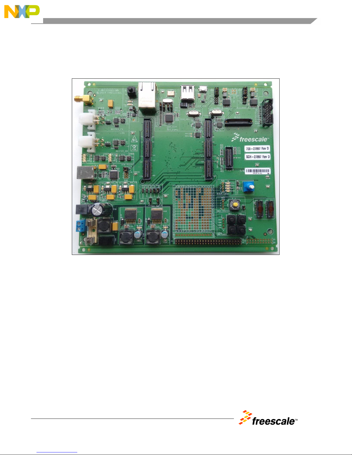
This user guide details the setup and configuration of the Freescale MPC5748G customer Evaluation
Board (hereafter referred to as the EVB). The EVB is intended to provide a mechanism for easy
evaluation of the MPC5748G family of microcontrollers, and to facilitate hardware and software
development. Various daughtercards are available which connect to the EVB via two high density
connectors. Please consult your Freescale representative for more details on daughtercard pricing and
availability.
The EVB is intended for bench / laboratory use and has been designed using normal temperature
specified components (+70°C).
This product contains components that may be damaged by electrostatic discharge. Observe precautions
for handling electrostatic sensitive devices when using this EVB and associated microcontroller.
The user manual is intended to be read alongside the respective MCU documentation available at
www.freescale.com and includes:
Reference Manuals
Product Data Sheets
Application notes
Chip Errata
1.1.
Peripheral Daughtercards
The EVB has connectors for various peripheral daughtercards (for example MLB) that provide
additional peripheral functionality. These are not supplied with the EVB and must be sourced separately.
Please contact your Freescale representative for pricing and availability.
2. EVB Features
The EVB provides the following key features:
Single 10-14 V DC external power supply input with on-board regulators to provide all of the
necessary EVB and MCU voltages. Power may be supplied to the EVB via a 2.1 mm barrel style
power jack or a 2-way screw type connector. 12 V operation allows in-car use if desired.
Master power switch and regulator status LED’s.
USB Serial interface
2 x High Speed CAN transceiver routed to 3-way headers
2 x LIN interfaces routed to standard Molex headers
Main clock supplied from on board crystal or SMA connector
User reset switch with reset status LED’s
Ethernet PHY and RJ45 socket configurable as RMII or MII
USB Type A Host interface
USB Type AB (micro USB) OTG interface
MPC5748G EVB User Guide, User Guide, Rev. 0, 08/2015
3 Freescale Semiconductor, Inc.
Page 4

2 x FlexRay interfaces with standard 2-pin connectors
14-pin JTAG and 50 pin Nexus (Trace) connectors
2 x High Density daughter card connectors allowing an MCU specific daughtercard to be fitted1
MLB daughtercard connector
SAI Audio board connectors (2 x 0.1 inch pitch headers and 2 x TWRPI style headers)
SD connector (mounted to the underside of the board) supporting hardware write protect and
card detection
4 user LEDs wired to MCU ports, also available at a user header
4 user pushbutton switches wired to MCU ports, also available at a user header
Hexadecimal encoded switch wired to 4 MCU ports, also available at a user header
Simple potentiometer connected to analogue input channel
NOTE
To alleviate confusion between jumpers and connector headers, all EVB
jumpers are 2 mm pitch whereas headers are 0.1 inch (2.54 mm). This
prevents inadvertently fitting a jumper to a header.
1
There is no MCU fitted to the EVB. A daughtercard must be fitted before the EVB can be used.
MPC5748G EVB User Guide, User Guide, Rev. 0, 08/2015
4 Freescale Semiconductor, Inc.
Page 5
Configuration Overview
3. Configuration Overview
Throughout this document, all of the default jumper and switch settings are clearly marked with “(D)”
and are shown in blue text. This allows a more rapid return to the default state of the EVB if required.
Note that the default configuration for 3-way jumpers is a header fitted between pins 1 and 2. On the
EVB, 2-way, and 3-way jumpers have been aligned such that pin1 is either to the top or to the left of the
jumper. On 2-way jumpers, the source of the signal is connected to pin1.
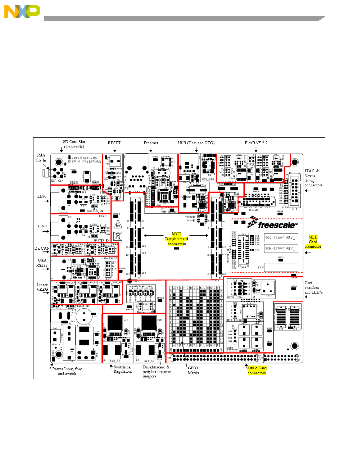
The EVB has been designed with ease of use in mind and has been segmented into functional blocks as
shown below. Detailed silkscreen legend has been used throughout the board to identify all switches,
jumpers and user connectors.
MPC5748G EVB User Guide, User Guide, Rev. 0, 08/2015
Freescale Semiconductor, Inc. 5
Figure 1. EVB Functional Blocks
Page 6
4. MCU Daughtercard information
In order to use the EVB, an MCU daughtercard must be fitted as described in the following section.
Before fitting or removing a daughtercard, ensure the EVB is powered OFF
4.1.
Fitting a daughtercard
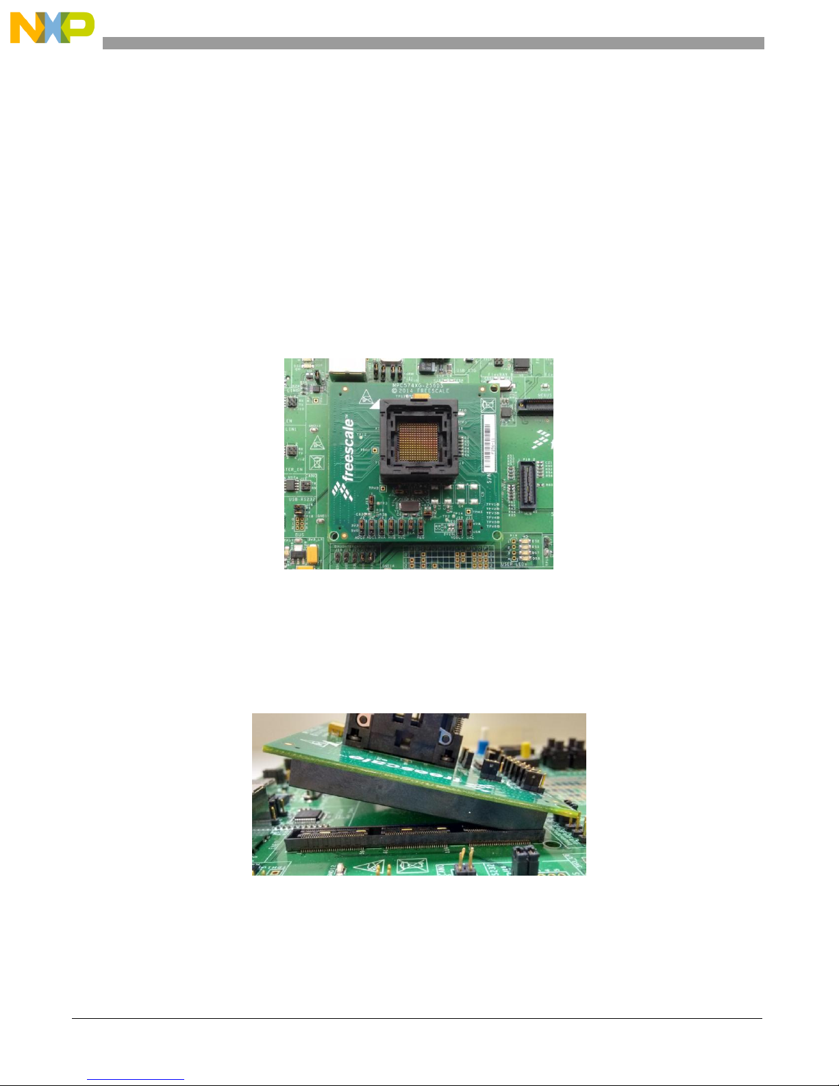
Gently place the daughtercard on the EVB connectors ensuring the correct orientation as shown in the
following figure. The connectors are polarized so the daughtercard will only fit in one orientation (with
the jumpers at the bottom of the daughtercard). Once the connectors have been located correctly, firmly
push down all four corners of the daughter card simultaneously in order to ensure the connectors are
mated. (The following picture also shows the default jumper positions for the 256BGA daughtercard)
Figure 2. Daughtercard Fitted to EVB
4.2.
Removing a daughtercard
In order to prevent damage to the daughtercard connectors, it is important to remove the daughtercard
correctly. Carefully lift either the top or bottom edge of the daughtercard and it should easily lift off as
shown in the following figure (viewed from the left side of the EVB).
Figure 3. Removing a daughtercard
CAUTION
Do not attempt to lift the left or right edge of the daughtercard as this will
result in connector damage.
MPC5748G EVB User Guide, User Guide, Rev. 0, 08/2015
6 Freescale Semiconductor, Inc.
Page 7
Initial Configuration
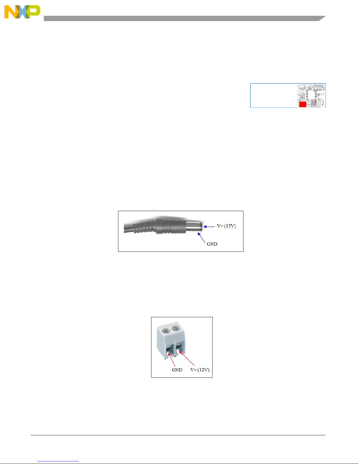
The Power supply
section is located in
the bottom left
corner of the EVB
5. Initial Configuration
This section details the power, reset, clocks, and debug configuration which is the minimum
configuration needed in order to power ON the EVB.
5.1.
Power Supply Configuration
The EVB requires an external power supply voltage of between 10 V-14 V DC (nominal 12 V),
minimum 2 A. This allows the EVB to be used in a vehicle if required. The 12 V input is regulated on
the EVB using two switching and three linear regulators to provide the required voltages of 5.0 V, 3.3 V
(both linear and switcher) and 1.25 V (linear). For flexibility, there are two power supply input
connectors on the EVB as detailed below:
5.1.1.
Power Supply Connectors (P21, P23)
2.1 mm Barrel Connector – P21
This connector should be used to connect the supplied wall-plug mains adapter. Note – if a
replacement or alternative adapter is used, care must be taken to ensure the 2.1 mm plug uses the
correct polarisation as shown below:
Figure 4. 2.1mm Power Connector
2-Way Screw Type Connector – P23
This can be used to connect a bare wire lead to the EVB, typically from a laboratory power supply.
The polarisation of the connectors is clearly marked on the EVB. Care must be taken to ensure
correct connection.
MPC5748G EVB User Guide, User Guide, Rev. 0, 08/2015
Freescale Semiconductor, Inc. 7
Figure 5. 2-Lever Power Connector
Page 8
Jumper
Position
PCB Legend
Description
J23
(INPUT SEL)
1-2 (D)
12V
1.25V Linear regulator is powered from main 12V
2-3
5V
1.25V Linear regulator is powered from 5V switching regulator output
Removed
1.25V Linear regulator is not powered (disabled)
5.1.2.
Power Switch (SW5)
Slide switch SW5 can be used to isolate the power supply input from the EVB voltage regulators if
required.
Moving the slide switch to the right (away from the fuse) will turn the EVB OFF.
Moving the slide switch to the left (towards the fuse) will turn the EVB ON.
5.1.3.
Regulator Power Jumper (J23)
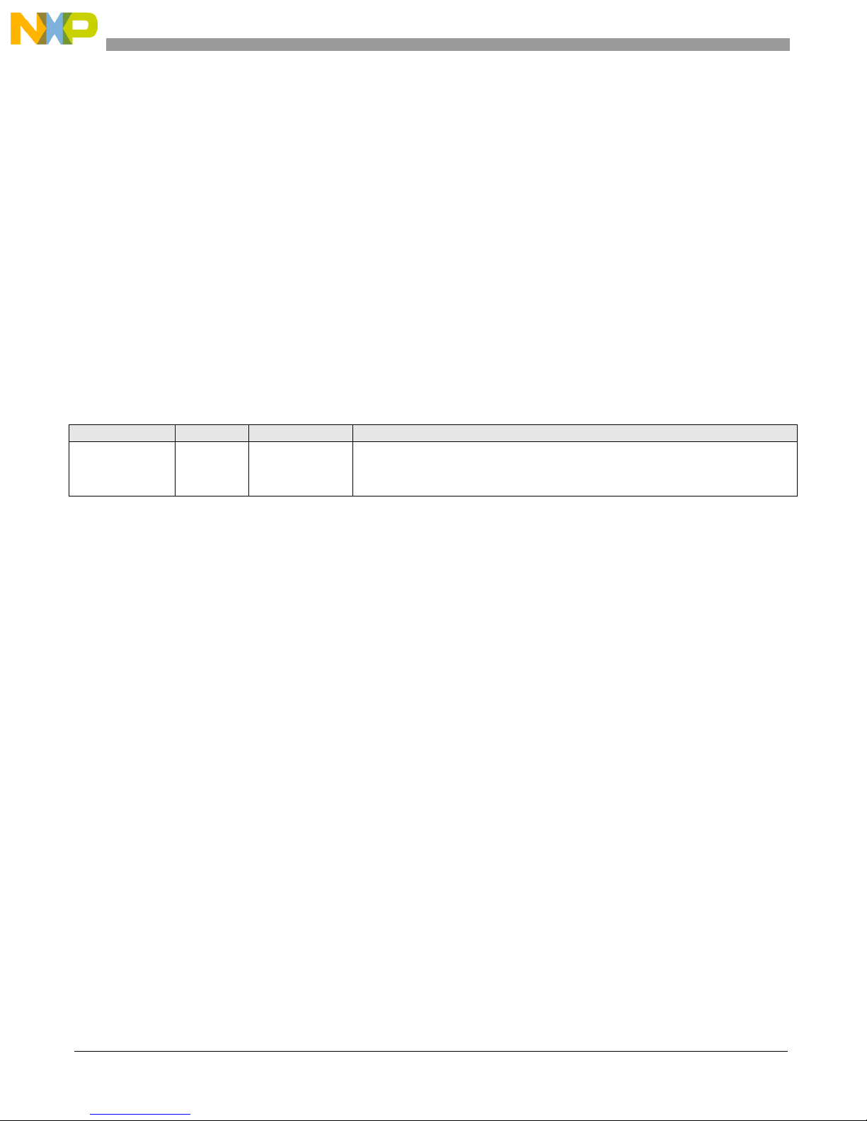
All of the regulators are permanently powered from the main 12 V supply line and active with the
exception of the 1.25 V linear regulator which has a 3-way jumper to allow selection of the input
voltage.
The table below details the jumper configurations for the linear 1.25 V regulator source voltage. By
default, the regulator is powered from the 12 V supply line.
Table 1. 1.25 V Linear Regulator Source Select (J23)
5.1.4.
Power Status LED’s and Fuse
When power is applied to the EVB, five green LED’s adjacent to the voltage regulators show the
presence of the supply voltages as follows:
LED DS4 – Indicates that the 1.25V linear regulator is enabled and working correctly
LED DS5 – Indicates that the 5.0V linear regulator is enabled and working correctly
LED DS6 – Indicates that the 3.3V linear regulator is enabled and working correctly
LED DS9 – Indicates that the 5.0V switching regulator is enabled and working correctly
LED DS10 – Indicates that the 3.3V switching regulator is enabled and working correctly
If no LED’s are illuminated when power is applied to the EVB and the regulators are correctly enabled
using the appropriate jumpers, it is possible that either power switch SW5 is in the “OFF” position or
that the fuse F1 has blown. The fuse is provided to protect the external power supply and for EVB
circuitry reverse-bias protection. If the fuse has blown, check the polarity of your power supply and
replace the fuse with a 20 mm 1.5 A fast blow fuse.
Note that the fuse will not protect against one of the EVB regulators being shorted. If this happens,
damage is likely to occur to the EVB and / or components.
CAUTION
In the event of a short in the regulator output, the regulator and/or the
shorted component may be hot
MPC5748G EVB User Guide, User Guide, Rev. 0, 08/2015
8 Freescale Semiconductor, Inc.
Page 9
Initial Configuration
The MCU Daughtercard
power jumpers are in the
bottom left quarter of the
EVB, above the power
5.1.5.
MCU Power Supply Jumpers
(J18, J19, J20, J21, J22, J23)
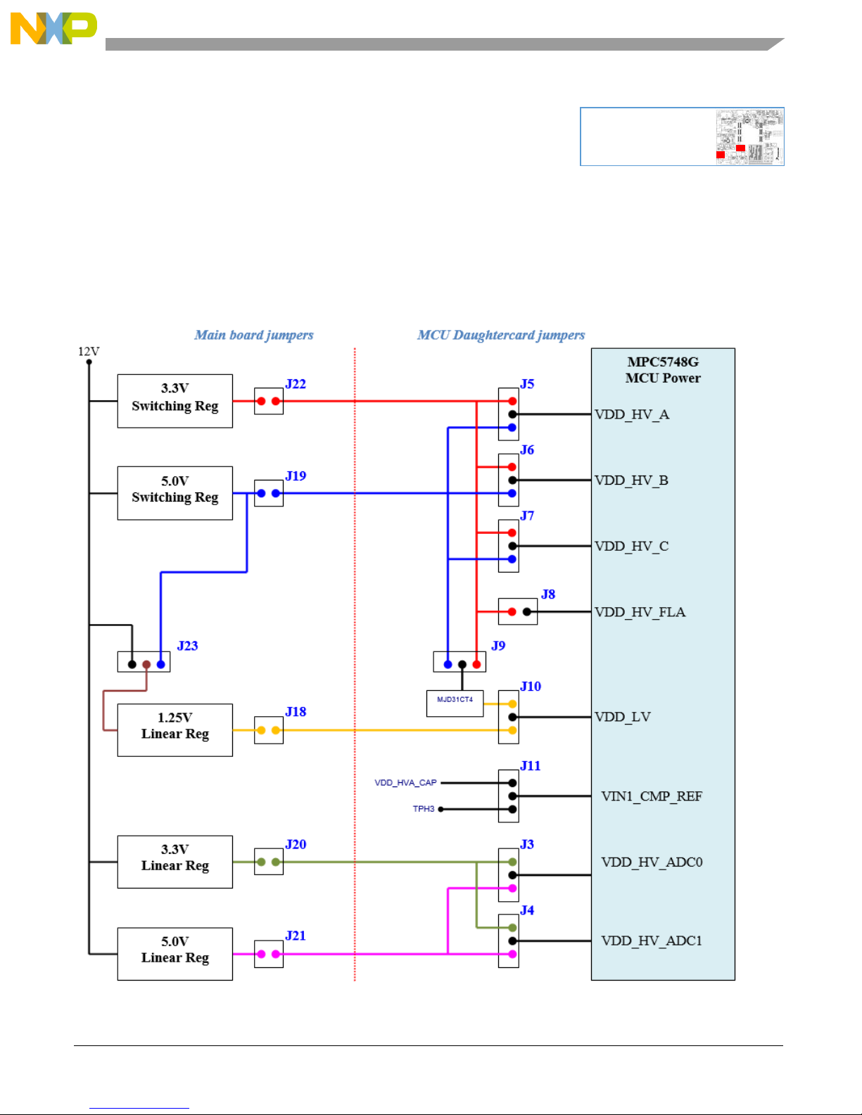
All of the regulated power supplies are routed to the MCU daughtercard via jumpers. This allows each
power supply to be individually isolated and facilitates current measurement at the respective jumper.
Note that only the daughtercard is connected to the power lines after the jumpers so MCU current
measurements are accurate. There are an additional two jumpers that control the voltages used by EVB
peripherals connected to the VDD_HV_A and VDD_HV_B domains as described in section 5.1.7.
MPC5748G EVB User Guide, User Guide, Rev. 0, 08/2015
Freescale Semiconductor, Inc. 9
Figure 6. Power Supply Jumper Schematic
Page 10
Jumper
Position
PCB Legend
Description
J18
1V25L
Fitted (D)
1.25V Linear regulator output is routed to daughter card
Removed
1.25V Linear regulator output is disconnected from daughtercard
J19
5V0S
Fitted (D)
5.0V Switching regulator output is routed to daughter card
Removed
5.0V Switching regulator output is disconnected from daughtercard
J20
3V3L
Fitted (D)
3.3V Linear regulator output is routed to daughter card
Removed
3.3V Linear regulator output is disconnected from daughtercard
J21
5V0L
Fitted (D)
5.0V Linear regulator output is routed to daughter card
Removed
5.0V Linear regulator output is disconnected from daughtercard
J22
3V3S
Fitted (D)
3.3V Switching regulator output is routed to daughter card
Removed
3.3V Switching regulator output is disconnected from daughtercard
J23
INPUT SEL
(Above Power
Jack)
1-2 (D)
12V
1.25v Linear regulator is powered by main 12V input
2-3
5V
1.25v Linear regulator is powered by output from 5.0V switching reg
Removed
1.25v Linear regulator is not powered (disabled)
Jumper
Position
PCB Legend
Description
J3
ADC0
1-2 (D)
3V3
MCU ADC0 pin is connected to 3.3V (Linear)
2-3
5V0
MCU ADC0 pin is connected to 5.0V (Linear)
Removed
MCU ADC0 pin is not connected to power
J4
ADC1
1-2 (D)
3V3
MCU ADC1 pin is connected to 3.3V (Linear)
2-3
5V0
MCU ADC1 pin is connected to 5.0V (Linear)
Removed
MCU ADC1 pin is not connected to power
J5
HVA
1-2 (D)
3V3
MCU VDD_HV_A domain is connected to 3.3V (Switching Regulator)
2-3
5V0
MCU VDD_HV_A domain is connected to 5.0V (Switching Regulator)
Removed
MCU VDD_HV_A domain is not connected to power
J6
HVB
1-2 (D)
3V3
MCU VDD_HV_B domain is connected to 3.3V (Switching Regulator)
2-3
5V0
MCU VDD_HV_B domain is connected to 5.0V (Switching Regulator)
Removed
MCU VDD_HV_B domain is not connected to power
J7
HVC
1-2 (D)
3V3
MCU VDD_HV_C domain is connected to 3.3V (Switching Regulator)
2-3
5V0
MCU VDD_HV_C domain is connected to 5.0V (Switching Regulator)
Removed
MCU VDD_HV_C domain is not connected to power
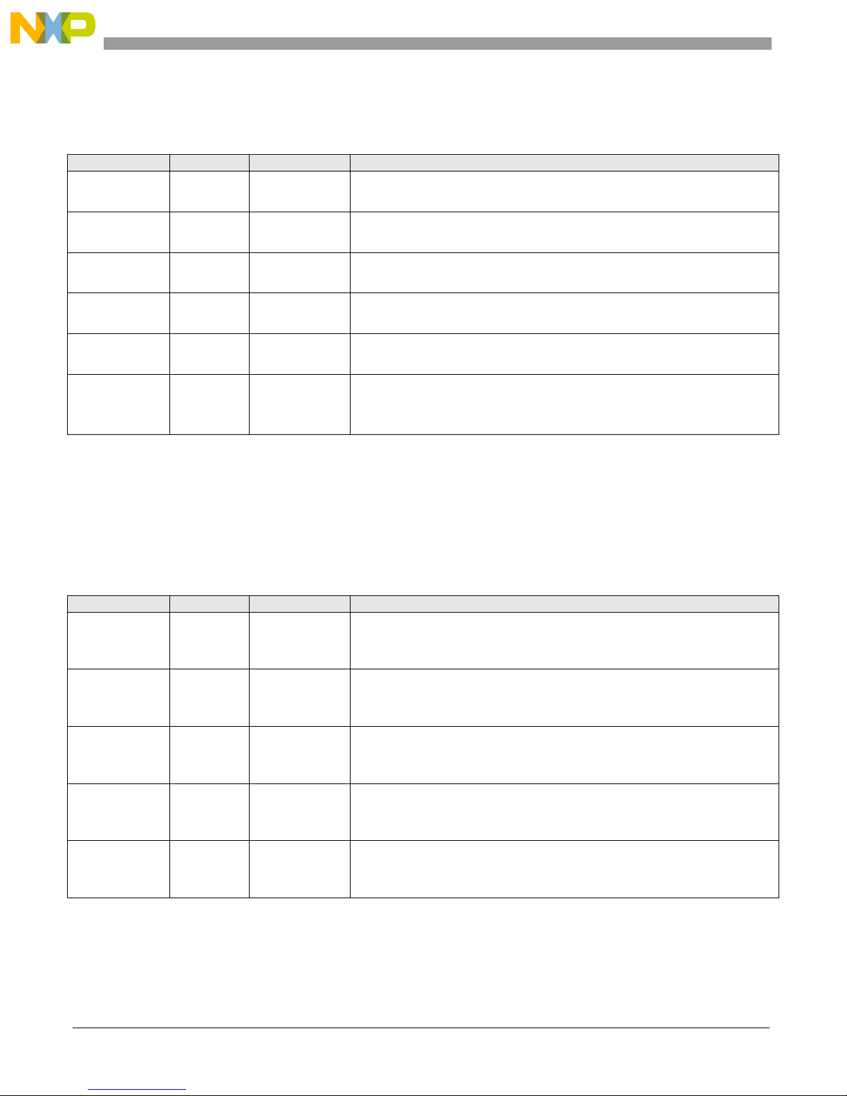
The power supply jumper description table is shown in the following table:
Table 2. Daughter Card Power Supply Jumpers (on main board)
5.1.6.
The following power control jumpers are located on the MCU daughtercard. Note that not all of the
jumpers will be on each daughtercard variant.
Daughtercard Power Jumpers (J3 to J11)
Table 3. MCU Power Supply Jumpers (on daughtercard)
MPC5748G EVB User Guide, User Guide, Rev. 0, 08/2015
10 Freescale Semiconductor, Inc.
Page 11
Initial Configuration
Jumper
Position
PCB Legend
Description
J8 2
FLA
Fitted (D)
MCU VDD_HV_FLA pin is connected to 3.3v (Switching Regulator)
Removed
MCU VDD_HV_C domain is connected to 5.0V (Switching Regulator)
J9
REG
1-2 (D)
3V3
MCU ballast transistor collector is connected to 3.3V (Switching)
2-3
5V0
MCU ballast transistor collector is connected to 5.0V(Switching)
Removed
MCU ballast transistor collector is not connected to power
J10
VDDLV
1-2 (D)
REG
MCU VDD_LV domain is powered from ballast transistor
2-3
1V25L
MCU VDD_LV domain is powered from 1.25V Linear regulator
Removed
MCU VDD_LV domain is not powered
J11
DAC
1-2 (D)
HVA
MCU VIN1_CMP_REF is powered from VDD_HV_A
2-3
USR
MCU VIN1_CMP_REF is powered from user testpoint (TPH3)
Removed
MCU VIN1_CMP_REF is not powered
Jumper
Position
PCB Legend
Description
J24
HVA
1-2 (D)
3V3
EVB peripherals in HVA domain are set to use I/O voltage of 3.3V
2-3
5V0
EVB peripherals in HVA domain are set to use I/O voltage of 5.0V
Removed
Invalid Configuration, avoid!
J25
HVB
1-2 (D)
3V3
EVB peripherals in HVB domain are set to use I/O voltage of 3.3V
2-3
5V0
EVB peripherals in HVB domain are set to use I/O voltage of 5.0V
Removed
Invalid Configuration, avoid!
The peripheral power
jumpers are in the bottom
left quarter of the EVB,
above the power area
5.1.7.
Peripheral Power Supply Jumpers (J24, J25)
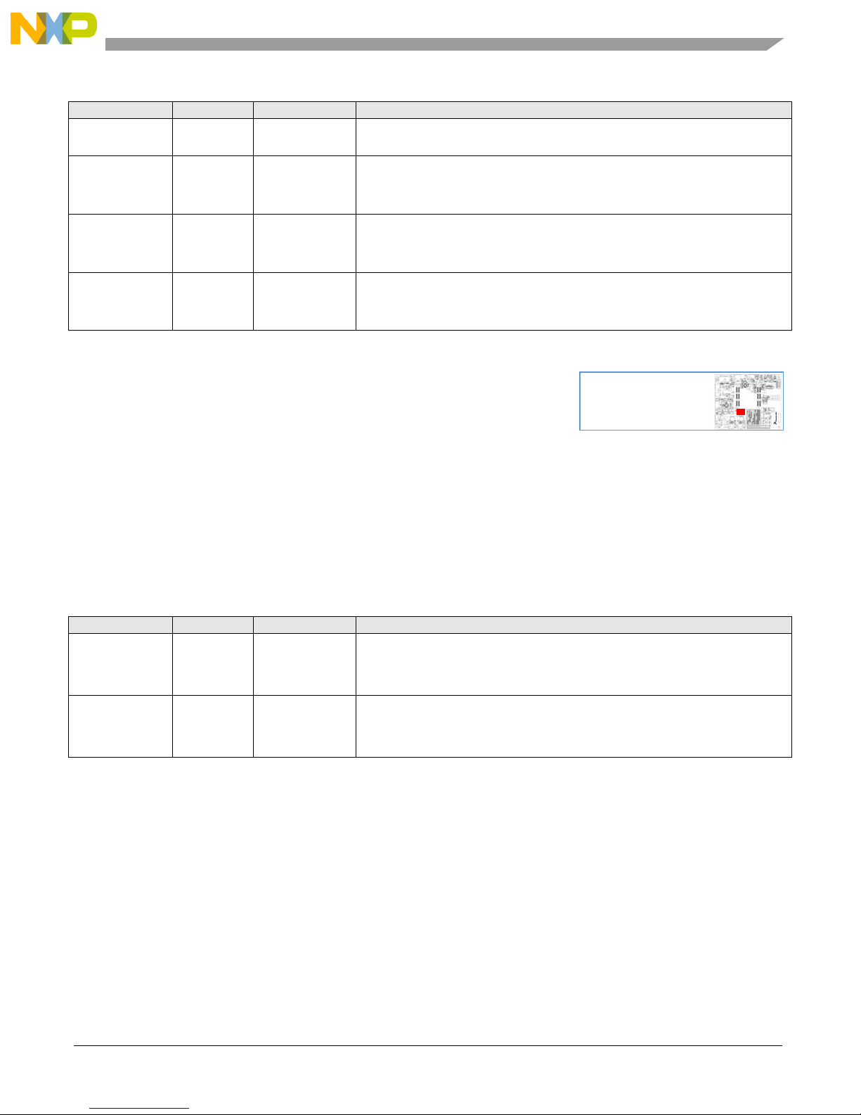
There are two additional power supply jumpers controlling the I/O voltage for the peripherals on the
EVB in the HVA and HVB voltage domains.
The settings on these jumpers must match the VDD_HV_A and VDD_HV_B jumper voltage setting on
the MCU daughtercard.
The default configuration matches the MCU daughtercard default configuration with both jumpers set to
3.3V.
Table 4. Peripheral Power Control (J24, J25)
5.1.8.
EVB Voltage Regulators
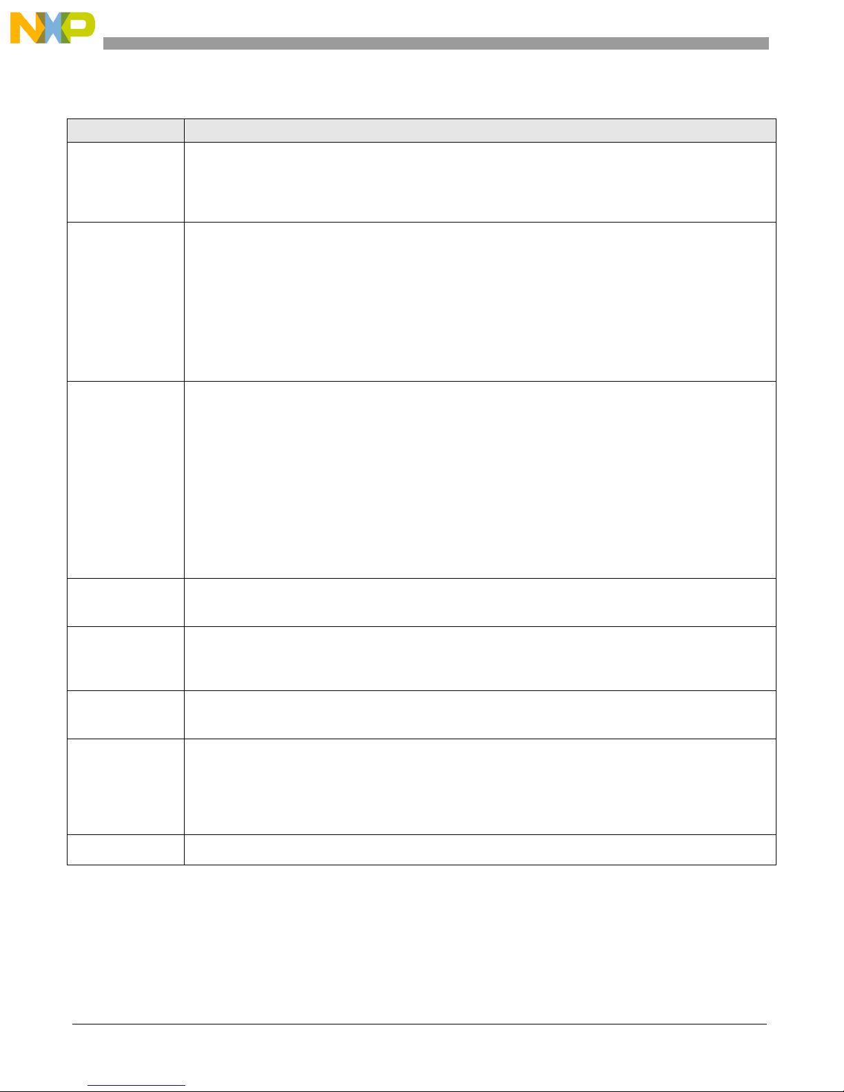
The following table shows the usage of each EVB voltage regulator. This provides a useful cross
reference point should any regulator be disabled. In addition, the distribution of the peripheral voltages
HVA (J24) and HVB (J25) are shown.
2
Note that jumper J8 (FLA) jumper must only be fitted when VDD_HV_A (J5) is connected to 3.3V.
MPC5748G EVB User Guide, User Guide, Rev. 0, 08/2015
Freescale Semiconductor, Inc. 11
Page 12
Regulator
Used On
12V
(Unregulated)
P12V
All voltage regulators (switching and Linear, jumper selectable on 1.25V linear)
1.25V linear regulator LED supply via FET
MCU Daughtercard connector
MLB Daughtercard connector
FlexRay transceiver VBAT pin
5.0V
Switcher
5V0_SR
Daughtercard connector (post daughtercard power jumper)
Daughtercard connector (direct feed via zero ohm link)
Peripheral power control jumpers (position 2-3)
CAN transceivers VCC (main power)
USB RS232 (FTDI) transceiver (main power and protection diode)
USB Host / OTG transceiver power (VBAT) pin
FlexRay Transceiver power pins (VCC / VBUF)
SAI Audio connector
Input to 1.25V linear regulator (in alternate jumper configuration)
3.3V
Switcher
3V3_SR
Daughtercard connector (post daughtercard power jumper)
Daughtercard connector (direct feed via zero ohm link)
Peripheral power control jumpers (position 1-2)
Reset LED’s (user and target)
USB HOST / OTG transceiver I/O voltage (USB operation is fixed at 3.3V)3
Ethernet Transceiver supply and I/O (Ethernet operation is fixed at 3.3V) 3
SAI Audio connector
MLB Daughtercard connector
SD Card power supply / pullup resistors (SD Card operation is fixed at 3.3V)3
User LED’s supply voltage
Hex encoder switch supply voltage
User pushbutton switches supply voltage
5.0V
Linear
5V0_LR
Daughtercard connector (post daughtercard power jumper)
Daughtercard connector (direct feed via zero ohm link)
3.3V
Linear
3V3_LR
Daughtercard connector (post daughtercard power jumper)
Daughtercard connector (direct feed via zero ohm link)
MLB Daughtercard connector
ADC Input Pot (user variable resistor)
1.25V
Linear
1V25_LR
Daughtercard connector (post daughtercard power jumper)
Daughtercard connector (direct feed via zero ohm link)
J24 PER_HVA
Reset control circuitry (including reset pullup)
JTAG Pullup resistors & reference voltage
CAN Transceiver I/O Voltage select
LIN Transceiver Enable (and I/O voltage select)
USB RS232 (FTDI) transceiver I/O voltage select
FlexRay Transceiver I/O Voltage select (and pullups)
J25 PER_HVB
Nexus Connector reference voltage and Pullups
Table 5. Power Supply Distribution
3
These voltages are fixed due to device specifications and cannot be changed.
12 Freescale Semiconductor, Inc.
MPC5748G EVB User Guide, User Guide, Rev. 0, 08/2015
Page 13
Initial Configuration
Jumper
Position
PCB Legend
Description
J9 (EN)
Fitted (D)
Reset from reset switch and debug connectors is active
Removed
Reset from reset switch and debug connectors is inactive
The reset circuitry and
switch are located in the
top left quarter of the
EVB next to theRJ45
Note that the JTAG pins are in domain VDD_HV_A whereas the Nexus pins are VDD_HV_B.
Normally this would mean that for trace, the HVA and HVB domains should be at the same voltage
however some development tools can automatically adapt to the voltages on the trace signals. Please
consult your tools vendor for further details.
5.2.
Reset Control (J9, SW1)
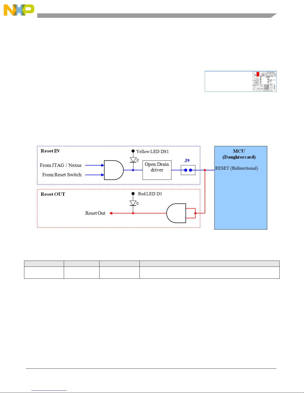
The MCU has a single bi-directional open drain Reset pin. Rather than connect multiple devices to the
reset pin directly, a reset-in and reset-out buffering scheme has been implemented on the EVB as shown
in Figure 7 below. The reset “in” from the reset switch (SW1) and the debug connectors are logically
OR’d together using an AND gate and then connected to the buffer to provide an open-drain output.
The “reset-out” circuitry provides a buffered reset signal that can be used to drive any circuitry requiring
a reset control from the MCU.
Jumper J9 is used to disconnect the reset signal from the external reset sources if required.
Note that removing jumper J9 will mean that an external reset source will not reset the MCU. This will
impact most debuggers which will typically issue a reset before establishing a debug connection.
5.2.1.
Reset LEDs
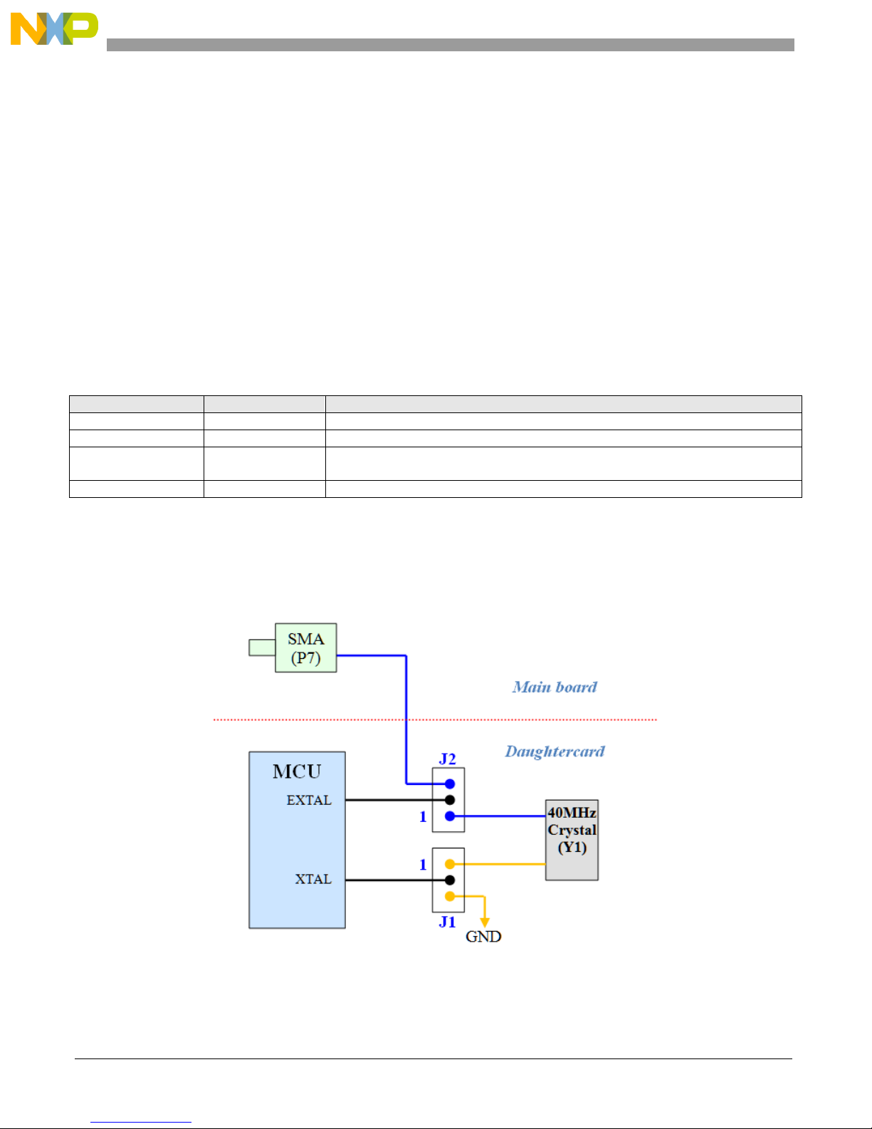
As can be seen in Figure 7 above, there are two reset LED’s that can be used to identify the source /
cause of a reset:
MPC5748G EVB User Guide, User Guide, Rev. 0, 08/2015
Freescale Semiconductor, Inc. 13
Figure 7. EVB Reset Control
Table 6. Reset Control (J9)
Page 14
LED DS1 (Yellow)
LED D1 (Red)
Description
OFF
OFF
No Reset being issued from MCU or external logic
OFF
ON
MCU has issued a reset
ON
OFF
External reset issued from switch or debug BUT not being issued to MCU
(check J9 is fitted on the EVB)
ON
ON
External reset issued from reset switch or debug and has been issued to MCU.
RED LED D1 (titled “MCU”) will illuminate if:
The MCU issues a reset (in this condition ONLY this LED will be illuminated and LED DS1
will be off)
There is a target reset (ie from the reset switch or from the debugger in which case LED DS1
will be ON)
YELLOW LED DS1 (titled “USR”) will illuminate when an external hardware device issues a reset to
the MCU:
The reset switch is pressed
There is a reset being driven from one of the debug connectors
Table 7. Reset LED Decoding
MCU Clock Configuration
5.3.
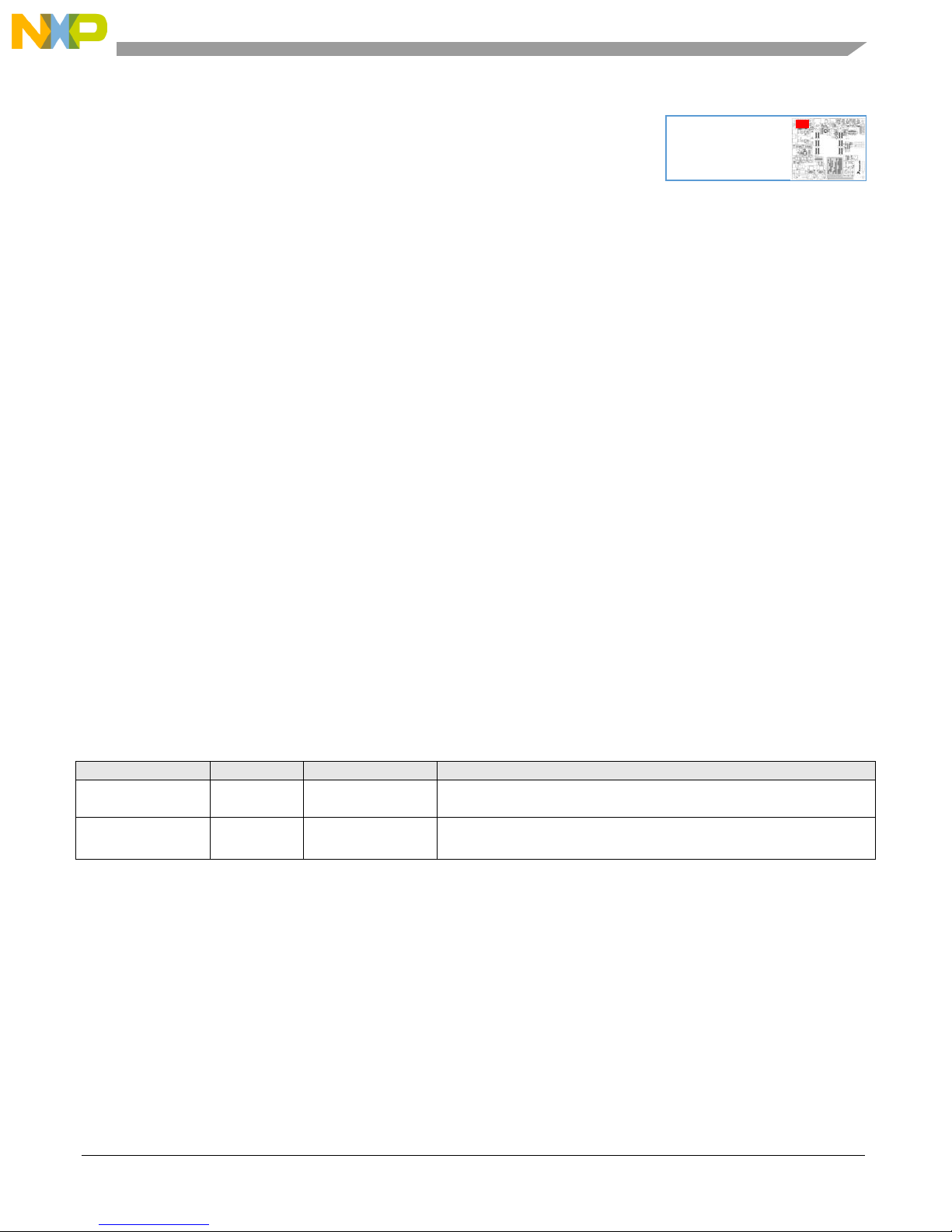
There are 2 clock configuration jumpers on the daughtercard and an external clock input connector on
the main board to allow an externally generated clock to be supplied if desired. See Figure 8 below.
Figure 8. EVB Clock Selection
MPC5748G EVB User Guide, User Guide, Rev. 0, 08/2015
14 Freescale Semiconductor, Inc.
Page 15
Initial Configuration
Jumper
Position
PCB Legend
Description
J1 (XTAL)
1-2 (D)
Y1
MCU XTAL signal is routed to crystal Y1
2-3
GND
MCU XTAL signal is Grounded (for ext clock mode)4
J2 (EXTAL)
1-2 (D)
Y1
MCU EXTAL signal is routed to crystal Y1
2-3
EXT
MCU EXTAL signal is routed from EVB SMA P7
The external SMA
clock connector is
located in the top left
corner of the EVB
5.3.1.
External Clock Input (P7)
The external clock input on the EVB is applied via SMA connector P7. When driving an external clock
into the SMA connector, the jumpers on the daughtercard must be reconfigured to route the external
clock to the MCU.
Note that the following conditions must be met when supplying an external clock:
The clock frequency must be between 8MHz and 40MHz
The amplitude of the clock input should not exceed the voltage being driven into the
VDD_HV_A pins. This is selectable between 3.3V and 5.0V on the daughtercard.
5.3.2.
MCU Clock Configuration (J1, J2 on Daughtercard)
There are two external clock crystals on the MPC5748G daughtercards:
40MHz fast external crystal for clocking the main system clock
32KHz slow external crystal for accurate time of day keeping
The 40MHz crystal is connected to the MCU XTAL and EXTAL pins via 3-way jumper headers as
shown in the diagram above. These jumpers allow an external clock to be routed from the SMA
connector (P7) on the main board if desired. The default configuration is with both daughtercard
jumpers (J1 and J2) set to position 1-2 which routes the external 40MHz crystal to the MCU pins. If you
wish to supply a clock via the SMA connector on the main EVB, move the daughtercard jumpers J1 and
J2 to position 2-3.
The 32 KHz external crystal is permanently connected to the MCU EXTAL32 and XTAL32 pins and
has no configuration options.
Table 8. EXTAL Clock Source Selection (J1, J2 Daughtercard)
4
Note that the XTAL pin is left open by default with J1 in position 2-3. Resistor R34 must be populated with a zero
ohm resistor in order to ground the XTAL pin.
MPC5748G EVB User Guide, User Guide, Rev. 0, 08/2015
Freescale Semiconductor, Inc. 15
Page 16
Pin No
Function
Connection
Pin No
Function
Connection
1
TDI
PC0 2 GND
GND
3
TDO
PC1 4 GND
GND
5
TCLK
PH9 6 GND
GND
7
EVTI
PL8 8 N/C
--- 9 RESET
JTAG-RSTx
10
TMS
PH10
11
VREF
PER_HVA
12
GND
GND
13
RDY
---
14
JCOMP
10K Pulldown
Pin No
Function
Connection
Pin No
Function
Connection
1
MSEO_0
PL9 2 VREF
PER_HVB
3
MSEO_1
PL11 4 TCK
PH9 5 GND
GND 6 TMS
PH10
7
MDO0
PL2 8 TDI
PC0
9
MDO1
PL3
10
TDO
PC1
11
GND
GND
12
JCOMP
10K Pulldown
13
MDO2
PL4
14
RDY
---
15
MDO3
PL5
16
EVTI
PL8
17
GND
GND
18
EVTO
PL12
19
MCKO
PL10
20
RESET
DBUG_RST
21
MDO4
PL6
22
RST_OUT
MCU_RST
23
GND
GND
24
GND
GND
25
MDO5
PL7
26
CLKOUT
Test Point
27
MDO6
PL13
28
TD/WT
---
29
GND
GND
30
GND
GND
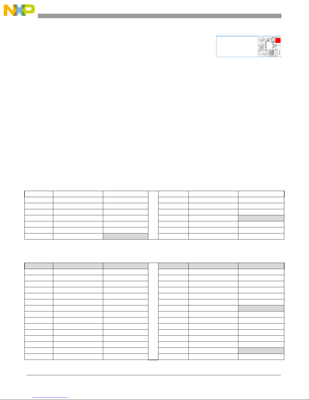
The JTAG and
Nexus debug
connectors are in
the top right corner
5.4.
Debug Connectors (P8, P10)
The EVB provides two debug connectors:
Standard 14 pin JTAG
50 Pin Nexus connector (Samtec ASP-148422-01, Nexus Standard HP50 connector)
There is no user configuration required to use the connectors however the following points should be
noted:
The JTAG connector is routed to the JTAG signals in the default position which are powered
from the MCU VDD_HV_A power domain. The Nexus signals are located in the VDD_HV_B
power domain. If you are using Nexus, you may have to ensure that the VDD_HV_A and
VDD_HV_B domains are at the same voltage. Consult your tools vendor for specific information
The Nexus signals are not bonded out in every MCU package. Before using Nexus, please ensure
the MCU fitted to the EVB (via the daughtercard) supports the Nexus signals.
5.4.1.
Debug Connector Pinouts
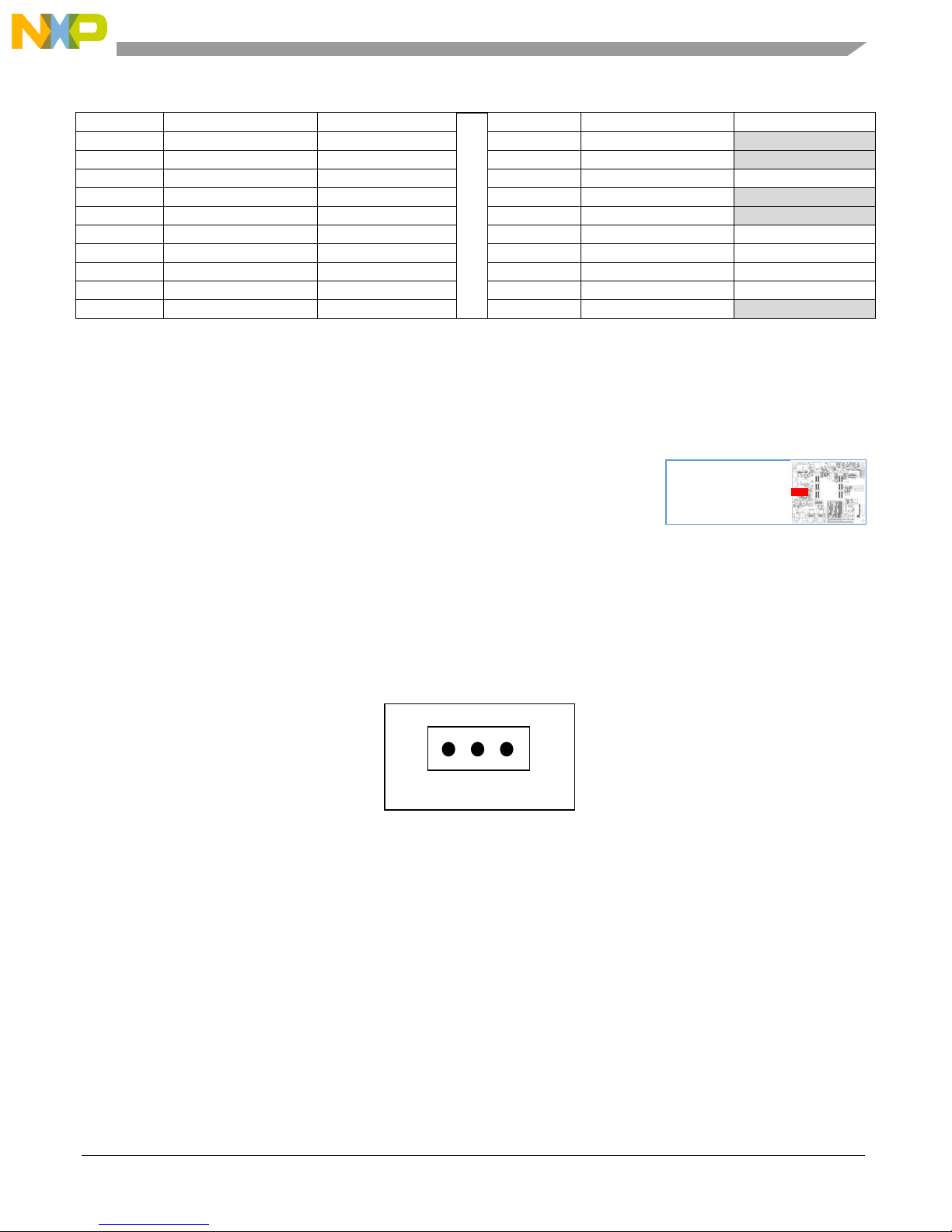
The following tables list the pinouts for each of the debug connectors used on the EVB
Table 9. 14-Pin JTAG Debug Connector Pinout
Table 10. 50-pin Samtec (Nexus) Debug Connector Pinout
MPC5748G EVB User Guide, User Guide, Rev. 0, 08/2015
16 Freescale Semiconductor, Inc.
Page 17
Communications & Memory Interfaces:
Pin No
Function
Connection
Pin No
Function
Connection
31
MDO7
PL14
32
DAI1
---
33
MDO8
PL15
34
DAI2
---
35
GND
GND
36
GND
GND
37
MDO9
PM0
38
ARBREQ
---
39
MDO10
PM1
40
ARBGRT
---
41
GND
GND
42
GND
GND
43
MD011
PM2
44
MDO13
PM8
45
MDO12
PM7
46
MDO14
PM9
47
GND
GND
48
GND
GND
49
MDO15
PM10
50
N/C
---
H
L
GND
1
The CAN Physical
interface circuits are
located on the left
edge of the EVB
6. Communications & Memory Interfaces:
This section details the communication interface and storage peripherals that are implemented on the
EVB.
6.1.
CAN Interfaces (P14, P15, J14, J15)
The EVB incorporates two identical CAN interface circuits connected to MCU CAN0 and CAN1 using
MC33901 transceivers. Both transceivers are configured for high speed operation by pulling pin 8 to
GND via a 4.7K Ohm resistor. There are test points to allow the Select pin to be driven high if desired.
The MC33901 is pin compatible with other CAN transceivers supporting full CAN FD data rates.
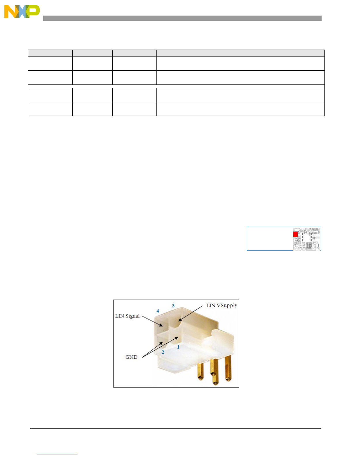
For flexibility, the CAN transceiver I/O is connected to a standard 0.1” connector (P14 for CAN1 / P15
for CAN0) rather than using non standard DB9 connectors. The pinout of these headers is shown below
and is also detailed on the PCB silkscreen
Figure 9. CAN Physical Interface Connectors
The CAN0 and CAN1 MCU TX/RX signals are jumpered as shown in the table below to allow the
transceivers to be isolated from the respective MCU pin if desired. The default configuration is with all
jumper headers fitted routing the TX and RX signals to the MCU.
MPC5748G EVB User Guide, User Guide, Rev. 0, 08/2015
Freescale Semiconductor, Inc. 17
Page 18
Jumper
Position
PCB Legend
Description
J15 (CAN0)
Posn 1-2
FITTED (D)
TX
MCU CAN0_TX signal (PB0) is routed to CAN interface
Removed
MCU CAN0_TX signal (PB0) is not routed to CAN interface
J15 (CAN0)
Posn 3-4
FITTED (D)
RX
MCU CAN0_RX signal (PB1) is routed to CAN interface
Removed
MCU CAN0_RX signal (PB1) is not routed to CAN interface
J14 (CAN1)
Posn 1-2
FITTED (D)
TX
MCU CAN1_TX signal (PC10) is routed to CAN interface
Removed
MCU CAN1_TX signal (PC10) is not routed to CAN interface
J14 (CAN1)
Posn 3-4
FITTED (D)
RX
MCU CAN1_RX signal (PC11) is routed to CAN interface
Removed
MCU CAN1_RX signal (PC11) is not routed to CAN interface
The LIN Physical
interface circuits are
located on the left
edge of the EVB
Table 11. CAN Control Jumpers (J51, J53)
NOTE
Care should be taken when fitting the jumper headers to the 2x2 jumper
blocks J14 and J15 as they can easily be fitted in the incorrect orientation.
Jumper headers should be fitted horizontally.
The CAN TX / RX MCU pins are powered from the VDD_HV_A domain, which is configured between
3.3V and 5.0V on the daughtercard using jumper J5. The CAN transceivers I/O voltage is connected to
the PER_HVA net configured with jumper J24 on the main EVB. Care must be taken to ensure that the
MCU VDD_HV_A and PER_HVA supplies are the same when using the CAN transceiver.
6.2.
LIN Interfaces (P9, P11, J10, J12)
The EVB incorporates two identical LIN transceiver circuits connected to MCU LIN0 and LIN1 using a
Freescale MC33662LEF transceiver supporting both master and slave mode (jumper selectable)
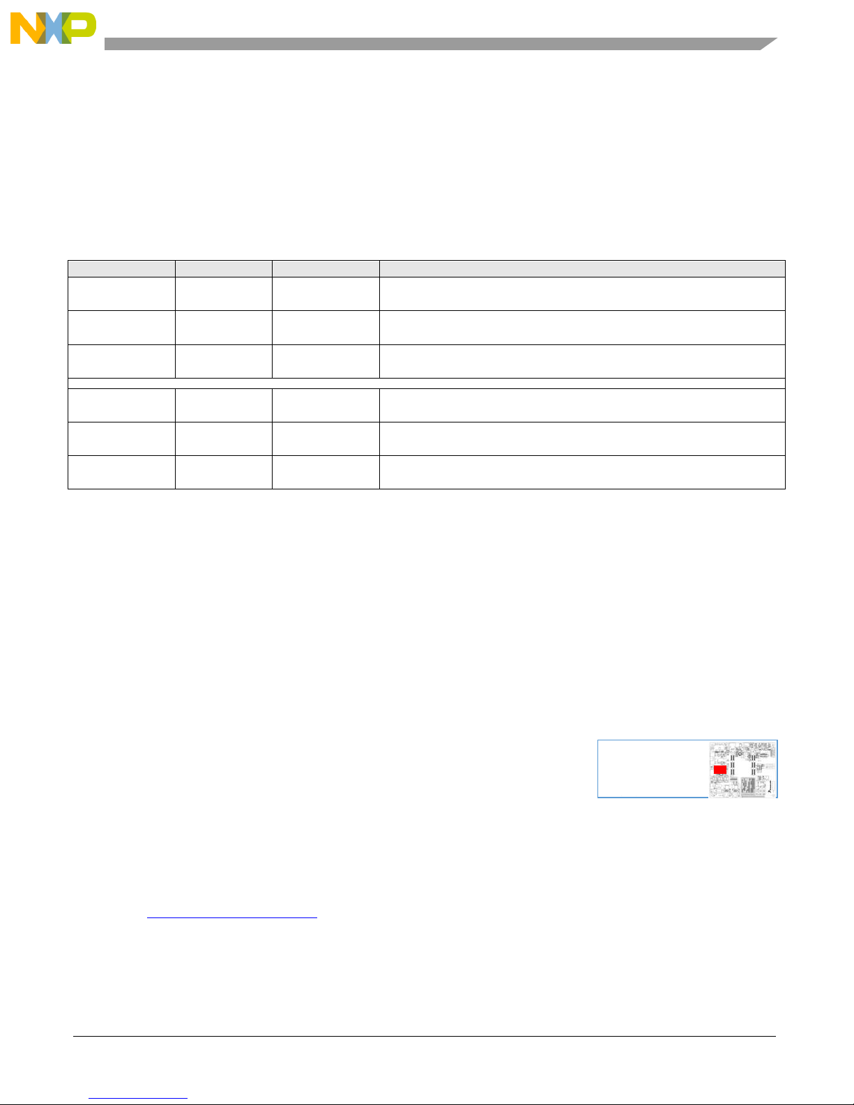
The output from the LIN transceiver is connected to a standard 4-pin Molex connector as used on most
other Freescale EVB’s supporting LIN as shown in the following figure:
Figure 10. LIN Molex Physical Interface Connector
MPC5748G EVB User Guide, User Guide, Rev. 0, 08/2015
18 Freescale Semiconductor, Inc.
Page 19
Communications & Memory Interfaces:
Jumper
Position
PCB Legend
Description
J10 (LIN0)
Posn 1-2
FITTED (D)
RX
MCU LIN0_RX signal (PB3) is routed to LIN0 interface
Removed
MCU LIN0_RX signal (PB3) is not routed to LIN0 interface
J10 (LIN0)
Posn 3-4
FITTED (D)
TX
MCU LIN0_TX signal (PB2) is routed to LIN0 interface
Removed
MCU LIN0_TX signal (PB2) is not routed to LIN0 interface
J11
(Master_EN)
FITTED (D)
LIN0 is configured in Master Mode
Removed
LIN0 is configured in Slave Mode
J12 (LIN1)
Posn 1-2
FITTED (D)
RX
MCU LIN1_TX signal (PC7) is routed to LIN1 interface
Removed
MCU LIN1_TX signal (PC7) is not routed to LIN1 interface
J12 (LIN1)
Posn 3-4
FITTED (D)
TX
MCU LIN1_RX signal (PC6) is routed to LIN interface
Removed
MCU LIN1_RX signal (PC6) is not routed to LIN interface
J13
(Master_EN)
FITTED (D)
LIN1 is configured in Master Mode
Removed
LIN1 is configured in Slave Mode
The USB RS232
interface is on the
left hand edge of the
board (USB Type B
The LIN0 and LIN1 MCU TX/RX signals are jumpered as shown in the following to allow the
transceivers to be isolated from the respective MCU pin if desired. The default configuration is with all
jumper headers fitted routing the TX and RX signals to the MCU.
Each transceiver also has a master mode enable jumper which is fitted by default to configure the
transceiver for Master mode. To configure the transceiver for slave mode, remove the respective
“Master_EN” jumper.
Table 12. LIN Control Jumpers (J10, J11, J12, J13)
NOTE
Care should be taken when fitting the jumper headers to the 2x2 jumper
blocks J10 and J12 as they can easily be fitted in the incorrect orientation.
Jumper headers should be fitted horizontally
The LIN TX / RX MCU pins are powered from the VDD_HV_A domain, which is configured between
3.3V and 5.0V on the daughtercard using jumper J5. The LIN transceivers enable pin is connected to the
PER_HVA net configured with jumper J24 on the main EVB. Care must be taken to ensure that the
MCU VDD_HV_A and PER_HVA supplies are the same when using the LIN transceiver.
Note that in order for the LIN transceiver to function, external power must be supplied via pin 3 of the
molex connector as detailed in Figure 10.
6.3.
USB RS232 Serial Interface (P17, J16)
The EVB incorporates a USB RS232 serial interface providing RS232 connectivity via a direct USB
connection between the PC and the EVB. The circuit contains an FTDI FT2232D USB to Serial
interface which should automatically install the drivers for two additional COM ports on your PC. Note
that only one of these is used so you will need to try both (usually the higher numbered COM port is the
active one). For more information on the USB drivers and general fault finding, consult the FTDI
website at http://www.ftdichip.com/
The MCU LIN2 signals are routed to the FTDI transceiver via a 2-way jumper header (J16) allowing the
transceiver to be isolated from the MCU pin if desired. The default configuration is with the jumper
MPC5748G EVB User Guide, User Guide, Rev. 0, 08/2015
Freescale Semiconductor, Inc. 19
Page 20
Jumper
Position
PCB Legend
Description
J16
Posn 1-2
FITTED (D)
RX
MCU LIN2_RX signal (PC9) is routed to the FTDI interface
Removed
MCU LIN2_RX signal (PC9) is not routed to the FTDI interface
J16
Posn 3-4
FITTED (D)
TX
MCU LIN2_TX signal (PC8) is routed to the FTDI interface
Removed
MCU LIN2_TX signal (PC8) is not routed to the FTDI interface
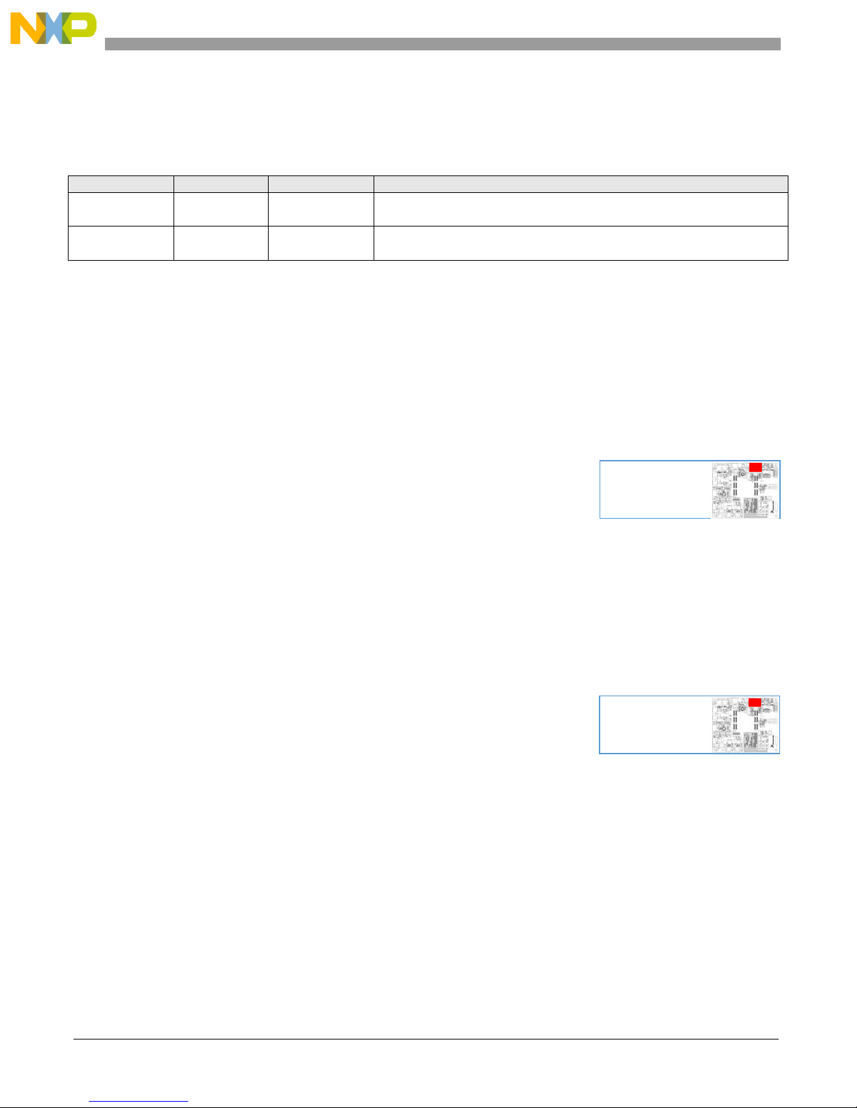
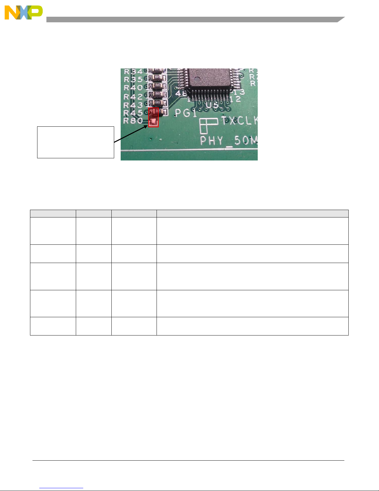
The USB interfaces
are on the top right
quarter on the board
on the top edge
The USB interfaces
are on the top right
quarter on the board
on the top edge
header fitted, routing the TX and RX signals from the MCU to the FTDI transceiver. No other
configuration is required.
Table 13. USB RS232 Control Jumpers
NOTE
Care should be taken when fitting the jumper headers to the 2x2 jumper
block J16 as they can easily be fitted in the incorrect orientation. Jumper
headers should be fitted horizontally.
The MCU LIN2 (SCI) pins are powered from the VDD_HV_A domain, which is configured between
3.3V and 5.0V on the daughtercard using jumper J5. The FTDI transceiver I/O voltage pin is connected
to the PER_HVA net configured with jumper J24 on the main EVB. Care must be taken to ensure that
the MCU VDD_HV_A and PER_HVA supplies are the same when using the FTDI transceiver.
6.4.
USB HOST / OTG Interfaces
The EVB includes Type A (Host) and Type AB (OTG) USB interfaces, routed to standard and micro
USB sockets respectively. Each USB circuit contains a USB83340 transceiver with a shared USB power
switch. There is no user configuration required on either of the USB circuits.
The USB transceivers have a 3.3V (only) interface. All of the USB0 (connected to the OTG transceiver)
and USB1 (connected to the HOST transceiver) signals are in the VDD_HV_A domain and must be
configured as 3.3V via daughtercard jumper J5. If VDD_HV_A is set to 5V, the USB0 and USB1 MCU
signals should be left tri-stated to prevent damage to the USB transceivers.
6.5.
Ethernet (P6, J5, J6, J7, J8, R45, R80)
The MPC5748G supports both MII and RMII Ethernet interfaces. The EVB incorporates a DP83848c
transceiver supporting both MII and RMII modes. The transceiver is connected to a pulse J1011F21PNL
RJ45 connector which includes a built-in isolation transformer.
The default configuration, with all 2-way jumpers fitted and all 3-way jumpers in position 1-2,
configures the transceiver for MII mode with the reset signal to the PHY being driven from the MCU
Reset out (eg any reset causing the MCU Reset line to assert will reset the PHY)
In order to configure the EVB for RMII mode, jumpers J5, J6 and J7 need to be changed as described in
Table 14 below. In addition, a surface mount 0Ω resistor needs to be de-soldered and moved as shown in
the figure below. This option is fitted as a resistor instead of a jumper to maintain signal integrity on the
Ethernet clock signal.
MPC5748G EVB User Guide, User Guide, Rev. 0, 08/2015
20 Freescale Semiconductor, Inc.
Page 21
Communications & Memory Interfaces:
Jumper
Position
PCB Legend
Description
J5
1-2 (D)
MII
Ethernet PHY is configured in MII mode
2-3 R Ethernet PHY is configured in RMII mode
Removed
Invalid Configuration, avoid!
J6
(X1)
1-2 (D)
Ethernet PHY X2 clock is connected to 25MHz xtal
2-3 Ethernet PHY X2 clock is not connected to 25MHz xtal5, 6
J7
(X2)
1-2 (D)
Ethernet PHY X1 clock is connected to 25MHz xtal
2-3 Ethernet PHY X1 clock is driven from 50MHz xtal
Removed
Ethernet PHY X1 clock is disconnected (invalid configuration, avoid)
J8
(RST)
1-2 (D)
NORM
The Ethernet PHY will be reset along with MCU reset
2-3
PI11
The Ethernet PHY reset is controlled via MCU pin PI11 (Pulled high)
Removed
Invalid Configuration, avoid!
R45 (R80)
Fitted R45
MII Mode – Clock is supplied from PHY to MCU
R45 to R80
RMII Mode – Clock is supplied from external 50MHz oscillator to MCU
For RMII mode
remove R45 and re-fit
in this position
For MII mode (default) R45 should have a jumper populated as shown. For RMII mode, remove R45
and fit it between R45 and R80
Figure 11. MII / RMII Clock Selection Resistor
To change the reset routing so that the Ethernet PHY can be reset via MCU pin PI11 (rather than being
tied to the MCU reset), jumper J8 should be moved to position 2-3
Table 14. Ethernet Control jumpers (J5, J6, J7, J8, R45, R80)
The MCU Ethernet signals are all in the VDD_HV_B domain. The Ethernet PHY will ONLY function
with 3.3V I/O so VDD_HV_B must be set to 3.3V on the MCU daughtercard before the Ethernet is
used. If VDD_HV_B is set to 5V, the signals routed to the Ethernet PHY (see the EVB schematics) must
be left as tristate.
5
If jumper J7 is in position 1-2 (25MHz XTAL), J6 must be fitted and R45 must be fitted.
6
If jumper J7 is in position 2-3 (50MHz oscillator), J6 must be removed and R45 must be removed and placed
between R45 and R80
MPC5748G EVB User Guide, User Guide, Rev. 0, 08/2015
Freescale Semiconductor, Inc. 21
Page 22
Jumper
Position
PCB Legend
Description
FlexRay A
J3
Posn 1-2
FITTED (D)
TX
MCU PC5 is connected to FlexRay A transceiver TX
Removed
MCU PC5 is not connected to FlexRay A transceiver TX
J3
Posn 3-4
FITTED (D)
TXEN
MCU PE2 is connected to FlexRay A transceiver TXEN
Removed
MCU PE2 is not connected to FlexRay A transceiver TXEN
J3
Posn 5-6
FITTED (D)
RX
MCU PE3 is connected to FlexRay A transceiver RX
Removed
MCU PE3 is not connected to FlexRay A transceiver RX
J2
Posn 1-2
FITTED (D)
BGE
FlexRay A PHY Bus Guardian Enable (Transmitter is enabled)
Removed
FlexRay A PHY transmitter is disabled (Receive only mode)
J2
Posn 3-4
FITTED (D)
EN
FlexRay A PHY is enabled
Removed
FlexRay A PHY is disabled
J2
Posn 5-6
FITTED (D)
STBN
FlexRay A PHY will not enter Standby Mode
Removed
FlexRay A PHY will enter Standby Mode
J2
Posn 7-8
FITTED (D)
WAKE
FlexRay A PHY Wakeup signal pulled low
Removed
FlexRay A PHY Wakeup signal pulled high
FlexRay B
J4
Posn 1-2
FITTED (D)
TX
MCU PE4 is connected to FlexRay B transceiver TX
Removed
MCU PE4 is not connected to FlexRay B transceiver TX
J4
Posn 3-4
FITTED (D)
TXEN
MCU PC4 is connected to FlexRay B transceiver TXEN
Removed
MCU PC4 is not connected to FlexRay B transceiver TXEN
J4
Posn 5-6
FITTED (D)
RX
MCU PE5 is connected to FlexRay B transceiver RX
Removed
MCU PE5 is not connected to FlexRay B transceiver RX
J1
Posn 1-2
FITTED (D)
BGE
FlexRay B PHY Bus Guardian Enable (Transmitter is enabled)
Removed
FlexRay B PHY transmitter is disabled (Receive only mode)
J1
Posn 3-4
FITTED (D)
EN
FlexRay B PHY is enabled
Removed
FlexRay B PHY is disabled
J1
Posn 5-6
FITTED (D)
STBN
FlexRay B PHY will not enter Standby Mode
Removed
FlexRay B PHY will enter Standby Mode
J1
Posn 7-8
FITTED (D)
WAKE
FlexRay B PHY Wakeup signal pulled low
Removed
FlexRay B PHY Wakeup signal pulled high
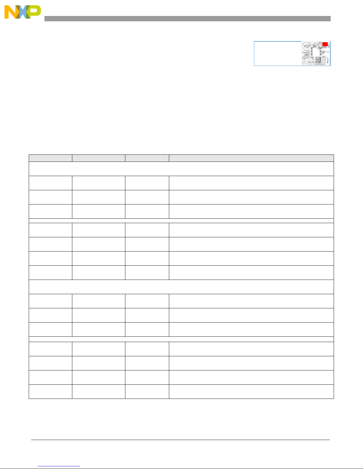
The FlexRay
interface is in the top
right corner of the
EVB on the top edge
6.6.
FlexRay (P2, P3, J1, J2, J3, J4)
The EVB incorporates two FlexRay TJA1080TS/N interfaces connected to MCU FlexRay channels A
and B and routed to two Molex 1.25mm pitch PicoBlade shrouded headers (standard on many Freescale
EVB’s). Jumpers are provided to disconnect the MCU signals from the FlexRay interface if required as
well as providing general configuration.
By default, all of the jumper headers are fitted which routes the MCU signals to the FlexRay physical
interface as well as configuring the controller for a default mode of operation (Transmitter enabled,
Receiver enabled, not in low power mode). Please consult the FlexRay transceiver and general FlexRay
specifications before changing any of the mode jumpers.
Table 15. FlexRay Configuration Jumpers (J1, J2, J3, J4)
MPC5748G EVB User Guide, User Guide, Rev. 0, 08/2015
22 Freescale Semiconductor, Inc.
Page 23
AV Interface Connectors
Important:
The EVB daughtercards are supplied with a 40 MHz crystal which is a requirement for FlexRay in
order to generate the correct clock timing. If you have changed the default crystal on the daughtercard
and wish to use FlexRay, you must ensure a 40 MHz crystal is fitted.
The SD socket is
mounted on the
underside of the
board in the top left
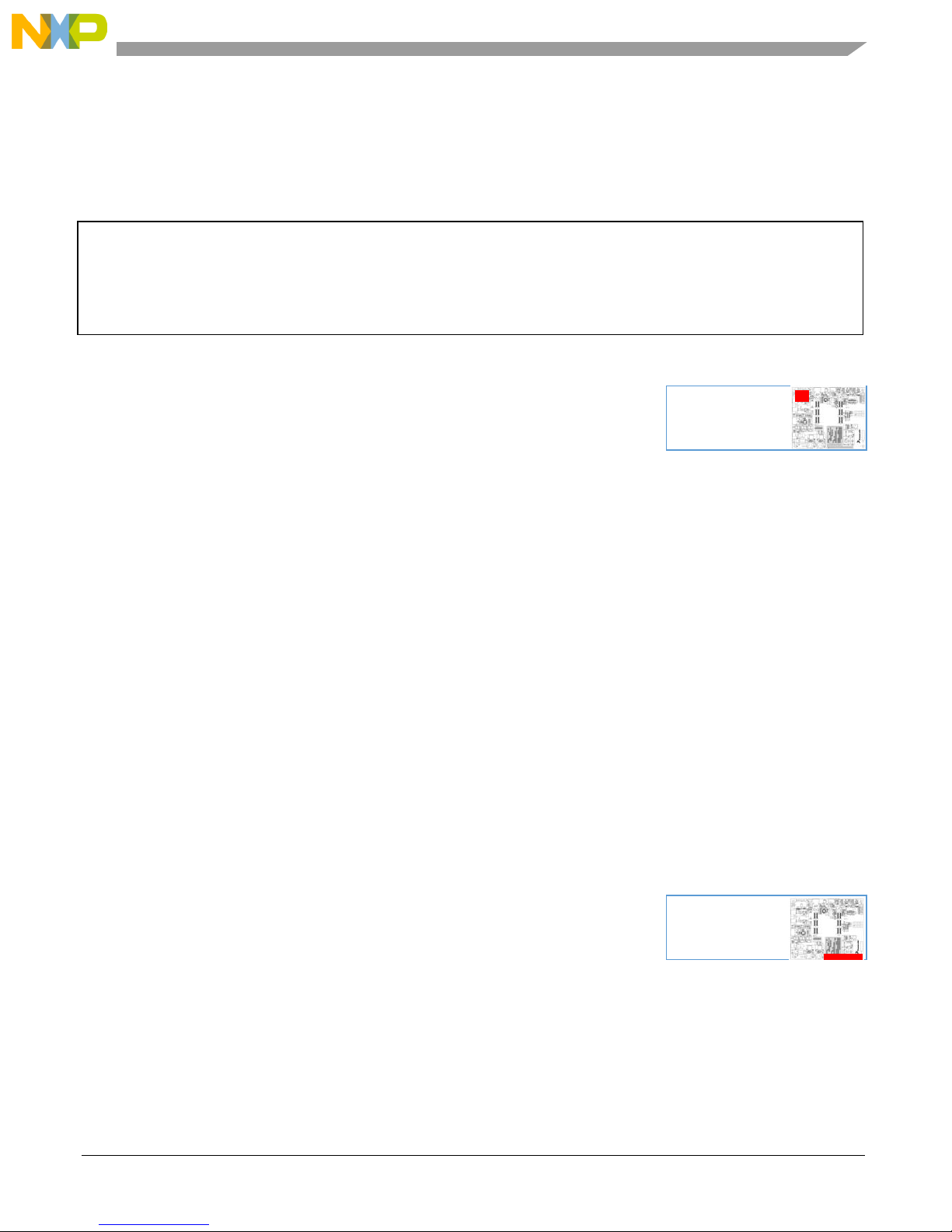
The SAI audio
connector is on the
bottom edge of the
EVB
The MCU FlexRay pins are powered from the VDD_HV_A domain, which is configured between 3.3V
and 5.0 V on the daughtercard using jumper J5. The FlexRay tranceivers I/O voltage pin is connected to
the PER_HVA net configured with jumper J24 on the main EVB. Care must be taken to ensure that the
MCU VDD_HV_A and PER_HVA supplies are the same when using the FlexRay transceiver.
6.7.
SD Card Socket (P200)
The EVB supports a 4-bit SD interface (note that MPC5748G supports 8-bit SD data) which is routed to
a full sized SD card connector on the underside of the EVB. There is no user configuration required.
The SD socket has hardware card detection (routed to PA0) and write protection (routed to PH8) status
outputs which will be grounded when active.
The MCU SD card signals are all in the VDD_HV_A domain. The SD card specification is for an
interface voltage of between 2.7V and 3.6V so the SD card can only be used when VDD_HV_A is set to
3.3V (PER_HVA has no impact on the voltage on the SD card)
CAUTION
If VDD_HV_A is set to 5V, damage may be caused to an SD card if an
attempt is made to access it in software. If you need to leave the SD card
in the socket with VDD_HV_A set to 5V, ensure all the SD card pads are
left as high impedance
7. AV Interface Connectors
This section details the Audio / Video interface connectors on the EVB. Each of these connectors can be
used to add additional daughtercards (not supplied) to add functionality.
7.1.
SAI Audio Connectors (P24, P25)
The EVB includes two 0.1” headers that can be used to interface to an SAI audio board (available
separately, please consult your Freescale representative). There is no EVB configuration required when
using these connectors other than to ensure the EVB is switched off prior to fitting or removing the
daughtercard.
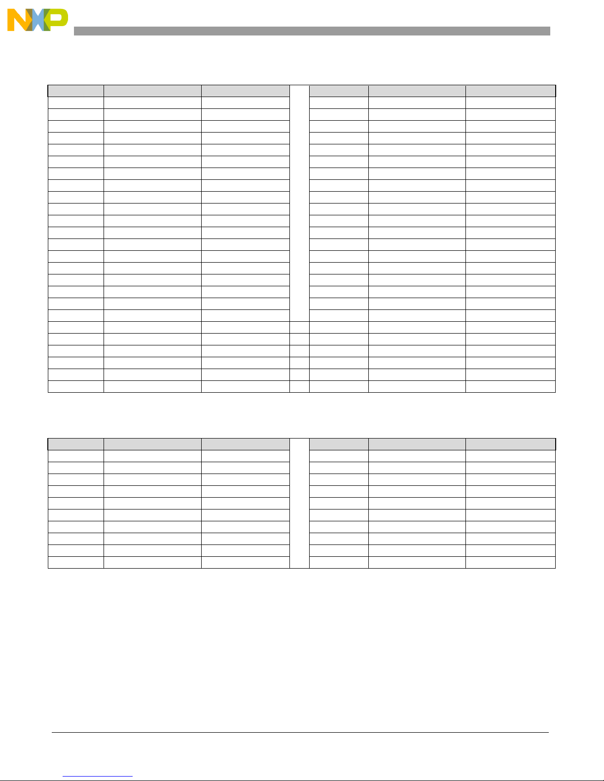
The pinout of the connectors is shown below for reference and these connectors can also be used for
GPIO connectivity
MPC5748G EVB User Guide, User Guide, Rev. 0, 08/2015
Freescale Semiconductor, Inc. 23
Page 24
Pin No
Function
Connection
Pin No
Function
Connection
1
3.3V
3V3_SR
2
GND
GND
3
SAI0_DATA3
PF2 4 GND
GND
5
SAI0_DATA2
PF3 6 GND
GND
7
SAI0_DATA1
PF4 8 GND
GND
9
SAI0_DATA0
PF5
10
GND
GND
11
SAI0_BCLK
PF1
12
GND
GND
13
SAI0_SYNC
PB10
14
GND
GND
15
SAI0_MCLK
PF0
16
GND
GND
17
eMIOS1_7H
PH5
18
GND
GND
19
I2C_SCL3
PE11
20
GND
GND
21
I2C_SDA3
PE10
22
GND
GND
23
SAI1_DATA0
PJ2
24
GND
GND
25
SAI1_BCLK
PJ3
26
GND
GND
27
eMIOS1_6H
PH4
28
GND
GND
29
SAI1_SYNC
PF6
30
GND
GND
31
SAI1_MCLK
PF7
32
GND
GND
33
I2C_SCL2
PE9
34
GND
GND
35
I2C_SDA2
PE8
36
GND
GND
37
SAI2_DATA0
PI14
38
GND
GND
39
SAI2_BCLK
PJ1
40
GND
GND
41
SAI2_SYNC
PJ0
42
GND
GND
43
SAI2_MCLK
PI15
44
GND
GND
45
eMIOS1_5H
PH3
46
GND
GND
47
GPIO Control
PA5
48
GND
GND
49
5.0V
5V0_SR
50
GND
GND
Pin No
Function
Connection
Pin No
Function
Connection
1
N/C
N/C 2 GND
GND
3
DSPI0_SIN
PA12
4
GND
GND
5
DSPI0_SOUT
PA13
6
GND
GND
7
DSPI0_SCK
PA14
8
GND
GND
9
DSPI0_SS0
PA15
10
GND
GND
11
DSPI3_SOUT
PG2
12
GND
GND
13
DSPI3_SS3
PG3
14
GND
GND
15
DSPI3_SCK
PG4
16
GND
GND
17
DSPI3_SIN
PG5
18
GND
GND
19
N/C
N/C
20
GND
GND
Table 16. 50-pin SAI Audio Daughtercard Connector P24
Table 17. 20-pin SAI Audio Daughtercard Connector P25
Note that connector P25 is not populated and must be fitted if required
CAUTION
Before the daughtercard is installed or removed, the EVB must be
powered OFF to prevent potential damage to the EVB or daughter card
components.
MPC5748G EVB User Guide, User Guide, Rev. 0, 08/2015
24 Freescale Semiconductor, Inc.
Page 25
AV Interface Connectors
Pin No
Function
Connection
Pin No
Function
Connection
1
5V
5V0_SR
2
3.3V
3V3_SR
3
GND
GND 4 3.3V
3V3_LR
5
GND
GND
6
GND
GND
7
GND
GND
8
ADC0
PD5
9
ADC1
PD6
10
GND
GND
11
GND
GND
12
ADC2
PD4
13
GND
GND
14
GND
GND
15
GND
GND
16
GND
GND
17
ID0
PD77
18
ID17
PD8
19
GND
GND
20
Pin No
Function
Connection
Pin No
Function
Connection
1
GND
GND 2 GND
GND
3
I2C0_SCL
PO0
4
I2C0_SDA
PO1 5 GND
GND 6 GND
GND
7
GND
GND 8 GND
GND
9
DSPI0_SIN
PA12
10
DSPI0_SOUT
PA13
11
DSPI0_SS0
PA15
12
DSPI0_SCK
PA14
13
GND
GND
14
GND
GND
15
GPIO0/IRQ
PK3
16
GPIO1
PK0
17
GPIO2
PK1
18
GPIO3
PK2
19
GPIO4
PK4
20
N/C
N/C
The TWRPI
connectors are at
the bottom right
hand corner
The MLB
daughtercard
connector is on the
RHS of the EVB
7.2.
TWRPI Connectors (P26, P27)
The EVB includes two fine pitch TWRPI headers that can be used to interface to an SAI audio board
(available separately, please consult your Freescale representative) along with the 0.1” headers
mentioned in the section above. There is no EVB configuration required when using these connectors
other than to ensure the EVB is switched off prior to fitting or removing the daughtercard. The pinout of
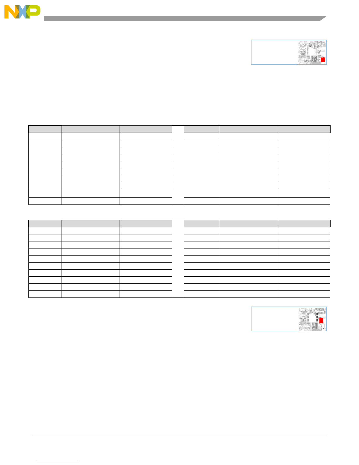
the connectors is shown below for reference.
Table 18. TWRPI Connector P26
Table 19. TWRPI Connector P27
7.3.
MLB Daughtercard Connector (P16)
There is a 40-pin interface connector on the EVB for connecting an MLB (Media Local Bus)
daughtercard. There is no hardware configuration possible at EVB level for this connector.
MLB Daughtercards are available direct from SMSC
As with all daughtercards, the EVB must be powered OFF to prevent damage to the EVB or daughter
card components.
7
ID0 and ID1 have a 10K pullup to 3V3
MPC5748G EVB User Guide, User Guide, Rev. 0, 08/2015
Freescale Semiconductor, Inc. 25
Page 26
The GPIO matrix is
on the bottom edge
of the EVB above
the SAI audio
8. User Interface (I/O)
This section details the user I/O available on the EVB and includes the GPIO matrix, switches, LED’s
and the ADC variable resistor.
8.1.
GPIO Matrix
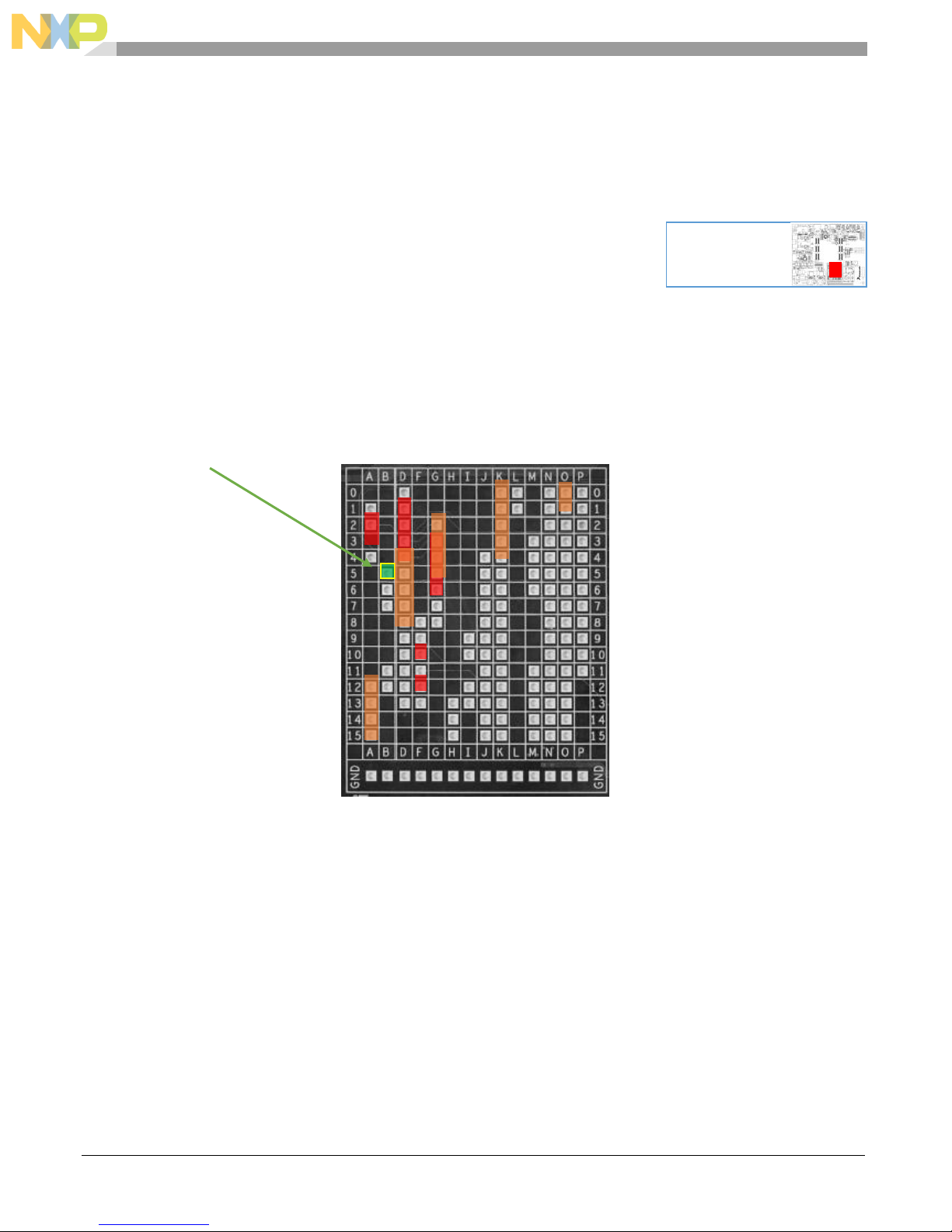
All of the available GPIO pins (those not already used for existing EVB peripherals) are available at the
GPIO matrix shown below. The matrix provides an easy to follow, intuitive, space saving grid of 0.1”
header through-hole pads. Users can solder wires, fit headers or simply insert a scope probe into the
respective pad.
To use the matrix, simply read the port letter from the top or bottom row of text then the pad number
from the columns on the left or right of the matrix. For example, the 1st pad available on Port B is PB5
as highlighted in green below.
If a pad is populated in the matrix, it means this is available for exclusive use as GPIO. The exception to
this are the port pins detailed below which are also shared with switches or user LED’s (shaded red in
the matrix diagram above).
PG2, PG3, PG4, PG5 – User LED’s 1..4
PD0, PD1, PD2, PD3 – HEX Encoder Switch
PA1,PA2, PF9, PF11 – User pushbutton Switches
In addition there are GPIO pins that are shared with the SAI Audio and TWRPI connectors as detailed
below and shaded orange. These are totally available unless the SAI / TWRPI headers are being used.
PA[12..15], PD[4..8], PG[2..5], PK[0..4], PO[0..1]
MPC5748G EVB User Guide, User Guide, Rev. 0, 08/2015
26 Freescale Semiconductor, Inc.
Figure 12. GPIO Matrix
Page 27
User Interface (I/O)
Switch
Number
MCU Pin
P18 Connection Pin
SW3
1
PA1
Pin1 (UpperMost)
SW4
2
PA2
Pin2
SW6
3
PF9
Pin3
SW7
4
PF11
Pin4
The user pushbutton
switches are in the
bottom left corner of
the EVB
8.2.
User Switches (SW3, SW4, SW6, SW7, P22)
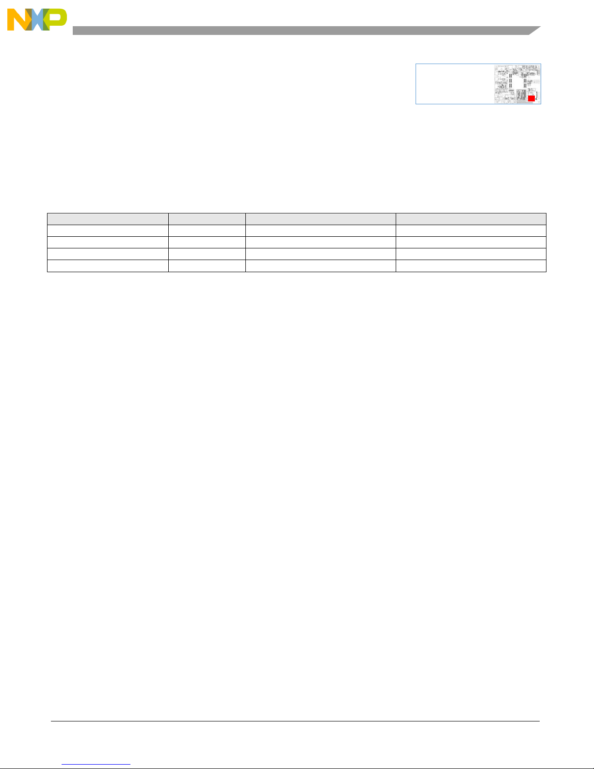
There are 4 active high (pulled low, driven to 3.3V) pushbutton switches (SW3, SW4, SW6, SW7)
connected to a 4 way header (P22) in a box titled “User Switches”. The switches are also directly
connected to MCU ports so no additional wiring is required unless you require to route these to a
different GPIO port.
The switches are connected as follows:
Table 20. User Pushbutton Switches (SW3, SW4, SW6, SW7)
NOTE
The MCU ports used on the user pushbutton switches are also routed to
the GPIO matrix.
There are zero ohm resistors on the direct connections between each
switch and the MCU pins. These can be removed if required to isolate the
switch from the respective MCU pin (useful if the switch is being
manually routed to another pin on the GPIO matrix).
MPC5748G EVB User Guide, User Guide, Rev. 0, 08/2015
Freescale Semiconductor, Inc. 27
Page 28
Position
HEX_SW4
(PD3, P20-4)
HEX_SW3
(PD2, P20-3)
HEX_SW2
(PD1, P20-2)
HEX_SW1
(PD0, P20-1)
0 0 0 0 0 1 0 0 0
1
2
0
0 1 0 3 0 0 1
1 4 0 1 0
0 5 0 1 0
1 6 0 1 1
0 7 0 1 1
1
8
1
0 0 0 9 1 0 0
1
A
1
0 1 0
B
1
0 1 1
C
1
1 0 0
D
1
1 0 1
E
1
1 1 0
F
1
1 1 1
Jumper
Position
PCB Legend
Description
J26
(3V3)
FITTED (D)
The hex encoder switch is powered with 3.3V (functional)
Removed
The hex encoder switch is not powered and will not drive outputs
The hex encoder
switch is located
above the user
pushbutton switches
8.3.
Hex Encoder Switch (SW2, J26, P20)
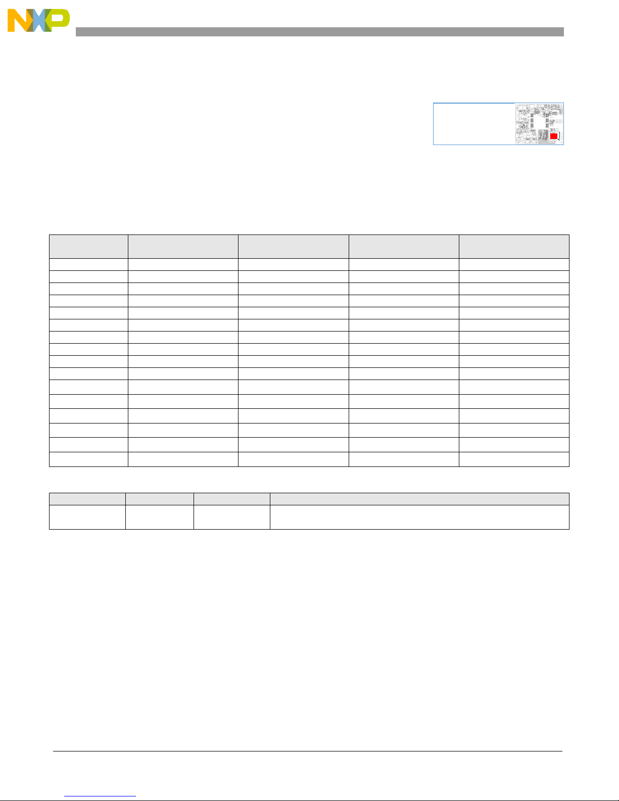
There is a single hex encoded 16 position rotary switch on the EVB. This outputs a binary encoded hex
value (active high) on 4 MCU ports (Port D[0..3]) as well as a 4 pin header P20. There is a jumper J26
which can be used to isolate the supply to the hex encoder if required. This prevents any voltage being
asserted on the MCU pins irrespective of the position of the switch
Table 21. Hex Encoder Switch (SW2)
Table 22. Hex Encoder Switch Power Jumper (J26)
The MCU ports used on the user pushbutton switches are also routed to
the GPIO matrix.
There are zero ohm resistors on the direct connections between the switch
output and the MCU pins. These can be removed if required to isolate the
switch from the respective MCU pin (useful if the switch is being
manually routed to another pin on the GPIO matrix).
MPC5748G EVB User Guide, User Guide, Rev. 0, 08/2015
28 Freescale Semiconductor, Inc.
NOTE
Page 29
User Interface (I/O)
Switch
Number
MCU Pin
P19 Connection Pin
DS2
1
PG2
Pin1 (Upper Pin)
DS3
2
PG3
Pin2
DS7
3
PG4
Pin3
DS8
4
PG5
Pin4
Jumper
Position
PCB Legend
Description
J17
FITTED (D)
Output from RV1 is routed to MCU PB4 pin
Removed
MCU PB4 is not connected to RV1
The user LED’s are
above the user
switches in the lower
right quarter
The ADC Pot is to
the right of the user
LED’s in the lower
right corner
8.4.
User LED’s (DS2, DS3, DS7, DS8, P19)
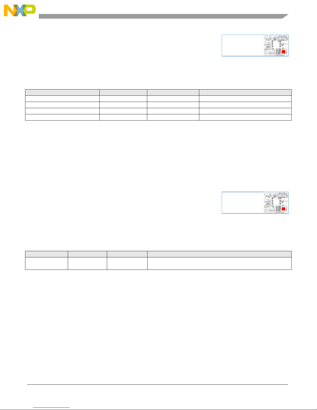
There are four active low user LED’s connected directly to 4 MCU ports (PG[2..5]) as well as to a 4 pin
header.
Table 23. User LEDs (DS2, DS3, DS7, DS8, P19)
NOTE
The MCU ports used on the LEDs are also routed to the GPIO matrix.
There are zero ohm resistors on the direct connections between each LED
and the MCU pins. These can be removed if required to isolate the LED
from the respective MCU pin (useful if the LED is being manually routed
to another pin on the GPIO matrix).
8.5.
ADC Input Potentiometer (J17, RV1)
There is a small variable resistor RV1 on the EVB which routes a voltage between 0v and 3.3V to MCU
pin PB4. This is useful for quick ADC testing. Jumper J17 which is fitted by default can be removed to
disconnect MCU PB4 from RV1 if desired.
Table 24. ADC Input Potentiometer Enable (J19)
There is also a test point TP18 connected to the variable resistor output for monitoring purposes.
MPC5748G EVB User Guide, User Guide, Rev. 0, 08/2015
Freescale Semiconductor, Inc. 29
Page 30
No
PortA
PortB
PortC
PortD
PortE
PortF
PortG
PortH
0
SD Card
CAN0
JTAG
GPIO 3
MLB
SAI Audio
Ethernet
Ethernet
1
GPIO 2
CAN0
JTAG
GPIO 3
MLB
SAI Audio
Ethernet
Ethernet
2
GPIO 2
LIN0
USB1
GPIO 3
FlexA
SAI Audio
GPIO
4, 5
Ethernet
3
Ethernet
LIN0
USB1
GPIO 3
FlexA
SAI Audio
GPIO
4 , 5
SAI Audio
4
GPIO
ADC Pot
FlexB
GPIO 5
FlexB
SAI Audio
GPIO
4, 5
SAI Audio
5
SAI Audio
GPIO
FlexA
GPIO 5
FlexB
SAI Audio
GPIO
4 , 5
SAI Audio
6
MLB
GPIO
LIN1
GPIO 5
SD Card
SAI Audio
GPIO
MLB
7
Ethernet
GPIO
LIN1
GPIO 5
SD Card
SAI Audio
GPIO
MLB
8
Ethernet
EXTAL32
RS232
GPIO 5
SAI Audio
GPIO
GPIO
SD Card
9
Ethernet
XTAL32
RS232
GPIO
SAI Audio
GPIO 2
MLB
JTAG
10
Ethernet
SAI Audio
CAN1
GPIO
SAI Audio
GPIO
USB1
JTAG
11
Ethernet
GPIO
CAN1
GPIO
SAI Audio
GPIO 2
USB1
USB1
12
GPIO 5
GPIO
Flex
GPIO
Ethernet
GPIO
Ethernet
USB1
13
GPIO 5
MLB
Flex
GPIO 1
Ethernet
GPIO
Ethernet
GPIO
14
GPIO 5
MLB
Flex
MLB
USB1
Ethernet
USB1
GPIO
15
GPIO 5
MLB
Flex
MLB
USB1
Ethernet
USB1
GPIO
No
PortI
PortJ
PortK
PortL
PortM
PortN
PortO
PortP
PortQ
0
SD Card
SAI Audio
GPIO 5
GPIO
NEXUS
GPIO
GPIO 5
GPIO
USB0
1
SD Card
SAI Audio
GPIO 5
GPIO
NEXUS
GPIO
GPIO 5
GPIO
USB0
2
SD Card
SAI Audio
GPIO 5
NEXUS
NEXUS
GPIO
GPIO
GPIO
USB0
3
SD Card
SD Card
GPIO 5
NEXUS
GPIO
GPIO
GPIO
GPIO
USB0
4
USB1
GPIO
GPIO 5
NEXUS
GPIO
GPIO
GPIO
GPIO
USB0
5
USB1
GPIO
GPIO
NEXUS
GPIO
GPIO
GPIO
GPIO
USB0
6
USB0
GPIO
GPIO
NEXUS
GPIO
GPIO
GPIO
GPIO
USB0
7
USB1
GPIO
GPIO
NEXUS
NEXUS
GPIO
GPIO
GPIO
USB0
8
MLB
GPIO
GPIO
JTAG
NEXUS
GPIO
GPIO
GPIO
-
9
GPIO
GPIO
GPIO
NEXUS
NEXUS
GPIO
GPIO
GPIO
-
10
GPIO
GPIO
GPIO
NEXUS
NEXUS
GPIO
GPIO
GPIO
-
11
Ethernet
GPIO
GPIO
NEXUS
GPIO
GPIO
GPIO
GPIO
-
12
GPIO 1
GPIO
GPIO
NEXUS
GPIO
GPIO
GPIO
USB0
-
13
GPIO 1
GPIO
GPIO
NEXUS
GPIO
GPIO
GPIO
USB0
-
14
SAI Audio
GPIO
GPIO
NEXUS
GPIO
GPIO
GPIO
USB0
-
15
SAI Audio
GPIO
GPIO
NEXUS
GPIO
GPIO
GPIO
USB0
-
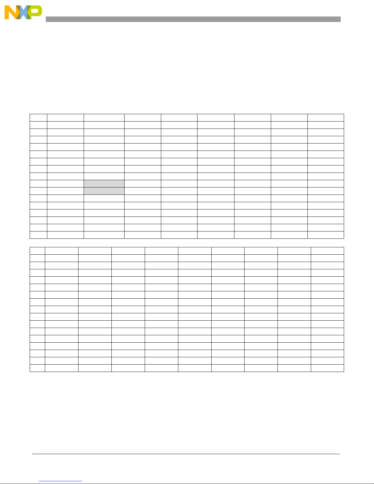
9. MCU Port Pin EVB Functions
The table below shows what each MCU pin is used for on the EVB. Note that not all MCU pins will be
available depending on the device package being used.
Table 25. Port Pin Functions
1
Shared with MLB header (via no populated zero ohm resistors)
2
Shared with user switches
3
Shared with Hex Encoder Switch
4
Shared with user LED’s
5
Shared with TWRPI (P26, P27) or SAI Audio P25
MPC5748G EVB User Guide, User Guide, Rev. 0, 08/2015
30 Freescale Semiconductor, Inc.
Page 31
Default Jumper Summary Table
Jumper
Default
Posn
PCB
Legend
Description
J1 Posn 1-2
Fitted (D)
BGE
FlexRay B PHY Bus Guardian Enable (Transmitter is enabled)
J1 Posn 3-4
Fitted (D)
EN
FlexRay B PHY is enabled
J1 Posn 5-6
Fitted (D)
STBN
FlexRay B PHY will not enter Standby Mode
J1 Posn 7-8
Fitted (D)
WAKE
FlexRay B PHY Wakeup signal pulled low
J2 Posn 1-2
Fitted (D)
BGE
FlexRay A PHY Bus Guardian Enable (Transmitter is enabled)
J2 Posn 3-4
Fitted (D)
EN
FlexRay A PHY is enabled
J2 Posn 5-6
Fitted (D)
STBN
FlexRay A PHY will not enter Standby Mode
J2 Posn 7-8
Fitted (D)
WAKE
FlexRay A PHY Wakeup signal pulled low
J3 Posn 1-2
Fitted (D)
TX
MCU PC5 is connected to FlexRay A transceiver TX
J3 Posn 3-4
Fitted (D)
TXEN
MCU PE2 is connected to FlexRay A transceiver TXEN
J3 Posn 5-6
Fitted (D)
RX
MCU PE3 is connected to FlexRay A transceiver RX
J4 Posn 1-2
Fitted (D)
TX
MCU PE4 is connected to FlexRay B transceiver TX
J4 Posn 3-4
Fitted (D)
TXEN
MCU PC4 is connected to FlexRay B transceiver TXEN
J4 Posn 5-6
Fitted (D)
RX
MCU PE5 is connected to FlexRay B transceiver RX
J5
1-2 (D)
MII
Ethernet PHY is configured in MII mode
J6 (X1)
1-2 (D)
Ethernet PHY X2 clock is connected to 25MHz xtal
J7 (X2)
1-2 (D)
Ethernet PHY X1 clock is connected to 25MHz xtal
J8 (RST)
1-2 (D)
NORM
The Ethernet PHY will be reset along with MCU reset
J9 (EN)
Fitted (D)
Reset from reset switch and debug connectors is active
J10 (LIN0) 1-2
Fitted (D)
RX
MCU LIN0_RX signal (PB3) is routed to LIN0 interface
J10 (LIN0) 3-4
Fitted (D)
TX
MCU LIN0_TX signal (PB2) is routed to LIN0 interface
J11 (Master_EN)
Fitted (D)
LIN0 is configured in Master Mode
J12 (LIN1) 1-2
Fitted (D)
RX
MCU LIN1_TX signal (PC7) is routed to LIN1 interface
J12 (LIN1) 3-4
Fitted (D)
TX
MCU LIN1_RX signal (PC6) is routed to LIN interface
J13 (Master_EN)
Fitted (D)
LIN1 is configured in Master Mode
J14 (CAN1) 1-2
Fitted (D)
TX
MCU CAN1_TX signal (PC10) is routed to CAN interface
J14 (CAN1) 3-4
Fitted (D)
RX
MCU CAN1_RX signal (PC11) is routed to CAN interface
J15 (CAN0) 1-2
Fitted (D)
TX
MCU CAN0_TX signal (PB0) is routed to CAN interface
J15 (CAN0) 3-4
Fitted (D)
RX
MCU CAN0_RX signal (PB1) is routed to CAN interface
J16 Posn 1-2
Fitted (D)
RX
MCU LIN2_RX signal (PC9) is routed to the FTDI interface
J16 Posn 3-4
Fitted (D)
TX
MCU LIN2_TX signal (PC8) is routed to the FTDI interface
J17
Fitted (D)
Output from RV1 is routed to MCU PB4 pin
J18 (1V25L)
Fitted (D)
1.25V Linear regulator output is routed to daughter card
J19 (5V0S)
Fitted (D)
5.0V Switching regulator output is routed to daughter card
J20 (3V3L)
Fitted (D)
3.3V Linear regulator output is routed to daughter card
J21 (5V0L)
Fitted (D)
5.0V Linear regulator output is routed to daughter card
J22 (3V3S)
Fitted (D)
3.3V Switching regulator output is routed to daughter card
J23 (INPUT SEL)
1-2 (D)
12V
1.25V Linear regulator is powered from main 12V
J24 (HVA)
1-2 (D)
3V3
EVB peripherals in HVA domain are set to use I/O voltage of 3.3V
J25 (HVB)
1-2 (D)
3V3
EVB peripherals in HVB domain are set to use I/O voltage of 3.3V
J26 (3V3)
Fitted (D)
The hex encoder switch is powered with 3.3V (functional)
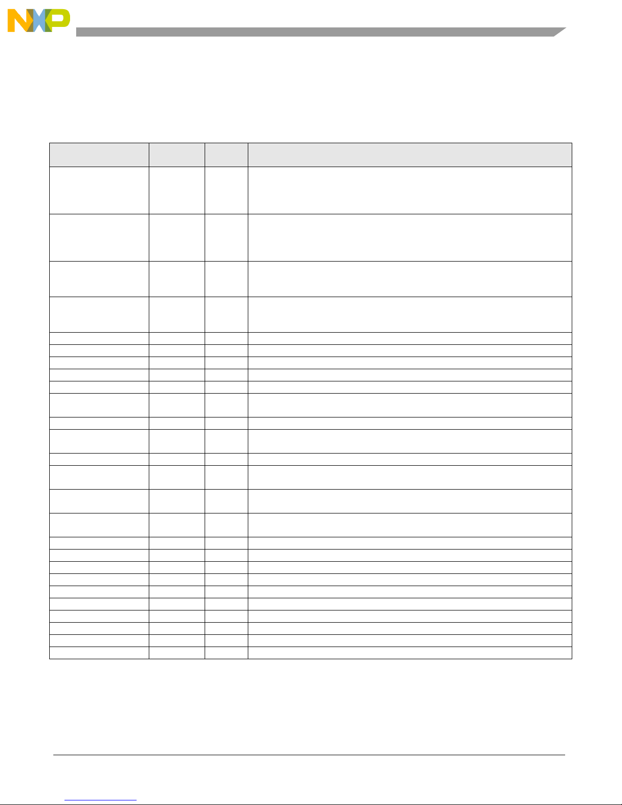
10. Default Jumper Summary Table
The following tables detail the default (D) jumper configuration of the EVB and daughtercards
Table 26. Default Jumper Positions (Main Board)
MPC5748G EVB User Guide, User Guide, Rev. 0, 08/2015
Freescale Semiconductor, Inc. 31
Page 32
Jumper
Default
Posn
PCB
Legend
Description
1 (XTAL)
1-2 (D)
Y1
MCU XTAL signal is routed to crystal Y1
J2 (EXTAL)
1-2 (D)
Y1
MCU EXTAL signal is routed to crystal Y1
J3 (ADC0)
1-2 (D)
3V3
MCU ADC0 pin is connected to 3.3V (Linear)
J4 (ADC1)
1-2 (D)
3V3
MCU ADC1 pin is connected to 3.3V (Linear)
J5 (HVA)
1-2 (D)
3V3
MCU VDD_HV_A domain is connected to 3.3V (Switching Regulator)
J6 (HVB)
1-2 (D)
3V3
MCU VDD_HV_B domain is connected to 3.3V (Switching Regulator)
J7 (HVC)
1-2 (D)
3V3
MCU VDD_HV_C domain is connected to 3.3V (Switching Regulator)
J8 (FLA )
Fitted (D)
MCU VDD_HV_FLA pin is connected to 3.3v (Switching Regulator)
J9 (REG)
1-2 (D)
3V3
MCU ballast transistor collector is connected to 3.3V (Switching)
J10 (VDDLV)
1-2 (D)
REG
MCU VDD_LV domain is powered from ballast transistor
J11 (DAC)
1-2 (D)
HVA
MCU VIN1_CMP_REF is powered from VDD_HV_A
J12
Fitted (D)
Ballast collector supply is enabled (jumper can be used for current measure)
J13
1-2 (D)
** Only valid on certain devices – External Ballast enabled.
Table 27. Default Jumper Positions (Daughtercards)
Note that not all jumpers will be present on all of the daughtercards.
MPC5748G EVB User Guide, User Guide, Rev. 0, 08/2015
32 Freescale Semiconductor, Inc.
Page 33
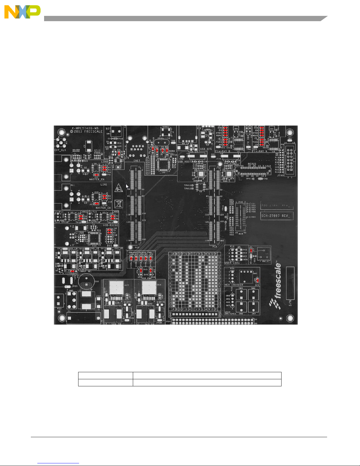
Default Jumper Diagram
Date
Substantial changes
August 2015
Initial release
11. Default Jumper Diagram
The diagram below shows the location and configuration of the default jumpers of the main board and
provides an easy to use cross reference. By default all of the jumpers are fitted to the daughtercard (3
way jumpers in position 1-2).
NOTE
Following figure is of an older board revision however there were no
additional jumpers and no jumpers have moved position.
12. Revision History
MPC5748G EVB User Guide, User Guide, Rev. 0, 08/2015
Freescale Semiconductor, Inc. 33
Figure 13. Default Jumper Position
Page 34

13. Appendix
The following EVB schematics are detailed in the following sections:
Main EVB (motherboards)
324BGA Daughtercard
256BGA Daughtercard
176QFP Daughtercard
100QFP Daughtercard (MPC5746C only)
MPC5748G EVB User Guide, User Guide, Rev. 0, 08/2015
34 Freescale Semiconductor, Inc.
Page 35

Main EVB
Page 36
5
5
4
4
3
3
2
2
1
1
D D
C C
B B
A A
X5
Freescale AISG Applications, East Kilbride
X6
X2
X3
X4
Audio - SAI Audio. AVB and TWRPI headers
Revision Information
0.1
Designer
Alasdair Robertson
CommentsRev Date
Power - Switching voltage regulators
Reset and External Clock Input
Sheet 8
Sheet 9
Sheet 10
Sheet 11
Sheet 12
Sheet 13
Sheet 14
Sheet 15
Sheet 16
These schematics are provided for reference purposes only. As such,
Freescale does not make any warranty, implied or otherwise, as to the
suitability of circuit design or component selection (type or value) used in
these schematics for hardware design using the Freescale MPC574xG family
of Microprocessors. Customers using any part of these schematics as a
basis for hardware design, do so at their own risk and Freescale does not
assume any liability for such a hardware design.
Sheet 2
Sheet 3
Sheet 4
Sheet 5
Sheet 6
Sheet 7Comms - CAN and LIN
Comms - Ethernet
Comms - USB Interfaces
Memory - SD Card Slot
AV - MOST Interface
User notes are given throughtout the schematics.
Specific PCB LAYOUT notes are detailed in ITALICS
Caution:
19 Feb 2012
Comms - RS232 (USB FTDI interface)
Comms - FlexRAY
User - Switches, LED's and Potentiometer
User - GPIO Pin Matrix
Table Of Contents:
Notes:
MPC574xx Customer Evaluation Board (X-MPC574XG-MB)
- All components and board processes are to be ROHS compliant
- All small capacitors are 0402 unless otherwise stated
- All resistors are 0603 5% 0.1w unless otherwise stated. All zero ohm links are 0603
- All connectors and headers are denoted Px and are 2.54mm pitch unless otherwise stated
- All jumpers are denoted Jx. Jumpers are 2mm pitch
- Jumper default positions are shown in the schematics. For 3 way jumpers, default is always posn 1-2.
2 Pin jumpers generally have the "source" on pin 1.
- All switches are denoted SWx
- All test points (SMT wire loop style) are denoted TPx
- Test point Vias (just through hole pads) are denoted TPVx
X1
Power - Main input and Linear voltage regulators
Daughter Card Connectors (Sockets)
JTAG and Nexus Connectors
Start of capture, Working version01 Feb 2012
1st release for internal review (Complete Board)
28 Feb 2012
Alasdair Robertson
Alasdair Robertson 2nd release for internal review (split into main board and DC)
Signals (ports) have not been routed via busses as this makes it harder to determine where each signal goes.
Alasdair Robertson
Version sent to Pre Layout, incorporating fixes from review
Final review (including new USB transceiver)11 Mar 2013
Alasdair Robertson13 Mar 2013
14 Mar 2013 Alasdair Robertson Component consolodation, Few minor changes. Sent to Layout
3 Different test points used in design:
TPVx - Through Hole Pad small
TPHx - Through Hile Pad Large (for standard 0.1" header).
Also used on IO Matrix (IOMx)
TPX - Surface Mount Wire Loop
29 Mar 2013 Alasdair Robertson Changes made during layout to Daughtercard Connectors
A Post Layout (Back Annotated). Matches PCB RevAAlasdair Robertson
02 Apr 2013 Alasdair Robertson LAY RefDes Resequence and SCH BackAnnotateX7
17 Apr 2013
AX1 24 Jun 2013 Alasdair Robertson Fixes and changes to RevA Prototype design
AX2 10 July 2013 Alasdair Robertson Added CAN Term (DNP)
AX3 12 July 2013 Alasdair Robertson Corrected ground on ADC Pot
B 12 July 2013 Alasdair Robertson Production Release
BX1 20 Aug 2013 Alasdair Robertson Change to Ethernet 50MHz clock control
C 20 Aug 2013 Alasdair Robertson Production Release
CX1 18 Dec 2013 Alasdair Robertson CAN transceivers -> MC33901, ENET clock in RMII mode
CX2 05 May 2014 Alasdair Robertson Added comment about LM1117 VREG output
CX3 25 June 2014 Alasdair Robertson PH3..5 now GPIO matrix (was SAI), PM4, PD13, PM3 to SAI
CX4 26 June 2014 Alasdair Robertson Minor changes made during layout (no component changes)
CX5 26 June 2014 Alasdair Robertson Part Manager Tidy up
CX6 18 Aug 2014 Alasdair Robertson Added additional connector with DSPI Signals for AVB
CX7 03 Sept 2014 Alasdair Robertson Added additional TWRPI header (Sheet 12)
D 24 Sept 2014 Alasdair Robertson Released to Production (RevD PCB)
D1 14 Aug 2015 Alasdair Robertson Tidy up Schematics for UM (RevD PCB)
Drawing Title:
Size Document Number Rev
Date: Sheet
of
Page Title:
Designer:
Drawn by:
Approved:
Automotive Microcontroller Applications
East Kilbride, Scotland
This document contains information proprietary to Freescale and shall not be used for engineering design,
procurement or manufacture in whole or in part without the express written permission of Freescale
SCH-27897 PDF: SPF-27897 D1
MPC574xx Customer EVB Main Board
B
Friday, August 14, 2015
Index and Title Page
A. Robertson
A. Robertson
A. Robertson
116
Freescale General Business Use
Drawing Title:
Size Document Number Rev
Date: Sheet
of
Page Title:
Designer:
Drawn by:
Approved:
Automotive Microcontroller Applications
East Kilbride, Scotland
This document contains information proprietary to Freescale and shall not be used for engineering design,
procurement or manufacture in whole or in part without the express written permission of Freescale
SCH-27897 PDF: SPF-27897 D1
MPC574xx Customer EVB Main Board
B
Friday, August 14, 2015
Index and Title Page
A. Robertson
A. Robertson
A. Robertson
116
Freescale General Business Use
Drawing Title:
Size Document Number Rev
Date: Sheet
of
Page Title:
Designer:
Drawn by:
Approved:
Automotive Microcontroller Applications
East Kilbride, Scotland
This document contains information proprietary to Freescale and shall not be used for engineering design,
procurement or manufacture in whole or in part without the express written permission of Freescale
SCH-27897 PDF: SPF-27897 D1
MPC574xx Customer EVB Main Board
B
Friday, August 14, 2015
Index and Title Page
A. Robertson
A. Robertson
A. Robertson
116
Freescale General Business Use
Page 37
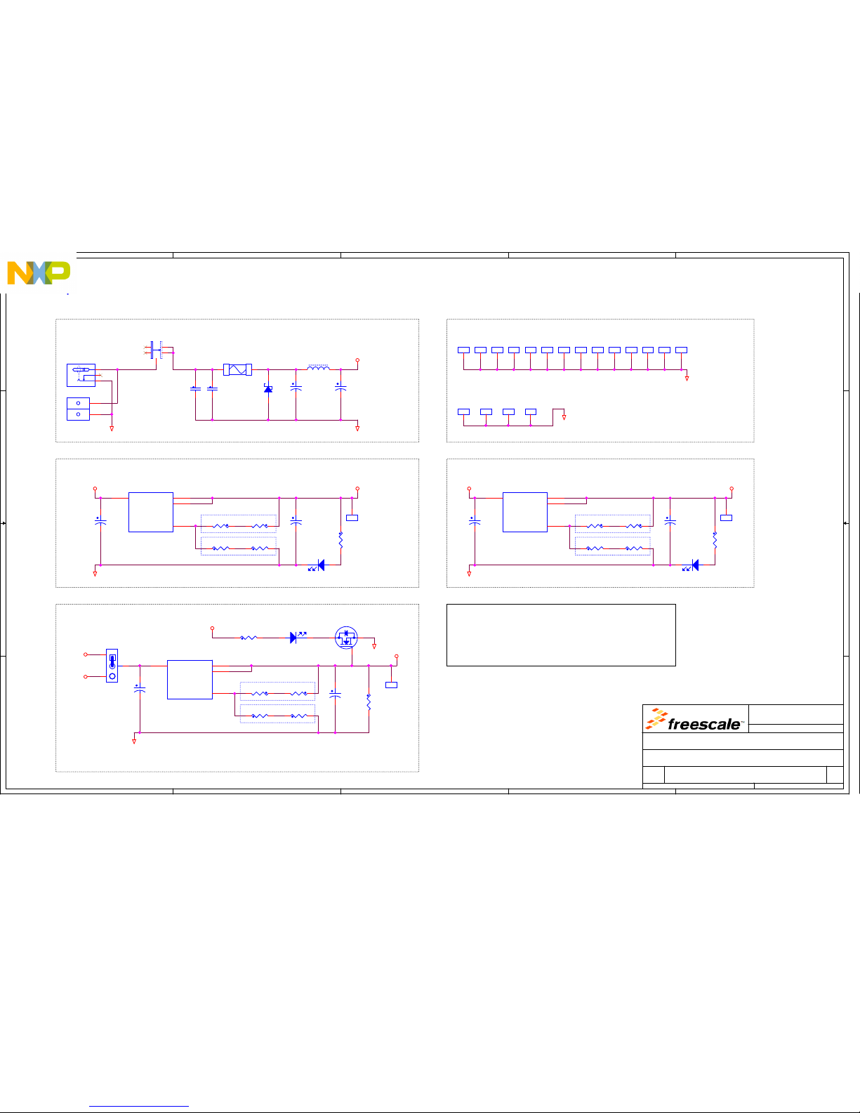
5
5
4
4
3
3
2
2
1
1
D D
C C
B B
A A
Rfb1
Rfb2
Main EVB
Power In
Vout = 1.25(1 + (R2/R1))
= 5.0V
(0603
50V)
GND Test Points, Top Side
Rfb1
Rfb2
Vout = 1.25(1 + (R2/R1))
= 3.295V
3.3V Linear Regulator (800mA Max **)
(35V TANT)(35V
TANT)
(0402 50V)
Could also use 2x82 Ohm resistors for RFB2 but not in agile...
1% resitors1% resitors
Rfb1
Rfb2
Vout = 1.25(1 + (R2/R1))
= 1.25V
1% resitors
1.25V Linear Regulator (800mA Max **)
(35V TANT)
(35V
TANT)
Power Input and Linear Voltage Regulators
Input 12V DC nominal (range 10v - 14v)
See note on schematic sheet 3 regarding 3.3V regulator when running at < 11V)
1.25V for External core supply. Simpler to use linear rather than switcher so can safely
power from 5V switcher (slight ripple not an issue) for reduced heat dissipation
(c200 rad
pol 50V)
2.1mm Barrel
Connector
(2 Screw
Connector)
(Power Switch)
Power Supply Input and Filter Test and reference points
GND Test Points for underside of board
5.0V Linear Regulator (800mA Max **)
(35V TANT)(35V
TANT)
(CC7343-43
25V)
(10v-14v)
(3A)
(3A)
1K Load
resistor to
ensure proper
regulation if
1.25V MCU
jumper removed
The LM1117 linear regulators provide a maximum output
current of 800mA in ideal conditions. The current
requirement for each regulator is in the region of 10's
of mA (significantly under the maximum rating) so
these regulators will run cool on the EVB.
** Notes on Linear Regulator LM1117
VFused12V-IN VSwitched
3V3_LRP12V
GND
1V25_LR
GND
P12V
5V0_SR
GND
P12V
GND
GND
GND
5V0_LRP12V
GND
GND
P12V
Drawing Title:
Size Document Number Rev
Date: Sheet
of
Page Title:
Automotive Microcontroller
Applications
East Kilbride, Scotland
SCH-27897 PDF: SPF-27897 D1
MPC574xx Customer EVB Main Board
B
Friday, August 14, 2015
Power Input and Linear Voltage Regulators
216
Freescale General Business Use
Drawing Title:
Size Document Number Rev
Date: Sheet of
Page Title:
Automotive Microcontroller
Applications
East Kilbride, Scotland
SCH-27897 PDF: SPF-27897 D1
MPC574xx Customer EVB Main Board
B
Friday, August 14, 2015
Power Input and Linear Voltage Regulators
216
Freescale General Business Use
Drawing Title:
Size Document Number Rev
Date: Sheet of
Page Title:
Automotive Microcontroller
Applications
East Kilbride, Scotland
SCH-27897 PDF: SPF-27897 D1
MPC574xx Customer EVB Main Board
B
Friday, August 14, 2015
Power Input and Linear Voltage Regulators
216
Freescale General Business Use
DS6
LED GREEN
AC
R305
1K
GND13
1
GND4
1
C268
0.1UF
TP17
1
L5
27uH
1 2
F1
Fuse Holder
1 2
GND10
1
R77 0
R72
100
DNP
GND17
1
GND7
1
GND1
1
+
C27
10UF
R73
100
U16
LM1117MPX-ADJ
ADJ
1
VOUT
2
IN3TAB_VOUT
4
R273
270
GND5
1
P23
A
1
B
2
+
C26
10UF
U15
LM1117MPX-ADJ
ADJ
1
VOUT
2
IN3TAB_VOUT
4
GND8
1
+
C30
10UF
DS5
LED GREEN
AC
R76 0
GND12
1
+
C32
1000UF
GND2
1
DS4
LED GREEN
A C
GND15
1
+
C29
10UF
C269
1000pF
R74
100
P21
1
3
2
R271 5.6
GND3
1
R284
0
+
C33
68UF
R75 0
DNP
SW5
1 3
4 2
5
R272
0
R70 300
GND11
1
+
C28
10UF
GND9
1
TP16
1
GND14
1
TP15
1
D202
B340A
A C
R274
560
U14
LM1117MPX-ADJ
ADJ
1
VOUT
2
IN3TAB_VOUT
4
GND6
1
J23
1
2
3
GND16
1
R285
0
GND18
1
Q1
BSH103
1
23
R71
158
+
C31
10UF
R283 1.8K
Page 38
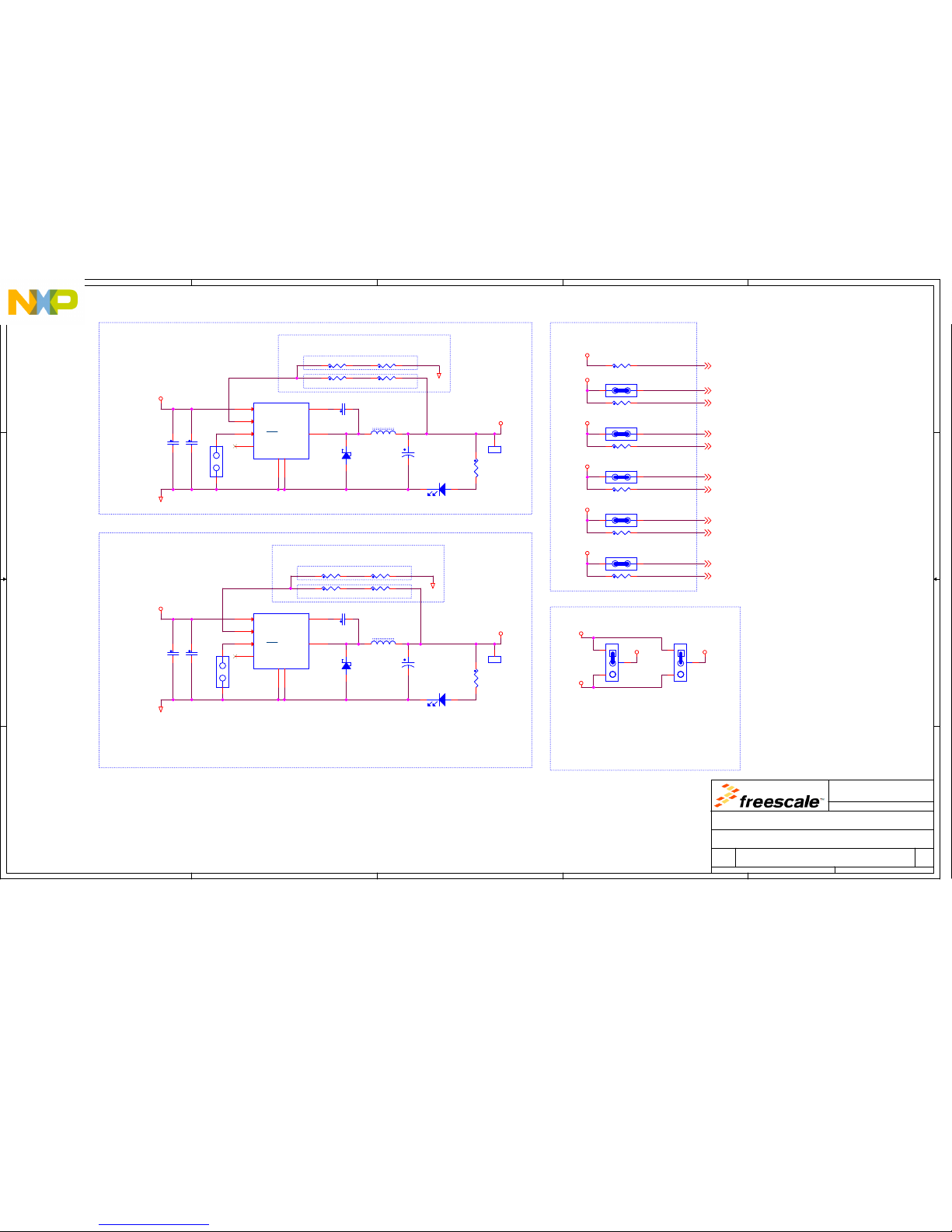
5
5
4
4
3
3
2
2
1
1
D D
C C
B B
A A
Design requires
B220A-13-F
diode. Use3A
version to
reduce no of
components
(12v input, 2.0A Output, 89% Efficient, 11.24w)
Switching Voltage Regulators and Supply Jumpers
5.0v Switching Regulator
(1210
25V)
(0603
50V)
(0603 50V)
(All Resistors 1% 0603_CC)
Rfb1
Rfb2
Vout = 1.21(1 + Rfb2/Rfb1) = 4.98V
APXE100ARA151MF80G
(1210
25V)
APXE100ARA151MF80G
(0603
50V)
3.3v Switching Regulator
(12v input, 2A Output, 83% Efficient)
(0603 50V)
(All Resistors 1% 0603_CC)
Rfb1
Rfb2
Vout = 1.21(1 + Rfb2/Rfb1) = 3.3V
Using Adjustable version of LM2676 rather than fixed 3.3V /
5V regulators to reduce number of components in BOM.
Where possible, components have been shared accross the
regulator designs to further reduce component count.
The 3.3v regulator design is optimised for an input voltage of 12V. If
the input voltage drops below approx 11V, the 3.3v output voltage
ripple may increase. This can be reduced by increasing the bulk storage
capacitor if required.
Caution
Global MCU Daughtercard
Supply Jumpers and DC power
Peripheral Power Control
These jumpers control the voltage of the
peripherals connected to MCU pads in the
VDD_HV_A / HV_B domains and are required
so the respective jumpers at the MCU can
be used for MCU current measurement.
The settings on these jumpers must
mirror the setting of the respective
MCU VDD_HV_A / HB_V jumpers
To Daughtercard
Connectors
MCU_3V3_S
MCU_5V0_S
MCU_3V3_L
MCU_5V0_L
MCU_1V25_L
DC_5V0_S
DC_3V3_S
DC_5V0_L
DC_3V3_L
DC_1V25_L
DC_P12V
P12V
GND
5V0_SR
GND
GND
3V3_SR
P12V
GND
3V3_SR
5V0_SR
3V3_LR
5V0_LR
1V25_LR
5V0_SR
3V3_SR
PER_HVA PER_HVB
P12V
DC_5V0_S
4
DC_3V3_S
4
DC_5V0_L
4
DC_3V3_L
4
DC_1V25_L
4
DC_P12V
4
MCU_1V25_L
4
MCU_5V0_S
4
MCU_5V0_L
4
MCU_3V3_S
4
MCU_3V3_L
4
Drawing Title:
Size Document Number Rev
Date: Sheet
of
Page Title:
Automotive Microcontroller
Applications
East Kilbride, Scotland
SCH-27897 PDF: SPF-27897 D1
MPC574xx Customer EVB Main Board
B
Friday, August 14, 2015
Switching Voltage Regulators
316
Freescale General Business Use
Drawing Title:
Size Document Number Rev
Date: Sheet of
Page Title:
Automotive Microcontroller
Applications
East Kilbride, Scotland
SCH-27897 PDF: SPF-27897 D1
MPC574xx Customer EVB Main Board
B
Friday, August 14, 2015
Switching Voltage Regulators
316
Freescale General Business Use
Drawing Title:
Size Document Number Rev
Date: Sheet of
Page Title:
Automotive Microcontroller
Applications
East Kilbride, Scotland
SCH-27897 PDF: SPF-27897 D1
MPC574xx Customer EVB Main Board
B
Friday, August 14, 2015
Switching Voltage Regulators
316
Freescale General Business Use
D5
B340A
A C
C266
0.1UF
R267 0
DNP
TP19
1
J18
1 2
TP20
1
C267
0.1UF
R297
261.0
C265 10nF
R291
0
R266 0
DNP
C264 10nF
+
C36
150uF
D6
B340A
A C
R298 1.65K
J28
DNP
1 2
J21
1 2
R294
0
J25
1
2
3
C34
10uF
R300
560
J20
1 2
U17 LM2676S-ADJ
INPUT
2
SW_OUT
1
C_BOOST
3
GND4TAB
8
FEEDBACK
6
ON/OFF
7
NC
5
R263 0
DNP
DS9
LED GREEN
AC
J19
1 2
DS10
LED GREEN
AC
R293 1.47K
R265 0
DNP
C35
10uF
R292
1.0K
U18 LM2676S-ADJ
INPUT
2
SW_OUT
1
C_BOOST
3
GND4TAB
8
FEEDBACK
6
ON/OFF
7
NC
5
R264 0
DNP
R268 0
DNP
J24
1
2
3
L7 27uH
1 2
R296 1.47K
J27
DNP
1 2
R295
1.0K
+
C37
150uF
L6 27uH
1 2
R299
270
J22
1 2
Page 39
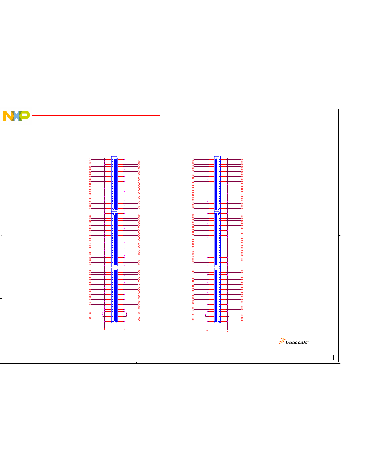
5
5
4
4
3
3
2
2
1
1
D D
C C
B B
A A
Socket
Not routed through the connectors:
- Crystal signals
- Specific MCU power pins (Power supplies are however taken to daughtercard)
(GND)
(GND)
(GND)
(GND)
(GND)
(GND)
(GND)
(GND)
(GND)
(GND)
(GND)
(GND)
(GND)
(GND)
(GND)
(GND)
(GND)
(GND)(GND)
(GND)
(GND)
(GND)
(GND)
(GND)
(GND)
(GND)
(GND)
(GND)
(GND)
(GND)
(GND)
(GND)
(GND)
(GND)
(GND)
(GND)
(GND)
(GND)
(GND)
(GND)
(GND)
(GND)
(GND)
(GND)
(GND)
(GND)
(GND)
(GND)
(GND)
(GND)
(GND)
(GND)
(GND)
(GND)
(GND)
(GND)
(GND)
(GND)
(GND)
(GND)
(GND)
(GND)
(GND)
(GND)
(GND)
(GND)
(GND)
(GND)
(GND)
Daughter Card Connectors (Sockets)
Socket
Notes:
- there was no neat way to fit these connectors onto a B sized sheet so unfortunately the sheet size has been
increased to C so will need to be printed on larger paper.
- The MCU Clock circuitry (apart from external clock) is local to the daughtercard so not pinned out on the
connectors
- Power is supplied to the daughtercard via MCU specific jumpered supplies (left connector) or direct supplies
from the regulators (right connector)
(GND) (GND)
(GND)
(GND)
(GND)
(GND)
(GND)
(GND)
(GND)
(GND) (GND)
(GND)(GND)
(GND)
(GND)
(GND)
(GND)
(GND)
(GND)
(GND)
(GND)
(GND) (GND)
(GND)
(GND)
(GND)
(GND) (GND)
PM11 PC1
PH10 PE3
PH4 PH5
PL4
PE15
PL9
PL3
PH12
PG11
PG10
PL8
PORSTx
PH11
PE14
PG15
PC4
PQ1
PQ2
PQ6
PP13
PP12
PE2
PA6
PA5
PQ4
PQ5
PQ7 PI4
PP15 PP14
PL12 PL2
PL13PL6
PM0
PM10
PL7
PM8
PH3
PM6
PI11
PI12PD12
PD9PD13
PI15PD10
PB7
PB3
PH8
PH7
PP8
PH6
PP3
PE7
PK9
PC12
PK11
PP4
PC8 PK14
PK13 PK12
PC9
PP2 PL0
PK15
PC15 PP1
PP7
PC14
PP6 PJ4
PO12
PO7
PO10
PO4 PH14
PO9 PO13
PO1PG5
PH13PO14
PO0 PG4
PI7 PH15
PP0 PO15
PE10
PE1 PE0
PI6 PO6
PO5
PE11 PG2
PG3 PA2
PE9
PE8 PA1
MCU-RSTx
PG9 PN15
PA0 PO3
PG7 PG6
PG8 PC11
PC10 PO2
PB0
PB10
PN0
PN6
PN3
PA15
PN10
PA4
PJ13
PN9
PJ9
PB1 PK1
PK2 PF12
PK3
PK5
PF11
PF9
PA14
PN13
PN11
PJ11
PJ10
PK0
PL10
PE5
PG14
PM12
PQ0
PI5
PC5
PQ3
PE4
PC3
PC2
PA8
PH2-R
PG0-R
PF14
PA9
PA10
PA7
PG1
PF15
PE13
PA11
PE12
PL11 PL5
PH1-R
PH0-R
PA3
PG12-R
PG13-R
PI13
PM4
PL1
PM5
PM3
PM14
PM13
PB12
PF5
PI9
PD8
PJ3
PJ2
PB4
PM15
PF2
PD7
PJ5
PJ0
PD5
PB5
PJ1
PD1
PB11
PI10
PD0
PB6
PN1
PF6
PD4
PI14
PJ7
PD11
PJ6
PD6
PD2
PJ8
PD3
MLB_DAT
MLB_CP
MLB_CN
MLB_CLK
MLB_SIG
MLB_SN
MLB_SP
MCU_5V0_S
MCU_1V25_L
MCU_3V3_S
MCU_3V3_L
MCU_5V0_L
PO11
PO8
PA12
PF0
PF1
PN2
PN5
PA13
PN4
PJ14
PN7
PF10
PN8
PJ15
PC7
PN12
PJ12
PF8
PK7
PC6
PF13
PK4
PK6
PN14
PK8
DC_3V3_S
DC_5V0_L
DC_3V3_L
DC_5V0_SDC_5V0_SDC_5V0_S
DC_P12V
DC_1V25_L
PF3
PF7
PF4
PL15
PM2
PM1
PL14
PM7
PM9
MLB_DN
MLB_DP
PE6
PI3
PP10
PP5
PI1
PI2
PP9
PC13
PI0
PK10
PB2
PP11
EXT-CLK
PC0
PH9
GND GND
GND GND
PH7
13
PH6
13
PB3
7
PP8
16
PH8
14
PP3
16
PE7
14
PK9
16
PC12
11
PK11
16
PP4
16
PK14
16
PK12
16
PC9
8
PL0
16
PP1
16
PC14
11
PJ4
16
PH14
16
PO13
16
PO1
12,16
PH13
16
PG4
12,15,16
PH15
16
PO15
16
PE10
12
PE0
13
PO6
16
PG2
12,15,16
PA2
15,16
PE9
12
PA1
15,16
MCU-RSTx
5,6
PN15
16
PO3
16
PG6
16
PC11
7
PO2
16
PB0
7
PK1
12,16
PF12
16
PK3
12,16
PK5
16
PF11
15,16
PC1
6
PE3
11
PH5
16
PQ3
9
PC3
9
PE4
11
PL10
6
PE15
9
PORSTx
5
PE2
11
PL4
6
PG11
9
PQ1
9
PG10
9
PQ2
9
PL8
6
PQ6
9
PP13
9
PP12
9
PI4
9
PP14
9
PL2
6
PL5
6
PL13
6
PM0
6
PA10
10
PA9
10
PA8
10
PF14
10
PG0-R
10
PH2-R
10
PG12-R
10
PG13-R
10
PM10
6
PM4
12,16
PL1
16
PM5
16
PI13
13,16
PB12
16
PD9
16
PI12
13,16
PB7
16
PI15
12
MLB_CN
13
MLB_CP
13
PI14
12
PJ7
16
PD11
16
PJ6
16
PD6
12,16
PD2
15,16
PD3
15,16
PJ8
16
PB6
16
PD0
15,16
PI10
16
PD4
12,16
PF6
12
PN1
16
PC8
8
PK13
16
PP2
16
PK15
16
PC15
11
PP7
16
PP6
16
PO12
16
PO7
16
PO10
16
PO4
16
PO9
16
PG5
12,15,16
PO14
16
PO0
12,16
PI7
9
PP0
16
PE1
13
PI6
9
PO5
16
PE11
12
PG3
12,15,16
PE8
12
PG9
13
PA0
14
PG7
16
PG8
16
PC10
7
PB1
7
PK2
12,16
PF9
15,16
PA14
12,16
PN13
16
PN11
16
PJ11
16
PJ10
16
PK0
12,16
PJ9
16
PN9
16
PJ13
16
PA4
16
PN10
16
PA15
12,16
PN3
16
PN6
16
PN0
16
PB10
12
PM11
16
PH10
6
PH4
16
PE5
11
PM12
16
PI5
9
PQ0
9
PC5
11
PG14
9
PH12
9
PC4
11
PL9
6
PC2
9
PA6
13
PL3
6
PH11
9
PA5
12
PE14
9
PQ4
9
PG15
9
PQ5
9
PQ7
9
PP15
9
PL12
6
PL11
6
PL6
6
PL7
6
PE12
10
PA11
10
PA7
10
PE13
10
PF15
10
PG1
10
PH1-R
10
PH0-R
10
PA3
10
PM8
6
PH3
16
PM3
12,16
PM6
16
PM13
16
PM14
16
PD13
12,13,16
PD12
16
PI11
10
PD10
16
MLB_DAT
13
MLB_SIG
13
MLB_CLK
13
MLB_SN
13
MLB_SP
13
PD7
12,16
PJ5
16
PJ0
12
PD5
12,16
PB5
16
PB11
16
PD1
15,16
PJ1
12
PD8
12,16
PI9
16
PF5
12
PB4
15
PJ2
12
PJ3
12
PF2
12
PM15
16
MCU_5V0_S
3
MCU_1V25_L
3
PO11
16
PO8
16
PN5
16
PA12
12,16
PN2
16
PF1
12
PF0
12
PN4
16
PA13
12,16
PN8
16
PF10
16
PN7
16
PJ14
16
PJ15
16
PC7
7
PN12
16
PJ12
16
PF8
16
PK7
16
PC6
7
PF13
16
PK4
12,16
PK6
16
PK8
16
PN14
16
DC_5V0_S
3
DC_P12V
3
DC_1V25_L
3
PF4
12
PF7
12
PF3
12
PL15
6
PM1
6
PM2
6
PL14
6
PM9
6
PM7
6
MLB_DN
13
MLB_DP
13
PE6
14
PI3
14
PP10
16
PP5
16
PI1
14
PI2
14
PP9
16
PC13
11
PI0
14
PK10
16
PB2
7
PP11
16
EXT-CLK
5
PC0
6
PH9
6
MCU_3V3_S 3
MCU_3V3_L 3
MCU_5V0_L 3
DC_3V3_S 3
DC_3V3_L 3
DC_5V0_L 3
Drawing Title:
Size Document Number Rev
Date: Sheet
of
Page Title:
Automotive Microcontroller
Applications
East Kilbride, Scotland
SCH-27897 PDF: SPF-27897 D1
MPC574xx Customer EVB Main Board
C
Friday, August 14, 2015
Daughter Card Connectors (Sockets)
416
Freescale General Business Use
Drawing Title:
Size Document Number Rev
Date: Sheet of
Page Title:
Automotive Microcontroller
Applications
East Kilbride, Scotland
SCH-27897 PDF: SPF-27897 D1
MPC574xx Customer EVB Main Board
C
Friday, August 14, 2015
Daughter Card Connectors (Sockets)
416
Freescale General Business Use
Drawing Title:
Size Document Number Rev
Date: Sheet of
Page Title:
Automotive Microcontroller
Applications
East Kilbride, Scotland
SCH-27897 PDF: SPF-27897 D1
MPC574xx Customer EVB Main Board
C
Friday, August 14, 2015
Daughter Card Connectors (Sockets)
416
Freescale General Business Use
P12
CON SKT 180
1
SH1 SH2
SH5 SH6
2
3 4
5 6
7 8
9 10
11 12
13 14
15 16
17 18
19 20
21 22
23 24
25 26
27 28
29 30
31 32
33 34
35 36
37 38
39 40
41 42
43 44
45 46
47 48
49 50
51 52
53 54
55 56
57 58
59 60
SH3 SH4
61 62
63 64
65 66
67 68
69 70
71 72
73 74
75 76
77 78
79 80
81 82
83 84
85 86
87 88
89 90
91 92
93 94
95 96
97 98
99 100
101 102
103 104
105 106
107 108
109 110
111 112
113 114
115 116
117 118
119 120
SH7 SH8
SH9 SH10
121 122
123 124
125 126
127 128
129 130
131 132
133 134
135 136
137 138
139 140
141 142
143 144
145 146
147 148
149 150
151 152
153 154
155 156
157 158
159 160
161 162
163 164
165 166
167 168
169 170
171 172
173 174
175 176
177 178
179 180
SH11 SH12
P13
CON SKT 180
1
SH1 SH2
SH5 SH6
2
3 4
5 6
7 8
9 10
11 12
13 14
15 16
17 18
19 20
21 22
23 24
25 26
27 28
29 30
31 32
33 34
35 36
37 38
39 40
41 42
43 44
45 46
47 48
49 50
51 52
53 54
55 56
57 58
59 60
SH3 SH4
61 62
63 64
65 66
67 68
69 70
71 72
73 74
75 76
77 78
79 80
81 82
83 84
85 86
87 88
89 90
91 92
93 94
95 96
97 98
99 100
101 102
103 104
105 106
107 108
109 110
111 112
113 114
115 116
117 118
119 120
SH7 SH8
SH9 SH10
121 122
123 124
125 126
127 128
129 130
131 132
133 134
135 136
137 138
139 140
141 142
143 144
145 146
147 148
149 150
151 152
153 154
155 156
157 158
159 160
161 162
163 164
165 166
167 168
169 170
171 172
173 174
175 176
177 178
179 180
SH11 SH12
Page 40
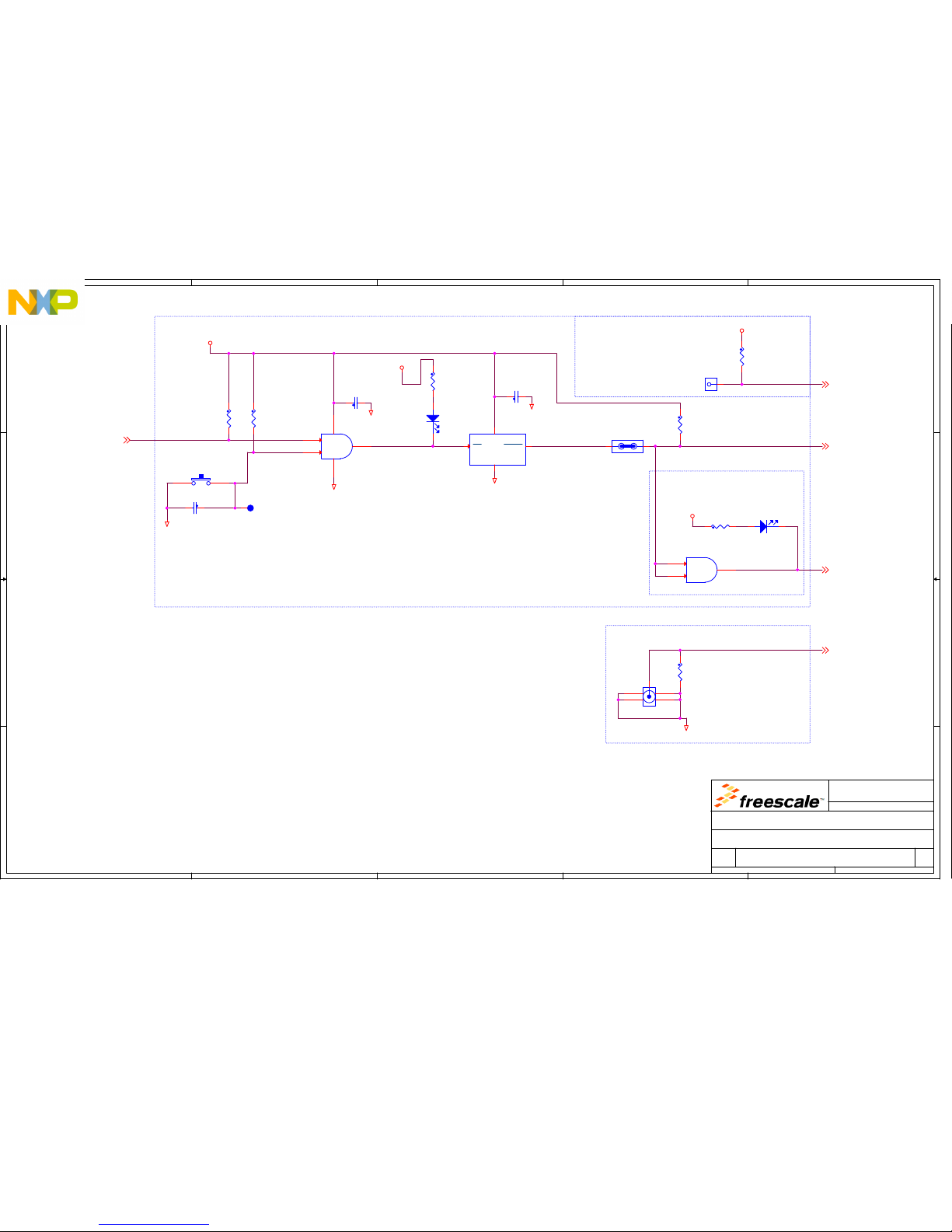
5
5
4
4
3
3
2
2
1
1
D D
C C
B B
A A
TARGET
RESET
LED
Reset Switch
(1.65 to 5.5v operation)
(MCU RESET)
Tri-State Buffered
RESET signal to
reset the MCU
Reset and External Clock In
Buffered RESET-out
Note:
The Reset pad on the MPC5748G is in the VDD_HV_A domain which can be run from either
3.3V or 5V (selected by the VDD_HV_A and PER_HVA jumpers)
To maintian brightness on the LED's irrespective of the voltage setting, the LED's are
powered from constant 3.3V, grounded via the reset line.
Bi Directional reset
line to/from MCU
Active reset drive (high / low)
for any periperhals that need to
be reset when MCU is in reset
Reset from
Debugger
Reset Input / Output
PORST
Connect an external LVI to pad
when supplying external 1.25V so
that PORST is asserted until
exterbal 1.25V supply is at
threshold and stable
(2.5 to 5v operation)
SMA style
Connector
External Clock In (SMA)
(0603
50V)
(0603
50V)
(0603
50V)
Reset is in the
VDD_HVA domain.
MCU-RSTx
JTAG-RSTx
RST-SWITCHx
RST-OUTx
RST-INxSYSTEM-RSTx
PORSTx
EXT-CLK
GND
GND
GND
3V3_SR
GND
GND
PER_HVA
3V3_SR
PER_HVA
GND
JTAG-RSTx
6
MCU-RSTx
4,6
RST-OUTx
10,12
PORSTx
4
EXT-CLK
4
Drawing Title:
Size Document Number Rev
Date: Sheet
of
Page Title:
Automotive Microcontroller
Applications
East Kilbride, Scotland
SCH-27897 PDF: SPF-27897 D1
MPC574xx Customer EVB Main Board
B
Friday, August 14, 2015
Reset Circuitry & External Clock In
516
Freescale General Business Use
Drawing Title:
Size Document Number Rev
Date: Sheet of
Page Title:
Automotive Microcontroller
Applications
East Kilbride, Scotland
SCH-27897 PDF: SPF-27897 D1
MPC574xx Customer EVB Main Board
B
Friday, August 14, 2015
Reset Circuitry & External Clock In
516
Freescale General Business Use
Drawing Title:
Size Document Number Rev
Date: Sheet of
Page Title:
Automotive Microcontroller
Applications
East Kilbride, Scotland
SCH-27897 PDF: SPF-27897 D1
MPC574xx Customer EVB Main Board
B
Friday, August 14, 2015
Reset Circuitry & External Clock In
516
Freescale General Business Use
R24
10.0K
J9
1 2
R214 270
R31
10.0K
SW1 B3WN-6002
1 2
C3
0.1UF
VCC
GND
U4A
SN74LVC2G08DCT
1
2
7
84
R4
10.0K
P7
CON 1 SMA
1
2
4 3
5
R217
270
TPV5
U4B
SN74LVC2G08DCT
5
6
3
C220
0.1UF
U3
ADM6315-26D2ARTZR7
GND
1
RESET
2
MR
3
VCC
4
R216
100
C224
0.1UF
R16
10.0K
DS1
YELLOW LED
AC
TPH1
1
D1
LED RED
A C
Page 41
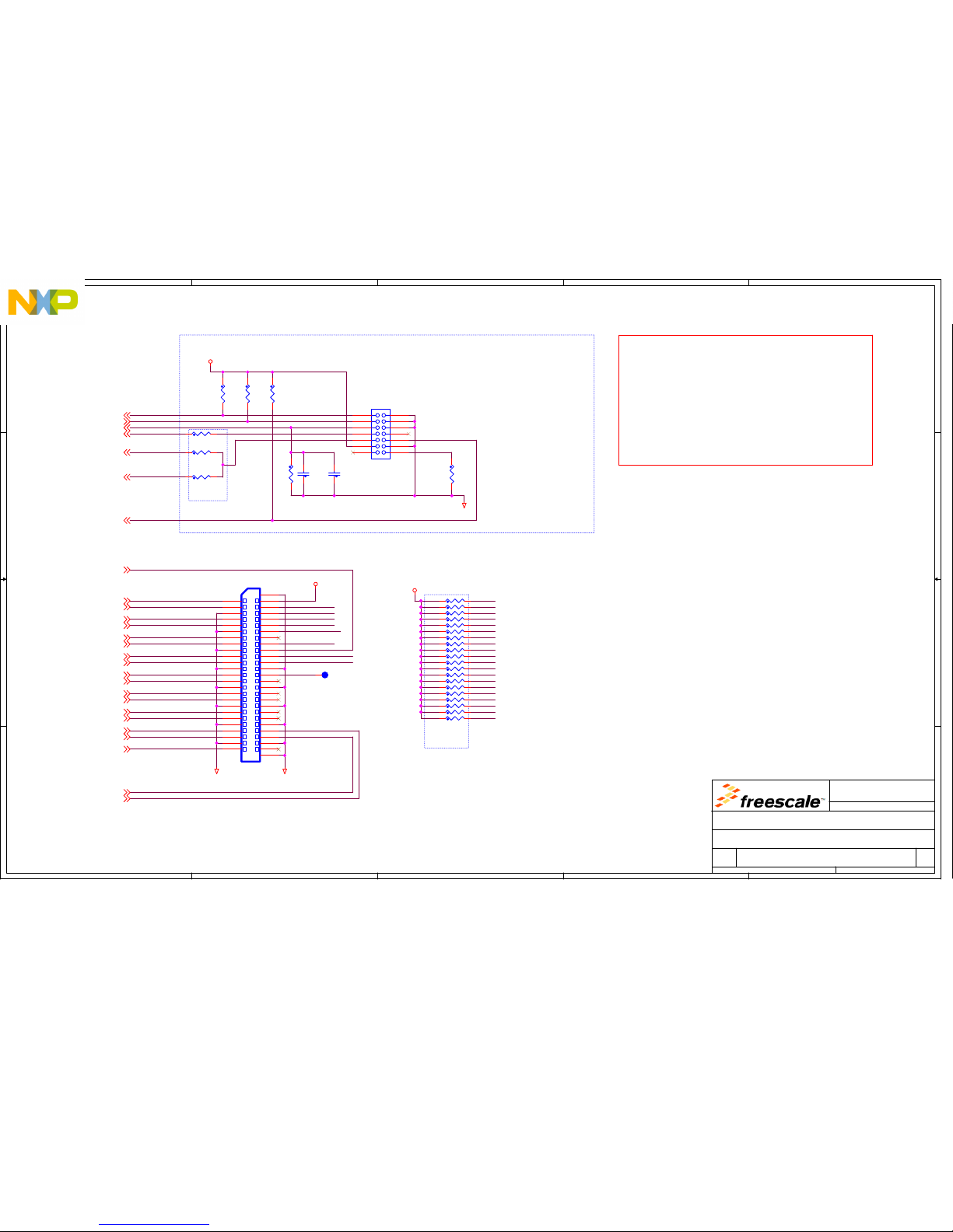
5
5
4
4
3
3
2
2
1
1
D D
C C
B B
A A
Debug Connectors (JTAG and NEXUS)
JTAG Standard 14-pin Connector
(RDY)
Place One CAP
next to each
connector
ONCE Connector
(N/C)
(TMS)
(JCOMP)
(GND)
(GND)
(GND)
(GND)
(TDI)
(TDO)
(TCLK)
(EVTI)
(RESET)
(VREF)
TDI
TDO
TCLK
(All JTAG reset pullups are on Reset Page)
(MSEO_0)
(MSEO_1)
(MDO4)
(GND)
(GND)
(GND)
(GND)
(TMS)
(TDI)
(TDO)
(GND)
(GND)
(GND)
(GND)
(JCOMP)
(RDY)
(EVTI)
(EVTO)
(GND)
(GND)
(MDO0)
(RST OUT)
(RESET)
(GND)
(GND)
(GND)
(GND)
(MDO1)
(MDO2)
(MDO3)
(MCKO)
(N/C)
(MDO5)
(MDO6)
(MDO7)
(MDO8)
(MDO9)
(MDO10)
(MDO14)
(ARBREQ)
(ARBGRT)
(MDO15)
(MDO13)
(MDO12)
(MDO11)
(GND)
(VREF)
(TCK)
(CLKOUT)
(TD/WT)
(DAI1)
(DAI2)
Nexus
(buffered
reset TO MCU)
(bidirectional
MCU reset)
Note on EVTI:
EVTI is an optional
signal. Although it is
supported on the JTAG
connector, tools vendors
do not normally use EVTI
on non trace hardware.
EVTI is powered from
VDD_HV_B whereas the
rest of the JTAG signals
are from VDD_HV_A. In
order to use EVTI on the
JTAG, connector,
VDD_HV_A and HV_B should
be set to the same
voltage. Rather than
impose this limitation
for all customers, a
zero ohm link has been
added to allow EVTI to
be enabled on the JTAG
connector if required.
Optional
Config
EVTI
TMS
NEXUS 50-pin Connector
Neus
Specific
Pullups all
10K 0603
All of the signals used for JTAG (with the
exception of EVTI, see note) are powered from
the VDD_HV_A domain. All of the additional
signals used for Nexus are powered from
VDD_HV_B.
If you are using Nexus, you need to ensure that
the VDD_HV_A and VDD_HV_B domains are at the
same voltage as well as ensuring that the
peripheral supplies PER_HVA and PER_HVB match
VDD_HV_A / B. See the MCU power page for
configuration jumpers.
Voltage Domains:
EVTI
JCOMP
PH10
PC0
PC1
PH10
PH9
DBUG-RSTx
PL9
PL11
PL2
PL3
PL4
PL5
PL10
PL6
PL7
PL13
PL14
PL15
PM0
PM1
PM2
PM7
PM10
PH9
PH10
PC0
PC1
JCOMP
PL8
PL12
DBUG-RSTx
PM8
PM9
MCU-RSTx
JTAG-RSTx
MCU-RSTx
PL8
PM9
PM8
PL12
PL9
PL11
PL2
PL3
PL4
PL5
PL10
PL6
PL7
PL13
PL14
PL15
PM0
PM1
PM2
PL12
PM7
PM10
PM9
PM8
GND
GND GND
PER_HVA
PER_HVB
PER_HVB
PH9
4
PC0
4
PC1
4
JTAG-RSTx
5
MCU-RSTx
4,5
PL8
4
PH10
4
PL12
4
PL7
4
PL9
4
PL11
4
PL2
4
PL3
4
PL4
4
PL5
4
PL10
4
PL6
4
PL13
4
PL14
4
PL15
4
PM0
4
PM1
4
PM2
4
PM7
4
PM10
4
PM9
4
PM8
4
Drawing Title:
Size Document Number Rev
Date: Sheet
of
Page Title:
Automotive Microcontroller
Applications
East Kilbride, Scotland
SCH-27897 PDF: SPF-27897 D1
MPC574xx Customer EVB Main Board
B
Friday, August 14, 2015
Debug Connectors (JTAG & Nexus)
616
Freescale General Business Use
Drawing Title:
Size Document Number Rev
Date: Sheet of
Page Title:
Automotive Microcontroller
Applications
East Kilbride, Scotland
SCH-27897 PDF: SPF-27897 D1
MPC574xx Customer EVB Main Board
B
Friday, August 14, 2015
Debug Connectors (JTAG & Nexus)
616
Freescale General Business Use
Drawing Title:
Size Document Number Rev
Date: Sheet of
Page Title:
Automotive Microcontroller
Applications
East Kilbride, Scotland
SCH-27897 PDF: SPF-27897 D1
MPC574xx Customer EVB Main Board
B
Friday, August 14, 2015
Debug Connectors (JTAG & Nexus)
616
Freescale General Business Use
R228
R247
R227
R2 0
DNP
R232
TPV11
R231
R230
R1
10.0K
R15
10.0K
R236
R240
R226
R239
R235
P10
CON 2X25
1
3
5
7
9
11
13
15
17
19
21
23
25
27
29
31
33
35
37
39
41
43
45
47
49
2
4
6
8
10
12
14
16
18
20
22
24
26
28
30
32
34
36
38
40
42
44
46
48
50
S1
S2
R238
P8
CON_2X7
1 2
3 4
65
7 8
9 10
11 12
13 14
R30
10.0K
R243
R19 0 DNP
R41
10.0K
R242
R3 0
R246
C20
47PF
DNP
R241
R237
C17
47PF
DNP
R245
R225
R229
R44
10.0K
Page 42
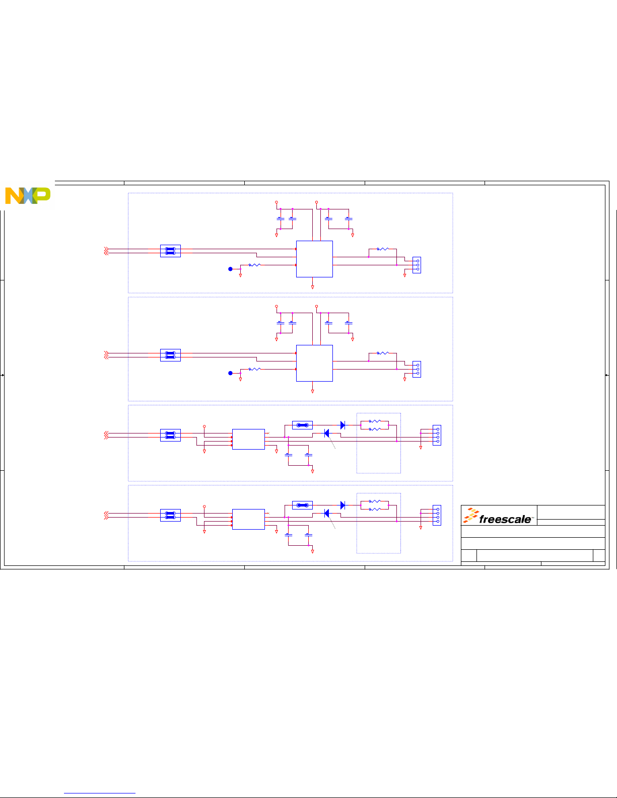
5
5
4
4
3
3
2
2
1
1
D D
C C
B B
A A
(Enable)
CAN & LIN Physical
EN = PER_HVA enables Transceiver and sets I/O for VDD_HV_A
(LIN0_TX)
(LIN0_RX)
(LIN1_RX)
(LIN1_TX)
VDD - 5.0V input supply for CAN transceiver (4.5 to 5.5V)
VI/O - determines the signal level on MCU TX and RX pins
and can range from 2.8 to 5.5V
STB - High for Standby mode, pulled low for normal mode.
CAN1 Physical Interface
(CAN0_RX)
(CAN0_TX)
(CAN1_RX)
(CAN1_TX)
(TXD_0)
LIN Molex
Connector
LIN1 Physical Interface
(0402
50V)
CAN0 Physical Interface
LIN Molex
Connector
Master Mode Pullup Enable
LIN0 Physical Interface
(0603
50V)
(0603
50V)
(0603
50V)
(0603
50V)
(0603
50V)
(LEF = 20K Baud)
Total current
through resistors
(LIN Bus at GND)
= 12mA (0.144W)
Each resistor spec
= 0.1W (0.2W total)
(Wake)
WAKE = GND ensures no spurious wakeups
(LEF = 20K Baud)
Total current
through resistors
(LIN Bus at GND)
= 12mA (0.144W)
Each resistor spec
= 0.1W (0.2W total)
(Wake)
(Enable)
EN = PER_HVA enables Transceiver and sets I/O for VDD_HV_A
(0402
50V)
Master Mode Pullup Enable
(0603
50V)
MC33662LEF LIN transceiver is newer version of 33661 offering:
- Full LIN compliance (33661 no longer compliant)
- Improved ESD protection on LIN pin up to 15KV
- Improved ESD on Wake and VSUP Pins
- Other EMC and performance improvements
See freescale.com for more details
WAKE = GND ensures no spurious wakeups
Battery
Reverse
polarity &
Pulse
Protection
Battery
Reverse
polarity &
Pulse
Protection
All CAN and LIN signals are
in power domain VDD_HV_A.
All interfaces will work at
3.3V or 5.0V (PER_HVA
jumper)
CAN termination resistor
footprint. Place on
underside of PCB
CAN termination resistor
footprint. Place on
underside of PCB
VDD - 5.0V input supply for CAN transceiver (4.5 to 5.5V)
VI/O - determines the signal level on MCU TX and RX pins
and can range from 2.8 to 5.5V
STB - High for Standby mode, pulled low for normal mode.
CAN0-CANLCAN0-S
PB0
LIN0-TX
PB1
PC10
PC11
PB3
PB2
PC7
PC6
LIN0-RX
LIN0-LIN
CAN1_TX
CAN0_TX
CAN0_RX
LIN1-TX
LIN1-RX
LIN1-LIN
LIN0-VSUP
LIN1-VSUP
CAN0-CANH
CAN1-S
CAN1_RX
CAN1-CANH
CAN1-CANL
PER_HVA
GND
GND
GNDGND
GND
GND
GNDGND
GND
GND
GNDGND
PER_HVA
GNDGND
GND
GND
PER_HVA
5V0_SR
GND GND
PER_HVA
5V0_SR
PB34
PB2
4
PC74
PC6
4
PC114
PB14
PB0
4
PC10
4
Drawing Title:
Size Document Number Rev
Date: Sheet
of
Page Title:
Automotive Microcontroller
Applications
East Kilbride, Scotland
SCH-27897 PDF: SPF-27897 D1
MPC574xx Customer EVB Main Board
B
Friday, August 14, 2015
CAN and LIN
716
Freescale General Business Use
Drawing Title:
Size Document Number Rev
Date: Sheet of
Page Title:
Automotive Microcontroller
Applications
East Kilbride, Scotland
SCH-27897 PDF: SPF-27897 D1
MPC574xx Customer EVB Main Board
B
Friday, August 14, 2015
CAN and LIN
716
Freescale General Business Use
Drawing Title:
Size Document Number Rev
Date: Sheet of
Page Title:
Automotive Microcontroller
Applications
East Kilbride, Scotland
SCH-27897 PDF: SPF-27897 D1
MPC574xx Customer EVB Main Board
B
Friday, August 14, 2015
CAN and LIN
716
Freescale General Business Use
R306 120
DNP
C256
0.1UF
D3 GF1A
AC
U12
MC33901WEF
GND
2
TXD
1
RXD
4
STB
8
CANH
7
CANL
6
VDD
3
VIO
5
R59 4.70K
C255
0.1UF
D201
GF1A
A C
D200 GF1A
A C
R25 2.0K
R249 2.0K
P14
HDR_1X3
1
2
3
C248
0.1UF
R221 2.0K
C257
0.1UF
P9
CON PLUG 4
1
2
3
4
C234
1000pF
C271
1uF
J12
1 2
3 4
J10
1 2
3 4
U10
MC33662LEF
RXD
1
EN
2
WAKE
3
TXD4GND
5
LIN
6
VSUP
7
INH
8
R58 4.70K
J15
1 2
3 4
U6
MC33662LEF
RXD
1
EN
2
WAKE
3
TXD4GND
5
LIN
6
VSUP
7
INH
8
C249
1000pF
C231
0.1UF
J13
1 2
C254
0.1UF
TPV15
C272
1uF
P15
HDR_1X3
1
2
3
D2 GF1A
AC
U11
MC33901WEF
GND
2
TXD
1
RXD
4
STB
8
CANH
7
CANL
6
VDD
3
VIO
5
J14
1 2
3 4
P11
CON PLUG 4
1
2
3
4
J11
1 2
R248 2.0K
TPV16
R307 120
DNP
C273
1uF
C270
1uF
Page 43
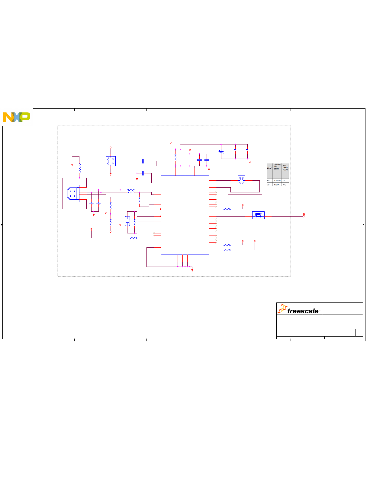
5
5
4
4
3
3
2
2
1
1
D D
C C
B B
A A
FTDI USB <-> Serial Interface
- Self Powered mode. No power is taken from USB
- Device efaults to Dual serial (RS232) mode ie RS232 on both A and B
- Configurable I/O voltage on CHA / CHB via VDDIOA/B
Send Immediate / Wakeup
Disabled for CHB
Send Immediate / Wakeup
Disabled for CHA
Disable Receiver when
in USB suspend mode
USB RS232 (serial) Interface
(MCU_LIN2RX)
(MCU_LIN2TX)
(0603
50V)
(0603
50V)
(0603
50V)
(0603
50V)
(0603
50V)
FTDI Pin 40 (TXD)
is Output from
FTDI Device,
connect to MCU RXD
FTDI Pin 39 (RXD)
is Input to FTDI
device, connect to
MCU TXD
All Signals are in
power domain
VDD_HV_A.
FTDI interface will
work at 3.3V or 5.0V
(PER_HVA jumper)
USB_N
BUS0
BUS1
BUS2
BUS3
BUS4
BUS5
CLK_XTIN_6M
CLK_XTOUT_6M
USB_RN
USB_P USB_RP
FTDI_TXD
FTDI_RXD
PC8
PC9
5V0_SR
GND
GND
GND
GND
5V0_SR
GND
GND
5V0_SR
GND
GND
5V0_SR
GND
GND
PER_HVA
PER_HVA
PER_HVA
PC9
4
PC8
4
Drawing Title:
Size Document Number Rev
Date: Sheet
of
Page Title:
Automotive Microcontroller
Applications
East Kilbride, Scotland
SCH-27897 PDF: SPF-27897 D1
MPC574xx Customer EVB Main Board
B
Friday, August 14, 2015
USB RS232 Interface
816
Freescale General Business Use
Drawing Title:
Size Document Number Rev
Date: Sheet of
Page Title:
Automotive Microcontroller
Applications
East Kilbride, Scotland
SCH-27897 PDF: SPF-27897 D1
MPC574xx Customer EVB Main Board
B
Friday, August 14, 2015
USB RS232 Interface
816
Freescale General Business Use
Drawing Title:
Size Document Number Rev
Date: Sheet of
Page Title:
Automotive Microcontroller
Applications
East Kilbride, Scotland
SCH-27897 PDF: SPF-27897 D1
MPC574xx Customer EVB Main Board
B
Friday, August 14, 2015
USB RS232 Interface
816
Freescale General Business Use
C261
0.033UF
R255
10.0K
L201
470OHM
DNP
12
C260
0.1UF
C259
0.1UF
R252
10.0K
R66 1.0M
X1
6 MHZ
13
2
C263
0.1UF
P18
HDR 2X3
DNP
1 2
3 4
65
1
2
34
+D
-D
G
V
P17
USB_TYPE_B
1
2
3
4
S1
S2
+
C22
10UF
R25310.0K
R69 27
C24
47PF
DNP
C23
47PF
DNP
R250 10.0K
DNP
R251
470
R68
27
C258
0.1UF
R256
4.70K
D2
D3D4
D1
D4
BGX50A
1
2
3
4
R254 10.0K
J16
1 2
3 4
C262
0.1UF
R67
1.5K
U13
FT2232D
ADBUS0
24
ADBUS1
23
ADBUS2
22
ADBUS3
21
ADBUS4
20
ADBUS5
19
ADBUS6
17
ADBUS7
16
ACBUS0
15
ACBUS1
13
ACBUS2
12
ACBUS3
11
SI/WUA
10
BCBUS0
30
BCBUS1
29
BCBUS2
28
BCBUS3
27
SI/WUB
26
PWREN#
41
3V3OUT
6
USBDM
8
USBDP
7
RSTOUT#
5
RESET#
4
XTIN
43
XTOUT
44
EECS
48
EESK
1
EEDATA
2
TEST
47
AVCC
46
VCC13VCC2
42
VCCIOA14VCCIOB
31
GND19GND218GND325GND4
34
AGND
45
BDBUS0
40
BDBUS1
39
BDBUS2
38
BDBUS3
37
BDBUS4
36
BDBUS5
35
BDBUS6
33
BDBUS7
32
Page 44
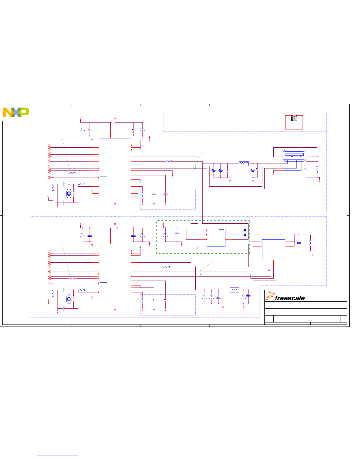
5
5
4
4
3
3
2
2
1
1
D D
C C
B B
A A
Adobe Acrobat
Document
USB (Type A Host and Type AB OTG)
(10V
0603
low
ESR)
(0603
50V)
Layout Note:
Place caps &
resistor as
close to
device as
possible
USB Power Switch
(USB1_DO)
(USB1_D1)
(USB1_D2)
(USB1_D3)
(USB1_D4)
(USB1_D5)
(USB1_D6)
(USB1_D7)
(USB1_DIR)
(USB1_STP)
(USB1_NXT)
(USB0_DO)
(USB0_D1)
(USB0_D2)
(USB0_D3)
(USB0_D4)
(USB0_D5)
(USB0_D6)
(USB0_D7)
(USB0_DIR)
(USB0_STP)
(USB0_NXT)
(Only available on BGA packages)
(Available on all packages)
(USB1_RST Active Low)
(0603
50V)
(1210
2KV)
USB Host, Type A
(35V
TANT)
(35V
TANT)
(1210
2KV)
(50V
0402)
(16V
TANT)
(35V
TANT)
(0402
50v)
(16V
TANT)
(Select 60MHz CLKOUT
with 24MHz XTAL)
(16V
TANT)
(35V
TANT)
(0402
50v)
(16V
TANT)
(50V
0402)
USB OTG Micro AB
(1/10W 0603)
(0603
50V)
(35V
TANT)
(0603
50V)
(35V
TANT)
(0603
50V)
(35V
TANT)
(10V
0603
low
ESR)
(10V
0603
low
ESR)
(1/10W 0603)
(10V
0603
low
ESR)
(USB0_RST Active Low)
(ID=GND for HOST mode)
(20K for HOST)
(Layout Note: Place Series
Termination resistor close
to USB IC)
(Layout Note: Route DP and DM with
90 Ohm Differential Pair. Keep
tracks as short as possible)
(Layout Note: Route DP and DM with
90 Ohm Differential Pair. Keep
tracks as short as possible)
General Layout Note. Recommendation is to keep all
tracks between MCU and USB PHI less than 3" See
additional SMSC Layout guidelines PDF to the right
(Layout Note: Place Series
Termination resistor close
to USB IC)
(1K for OTG)
Layout Note:
Place caps &
resistor as
close to
device as
possible
Crystals are
FOXSDLF/240F-20
(20pF Load
Capacitance)
Crystals are
FOXSDLF/240F-20
(20pF Load
Capacitance)
USB Signals
are in
power
domain
VDD_HV_A
The USB
interface
only supports
3.3V
operation.
All I/O
signals must
be 3.3V. If
VDD_HVA is
set to 5V,
USB MCU pads
must be left
as tri-state
with no
pullups.
USB_A_VDD1.8
USB_A_VDD3.3
PP15
PP14
PP13
PP12
PQ7
PQ6
PQ5
PQ4
PQ2
PQ0
PQ3
PQ1
USB_A_EN
USB_A_PWR
PI6
USB_B_EN
USB_B_EN
USB_B_DP
PI7
USB_A_EN
USB_A_VBUS
USB_A_DM
USB_A_DP
USB_B_PWR
USB_B_VBUS
USB_B_DP
USB_B_DM
USB_B_DM
USB_B_ID USB_B_ID
USB_A_DM
USB_A_5V
USB_B_5V
USB_A_DP
PG14
PG15
PE14
PE15
PG10
PG11
PH11
PH12
PC3
PI4
PI5
PC2
USB_B_VDD1.8
USB_B_VDD3.3
FLG_A
FLG_B
A_XO
A_XI
B_XI
B_XO
USB1_CLK
USB0_CLK
3V3_SR
GND
5V0_SR
GND
5V0_SR
GND
GND
GND
GND GNDGND
GND
GND
GND GNDGND
GND
GND
GND
GND
GND
GND
3V3_SR
GND
5V0_SR
3V3_SR
GNDGNDGND
3V3_SR
3V3_SR
3V3_SR
GND
GND
PI6
4
PG15
4
PE14
4
PE15
4
PG10
4
PG11
4
PH11
4
PH12
4
PI44
PI54
PC24
PC34
PG14
4
PP14
4
PP13
4
PP12
4
PQ7
4
PQ6
4
PQ5
4
PQ4
4
PP15
4
PQ04
PQ34
PQ14
PQ24
PI7
4
Drawing Title:
Size Document Number Rev
Date: Sheet
of
Page Title:
Automotive Microcontroller
Applications
East Kilbride, Scotland
SCH-27897 PDF: SPF-27897 D1
MPC574xx Customer EVB Main Board
B
Friday, August 14, 2015
USB Type A / Type AB
916
Freescale General Business Use
Drawing Title:
Size Document Number Rev
Date: Sheet of
Page Title:
Automotive Microcontroller
Applications
East Kilbride, Scotland
SCH-27897 PDF: SPF-27897 D1
MPC574xx Customer EVB Main Board
B
Friday, August 14, 2015
USB Type A / Type AB
916
Freescale General Business Use
Drawing Title:
Size Document Number Rev
Date: Sheet of
Page Title:
Automotive Microcontroller
Applications
East Kilbride, Scotland
SCH-27897 PDF: SPF-27897 D1
MPC574xx Customer EVB Main Board
B
Friday, August 14, 2015
USB Type A / Type AB
916
Freescale General Business Use
Y3
24MHZ
1 2
C16
33PF
R33
10
R39
8.06K
1%
+
C239
10UF
R36 20K
+
C5
1.0UF
C214
1000pF
+
C230
10UF
+
C244
10UF
+
C212
100UF
C13
33PF
TPV12
L3 26OHM
1 2
C10
1000pF
C2
1000pf
Y4
24MHZ
1 2
R213
100
+
C205
10UF
C19
1uF
+
C245
10UF
+
C9
1.0UF
C14
33PF
R27
1.0M
VD-D+G
USB_TYPE_A_FEMALE
P5
S1
A1
A2
A3
A4
S2
U7
USB83340
CPEN
17
VBUS
22
ID
23
VBAT_5V
21
DP
18
DM
19
RESET
27
NXT
2
DIR
31
STP
29
CLKOUT
1
VDD3V3_20
20
VDD1V8_28
28
XO
25
REFCLK/XI
26
VDD1V8_30
30
RBIAS
24
VDDIO
32
DATA7
13
DATA6
10
DATA5
9
DATA4
7
DATA3
6
DATA2
5
DATA1
4
DATA0
3
PAD_GND
33
SPK_L
15
SPK_R
16
REFSEL0
8
REFSEL1
11
REFSEL2
14
NC
12
C242
0.1UF
C243
0.1UF
L4 26OHM
1 2
R32
10
R202
100
C4
1000pF
U8
USB83340
CPEN
17
VBUS
22
ID
23
VBAT_5V
21
DP
18
DM
19
RESET
27
NXT
2
DIR
31
STP
29
CLKOUT
1
VDD3V3_20
20
VDD1V8_28
28
XO
25
REFCLK/XI
26
VDD1V8_30
30
RBIAS
24
VDDIO
32
DATA7
13
DATA6
10
DATA5
9
DATA4
7
DATA3
6
DATA2
5
DATA1
4
DATA0
3
PAD_GND
33
SPK_L
15
SPK_R
16
REFSEL0
8
REFSEL1
11
REFSEL2
14
NC
12
U9
MIC2026-1YM
ENA1FLGA
2
FLGB
3
ENB
4
OUTB
5
GND
6
IN7OUTA
8
R46
10.0K
C18
1uF
+
C216
10UF
P1
USB AB 5
VBUS1D-2D+3ID4GND
5
SHELL1
6
SHELL27SHELL3
8
SHELL4
9
R26
1.0M
+
C247
10UF
R37 1.0K
C238
1uF
R47
10.0K
R48
30
C246
0.1UF
C15
33PF
R49
30
TPV13
C206
1000pf
C237
1uF
R38
8.06K
1%
C1
1000pF
C236
0.1UF
C235
0.1UF
+
C8
100UF
Page 45
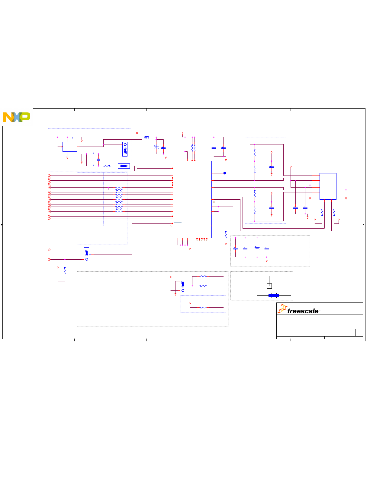
5
5
4
4
3
3
2
2
1
1
D D
C C
B B
A A
Ethernet
Place Caps close
to connector
Series Termination Resistors:
50 Ohms as per TI spec. Place
resistors as close to driving
source as possible. Termination
recommended for ALL MII signals
MCU Output
Resistors Next
to MCU on
daughtercard
PHI Output
Place Next to
PHI
- Auto Negotiation Enable (All speeds / duplex supported)
(AN_EN, AN0 and AN1 all Internal PullUP)
- Operating Mode (MII or RMII)
(SNI_Mode Internal PullDown, MII_Mode control via jumper)
- LED Configuraiton (Mode1)
(LED_CFG Internal PullUp)
- MDIX Enable (Auto MDIX Enabled)
(MDIX_EN Internal PullUP)
- Physical Address (set to 0b00001)
(PHYAD[0] Internal PullUp, PHYAD[1..4] Internal PullDown)
(MII_MODE)
Posn 1-2 for MII (default)
Posn 2-3 for RMII
Pulse J1011F21PNL
(Includes built in
transformer)
Layout Note - Place Caps
and Resistors close to PHI
(RMII Clock)
(RMII)
(RMII)
(RMII)
(RMII)
(RMII)
(+MII)
(+MII)
(+MII)
(+MII)
(RMII)
(RMII)
(RMII)
(RMII)
(+MII)
(+MII)
(RMII)
(+MII)
(RMII)
(RMII)
(MII Clock)
(TANT)
Layout Note:
Place 0.1uF cap close
to each pin. 10uF
TANT as close to pin
23 as possible
PFBOUTPFBIN2PFBIN1
50MHz Osc for RMII and 25MHz XTAL for MII
(TANT)
Reset Control:
- Reset from MCU Reset Out (will reset with MCU)
- Reset from GPIO. Allows MCU to reset PHY as well as hold PHY in reset
while reset config data can be driven onto pins to change mode etc.
Boot Configuration (using PHY internal Pulls)
MDIO Pullup
Layout Note:
MII Mode resistor (MII / RMII mode) and the MDIP ullup resistor should be placed as close as
possible to the PF15 / PF14 tracks to reduce the effect of a stub on the transmission line.
(TXD3)
(TXD2)
(TXD1)
(TXD0)
(TXEN)
(MDC)
(Termination on DC)
(Termination on DC)
(Termination on DC)
(Termination on DC)
(Termination on DC)
(Termination on DC)
(0603
50V)
(0603
50V)
(0603
50V)
(0603
50V)
(0603
50V)
(0603
50V)
(0603
50V)
(0603
50V)
(0603
50V)
(0603
50V)
(0603
50V)
(MDIO)
All Ethernet Signals
are in power domain
VDD_HV_B
The Ethernet
interface only
supports 3.3V
operation. All I/O
signals must be 3.3V.
If VDD_HVA is set to
5V, Ethernet MCU pads
must be left as
tri-state with no
pullups.
(50MHz OSC
Power)
** See Layout Note
(bottom right)
** Layout Note - Place
resistors as shown
with shared pad on PG1
side of resistors
TXCLKPG1
PHY_50MHz
For RMII mode,
remove resistor
between PG1 and
TXCLK and place
between PG1 and
PHY_50MHz
TDN
TDP
RDN
LED_Y
LED_G
RBIAS
PA3
PE12
PA10
PA11
PF15
PA9
PA8
PA7
PE13
PG1
PF15
RDP
RST-OUTxRST-OUTx
X2
PHY_50MHz
PHY_25MHz
TXCLK
PH2-R
PH1-R
PH0-R
RXDV
PFBOUT
RXER
RXD1
RXD0
CRS
PG13-R
PG12-R
RXD3
RXD2
COL
RXCLK
PG0-R
RMII_50MHZ
PFBOUT
PF14
PF14
PI11
CLKIN_X1
RMII_50MHZ
GND
3V3_SR
GNDGND
3V3_SR3V3_SR
GND
GND
GND
3V3_SR
GND
GND
3V3_SR
3V3_SR
GND
GND
3V3_SR
GND
GND
GND
3V3_SR
GND
3V3_SR
3V3_SR
PE134
RST-OUTx
5,12
PG0-R
4
PG14
PA74
PA84
PA94
PF154
PA114
PA104
PE124
PA34
PF14
4
PI11
4
PG13-R
4
PG12-R
4
PH0-R
4
PH1-R
4
PH2-R
4
Drawing Title:
Size Document Number Rev
Date: Sheet
of
Page Title:
Automotive Microcontroller
Applications
East Kilbride, Scotland
SCH-27897 PDF: SPF-27897 D1
MPC574xx Customer EVB Main Board
B
Friday, August 14, 2015
Ethernet
10 16
Freescale General Business Use
Drawing Title:
Size Document Number Rev
Date: Sheet of
Page Title:
Automotive Microcontroller
Applications
East Kilbride, Scotland
SCH-27897 PDF: SPF-27897 D1
MPC574xx Customer EVB Main Board
B
Friday, August 14, 2015
Ethernet
10 16
Freescale General Business Use
Drawing Title:
Size Document Number Rev
Date: Sheet of
Page Title:
Automotive Microcontroller
Applications
East Kilbride, Scotland
SCH-27897 PDF: SPF-27897 D1
MPC574xx Customer EVB Main Board
B
Friday, August 14, 2015
Ethernet
10 16
Freescale General Business Use
R21
2.2K
5%
R233
49.9
1%
R220 1.5K
J5
1
2
3
J7
1
2
3
dp83848c
U5 10/100 single phy
RXCLK
38
RSVDPU221RSVDPU1
20
RSVD512RSVD411RSVD310RSVD29RSVD1
8
RDN
13
RDP
14
LEDACTCOL_ANEN
28
IOVDD33_248IOVDD33_1
32
IOGND_247IOGND_135DGND
36
AVDD33
22
AGND_215AGND_1
19
TXD2
5
TXCLK
1
LEDLINK_AN0
26
RXER_MDIXEN
41
MDC
31
RESET
29
PWRDN_INT
7
MDIO
30
CRS_LEDCFG
40
RXD3_PHYAD3
46
RXD2_PHYAD2
45
RXD1_PHYAD1
44
RXD0_PHYAD1
43
RXDV_MIIMODE
39
TXEN
2
TXD0
3
LEDSPEED_AN1
27
PFBIN2
37
TXD3_SNIMODE
6
TXD1
4
RBIAS
24
COL_PHYAD0
42
PFBIN1
18
PFBOUT
23
X2
33
X1
34
TDN
16
TDP
17
25MHZ_OUT
25
C200
0.1UF
C228
0.1UF
J6
1 2
R5 50
C225
0.1UF
Y2
25MHZ
21
R34 50
C227
0.1UF
R28 50
C233
0.1UF
L200
120OHM
21
R218
10.0K
+
C241
10UF
R42 50
R222
270
C232
0.1UF
R43 50
C223
0.1UF
C211
33PF
C229
0.1UF
R80 50 DNP
C11
0.1UF
R224
49.9
1%
R219
2.2K 5%
R17 50
R244
49.9
1%
R215
0
R223
270
CLK
OUT
VDD
GND
OE
50MHZ
Y1
42
31
+
C240
10UF
C210
33PF
J8
1
2
3
C6
0.1UF
R20 50
P6 RJ45-8
TD+
1
TD-
2
CT_3
3
GND_4
4
GND_5
5
CT_6
6
RD+
7
RD-
8
YA9YC10GC11GA
12
GND1
CG1
GND2
CG2
R35 50
C226
0.1UF
R18
4.87K
R29
2.2K
5%
R40 50
R234
49.9
1%
R45 50
R308 0
TPV10
Page 46
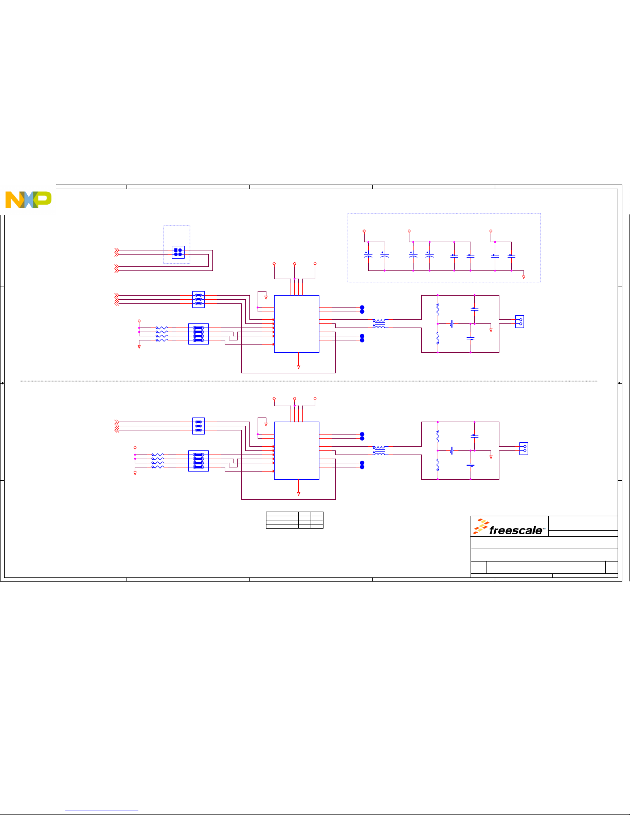
5
5
4
4
3
3
2
2
1
1
D D
C C
B B
A A
FlexRAY Physical Interface
FlexRAY
debug
connector
Decoupling Caps for BOTH IC's. Place next to power pins.
FlexRAY A
Normal
EN STBN
1
Sleep
Go to Sleep
Rec Only 011
1
MODE
00
0
VBAT VBUF VCC VIO
(FR_A_TX)
(FR_A_RX)
(FR_A_TX_EN)
(FR_B_TX)
(FR_B_TX_EN)
(FR_B_RX)
(FR_DBG0) (FR_DBG1)
(FR_DBG2) (FR_DBG3)
FlexRAY B
(0603
50V)
(0603
50V)
(0603
50V)
(0603
50V)
Crimped lead - 279-9522
Receptacle housing - 279-9156
Crimped lead - 279-9522
Receptacle housing - 279-9156
(0603)
(0603)
(0603)
(0603)
(50V 0805)
(50V 0805)
Bus voltage +/- 12V (VBAT = 12v)
Components spec'd for 12V operation
Bus voltage +/- 12V (VBAT = 12v)
Components spec'd for 12V operation
All Signals are in
power domain VDD_HV_A.
FlexRAY interface will
work at 3.3V or 5.0V
(PER_HVA jumper)
FRA-WAKE
FRA-INH1
PC5
FRA-JRXD
PE2
FRA-BGE
PE3
FRA-JTXD
FRA-JTXEN
FRA-BM FRA-DATA-B
FRA-STBN
FRA-BP
FRB-INH2
PE4
PC4
FRB-BGE
PE5
FRB-JTXD
FRB-JTXEN
FRB-JRXD
FRB-BM FRB-DATA-B
FRB-STBN
FRB-BP
FRB-EN
FRB-INH1
FRB-RXEN
FRB-DATA-A
FRB-ERRN
FRA-EN
FRB-WAKE
FRA-INH2
FRA-RXEN
FRA-DATA-A
FRA-ERRN
PC14
PC12
PC15
PC13
GND
GND
GND
GND
GND
PER_HVA
5V0_SR P12V
PER_HVA
5V0_SR P12V
GND
PER_HVA
P12V 5V0_SR
PER_HVA
GND
GND
GND
PER_HVA
PC12
4
PC14
4
PC15
4
PC13
4
PC5
4
PE2
4
PE34
PE4
4
PC4
4
PE54
Drawing Title:
Size Document Number Rev
Date: Sheet
of
Page Title:
Automotive Microcontroller
Applications
East Kilbride, Scotland
SCH-27897 PDF: SPF-27897 D1
MPC574xx Customer EVB Main Board
B
Friday, August 14, 2015
FlexRAY Physical Interface
11 16
Freescale General Business Use
Drawing Title:
Size Document Number Rev
Date: Sheet of
Page Title:
Automotive Microcontroller
Applications
East Kilbride, Scotland
SCH-27897 PDF: SPF-27897 D1
MPC574xx Customer EVB Main Board
B
Friday, August 14, 2015
FlexRAY Physical Interface
11 16
Freescale General Business Use
Drawing Title:
Size Document Number Rev
Date: Sheet of
Page Title:
Automotive Microcontroller
Applications
East Kilbride, Scotland
SCH-27897 PDF: SPF-27897 D1
MPC574xx Customer EVB Main Board
B
Friday, August 14, 2015
FlexRAY Physical Interface
11 16
Freescale General Business Use
C201
10PF
R200 10.0K
P4
DNP
1 2
3 4
J3
HDR 2X3
1 2
3 4
65
C218
0.1UF
R207
47.0
1%
TPV6
C215
0.1UF
TPV9
+
C209
10UF
U1
TJA1080TS/N
TRXD0
11
TRXD1
10
TXD
5
TXEN
6
BGE
8
STBN
9
EN
3
WAKE
15
INH2
1
INH1
2
BP
18
BM
17
RXD
7
ERRN
13
RXEN
12
VIO
4
VCC
19
VBUF
20
VBAT
14
GND
16
TPV3
R212 10.0K
R206 10.0K
TPV7
R209
47.0
1%
C213
0.1UF
R201 10.0K
R205 10.0K
+
C217
10UF
TPV4
C203
10PF
C219
0.1UF
C202
10PF
U2
TJA1080TS/N
TRXD0
11
TRXD1
10
TXD
5
TXEN
6
BGE
8
STBN
9
EN
3
WAKE
15
INH2
1
INH1
2
BP
18
BM
17
RXD
7
ERRN
13
RXEN
12
VIO
4
VCC
19
VBUF
20
VBAT
14
GND
16
TPV8
R203 10.0K
J1
1 2
3 4
5 6
7 8
R210
47.0
1%
C208
4700PF
L2
DLW43SH
21
4 3
L1
DLW43SH
21
4 3
C207
4700PF
R208
47.0
1%
P2
1
2
+
C221
10UF
TPV2
R211 10.0K
J2
1 2
3 4
5 6
7 8
+
C222
10UF
R204 10.0K
J4
HDR 2X3
1 2
3 4
65
C204
10PF
P3
1
2
TPV1
Page 47
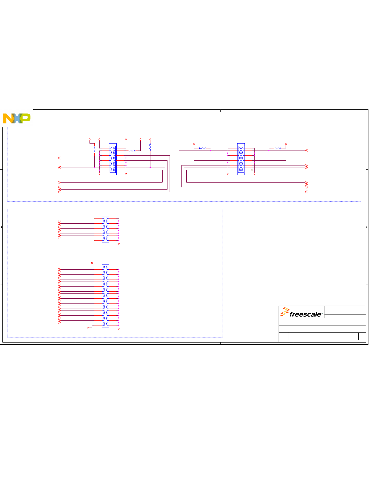
5
5
4
4
3
3
2
2
1
1
D D
C C
B B
A A
SAI Audio, AVB & TWRPI Connectors
(SAI0_DATA3)
(SAI0_DATA2)
(SAI0_DATA1)
(SAI0_DATA0)
(SAI0_BCLK)
(SAI0_SYNC)
(SAI0_MCLK)
(SAI1_DATA0)
(SAI1_BCLK)
(SAI1_SYNC)
(SAI1_MCLK)
(SAI2_DATA0)
(SAI2_BCLK)
(SAI2_SYNC)
(SAI2_MCLK)
(I2C_SCL2)
(I2C_SDA2)
(I2C_SDA3)
(I2C_SCL3)
(ENET0_TMR0)
Green - I2C Channels
Black - SAI Channels
Orange - ENET TMRx channels
(ENET1_TMR2)
(ENET0_TMR2)
(GPIO Control)
Differences to RevC
Pin 17 was PH5, now PD13** (PH5 now routed to GPIO Matrix)
Pin 27 was PH4, now PM4 (PH4 now routed to GPIO Matrix)
Pin 45 was PH3, now PM3 (PH3 now routed to GPIO Matrix)
** Note PD13 is also routed to MLB header via DNP link
Pins used on this header are also at GPIO Matrix
PA12 - DSPI0_SIN (Also shared with TWRPI)
PA13 - DSPI0_SOUT (Also shared with TWRPI)
PA14 - DSPI0_SCK (Also shared with TWRPI)
PA15 - DSPI0_SS0 (Also shared with TWRPI)
PG2 - DSPI3_SOUT (Also shared with User LED)
PG3 - DSPI3_SS3 (Also shared with User LED)
PG4 - DSPI3_SCLK (Also shared with User LED)
PG5 - DSPI3_SIN (Also shared with User LED)
(DSPI0_SIN)
(DSPI0_SOUT)
(DSPI0_SCK)
(DSPI0_SS0)
(DSPI3_SOUT)
(DSPI3_SS3)
(DSPI3_SCK)
(DSPI3_SIN)
I2C0_SCL
(DSPI0_SOUT)
(GPIO0/IRQ)
(GPIO2)
(GPIO4)
I2C0_SDA
(DSPI0_SIN)
(GPIO1)
(GPIO3)
General Purpose TWRPI
TWRPI-ADC1
TWRPI-ID0
TWRPI-ADC0
TWRPI-ADC2
TWRPI-ID1
(ADC1_P[8])
(ADC1_P[9])
(ADC1_P[10])
(ADC1_P[11])
(ADC1_P[12])
Note: Ports
PD[4..8] are
shared with the
GPIO Matrix
(EIRQ31)
Note: Ports
PK[0..5] are
shared with the
GPIO Matrix
(DSPI0_SCK)(DSPI0_SS0)
RESET
SAI Audio and AVB
PF2
PF3
PF4
PF5
PF1
PB10
PF0
PJ2
PJ3
PF7
PI14
PJ1
PJ0
PI15
PE11
PE10
PE9
PE8
PF6
PA5
PD13
PM4
PM3
PA12
PA13
PA14
PA15
PG2
PG3
PG4
PG5
PK0
PO0
PD6
PD5
PD4
PK4
PA14
RST-OUTx
PA15
PA13PA12
PK2
PK3
PD5
PD4
PD7
PD8
PO1
PK1
PO0
PK4
PK1
PK3
PD8
RST-OUTx
GND
3V3_SR
5V0_SR
GND
3V3_SR 3V3_SR
GND GND
5V0_SR 3V3_SR
GND GND
3V3_LR3V3_SR 3V3_SR
PF2
4
PF3
4
PF4
4
PF5
4
PF1
4
PB10
4
PF0
4
PE11
4
PJ3
4
PF7
4
PE9
4
PE8
4
PI14
4
PJ1
4
PJ0
4
PJ2
4
PE10
4
PI15
4
PF6
4
PA5
4
PD13
4,13,16
PM4
4,16
PM3
4,16
PA12
4,16
PA13
4,16
PA14
4,16
PA15
4,16
PG2
4,15,16
PG3
4,15,16
PG4
4,15,16
PG5
4,15,16
PD74,16
PD64,16
PD84,16
PD44,16
PD54,16
PO0
4,16
PO1
4,16
PK0
4,16
PK2
4,16
PK4
4,16
PK1
4,16
PK3
4,16
RST-OUTx
5,10
Drawing Title:
Size Document Number Rev
Date: Sheet
of
Page Title:
Automotive Microcontroller
Applications
East Kilbride, Scotland
SCH-27897 PDF: SPF-27897 D1
MPC574xx Customer EVB Main Board
B
Friday, August 14, 2015
SAI Audio, AVB & TWRPI Headers
12 16
Freescale General Business Use
Drawing Title:
Size Document Number Rev
Date: Sheet of
Page Title:
Automotive Microcontroller
Applications
East Kilbride, Scotland
SCH-27897 PDF: SPF-27897 D1
MPC574xx Customer EVB Main Board
B
Friday, August 14, 2015
SAI Audio, AVB & TWRPI Headers
12 16
Freescale General Business Use
Drawing Title:
Size Document Number Rev
Date: Sheet of
Page Title:
Automotive Microcontroller
Applications
East Kilbride, Scotland
SCH-27897 PDF: SPF-27897 D1
MPC574xx Customer EVB Main Board
B
Friday, August 14, 2015
SAI Audio, AVB & TWRPI Headers
12 16
Freescale General Business Use
R318 10.0KR315
10.0K
R316
10.0K
R317 10.0K
P24
HDR_2X25
1 2
3 4
65
7 8
9 10
11 12
13 14
15 16
17 18
19 20
21 22
23 24
25 26
27 28
29 30
31 32
33 34
35 36
37 38
39 40
41 42
43 44
45 46
47 48
49 50
P25
HDR_10X2
DNP
1 2
3 4
65
7 8
9 10
11 12
13 14
15 16
17 18
19 20
P27
CON_2X10
1 2
3 4
65
7 8
9 10
11 12
13 14
15 16
17 18
19 20
P26
CON_2X10
1 2
3 4
65
7 8
9 10
11 12
13 14
15 16
17 18
19 20
R314 0
Page 48
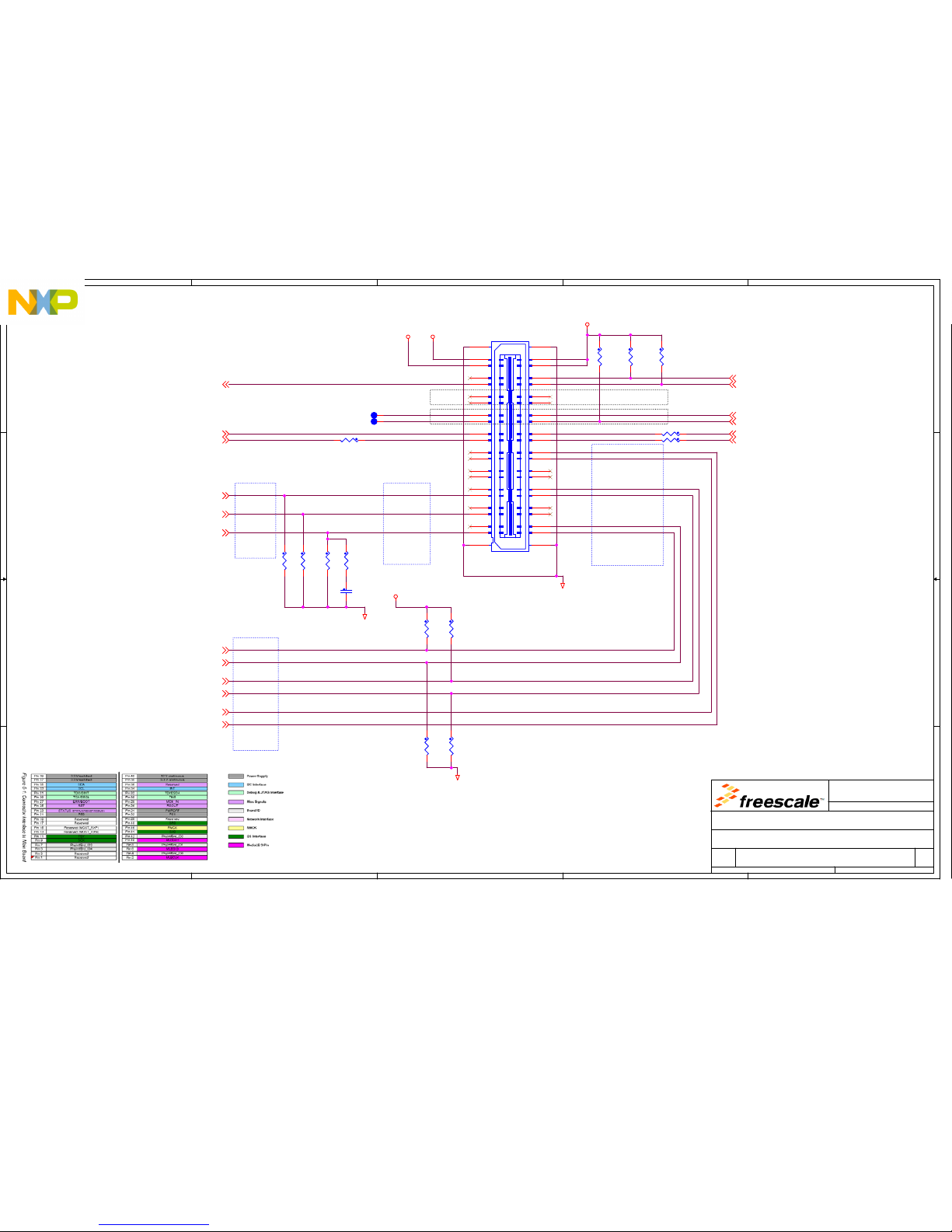
5
5
4
4
3
3
2
2
1
1
D D
C C
B B
A A
(MCK_IN)
(ID1)
(MLBSIG)
(PWROFF)
Debug - Not RQD
(ID3)
(PS1)
(ID4)
(RSVD)
(STATUS)
(ID0)
(PS0)
47 Ohm series
termination
already on
SMSC
daughtercard
Place resistors as
close as possible to
MLB tracks to
minimise stub lengths
(MLBCLK)
(RSOUT)
(MLBCP)
Parallel 100 ohm LVDS
termination and Pullups
/ Pulldopwns (DNP'd)
are already on MLB
daughtercard.
(MLBSP)
(ERR/BOOT)
(MLBCN)
(MLBSN)
(RST)
(PD[15] Shared with MLB_DAT for 3-pin mode)
(PB[15] Shared with MLB_SIG for 3-pin mode)
(PI[8] Shared with MLB_CLK for 3-pin mode)
(12v)
(3.3v Linear)
(3.3v)
(3.3v)
(MLB_PWROFF)
(RSVD)
(SR0)
(RMCK)
(SX0)
(I2C1_SDA)(SDA)
(RSVD)
(RSVD)
(I2C1_SCL)(INT)
(MLBDP)
(SCLK)
(TDO/DINT)
(TCK/DSCL)
(TDI/DSDA)
(TMS)
(MLBDN)
(ID2)
(MLBDAT)
MLB (SMSC) Daughtercard Connector
Series
termination
on MCU
daughtercard
Parallel
termination
on MCU
daughtercard
CARD INTERRUPTING MCU (WKPU21)
Controls INIC Mode
Layout Note: MLB track lengths should be < 80mm
(from MCU through daughter card to connector)
All MLB Signals are in
power domain VDD_HV_C.
The MLB interface only
supports 3.3V operation.
All I/O signals must be
3.3V. If VDD_HVC is set
to 5V, MLB MCU pads must
be left as tri-state
with no pullups.
PE1
PE0
MLB_SN
MLB_CN
MLB_CP
MLB_DP
MLB_DN
MLB_SP
MLB_RSTOUT
MLB_CLK
MLB_MCKIN
PH6
MLB_SIG
MLB_DATMLB_DAT
MLB_SIG
MLB_SN
MLB_SP
MLB_DN
MLB_DP
MLB_CN
MLB_CP
MLB_CLK
PH7
PG9
PA6
MLB_PS1
PI13
MLB_STATUS
MLB_PS0
PD13
PI12
3V3_LR
GND
GND
GND
3V3_SR
P12V
3V3_SR
PH7
4
MLB_DAT
4
MLB_SIG
4
MLB_CLK
4
MLB_SN
4
MLB_SP
4
MLB_DN
4
MLB_DP
4
MLB_CN
4
MLB_CP
4
PG94
PI13
4,16
PH6
4
PE1
4
PE0
4
PA6
4
PD13
4,12,16
PI12
4,16
Drawing Title:
Size Document Number Rev
Date: Sheet
of
Page Title:
Automotive Microcontroller
Applications
East Kilbride, Scotland
SCH-27897 PDF: SPF-27897 D1
MPC574xx Customer EVB Main Board
B
Friday, August 14, 2015
MLB SMSC Daughtercard Connector
13 16
Freescale General Business Use
Drawing Title:
Size Document Number Rev
Date: Sheet of
Page Title:
Automotive Microcontroller
Applications
East Kilbride, Scotland
SCH-27897 PDF: SPF-27897 D1
MPC574xx Customer EVB Main Board
B
Friday, August 14, 2015
MLB SMSC Daughtercard Connector
13 16
Freescale General Business Use
Drawing Title:
Size Document Number Rev
Date: Sheet of
Page Title:
Automotive Microcontroller
Applications
East Kilbride, Scotland
SCH-27897 PDF: SPF-27897 D1
MPC574xx Customer EVB Main Board
B
Friday, August 14, 2015
MLB SMSC Daughtercard Connector
13 16
Freescale General Business Use
R62 0 DNP
R51
1.0K
R55
1.0K
R52
47K
R53
619.0
1%
R57
619.0
1%
R50
100
DNP
R65
10.0K
R54
47K
R64
10.0K
C21
27PF
DNP
R63
10.0K
R60 0 DNP
TPV14
P16
QSH-020-01-L-D-DP-A
1
3
5
7
9
11
13
15
17
19
21
23
25
27
29
31
33
35
37
39
2
4
6
8
10
12
14
16
18
20
22
24
26
28
30
32
34
36
38
40
4142
4344
TPV17
R61 0 DNP
R56
47K
Page 49
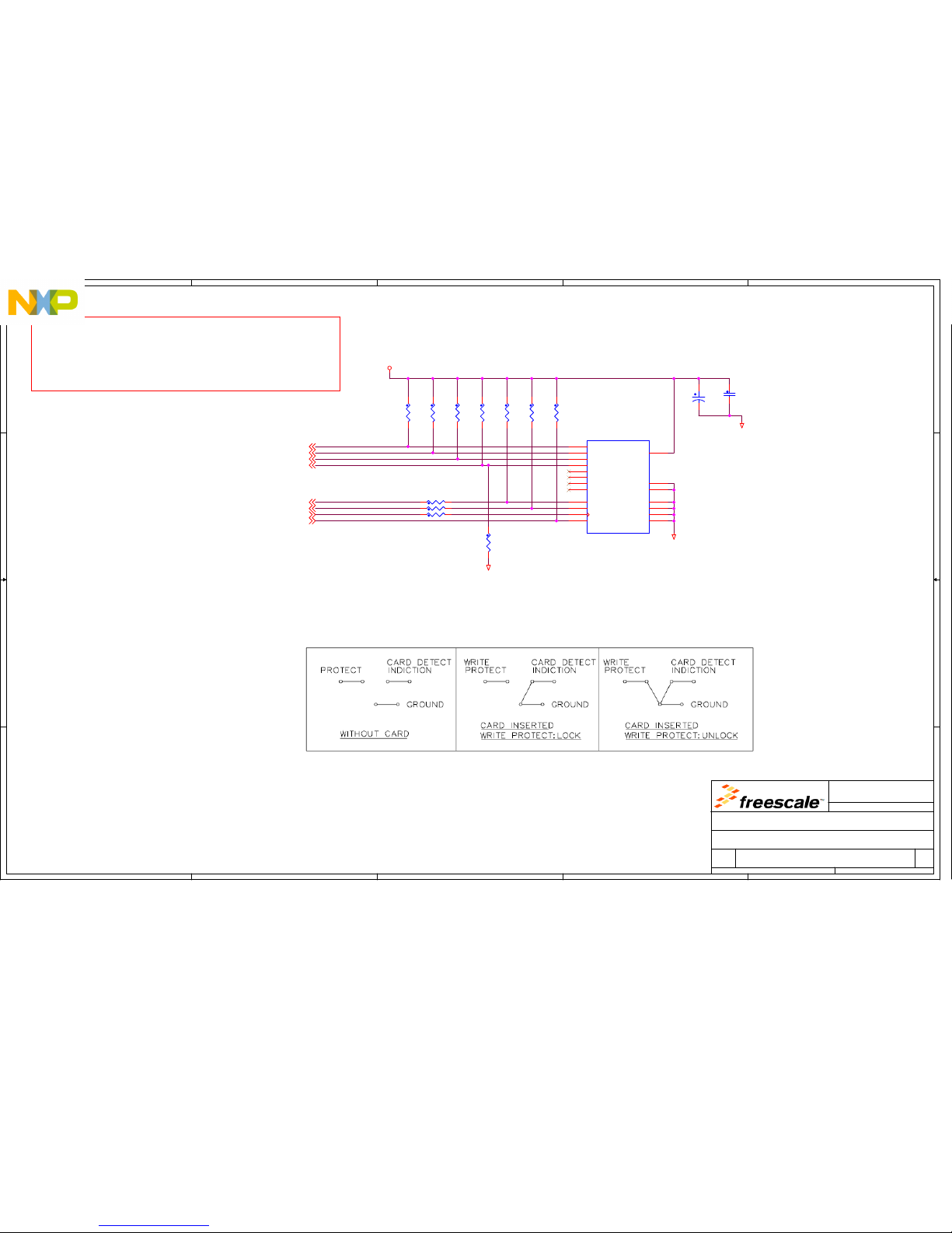
5
5
4
4
3
3
2
2
1
1
D D
C C
B B
A A
SD Connector
(SDHC_CLK)
(SDHC_CMD)
(SDHC_DATA0)
(SDHC_DATA1)
(SDHC_DATA2)
(SDHC_DATA3)
(35V
TANT)
Amphenol 101-00565-64 SD
/ MMC socket with card
detection switch.
The SD card specification details an operating voltage of
between 2.7 and 3.6V. If using the SD card, it can ONLY be
used when VDD_HV_A (and PER_HVA) jumpers are set to 3.3V.
Inserting an SD card with VDD_HV_A / PER_HVA set to 5V will
result in card damage.
Card Detect: Grounded when Card Inserted, Pulled high when card removed
Write Protect: Grounded when NOT protected, Pulled high when protected (or card removed)
(SDHC_CD) WKPU19
(SDHC_WP)
Caution
(0603
50V)
PE6
PE7
PI1
PI3
PI2
SDHC1_CLK
SD_Detect
PA0
SD_WP
PH8
PI0
GND
GND
GND
3V3_SR
PE7
4
PH8
4
PA0
4
PE64
PI3
4
PI2
4
PI1
4
PI0
4
Drawing Title:
Size Document Number Rev
Date: Sheet
of
Page Title:
Automotive Microcontroller
Applications
East Kilbride, Scotland
SCH-27897 PDF: SPF-27897 D1
MPC574xx Customer EVB Main Board
B
Friday, August 14, 2015
SD Card
14 16
Freescale General Business Use
Drawing Title:
Size Document Number Rev
Date: Sheet of
Page Title:
Automotive Microcontroller
Applications
East Kilbride, Scotland
SCH-27897 PDF: SPF-27897 D1
MPC574xx Customer EVB Main Board
B
Friday, August 14, 2015
SD Card
14 16
Freescale General Business Use
Drawing Title:
Size Document Number Rev
Date: Sheet of
Page Title:
Automotive Microcontroller
Applications
East Kilbride, Scotland
SCH-27897 PDF: SPF-27897 D1
MPC574xx Customer EVB Main Board
B
Friday, August 14, 2015
SD Card
14 16
Freescale General Business Use
R12
10.0K
DNP
R6
10.0K
R10
10.0K
DNP
R9
10.0K
DNP
R22 0
R7
10.0K
C12
0.1UF
+
C7
10UF
P200
MMC_SD_CARD
WP_SW
1
CD_SW
2
DAT1
3
DAT0
4
DAT75GND/VSS2
6
DAT6
7
CLK
8
VCC/VDD
9
VSS1
10
DAT5
11
CMD
12
DAT4
13
DAT3
14
DAT2
15
GND1
S1
GND2
S2
GND3
S3
GND4
S4
R11
10.0K
DNP
R8
10.0K
DNP
R13
10.0K
DNP
R23 0
R14
22
Page 50
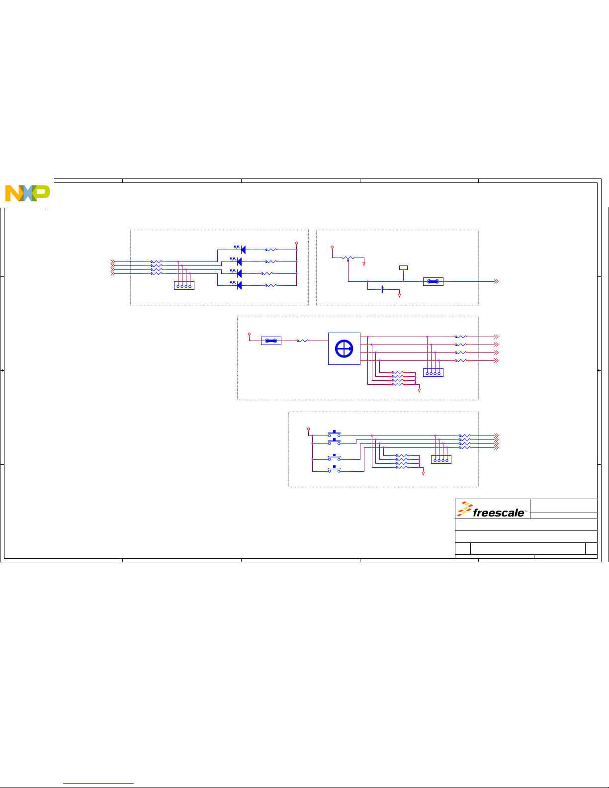
5
5
4
4
3
3
2
2
1
1
D D
C C
B B
A A
The LED's, Hex switches and push-button switches are
connected to MCU pads vvia zero ohm links. If desired
these can be removed and direct connection made to the
LED or switch. All of the ports used for LED's /
Switches are also bonded out to the GPIO matrix
Hex Encoded Switch (Active High)
Switches are hard wired to 3.3V rather than 5V so it's not possible to drive 5V into a 3.3V pad (which would cause damage)
Similarly, the LED's are active low with 3.3v supply so can be safely coupled to pads on either 3.3V or 5V domains
The ADC input is limited to 3.3V, again to prevent driving 5V into a 3.3V pad which would cause damage
PG[2..5] share eMIOS1
UC[11..14] with PWM
functionality
(eMIOS H / X)
(eMIOS G / X)
(eMIOS G / Y)
(eMIOS G)
User Pushbutton Switches (Active High)
User Peripherals, Audio Controls and GPIO
LED's are SMD (1206) Yellow
User LED's (Active Low)
OMRON B3WN-6002 Pushbutton Switch
Since the Hex switch always
has an active output, the
jumper is to allow the switch
to be powered off
ADC Input Pot and Test Point
(Note - This is run from linear 3.3v regulator to
provide a stable input voltage)
(ADC1_P[0])
(0603 50V)
Note - PA1 is also the NMI pin!
Note that LED2 and LED4 (PG3
and PG5) can be controlled in
LPU_RUN mode (and also have pad
keepers in LPU_STANDBY)
PB_SW1
PB_SW2
USR_LED4
PB_SW3
PB_SW4
USR_LED2
USR_LED1
USR_LED3
PA1
PA2
PF9
PF11
HEX_SW1
HEX_SW2
HEX_SW3
PD0
PD1
PD2
PD3
HEX_SW4
PG2
PG3
PG4
PG5
PB4
GND
3V3_SR
3V3_SR
3V3_SR
GND
3V3_LR
GND
GND
PG2
4,12,16
PG3
4,12,16
PG4
4,12,16
PG5
4,12,16
PA2
4,16
PF9
4,16
PF11
4,16
PD1
4,16
PD2
4,16
PD3
4,16
PD0
4,16
PA1
4,16
PB4
4
Drawing Title:
Size Document Number Rev
Date: Sheet
of
Page Title:
Automotive Microcontroller
Applications
East Kilbride, Scotland
SCH-27897 PDF: SPF-27897 D1
MPC574xx Customer EVB Main Board
B
Friday, August 14, 2015
User Peripherals, Audio Controls and GPIO
15 16
Freescale General Business Use
Drawing Title:
Size Document Number Rev
Date: Sheet of
Page Title:
Automotive Microcontroller
Applications
East Kilbride, Scotland
SCH-27897 PDF: SPF-27897 D1
MPC574xx Customer EVB Main Board
B
Friday, August 14, 2015
User Peripherals, Audio Controls and GPIO
15 16
Freescale General Business Use
Drawing Title:
Size Document Number Rev
Date: Sheet of
Page Title:
Automotive Microcontroller
Applications
East Kilbride, Scotland
SCH-27897 PDF: SPF-27897 D1
MPC574xx Customer EVB Main Board
B
Friday, August 14, 2015
User Peripherals, Audio Controls and GPIO
15 16
Freescale General Business Use
R277 0
DS3
AC
R257 270
R286
100
DS8
AC
R269 270
R275 0
R278 10.0K
R262 0
R258 0
C25 0.1UF
DNP
R290 10.0K
SW3
1 2
RV1 2K
13
2
R287 0
R289 0
P22
HDR 1X4
DNP
123
4
R261 270
P20
HDR 1X4
DNP
123
4
DS7
AC
R301 10.0K
R304 0
R276 10.0K
DS2
AC
R282 0
R303 10.0K
TP18
1
R281 10.0K
R280 0
P19
HDR 1X4
DNP
123
4
R260 0
R259 270
SW6
1 2
R270 0
SW4
1 2
0
3
5
1
2
4
6
7
8
9
A
B
C
D
E
F
SW2
DRS4016
C
1
2
8
4
R302 0
R288 10.0K
J26
12
SW7
1 2
R279 10.0K
J17
12
Page 51
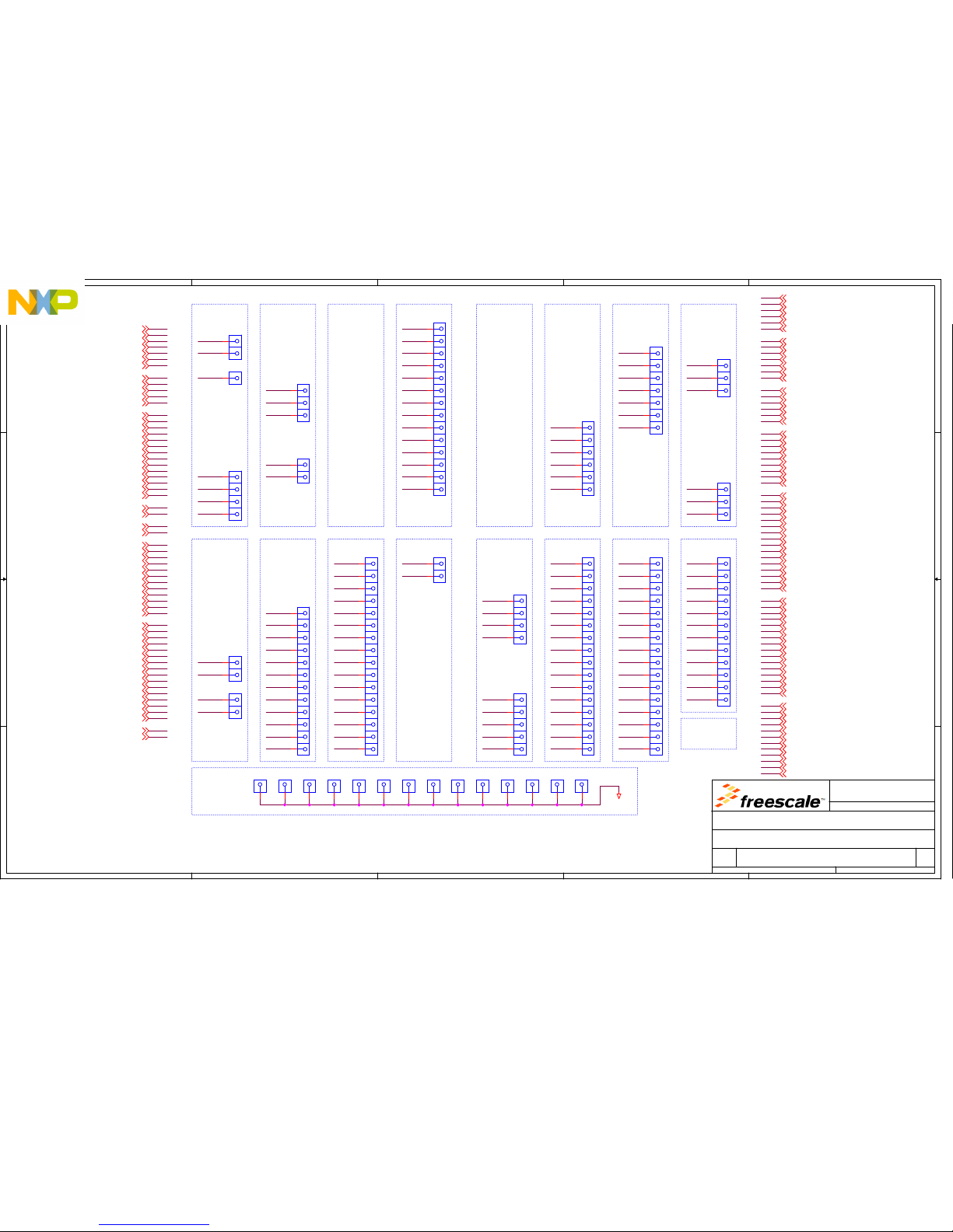
5
5
4
4
3
3
2
2
1
1
D D
C C
B B
A A
All pads are DNP (Do Not Populate) 0.1" pitch headers placed on a 0.1" grid
GPIO Pin Matrix
PORTA PORTB PORTC PORTD PORTE PORTF PORTG PORTH
PORTQ
Layout Notes:
Pads must be placed in a 13 x 16 matrix pattern, 2.54 mm pitch
- 13 wide (one column for each port EXCLUDING those with no available pads ie C, E, H, Q)
- 16 tall (1 row for each port number from 0 to 15).
- GND pad at bottom of each colum
- After production, pads should be through hole (not solder filled)
No spare pins
on PortQ
No spare pins
on PortE
PORTI PORTJ PORTK PORTL PORTM PORTN PORTO PORTP
No spare pins
on PortE
Busses are not used
on ports as it makes
it harder to see
which pins are shared
with other functions
14 GND Pads
(one at
bottom of
each colum)
PD[0..3] shared with
Hex Switch
PD[4..8] shared with
TWRPI connector with
pullup on PD[7], PD[8]
PA[1,2] shared with
user switches
PA[12..15] shared with
SAI Audio and TWRPI
PD[13] shared with
SAI Audio and MLB
headers
PI[12,13] shared with
MLB header
PK[0..4] shared with
TWRPI header
PF[9,11] shared with
user switches
PG[2..5] shared with
user LED's, SAI and
TWRPI headers
PM[3..4] shared with
SAI Audio header
PO[0..1] shared with
TWRPI header
PK0
PK1
PK3
PK2
PK4
PK7
PK8
PK9
PK11
PK10
PK12
PK13
PK14
PK15
PL0
PL1
PI9
PI10
PI12
PI13
PJ4
PJ9
PJ11
PJ10
PJ12
PJ15
PK0
PK1
PK3
PK2
PK4
PK7
PK8
PK9
PK11
PK10
PK12
PK13
PK14
PK15
PL0
PL1
PM3
PM4
PM5
PM6
PM11
PM12
PM13
PM14
PM15
PN0
PN1
PN3
PN2
PN4
PN5
PN7
PN6
PN8
PN9
PN11
PN10
PN12
PN15
PO0
PO1
PO3
PO2
PO4
PO5
PO7
PO6
PO8
PO9
PO11
PO10
PO12
PO13
PO14
PO15
PP0
PP1
PP3
PP2
PP4
PP5
PP7
PP6
PP8
PP9
PP11
PP10
PA1
PA2
PA4
PA12
PA13
PA14
PA15
PB5
PB7
PB6
PB11
PB12
PD0
PD1
PD3
PD2
PD4
PD5
PD7
PD6
PD8
PD9
PD11
PD10
PD12
PD13
PF8
PF9
PF11
PF10
PF12
PF13
PG3
PG2
PG4
PG5
PG7
PG6
PG8
PA1
PA2
PA4
PG3
PG2
PG4
PG5
PG7
PG6
PG8
PA12
PA13
PA14
PA15
PI9
PI10
PI12
PI13
PB5
PB7
PB6
PB11
PB12
PF8
PF9
PF11
PF10
PF12
PF13
PJ4
PJ9
PJ11
PJ10
PJ12
PJ15
PN13
PN14
PJ13
PJ13
PJ14
PJ14
PK5
PK6
PK5
PK6
PD0
PD1
PD3
PD2
PD4
PD5
PD7
PD6
PD8
PD9
PD11
PD10
PD12
PD13
PM3
PM4
PM5
PM6
PM11
PM12
PM13
PM14
PM15
PN0
PN1
PN3
PN2
PN4
PN5
PN7
PN6
PN8
PN9
PN11
PN10
PN12
PN15
PN13
PN14
PO0
PO1
PO3
PO2
PO4
PO5
PO7
PO6
PO8
PO9
PO11
PO10
PO12
PO13
PO14
PO15
PP0
PP1
PP3
PP2
PP4
PP5
PP7
PP6
PP8
PP9
PP11
PP10
PJ5
PJ6
PJ7
PJ8
PJ5
PJ6
PJ7
PJ8
PH15
PH14
PH13
PH13
PH14
PH15
PH3
PH4
PH5
PH5
PH4
PH3
GND
PJ4
4
PJ9
4
PJ10
4
PJ11
4
PJ12
4
PJ15
4
PK0
4,12
PK1
4,12
PK2
4,12
PK3
4,12
PK4
4,12
PK7
4
PK8
4
PK9
4
PK10
4
PK11
4
PK12
4
PK13
4
PK14
4
PK15
4
PL0
4
PL1
4
PA1
4,15
PA2
4,15
PA4
4
PA12
4,12
PA13
4,12
PA14
4,12
PA15
4,12
PB5
4
PB6
4
PB7
4
PB11
4
PB12
4
PI9
4
PI10
4
PI12
4,13
PI13
4,13
PJ13
4
PJ14
4
PK5
4
PK6
4
PD0
4,15
PD1
4,15
PD2
4,15
PD3
4,15
PD4
4,12
PD5
4,12
PD6
4,12
PD7
4,12
PD8
4,12
PD9
4
PD10
4
PD11
4
PD12
4
PD13
4,12,13
PJ5
4
PJ6
4
PJ7
4
PJ8
4
PG2
4,12,15
PG3
4,12,15
PG4
4,12,15
PG5
4,12,15
PG6
4
PG7
4
PG8
4
PF8
4
PF9
4,15
PF10
4
PF11
4,15
PF12
4
PF13
4
PM3
4,12
PM4
4,12
PM5
4
PM6
4
PM11
4
PM12
4
PM13
4
PM14
4
PM15
4
PN0
4
PN1
4
PN2
4
PN3
4
PN4
4
PN5
4
PN6
4
PN7
4
PN8
4
PN9
4
PN10
4
PN11
4
PN12
4
PN13
4
PN14
4
PN15
4
PO0
4,12
PO1
4,12
PO2
4
PO3
4
PO4
4
PO5
4
PO6
4
PO7
4
PO8
4
PO9
4
PO10
4
PO11
4
PO12
4
PO13
4
PO14
4
PO15
4
PP0
4
PP1
4
PP2
4
PP3
4
PP4
4
PP5
4
PP6
4
PP7
4
PP8
4
PP9
4
PP10
4
PP11
4
PH13
4
PH14
4
PH15
4
PH3
4
PH4
4
PH5
4
Drawing Title:
Size Document Number Rev
Date: Sheet
of
Page Title:
Automotive Microcontroller
Applications
East Kilbride, Scotland
SCH-27897 PDF: SPF-27897 D1
MPC574xx Customer EVB Main Board
B
Friday, August 14, 2015
GPIO Pin Matrix
16 16
Freescale General Business Use
Drawing Title:
Size Document Number Rev
Date: Sheet of
Page Title:
Automotive Microcontroller
Applications
East Kilbride, Scotland
SCH-27897 PDF: SPF-27897 D1
MPC574xx Customer EVB Main Board
B
Friday, August 14, 2015
GPIO Pin Matrix
16 16
Freescale General Business Use
Drawing Title:
Size Document Number Rev
Date: Sheet of
Page Title:
Automotive Microcontroller
Applications
East Kilbride, Scotland
SCH-27897 PDF: SPF-27897 D1
MPC574xx Customer EVB Main Board
B
Friday, August 14, 2015
GPIO Pin Matrix
16 16
Freescale General Business Use
TPH10
1
IOM92
1
IOM40
1
IOM118
1
IOM101
1
IOM1
1
IOM72
1
IOM45
1
IOM56
1
IOM18
1
IOM44
1
TPH7
1
IOM111
1
TPH4
1
IOM17
1
IOM70
1
IOM76
1
IOM77
1
IOM39
1
IOM102
1
IOM131
1
IOM84
1
IOM33
1
IOM7
1
IOM124
1
IOM97
1
IOM15
1
IOM96
1
IOM13
1
IOM29
1
IOM99
1
TPH15
1
IOM19
1
IOM50
1
IOM10
1
IOM81
1
TPH12
1
IOM58
1
IOM9
1
IOM126
1
IOM54
1
IOM88
1
IOM128
1
IOM98
1
IOM43
1
IOM26
1
IOM52
1
IOM105
1
IOM65
1
IOM24
1
IOM104
1
TPH9
1
IOM46
1
IOM67
1
IOM48
1
IOM91
1
IOM6
1
IOM21
1
IOM89
1
IOM123
1
IOM5
1
TPH6
1
IOM103
1
IOM73
1
IOM28
1
TPH3
1
IOM109
1
IOM62
1
IOM63
1
IOM115
1
IOM41
1
IOM4
1
IOM53
1
IOM85
1
IOM119
1
IOM106
1
IOM90
1
IOM32
1
IOM95
1
IOM16
1
IOM34
1
IOM83
1
IOM60
1
IOM108
1
IOM51
1
IOM14
1
IOM82
1
IOM87
1
TPH14
1
IOM8
1
IOM116
1
IOM27
1
IOM38
1
IOM80
1
IOM35
1
TPH11
1
IOM121
1
IOM49
1
IOM110
1
TPH8
1
IOM129
1
IOM31
1
IOM2
1
IOM112
1
IOM78
1
IOM79
1
IOM107
1
IOM25
1
IOM69
1
IOM75
1
IOM130
1
IOM93
1
IOM94
1
IOM132
1
IOM42
1
IOM37
1
IOM114
1
IOM59
1
TPH5
1
IOM30
1
IOM125
1
IOM20
1
IOM47
1
IOM64
1
IOM12
1
TPH2
1
IOM3
1
IOM127
1
IOM100
1
IOM117
1
IOM113
1
IOM36
1
IOM71
1
IOM11
1
IOM61
1
IOM68
1
IOM122
1
IOM66
1
IOM57
1
TPH13
1
IOM55
1
IOM74
1
IOM23
1
IOM86
1
IOM22
1
IOM120
1
Page 52

324 BGA DC
Page 53
5
5
4
4
3
3
2
2
1
1
D D
C C
B B
A A
X5
Freescale AISG Applications, East Kilbride
X2
X3
X4
Revision Information
Designer CommentsRev Date
GPIO - MPC5748G GPIO pins 1 of 2
Clocks
Sheet 8
Sheet 2
Sheet 3
Sheet 4
Sheet 5
Sheet 6
Sheet 7
GPIO - MPC5748G GPIO pins 2 of 2
Table Of Contents:
MPC5748G Customer EVB 324 BGA Daughter Card (MPC574XG-324DS)
X1
Power - MPC5748G power pins footprint
Power - MPC5748G Decoupling Capacitors
Daughtercard Connectors
Bus Termination
28 Feb 2013 Alasdair Robertson Initial release sent for review
These schematics are provided for reference purposes only. As such,
Freescale does not make any warranty, implied or otherwise, as to the
suitability of circuit design or component selection (type or value) used in
these schematics for hardware design using the Freescale MPC5748G family
of Microprocessors. Customers using any part of these schematics as a
basis for hardware design, do so at their own risk and Freescale does not
assume any liability for such a hardware design.
User notes are given throughtout the schematics.
Specific PCB LAYOUT notes are detailed in ITALICS
Caution:
Notes:
- All components and board processes are to be ROHS compliant
- All small capacitors are 0402 unless otherwise stated
- All resistors are 0603 5% 0.1w unless otherwise stated. All zero ohm links are 0603
- All connectors and headers are denoted Px and are 2.54mm pitch unless otherwise stated
- All jumpers are denoted Jx. Jumpers are 2mm pitch
- Jumper default positions are shown in the schematics. For 3 way jumpers, default is always posn 1-2.
2 Pin jumpers generally have the "source" on pin 1.
- All switches are denoted SWx
- All test points are denoted TPx
- Test point Vias are denoted TPVx
Alasdair Robertson
Version sent to Pre Layout, incorporating fixes from review
Final Review11 Mar 2013
13 Mar 2013 Alasdair Robertson
15 Mar 2013 Alasdair Robertson Component consolodation, Few minor changes. Sent to Layout
3 Different test points used in design:
TPVx - Through Hole Pad small
TPHx - Through Hile Pad Large (for standard 0.1" header).
TPX - Surface Mount Wire Loop
Alasdair Robertson Post Layout (Back Annotated). Matches PCB RevA
Changes made during layout to Daughtercard ConnectorsAlasdair Robertson
A
29 Mar 2013
Alasdair Robertson CIS CAD Database update & SCH Back-Annotate15 Apr 2013X6
15 Apr 2015
A1 18 Aug 2015 Alasdair Robertson Tidy up Schematics for UM (RevA PCB)
Drawing Title:
Size Document Number Rev
Date: Sheet
of
Page Title:
Designer:
Drawn by:
Approved:
Automotive Microcontroller Applications
East Kilbride, Scotland
This document contains information proprietary to Freescale and shall not be used for engineering design,
procurement or manufacture in whole or in part without the express written permission of Freescale
SCH-27900 PDF: SPF-27900 A1
MPC5748G 324 BGA Daughter Card
B
Tuesday, August 18, 2015
Index and Title Page
A. Robertson
A. Robertson
A. Robertson
18
Freescale General Business Use
Drawing Title:
Size Document Number Rev
Date: Sheet
of
Page Title:
Designer:
Drawn by:
Approved:
Automotive Microcontroller Applications
East Kilbride, Scotland
This document contains information proprietary to Freescale and shall not be used for engineering design,
procurement or manufacture in whole or in part without the express written permission of Freescale
SCH-27900 PDF: SPF-27900 A1
MPC5748G 324 BGA Daughter Card
B
Tuesday, August 18, 2015
Index and Title Page
A. Robertson
A. Robertson
A. Robertson
18
Freescale General Business Use
Drawing Title:
Size Document Number Rev
Date: Sheet
of
Page Title:
Designer:
Drawn by:
Approved:
Automotive Microcontroller Applications
East Kilbride, Scotland
This document contains information proprietary to Freescale and shall not be used for engineering design,
procurement or manufacture in whole or in part without the express written permission of Freescale
SCH-27900 PDF: SPF-27900 A1
MPC5748G 324 BGA Daughter Card
B
Tuesday, August 18, 2015
Index and Title Page
A. Robertson
A. Robertson
A. Robertson
18
Freescale General Business Use
Page 54
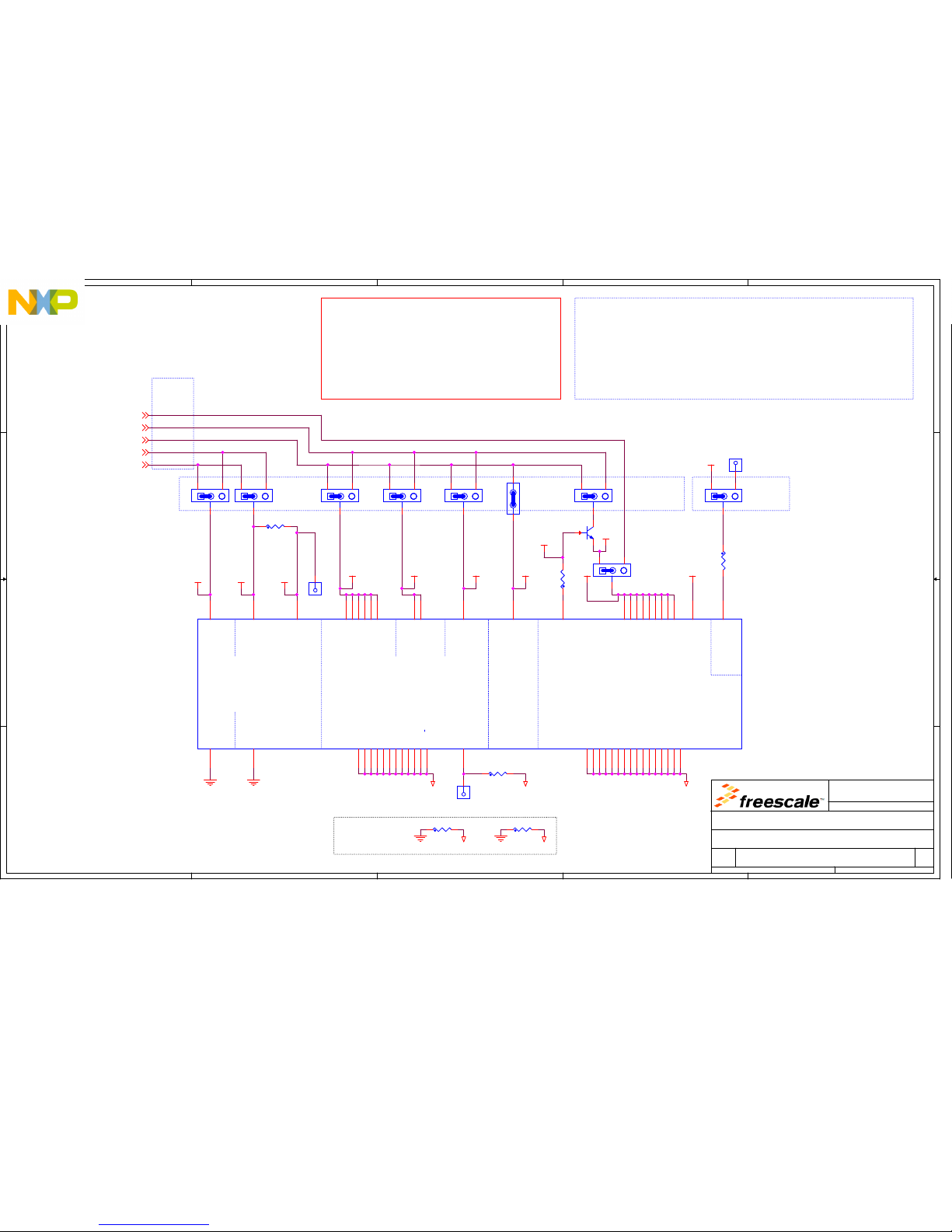
5
5
4
4
3
3
2
2
1
1
D D
C C
B B
A A
Individual MCU
supply control
jumpers
3v3
Default Configuraiton:
- ALL MCU supply voltages are set to 3.3V (ADC0, ADC1, VDD_HV_A,
VDD_HV_B, VDD_HV_C, VBallast)
- VDD_HV_FLA = External 3.3V supplied (jumper fitted)
- VDD_LV Supplied from ballast transistor
This is not necessarily the same as the default shown in the RM. All
VDD_HV_x domains have at least one peripheral that only functions at
3.3V. Therefore the default is to run these from 3.3V. The analogue pins
can only be driven to the same voltage as the VDD_HV_x domain they are
situated in (ie max 3.3V) so makes sense for the analogue supply and
reference to be 3.3V
Ground Links
(0 Ohm
Resistors)
DAC External
Ref Voltage
Select
3v3 5v0 5v0 5v0 5v0 5v03v3 3v3 3v3
3v3
3v3 5v0
(Current Limit Resistor to
protecxt against case when
other MCU supplies are
disconnected and external
reference supply is live)
MPC5748G MCU Power Connections
Caution:
- If VDD_HV_A is driven from 5V, the VDD_HV_FLA pin
must not be supplied from 3.3V (remove the HVA_FLA
jumper)
- Don't attempt to over drive an analogue pad to 5V
when the digital VDD_HV_x supply is set to 3.3V. This
will trigger the ESD protectrion on that pad. For
example if VDD_HV_A is set to 3.3V and the analogue
supplies are set to 5V, you cannot drive 5V into a
pad in the VDD_HV_A domain
From MCU
supply
jumpers on
main board
MCU_3V3_S
MCU_5V0_S
MCU_1V25_L
MCU_3V3_L
MCU_5V0_L
HVB_CAP
HVC_CAP
HVFLA_CAP
LV_CAP
ADC0_CAP
ADC1_CAP
ADC1REF_CAP
ADC0_GND ADC1_GND GND
HVA_CAP
GNDADC0_GND GNDADC1_GND
E_CAP
B_CAP
LVDEC_CAP
HVA_CAP
GND GND
MCU_1V25_L8
MCU_5V0_S8
MCU_3V3_S8
MCU_5V0_L8
MCU_3V3_L8
Drawing Title:
Size Document Number Rev
Date: Sheet
of
Page Title:
Automotive Microcontroller
Applications
East Kilbride, Scotland
SCH-27900 PDF: SPF-27900 A1
MPC5748G 324 BGA Daughter Card
B
Tuesday, August 18, 2015
MPC5748G MCU Power
28
Freescale General Business Use
Drawing Title:
Size Document Number Rev
Date: Sheet of
Page Title:
Automotive Microcontroller
Applications
East Kilbride, Scotland
SCH-27900 PDF: SPF-27900 A1
MPC5748G 324 BGA Daughter Card
B
Tuesday, August 18, 2015
MPC5748G MCU Power
28
Freescale General Business Use
Drawing Title:
Size Document Number Rev
Date: Sheet of
Page Title:
Automotive Microcontroller
Applications
East Kilbride, Scotland
SCH-27900 PDF: SPF-27900 A1
MPC5748G 324 BGA Daughter Card
B
Tuesday, August 18, 2015
MPC5748G MCU Power
28
Freescale General Business Use
J11
123
Q20
MJD31CT4
3 4
1
J3
123
J10
123
R10
0
J7
123
TPH2
1
J5
123
TPH3
1
TPH1
1
J6
123
J4
123
R36
1.0K
1.25v Core & External BallastAnalogue
MPC5748G 6M 324BGA
Package 2of3 Power Pins
Flash
DAC Ref
U1B
MPC5748G + OTB-324R-1.0-019-00
VRC_CTRL
K2
VSS_LV_F6F6VSS_LV_J7J7VSS_LV_J8J8VSS_LV_J9J9VSS_LV_K7K7VSS_LV_K8K8VSS_LV_K9K9VSS_LV_K10
K10
VSS_LV_L7L7VSS_LV_L8L8VSS_LV_L9L9VSS_LV_L10
L10
VSS_LV_M7M7VSS_LV_M8M8VSS_LV_M9M9VSS_LV_M10
M10
VDD_LV_D8
D8
VDD_LV_F5
F5
VDD_LV_K3
K3
VDD_LV_K11
K11
VDD_LV_K12
K12
VDD_LV_L11
L11
VDD_LV_L12
L12
VDD_LV_M11
M11
VDD_LV_M12
M12
VDD_HV_A_C2C2VDD_HV_A_C9C9VDD_HV_A_R7
R7
VDD_HV_A_E18
E18
VDD_HV_A_K17
K17
VDD_HV_A_U8
U8
VDD_HV_B_J15
J15
VDD_HV_B_K13
K13
VDD_HV_C
L14
VSS_HV_ADC0
U14
VDD_HV_ADC0
V14
VDD_HV_ADC1
V16
VSS_HV_ADC1
V17
VDD_HV_FLA
J2
VDD_HV_ADC1_REF
V15
VSS_HV_H7H7VSS_HV_H8H8VSS_HV_H9H9VSS_HV_H10
H10
VSS_HV_H11
H11
VSS_HV_H12
H12
VSS_HV_J10
J10
VSS_HV_J11
J11
VSS_HV_J12
J12
VSS_HV_K14
K14
VSS_HV_K16
K16
VSS_HV_V8
V8
VIN1_CMP_REF
J3
VDD_LP_DEC
L2
VSS_HV_VPP
K1
R9
0
R7
0
J8
12
R35
0
J9
123
R24
0
Page 55
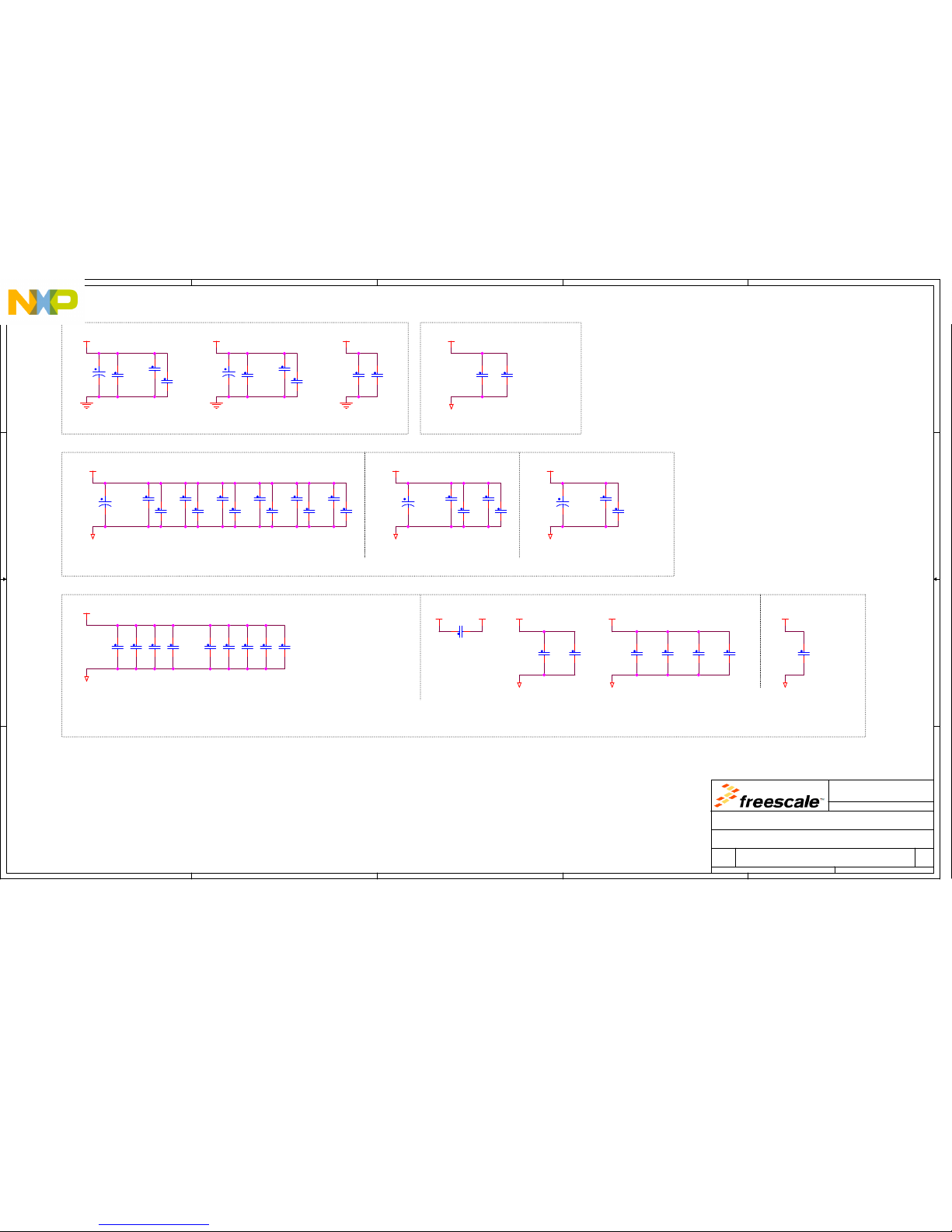
5
5
4
4
3
3
2
2
1
1
D D
C C
B B
A A
Capacitor Types:
470pF - Ceramic COG, 50v 5% 0402
1000pF - Ceramic COG, 50V 5% 0402
4700pF - Ceramic X7R, 50V 10% 0402
0.01uF - Ceramic X7R, 50V 10% 0402
0.1uF - Ceramic X7R, 16V 10% 0402
0.68uF - Ceramic X7R 16V 10% 0805 (Murata GCM219R71C684KA37 )
1.0uF - Ceraminc X7R, 10V 10% 0603 (Taiyo Yuden LMK107B7105KA-T)
2.2uF - Ceraminc X7R, 10V, 10%, 0603 (Taiyo Yuden LMK107B7225KA-TR)
4.7uF - TANT, 12.5V 20% ESR=0.08R 7343
10uF - TANT, 35V 10% ESR=0.125R CC7343-31
4.7uF Alternative (150-78844)- Polymer ALU, 16V 20% ESR=0.08R
7343-18
Place small Caps as close as possible to MCU pins
ADC
Place small caps close to each MCU pin
VDD_HVA VDD_HVB VDD_HVC
VDD_LV
See caps below for Bypass Transistor bulk storage (some on VDD1V2 rail)
VDD_LV (1.25V) Decoupling. Place one of the non DNP caps each side of the device
as close as possible to pin. Distribute other (DNP) caps around rest of pins
Ballast Transistor
Flash
MPC5748G MCU Decoupling and bulk storage
LP Internal Reg Cap
Place
close to
transistor
Place one 0.68uF cap footprint
each side of package
Place 10uF cap to west side of package
(low ESR)
(low
ESR)
(low
ESR)
(Murata GCM219R71C684KA37)
(low
ESR)
(low
ESR)
(low
ESR)
(low
ESR)
(low ESR)
2.2uF caps
are DNP.
Place close
to emitter
One of these is DNP. May replace 2 caps with
0.47uF to keep overall capacitance within limits
ADC0_CAP
ADC0_GND
ADC1REF_CAP
ADC1_GND
ADC1_CAP
ADC1_GND
GND
HVA_CAP
GND
HVB_CAP
GND
HVC_CAP
LV_CAP
GND
HVFLA_CAP
GND
LV_CAPB_CAP E_CAP
GND
LVDEC_CAP
GND
E_CAP
GND
Drawing Title:
Size Document Number Rev
Date: Sheet
of
Page Title:
Automotive Microcontroller
Applications
East Kilbride, Scotland
SCH-27900 PDF: SPF-27900 A1
MPC5748G 324 BGA Daughter Card
B
Tuesday, August 18, 2015
MPC5748G MCU Decoupling
38
Freescale General Business Use
Drawing Title:
Size Document Number Rev
Date: Sheet of
Page Title:
Automotive Microcontroller
Applications
East Kilbride, Scotland
SCH-27900 PDF: SPF-27900 A1
MPC5748G 324 BGA Daughter Card
B
Tuesday, August 18, 2015
MPC5748G MCU Decoupling
38
Freescale General Business Use
Drawing Title:
Size Document Number Rev
Date: Sheet of
Page Title:
Automotive Microcontroller
Applications
East Kilbride, Scotland
SCH-27900 PDF: SPF-27900 A1
MPC5748G 324 BGA Daughter Card
B
Tuesday, August 18, 2015
MPC5748G MCU Decoupling
38
Freescale General Business Use
C51
0.1UF
DNP
C26
0.1UF
C42
1000pF
C30
0.1UF
C48
1000pF
C61
0.68uF
C40
470pF
C24
0.1UF
C50
0.1UF
C59
1.0 UF
C44
0.1UF
C25
0.1UF
DNP
C32
0.1UF
C34
2.2UF
LMK107B7225KA-T
C53
0.1UF
C29
0.68uF
C46
0.1UF
DNP
C43
1uF
LMK107B7105KA-T
C35
0.1UF
C10
2.2UF
DNP
C28
470pF
C33
1000pF
C52
1000pF
C49
1000pF
C23
0.1UF
C20
0.68uF
DNP
C57
0.1UF
C39
0.1UF
+
C4
10UF
DNP
C55
1000pF
C58
1.0 UF
C56
0.1UF
+
C1
10UF
C54
0.1UF
C36
1000pF
C47
1000pF
C9
2.2UF
DNP
+
C2
10UF
DNP
C60
1.0 UF
C8 4700pF
C38
0.1UF
+
C3
10UF
DNP
C41
0.1UF
C31
0.68uF
C27
470pF
C21
0.1UF
DNP
C22
470pF
+
C5
10UF
DNP
C37
1000pF
C45
0.1UF
DNP
Page 56
5
5
4
4
3
3
2
2
1
1
D D
C C
B B
A A
MPC5748G GPIO 1 of 2
Key to text colours:
Purple - Comms Physical Interfaces
Blue - Debug (JTAG & Nexus)
(LIN0_RX)
(LIN0_TX)
(LIN1_TX)
(LIN1_RX)
(XTAL32)
(EXTAL32)
(FR_A_TX)
(FR_A_TX_EN)
(FR_A_RX)
(FR_B_TX_EN)
(FR_B_RX)
(FR_B_TX)
(USB1_CLK)
(USB1_D0)
(USB1_D1)
(USB1_D2)
(USB1_D3)
(USB1_D4)
(USB1_D5)
(USB1_D6)
(USB1_D7)
(USB1_DIR)
Orange - Other Peripherals and I/O
(RMII_RXD0)
(RMII_RXD1)
(MII_RXD2)
(MII_RXD3)
(MII_CRS)
(RMII_TXD0)
(RMII_TXD1)
(MII_TXD2)
(MII_TXD3)
(RMII_TXEN)
(RMII_MDC)
(RMII_TXCLK)
(RMII_RXDV)
(RMII_MDIO)
(RMII_RXER)
(MII_COL)
(MII_RXCLK)
(FR_DBG0)
(FR_DBG1)
(FR_DBG2)
(FR_DBG3)
(SD_CMD)
(SD_CLK)
(SD_WP)
(SAI0_D0)
(SAI0_D1)
(SAI0_D2)
(SAI0_D3)
(SAI0_BCLK)
(SAI0_MCLK)
(SAI0_SYNC)
(SAI1_SYNC)
(SAI1_MCLK)
(TDI)
(TDO)
(TCK)
(TMS)
Black - Clock, Reset and Control
(MLB_DN)
(MLB_DP)
(MLB_SN)
(MLB_SP / DAT)
(MLB_CN / SIG)
(SAI_I2C2_SCL)
(SAI_I2C2_SDA)
(SAI_I2C3_SDA)
(SAI_I2C3_SCL)
(MLB_I2C1_SCL)
(MLB_I2C1_SDA)
Green - I/O Matrix (dedicated)
(CMP1_8 / IO)
(CMP1_10 / IO)
(CMP1_11 /IO)
(CMP1_12 / IO)
(CMP1_13 / IO)
(CMP1_14 / IO)
(CMP1_15 / IO)
(CLKOUT1 GPIO)
(GPIO)
(GPIO)
(HEX1 & GPIO)
(HEX2 & GPIO)
(HEX3 & GPIO)
(HEX4 & GPIO)
(SW1 & GPIO**)
(SW2 & GPIO)
(LED1 & GPIO)
(LED2 & GPIO)
(LED3 & GPIO)
(LED4 & GPIO)
(MLB_RST)
(MLB_PWR)
(MLB_IRQ - WKPU21)
** PA1 is also NMI. Routed
to I/O Matrix
RED - I/O Matrix and other functions (eg LED)
(CLKOUT0 GPIO)
(eMIOS1_UC_5H)
(eMIOS1_UC_6H)
(eMIOS1_UC_7H)
(ADC_POT)
(GPIO)
(GPIO)
(GPIO)
(GPIO)
(GPIO)
(GPIO)
(GPIO)
(GPIO)
(GPIO)
(GPIO)
(GPIO)
(GPIO)
(GPIO)
(GPIO)
(GPIO)
(CAN0_TX)
(CAN0_RX)
(SW4 & GPIO)
(CAN1_RX)
(CAN1_TX)
(SW3 & GPIO)
(RS232_RX)
(RS232_TX)
(SD_CD - WKPU19)
(GPIO)
(GPIO)
(GPIO)
(eMIOS E1UC_11_H)
(eMIOS E1UC_12_H)
(eMIOS E1UC_13_H)
(eMIOS E1UC_14_H)
(WKPU2 / NMI0)
(WKPU3)
WKPU22
WKPU15
(SAI_GPIO)
(MLB_GPIO)
(GPIO & MLB_ST)
PA0
PA1
PA3
PA2
PA4
PA5
PA7
PA6
PA8
PA9
PA11
PA10
PA12
PA13
PA15
PA14
PB0
PB1
PB3
PB2
PB4
PB5
PB7
PB6
PB8
PB9
PB11
PB10
PB12
PB13
PB15
PB14
PC0
PC1
PC3
PC2
PC4
PC5
PC7
PC6
PC8
PC9
PC11
PC10
PC12
PC13
PC15
PC14
PD0
PD1
PD3
PD2
PD4
PD5
PD7
PD6
PD8
PD9
PD11
PD10
PD12
PD13
PD15
PD14
PE0
PE1
PE3
PE2
PE4
PE5
PE7
PE6
PE8
PE9
PE11
PE10
PE12
PE13
PE15
PE14
PF0
PF1
PF3
PF2
PF4
PF5
PF7
PF6
PF8
PF9
PF11
PF10
PF12
PF13
PF15
PF14
PG0
PG1
PG3
PG2
PG4
PG5
PG7
PG6
PG8
PG9
PG11
PG10
PG12
PG13
PG15
PG14
PH0
PH1
PH3
PH2
PH4
PH5
PH7
PH6
PH8
PH9
PH11
PH10
PH12
PH13
PH15
PH14
MCU-EXTAL
MCU-XTAL
PORSTx
MCU-RSTx
PH0
7
PORSTx
8
MCU-RSTx8
MCU-EXTAL
6
MCU-XTAL6
PB08
PB18
PB28
PB38
PB118
PB128
PB137
PB147
PB157
PB68
PB78
PB86
PB96
PB108
PA118
PA128
PA138
PA148
PA158
PA68
PA78
PA88
PA98
PA108
PA58
PA08
PA18
PA28
PA38
PA48
PB58
PB48
PC118
PC128
PC138
PC148
PC158
PC68
PC78
PC88
PC98
PC108
PC58
PC48
PC08
PC18
PC28
PC38
PD118
PD128
PD138
PD147
PD157
PD68
PD78
PD88
PD98
PD108
PD58
PD48
PD08
PD18
PD28
PD38
PH1
7
PH2
7
PH3
8
PH4
8
PH5
8
PH6
8
PH7
8
PH8
8
PH9
8
PH10
8
PH11
8
PH12
8
PH13
8
PH14
8
PH15
8
PG0
7
PG1
8
PG2
8
PG3
8
PG4
8
PG5
8
PG6
8
PG7
8
PG8
8
PG9
8
PG10
8
PG11
8
PG12
7
PG13
7
PG14
8
PG15
8
PF0
8
PF1
8
PF2
8
PF3
8
PF4
8
PF5
8
PF6
8
PF7
8
PF8
8
PF9
8
PF10
8
PF11
8
PF12
8
PF13
8
PF14
8
PF15
8
PE0
8
PE1
8
PE2
8
PE3
8
PE4
8
PE5
8
PE6
8
PE7
8
PE8
8
PE9
8
PE10
8
PE11
8
PE12
8
PE13
8
PE14
8
PE15
8
Drawing Title:
Size Document Number Rev
Date: Sheet
of
Page Title:
Automotive Microcontroller
Applications
East Kilbride, Scotland
SCH-27900 PDF: SPF-27900 A1
MPC5748G 324 BGA Daughter Card
B
Tuesday, August 18, 2015
MPC5748G GPIO 1of2
48
Freescale General Business Use
Drawing Title:
Size Document Number Rev
Date: Sheet of
Page Title:
Automotive Microcontroller
Applications
East Kilbride, Scotland
SCH-27900 PDF: SPF-27900 A1
MPC5748G 324 BGA Daughter Card
B
Tuesday, August 18, 2015
MPC5748G GPIO 1of2
48
Freescale General Business Use
Drawing Title:
Size Document Number Rev
Date: Sheet of
Page Title:
Automotive Microcontroller
Applications
East Kilbride, Scotland
SCH-27900 PDF: SPF-27900 A1
MPC5748G 324 BGA Daughter Card
B
Tuesday, August 18, 2015
MPC5748G GPIO 1of2
48
Freescale General Business Use
MPC5748G 324 BGA
Package 1of3 GPIO Pins1
U1A
MPC5748G + OTB-324R-1.0-019-00
PB0
N1
PB1
N2
PB2
G9
PB3
G8
PB4
N11
PB5
R14
PB6
N12
PB7
P14
PB8/XTAL32
V10
PB9/EXTAL32
V9
PB10
P9
PB11
P13
PB12
N13
PB13
T18
PB14
R17
PB15
R18
PC0
F9
PC1
F10
PC2
C13
PC3
D11
PC4
B12
PC5
A11
PC6
R3
PC7
U2
PC8
D5
PC9
D4
PC10
M5
PC11
M4
PC12
D6
PC13
E6
PC14
B2
PC15
C3
PD0
R12
PD1
T13
PD2
T14
PD3
R13
PD4
P11
PD5
T15
PD6
U15
PD7
R15
PD8
P12
PD9
N15
PD10
P15
PD11
V18
PD12
N16
PD13
N14
PD14
T17
PD15
P17
PE0
H3
PE1
H2
PE2
A12
PE3
D10
PE4
B11
PE5
A10
PE6
F8
PE7
D7
PE8
K5
PE9
K4
PE10
H1
PE11
J1
PE12
C18
PE13
G17
PE14
C15
PE15
E12
PF0
N9
PF1
R9
PF2
P10
PF3
U10
PF4
N10
PF5
V12
PF6
T11
PF7
R10
PF8
T2
PF9
T1
PF10
R5
PF11
P5
PF12
N5
PF13
N6
PF14
G18
PF15
H17
PG0
H18
PG1
J16
PG2
J4
PG3
J5
PG4
G2
PG5
F2
PG6
M2
PG7
M1
PG8
M3
PG9
L3
PG10
D14
PG11
D13
PG12
L18
PG13
M18
PG14
F12
PG15
C16
PH0
L17
PH1
K18
PH2
J18
PH3
J17
PH4
C10
PH5
B10
PH6
A9
PH7
D9
PH8
E8
PH9
E9
PH10
E10
PH11
C14
PH12
D12
PH13
F3
PH14
E2
PH15
G4
RESET
L1
PORST
C12
XTAL
V6
EXTAL
V7
PA0
L5
PA1
K6
PA2
J6
PA3
M17
PA4
P6
PA5
A14
PA6
A13
PA7
F17
PA8
F18
PA9
E17
PA10
D18
PA11
D17
PA12
N8
PA13
P7
PA14
T3
PA15
N7
Page 57
5
5
4
4
3
3
2
2
1
1
D D
C C
B B
A A
MPC5748G GPIO 2 of 2
(USB1_NXT)
(USB1_STP)
(USB0_CLK)
(USB0_D0)
(USB0_D1)
(USB0_D2)
(USB0_D3)
(USB0_D4)
(USB0_D5)
(USB0_D6)
(USB0_D7)
(USB0_NXT)
(USB0_DIR)
(USB0_STP)
(SD_D3)
(SD_D2)
(SD_D1)
(SD_D0)
(SAI1_D0)
(SAI1_BCLK)
(SAI2_D0)
(SAI2_BCLK)
(SAI2_MCLK)
(SAI2_SYNC)
(MDO0)
(MDO1)
(MDO2)
(MDO3)
(MDO4)
(MDO5)
(MDO6)
(MDO7)
(MDO8)
(MDO9)
(MDO10)
(MDO11)
(MDO12)
(MDO13)
(MDO14)
(MDO15)
(EVTI)
(MSEO0)
(MSEO1)
(MCKO)
(EVTO)
(MLB_CP / CLK)
(GPIO)
(GPIO)
(GPIO)
(GPIO)
(GPIO)
(GPIO)
(GPIO)
(GPIO)
(GPIO)
(GPIO)
(GPIO)
(GPIO)
(GPIO)
(GPIO)
(GPIO)
(GPIO)
(GPIO)
(GPIO)
(GPIO)
(GPIO)
(GPIO)
(GPIO)
(GPIO)
(GPIO)
(GPIO)
(GPIO)
(GPIO)
(GPIO)
(GPIO)
(GPIO)
(GPIO)
(GPIO)
(GPIO)
(GPIO)
(GPIO)
(GPIO)
(GPIO)
(GPIO)
(GPIO)
(GPIO)
(GPIO)
(GPIO)
(GPIO)
(GPIO)
(GPIO)
(GPIO)
(GPIO)
(GPIO)
(GPIO)
(GPIO)
(GPIO)
(GPIO)
(GPIO)
(GPIO)
(GPIO)
(GPIO)
(GPIO)
(GPIO)
(GPIO)
(GPIO)
(GPIO)
(GPIO)
(GPIO)
(GPIO)
(GPIO)
(GPIO)
(GPIO)
(GPIO)
(GPIO)
(GPIO)
(GPIO)
(GPIO)
(GPIO)
(GPIO)
(GPIO)
(GPIO)
(GPIO)
(GPIO)
(GPIO)
(GPIO)
(GPIO)
RED - I/O Matrix and other functions (eg LED)
Blue - Debug (JTAG & Nexus)
Purple - Comms Physical Interfaces
Key to text colours:
Green - I/O Matrix (dedicated)
Black - Clock, Reset and Control
Orange - Other Peripherals and I/O
(GPIO)
(GPIO)
(GPIO)
(GPIO)
(USB1_RST)
(USB0_RST)
(ENET_RST)
(GPIO & MLB_PS0)
(GPIO & MLB_PS1)
PI0
PI1
PI3
PI2
PI4
PI5
PI7
PI6
PI8
PI9
PI11
PI10
PI12
PI13
PI15
PI14
PJ0
PJ1
PJ3
PJ2
PJ4
PJ7
PJ6
PJ8
PJ9
PJ11
PJ10
PJ12
PJ13
PJ15
PJ14
PK0
PK1
PK3
PK2
PK4
PK5
PK7
PK6
PK8
PK9
PK11
PK10
PK12
PK13
PK14
PL0
PL1
PL3
PL4
PL5
PL7
PL6
PL8
PL9
PL11
PL10
PL12
PL13
PL15
PL14
PM0
PM1
PM3
PM2
PM4
PM5
PM7
PM6
PM8
PM9
PM11
PM10
PM12
PM13
PM15
PM14
PN0
PN1
PN3
PN2
PN4
PN5
PN7
PN6
PN8
PN9
PN11
PN10
PN12
PN13
PN15
PN14
PO0
PO1
PO3
PO2
PO4
PO5
PO7
PO6
PO8
PO9
PO11
PO10
PO12
PO13
PO15
PO14
PP0
PP1
PP3
PP2
PP4
PP5
PP7
PP6
PP8
PP9
PP11
PP10
PP12
PP13
PP15
PP14
PK15
PL2
PQ1
PQ3
PQ2
PQ4
PQ5
PQ6
PJ5
PQ7
PQ0
PI118
PI128
PI138
PI148
PI158
PI68
PI78
PI87
PI98
PI108
PI58
PI08
PI18
PI28
PI38
PI48
PJ118
PJ128
PJ138
PJ148
PJ158
PJ68
PJ78
PJ88
PJ98
PJ108
PJ58
PJ08
PJ18
PJ28
PJ38
PJ48
PK118
PK128
PK138
PK148
PK158
PK68
PK78
PK88
PK98
PK108
PK58
PK08
PK18
PK28
PK38
PK48
PL118
PL128
PL138
PL148
PL158
PL68
PL78
PL88
PL98
PL108
PL58
PL08
PL18
PL28
PL38
PL48
PM0
8
PM1
8
PM2
8
PM3
8
PM4
8
PM5
8
PM6
8
PM7
8
PM8
8
PM9
8
PM10
8
PM11
8
PM12
8
PM13
8
PM14
8
PM15
8
PN0
8
PN1
8
PN2
8
PN3
8
PN4
8
PN5
8
PN6
8
PN7
8
PN8
8
PN9
8
PN10
8
PN11
8
PN12
8
PN13
8
PN14
8
PN15
8
PO0
8
PO1
8
PO2
8
PO3
8
PO4
8
PO5
8
PO6
8
PO7
8
PO8
8
PO9
8
PO10
8
PO11
8
PO12
8
PO13
8
PO14
8
PO15
8
PP0
8
PP1
8
PP2
8
PP3
8
PP4
8
PP5
8
PP6
8
PP7
8
PP8
8
PP9
8
PP10
8
PP11
8
PP12
8
PP13
8
PP14
8
PP15
8
PQ48
PQ58
PQ68
PQ78
PQ08
PQ18
PQ28
PQ38
Drawing Title:
Size Document Number Rev
Date: Sheet
of
Page Title:
Automotive Microcontroller
Applications
East Kilbride, Scotland
SCH-27900 PDF: SPF-27900 A1
MPC5748G 324 BGA Daughter Card
B
Tuesday, August 18, 2015
MPC5748G GPIO 2of2
58
Freescale General Business Use
Drawing Title:
Size Document Number Rev
Date: Sheet of
Page Title:
Automotive Microcontroller
Applications
East Kilbride, Scotland
SCH-27900 PDF: SPF-27900 A1
MPC5748G 324 BGA Daughter Card
B
Tuesday, August 18, 2015
MPC5748G GPIO 2of2
58
Freescale General Business Use
Drawing Title:
Size Document Number Rev
Date: Sheet of
Page Title:
Automotive Microcontroller
Applications
East Kilbride, Scotland
SCH-27900 PDF: SPF-27900 A1
MPC5748G 324 BGA Daughter Card
B
Tuesday, August 18, 2015
MPC5748G GPIO 2of2
58
Freescale General Business Use
MPC5748G 324 BGA
Package 3of3 GPIO Pins2
U1C
MPC5748G + OTB-324R-1.0-019-00
PI0
C6
PI1
E7
PI2
C7
PI3
C8
PI4
A18
PI5
E11
PI6
H4
PI7
G3
PI8
P18
PI9
T12
PI10
U12
PI11
N18
PI12
N17
PI13
M16
PI14
R16
PI15
P16
PJ0
U18
PJ1
V13
PJ2
R11
PJ3
U11
PJ4
A1
PJ5
T16
PJ6
U16
PJ7
U17
PJ8
U13
PJ9
V5
PJ10
V4
PJ11
U3
PJ12
V3
PJ13
T6
PJ14
R6
PJ15
U4
PK0
T4
PK1
N3
PK2
N4
PK3
P1
PK4
P2
PK5
P3
PK6
P4
PK7
R1
PK8
R2
PK9
B7
PK10
A6
PK11
B6
PK12
A5
PK13
B5
PK14
C5
PK15
A4
PL0
B4
PL1
L15
PL2
E15
PL3
E14
PL4
F13
PL5
F14
PL6
F15
PL7
G13
PL8
D15
PL9
E13
PL10
G12
PL11
E16
PL12
D16
PL13
F16
PL14
G16
PL15
G15
PM0
G14
PM1
H13
PM2
H15
PM3
L13
PM4
K15
PM5
M14
PM6
L16
PM7
H16
PM8
J13
PM9
H14
PM10
J14
PM11
G10
PM12
G11
PM13
M13
PM14
M15
PM15
T10
PN0
T9
PN1
V11
PN2
U9
PN3
T8
PN4
U7
PN5
R8
PN6
P8
PN7
U6
PN8
U5
PN9
T5
PN10
T7
PN11
V2
PN12
V1
PN13
U1
PN14
R4
PN15
L4
PO0
G1
PO1
F1
PO2
M6
PO3
L6
PO4
E1
PO5
H6
PO6
H5
PO7
D1
PO8
D2
PO9
E3
PO10
D3
PO11
C1
PO12
B1
PO13
E4
PO14
F4
PO15
G6
PP0
G5
PP1
B3
PP2
C4
PP3
F7
PP4
E5
PP5
G7
PP6
A2
PP7
A3
PP8
B8
PP9
A7
PP10
A8
PP11
B9
PP12
B17
PP13
B16
PP14
C17
PP15
B18
PQ0
C11
PQ1
B13
PQ2
B14
PQ3
F11
PQ4
A15
PQ5
A16
PQ6
B15
PQ7
A17
Page 58
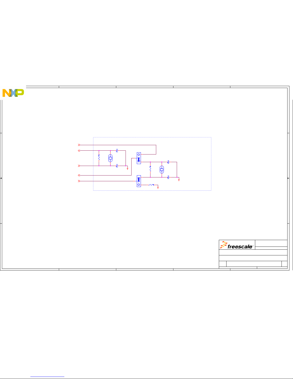
5
5
4
4
3
3
2
2
1
1
D D
C C
B B
A A
Oscillators and External Clock
(XTAL32)
(EXTAL32)
NX8045GB-40.000M-STD-CSJ-1 XTAL
(Optimised for Automotive, 8pF Load capacitance)
FC-255 32.7680K-A3
(Load Capacitance 7pF)
(From SMA connector on main board)
Clocks
EXTAL
MCU-XTAL
PB8
MCU-EXTAL
XTAL
PB9
EXT-CLK
GND
GND
GND
MCU-XTAL
4
PB8
4
PB94
MCU-EXTAL4
EXT-CLK
8
Drawing Title:
Size Document Number Rev
Date: Sheet
of
Page Title:
Automotive Microcontroller
Applications
East Kilbride, Scotland
SCH-27900 PDF: SPF-27900 A1
MPC5748G 324 BGA Daughter Card
B
Tuesday, August 18, 2015
Clocks
68
Freescale General Business Use
Drawing Title:
Size Document Number Rev
Date: Sheet of
Page Title:
Automotive Microcontroller
Applications
East Kilbride, Scotland
SCH-27900 PDF: SPF-27900 A1
MPC5748G 324 BGA Daughter Card
B
Tuesday, August 18, 2015
Clocks
68
Freescale General Business Use
Drawing Title:
Size Document Number Rev
Date: Sheet of
Page Title:
Automotive Microcontroller
Applications
East Kilbride, Scotland
SCH-27900 PDF: SPF-27900 A1
MPC5748G 324 BGA Daughter Card
B
Tuesday, August 18, 2015
Clocks
68
Freescale General Business Use
R33
1.0M
DNP
J2
1
2
3
Y20
32.768KHZ
1 2
C62 12PF
Y1
40.0MHZ
12
C7
12PF
C6
12PF
R34 0
DNP
C63
12PF
R8
1.0M
DNP
J1
1
2
3
Page 59
5
5
4
4
3
3
2
2
1
1
D D
C C
B B
A A
(PD[15] Shared with MLB_DAT for 3-pin mode)
(PB[15] Shared with MLB_SIG for 3-pin mode)
(PI[8] Shared with MLB_CLK for 3-pin mode)
Place resistors as close as possible to MCU
R1 Fitted by default
for LVDS 6-pin signals
Remove R1 and
fit R2 to
enable 3-pin
signals
Layout Note - Place resistors as shown with
shared pad (as close to MCU as possible)
Place resistors as close as possible to MCU
From MCU To Daughtercard
MLB Termination
Ethernet Termination
High Speed Signal Termination
PB14
PD15
PB13
PD14
PI8
MLB_SN
MLB_SP
MLB_DN
MLB_DP
MLB_CN
MLB_CP
PB15
MLB_CLK
MLB_SIG
MLB_DAT
PH2
PH1
PG12
PH0
PG13
PH2-R
PH1-R
PH0-R
PG13-R
PG12-R
PG0-RPG0
PI8
5
PB144
PD15
4
PB154
PB134
PD14
4
MLB_DAT
8
MLB_SIG
8
MLB_CLK
8
MLB_SN
8
MLB_SP
8
MLB_DN
8
MLB_DP
8
MLB_CN
8
MLB_CP
8
PG13
4
PG12
4
PH0
4
PH1
4
PH2
4
PG13-R
8
PG12-R
8
PH0-R
8
PH1-R
8
PH2-R
8
PG0-R
8
PG0
4
Drawing Title:
Size Document Number Rev
Date: Sheet
of
Page Title:
Automotive Microcontroller
Applications
East Kilbride, Scotland
SCH-27900 PDF: SPF-27900 A1
MPC5748G 324 BGA Daughter Card
B
Tuesday, August 18, 2015
High Speed Signal Termination
78
Freescale General Business Use
Drawing Title:
Size Document Number Rev
Date: Sheet of
Page Title:
Automotive Microcontroller
Applications
East Kilbride, Scotland
SCH-27900 PDF: SPF-27900 A1
MPC5748G 324 BGA Daughter Card
B
Tuesday, August 18, 2015
High Speed Signal Termination
78
Freescale General Business Use
Drawing Title:
Size Document Number Rev
Date: Sheet of
Page Title:
Automotive Microcontroller
Applications
East Kilbride, Scotland
SCH-27900 PDF: SPF-27900 A1
MPC5748G 324 BGA Daughter Card
B
Tuesday, August 18, 2015
High Speed Signal Termination
78
Freescale General Business Use
R20
100
DNP
R27 100 1%
R26
0
R28
0
R32
0
R31 105.0 1%
R25
100
DNP
R22 105.0 1%
R30
0
R2 50
R3 50
R21
0
R23
0
R5 50
R29
100
DNP
R4 50
R1 50
R6 50
Page 60
5
5
4
4
3
3
2
2
1
1
D D
C C
B B
A A
Daughter Card Connectors (Plugs)
Notes:
- there was no neat way to fit these connectors onto a B sized sheet so unfortunately the sheet size
has been increased to C so will need to be printed on larger paper.
- The Crystal Signals are NOT routed via the daughtercard connectors
- The Specific MCU power pins are not routed via the daughter card however the jumpered MCU supply
lines are brought up from the main board (see the top pins of the connector on the left)
- The connector schematic symbols have been horizontally mirrored so they match the main EVB connector.
This has no bearing on the PCB placement or footprint. Pin1 on the recepticle mates with pin 1 on the
plug.
(GND)
(GND) (GND)
(GND)
(GND)
(GND)
(GND)
(GND)
(GND)
(GND)
(GND)
(GND)
(GND)
(GND)
(GND)
(GND)
(GND)
(GND)
(GND)
(GND)
(GND)
(GND)
(GND)
(GND)
(GND)
(GND)(GND)
(GND)
(GND)
(GND)
(GND)
(GND)
(GND)
(GND)
(GND)
(GND)
(GND)
(GND)
(GND)
(GND)
(GND)
(GND)
(GND)
(GND)
(GND)
(GND)
(GND)
(GND)
(GND)
(GND)
(GND)
(GND)
(GND)
(GND)
Plug
(GND)
(GND)
(GND)
(GND)
(GND)
(GND)
(GND)
(GND)
(GND) (GND)
(GND)
(GND)
(GND)
(GND)
(GND)
(GND)
(GND)
(GND)
(GND)
(GND)
(GND)
(GND)
(GND)
(GND)
(GND)
(GND)
(GND)
(GND)
(GND)
(GND)
(GND)
(GND)
(GND)
(GND)
(GND)
(GND)
(GND)
(GND)
(GND)
(GND)
(GND)
(GND)(GND)
Connectors on Main board (Shown for reference)
Plug
PB3
PA12
PF0
PF1
PN2
PN5
PH8
PH7
PP8
PH6
PP3
PE7
PK9
PC12
PK11
PP4
PA13
PN4
PC8 PK14
PK13 PK12
PC9
PP2 PL0
PK15
PC15 PP1
PP7
PC14
PP6 PJ4
PO12
PO7
PO10
PJ14
PN7
PF10
PN8
PO4 PH14
PO9 PO13
PO1PG5
PH13PO14
PO0
PJ15
PG4
PI7 PH15
PP0 PO15
PE10
PE1 PE0
PI6 PO6
PO5
PE11 PG2
PC7
PN12
PJ12
PG3 PA2
PE9
PE8 PA1
MCU-RSTx
PF8
PK7
PC6
PG9 PN15
PF13
PK4
PK6
PA0 PO3
PN14
PK8
PG7 PG6
PG8 PC11
PC10 PO2
PB0
PB10
PN0
PN6
PN3
PA15
PN10
PA4
PJ13
PN9
PJ9
PB1 PK1
PK2 PF12
PK3
PK5
PF11
PF9
PA14
PN13
PN11
PJ11
PJ10
PK0
PE6
PI3
PP10
PP5
PI1
PI2
PP9
PC13
PI0
PK10
PB2
PP11
EXT-CLK
PO11
PO8
MCU_5V0_S
MCU_1V25_L
MCU_3V3_S
MCU_3V3_L
MCU_5V0_L
DC_5V0_S
DC_P12V
DC_1V25_L
DC_3V3_S
DC_5V0_L
DC_3V3_L
PF3
PF7
PF4
PL10
PE5
PG14
PM12
PQ0
PI5
PC5
PQ3
PE4
PC3
PC2
PL15
PM2
PM1
PC0
PA8
PH2-R
PG0-R
PF14
PA9
PA10
PA7
PG1
PF15
PE13
PA11
PE12
PL14
PM7
PM9
PL11 PL5
PH1-R
PH0-R
PA3
PG12-R
PG13-R
PH9
PI13
PM11
PM4
PL1
PM5
PM3
PM14
PC1
PM13
PH10
PB12
PE3
PH4 PH5
PL4
PE15
PL9
PL3
PH12
PG11
PG10
PL8
PORSTx
PH11
PE14
PG15
PC4
PQ1
PQ2
PQ6
PP13
PP12
PE2
PA6
PA5
PQ4
PQ5
PQ7 PI4
PP15 PP14
PF5
PI9
PD8
PJ3
PJ2
PB4
PM15
PF2
PD7
PJ5
PJ0
PD5
PB5
PJ1
PD1
PB11
MLB_DN
MLB_DP
PI10
PD0
PB6
PN1
PF6
PD4
PI14
PJ7
PD11
PJ6
PD6
PD2
PJ8
PD3
MLB_DAT
MLB_CP
MLB_CN
MLB_CLK
MLB_SIG
MLB_SN
MLB_SP
PL12 PL2
PL13PL6
PM0
PM10
PL7
PM8
PH3
PM6
PI11
PI12PD12
PD9PD13
PI15PD10
PB7
GND GND
GND GND
PN5
5
PA12
4
PN2
5
PF1
4
PF0
4
PN4
5
PA13
4
PN8
5
PF10
4
PN7
5
PJ14
5
PJ15
5
PC7
4
PN12
5
PJ12
5
PF8
4
PK7
5
PC6
4
PF13
4
PK4
5
PK6
5
PK8
5
PN14
5
PH7
4
PH6
4
PB3
4
PP8
5
PH8
4
PP3
5
PE7
4
PK9
5
PC12
4
PK11
5
PP4
5
PK14
5
PK12
5
PC9
4
PL0
5
PP1
5
PC14
4
PJ4
5
PH14
4
PO13
5
PO1
5
PH13
4
PG4
4
PH15
4
PO15
5
PE10
4
PE0
4
PO6
5
PG2
4
PA2
4
PE9
4
PA1
4
MCU-RSTx
4
PN15
5
PO3
5
PG6
4
PC11
4
PO2
5
PB0
4
PK1
5
PF12
4
PK3
5
PK5
5
PF11
4
PC8
4
PK13
5
PP2
5
PK15
5
PC15
4
PP7
5
PP6
5
PO12
5
PO7
5
PO10
5
PO4
5
PO9
5
PG5
4
PO14
5
PO0
5
PI75
PP0
5
PE1
4
PI6
5
PO5
5
PE11
4
PG3
4
PE8
4
PG9
4
PA0
4
PG7
4
PG8
4
PC10
4
PB1
4
PK2
5
PF9
4
PA14
4
PN13
5
PN11
5
PJ11
5
PJ10
5
PK0
5
PJ9
5
PN9
5
PJ13
5
PE6
4
PI3
5
PP10
5
PA4
4
PP5
5
PI1
5
PI2
5
PN10
5
PP9
5
PC13
4
PI0
5
PA15
4
PK10
5
PN3
5
PB2
4
PP11
5
PN6
5
PN0
5
PB10
4
EXT-CLK6
PO11
5
PO8
5
MCU_5V0_S
2
MCU_1V25_L
2
MCU_3V3_S
2
MCU_3V3_L
2
MCU_5V0_L
2
PF4
4
PF7
4
PF3
4
PL15
5
PM1
5
PM2
5
PC0
4
PL14
5
PM9
5
PM7
5
PH9
4
MLB_DN
7
MLB_DP
7
PC1
4
PE3
4
PH5
4
PQ3
5
PC3
4
PE4
4
PL10
5
PE15
4
PORSTx
4
PE2
4
PL4
5
PG11
4
PQ1
5
PG10
4
PQ2
5
PL8
5
PQ6
5
PP13
5
PP12
5
PI4
5
PP14
5
PL2
5
PL5
5
PL13
5
PM0
5
PA10
4
PA9
4
PA8
4
PF14
4
PG0-R
7
PH2-R
7
PG12-R
7
PG13-R
7
PM10
5
PM4
5
PL1
5
PM5
5
PI13
5
PB12
4
PD9
4
PI12
5
PB7
4
PI15
5
MLB_CN
7
MLB_CP
7
PI14
5
PJ7
5
PD11
4
PJ6
5
PD6
4
PD2
4
PD3
4
PJ8
5
PB6
4
PD0
4
PI10
5
PD4
4
PF6
4
PN1
5
PM11
5
PH10
4
PH4
4
PE5
4
PM12
5
PI5
5
PQ0
5
PC5
4
PG14
4
PH12
4
PC4
4
PL9
5
PC2
4
PA6
4
PL3
5
PH11
4
PA5
4
PE14
4
PQ4
5
PG15
4
PQ5
5
PQ7
5
PP15
5
PL12
5
PL11
5
PL6
5
PL7
5
PE12
4
PA11
4
PA7
4
PE13
4
PF15
4
PG1
4
PH1-R
7
PH0-R
7
PA3
4
PM8
5
PH3
4
PM3
5
PM6
5
PM13
5
PM14
5
PD13
4
PD12
4
PI11
5
PD10
4
MLB_DAT
7
MLB_SIG
7
MLB_CLK
7
MLB_SN
7
MLB_SP
7
PD7
4
PJ5
5
PJ0
5
PD5
4
PB5
4
PB11
4
PD1
4
PJ1
5
PD8
4
PI9
5
PF5
4
PB4
4
PJ2
5
PJ3
5
PF2
4
PM15
5
Drawing Title:
Size Document Number Rev
Date: Sheet
of
Page Title:
Automotive Microcontroller
Applications
East Kilbride, Scotland
SCH-27900 PDF: SPF-27900 A1
MPC5748G 324 BGA Daughter Card
C
Tuesday, August 18, 2015
Daughter Card Connectors (Plugs)
88
Freescale General Business Use
Drawing Title:
Size Document Number Rev
Date: Sheet of
Page Title:
Automotive Microcontroller
Applications
East Kilbride, Scotland
SCH-27900 PDF: SPF-27900 A1
MPC5748G 324 BGA Daughter Card
C
Tuesday, August 18, 2015
Daughter Card Connectors (Plugs)
88
Freescale General Business Use
Drawing Title:
Size Document Number Rev
Date: Sheet of
Page Title:
Automotive Microcontroller
Applications
East Kilbride, Scotland
SCH-27900 PDF: SPF-27900 A1
MPC5748G 324 BGA Daughter Card
C
Tuesday, August 18, 2015
Daughter Card Connectors (Plugs)
88
Freescale General Business Use
TPV1
TPV2 TPV6
TPV5
P21
PLUG 180
2
SH1SH2
SH5SH6
1
43
65
87
109
1211
1413
1615
1817
2019
2221
2423
2625
2827
3029
3231
3433
3635
3837
4039
4241
4443
4645
4847
5049
5251
5453
5655
5857
6059
SH3SH4
6261
6463
6665
6867
7069
7271
7473
7675
7877
8079
8281
8483
8685
8887
9089
9291
9493
9695
9897
10099
102101
104103
106105
108107
110109
112111
114113
116115
118117
120119
SH7SH8
SH9SH10
122121
124123
126125
128127
130129
132131
134133
136135
138137
140139
142141
144143
146145
148147
150149
152151
154153
156155
158157
160159
162161
164163
166165
168167
170169
172171
174173
176175
178177
180179
SH11SH12
TPV3
TPV4
P20
PLUG 180
2
SH1SH2
SH5SH6
1
43
65
87
109
1211
1413
1615
1817
2019
2221
2423
2625
2827
3029
3231
3433
3635
3837
4039
4241
4443
4645
4847
5049
5251
5453
5655
5857
6059
SH3SH4
6261
6463
6665
6867
7069
7271
7473
7675
7877
8079
8281
8483
8685
8887
9089
9291
9493
9695
9897
10099
102101
104103
106105
108107
110109
112111
114113
116115
118117
120119
SH7SH8
SH9SH10
122121
124123
126125
128127
130129
132131
134133
136135
138137
140139
142141
144143
146145
148147
150149
152151
154153
156155
158157
160159
162161
164163
166165
168167
170169
172171
174173
176175
178177
180179
SH11SH12
Page 61

256 BGA DC
Page 62
5
5
4
4
3
3
2
2
1
1
D D
C C
B B
A A
Freescale AISG Applications, East Kilbride
A
X2
X3
X4
Revision Information
Designer CommentsRev Date
GPIO - MPC5748G GPIO pins 1 of 2
Clocks
Sheet 8
Sheet 2
Sheet 3
Sheet 4
Sheet 5
Sheet 6
Sheet 7
GPIO - MPC5748G GPIO pins 2 of 2
Table Of Contents:
MPC5748G Customer EVB 256BGA [6M/3M] Daughter Card (X-MPC574XG-256DS)
X1
Power - MPC5748G power pins footprint
Power - MPC5748G Decoupling Capacitors
Daughtercard Connectors
Bus Termination
11 Mar 2013 Alasdair Robertson Initial release sent for review based on X-MPC574XG-324DS X2
These schematics are provided for reference purposes only. As such,
Freescale does not make any warranty, implied or otherwise, as to the
suitability of circuit design or component selection (type or value) used in
these schematics for hardware design using the Freescale MPC5748G family
of Microprocessors. Customers using any part of these schematics as a
basis for hardware design, do so at their own risk and Freescale does not
assume any liability for such a hardware design.
User notes are given throughtout the schematics.
Specific PCB LAYOUT notes are detailed in ITALICS
Caution:
Notes:
- All components and board processes are to be ROHS compliant
- All small capacitors are 0402 unless otherwise stated
- All resistors are 0603 5% 0.1w unless otherwise stated. All zero ohm links are 0603
- All connectors and headers are denoted Px and are 2.54mm pitch unless otherwise stated
- All jumpers are denoted Jx. Jumpers are 2mm pitch
- Jumper default positions are shown in the schematics. For 3 way jumpers, default is always posn 1-2.
2 Pin jumpers generally have the "source" on pin 1.
- All switches are denoted SWx
- All test points are denoted TPx
- Test point Vias are denoted TPVx
13 Mar 2013 Alasdair Robertson
15 Mar 2013 Component consolodation, Few minor changes. Sent to LayoutAlasdair Robertson
Version sent to Pre Layout, incorporating fixes from review
29 Mar 2013 Alasdair Robertson Changes made during layout to Daughtercard Connectors
Alasdair Robertson Post Layout (Back Annotated). Matches PCB RevA
15 Apr 2013 Alasdair Robertson LAY RefDes Re-Sequence & SCH Back-AnnotateX5
15 Apr 2013
Changes on MCU Power to validate MPC5746Jesus Sanchez16 Mar 2014X1
SCH-27899 change to SCH-28341
A 18 Apr 2014 Jesus Sanchez Post Layout. RevA.
A1 Alasdair Robertson Tidy up Schematics for UM (RevA PCB)18 Aug 2015
Drawing Title:
Size Document Number Rev
Date: Sheet
of
Page Title:
Designer:
Drawn by:
Approved:
Automotive Microcontroller Applications
East Kilbride, Scotland
This document contains information proprietary to Freescale and shall not be used for engineering design,
procurement or manufacture in whole or in part without the express written permission of Freescale
SCH-28341 PDF: SPF-28341 A
MPC5748G 256 BGA Daughter Card
B
Tuesday, August 18, 2015
Index and Title Page
A. Robertson / J. Sanchez
A. Robertson / J. Sanchez
A. Robertson
18
Freescale General Business Use
Drawing Title:
Size Document Number Rev
Date: Sheet
of
Page Title:
Designer:
Drawn by:
Approved:
Automotive Microcontroller Applications
East Kilbride, Scotland
This document contains information proprietary to Freescale and shall not be used for engineering design,
procurement or manufacture in whole or in part without the express written permission of Freescale
SCH-28341 PDF: SPF-28341 A
MPC5748G 256 BGA Daughter Card
B
Tuesday, August 18, 2015
Index and Title Page
A. Robertson / J. Sanchez
A. Robertson / J. Sanchez
A. Robertson
18
Freescale General Business Use
Drawing Title:
Size Document Number Rev
Date: Sheet
of
Page Title:
Designer:
Drawn by:
Approved:
Automotive Microcontroller Applications
East Kilbride, Scotland
This document contains information proprietary to Freescale and shall not be used for engineering design,
procurement or manufacture in whole or in part without the express written permission of Freescale
SCH-28341 PDF: SPF-28341 A
MPC5748G 256 BGA Daughter Card
B
Tuesday, August 18, 2015
Index and Title Page
A. Robertson / J. Sanchez
A. Robertson / J. Sanchez
A. Robertson
18
Freescale General Business Use
Page 63
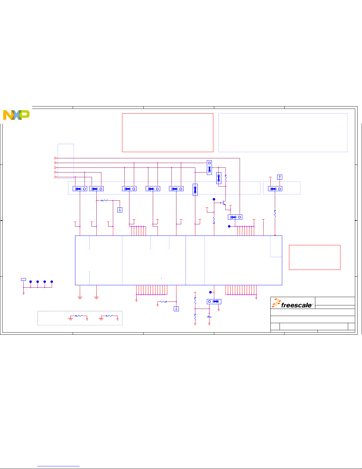
5
5
4
4
3
3
2
2
1
1
D D
C C
B B
A A
Individual MCU
supply control
jumpers
3v3
Default Configuraiton:
- ALL MCU supply voltages are set to 3.3V (ADC0, ADC1, VDD_HV_A,
VDD_HV_B, VDD_HV_C, VBallast)
- VDD_HV_FLA = External 3.3V supplied (jumper fitted)
- VDD_LV Supplied from ballast transistor
This is not necessarily the same as the default shown in the RM. All
VDD_HV_x domains have at least one peripheral that only functions at
3.3V. Therefore the default is to run these from 3.3V. The analogue pins
can only be driven to the same voltage as the VDD_HV_x domain they are
situated in (ie max 3.3V) so makes sense for the analogue supply and
reference to be 3.3V
Ground Links
(0 Ohm
Resistors)
DAC External
Ref Voltage
Select
3v3 5v0 5v0 5v0 5v0 5v03v3 3v3 3v3
3v3
3v3
5v0
(Current Limit Resistor to
protecxt against case when
other MCU supplies are
disconnected and external
reference supply is live)
MPC5748G MCU Power Connections
Caution:
- If VDD_HV_A is driven from 5V, the VDD_HV_FLA pin
must not be supplied from 3.3V (remove the HVA_FLA
jumper)
- Don't attempt to over drive an analogue pad to 5V
when the digital VDD_HV_x supply is set to 3.3V. This
will trigger the ESD protectrion on that pad. For
example if VDD_HV_A is set to 3.3V and the analogue
supplies are set to 5V, you cannot drive 5V into a
pad in the VDD_HV_A domain
Differences to 324BGA
- 1 more VDD_HV_A on 256BGA
- 1 fewer VDD_HV_B
- 1 fewer VDD_LV
- 2 more VSS_HV
- 1 fewer VSS_LV
From MCU
supply
jumpers on
main board
MCU_3V3_S
MCU_5V0_S
MCU_1V25_L
MCU_3V3_L
MCU_5V0_L
HVB_CAP
HVC_CAP
HVFLA_CAP
LV_CAP
ADC0_CAP
ADC1_CAP
ADC1REF_CAP
ADC0_GND ADC1_GND GND
HVA_CAP
GNDADC0_GND GNDADC1_GND
E_CAP
B_CAP
LVDEC_CAP
HVA_CAP
GND
GND
HVA_CAP
GND
GND
GND
GND
MCU_1V25_L8
MCU_5V0_S8
MCU_3V3_S8
MCU_5V0_L8
MCU_3V3_L8
Drawing Title:
Size Document Number Rev
Date: Sheet
of
Page Title:
Automotive Microcontroller
Applications
East Kilbride, Scotland
SCH-28341 PDF: SPF-28341 A
MPC5748G 256 BGA Daughter Card
B
Tuesday, August 18, 2015
MPC5748G MCU Power
28
Freescale General Business Use
Drawing Title:
Size Document Number Rev
Date: Sheet of
Page Title:
Automotive Microcontroller
Applications
East Kilbride, Scotland
SCH-28341 PDF: SPF-28341 A
MPC5748G 256 BGA Daughter Card
B
Tuesday, August 18, 2015
MPC5748G MCU Power
28
Freescale General Business Use
Drawing Title:
Size Document Number Rev
Date: Sheet of
Page Title:
Automotive Microcontroller
Applications
East Kilbride, Scotland
SCH-28341 PDF: SPF-28341 A
MPC5748G 256 BGA Daughter Card
B
Tuesday, August 18, 2015
MPC5748G MCU Power
28
Freescale General Business Use
TP12
TP10
1
C63
1.0 UF
DNP
J11
123
J12
12
R37
1.0
DNP
TP11
Q20
MJD31CT4
3 4
1
J3
123
R39
10K
DNP
J10
123
TP2
R10
0
R36
1.0K
1.25v Core & External BallastAnalogue
MPC5748G 256 BGA
Package 2of3 Power Pins
Flash
DAC Ref
U1B
PPC5748GSK0MMJ6 + OTB-256(324R)-1.0-006-00
VRC_CTRL
J2
VSS_LV_E6E6VSS_LV_H6H6VSS_LV_H7H7VSS_LV_H15
H15
VSS_LV_J6J6VSS_LV_J7J7VSS_LV_J8J8VSS_LV_K6K6VSS_LV_K7K7VSS_LV_K8K8VSS_LV_K9
K9
VSS_LV_L6
L6
VSS_LV_L7L7VSS_LV_L8L8VSS_LV_L9
L9
VDD_LV_D8
D8
VDD_LV_E5
E5
VDD_LV_H14
H14
VDD_LV_J3
J3
VDD_LV_K10
K10
VDD_LV_K11
K11
VDD_LV_L10
L10
VDD_LV_L11
L11
VDD_HV_A_C2C2VDD_HV_A_C9C9VDD_HV_A_N6
N6
VDD_HV_A_E16
E16
VDD_HV_A_H13
H13
VDD_HV_A_N9
N9
VDD_HV_B_G13
G13
VDD_HV_C_M10
M10
VSS_HV_ADC0
T15
VDD_HV_ADC0
R15
VDD_HV_ADC1
L16
VSS_HV_ADC1
M16
VDD_HV_FLA_H2
H2
VDD_HV_ADC1_REF
M11
VSS_HV_G6G6VSS_HV_G7G7VSS_HV_G8G8VSS_HV_G9G9VSS_HV_G10
G10
VSS_HV_G11
G11
VSS_HV_H8H8VSS_HV_H9H9VSS_HV_H10
H10
VSS_HV_H11
H11
VSS_HV_J9J9VSS_HV_J10
J10
VIN1_CMP_REF
M9
VDD_LP_DEC
K2
VSS_HV_VPP
J1
VDD_HV_A_R9
R9
VSS_HV_J11
J11
VSS_HV_T9
T9
TP1
J7
123
TPH2
1
J5
123
R38
10K
TPH3
1
TPH1
1
J13
123
J6
123
J4
123
R9
0
TP3
R7
0
J8
12
R35
0
J9
1
2
3
TP14TP13
R24
0
Page 64
5
5
4
4
3
3
2
2
1
1
D D
C C
B B
A A
Capacitor Types:
470pF - Ceramic COG, 50v 5% 0402
1000pF - Ceramic COG, 50V 5% 0402
4700pF - Ceramic X7R, 50V 10% 0402
0.01uF - Ceramic X7R, 50V 10% 0402
0.1uF - Ceramic X7R, 16V 10% 0402
0.68uF - Ceramic X7R 16V 10% 0805 (Murata GCM219R71C684KA37 )
1.0uF - Ceraminc X7R, 10V 10% 0603 (Taiyo Yuden LMK107B7105KA-T)
2.2uF - Ceraminc X7R, 10V, 10%, 0603 (Taiyo Yuden LMK107B7225KA-TR)
4.7uF - TANT, 12.5V 20% ESR=0.08R 7343
10uF - TANT, 35V 10% ESR=0.125R CC7343-31
4.7uF Alternative (150-78844)- Polymer ALU, 16V 20% ESR=0.08R
7343-18
Place small Caps as close as possible to MCU pins
ADC
Place small caps close to each MCU pin
VDD_HVA VDD_HVB VDD_HVC
VDD_LV
See caps below for Bypass Transistor bulk storage (some on VDD1V2 rail)
VDD_LV (1.25V) Decoupling. Place one of the non DNP caps each side of the device
as close as possible to pin. Distribute other (DNP) caps around rest of pins
Ballast Transistor
Flash
MPC5748G MCU Decoupling and bulk storage
LP Internal Reg Cap
Place
close to
transistor
Place one 0.68uF cap footprint
each side of package
Place 10uF cap to west side of package
(low ESR)
(low
ESR)
(low
ESR)
(Murata GCM219R71C684KA37)
(low
ESR)
(low
ESR)
(low
ESR)
(low
ESR)
(low ESR)
2.2uF caps
are DNP.
Place close
to emitter
One of these is DNP. May replace 2 caps with
0.47uF to keep overall capacitance within limits
Differences to 324BGA
- 1 more VDD_HV_A capacitor pair
- 1 fewer VDD_HV_B capacitor pair
- 1 fewer VDD_LV capacitor (one of DNP caps)
ADC0_CAP
ADC0_GND
ADC1REF_CAP
ADC1_GND
ADC1_CAP
ADC1_GND
GND
HVA_CAP
GND
HVB_CAP
GND
HVC_CAP
LV_CAP
GND
HVFLA_CAP
GND
LV_CAPB_CAP E_CAP
GND
LVDEC_CAP
GND
E_CAP
GND
Drawing Title:
Size Document Number Rev
Date: Sheet
of
Page Title:
Automotive Microcontroller
Applications
East Kilbride, Scotland
SCH-28341 PDF: SPF-28341 A
MPC5748G 256 BGA Daughter Card
B
Tuesday, August 18, 2015
MPC5748G MCU Decoupling
38
Freescale General Business Use
Drawing Title:
Size Document Number Rev
Date: Sheet of
Page Title:
Automotive Microcontroller
Applications
East Kilbride, Scotland
SCH-28341 PDF: SPF-28341 A
MPC5748G 256 BGA Daughter Card
B
Tuesday, August 18, 2015
MPC5748G MCU Decoupling
38
Freescale General Business Use
Drawing Title:
Size Document Number Rev
Date: Sheet of
Page Title:
Automotive Microcontroller
Applications
East Kilbride, Scotland
SCH-28341 PDF: SPF-28341 A
MPC5748G 256 BGA Daughter Card
B
Tuesday, August 18, 2015
MPC5748G MCU Decoupling
38
Freescale General Business Use
C30
0.1UF
C42
1000pF
C26
0.1UF
C50
0.1UF
DNP
C24
0.1UF
C33
470pF
C60
0.68uF
C47
1000pF
C44
0.1UF
C58
1.0 UF
C49
0.1UF
C34
2.2UF
LMK107B7225KA-T
C32
0.1UF
C43
1uF
LMK107B7105KA-T
C25
0.1UF
DNP
C29
0.68uF
C41
0.1UF
C52
0.1UF
C28
470pF
C10
2.2UF
DNP
C51
1000pF
C56
0.1UF
C20
0.68uF
DNP
C23
0.1UF
C48
1000pF
+
C4
10UF
DNP
C39
0.1UF
C55
0.1UF
C57
1.0 UF
C54
1000pF
C9
2.2UF
DNP
C46
1000pF
C36
1000pF
C53
0.1UF
+
C1
10UF
+
C2
10UF
DNP
C38
0.1UF
C8 4700pF
C59
1.0 UF
C40
470pF
C21
0.1UF
DNP
C27
470pF
C31
0.68uF
C35
0.1UF
+
C3
10UF
DNP
C45
0.1UF
DNP
C37
1000pF
+
C5
10UF
DNP
C22
470pF
Page 65
5
5
4
4
3
3
2
2
1
1
D D
C C
B B
A A
MPC5748G GPIO 1 of 2
Key to text colours:
Purple - Comms Physical Interfaces
Blue - Debug (JTAG & Nexus)
(LIN0_RX)
(LIN0_TX)
(LIN1_TX)
(LIN1_RX)
(XTAL32)
(EXTAL32)
(FR_A_TX)
(FR_A_TX_EN)
(FR_A_RX)
(FR_B_TX_EN)
(FR_B_RX)
(FR_B_TX)
(USB1_CLK)
(USB1_D0)
(USB1_D1)
(USB1_D2)
(USB1_D3)
(USB1_D4)
(USB1_D5)
(USB1_D6)
(USB1_D7)
(USB1_DIR)
Orange - Other Peripherals and I/O
(RMII_RXD0)
(RMII_RXD1)
(MII_RXD2)
(MII_RXD3)
(MII_CRS)
(RMII_TXD0)
(RMII_TXD1)
(MII_TXD2)
(MII_TXD3)
(RMII_TXEN)
(RMII_MDC)
(RMII_TXCLK)
(RMII_RXDV)
(RMII_MDIO)
(RMII_RXER)
(MII_COL)
(MII_RXCLK)
(FR_DBG0)
(FR_DBG1)
(FR_DBG2)
(FR_DBG3)
(SD_CMD)
(SD_CLK)
(SD_WP)
(SAI0_D0)
(SAI0_D1)
(SAI0_D2)
(SAI0_D3)
(SAI0_BCLK)
(SAI0_MCLK)
(SAI0_SYNC)
(SAI1_SYNC)
(SAI1_MCLK)
(TDI)
(TDO)
(TCK)
(TMS)
Black - Clock, Reset and Control
(MLB_DN)
(MLB_DP)
(MLB_SN)
(MLB_SP / DAT)
(MLB_CN / SIG)
(SAI_I2C2_SCL)
(SAI_I2C2_SDA)
(SAI_I2C3_SDA)
(SAI_I2C3_SCL)
(MLB_I2C1_SCL)
(MLB_I2C1_SDA)
Green - I/O Matrix (dedicated)
(CMP1_8 / IO)
(CMP1_10 / IO)
(CMP1_11 /IO)
(CMP1_12 / IO)
(CMP1_13 / IO)
(CMP1_14 / IO)
(CMP1_15 / IO)
(CLKOUT1 GPIO)
(GPIO)
(GPIO)
(HEX1 & GPIO)
(HEX2 & GPIO)
(HEX3 & GPIO)
(HEX4 & GPIO)
(SW1 & GPIO**)
(SW2 & GPIO)
(LED1 & GPIO)
(LED2 & GPIO)
(LED3 & GPIO)
(LED4 & GPIO)
(MLB_RST)
(MLB_PWR)
(MLB_IRQ - WKPU21)
** PA1 is also NMI. Routed to I/O Matrix
RED - I/O Matrix and other functions (eg LED)
(CLKOUT0 GPIO)
(eMIOS1_UC_5H)
(eMIOS1_UC_6H)
(eMIOS1_UC_7H)
(ADC_POT)
(GPIO)
(GPIO)
(GPIO)
(GPIO)
(GPIO)
(GPIO)
(GPIO)
(GPIO)
(GPIO)
(GPIO)
(GPIO)
(GPIO)
(GPIO)
(GPIO)
(GPIO)
(CAN0_TX)
(CAN0_RX)
(SW4 & GPIO)
(CAN1_RX)
(CAN1_TX)
(SW3 & GPIO)
(RS232_RX)
(RS232_TX)
(SD_CD - WKPU19)
(GPIO)
(GPIO)
(GPIO)
(eMIOS E1UC_11_H)
(eMIOS E1UC_12_H)
(eMIOS E1UC_13_H)
(eMIOS E1UC_14_H)
(WKPU2 / NMI0)
(WKPU3)
WKPU22
WKPU15
Differences to 324BGA
(none on this page)
(SAI_GPIO)
(MLB_GPIO)
(GPIO & MLB_ST)
PA0
PA1
PA3
PA2
PA4
PB3
PB4
PC3
PC4
PD3
PD4
PE0
PE1
PE3
PE2
PE4
PE5
PE7
PE6
PE8
PE9
PE11
PE10
PE12
PE13
PE15
PE14
PF0
PF1
PF3
PF2
PF4
PF5
PF7
PF6
PF8
PF9
PF11
PF10
PF12
PF13
PF15
PF14
PG0
PG1
PG3
PG2
PG4
PG5
PG7
PG6
PG8
PG9
PG11
PG10
PG12
PG13
PG15
PG14
PH0
PH1
PH3
PH2
PH4
PH5
PH7
PH6
PH8
PH9
PH11
PH10
PH12
PH13
PH15
PH14
MCU-EXTAL
PA5
PA7
PA8
PA6
PA10
PA13
PA12
PA11
PA9
PA14
PA15
PB1
PB0
PB8
PB11
PB10
PB9
PB2
PB5
PB7
PB6
PB12
PB14
PB13
PB15
PC0
PD6
PC12
PC14
PC15
PC9
PD8
PC5
PC10
PD2
PC11
PD0
PC6
PC7
PC1
PD7
PD5
PC8
PD11
PD9
PC13
PC2
PD1
PD10
PD14
PD15
PD13
PD12
MCU-RSTx
PORSTx
MCU-XTAL
PH0
7
PORSTx
8
MCU-RSTx8
MCU-EXTAL
6
MCU-XTAL6
PB08
PB18
PB28
PB38
PB118
PB128
PB137
PB147
PB157
PB68
PB78
PB86
PB96
PB108
PA118
PA128
PA138
PA148
PA158
PA68
PA78
PA88
PA98
PA108
PA58
PA08
PA18
PA28
PA38
PA48
PB58
PB48
PC118
PC128
PC138
PC148
PC158
PC68
PC78
PC88
PC98
PC108
PC58
PC48
PC08
PC18
PC28
PC38
PD118
PD128
PD138
PD147
PD157
PD68
PD78
PD88
PD98
PD108
PD58
PD48
PD08
PD18
PD28
PD38
PH1
7
PH2
7
PH3
8
PH4
8
PH5
8
PH6
8
PH7
8
PH8
8
PH9
8
PH10
8
PH11
8
PH12
8
PH13
8
PH14
8
PH15
8
PG0
7
PG1
8
PG2
8
PG3
8
PG4
8
PG5
8
PG6
8
PG7
8
PG8
8
PG9
8
PG10
8
PG11
8
PG12
7
PG13
7
PG14
8
PG15
8
PF0
8
PF1
8
PF2
8
PF3
8
PF4
8
PF5
8
PF6
8
PF7
8
PF8
8
PF9
8
PF10
8
PF11
8
PF12
8
PF13
8
PF14
8
PF15
8
PE0
8
PE1
8
PE2
8
PE3
8
PE4
8
PE5
8
PE6
8
PE7
8
PE8
8
PE9
8
PE10
8
PE11
8
PE12
8
PE13
8
PE14
8
PE15
8
Drawing Title:
Size Document Number Rev
Date: Sheet
of
Page Title:
Automotive Microcontroller
Applications
East Kilbride, Scotland
SCH-28341 PDF: SPF-28341 A
MPC5748G 256 BGA Daughter Card
B
Tuesday, August 18, 2015
MPC5748G GPIO 1of2
48
Freescale General Business Use
Drawing Title:
Size Document Number Rev
Date: Sheet of
Page Title:
Automotive Microcontroller
Applications
East Kilbride, Scotland
SCH-28341 PDF: SPF-28341 A
MPC5748G 256 BGA Daughter Card
B
Tuesday, August 18, 2015
MPC5748G GPIO 1of2
48
Freescale General Business Use
Drawing Title:
Size Document Number Rev
Date: Sheet of
Page Title:
Automotive Microcontroller
Applications
East Kilbride, Scotland
SCH-28341 PDF: SPF-28341 A
MPC5748G 256 BGA Daughter Card
B
Tuesday, August 18, 2015
MPC5748G GPIO 1of2
48
Freescale General Business Use
MPC5748G 256 BGA
Package 1of3 GPIO Pins1
U1A
PPC5748GSK0MMJ6 + OTB-256(324R)-1.0-006-00
RESET
K1
PORST
C8
XTAL
T7
EXTAL
T8
PA0
G4
PA1
F3
PA2
F1
PA3
G16
PA4
T2
PA5
C10
PA6
D11
PA7
C15
PA8
B16
PA9
B15
PA10
A15
PA11
B14
PA12
P6
PA13
R5
PA14
P4
PA15
R2
PB0
L3
PB1
M2
PB2
A2
PB3
D4
PB4
T16
PB5
N13
PB6
N14
PB7
R16
PB8
T11
PB9
T10
PB10
N7
PB11
M13
PB12
L14
PB13
L15
PB14
K15
PB15
K16
PC0
B10
PC1
D9
PC2
B11
PC3
C11
PC4
A9
PC5
B9
PC6
N3
PC7
N4
PC8
B3
PC9
C3
PC10
L1
PC11
K4
PC12
B4
PC13
A3
PC14
B2
PC15
A1
PD0
R12
PD1
T13
PD2
N11
PD3
R13
PD4
P12
PD5
T14
PD6
R14
PD7
P13
PD8
P14
PD9
N16
PD10
M14
PD11
M15
PD12
L13
PD13
K14
PD14
K13
PD15
J13
PE0
G2
PE1
F4
PE2
A7
PE3
A10
PE4
A8
PE5
B8
PE6
B6
PE7
A5
PE8
G1
PE9
H1
PE10
G3
PE11
H3
PE12
C14
PE13
C16
PE14
A14
PE15
C12
PF0
P7
PF1
T6
PF2
R6
PF3
R7
PF4
R8
PF5
P8
PF6
N8
PF7
P9
PF8
N2
PF9
M4
PF10
P2
PF11
R1
PF12
P1
PF13
P3
PF14
D14
PF15
D15
PG0
E13
PG1
E14
PG2
E4
PG3
E1
PG4
F2
PG5
D1
PG6
M1
PG7
L2
PG8
K3
PG9
J4
PG10
B13
PG11
A16
PG12
F15
PG13
F16
PG14
C13
PG15
D13
PH0
E15
PH1
F13
PH2
D16
PH3
F14
PH4
D7
PH5
B7
PH6
C7
PH7
C6
PH8
A6
PH9
A11
PH10
D10
PH11
A13
PH12
B12
PH13
B1
PH14
C1
PH15
E3
Page 66
5
5
4
4
3
3
2
2
1
1
D D
C C
B B
A A
MPC5748G GPIO 2 of 2
(USB1_NXT)
(USB1_STP)
(USB0_CLK)
(USB0_D0)
(USB0_D1)
(USB0_D2)
(USB0_D3)
(USB0_D4)
(USB0_D5)
(USB0_D6)
(USB0_D7)
(USB0_NXT)
(USB0_DIR)
(USB0_STP)
(SD_D3)
(SD_D2)
(SD_D1)
(SD_D0)
(SAI1_D0)
(SAI1_BCLK)
(SAI2_D0)
(SAI2_BCLK)
(SAI2_MCLK)
(SAI2_SYNC)
(MLB_CP / CLK)
(GPIO)
(GPIO)
(GPIO)
(GPIO)
(GPIO)
(GPIO)
(GPIO)
(GPIO)
(GPIO)
(GPIO)
(GPIO)
(GPIO)
(GPIO)
(GPIO)
(GPIO)
(GPIO)
(GPIO)
(GPIO)
(GPIO)
(GPIO)
(GPIO)
(GPIO)
(GPIO)
(GPIO)
(GPIO)
(GPIO)
(GPIO)
(GPIO)
(GPIO)
(GPIO)
(GPIO)
(GPIO)
(GPIO)
(GPIO)
(GPIO)
(GPIO)
(GPIO)
(GPIO)
(GPIO)
(USB1_RST)
(USB0_RST)
(ENET_RST)
Green - I/O Matrix (dedicated)
Key to text colours:
Purple - Comms Physical Interfaces
Blue - Debug (JTAG & Nexus)
RED - I/O Matrix and other functions (eg LED)
Orange - Other Peripherals and I/O
Black - Clock, Reset and Control
Differences to 324BGA
- 14 fewer pins on Port L
- 12 fewer pins on Port M
- 16 fewer pins on Port N
- 14 fewer pins on Port O
- 12 fewer pins on Port P
(And corresponding changes
to daughtercard connectors)
(GPIO & MLB_PS0)
(GPIO & MLB_PS1)
PI0
PI1
PI3
PI2
PI4
PI5
PI7
PI6
PI8
PI9
PI11
PI10
PI12
PI13
PI15
PI14
PJ0
PJ1
PJ3
PJ2
PJ4
PJ7
PJ6
PJ8
PJ9
PJ11
PJ10
PJ12
PJ13
PJ15
PJ14
PK0
PK1
PK3
PK2
PK4
PK5
PK7
PK6
PK8
PK9
PK11
PK10
PK12
PK13
PK14
PL0
PL1
PM3
PM4
PM5
PM14
PO0
PO1
PP12
PP13
PP15
PP14
PK15
PQ1
PQ3
PQ2
PQ4
PQ5
PQ6
PJ5
PQ7
PQ0
PI118
PI128
PI138
PI148
PI158
PI68
PI78
PI87
PI98
PI108
PI58
PI08
PI18
PI28
PI38
PI48
PJ118
PJ128
PJ138
PJ148
PJ158
PJ68
PJ78
PJ88
PJ98
PJ108
PJ58
PJ08
PJ18
PJ28
PJ38
PJ48
PK118
PK128
PK138
PK148
PK158
PK68
PK78
PK88
PK98
PK108
PK58
PK08
PK18
PK28
PK38
PK48
PL08
PL18
PM3
8
PM4
8
PM5
8
PM14
8
PO0
8
PO1
8
PP12
8
PP13
8
PP14
8
PP15
8
PQ48
PQ58
PQ68
PQ78
PQ08
PQ18
PQ28
PQ38
Drawing Title:
Size Document Number Rev
Date: Sheet
of
Page Title:
Automotive Microcontroller
Applications
East Kilbride, Scotland
SCH-28341 PDF: SPF-28341 A
MPC5748G 256 BGA Daughter Card
B
Tuesday, August 18, 2015
MPC5748G GPIO 2of2
58
Freescale General Business Use
Drawing Title:
Size Document Number Rev
Date: Sheet of
Page Title:
Automotive Microcontroller
Applications
East Kilbride, Scotland
SCH-28341 PDF: SPF-28341 A
MPC5748G 256 BGA Daughter Card
B
Tuesday, August 18, 2015
MPC5748G GPIO 2of2
58
Freescale General Business Use
Drawing Title:
Size Document Number Rev
Date: Sheet of
Page Title:
Automotive Microcontroller
Applications
East Kilbride, Scotland
SCH-28341 PDF: SPF-28341 A
MPC5748G 256 BGA Daughter Card
B
Tuesday, August 18, 2015
MPC5748G GPIO 2of2
58
Freescale General Business Use
MPC5748G 256 BGA
Package 3of3 GPIO Pins2
U1C
PPC5748GSK0MMJ6 + OTB-256(324R)-1.0-006-00
PI0
C5
PI1
A4
PI2
D6
PI3
B5
PI4
A12
PI5
D12
PI6
D2
PI7
E2
PI8
J14
PI9
J15
PI10
J16
PI11
H16
PI12
G15
PI13
G14
PI14
T12
PI15
P11
PJ0
R11
PJ1
N10
PJ2
R10
PJ3
P10
PJ4
D3
PJ5
N12
PJ6
N15
PJ7
P16
PJ8
P15
PJ9
P5
PJ10
T5
PJ11
R3
PJ12
T1
PJ13
N5
PJ14
T4
PJ15
R4
PK0
T3
PK1
H4
PK2
L4
PK3
N1
PK4
M3
PK5
M5
PK6
M6
PK7
M7
PK8
M8
PK9
E8
PK10
E7
PK11
F8
PK12
G12
PK13
H12
PK14
J12
PK15
D5
PL0
C4
PL1
F7
PM3
K12
PM4
L12
PM5
F9
PM14
M12
PO0
K5
PO1
L5
PP12
E12
PP13
F12
PP14
E11
PP15
F11
PQ0
J5
PQ1
H5
PQ2
G5
PQ3
F5
PQ4
F6
PQ5
E9
PQ6
F10
PQ7
E10
Page 67
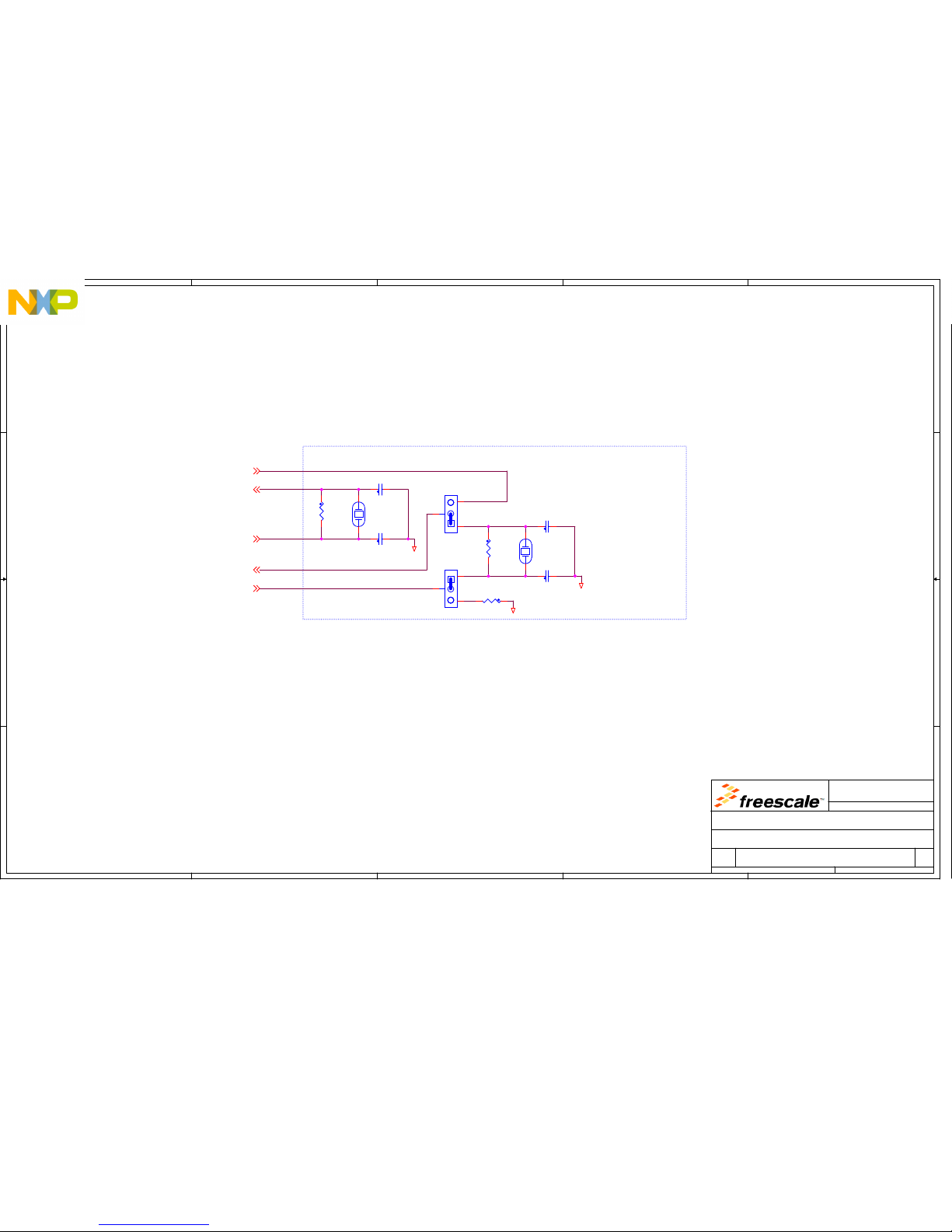
5
5
4
4
3
3
2
2
1
1
D D
C C
B B
A A
Oscillators and External Clock
(XTAL32)
(EXTAL32)
NX8045GB-40.000M-STD-CSJ-1 XTAL
(Optimised for Automotive, 8pF Load capacitance)
FC-255 32.7680K-A3
(Load Capacitance 7pF)
(From SMA connector on main board)
Clocks
EXTAL
MCU-XTAL
PB8
MCU-EXTAL
XTAL
PB9
EXT-CLK
GND
GND
GND
MCU-XTAL
4
PB8
4
PB94
MCU-EXTAL4
EXT-CLK
8
Drawing Title:
Size Document Number Rev
Date: Sheet
of
Page Title:
Automotive Microcontroller
Applications
East Kilbride, Scotland
SCH-28341 PDF: SPF-28341 A
MPC5748G 256 BGA Daughter Card
B
Tuesday, August 18, 2015
Clocks
68
Freescale General Business Use
Drawing Title:
Size Document Number Rev
Date: Sheet of
Page Title:
Automotive Microcontroller
Applications
East Kilbride, Scotland
SCH-28341 PDF: SPF-28341 A
MPC5748G 256 BGA Daughter Card
B
Tuesday, August 18, 2015
Clocks
68
Freescale General Business Use
Drawing Title:
Size Document Number Rev
Date: Sheet of
Page Title:
Automotive Microcontroller
Applications
East Kilbride, Scotland
SCH-28341 PDF: SPF-28341 A
MPC5748G 256 BGA Daughter Card
B
Tuesday, August 18, 2015
Clocks
68
Freescale General Business Use
J2
1
2
3
R8
1.0M
DNP
C61 12PF
Y20
32.768KHZ
1 2
C7
12PF
Y1
40.0MHZ
12
R33
1.0M
DNP
R34 0
DNP
C6
12PF
C62
12PF
J1
1
2
3
Page 68
5
5
4
4
3
3
2
2
1
1
D D
C C
B B
A A
(PD[15] Shared with MLB_DAT for 3-pin mode)
(PB[15] Shared with MLB_SIG for 3-pin mode)
(PI[8] Shared with MLB_CLK for 3-pin mode)
Place resistors as close as possible to MCU
R1 Fitted by default
for LVDS 6-pin signals
Remove R1 and
fit R2 to
enable 3-pin
signals
Layout Note - Place resistors as shown with
shared pad (as close to MCU as possible)
Place resistors as close as possible to MCU
From MCU To Daughtercard
MLB Termination
Ethernet Termination
High Speed Signal Termination
PB14
PD15
PB13
PD14
PI8
MLB_SN
MLB_SP
MLB_DN
MLB_DP
MLB_CN
MLB_CP
PB15
MLB_CLK
MLB_SIG
MLB_DAT
PH2
PH1
PG12
PH0
PG13
PH2-R
PH1-R
PH0-R
PG13-R
PG12-R
PG0-RPG0
PI8
5
PB144
PB154
PB134
MLB_DAT
8
MLB_SIG
8
MLB_CLK
8
MLB_SN
8
MLB_SP
8
MLB_DN
8
MLB_DP
8
MLB_CN
8
MLB_CP
8
PG13
4
PG12
4
PH0
4
PH1
4
PH2
4
PG13-R
8
PG12-R
8
PH0-R
8
PH1-R
8
PH2-R
8
PG0-R
8
PG0
4
PD15
4
PD14
4
Drawing Title:
Size Document Number Rev
Date: Sheet
of
Page Title:
Automotive Microcontroller
Applications
East Kilbride, Scotland
SCH-28341 PDF: SPF-28341 A
MPC5748G 256 BGA Daughter Card
B
Tuesday, August 18, 2015
High Speed Signal Termination
78
Freescale General Business Use
Drawing Title:
Size Document Number Rev
Date: Sheet of
Page Title:
Automotive Microcontroller
Applications
East Kilbride, Scotland
SCH-28341 PDF: SPF-28341 A
MPC5748G 256 BGA Daughter Card
B
Tuesday, August 18, 2015
High Speed Signal Termination
78
Freescale General Business Use
Drawing Title:
Size Document Number Rev
Date: Sheet of
Page Title:
Automotive Microcontroller
Applications
East Kilbride, Scotland
SCH-28341 PDF: SPF-28341 A
MPC5748G 256 BGA Daughter Card
B
Tuesday, August 18, 2015
High Speed Signal Termination
78
Freescale General Business Use
R20
100
DNP
R26
0
R27 100 1%
R28
0
R32
0
R25
100
DNP
R31 105.0 1%
R22 105.0 1%
R1 50
R30
0
R21
0
R3 50
R6 50
R23
0
R2 50
R5 50
R29
100
DNP
R4 50
Page 69
5
5
4
4
3
3
2
2
1
1
D D
C C
B B
A A
Daughter Card Connectors (Plugs)
Notes:
- there was no neat way to fit these connectors onto a B sized sheet so unfortunately the sheet
size has been increased to C so will need to be printed on larger paper.
- The Crystal Signals are NOT routed via the daughtercard connectors
- The Specific MCU power pins are not routed via the daughter card however the jumpered MCU
supply lines are brought up from the main board (see the top pins of the connector on the left)
- The connector schematic symbols have been horizontally mirrored so they match the main EVB
connector. This has no bearing on the PCB placement or footprint. Pin1 on the recepticle mates
with pin 1 on the plug.
Connectors on Main board (Shown for reference)
(PO12)
(PO3)
(PO2)
(PO7)
(PN12)
(PO10)
(PN8)
(PO4)
(PN7)
(PO9)
(PN4)
(PO14)
(PN5)
(PP0)
(PN2)
(PO5)
(PN14)
(PN13)
(PN11)
(PN9)
(PN10)
(GND)
(GND)
(GND)
(GND)
(GND)
(GND)
(GND)
(GND)
(GND)
(GND)
(GND)
(GND)
(GND)
(GND)
(GND)
(GND)
(GND)
(GND)
(GND)
(GND)
(GND)
(GND)
Plug
(GND)
(GND)
(GND)
(GND)
(GND)
(GND)
(GND)
(GND)
(GND)
(GND)
(GND)
(GND)
(GND)
(GND)
(GND)
(GND)
(GND)
(GND)
(GND)
(GND)
(GND)
(GND)
(GND)
(GND)
(GND)
(GND)
(GND)
(GND)
(GND)
(GND)
(PN3)
(PN6)
(PN0)
(PP8)
(PP11)
(PP3)(PP10)
(PP4)
(PP5)
(PO11)
(PP2)
(PO8)
(PP7)
(PO13)
(PP6)
(PO15)
(PP1)
(PO6)
(PP9)
(PN15)
(PL11)
(PL6)
(PL7)
(PL15)
(PM1)
(PM2)
(PL4)
(PL8)
(PL10)
(PL5)
(PL13)
(PM0)
(PL14)
(PM9)
(PM7)
(PM10)(PM8)
(PM6)
(PM13)
(PN1)
(PM11)
(PL2)
(PM15)
(PM12)
(PL9)
(PL3)
(PL12)
(GND)
(GND)
(GND)
(GND)
(GND)
(GND)
(GND)
(GND)
(GND)
(GND)
(GND)
(GND)
(GND)
(GND)
(GND)
(GND)
(GND)
(GND)
(GND)
(GND)
(GND)
Plug
(GND)
(GND)
(GND)
(GND)
(GND)
(GND)
(GND)
(GND)
(GND)
(GND)
(GND)
(GND)
(GND)
(GND)
(GND)
(GND)
(GND)
(GND)
(GND)
(GND)
(GND)
(GND)
(GND)(GND)
PC8
PK13
PK15
PG5
PO0
PI7
PE1
PI6
PE11
PG3
PE8
PG9
PF13
PA0
PK8
MCU_5V0_S
MCU_1V25_L
PG8
PB10
PA15
PA4
PJ13
PJ9
PK2
PF9
PA14
PJ11
PJ10
PK0
PI3
PI1
PI2
PC13
PI0
PK10
PB2
EXT-CLK
PB3
PA12
PF0
PH8
PH7
PH6
PE7
PK9
PC12
PA13
PK14
PC9
PL0
PC14
PJ4
PH14
PO1
PH13
PJ15
PH15
PE10
PE0
PG2
PC7
PJ12
PA2
PE9
PA1
MCU-RSTx
PF8
PK7
PC6
PG6
PC11
PB0
PF12
PK3
PK5
PF11
MCU_3V3_S
PE6
PK11
PK12
PC15
PG4
PG7
PC10
PB1 PK1
PK4
PK6
PF10
PJ14
PF1
MCU_3V3_L
MCU_5V0_L
PC0PE5
PG14
PQ0
PI5
PC5
PC2
PA7
PG1
PF15
PE13
PA11
PE12
PH1-R
PH0-R
PA3
PM3
PM14
PH10
PH4
PH12
PH11
PE14
PG15
PC4
PA6
PA5
PQ4
PQ5
PQ7
PP15
PF5
PI9
PD8
PJ3
PJ2
PB4
PF2
PD7
PJ5
PJ0
PD5
PB5
PJ1
PD1
PB11
MLB_DAT
MLB_CLK
MLB_SIG
MLB_SN
MLB_SP
PH3
PI11
PD12
PD13
PD10
DC_5V0_S
DC_P12V
DC_1V25_L
PF3
PF7
PF4
PQ3
PE4
PC3
PA8
PH2-R
PG0-R
PF14
PA9
PA10
PG12-R
PG13-R
PI13
PM4
PL1
PM5
PC1
PB12
PE3
PH5
PE15
PG11
PG10
PORSTx
PQ1
PQ2
PQ6
PP13
PP12
PE2
PI4
PP14
MLB_DN
MLB_DP
PI10
PD0
PB6
PF6
PD4
PI14
PJ7
PD11
PJ6
PD6
PD2
PJ8
PD3
MLB_CP
MLB_CN
PI12
PD9
PI15
PB7
DC_3V3_S
DC_5V0_L
DC_3V3_L
PH9
GND GND
GND GND
PB2
4
PH7
4
PH6
4
PB3
4
PH8
4
PE7
4
PK9
5
PC12
4
PK11
5
PK14
5
PK12
5
PC9
4
PL0
5
PC14
4
PJ4
5
PH14
4
PO1
5
PH13
4
PG4
4
PH15
4
PE10
4
PE0
4
PG2
4
PA2
4
PE9
4
PA1
4
MCU-RSTx
4
MCU_5V0_S
2
MCU_1V25_L
2
MCU_3V3_S
2
MCU_3V3_L
2
MCU_5V0_L
2
PG6
4
PC11
4
PB0
4
PK1
5
PF12
4
PK3
5
PK5
5
PF11
4
PK7
5
PC6
4
PF8
4
PC7
4
PJ12
5
PJ15
5
PF10
4
PJ14
5
PA13
4
PA12
4
PF1
4
PF0
4
PE6
4
PI3
5
PI1
5
PI2
5
PC13
4
PI0
5
PK10
5
PC8
4
PK13
5
PK15
5
PC15
4
PG5
4
PO0
5
PI7
5
PE1
4
PI6
5
PE11
4
PG3
4
PE8
4
PG9
4
PA0
4
PG7
4
PG8
4
PC104
PB1
4
PK2
5
PF13
4
PK4
5
PK6
5
PK8
5
PF9
4
PA14
4
PJ11
5
PJ10
5
PK0
5
PJ9
5
PJ13
5
PA4
4
PA15
4
PB10
4
EXT-CLK
6
PD2
4
PD3
4
PJ8
5
PB6 4
PD0
4
PI10
5
PD4
4
PF6
4
PF4
4
PF7
4
PF3
4
PH10
4
PH4
4
PE5
4
PI5
5
PQ0
5
PC5
4
PG14
4
PH12
4
PC4
4
PC2
4
PA6
4
PH11
4
PA5
4
PE14
4
PQ4
5
PG15
4
PQ5
5
PQ7
5
PP15
5
PE12
4
PA11
4
PA7
4
PE13
4
PF15
4
PG1
4
PH1-R
7
PH0-R
7
PA3
4
PH3
4
PM3
5
PM14
5
PD13
4
PD12
4
PI115
PD104
MLB_DAT
7
MLB_SIG
7
MLB_CLK
7
MLB_SN
7
MLB_SP
7
PD7
4
PJ55
PJ0
5
PD5
4
PB5
4
PB11
4
PD1
4
PJ1
5
PD8
4
PI9
5
PF5
4
PB4
4
PJ2
5
PJ3
5
PF2
4
PC0
4
PC1
4
PE3
4
PH5
4
PQ3
5
PC3
4
PE4
4
PE15
4
PORSTx
4
PE2
4
PG11
4
PQ1
5
PG10
4
PQ2
5
PQ6
5
PP13
5
PP12
5
PI4
5
PP14
5
PA10
4
PA9
4
PA8
4
PF14
4
PG0-R
7
PH2-R
7
PG12-R
7
PG13-R
7
PH9
4
PM4
5
PL1
5
PM5
5
PI13
5
PB12
4
PD9
4
PI12
5
PB7
4
PI15
5
MLB_CN
7
MLB_CP
7
MLB_DN
7
MLB_DP
7
PI14
5
PJ7
5
PD11
4
PJ6
5
PD6
4
Drawing Title:
Size Document Number Rev
Date: Sheet
of
Page Title:
Automotive Microcontroller
Applications
East Kilbride, Scotland
SCH-28341 PDF: SPF-28341 A
MPC5748G 256 BGA Daughter Card
C
Tuesday, August 18, 2015
Daughter Card Connectors (Plugs)
88
Freescale General Business Use
Drawing Title:
Size Document Number Rev
Date: Sheet of
Page Title:
Automotive Microcontroller
Applications
East Kilbride, Scotland
SCH-28341 PDF: SPF-28341 A
MPC5748G 256 BGA Daughter Card
C
Tuesday, August 18, 2015
Daughter Card Connectors (Plugs)
88
Freescale General Business Use
Drawing Title:
Size Document Number Rev
Date: Sheet of
Page Title:
Automotive Microcontroller
Applications
East Kilbride, Scotland
SCH-28341 PDF: SPF-28341 A
MPC5748G 256 BGA Daughter Card
C
Tuesday, August 18, 2015
Daughter Card Connectors (Plugs)
88
Freescale General Business Use
TPV1 TPV4
P21
PLUG 180
2
SH1SH2
SH5SH6
1
43
65
87
109
1211
1413
1615
1817
2019
2221
2423
2625
2827
3029
3231
3433
3635
3837
4039
4241
4443
4645
4847
5049
5251
5453
5655
5857
6059
SH3SH4
6261
6463
6665
6867
7069
7271
7473
7675
7877
8079
8281
8483
8685
8887
9089
9291
9493
9695
9897
10099
102101
104103
106105
108107
110109
112111
114113
116115
118117
120119
SH7SH8
SH9SH10
122121
124123
126125
128127
130129
132131
134133
136135
138137
140139
142141
144143
146145
148147
150149
152151
154153
156155
158157
160159
162161
164163
166165
168167
170169
172171
174173
176175
178177
180179
SH11SH12
TPV6
TPV3
P20
PLUG 180
2
SH1SH2
SH5SH6
1
43
65
87
109
1211
1413
1615
1817
2019
2221
2423
2625
2827
3029
3231
3433
3635
3837
4039
4241
4443
4645
4847
5049
5251
5453
5655
5857
6059
SH3SH4
6261
6463
6665
6867
7069
7271
7473
7675
7877
8079
8281
8483
8685
8887
9089
9291
9493
9695
9897
10099
102101
104103
106105
108107
110109
112111
114113
116115
118117
120119
SH7SH8
SH9SH10
122121
124123
126125
128127
130129
132131
134133
136135
138137
140139
142141
144143
146145
148147
150149
152151
154153
156155
158157
160159
162161
164163
166165
168167
170169
172171
174173
176175
178177
180179
SH11SH12
TPV2
TPV5
Page 70

176 QFP DC
Page 71
5
5
4
4
3
3
2
2
1
1
D D
C C
B B
A A
Freescale AISG Applications, East Kilbride
A
X2
X3
X4
Revision Information
Designer CommentsRev Date
GPIO - MPC5748G GPIO pins 1 of 2
Clocks
Sheet 8
Sheet 2
Sheet 3
Sheet 4
Sheet 5
Sheet 6
Sheet 7
GPIO - MPC5748G GPIO pins 2 of 2
Table Of Contents:
MPC5748G Customer EVB 176QFP Daughter Card (MPC574XG-176DS)
X1
Power - MPC5748G power pins footprint
Power - MPC5748G Decoupling Capacitors
Daughtercard Connectors
Bus Termination
11 Mar 2013 Alasdair Robertson
These schematics are provided for reference purposes only. As such,
Freescale does not make any warranty, implied or otherwise, as to the
suitability of circuit design or component selection (type or value) used in
these schematics for hardware design using the Freescale MPC5748G family
of Microprocessors. Customers using any part of these schematics as a
basis for hardware design, do so at their own risk and Freescale does not
assume any liability for such a hardware design.
User notes are given throughtout the schematics.
Specific PCB LAYOUT notes are detailed in ITALICS
Caution:
Notes:
- All components and board processes are to be ROHS compliant
- All small capacitors are 0402 unless otherwise stated
- All resistors are 0603 5% 0.1w unless otherwise stated. All zero ohm links are 0603
- All connectors and headers are denoted Px and are 2.54mm pitch unless otherwise stated
- All jumpers are denoted Jx. Jumpers are 2mm pitch
- Jumper default positions are shown in the schematics. For 3 way jumpers, default is always posn 1-2.
2 Pin jumpers generally have the "source" on pin 1.
- All switches are denoted SWx
- All test points are denoted TPx
- Test point Vias are denoted TPVx
Initial release sent for review based on X-MPC574XG-324DS X2
13 Mar 2013 Alasdair Robertson
15 Mar 2013 Component consolodation, Added MCU GND tab. Sent to LayoutAlasdair Robertson
Version sent to Pre Layout, incorporating fixes from review
Changes made during layout to Daughtercard Connectors29 Mar 2013 Alasdair Robertson
Alasdair Robertson Post Layout (Back Annotated). Matches PCB RevA
X5 LAY RefDes Re-Sequence & SCH Back-Annotate15 Apr 2013 Alasdair Robertson
15 Apr 2013
22 Jul 2013B Alasdair Robertson Update to accomodate extra socket pins on MCU
19 Nov 2013C Jesus Sanchez The socket was updated, exposed center PAD is grounded.
Changes on MCU Power to validate MPC5746Jesus Sanchez19 Dec 2013D
D1 17 Aug 2015 Alasdair Robertson Tidy up Schematics for UM (RevD PCB)
Drawing Title:
Size Document Number Rev
Date: Sheet
of
Page Title:
Designer:
Drawn by:
Approved:
Automotive Microcontroller Applications
East Kilbride, Scotland
This document contains information proprietary to Freescale and shall not be used for engineering design,
procurement or manufacture in whole or in part without the express written permission of Freescale
SCH-27898 PDF: SPF-27898 D1
MPC5748G 176 QFP Daughter Card
B
Tuesday, August 18, 2015
Index and Title Page
A. Robertson
A. Robertson
A. Robertson
18
Freescale General Business Use
Drawing Title:
Size Document Number Rev
Date: Sheet
of
Page Title:
Designer:
Drawn by:
Approved:
Automotive Microcontroller Applications
East Kilbride, Scotland
This document contains information proprietary to Freescale and shall not be used for engineering design,
procurement or manufacture in whole or in part without the express written permission of Freescale
SCH-27898 PDF: SPF-27898 D1
MPC5748G 176 QFP Daughter Card
B
Tuesday, August 18, 2015
Index and Title Page
A. Robertson
A. Robertson
A. Robertson
18
Freescale General Business Use
Drawing Title:
Size Document Number Rev
Date: Sheet
of
Page Title:
Designer:
Drawn by:
Approved:
Automotive Microcontroller Applications
East Kilbride, Scotland
This document contains information proprietary to Freescale and shall not be used for engineering design,
procurement or manufacture in whole or in part without the express written permission of Freescale
SCH-27898 PDF: SPF-27898 D1
MPC5748G 176 QFP Daughter Card
B
Tuesday, August 18, 2015
Index and Title Page
A. Robertson
A. Robertson
A. Robertson
18
Freescale General Business Use
Page 72
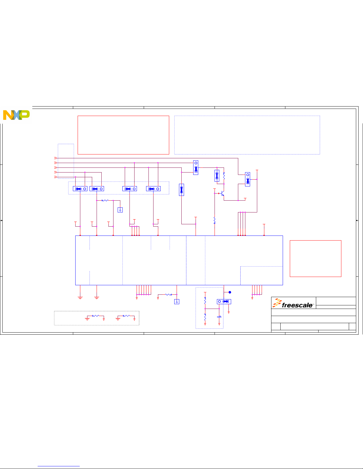
5
5
4
4
3
3
2
2
1
1
D D
C C
B B
A A
Individual MCU
supply control
jumpers
3v3
Default Configuraiton:
- ALL MCU supply voltages are set to 3.3V (ADC0, ADC1, VDD_HV_A,
VDD_HV_B, VDD_HV_C, VBallast)
- VDD_HV_FLA = External 3.3V supplied (jumper fitted)
- VDD_LV Supplied from ballast transistor
This is not necessarily the same as the default shown in the RM. All
VDD_HV_x domains have at least one peripheral that only functions at
3.3V. Therefore the default is to run these from 3.3V. The analogue pins
can only be driven to the same voltage as the VDD_HV_x domain they are
situated in (ie max 3.3V) so makes sense for the analogue supply and
reference to be 3.3V
Ground Links
(0 Ohm
Resistors)
3v3 5v0 5v0 5v0 5v03v3 3v3
3v3
3v3
5v0
MPC5748G MCU Power Connections
Caution:
- If VDD_HV_A is driven from 5V, the VDD_HV_FLA pin
must not be supplied from 3.3V (remove the HVA_FLA
jumper)
- Don't attempt to over drive an analogue pad to 5V
when the digital VDD_HV_x supply is set to 3.3V. This
will trigger the ESD protectrion on that pad. For
example if VDD_HV_A is set to 3.3V and the analogue
supplies are set to 5V, you cannot drive 5V into a
pad in the VDD_HV_A domain
Differences to 324BGA
- 2 fewer VDD_HV_A on 176QFP
- 1 fewer VDD_HV_B
- No VDD_HV_C
- 5 Fewer VDD_LV
- No VIN1_CMP_REF
- 15 Fewer VSS_LV
- 5 Fewer VSS_HV
- Heat Dissipation GND TAB
From MCU
supply
jumpers on
main board
INT_BAL_SELECT enable
MPC5746
Individual MCU
supply control
jumpers
MCU_3V3_S
MCU_5V0_S
MCU_1V25_L
MCU_3V3_L
MCU_5V0_L
HVB_CAP
HVFLA_CAP
LV_CAP
ADC0_CAP
ADC1_CAP
ADC1REF_CAP
ADC0_GND ADC1_GND
GND
HVA_CAP
GNDADC0_GND GNDADC1_GND
E_CAP
B_CAP
LVDEC_CAP
GND GNDGND
HVA_CAP
GND GND
MCU_1V25_L8
MCU_5V0_S8
MCU_3V3_S8
MCU_5V0_L8
MCU_3V3_L8
Drawing Title:
Size Document Number Rev
Date: Sheet
of
Page Title:
Automotive Microcontroller
Applications
East Kilbride, Scotland
SCH-27898 PDF: SPF-27898 D1
MPC5748G 176 QFP Daughter Card
B
Tuesday, August 18, 2015
MPC5748G MCU Power
28
Freescale General Business Use
Drawing Title:
Size Document Number Rev
Date: Sheet of
Page Title:
Automotive Microcontroller
Applications
East Kilbride, Scotland
SCH-27898 PDF: SPF-27898 D1
MPC5748G 176 QFP Daughter Card
B
Tuesday, August 18, 2015
MPC5748G MCU Power
28
Freescale General Business Use
Drawing Title:
Size Document Number Rev
Date: Sheet of
Page Title:
Automotive Microcontroller
Applications
East Kilbride, Scotland
SCH-27898 PDF: SPF-27898 D1
MPC5748G 176 QFP Daughter Card
B
Tuesday, August 18, 2015
MPC5748G MCU Power
28
Freescale General Business Use
C51
1.0 UF
DNP
R36
0
1.25v Core & External BallastAnalogue
MPC5748G 176QFP
Package 2of3 Power Pins
Flash
Central Pad for heat
dissipation & GND
U1B
PPC5748GSK0MKU6 + OTQ-176SG-0.5-004-00
VRC_CTRL
32
VSS_LV_109
109
VDD_LV_3131VDD_LV_54
54
VDD_LV_110
110
VDD_LV_152
152
VDD_HV_A_6
6
VDD_HV_A_5959VDD_HV_A_85
85
VDD_HV_A_151
151
VDD_HV_B_124
124
VSS_HV_ADC0
89
VDD_HV_ADC0
90
VDD_HV_ADC1
99
VSS_HV_ADC1
97
VDD_HV_FLA
27
VDD_HV_ADC1_REF
98
VSS_HV_77VSS_HV_2828VSS_HV_5555VSS_HV_5757VSS_HV_8686VSS_HV_123
123
VSS_HV_150
150
VDD_LP_DEC
30
VSS_HV_VPP
26
EX_PAD1
177
EX_PAD2
178
EX_PAD3
179
EX_PAD4
180
EX_PAD5
181
J9
1
2
3
J8
12
R38
10K
DNP
J5
123
R20
0
R27
0
R8
0
Q20
MJD31CT4
3 4
1
J3
123
TP107
TPAD_030
J14
12
J10
1
2
3
TPH2
1
J4
123
R39
1.0
DNP
R37
10K
J11
123
TPH1
1
J6
123
R9
0
Page 73
5
5
4
4
3
3
2
2
1
1
D D
C C
B B
A A
Capacitor Types:
470pF - Ceramic COG, 50v 5% 0402
1000pF - Ceramic COG, 50V 5% 0402
4700pF - Ceramic X7R, 50V 10% 0402
0.01uF - Ceramic X7R, 50V 10% 0402
0.1uF - Ceramic X7R, 16V 10% 0402
0.68uF - Ceramic X7R 16V 10% 0805 (Murata GCM219R71C684KA37 )
1.0uF - Ceraminc X7R, 10V 10% 0603 (Taiyo Yuden LMK107B7105KA-T)
2.2uF - Ceraminc X7R, 10V, 10%, 0603 (Taiyo Yuden LMK107B7225KA-TR)
4.7uF - TANT, 12.5V 20% ESR=0.08R 7343
10uF - TANT, 35V 10% ESR=0.125R CC7343-31
4.7uF Alternative (150-78844)- Polymer ALU, 16V 20% ESR=0.08R
7343-18
Place small Caps as close as possible to MCU pins
ADC
Place small caps close to each MCU pin
VDD_HVA VDD_HVB
VDD_LV
See caps below for Bypass Transistor bulk storage (some on VDD1V2 rail)
VDD_LV (1.25V) Decoupling. Place
as close as possible to pin.
Ballast Transistor
Flash
MPC5748G MCU Decoupling and bulk storage
LP Internal Reg Cap
Place
close to
transistor
Place one 0.68uF cap footprint
each side of package
Place 10uF cap to west side of package
(low ESR)
(low
ESR)
(low
ESR)
(Murata GCM219R71C684KA37)
(low
ESR)
(low
ESR)
(low
ESR)
(low
ESR)
(low ESR)
2.2uF caps
are DNP.
Place close
to emitter
One of these is DNP. May replace 2 caps with
0.47uF to keep overall capacitance within limits
Differences to 324BGA
- 2 Fewer VDD_HV_A capacitor pairs
- 1 fewer VDD_HV_B capacitor pair
- No VDD_HV_C capacitor pairs
- 5 fewer VDD_LV capacitor pairs
ADC0_CAP
ADC0_GND
ADC1REF_CAP
ADC1_GND
ADC1_CAP
ADC1_GND
GND
HVA_CAP
GND
HVB_CAP
LV_CAP
GND
HVFLA_CAP
GND
LV_CAPB_CAP E_CAP
GND
LVDEC_CAP
GND
E_CAP
GND
Drawing Title:
Size Document Number Rev
Date: Sheet
of
Page Title:
Automotive Microcontroller
Applications
East Kilbride, Scotland
SCH-27898 PDF: SPF-27898 D1
MPC5748G 176 QFP Daughter Card
B
Tuesday, August 18, 2015
MPC5748G MCU Decoupling
38
Freescale General Business Use
Drawing Title:
Size Document Number Rev
Date: Sheet of
Page Title:
Automotive Microcontroller
Applications
East Kilbride, Scotland
SCH-27898 PDF: SPF-27898 D1
MPC5748G 176 QFP Daughter Card
B
Tuesday, August 18, 2015
MPC5748G MCU Decoupling
38
Freescale General Business Use
Drawing Title:
Size Document Number Rev
Date: Sheet of
Page Title:
Automotive Microcontroller
Applications
East Kilbride, Scotland
SCH-27898 PDF: SPF-27898 D1
MPC5748G 176 QFP Daughter Card
B
Tuesday, August 18, 2015
MPC5748G MCU Decoupling
38
Freescale General Business Use
C25
0.1UF
C9
2.2UF
DNP
C43
1000pF
C46
1000pF
C40
1.0 UF
C47
0.1UF
C35
0.1UF
C28
0.68uF
DNP
C42
0.1UF
+
C2
10UF
C45
0.1UF
C44
1.0 UF
C29
0.1UF
C7 4700pF
C32
1000pF
+
C1
10UF
DNP
C34
1000pF
C8
2.2UF
DNP
+
C3
10UF
DNP
C22
0.1UF
C48
470pF
+
C4
10UF
DNP
C21
0.68uF
C27
470pF
C41
1000pF
C30
0.68uF
C26
0.1UF
C23
470pF
C37
0.1UF
C50
0.1UF
C31
2.2UF
LMK107B7225KA-T
C20
0.1UF
C49
0.68uF
C36
1uF
LMK107B7105KA-T
C33
1.0 UF
C24
1000pF
Page 74
5
5
4
4
3
3
2
2
1
1
D D
C C
B B
A A
MPC5748G GPIO 1 of 2
Key to text colours:
Purple - Comms Physical Interfaces
Blue - Debug (JTAG & Nexus)
(LIN0_RX)
(LIN0_TX)
(LIN1_TX)
(LIN1_RX)
(XTAL32)
(EXTAL32)
(FR_A_TX)
(FR_A_TX_EN)
(FR_A_RX)
(FR_B_TX_EN)
(FR_B_RX)
(FR_B_TX)
(USB1_CLK)
(USB1_D0)
(USB1_D1)
(USB1_D2)
(USB1_D3)
(USB1_D4)
(USB1_D5)
(USB1_D6)
(USB1_D7)
(USB1_DIR)
Orange - Other Peripherals and I/O
(RMII_RXD0)
(RMII_RXD1)
(MII_RXD2)
(MII_RXD3)
(MII_CRS)
(RMII_TXD0)
(RMII_TXD1)
(MII_TXD2)
(MII_TXD3)
(RMII_TXEN)
(RMII_MDC)
(RMII_TXCLK)
(RMII_RXDV)
(RMII_MDIO)
(RMII_RXER)
(MII_COL)
(MII_RXCLK)
(FR_DBG0)
(FR_DBG1)
(FR_DBG2)
(FR_DBG3)
(SD_CMD)
(SD_CLK)
(SD_WP)
(SAI0_D0)
(SAI0_D1)
(SAI0_D2)
(SAI0_D3)
(SAI0_BCLK)
(SAI0_MCLK)
(SAI0_SYNC)
(SAI1_SYNC)
(SAI1_MCLK)
(TDI)
(TDO)
(TCK)
(TMS)
Black - Clock, Reset and Control
(MLB_DN)
(MLB_DP)
(MLB_SN)
(MLB_SP / DAT)
(MLB_CN / SIG)
(SAI_I2C2_SCL)
(SAI_I2C2_SDA)
(SAI_I2C3_SDA)
(SAI_I2C3_SCL)
(MLB_I2C1_SCL)
(MLB_I2C1_SDA)
Green - I/O Matrix (dedicated)
(CMP1_8 / IO)
(CMP1_10 / IO)
(CMP1_11 /IO)
(CMP1_12 / IO)
(CMP1_13 / IO)
(CMP1_14 / IO)
(CMP1_15 / IO)
(CLKOUT1 GPIO)
(GPIO)
(GPIO)
(HEX1 & GPIO)
(HEX2 & GPIO)
(HEX3 & GPIO)
(HEX4 & GPIO)
(SW1 & GPIO**)
(SW2 & GPIO)
(LED1 & GPIO)
(LED2 & GPIO)
(LED3 & GPIO)
(LED4 & GPIO)
(MLB_RST)
(MLB_PWR)
(MLB_IRQ - WKPU21)
** PA1 is also NMI. Routed to I/O Matrix
RED - I/O Matrix and other functions (eg LED)
(CLKOUT0 GPIO)
(eMIOS1_UC_5H)
(eMIOS1_UC_6H)
(eMIOS1_UC_7H)
(ADC_POT)
(GPIO)
(GPIO)
(GPIO)
(GPIO)
(GPIO)
(GPIO)
(GPIO)
(GPIO)
(GPIO)
(GPIO)
(GPIO)
(GPIO)
(GPIO)
(GPIO)
(CAN0_TX)
(CAN0_RX)
(SW4 & GPIO)
(CAN1_RX)
(CAN1_TX)
(SW3 & GPIO)
(RS232_RX)
(RS232_TX)
(SD_CD - WKPU19)
(GPIO)
(GPIO)
(GPIO)
(eMIOS E1UC_11_H)
(eMIOS E1UC_12_H)
(eMIOS E1UC_13_H)
(eMIOS E1UC_14_H)
(WKPU2 / NMI0)
(WKPU3)
WKPU22
WKPU15
Differences to 324BGA
- Port D 11 Not on 176QFP
(SAI_GPIO)
(MLB_GPIO)
(GPIO & MLB_ST)
PA0
PA1
PA3
PA2
PA4
PA5
PA7
PA6
PA8
PA9
PA11
PA10
PA12
PA13
PA15
PA14
PB0
PB1
PB3
PB2
PB4
PB5
PB7
PB6
PB8
PB9
PB11
PB10
PB12
PB13
PB15
PB14
PC0
PC1
PC3
PC2
PC4
PC5
PC7
PC6
PC8
PC9
PC11
PC10
PC12
PC13
PC15
PC14
PD0
PD1
PD3
PD2
PD4
PD5
PD7
PD6
PD8
PD9
PD10
PD12
PD13
PD15
PD14
PE0
PE1
PE3
PE2
PE4
PE5
PE7
PE6
PE8
PE9
PE11
PE10
PE12
PE13
PE15
PE14
PF0
PF1
PF3
PF2
PF4
PF5
PF7
PF6
PF8
PF9
PF11
PF10
PF12
PF13
PF15
PF14
PG0
PG1
PG3
PG2
PG4
PG5
PG7
PG6
PG8
PG9
PG11
PG10
PG12
PG13
PG15
PG14
PH0
PH1
PH3
PH2
PH4
PH5
PH7
PH6
PH8
PH9
PH11
PH10
PH12
PH13
PH15
PH14
MCU-EXTAL
MCU-XTAL
PORSTx
MCU-RSTx
PH0
7
PORSTx
8
MCU-RSTx8
MCU-EXTAL
6
MCU-XTAL6
PB08
PB18
PB28
PB38
PB118
PB128
PB137
PB147
PB157
PB68
PB78
PB86
PB96
PB108
PA118
PA128
PA138
PA148
PA158
PA68
PA78
PA88
PA98
PA108
PA58
PA08
PA18
PA28
PA38
PA48
PB58
PB48
PC118
PC128
PC138
PC148
PC158
PC68
PC78
PC88
PC98
PC108
PC58
PC48
PC08
PC18
PC28
PC38
PD128
PD138
PD147
PD157
PD68
PD78
PD88
PD98
PD108
PD58
PD48
PD08
PD18
PD28
PD38
PH1
7
PH2
7
PH3
8
PH4
8
PH5
8
PH6
8
PH7
8
PH8
8
PH9
8
PH10
8
PH11
8
PH12
8
PH13
8
PH14
8
PH15
8
PG0
7
PG1
8
PG2
8
PG3
8
PG4
8
PG5
8
PG6
8
PG7
8
PG8
8
PG9
8
PG10
8
PG11
8
PG12
7
PG13
7
PG14
8
PG15
8
PF0
8
PF1
8
PF2
8
PF3
8
PF4
8
PF5
8
PF6
8
PF7
8
PF8
8
PF9
8
PF10
8
PF11
8
PF12
8
PF13
8
PF14
8
PF15
8
PE0
8
PE1
8
PE2
8
PE3
8
PE4
8
PE5
8
PE6
8
PE7
8
PE8
8
PE9
8
PE10
8
PE11
8
PE12
8
PE13
8
PE14
8
PE15
8
Drawing Title:
Size Document Number Rev
Date: Sheet
of
Page Title:
Automotive Microcontroller
Applications
East Kilbride, Scotland
SCH-27898 PDF: SPF-27898 D1
MPC5748G 176 QFP Daughter Card
B
Tuesday, August 18, 2015
MPC5748G GPIO 1of2
48
Freescale General Business Use
Drawing Title:
Size Document Number Rev
Date: Sheet of
Page Title:
Automotive Microcontroller
Applications
East Kilbride, Scotland
SCH-27898 PDF: SPF-27898 D1
MPC5748G 176 QFP Daughter Card
B
Tuesday, August 18, 2015
MPC5748G GPIO 1of2
48
Freescale General Business Use
Drawing Title:
Size Document Number Rev
Date: Sheet of
Page Title:
Automotive Microcontroller
Applications
East Kilbride, Scotland
SCH-27898 PDF: SPF-27898 D1
MPC5748G 176 QFP Daughter Card
B
Tuesday, August 18, 2015
MPC5748G GPIO 1of2
48
Freescale General Business Use
MPC5748G 176QFP
Package 1of3 GPIO Pins1
U1A
PPC5748GSK0MKU6 + OTQ-176SG-0.5-004-00
RESET
29
PORST
153
XTAL
56
EXTAL
58
PA0
24
PA1
19
PA2
17
PA3
114
PA4
51
PA5
146
PA6
147
PA7
128
PA8
129
PA9
130
PA10
131
PA11
132
PA12
53
PA13
52
PA14
50
PA15
48
PB0
39
PB1
40
PB2
176
PB3
1
PB4
88
PB5
91
PB6
92
PB7
93
PB8
61
PB9
60
PB10
62
PB11
96
PB12
101
PB13
103
PB14
105
PB15
107
PC0
154
PC1
149
PC2
145
PC3
144
PC4
159
PC5
158
PC6
44
PC7
45
PC8
175
PC9
2
PC10
36
PC11
35
PC12
173
PC13
174
PC14
3
PC15
4
PD0
77
PD1
78
PD2
79
PD3
80
PD4
81
PD5
82
PD6
83
PD7
84
PD8
87
PD9
94
PD10
95
PD12
100
PD13
102
PD14
104
PD15
106
PE0
18
PE1
20
PE2
156
PE3
157
PE4
160
PE5
161
PE6
167
PE7
168
PE8
21
PE9
22
PE10
23
PE11
25
PE12
133
PE13
127
PE14
136
PE15
137
PF0
63
PF1
64
PF2
65
PF3
66
PF4
67
PF5
68
PF6
69
PF7
70
PF8
42
PF9
41
PF10
46
PF11
47
PF12
43
PF13
49
PF14
126
PF15
125
PG0
122
PG1
121
PG2
16
PG3
15
PG4
14
PG5
13
PG6
38
PG7
37
PG8
34
PG9
33
PG10
138
PG11
139
PG12
116
PG13
115
PG14
134
PG15
135
PH0
117
PH1
118
PH2
119
PH3
120
PH4
162
PH5
163
PH6
164
PH7
165
PH8
166
PH9
155
PH10
148
PH11
140
PH12
141
PH13
9
PH14
10
PH15
8
Page 75
5
5
4
4
3
3
2
2
1
1
D D
C C
B B
A A
MPC5748G GPIO 2 of 2
(USB1_NXT)
(USB1_STP)
(SD_D3)
(SD_D2)
(SD_D1)
(SD_D0)
(SAI1_D0)
(SAI1_BCLK)
(SAI2_D0)
(SAI2_BCLK)
(SAI2_MCLK)
(SAI2_SYNC)
(MLB_CP / CLK)
(GPIO)
(GPIO)
(USB1_RST)
(USB0_RST)
(ENET_RST)
Green - I/O Matrix (dedicated)
Key to text colours:
Purple - Comms Physical Interfaces
Blue - Debug (JTAG & Nexus)
RED - I/O Matrix and other functions (eg LED)
Orange - Other Peripherals and I/O
Black - Clock, Reset and Control
Differences to 324BGA
- 2 fewer pins on Port I
- 12 fewer pins on Port J
- No Ports K to Q
(And corresponding changes
to daughtercard connectors)
(GPIO & MLB_PS0)
(GPIO & MLB_PS1)
PI0
PI1
PI3
PI2
PI4
PI5
PI7
PI6
PI8
PI11
PI12
PI13
PI15
PI14
PJ0
PJ1
PJ3
PJ2
PJ4
PI118
PI128
PI138
PI148
PI158
PI68
PI78
PI87
PI58
PI08
PI18
PI28
PI38
PI48
PJ08
PJ18
PJ28
PJ38
PJ48
Drawing Title:
Size Document Number Rev
Date: Sheet
of
Page Title:
Automotive Microcontroller
Applications
East Kilbride, Scotland
SCH-27898 PDF: SPF-27898 D1
MPC5748G 176 QFP Daughter Card
B
Tuesday, August 18, 2015
MPC5748G GPIO 2of2
58
Freescale General Business Use
Drawing Title:
Size Document Number Rev
Date: Sheet of
Page Title:
Automotive Microcontroller
Applications
East Kilbride, Scotland
SCH-27898 PDF: SPF-27898 D1
MPC5748G 176 QFP Daughter Card
B
Tuesday, August 18, 2015
MPC5748G GPIO 2of2
58
Freescale General Business Use
Drawing Title:
Size Document Number Rev
Date: Sheet of
Page Title:
Automotive Microcontroller
Applications
East Kilbride, Scotland
SCH-27898 PDF: SPF-27898 D1
MPC5748G 176 QFP Daughter Card
B
Tuesday, August 18, 2015
MPC5748G GPIO 2of2
58
Freescale General Business Use
MPC5748G 176QFP
Package 3of3 GPIO Pins2
U1C
PPC5748GSK0MKU6 + OTQ-176SG-0.5-004-00
PI0
172
PI1
171
PI2
170
PI3
169
PI4
143
PI5
142
PI6
11
PI7
12
PI8
108
PI11
111
PI12
112
PI13
113
PI14
76
PI15
75
PJ0
74
PJ1
73
PJ2
72
PJ3
71
PJ4
5
Page 76
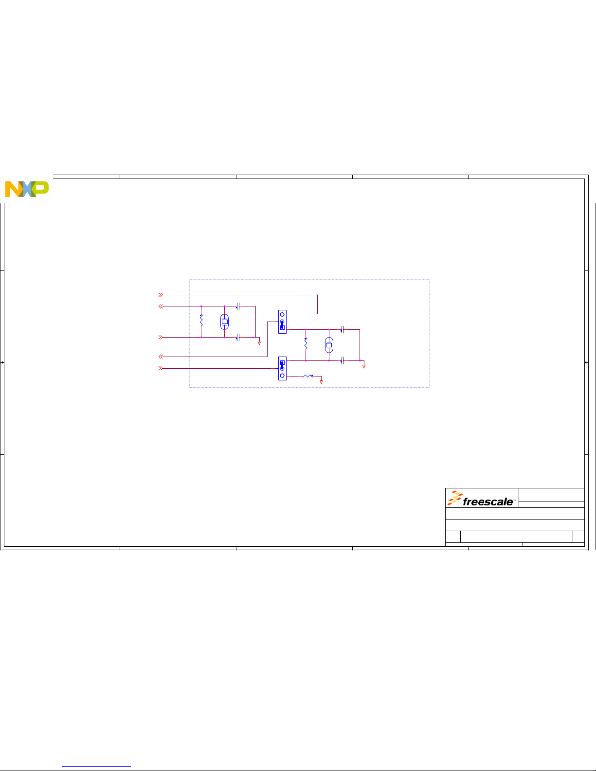
5
5
4
4
3
3
2
2
1
1
D D
C C
B B
A A
Oscillators and External Clock
(XTAL32)
(EXTAL32)
NX8045GB-40.000M-STD-CSJ-1 XTAL
(Optimised for Automotive, 8pF Load capacitance)
FC-255 32.7680K-A3
(Load Capacitance 7pF)
(From SMA connector on main board)
Clocks
EXTAL
MCU-XTAL
PB8
MCU-EXTAL
XTAL
PB9
EXT-CLK
GND
GND
GND
MCU-XTAL
4
PB8
4
PB94
MCU-EXTAL4
EXT-CLK
8
Drawing Title:
Size Document Number Rev
Date: Sheet
of
Page Title:
Automotive Microcontroller
Applications
East Kilbride, Scotland
SCH-27898 PDF: SPF-27898 D1
MPC5748G 176 QFP Daughter Card
B
Tuesday, August 18, 2015
Clocks
68
Freescale General Business Use
Drawing Title:
Size Document Number Rev
Date: Sheet of
Page Title:
Automotive Microcontroller
Applications
East Kilbride, Scotland
SCH-27898 PDF: SPF-27898 D1
MPC5748G 176 QFP Daughter Card
B
Tuesday, August 18, 2015
Clocks
68
Freescale General Business Use
Drawing Title:
Size Document Number Rev
Date: Sheet of
Page Title:
Automotive Microcontroller
Applications
East Kilbride, Scotland
SCH-27898 PDF: SPF-27898 D1
MPC5748G 176 QFP Daughter Card
B
Tuesday, August 18, 2015
Clocks
68
Freescale General Business Use
J1
1
2
3
C6
12PF
C38 12PF
R35 0
DNP
R7
1.0M
DNP
Y20
32.768KHZ
1 2
C39
12PF
R30
1.0M
DNP
Y1
40.0MHZ
12
J2
1
2
3
C5
12PF
Page 77
5
5
4
4
3
3
2
2
1
1
D D
C C
B B
A A
(PD[15] Shared with MLB_DAT for 3-pin mode)
(PB[15] Shared with MLB_SIG for 3-pin mode)
(PI[8] Shared with MLB_CLK for 3-pin mode)
Place resistors as close as possible to MCU
R1 Fitted by default
for LVDS 6-pin signals
Remove R1 and
fit R2 to
enable 3-pin
signals
Layout Note - Place resistors as shown with
shared pad (as close to MCU as possible)
Place resistors as close as possible to MCU
From MCU To Daughtercard
MLB Termination
Ethernet Termination
High Speed Signal Termination
PB14
PD15
PB13
PD14
PI8
MLB_SN
MLB_SP
MLB_DN
MLB_DP
MLB_CN
MLB_CP
PB15
MLB_CLK
MLB_SIG
MLB_DAT
PH2
PH1
PG12
PH0
PG13
PH2-R
PH1-R
PH0-R
PG13-R
PG12-R
PG0-RPG0
PI8
5
PB144
PB154
PB134
MLB_DAT
8
MLB_SIG
8
MLB_CLK
8
MLB_SN
8
MLB_SP
8
MLB_DN
8
MLB_DP
8
MLB_CN
8
MLB_CP
8
PG13
4
PG12
4
PH0
4
PH1
4
PH2
4
PG13-R
8
PG12-R
8
PH0-R
8
PH1-R
8
PH2-R
8
PG0-R
8
PG0
4
PD15
4
PD14
4
Drawing Title:
Size Document Number Rev
Date: Sheet
of
Page Title:
Automotive Microcontroller
Applications
East Kilbride, Scotland
SCH-27898 PDF: SPF-27898 D1
MPC5748G 176 QFP Daughter Card
B
Tuesday, August 18, 2015
High Speed Signal Termination
78
Freescale General Business Use
Drawing Title:
Size Document Number Rev
Date: Sheet of
Page Title:
Automotive Microcontroller
Applications
East Kilbride, Scotland
SCH-27898 PDF: SPF-27898 D1
MPC5748G 176 QFP Daughter Card
B
Tuesday, August 18, 2015
High Speed Signal Termination
78
Freescale General Business Use
Drawing Title:
Size Document Number Rev
Date: Sheet of
Page Title:
Automotive Microcontroller
Applications
East Kilbride, Scotland
SCH-27898 PDF: SPF-27898 D1
MPC5748G 176 QFP Daughter Card
B
Tuesday, August 18, 2015
High Speed Signal Termination
78
Freescale General Business Use
R2 50
R24
0
R33
0
R22
0
R23 100 1%
R34
100
DNP
R5 50
R32 105.0 1%
R1 50
R6 50
R21
100
DNP
R26
0
R28 105.0 1%
R4 50
R25
100
DNP
R3 50
R29
0
R31
0
Page 78
5
5
4
4
3
3
2
2
1
1
D D
C C
B B
A A
Daughter Card Connectors (Plugs)
Notes:
- there was no neat way to fit these connectors onto a B sized sheet so unfortunately the
sheet size has been increased to C so will need to be printed on larger paper.
- The Crystal Signals are NOT routed via the daughtercard connectors
- The Specific MCU power pins are not routed via the daughter card however the jumpered MCU
supply lines are brought up from the main board (see the top pins of the connector on the
left)
- The connector schematic symbols have been horizontally mirrored so they match the main EVB
connector. This has no bearing on the PCB placement or footprint. Pin1 on the recepticle
mates with pin 1 on the plug.
(GND)
(GND)
(GND)
(GND)
(GND)
(GND)
(GND)
(PK9)
(PK11)
(PK14)
(PK12)
(PP8)
(PP11)
(PP3)
(PL0)
(PO1)
(PP4)
(PO11)
(PO8)
(PO13)
(PO15)
(PP1)
(PO6)
(PN15)
(PO3)
(PO2)
(PN12)
(PN8)
(PN7)
(PK1)
(PN4)
(PK3)
(PK5)
(PN5)
(PK7)
(PN2)
(PJ12)
(PJ15)
(PJ14)
(PN3)
(PK15)
(PN6)
(PN0)
(PP10)
(PP5)
(PO0)
(PP2)
(PK2)
(PP7)
(PK4)
(PK6)
(PP6)
(PK8)
(PJ11)
(PP9)
(PJ10)
(PO12)
(PK0)
(PO7)
(PJ9)
(PO10)
(PJ13)
(PO4)
(PO9)
(PO14)
(PP0)
(PO5)
(PN14)
(PN13)
(PN11)
(PN9)
(PK10)
(PN10)
(PK13)
(GND)
(GND) (GND)
(GND)
Plug
(GND)
(GND)
(GND)
(GND)
(GND)
(GND)
(GND)
(GND)
(GND)
(GND)
(GND)
(GND)
(GND)
(GND)
(GND)
(GND)
(GND)
(GND)
(GND)
(GND)
(GND)
(GND)(GND)
(GND)
(GND)
(GND)
(GND)
(GND)
(GND)
(GND)
(GND)
(GND)
(GND)
(GND)
(GND)
(GND)
(GND)
(GND)
(GND)
(GND)
(GND)
(GND)
(GND)
(PM15)
(PM3)
(PM12)
(PM14)
(PQ0)
(PL9)
(PM4)
(PQ4)
(PL1)
(PL3)
(PQ5)
(PM5)
(PQ7)
(PJ5)
(PL12)
(PP15)
(PJ7)
(GND)
(GND)
(GND)(GND)
(GND) (GND)
(GND)
(GND)
(GND)
(GND)
(GND)
(GND)
(GND)
(GND)
(GND)
(GND)
(GND)
(GND)
(GND)
(GND)
(GND)
(GND)
(GND)
(GND)
(GND)
(GND)
(GND)
(GND)
(GND)
(GND)
(GND)
(GND)
(GND)
(GND)
(GND)
(GND)
(GND)
(GND)
(GND)
(GND)
(GND)
Plug
(GND)(GND)
(PQ3)
(PL11)
(PL6)
(PD11)
(PQ1)
(PJ6)
(PJ8)
(PQ2)
(PL7)
(PL15)
(PI10)
(PQ6)
(PI9)
(PM2)
(PM1)
(PL8)
(PL4)
(PL10)
(PL13)
(PL5)
(PM9)
(PL14)
(PM0)
(PM8) (PM10)
(PM7)
(PM6)
(PP13)
(PP14)
(PP12)
(PM13)
(PN1)
(PM11)
(PL2)
Connectors on Main board (Shown for reference)
PE6
PI3
PI1
PI2
PC13
PI0
PB2
EXT-CLK
MCU_3V3_S
MCU_3V3_L
MCU_5V0_L
PB3
PA12
PF0
PF1
PH8
PH7
PH6
PE7
PC12
PA13
PC8
PC9
PC15
PC14
PJ4
PF10
PH14
PG5
PH13
PG4
PI7 PH15
PE10
PE1 PE0
PI6
PE11 PG2
PC7
PG3 PA2
PE9
PE8 PA1
MCU-RSTx
PF8
PC6
PG9
PF13
PA0
MCU_5V0_S
MCU_1V25_L
PG7 PG6
PG8 PC11
PC10
PB0
PB10
PA15
PA4
PB1
PF12
PF11
PF9
PA14
PF3
PF4
PF7
PE5
PG14
PC5
PI5 PC3
PE4
PC2
PC0
PH2-R
PA8
PA9
PF14
PG0-R
PG1
PA7
PA10
PE13
PF15
PE12
PA11
PA3
PH0-R
PH1-R
PH9
PG13-R
PG12-R
PI13
PC1
PB12
PH10
PH5PH4
PE3
PE15
PH12
PG10
PG11
PE14
PH11
PORSTx
PC4
PG15
PE2
PA5
PA6
PI4
PF5
PJ2
PJ3
PD8
PF2
PB4
PD7
PB5
PD5
PJ0
PB11
PD1
PJ1
MLB_DP
MLB_DN
PB6
PD0
PD4
PF6
PI14
PD2
PD6
PD3
MLB_CP
MLB_DAT
MLB_CLK
MLB_CN
MLB_SN
MLB_SIG
MLB_SP
PH3
PI11
PI12
PD9
PD12
PI15
PD13
PB7
PD10
DC_5V0_S
DC_P12V
DC_1V25_L DC_5V0_L
DC_3V3_L
DC_3V3_S
GND GND
GNDGND
PC154
PG5
4
PI7
5
PE1
4
PI6
5
PE11
4
PG3
4
PE84
PG9
4
PA0
4
PG7
4
PG8
4
PC10
4
PB14
PF9
4
PA14
4
PE6
4
PI3
5
PA4
4
PI15
PI2
5
PC13
4
PI0
5
PA15
4
PB2
4
PB104
EXT-CLK
6
MCU_3V3_S 2
MCU_3V3_L 2
MCU_5V0_L 2
PA12
4
PF1
4
PF0
4
PA13
4
PF10
4
PC7
4
PF8
4
PC6
4
PF134
MCU_5V0_S2
MCU_1V25_L2
PH7
4
PH6
4
PB3
4
PH8
4
PE7
4
PC12
4
PC9
4
PC14
4
PJ4
5
PH14
4
PH13
4
PG4
4
PH15
4
PE10
4
PE0
4
PG2
4
PA2
4
PE9
4
PA1
4
MCU-RSTx
4
PG6
4
PC11
4
PB0
4
PF12
4
PF11
4
PC8
4
PF4
4
PF7
4
PF3
4
PC0
4
PH9
4
MLB_DP
7
MLB_DN
7
PC1
4
PH5
4
PE3
4
PE4
4
PC3
4
PE15
4
PORSTx
4
PE2
4
PG11
4
PG10
4
PI4
5
PA9
4
PA10
4
PA8
4
PG0-R
7
PF14
4
PG12-R
7
PH2-R
7
PG13-R
7
PB12
4
PI13
5
PD9
4
PB7
4
PI12
5
MLB_CN
7
PI15
5
MLB_CP
7
PI14
5
PD6
4
PD3
4
PD2
4
PD0
4
PB6
4
PF6
4
PD4
4
PH10
4
PE5
4
PH4
4
PI5
5
PG14
4
PC5
4
PH12
4
PC4
4
PC2
4
PA6
4
PA5
4
PH11
4
PE14
4
PG15
4
PE12
4
PA11
4
PE13
4
PA7
4
PG1
4
PF15
4
PH1-R
7
PA3
4
PH0-R
7
PH3
4
PD12
4
PD13
4
PI11
5
MLB_DAT
7
PD10
4
MLB_CLK
7
MLB_SIG
7
MLB_SN
7
PD7
4
MLB_SP
7
PD5
4
PJ0
5
PB11
4
PB5
4
PJ1
5
PD14
PD8
4
PF5
4
PB4
4
PJ3
5
PJ2
5
PF2
4
Drawing Title:
Size Document Number Rev
Date: Sheet
of
Page Title:
Automotive Microcontroller
Applications
East Kilbride, Scotland
SCH-27898 PDF: SPF-27898 D1
MPC5748G 176 QFP Daughter Card
C
Tuesday, August 18, 2015
Daughter Card Connectors (Plugs)
88
Freescale General Business Use
Drawing Title:
Size Document Number Rev
Date: Sheet of
Page Title:
Automotive Microcontroller
Applications
East Kilbride, Scotland
SCH-27898 PDF: SPF-27898 D1
MPC5748G 176 QFP Daughter Card
C
Tuesday, August 18, 2015
Daughter Card Connectors (Plugs)
88
Freescale General Business Use
Drawing Title:
Size Document Number Rev
Date: Sheet of
Page Title:
Automotive Microcontroller
Applications
East Kilbride, Scotland
SCH-27898 PDF: SPF-27898 D1
MPC5748G 176 QFP Daughter Card
C
Tuesday, August 18, 2015
Daughter Card Connectors (Plugs)
88
Freescale General Business Use
TPV4
TPV6
TPV5
TPV1
P21
PLUG 180
2
SH1SH2
SH5SH6
1
43
65
87
109
1211
1413
1615
1817
2019
2221
2423
2625
2827
3029
3231
3433
3635
3837
4039
4241
4443
4645
4847
5049
5251
5453
5655
5857
6059
SH3SH4
6261
6463
6665
6867
7069
7271
7473
7675
7877
8079
8281
8483
8685
8887
9089
9291
9493
9695
9897
10099
102101
104103
106105
108107
110109
112111
114113
116115
118117
120119
SH7SH8
SH9SH10
122121
124123
126125
128127
130129
132131
134133
136135
138137
140139
142141
144143
146145
148147
150149
152151
154153
156155
158157
160159
162161
164163
166165
168167
170169
172171
174173
176175
178177
180179
SH11SH12
TPV3
P20
PLUG 180
2
SH1SH2
SH5SH6
1
43
65
87
109
1211
1413
1615
1817
2019
2221
2423
2625
2827
3029
3231
3433
3635
3837
4039
4241
4443
4645
4847
5049
5251
5453
5655
5857
6059
SH3SH4
6261
6463
6665
6867
7069
7271
7473
7675
7877
8079
8281
8483
8685
8887
9089
9291
9493
9695
9897
10099
102101
104103
106105
108107
110109
112111
114113
116115
118117
120119
SH7SH8
SH9SH10
122121
124123
126125
128127
130129
132131
134133
136135
138137
140139
142141
144143
146145
148147
150149
152151
154153
156155
158157
160159
162161
164163
166165
168167
170169
172171
174173
176175
178177
180179
SH11SH12
TPV2
Page 79

100 QFP DC
Page 80
5
5
4
4
3
3
2
2
1
1
D D
C C
B B
A A
Freescale AISG Applications, East Kilbride
X2
Revision Information
Designer CommentsRev Date
GPIO - MPC5746C GPIO pins 1 of 2
Clocks
Sheet 8
Sheet 2
Sheet 3
Sheet 4
Sheet 5
Sheet 6
Sheet 7
GPIO - MPC5746C GPIO pins 2 of 2
Table Of Contents:
MPC5746C Customer EVB 100 BGA Daughter Card (MPC574XG-100DS)
X1
Power - MPC5746C power pins footprint
Power - MPC5746C Decoupling Capacitors
Daughtercard Connectors
Bus Termination
05 Jan 2014 Alasdair Robertson Initial release sent for review based on X-MPC574XG-256DS RevA
These schematics are provided for reference purposes only. As such,
Freescale does not make any warranty, implied or otherwise, as to the
suitability of circuit design or component selection (type or value) used in
these schematics for hardware design using the Freescale MPC5746C family
of Microprocessors. Customers using any part of these schematics as a
basis for hardware design, do so at their own risk and Freescale does not
assume any liability for such a hardware design.
User notes are given throughtout the schematics.
Specific PCB LAYOUT notes are detailed in ITALICS
Caution:
Notes:
- All components and board processes are to be ROHS compliant
- All small capacitors are 0402 unless otherwise stated
- All resistors are 0603 5% 0.1w unless otherwise stated. All zero ohm links are 0603
- All connectors and headers are denoted Px and are 2.54mm pitch unless otherwise stated
- All jumpers are denoted Jx. Jumpers are 2mm pitch
- Jumper default positions are shown in the schematics. For 3 way jumpers, default is always posn 1-2.
2 Pin jumpers generally have the "source" on pin 1.
- All switches are denoted SWx
- All test points are denoted TPx
- Test point Vias are denoted TPVx
07 Jan 2014 Alasdair Robertson Post review corrections incl MCU Orcad Footprint
30 Jan 2014 Alasdair Robertson Prototype build releaseA
A1 18 Aug 2015 Alasdair Robertson Tidy up Schematics for UM (RevA PCB)
Drawing Title:
Size Document Number Rev
Date: Sheet
of
Page Title:
Designer:
Drawn by:
Approved:
Automotive Microcontroller Applications
East Kilbride, Scotland
This document contains information proprietary to Freescale and shall not be used for engineering design,
procurement or manufacture in whole or in part without the express written permission of Freescale
SCH-28701 PDF: SPF-28701 A1
MPC5746C 100 BGA Daughter Card
B
Tuesday, August 18, 2015
Index and Title Page
A. Robertson
A. Robertson
A. Robertson
18
Freescale General Business Use
Drawing Title:
Size Document Number Rev
Date: Sheet
of
Page Title:
Designer:
Drawn by:
Approved:
Automotive Microcontroller Applications
East Kilbride, Scotland
This document contains information proprietary to Freescale and shall not be used for engineering design,
procurement or manufacture in whole or in part without the express written permission of Freescale
SCH-28701 PDF: SPF-28701 A1
MPC5746C 100 BGA Daughter Card
B
Tuesday, August 18, 2015
Index and Title Page
A. Robertson
A. Robertson
A. Robertson
18
Freescale General Business Use
Drawing Title:
Size Document Number Rev
Date: Sheet
of
Page Title:
Designer:
Drawn by:
Approved:
Automotive Microcontroller Applications
East Kilbride, Scotland
This document contains information proprietary to Freescale and shall not be used for engineering design,
procurement or manufacture in whole or in part without the express written permission of Freescale
SCH-28701 PDF: SPF-28701 A1
MPC5746C 100 BGA Daughter Card
B
Tuesday, August 18, 2015
Index and Title Page
A. Robertson
A. Robertson
A. Robertson
18
Freescale General Business Use
Page 81
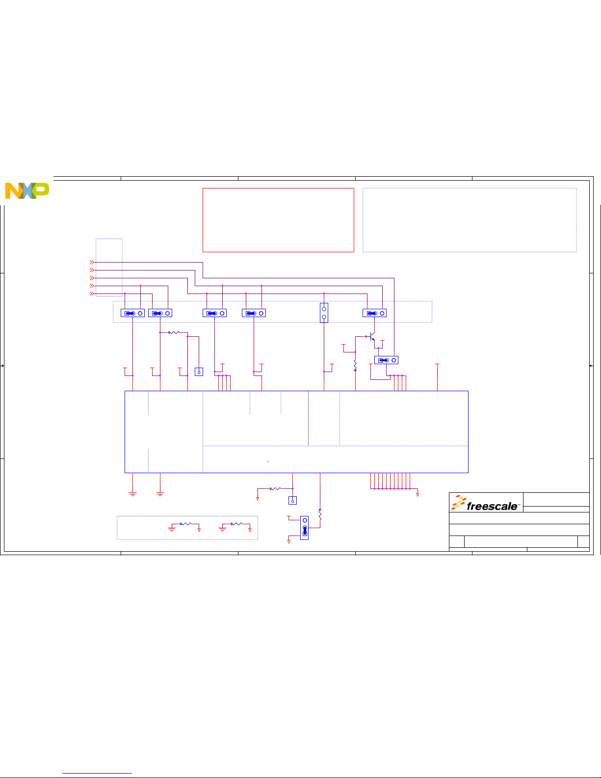
5
5
4
4
3
3
2
2
1
1
D D
C C
B B
A A
Individual MCU
supply control
jumpers
3v3
Default Configuraiton:
- ALL MCU supply voltages are set to 3.3V (ADC0, ADC1, VDD_HV_A,
VDD_HV_B, VDD_HV_C, VBallast)
- VDD_HV_FLA = External 3.3V supplied (jumper fitted)
- VDD_LV Supplied from ballast transistor
This is not necessarily the same as the default shown in the RM. All
VDD_HV_x domains have at least one peripheral that only functions at
3.3V. Therefore the default is to run these from 3.3V. The analogue pins
can only be driven to the same voltage as the VDD_HV_x domain they are
situated in (ie max 3.3V) so makes sense for the analogue supply and
reference to be 3.3V
Ground Links
(0 Ohm
Resistors)
3v3 5v0 5v0 5v0 5v03v3 3v3
3v3
3v3 5v0
MPC5746C MCU Power Connections
Caution:
- If VDD_HV_A is driven from 5V, the VDD_HV_FLA pin
must not be supplied from 3.3V (remove the HVA_FLA
jumper)
- Don't attempt to over drive an analogue pad to 5V
when the digital VDD_HV_x supply is set to 3.3V. This
will trigger the ESD protectrion on that pad. For
example if VDD_HV_A is set to 3.3V and the analogue
supplies are set to 5V, you cannot drive 5V into a
pad in the VDD_HV_A domain
From MCU
supply
jumpers on
main board
MCU_3V3_S
MCU_5V0_S
MCU_1V25_L
MCU_3V3_L
MCU_5V0_L
HVB_CAP
HVFLA_CAP
LV_CAP
ADC0_CAP
ADC1_CAP
ADC1REF_CAP
ADC0_GND ADC1_GND GND
HVA_CAP
GNDADC0_GND GNDADC1_GND
E_CAP
B_CAP
LVDEC_CAP
GND
HVA_CAP
GND
MCU_1V25_L8
MCU_5V0_S8
MCU_3V3_S8
MCU_5V0_L8
MCU_3V3_L8
Drawing Title:
Size Document Number Rev
Date: Sheet
of
Page Title:
Automotive Microcontroller
Applications
East Kilbride, Scotland
SCH-28701 PDF: SPF-28701 A1
MPC5746C 100 BGA Daughter Card
B
Tuesday, August 18, 2015
MPC5746C MCU Power
28
Freescale General Business Use
Drawing Title:
Size Document Number Rev
Date: Sheet of
Page Title:
Automotive Microcontroller
Applications
East Kilbride, Scotland
SCH-28701 PDF: SPF-28701 A1
MPC5746C 100 BGA Daughter Card
B
Tuesday, August 18, 2015
MPC5746C MCU Power
28
Freescale General Business Use
Drawing Title:
Size Document Number Rev
Date: Sheet of
Page Title:
Automotive Microcontroller
Applications
East Kilbride, Scotland
SCH-28701 PDF: SPF-28701 A1
MPC5746C 100 BGA Daughter Card
B
Tuesday, August 18, 2015
MPC5746C MCU Power
28
Freescale General Business Use
R35
0
J9
123
R37
1.0K
J8
HDR 1X2
12
R24
0
J5
123
R7
0
R10
0
1.25v Core & External BallastAnalogue
MPC5746C 100 BGA
Package 2of3 Power Pins
Flash
U1B
SKT BGA 100 TH + MPC574XG-100
VRC_CTRL
E1
VSS_D1D1VSS_E4E4VSS_E5E5VSS_E6E6VSS_E7E7VSS_F4F4VSS_F5F5VSS_F6F6VSS_F7F7VSS_K4K4VSS_K7
K7
INT_BAL_SEL
E2
VDD_LV_D5D5VDD_LV_D6
D6
VDD_LV_G5G5VDD_LV_G6
G6
VDD_HV_A_D4
D4
VDD_HV_A_G4
G4
VDD_HV_A_D7
D7
VDD_HV_B_E8
E8
VSS_HV_ADC0
K9
VDD_HV_ADC0
K10
VDD_HV_ADC1
G10
VSS_HV_ADC1
H10
VDD_HV_FLA_H3
H3
VDD_HV_ADC1_REF
H9
VDD_LP_DEC
F2
VSS_VPP
D2
VDD_HV_A_G7
G7
Q20
MJD31CT4
3 4
1
J3
123
J10
123
TPH2
1
J4
123
TPH1
1
J6
123
R9
0
J12
1
2
3
Page 82
5
5
4
4
3
3
2
2
1
1
D D
C C
B B
A A
Capacitor Types:
470pF - Ceramic COG, 50v 5% 0402
1000pF - Ceramic COG, 50V 5% 0402
4700pF - Ceramic X7R, 50V 10% 0402
0.01uF - Ceramic X7R, 50V 10% 0402
0.1uF - Ceramic X7R, 16V 10% 0402
0.68uF - Ceramic X7R 16V 10% 0805 (Murata GCM219R71C684KA37 )
1.0uF - Ceraminc X7R, 10V 10% 0603 (Taiyo Yuden LMK107B7105KA-T)
2.2uF - Ceraminc X7R, 10V, 10%, 0603 (Taiyo Yuden LMK107B7225KA-TR)
4.7uF - TANT, 12.5V 20% ESR=0.08R 7343
10uF - TANT, 35V 10% ESR=0.125R CC7343-31
4.7uF Alternative (150-78844)- Polymer ALU, 16V 20% ESR=0.08R
7343-18
Place small Caps as close as possible to MCU pins
ADC
Place small caps close to each MCU pin
VDD_HVA VDD_HVB
VDD_LV
VDD_LV (1.25V) Decoupling. Place -.1uF
caps as close as possible to respective
VDD_LV pins
Ballast Transistor
Flash
MPC5746C MCU Decoupling and bulk storage
LP Internal Reg Cap
Place close
to transistor
Place one 0.68uF cap footprint
each side of package
(low ESR)
(low
ESR)
(low
ESR)
(Murata GCM219R71C684KA37)
(low
ESR)
(low
ESR)
(low
ESR)
(low
ESR)
(low ESR)
2.2uF caps are
DNP. Place close
to emitter
One of these is DNP to keep overall capacitance less
than max spec of 3uF. If necessary, these can be
replaced with 0.47uF caps as long as combined ESR of all
caps is less than 0.03 Ohms
ADC0_CAP
ADC0_GND
ADC1REF_CAP
ADC1_GND
ADC1_CAP
ADC1_GND
GND
HVA_CAP
GND
HVB_CAP
LV_CAP
GND
HVFLA_CAP
GND
LV_CAPB_CAP E_CAP
GND
LVDEC_CAP
GND
E_CAP
GND
Drawing Title:
Size Document Number Rev
Date: Sheet
of
Page Title:
Automotive Microcontroller
Applications
East Kilbride, Scotland
SCH-28701 PDF: SPF-28701 A1
MPC5746C 100 BGA Daughter Card
B
Tuesday, August 18, 2015
MPC5746C MCU Decoupling
38
Freescale General Business Use
Drawing Title:
Size Document Number Rev
Date: Sheet of
Page Title:
Automotive Microcontroller
Applications
East Kilbride, Scotland
SCH-28701 PDF: SPF-28701 A1
MPC5746C 100 BGA Daughter Card
B
Tuesday, August 18, 2015
MPC5746C MCU Decoupling
38
Freescale General Business Use
Drawing Title:
Size Document Number Rev
Date: Sheet of
Page Title:
Automotive Microcontroller
Applications
East Kilbride, Scotland
SCH-28701 PDF: SPF-28701 A1
MPC5746C 100 BGA Daughter Card
B
Tuesday, August 18, 2015
MPC5746C MCU Decoupling
38
Freescale General Business Use
C52
0.1UF
C10
2.2UF
DNP
C48
1000pF
C54
1000pF
C57
1.0 UF
C23
0.1UF
C55
0.1UF
C20
0.68uF
DNP
C56
0.1UF
+
C1
10UF
C53
0.1UF
C59
1.0 UF
C39
0.1UF
C8 4700pF
C36
1000pF
+
C4
10UF
DNP
C46
1000pF
C9
2.2UF
DNP
+
C3
10UF
DNP
C35
0.1UF
C22
470pF
+
C2
10UF
DNP
C31
0.68uF
C27
470pF
C47
1000pF
C60
0.68uF
C26
0.1UF
C33
470pF
C32
0.1UF
C24
0.1UF
C34
2.2UF
LMK107B7225KA-T
C49
0.1UF
C29
0.68uF
C43
1uF
LMK107B7105KA-T
C58
1.0 UF
C51
1000pF
Page 83
5
5
4
4
3
3
2
2
1
1
D D
C C
B B
A A
MPC5746C GPIO 1 of 2
Key to text colours:
Purple - Comms Physical Interfaces
Blue - Debug (JTAG & Nexus)
(FR_A_TX)
(FR_A_TX_EN)
(FR_A_RX)
(USB1_D0)
(USB1_D1)
(USB1_D3)
(USB1_D5)
(USB1_D7)
Orange - Other Peripherals and I/O
(RMII_RXD0)
(RMII_RXD1)
(MII_RXD2)
(MII_RXD3)
(RMII_TXD0)
(RMII_TXD1)
(MII_TXD2)
(MII_TXD3)
(RMII_TXEN)
(RMII_MDC)
(RMII_TXCLK)
(RMII_RXDV)
(RMII_MDIO)
(RMII_RXER)
(MII_COL)
(MII_RXCLK)
(SAI0_D0)
(SAI0_MCLK)
(SAI0_SYNC)
(TDI)
(TDO)
(TCK)
(TMS)
Black - Clock, Reset and Control
(SAI_I2C2_SCL)
(SAI_I2C2_SDA)
Green - I/O Matrix (dedicated)
(CMP1_8 / IO)
(CMP1_10 / IO)
(CMP1_12 / IO)
(CMP1_13 / IO)
(CMP1_14 / IO)
(CMP1_15 / IO)
(CLKOUT1 GPIO)
(GPIO)
(HEX2 & GPIO)
(SW1 & GPIO**)
(SW2 & GPIO)
(LED1 & GPIO)
(LED2 & GPIO)
** PA1 is also NMI. Routed to I/O Matrix
RED - I/O Matrix and other functions (eg LED)
(CLKOUT0 GPIO)
(CAN0_TX)
(CAN0_RX)
(CAN1_RX)
(CAN1_TX)
(SW3 & GPIO)
(SD_CD - WKPU19)
(eMIOS E1UC_11_H)
(eMIOS E1UC_12_H)
(WKPU2 / NMI0)
(WKPU3)
WKPU22
(SAI_GPIO)
(MLB_GPIO)
(GPIO & MLB_ST)
PA0
PA1
PA3
PA2
PA4
PA5
PA7
PA6
PA8
PA9
PA11
PA10
PA12
PA13
PA15
PA14
PB0
PB1
PC0
PC1
PC5
PD1
PE3
PE2
PE8
PE9
PE13
PE15
PF0
PF5
PF8
PF9
PF10
PF15
PF14
PG0
PG1
PG3
PG2
PG7
PG6
PG11
PG12
PG13
PG15
PG14
PH0
PH1
PH2
PH9
PH10
PH12
PORSTx
PB10
PD13
PC10
PC11
MCU-XTAL
MCU-EXTAL
MCU-RSTx
PH0
7
PORSTx
8
MCU-RSTx8
MCU-EXTAL
6
MCU-XTAL6
PB08
PB18
PB108
PA118
PA128
PA138
PA148
PA158
PA68
PA78
PA88
PA98
PA108
PA58
PA08
PA18
PA28
PA38
PA48
PC118
PC108
PC58
PC08
PC18
PD138
PD18
PH1
7
PH2
7
PH9
8
PH10
8
PH12
8
PG0
7
PG1
8
PG2
8
PG3
8
PG6
8
PG7
8
PG11
8
PG12
7
PG13
7
PG14
8
PG15
8
PF0
8
PF5
8
PF8
8
PF9
8
PF10
8
PF14
8
PF15
8
PE2
8
PE3
8
PE8
8
PE9
8
PE13
8
PE15
8
Drawing Title:
Size Document Number Rev
Date: Sheet
of
Page Title:
Automotive Microcontroller
Applications
East Kilbride, Scotland
SCH-28701 PDF: SPF-28701 A1
MPC5746C 100 BGA Daughter Card
B
Tuesday, August 18, 2015
MPC5746C GPIO 1of2
48
Freescale General Business Use
Drawing Title:
Size Document Number Rev
Date: Sheet of
Page Title:
Automotive Microcontroller
Applications
East Kilbride, Scotland
SCH-28701 PDF: SPF-28701 A1
MPC5746C 100 BGA Daughter Card
B
Tuesday, August 18, 2015
MPC5746C GPIO 1of2
48
Freescale General Business Use
Drawing Title:
Size Document Number Rev
Date: Sheet of
Page Title:
Automotive Microcontroller
Applications
East Kilbride, Scotland
SCH-28701 PDF: SPF-28701 A1
MPC5746C 100 BGA Daughter Card
B
Tuesday, August 18, 2015
MPC5746C GPIO 1of2
48
Freescale General Business Use
MPC5746C 100 BGA
Package 1of3 GPIO Pins1
U1A
SKT BGA 100 TH + MPC574XG-100
RESET
F1
PORST
A4
XTAL
K5
EXTAL
K6
PA0
H4
PA1
G3
PA2
F3
PA3
C10
PA4
J3
PA5
A5
PA6
B4
PA7
A10
PA8
B10
PA9
B9
PA10
B8
PA11
C8
PA12
J7
PA13
J6
PA14
J5
PA15
J4
PB0
H2
PB1
H1
PB10
K8
PC0/TDI
C5
PC1/TDO
C6
PC5
E3
PC11
G1
PD1
J10
PD13
G9
PE2
C3
PE3
D3
PE8
C2
PE9
C1
PE13
A9
PE15
A6
PF0
J8
PF5
G8
PF8
J2
PF9
J1
PF10
K1
PF14
D9
PF15
A8
PG0
F9
PG1
F10
PG2
B1
PG3
B2
PG6
H6
PG7
H5
PG11
B6
PG12
D10
PG13
D8
PG14
A7
PG15
B7
PH0
E10
PH1
E9
PH2
C9
TMS/PH10
C7
PH12
B5
PC10
G2
TCK/PH9
C4
Page 84
5
5
4
4
3
3
2
2
1
1
D D
C C
B B
A A
MPC5746C GPIO 2 of 2
(SD_D3)
(SD_D2)
(SD_D1)
(SD_D0)
(SAI1_D0)
(SAI2_D0)
(SAI2_BCLK)
(SAI2_SYNC)
(GPIO)
(GPIO)
Green - I/O Matrix (dedicated)
Key to text colours:
Purple - Comms Physical Interfaces
Blue - Debug (JTAG & Nexus)
RED - I/O Matrix and other functions (eg LED)
Orange - Other Peripherals and I/O
Black - Clock, Reset and Control
PI0
PI1
PI3
PI2
PI14
PJ0
PJ1
PJ2
PJ13
PJ14
PI148
PI08
PI18
PI28
PI38
PJ138
PJ148
PJ08
PJ18
PJ28
Drawing Title:
Size Document Number Rev
Date: Sheet
of
Page Title:
Automotive Microcontroller
Applications
East Kilbride, Scotland
SCH-28701 PDF: SPF-28701 A1
MPC5746C 100 BGA Daughter Card
B
Tuesday, August 18, 2015
MPC5746C GPIO 2of2
58
Freescale General Business Use
Drawing Title:
Size Document Number Rev
Date: Sheet of
Page Title:
Automotive Microcontroller
Applications
East Kilbride, Scotland
SCH-28701 PDF: SPF-28701 A1
MPC5746C 100 BGA Daughter Card
B
Tuesday, August 18, 2015
MPC5746C GPIO 2of2
58
Freescale General Business Use
Drawing Title:
Size Document Number Rev
Date: Sheet of
Page Title:
Automotive Microcontroller
Applications
East Kilbride, Scotland
SCH-28701 PDF: SPF-28701 A1
MPC5746C 100 BGA Daughter Card
B
Tuesday, August 18, 2015
MPC5746C GPIO 2of2
58
Freescale General Business Use
MPC5746C 100 BGA
Package 3of3 GPIO Pins2
U1C
SKT BGA 100 TH + MPC574XG-100
PI0
A1
PI1
A2
PI2
B3
PI3
A3
PI14
J9
PJ0
F8
PJ1
H8
PJ2
H7
PJ13
K3
PJ14
K2
Page 85
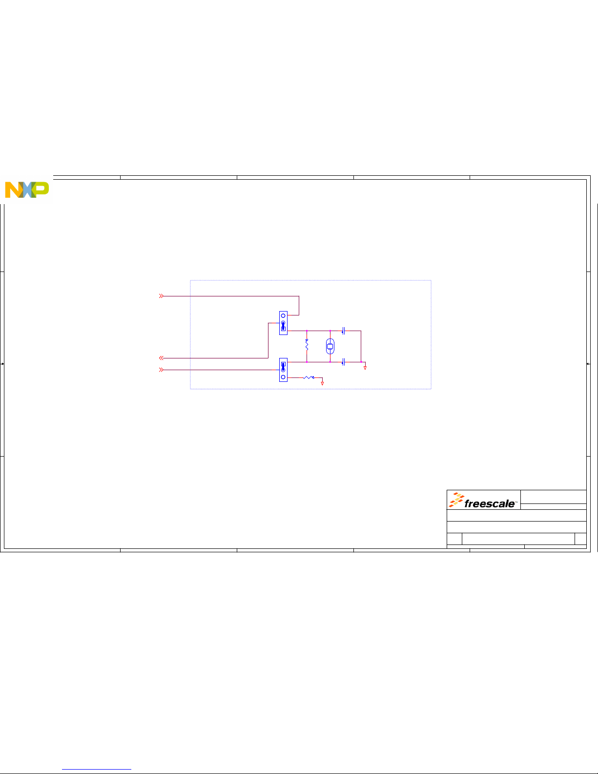
5
5
4
4
3
3
2
2
1
1
D D
C C
B B
A A
Oscillators and External Clock
NX8045GB-40.000M-STD-CSJ-1 XTAL
(Optimised for Automotive, 8pF Load capacitance)
(From SMA connector on main board)
Clocks
(Note the 32KHz osc
pins are not bonded
out on the 100 pin
package)
EXTAL
MCU-XTAL
MCU-EXTAL
XTAL
EXT-CLK
GND
GND
MCU-XTAL
4
MCU-EXTAL4
EXT-CLK
8
Drawing Title:
Size Document Number Rev
Date: Sheet
of
Page Title:
Automotive Microcontroller
Applications
East Kilbride, Scotland
SCH-28701 PDF: SPF-28701 A1
MPC5746C 100 BGA Daughter Card
B
Tuesday, August 18, 2015
Clocks
68
Freescale General Business Use
Drawing Title:
Size Document Number Rev
Date: Sheet of
Page Title:
Automotive Microcontroller
Applications
East Kilbride, Scotland
SCH-28701 PDF: SPF-28701 A1
MPC5746C 100 BGA Daughter Card
B
Tuesday, August 18, 2015
Clocks
68
Freescale General Business Use
Drawing Title:
Size Document Number Rev
Date: Sheet of
Page Title:
Automotive Microcontroller
Applications
East Kilbride, Scotland
SCH-28701 PDF: SPF-28701 A1
MPC5746C 100 BGA Daughter Card
B
Tuesday, August 18, 2015
Clocks
68
Freescale General Business Use
J1
1
2
3
C7
12PF
R34 0
DNP
Y1
40.0MHZ
12
R8
1.0M
DNP
J2
1
2
3
C6
12PF
Page 86
5
5
4
4
3
3
2
2
1
1
D D
C C
B B
A A
Place resistors as close as possible to MCU
Ethernet Termination
High Speed Signal Termination
PH2
PH1
PG12
PH0
PG13
PH2-R
PH1-R
PH0-R
PG13-R
PG12-R
PG0-RPG0
PG13
4
PG12
4
PH0
4
PH1
4
PH2
4
PG13-R
8
PG12-R
8
PH0-R
8
PH1-R
8
PH2-R
8
PG0-R
8
PG0
4
Drawing Title:
Size Document Number Rev
Date: Sheet
of
Page Title:
Automotive Microcontroller
Applications
East Kilbride, Scotland
SCH-28701 PDF: SPF-28701 A1
MPC5746C 100 BGA Daughter Card
B
Tuesday, August 18, 2015
High Speed Signal Termination
78
Freescale General Business Use
Drawing Title:
Size Document Number Rev
Date: Sheet of
Page Title:
Automotive Microcontroller
Applications
East Kilbride, Scotland
SCH-28701 PDF: SPF-28701 A1
MPC5746C 100 BGA Daughter Card
B
Tuesday, August 18, 2015
High Speed Signal Termination
78
Freescale General Business Use
Drawing Title:
Size Document Number Rev
Date: Sheet of
Page Title:
Automotive Microcontroller
Applications
East Kilbride, Scotland
SCH-28701 PDF: SPF-28701 A1
MPC5746C 100 BGA Daughter Card
B
Tuesday, August 18, 2015
High Speed Signal Termination
78
Freescale General Business Use
R1 50
R4 50
R2 50
R5 50
R6 50
R3 50
Page 87
5
5
4
4
3
3
2
2
1
1
D D
C C
B B
A A
Daughter Card Connectors (Plugs)
Notes:
- there was no neat way to fit these connectors onto a B sized sheet so unfortunately the sheet
size has been increased to C so will need to be printed on larger paper.
- The Crystal Signals are NOT routed via the daughtercard connectors
- The Specific MCU power pins are not routed via the daughter card however the jumpered MCU
supply lines are brought up from the main board (see the top pins of the connector on the left)
- The connector schematic symbols have been horizontally mirrored so they match the main EVB
connector. This has no bearing on the PCB placement or footprint. Pin1 on the recepticle mates
with pin 1 on the plug.
Connectors on Main board (Shown for reference)
(PO12)
(PO3)
(PO2)
(PO7)
(PN12)
(PO10)
(PN8)
(PO4)
(PN7)
(PO9)
(PN4)
(PO14)
(PN5)
(PP0)
(PN2)
(PO5)
(PN14)
(PN13)
(PN11)
(PN9)
(PN10)
(GND)
(GND)
(GND)
(GND)
(GND)
(GND)
(GND)
(GND)
(GND)
(GND)
(GND)
(GND)
(GND)
(GND)
(GND)
(GND)
(GND)
(GND)
(GND)
(GND)
(GND)
(GND)
Plug
(GND)
(GND)
(GND)
(GND)
(GND)
(GND)
(GND)
(GND)
(GND)
(GND)
(GND)
(GND)
(GND)
(GND)
(GND)
(GND)
(GND)
(GND)
(GND)
(GND)
(GND)
(GND)
(GND)
(GND)
(GND)
(GND)
(GND)
(GND)
(GND)
(GND)
(PN3)
(PN6)
(PN0)
(PP8)
(PP11)
(PP3)(PP10)
(PP4)
(PP5)
(PO11)
(PP2)
(PO8)
(PP7)
(PO13)
(PP6)
(PO15)
(PP1)
(PO6)
(PP9)
(PN15)
(PL11)
(PL6)
(PL7)
(PL15)
(PM1)
(PM2)
(PL4)
(PL8)
(PL10)
(PL5)
(PL13)
(PM0)
(PL14)
(PM9)
(PM7)
(PM10)(PM8)
(PM6)
(PM13)
(PN1)
(PM11)
(PL2)
(PM15)
(PM12)
(PL9)
(PL3)
(PL12)
(GND)
(GND)
(GND)
(GND)
(GND)
(GND)
(GND)
(GND)
(GND)
(GND)
(GND)
(GND)
(GND)
(GND)
(GND)
(GND)
(GND)
(GND)
(GND)
(GND)
(GND)
Plug
(GND)
(GND)
(GND)
(GND)
(GND)
(GND)
(GND)
(GND)
(GND)
(GND)
(GND)
(GND)
(GND)
(GND)
(GND)
(GND)
(GND)
(GND)
(GND)
(GND)
(GND)
(GND)
(GND)(GND)
(PB2)
(PE6)
(PC13)
(PK10)
(PC8)
(PK13)
(PK15)
(PC15)
(PG5)
(PD0)
(PI7)
(PE1)
(PI6)
(PE11)
(PG9)
(PG8)
(PK2)
(PF13)
(PK4)
(PK6)
(PK8)
(PJ11)
(PJ10)
(PK0)
(PJ9)
(PH7)
(PH6)
(PB3)
(PH8)
(PE7)
(PK9)
(PC12)
(PK11)
(PK14)
(PK12)
(PC9)
(PL0)
(PC14)
(PJ4)
(PH14)
(PO1)
(PH13)
(PG4)
(PH15)
(PE10)
(PE0)
(PK1)
(PF12)
(PK3)
(PK5)
(PF11)
(PK7)
(PC6)
(PC7)
(PJ12)
(PJ15)
(PF1)
(PH4)
(PE5)
(PI5)
(PQ0)
(PC4)
(PC2)
(PH11)
(PE14)
(PQ4)
(PQ5)
(PQ7)
(PP15)
(PE12)
(PH3)
(PM3)
(PM14)
(PD12)
(PI11)
(PD10)
(MLB_DAT)
(MLB_SIG)
(MLB_CLK)
(MLB_SN)
(MLB_SP_
(MLB_SP)
(PD7)
(PJ5)
(PD5)
(PB5)
(PB11)
(PD8)
(PI9)
(PB4)
(PJ3)
(PF2)
(PH5)
(PQ3)
(PC3)
(PE4)
(PQ1)
(PG10)
(PQ2)
(PQ6)
(PP13)
(PP12)
(PI4)
(PP14)
(PM4)
(PL1)
(PM5)
(PI13)
(PB12)
(PD9)
(PI12)
(PB7)
(PI15)
(MLB_CN)
(MLB_CP)
(MLB_DN)
(MLB_DP)
(PJ7)
(PD11)
(PJ6)
(PD6)
(PD2)
(PD3)
(PJ8)
(PB6)
(PD0)
(PI10)
(PD4)
(PF6)
(PF4)
(PF7)
(PF3)
PG3
PE8
PA0
MCU_5V0_S
MCU_1V25_L
PB10
PA15
PA4
PJ13
PF9
PA14
PI3
PI1
PI2
PI0
EXT-CLK
PA12
PF0
PA13
PG2
PA2
PE9
PA1
MCU-RSTx
PF8
PG6
PC11
PB0
MCU_3V3_S
PG7
PC10
PB1
PF10
PJ14
MCU_3V3_L
MCU_5V0_L
PC0
PG14
PC5
PA7
PG1
PF15
PE13
PA11
PH1-R
PH0-R
PA3
PH10
PH12
PG15
PA6
PA5
PF5
PJ2
PJ0
PJ1
PD1
PD13
DC_5V0_S
DC_P12V
DC_1V25_L
PA8
PH2-R
PG0-R
PF14
PA9
PA10
PG12-R
PG13-R
PC1
PE3
PE15
PG11
PORSTx
PE2
PI14
DC_3V3_S
DC_5V0_L
DC_3V3_L
PH9
GND GND
GND GND
PG2
4
PA2
4
PE9
4
PA1
4
MCU-RSTx
4
MCU_5V0_S
2
MCU_1V25_L
2
MCU_3V3_S
2
MCU_3V3_L
2
MCU_5V0_L
2
PG6
4
PC11
4
PB0
4
PF8
4
PF10
4
PJ14
5
PA13
4
PA12
4
PF0
4
PI3
5
PI1
5
PI2
5
PI0
5
PG3
4
PE8
4
PA0
4
PG7
4
PC104
PB1
4
PF9
4
PA14
4
PJ13
5
PA4
4
PA15
4
PB10
4
EXT-CLK
6
PH10
4
PC5
4
PG14
4
PH12
4
PA6
4
PA5
4
PG15
4
PA11
4
PA7
4
PE13
4
PF15
4
PG1
4
PH1-R
7
PH0-R
7
PA3
4
PD13
4
PJ0
5
PD1
4
PJ1
5
PF5
4
PJ2
5
PC0
4
PC1
4
PE3
4
PE15
4
PORSTx
4
PE2
4
PG11
4
PA10
4
PA9
4
PA8
4
PF14
4
PG0-R
7
PH2-R
7
PG12-R
7
PG13-R
7
PH9
4
PI14
5
Drawing Title:
Size Document Number Rev
Date: Sheet
of
Page Title:
Automotive Microcontroller
Applications
East Kilbride, Scotland
SCH-28701 PDF: SPF-28701 A1
MPC5746C 100 BGA Daughter Card
C
Tuesday, August 18, 2015
Daughter Card Connectors (Plugs)
88
Freescale General Business Use
Drawing Title:
Size Document Number Rev
Date: Sheet of
Page Title:
Automotive Microcontroller
Applications
East Kilbride, Scotland
SCH-28701 PDF: SPF-28701 A1
MPC5746C 100 BGA Daughter Card
C
Tuesday, August 18, 2015
Daughter Card Connectors (Plugs)
88
Freescale General Business Use
Drawing Title:
Size Document Number Rev
Date: Sheet of
Page Title:
Automotive Microcontroller
Applications
East Kilbride, Scotland
SCH-28701 PDF: SPF-28701 A1
MPC5746C 100 BGA Daughter Card
C
Tuesday, August 18, 2015
Daughter Card Connectors (Plugs)
88
Freescale General Business Use
TPV6TPV2
TPV1
TPV3
P20
PLUG 180
2
SH1SH2
SH5SH6
1
43
65
87
109
1211
1413
1615
1817
2019
2221
2423
2625
2827
3029
3231
3433
3635
3837
4039
4241
4443
4645
4847
5049
5251
5453
5655
5857
6059
SH3SH4
6261
6463
6665
6867
7069
7271
7473
7675
7877
8079
8281
8483
8685
8887
9089
9291
9493
9695
9897
10099
102101
104103
106105
108107
110109
112111
114113
116115
118117
120119
SH7SH8
SH9SH10
122121
124123
126125
128127
130129
132131
134133
136135
138137
140139
142141
144143
146145
148147
150149
152151
154153
156155
158157
160159
162161
164163
166165
168167
170169
172171
174173
176175
178177
180179
SH11SH12
TPV4
TPV5
P21
PLUG 180
2
SH1SH2
SH5SH6
1
43
65
87
109
1211
1413
1615
1817
2019
2221
2423
2625
2827
3029
3231
3433
3635
3837
4039
4241
4443
4645
4847
5049
5251
5453
5655
5857
6059
SH3SH4
6261
6463
6665
6867
7069
7271
7473
7675
7877
8079
8281
8483
8685
8887
9089
9291
9493
9695
9897
10099
102101
104103
106105
108107
110109
112111
114113
116115
118117
120119
SH7SH8
SH9SH10
122121
124123
126125
128127
130129
132131
134133
136135
138137
140139
142141
144143
146145
148147
150149
152151
154153
156155
158157
160159
162161
164163
166165
168167
170169
172171
174173
176175
178177
180179
SH11SH12
Page 88

Document Number: MPC5748GEVBUG
Rev. 0
08/2015
How to Reach Us:
Home Page:
freescale.com
Web Support:
freescale.com/support
Information in this document is provided solely to enable system and software
implementers to use Freescale products. There are no express or implied copyright
licenses granted hereunder to design or fabricate any integrated circuits based on the
information in this document. Freescale reserves the right to make changes without
further notice to any products herein.
Freescale makes no warranty, representation, or guarantee regarding the suitability
of its products for any particular purpose, nor does Freescale assume any liability
arising out of the application or use of any product or circuit, and specifically
disclaims any and all liability, including without limitation consequential or
incidental damages. “Typical” parameters that may be provided in Freescale data
sheets and/or specifications can and do vary in different applications, and actual
performance may vary over time. All operating parameters, including “typicals,”
must be validated for each customer application by customer's technical experts.
Freescale does not convey any license under its patent rights nor the rights of others.
Freescale sells products pursuant to standard terms and conditions of sale, which can
be found at the following address: freescale.com/SalesTermsandConditions.
Freescale and the Freescale logo are trademarks of Freescale Semiconductor, Inc.,
Reg. U.S. Pat. & Tm. Off. All other product or service names are the property of
their respective owners. The Power Architecture and Power.org word marks and the
Power and Power.org logos and related marks are trademarks and service marks
licensed by Power.org.
© 2015 Freescale Semiconductor, Inc.
 Loading...