

Page 1
Msgapps1
ps
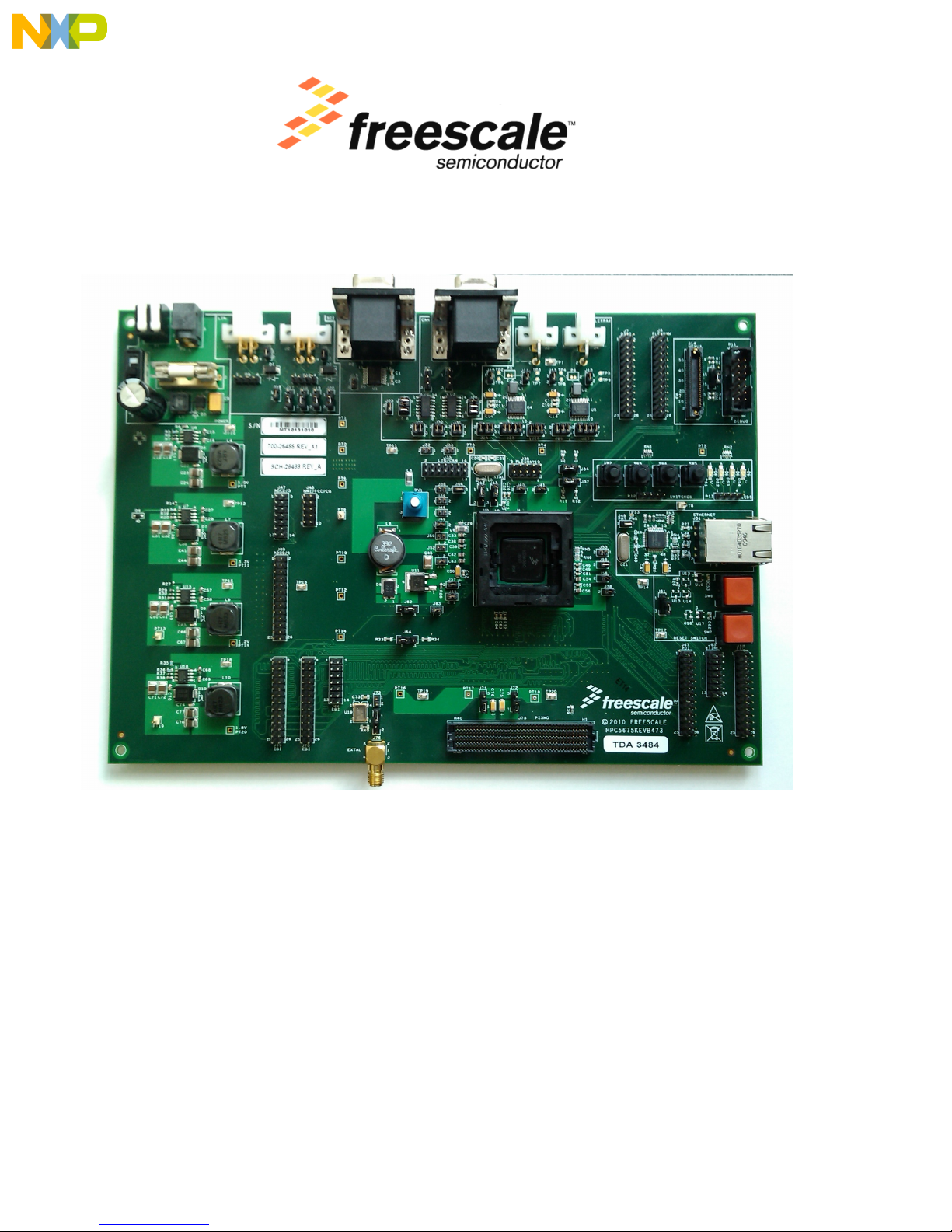
MPC5675EVB Users Manual
473 BGA Rev B
Revision 2.0
August 2010
Page 2

MPC5675EVB Users Manual Rev 2.0 July 2010
Revision
Date
Author
Comment
0.1 April 2010 A.
Robertson
Initial Release, RevA PCB’s only
.
1.2 May 2010
A. Robertson
Updated with known bugs list
Revision History:
2.0 July 2010 A. Robertson Updated for new EVB Rev B
Information in this document is provided solely to enable system and software implementers to use
Freescale Semiconductor products. There are no express or implied copyright licenses granted
hereunder to design or fabricate any integrated circuits or integrated circuits based on the information
in this document. Freescale Semiconductor reserves the right to make changes without further notice
to any products herein. Freescale Semiconductor makes no warranty, representation or guarantee
regarding the suitability of its products for any particular purpose, nor does Freescale Semiconductor
assume any liability arising out of the application or use of any product or circuit, and specifically
disclaims any and all liability, including without limitation consequential or incidental damages.
“Typical” parameters that may be provided in Freescale Semiconductor data sheets and/or
specifications can and do vary in different applications and actual performance may vary over time. All
operating parameters, including “Typicals”, must be validated for each customer application by
customer’s technical experts. Freescale Semiconductor does not convey any license under its patent
rights nor the rights of others. Freescale Semiconductor products are not designed, intended, or
authorized for use as components in systems intended for surgical implant into the body, or other
applications intended to support or sustain life, or for any other application in which the failure of the
Freescale Semiconductor product could create a situation where personal injury or death may occur.
Should Buyer purchase or use Freescale Semiconductor products for any such unintended or
unauthorized application, Buyer shall indemnify and hold Freescale Semiconductor and its officers,
employees, subsidiaries, affiliates, and distributors harmless against all claims, costs, damages, and
expenses, and reasonable attorney fees arising out of, directly or indirectly, any claim of personal
injury or death associated with such unintended or unauthorized use, even if such claim alleges that
Freescale Semiconductor was negligent regarding the design or manufacture of the part.
Learn More: For more information about Freescale products, please visit www.freescale.com
Freescale™ and the Freescale logo are trademarks of Freescale Semiconductor.
All other product or service names are the property of their respective owners.
© Freescale Semiconductor, 2010; All Rights Reserved
MPC5675EVB i
Page 3

MPC5675EVB Users Manual Rev 2.0 July 2010
INDEX
1. INTRODUCTION ...................................................................................................................................................... 1
2. EVB FEATURES ...................................................................................................................................................... 2
3. CONFIGURATION ................................................................................................................................................... 1
3.1 P
3.2 MCU C
3.3 ONCE
3.4 CAN C
3.5 RS232 C
LIN C
3.6 F
3.7 E
3.8 PISMO DRAMC C
4. DEFAULT JUMPER SUMMARY TABLE .......................................................................................................... 14
OWER SUPPLY CONFIGURATION
3.1.1 Power Supply Connectors ........................................................................................................................ 1
3.1.2 Power Switch (SW1) .................................................................................................................................. 1
3.1.3 Power Status LED’s and Fuse ................................................................................................................. 2
3.1.4 MCU Supply Routing and Jumpers (J78, J79) ..................................................................................... 2
LOCK CONTROL
3.2.1 Main Clock Selection (J42, J43, J73 and J74) ....................................................................................... 4
3.2.2 Reset Boot Configuration (J69, J34, J37) ............................................................................................... 5
AND NEXUS
3.3.1 Debug Connector Pinouts ......................................................................................................................... 5
ONFIGURATION
ONFIGURATION
ONFIGURATION
LEX
THERNET
(J5, J6, J16, J23,J18,J17,J19,J20) .......................................................................................... 9
RAY C
ONFIGURATION
....................................................................................................................................................... 12
..................................................................................................................................... 4
............................................................................................................................................ 5
(J21, J22, J29, J30, J31) ........................................................................................... 7
(J5,J6,J15, J16, J23) .............................................................................................. 8
ONNECTOR
..................................................................................................................... 1
(J19, J27, J25, J26, J28) ................................................................................ 10
....................................................................................................................... 13
5. USER CONNECTOR DESCRIPTIONS .............................................................................................................. 16
5.1.1 eTimer (Connector J65) ......................................................................................................................... 16
5.1.2 ADC 0/1 (Connector J60) ........................................................................................................................ 16
5.1.3 ADC 2/3 (Connector J47) ........................................................................................................................ 17
5.1.4 EBI (Connector J66, J69, J70) ............................................................................................................... 17
5.1.5 NMI / FCC / CG (J45) ............................................................................................................................. 18
5.1.6 PDI (J67) .................................................................................................................................................. 18
5.1.7 FLEXPWM (J8) ........................................................................................................................................ 19
5.1.8 FEC (J68) ................................................................................................................................................. 19
5.1.9 FLEXRAY (J36) ....................................................................................................................................... 19
5.1.10 LINFLEX / FLEXCAN (J35) ............................................................................................................... 20
5.1.11 DSPI (J7) .............................................................................................................................................. 20
6. KNOWN BUGS LIST ............................................................................................................................................. 21
APPENDIX A - SCHEMATICS
MPC5675EVB ii
Page 4

MPC5675EVB Users Manual Rev 2.0 July 2010
Index of Figures and Tables
F
IGURE
3-1
EV ................................................................................................................................................................... 1
F
IGURE
3-2
2.1
F
IGURE
F
IGURE
F
IGURE
F
IGURE
F
IGURE
F
IGURE
T
ABLE
T
ABLE
T
ABLE
T
ABLE
T
ABLE
T
ABLE
T
ABLE
T
ABLE
T
ABLE
T
ABLE
T
ABLE
T
ABLE
T
ABLE
T
ABLE
T
ABLE
T
ABLE
T
ABLE
T
ABLE
T
ABLE
T
ABLE
T
ABLE
T
ABLE
T
ABLE
T
ABLE
T
ABLE
T
ABLE
MM POWER CONNECTOR
3-3
2-L
EVER POWER CONNECTOR
3-5
EVB C
LOCK SELECTION
3-7.
MPC5675 JTAG / ONCE C
3-8
CAN P
HYSICAL INTERFACE CONNECTOR
3-9
RS232 P
3-10
LIN P
3-1
MCU P
3-2
CLOCK SOURCE JUMPER SELECTION
3-6
BOOTCFG C
3-9.
NEXUS D
3-10
CAN C
3-11
RS232 C
3-12
LIN C
3-13
FLEXRAY
3-14
FLEXRAY POWER CONTROL JUMPERS
3-15
FLEXRAY CONTROL JUMPERS
3-16
PULL UP/ PULL DOWN RESISTORS FOR ETHERNET PHYSICAL
3-17
EHTERNET PHYSICAL INTERFACE POWER SUPPLY ENABLED
4-1
DEFAULT JUMPER POSITIONS
5-1
ETIMER CONNECTOR PINOUT
5-2
ADC 0/1 C
5-3
ADC 2/3 C
5-4
EBI C
5-5
EBI C
5-6
EBI C
5-7
NMI / FCC / CG C
5-8
PDI C
5-9
FLEXPWM C
5-10
FEC C
5-11
FLEXRAY C
5-12
LIN / CAN C
5-13
DSPI C
HYSICAL INTERFACE CONNECTOR
HYSICAL INTERFACE CONNECTORS
OWER SUPPLY JUMPERS
ONTROL
EBUG CONNECTOR PINOUT
ONTROL JUMPERS
ONTROL JUMPERS
ONTROL JUMPERS
MCU S
IGNAL ROUTING JUMPERS
ONNECTOR PINOUT
ONNECTOR PINOUT
ONNECTOR PINOUT
ONNECTOR PINOUT
ONNECTOR PINOUT
ONNECTOR PINOUT
ONNECTOR PINOUT
ONNECTOR PINOUT
ONNECTOR PINOUT
ONNECTOR PINOUT
ONNECTOR PINOUT
ONNECTOR PINOUT
.......................................................................................................................... 1
....................................................................................................................... 1
................................................................................................................................. 4
ONNECTOR
...................................................................................................... 5
...................................................................................................... 7
.................................................................................................. 8
.................................................................................................... 9
..................................................................................................................... 3
.............................................................................................................. 4
...................................................................................................................................... 5
........................................................................................................... 6
(J30, J31, J21, J22) ........................................................................................... 7
.......................................................................................................................... 8
............................................................................................................................... 9
(J19, J27) ........................................................................... 10
(J25) ............................................................................................. 10
(J26, J28) .................................................................................................. 11
................................................................... 12
(J48) ......................................................... 12
........................................................................................................................ 14
(J65) ................................................................................................................. 16
(J60) ............................................................................................................ 16
(J47) ............................................................................................................ 17
(J66) ..................................................................................................................... 17
(J69) ..................................................................................................................... 17
(J70) ..................................................................................................................... 17
(J45) ............................................................................................... 18
(J67) .................................................................................................................... 18
(J8) .......................................................................................................... 19
(J68) ................................................................................................................. 19
(J36) ....................................................................................................... 19
(J35) ....................................................................................................... 20
(J7) .................................................................................................................. 20
MPC5675EVB iii
Page 5

MPC5675EVB Users Manual Rev 2.0 July 2010
1. Introduction
This user’s manual details the setup and configuration of the Freescale Semiconductor MPC5675K
Evaluation Board (hereafter referred to as the EVB). The EVB is intended to provide a mechanism for
easy customer evaluation of the MPC5675K family of microprocessors, and to facilitate hardware and
software development.
At the time of writing this document, the MPC5675K family is offered in a 257MAPBGA and
473MAPBGA package. Both the 473MAPBGA and 257BGA packages support Nexus debug for
development purposes. For the latest product information, please speak to your Freescale
representative or consult the MPC5675K web pages at www.freescale.com
The EVB is intended for bench / laboratory use and has been designed using normal temperature
specified components (+70°C).
This manual is written for the 473BGA, jumper numbers change between Rev_A and Rev_B so
please check correct schematic and EVB.
MPC5675EVB Page 1 of 29
Page 6

MPC5675EVB Users Manual Rev 2.0 July 2010
IMPORTANT
2. EVB Features
The EVB provides the following key features:
• MCU Socket supporting the 473 BGA production package.
• Single 12V external power supply input with on-board regulators to provide all of the
necessary EVB and MCU voltages. Power may be supplied to the EVB via a 2.1mm barrel
style power jack or a 2-way level connector. 12V operation allows in-car use if desired.
• Flexible on-board power supply configuration with the option to bypass the internal MCU
regulators if desired.
• Master power switch and regulator status LED’s
• User reset switch with reset status LED’s
• Control of the BOOTCFG status via a dedicated jumper.
• Flexible MCU clocking options:
40MHz Oscillator Crystal
SMA connector to allow external clock support
8Mhz Oscillator circuit.
• SMA connector on MCU-CLKOUT signal for easy access.
• Standard 14-pin ONCE JTAG debug connector and the new 50-pin Samtec ERF8 NEXUS
connectors for 16MDO channels.
• All MCU signals are accessible on port-ordered groups of 0.1” pitch headers.
• SCI channels A and B can be routed to a standard DB9 female connector (PC RS-232
compliant) via a Maxim physical interface.
• FlexCAN channels A and B can be routed to 0.1” headers and DB9 connector via a NXP high
speed CAN transceiver which supports both 3.3V and 5V inputs.
• FlexCAN channels are routed to the prototyping area with DB9 connectors to allow additions
CAN physical interfaces to be easily integrated.
• User prototyping area consisting of a 0,1” grid of through hole pads with easy access to the
EVB ground and power supply rails.
• Ethernet signals routed to a National Semiconductor physical interface and Pulsejack RJ45
connector with integrated magnetics.
• LINFLEX Molex Connector and 0.1” 4 pin header are available.
• FLEXRAY CON PLUG Connector is available.
• A PISMO connector is available for DDR memory types from Micron
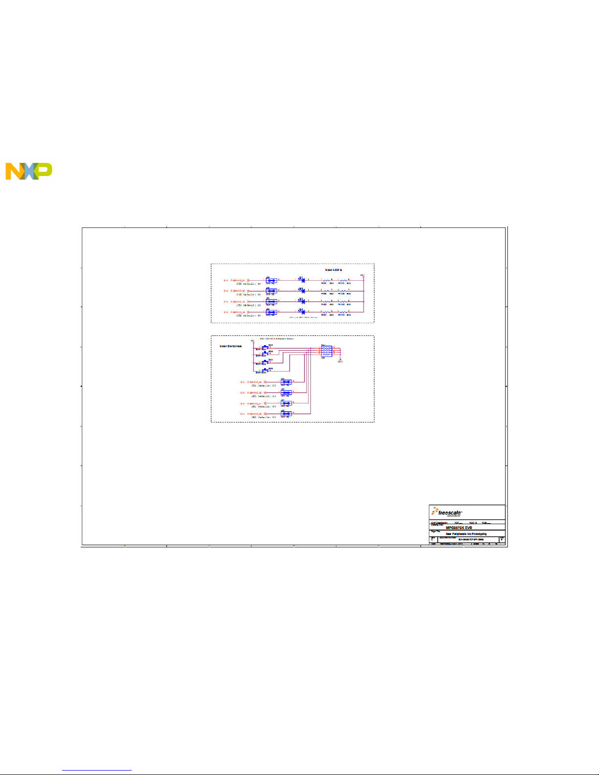
• 4 active low LED’s and 4 pushbutton switches for development purposes.
• Jumper selectable variable resistor connected to ADC channel 0, driving between VRH and
VRL.
• Liberal scattering of GND test points (surface mount loops) placed throughout the EVB.
Before the EVB is used or power is applied, please fully read the following
sections on how to correctly configure the board.
Failure to correctly configure the board may cause irreparable component, MCU or EVB
damage.
MPC5675EVB Page 2 of 29
Page 7
MPC5675EVB Users Manual Rev 2.0 July 2010
Power Regulators
Ethernet
Reset
User SW & LEDs
JTAG / Nexus
DSPI & FlexPWM
FlexRay
FlexCAN
SCI
LinFlex
PDI, eTimer & FEC
ADC
EBI
NMI/FCCU/CG
MCU
Power Switch
3. Configuration
This section details the configuration of each of the EVB functional blocks.
Throughout this document, all of the default jumper and switch settings are clearly marked with “(D)” and are shown in blue text.
This should allow a more rapid return to the default state of the EVB if required. Note that the default configuration for 3-way
jumpers is a header fitted between pins 1 and 2. On the EVB, 2-way and 3-way jumpers have been aligned such that Pin 1 is
either to the top or to the left of the jumper. On 2-way jumpers, the source of the signal is connected to Pin 1.
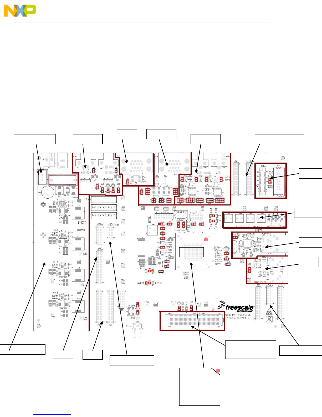
The EVB has been designed with ease of use in mind and has been segmented into functional blocks as shown below.
Detailed silkscreen legend has been used throughout the board to identify all switches, jumpers and user connectors.
Figure 3-1 EV
PISMO DDR
(473BGA ONLY)
PIN 1
MCU
Page 8
MPC5675EVB Users Manual Rev 2.0 July 2010
3.1 Power Supply Configuration
The EVB requires an external power supply voltage of 12V DC, minimum 1A. This allows the EVB to
be easily used in a vehicle if required. The single input voltage is regulated on-board using switching
regulators to provide the necessary EVB and MCU operating voltages of 5.0V, 3.3V 1.8v and 1.2V
(257BGA does not have the 1.8v supply). For flexibility there are two different power supply input
connectors on the EVB as detailed below.
3.1.1 Power Supply Connectors
2.1mm Barrel Connector – P4:
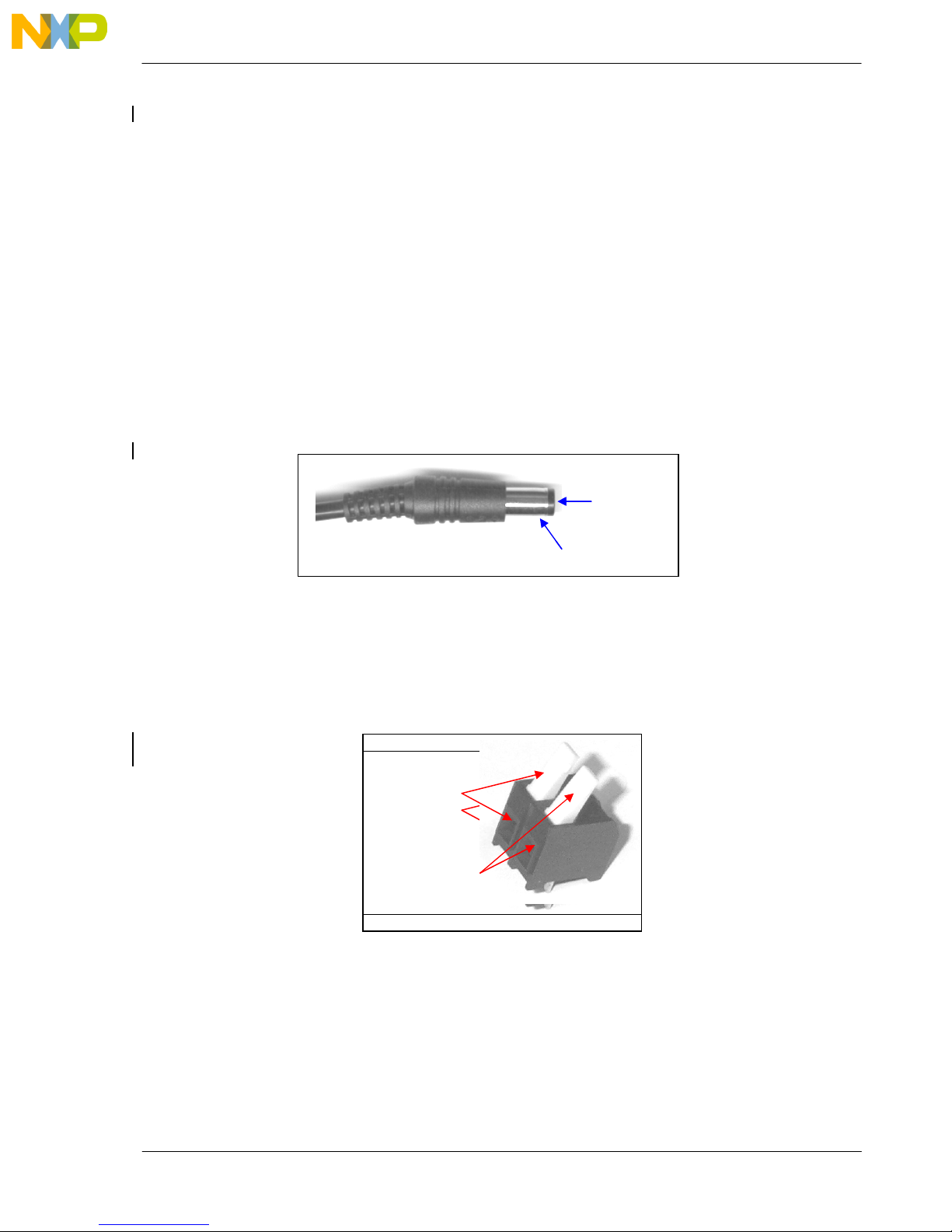
This connector should be used to connect the supplied wall-plug mains adapter. Note – if a
replacement or alternative adapter is used, care must be taken to ensure the 2.1mm plug uses the
correct polarisation as shown below:
Figure 3-2 2.1mm Power Connector
2-Way Lever Connector – P1:
This can be used to connect a bare wire lead to the EVB, typically from a laboratory power supply.
The polarisation of the connectors is clearly marked on the EVB. Care must be taken to ensure
correct connection.
V+ (12V)
V+ (12V)
GND
GND
Figure 3-3 2-Lever Power Connector
GND
GND
V+ (12V)
V+ (12V)
3.1.2 Power Switch (SW1)
Slide switch SW1 can be used to isolate the power supply input from the EVB voltage regulators if
required.
Position 1 will turn the EVB OFF
Position 2 will turn the EVB ON
MPC5675EVB Page 1 of 29
Page 9
MPC5675EVB Users Manual Rev 2.0 July 2010
3.1.3 Power Status LED’s and Fuse
When power is applied to the EVB, a green power LED’s adjacent to the voltage regulators show the
presence of the 12v supply voltages.
If there is no power to the MCU it is possible that either power switch SW1 is in the “OFF” position or
that the fuse F1 has blown. The fuse will blow if power is applied to the EVB in reverse-bias, where a
protection diode ensures that the main fuse blows rather than causing damage to the EVB circuitry. If
the fuse has blown, check the bias of your power supply connection then replace fuse F1 with a
20mm 500mA fast blow fuse.
3.1.4 MCU Supply Routing and Jumpers
(J78, J79)
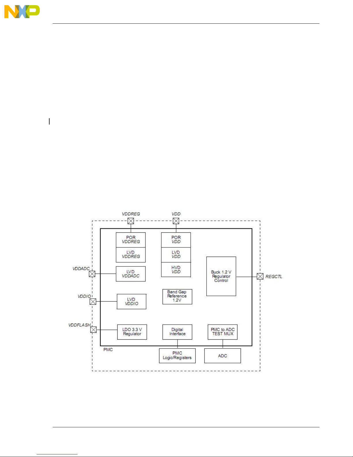
The EVB is designed to run the MCU at 3.3v with the option to run the ADC and the ballast circuitry at
5v.
The MCUs ADC and ballast circuitry can be operated in 5v and 3.3v modes by changing J78 (ADC)
and J79 (PMU) to the 3.3v or 5V jumper position.
The FLEXCAN and FlexRay circuitry also has 5V supplies to the transceivers.
MPC5675EVB Page 2 of 29
Page 10

MPC5675EVB Users Manual Rev 2.0 July 2010
J41
(D)
(D)
(D)
J55
(D)
(D)
J40
(D)
J44
(D)
J78
(D)
(D)
J79
(D)
J59
J57
Table 3-1 MCU Power Supply Jumpers
Power
Jumper Position Description
Domain
3.3V
3.3v/1.8v
GND
3.3v
3.3v
3.3v
3.3v
3.3v/5.0v
1.2v
(VDD_HV_IO)
J63
(VDD_HV_DRAM)
J58
(VDD_DRAM_VTT)
(VDD_HV_FLA)
J56
(VDD_HV_PDI)
(VDD_HV_OSC)
(VDD_HV_ADV)
(VDD_HV_ADR)
J46
(VDD_LV_COR)
1-2
3.3 V to supply HV_DRAM with 1.8v option
Position 2 External supplies can be added to pin 2 if extra
1-2
1-2
1-2
1-2
1-2
1-2
1-2
Supplies the core with 1.2v in external mode
This supplies the IO with 3.3v
DRAM voltages are required.
Grounded for Mobile DDR termination
External supplies can be added to pin 2 if extra
DRAM voltages are required
3.3v supply to HV_FLA
3.3v to supply PDI
External supplies can be added to pin 2 if extra
PDI voltages are required.
3.3v to Oscillator circuitry
3.3v to ADC circuitry
ADC Reference voltage 3.3v
ADC Reference voltage 5.0v
ONLY. Do not populate if generating core
voltage from internal VREG. This may damage
1-2
the device.
3.3v/5.0v
1.2v
3.3v/5.0v
(VDD_HV_PMU)
1-2 This should always be populated
(VREG_CTRL)
1-2 This should always be populated
(PMU)
3.3v supply for the PMU(VREG).
5.0v supply for the PMU(VREG).
2-3
The jumper configuration shown in Table 3-1, details the default state (D) of the EVB. In this
configuration all power is supplied from the regulators.
MPC5675EVB Page 3 of 29
Page 11
MPC5675EVB Users Manual Rev 2.0 July 2010
Jumper
Position
PCB
Description
(D)
(D)
(D)
(D)
MCU
3.2 MCU Clock Control
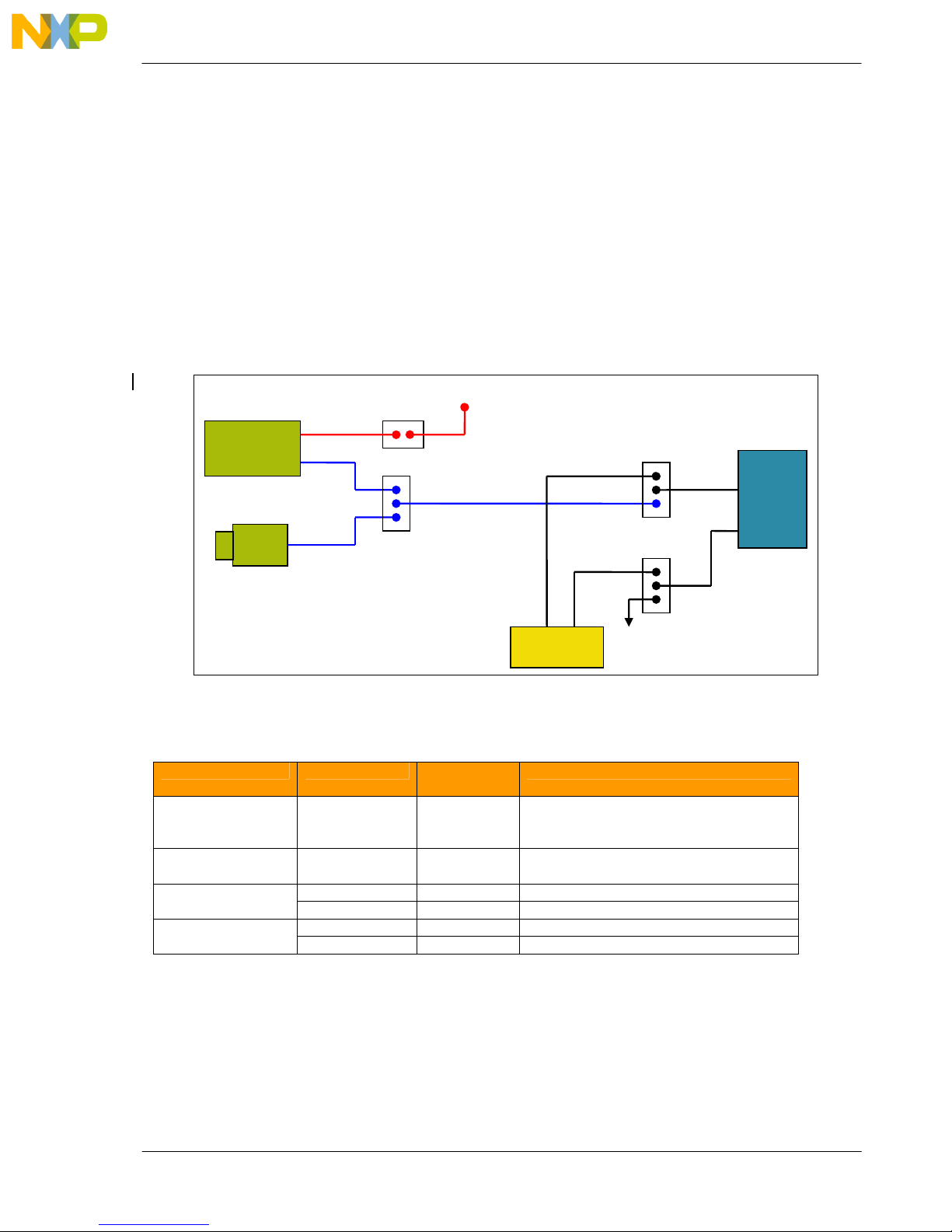
3.2.1 Main Clock Selection (J42, J43, J73 and J74)
The EVB supports three possible MCU clock sources:
(1) The local 40MHz oscillator circuit
(2) An 4MHz oscillator module on the EVB (U19), driving the MCU EXTAL signal
(3) An external clock input to the EVB via the SMA connector (J76), driving the MCU EXTAL
signal
The clock circuitry is shown in the diagram below. Please refer to the appropriate EVB schematic for
specific jumper numbers and circuitry.
Oscillator
Module
(U19)
J73
J74
SMA
(J76)
Figure 3-4 EVB Clock Selection
Table 3-2 Clock Source Jumper Selection
3.3V
Local Crystal
Circuit (Y1)
1
1
GND
EVB Clock Circuitry
J43
EXTAL
XTAL
J42
FITTED
J73 (U19 PWR)
J74 (OSC SEL)
J42
Must Match J43
J43
Must Match J42
REMOVED
1-2
2-3
1-2
2-3 GND GND
1-2
2-3 EVB MCU Clock is Selected by J74
Note that the 3.3V regulator must be enabled when using oscillator module Y1.
The MPC5675K clock circuitry is all 3.3v based. Any external clock signal driven into the SMA
MPC5675EVB Page 4 of 29
Legend
EVB oscillator module U19 is powered
MOD 8Mhz Oscillator is routed from U19
SMA
Y1 MCU Clock is Y1 XTALIN
Y1 MCU Clock is Y1 XTALOUT
CAUTION
EVB oscillator module U19 is not
powered
SMA external square wave input
connector must have a maximum voltage of 3.3V.
Page 12
MPC5675EVB Users Manual Rev 2.0 July 2010
J64 (FAB)
J37 (ABS2)
J34 (ABS0)
Boot ID
Boot Mode
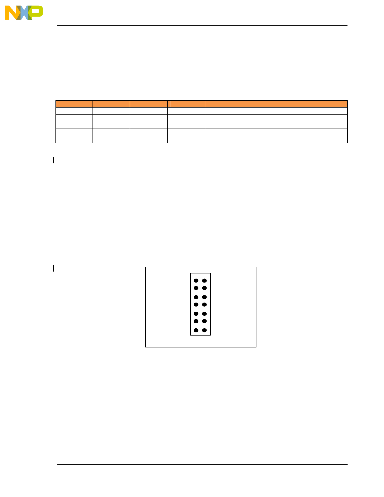
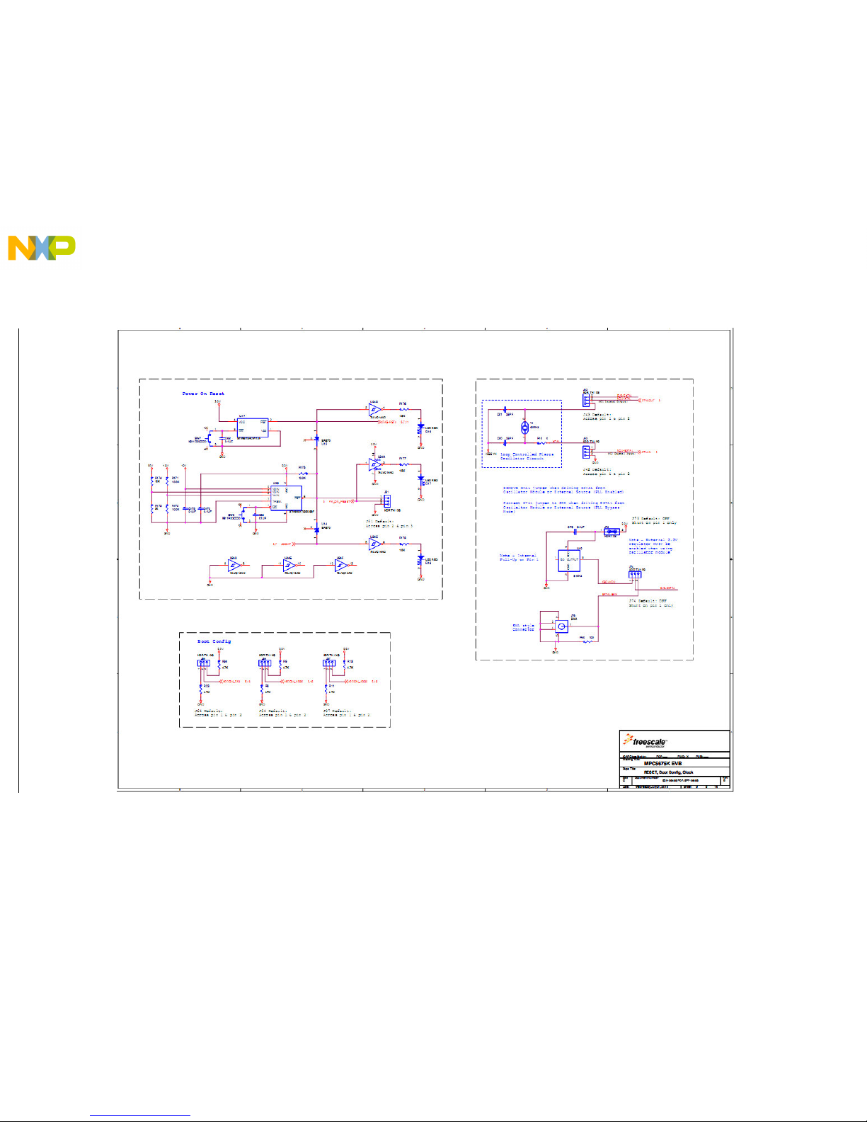
3.2.2 Reset Boot Configuration (J69, J34, J37)
The MPC5675 has 3 boot configuration jumpers (BOOTCFG) that determines the boot location of the
MCU based at POR (Power On Reset). This is shown in the table below:
Table 3-3 BOOTCFG Control
2-3 1-2 1-2 - Serial Boot LINFlex
2-3 1-2 2-3 - Serial Boot FlexCAN
2-3 2-3 1-2 - Serial Boot via LINFlexD or FlexCAN in autobaud
1-2 - - Valid SC (Single Chip)
1-2 - - Not Valid Safe Mode
3.3 ONCE and Nexus
The EVB supports a standard JTAG / ONCE cable with a 14-pin 0.1” walled header footprint. There is
also a 50-pin Samtec ERF8 connector for Nexus debug.
ON
3.3.1 Debug Connector Pinouts
The EVB is fitted with 14-pin JTAG / ONCE and 50-pin Nexus debug connectors. The following
diagram shows the 14-pin JTAG / ONCE connector pin out (0.1” keyed header).
TDI 1
TDO3
TCLK 5
5v EVTI 7
RESET 9
VDDE2 11
RDY 13
Figure 3-5. MPC5675 JTAG / ONCE Connector
The Nexus module used on the MPC5675K family uses the JTAG pins (for control of the Nexus block)
along with additional Nexus pins for trace messages. Nexus mode is entered by a JTAG sequence
whereby the Nexus EVTI pin is sampled on the rising edge of the JTAG TRST pin. If the EVTI is
asserted on TRST, Nexus is enabled.
The table below shows the pin out of the 50-pin Samtec ERF8 Nexus connector for the MPC5675K.
The new 50 pin Nexus connector has been used to support the new 16 MDO channels.
2 VSS
4 VSS
6 VSS
8 N/C
10 TMS
12 VSS
14 JCOMP
MPC5675EVB Page 5 of 29
Page 13

MPC5675EVB Users Manual Rev 2.0 July 2010
Pin
Function
BGA
Pin
Function
BGA
Table 3-4. NEXUS Debug Connector Pinout
No
No
1 MSEO[0] H3 2 V_DEBUG E1
3 MSEO[1] G4 4 TCK TCK
5 GND GND 6 TMS TMS
7 MDO0 E1 8 TDI TDI
9 MDO1 D1 10 TDO TDO
11 GND GND 12 JCOMP JCOMP
13 MDO2 E2 14 RDY J1
15 MDO3 D2 16 EVTI H4
17 GND GND 18 EVTO H1
19 MCKO G1 20 JTAG RST JTAG RST
21 MDO4 F4 22 RESET OUT RESET OUT
23 GND GND 24 GND GND
25 MDO5 A4 26 -
27 MDO6 F3 28 -
29 GND GND 30 GND GND
31 MDO7 A5 32 -
33 MDO8 G3 34 -
35 GND GND 36 GND
GND
37 MDO9 A6 38 -
39 MDO10 F1 40 -
41 GND GND 42 GND GND
43 MDO11 F2 44 MDO13 J2
45 MDO12 J3 46 MDO14 B5
47 GND GND 48 GND GND
49 MDO15 C2 50 -
Note - In order to preserve the ability to accurately measure power consumption on the MCU pins, the
JTAG and Nexus connector reference voltages will be sourced directly from the 5V regulator.
MPC5675EVB Page 6 of 29
Page 14
MPC5675EVB Users Manual Rev 2.0 July 2010
Jumper
Position
PCB Legend
Description
(D)
(D)
(D)
(D)
(D)
(D)
(D)
(D)
(D)
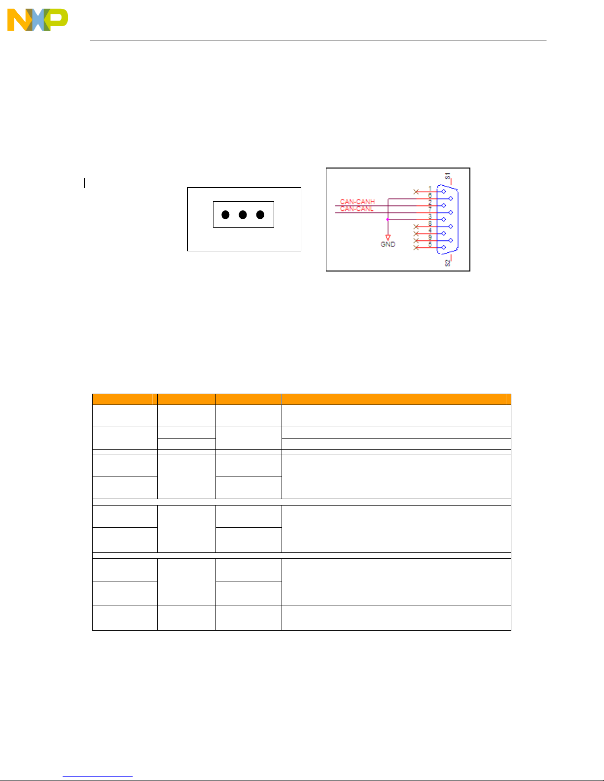
3.4 CAN Configuration (J21, J22, J29, J30, J31)
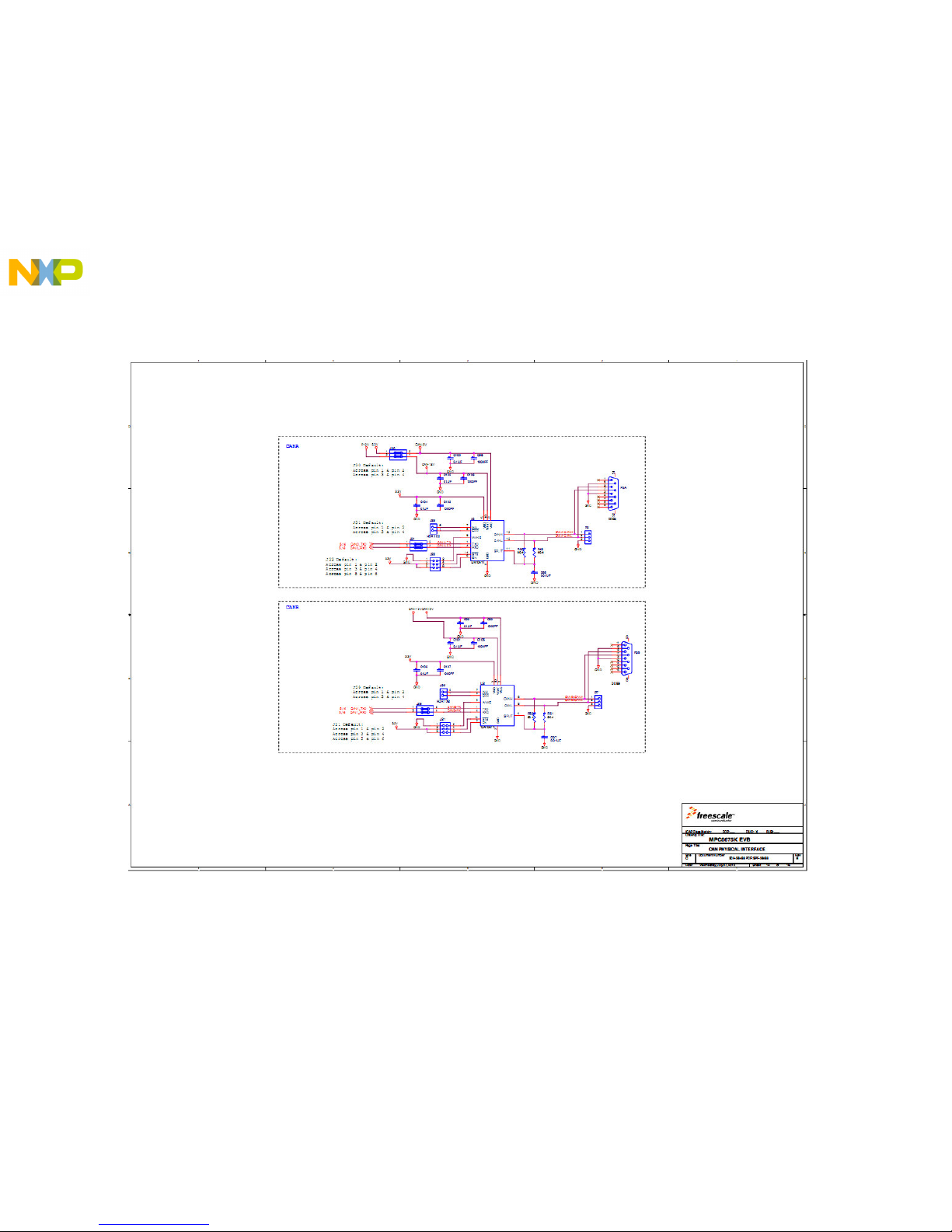
The EVB has 2x NXP TJA1041T high speed CAN transceiver on the MCU CAN-A and CAN-B
channels. These can operate with 5v or 3.3v I/O from the MCU. For flexibility, the CAN transceiver I/O
is connected to a standard 0.1” connector and DB9 connector at the top edge of the PCB. Connectors
P8 and P3A provides the CAN bus level signal interface for CAN-A and connector P7 and P3B for
CAN-B. The pin out for these connectors is shown below.
1
HI LOW
GND
Figure 3-6 CAN Physical Interface Connector
Each of the MCU signals to the CAN transceivers is jumpered, allowing the transceiver to be isolated
if that MCU pin is not configured or used for CAN operation. There is a 2x2 jumper for each CAN
channel (one for Rx, one for Tx). There are also two power jumpers (J30) to physically remove power
(12v and 5v) from both of the CAN transceivers. Jumpers J21 (CAN B) and J22 (CAN A) are
configuration jumpers for each of the Transceivers to control Wake, Standby and Enable. Jumpers
can be fitted to select default values or wires can be used to connect these pins to the MCU.
Table 3-5 CAN Control Jumpers (J30, J31, J21, J22)
J30
Posn 1-2
J30
Posn 3-4
J31 (CAN-A)
Posn 1-2
J31 (CAN-A)
Posn 3-4
J29 (CAN-B)
Posn 1-2
J29 (CAN-B)
Posn 3-4
J21 & J22
Posn 1-2
J21 & J22
Posn 3-4
J21 & J22
Posn 5-6
FITTED
REMOVED
FITTED
REMOVED
FITTED
REMOVED
FITTED
REMOVED
FITTED
REMOVED
FITTED
REMOVED
FITTED
REMOVED
FITTED
REMOVED
FITTED
REMOVED
TX
RX
TX
RX
WAKE
STB
EN
5v is applied to both CAN transceivers VCC
No 5v power is applied to CAN transceivers
12v Power is applied to both CAN transceivers VBAT
No 12v power is applied to CAN transceivers
MCU CAN0_TXD is connected to CAN controller A
MCU CAN0_TXD is NOT routed to CAN controller.
MCU CAN0_RXD is connected to CAN controller A
MCU CAN0_RXD is NOT routed to CAN controller.
MCU CAN1_TXD is connected to CAN controller B
MCU CAN1_TXD is NOT routed to CAN controller.
MCU CAN1_RXD is connected to CAN controller B
MCU CAN1_RXD is NOT routed to CAN controller.
CAN Transceiver WAKE is connected to GND
WAKE is not connected and available on Pin 2
CAN Transceiver STB is connected to 5v
STB is not connected and available on Pin 4
CAN Transceiver is Enabled
EN is not connected and available on Pin 6
Access to the Error and inhibit signals from the transceivers is provided on J32 and J33.
Notes
- Care should be taken when fitting the jumper headers as they can easily be fitted in the
incorrect orientation.
MPC5675EVB Page 7 of 29
Page 15
MPC5675EVB Users Manual Rev 2.0 July 2010
Jumper
Position
Description
(D)
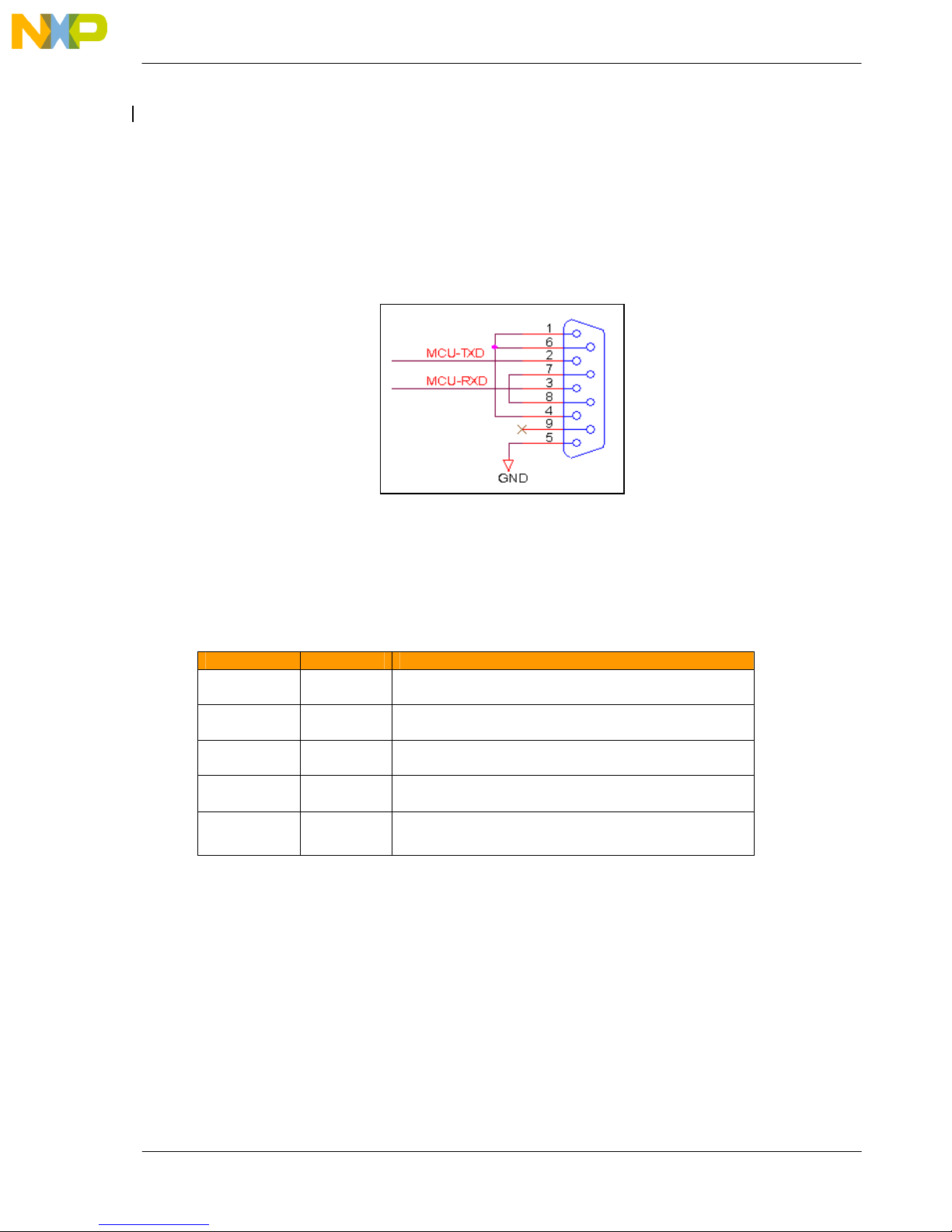
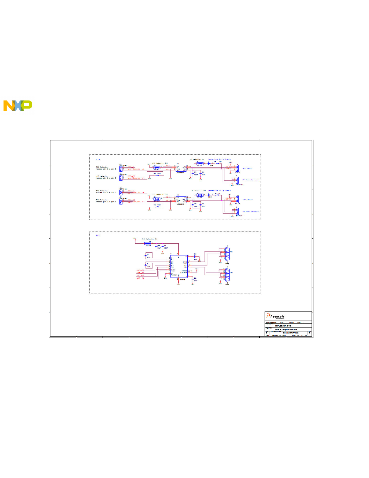
3.5 RS232 Configuration (J5,J6,J15, J16, J23)
The EVB has a single MAX3223 RS232 transceiver device, providing RS232 signal translation for the
MCU SCI channels A and B.
Each of the two RS232 outputs from the MAX3223 device is connected to a DB9 connector, allowing
a direct RS232 connection to a PC or terminal. Connector P2A provides the RS232 level interface for
MCU SCI-A and P2B for MCU SCI-B. The pinout of these connectors is detailed below. Note that
hardware flow control is not supported on this implementation.
Figure 3-7 RS232 Physical Interface Connector
The MPC5675 SCI also provides hardware LIN master capability which is supported on the EVB via
LIN transceivers. Jumpers J17, J18, J23 and J24 are provided to isolate the MCU SCI signals from
the RS232 interface as described below. There is also a global power jumper (J15) controlling the
power to the RS232 transceiver.
Table 3-6 RS232 Control Jumpers
J15
(SCI-PWR)
J18 (SCI-A)
J17 (SCI-A)
J19 (SCI-B)
FITTED
REMOVED
2-3 MCU TXD-A is routed to MAX3223
REMOVED MCU TXD-A signal is disconnected from CAN/LIN
2-3 MCU RXD-A is routed via MAX3223
REMOVED MCU RXD-A signal is disconnected from CAN/LIN
2-3 MCU TXD-B is routed via MAX3223
REMOVED MCU TXD-B signal is disconnected from CAN/LIN
Power is applied to the MAX3223 transceiver
No power is applied to the MAX3223 transceiver
2-3 MCU RXD-B is routed via MAX3223
J20 (SCI-B)
REMOVED MCU RXD-B signal is disconnected from CAN/LIN
The default configuration enables SCI-A and SCI-B channels. RS232 compliant interfaces (with no
hardware flow control) are available at DB9 connector P1. If the MCU is configured such that SCI-A or
SCI-B is set as a normal I/O port, then the relevant jumpers must be removed to avoid any conflicts
occurring. If required, jumper J15 can be used to completely disable the SCI transceiver.
MPC5675EVB Page 8 of 29
Page 16
MPC5675EVB Users Manual Rev 2.0 July 2010
Jumper
Position
Description
(D)
(D)
(D)
(D)
LIN
LIN Configuration (J5, J6, J16, J23,J18,J17,J19,J20)
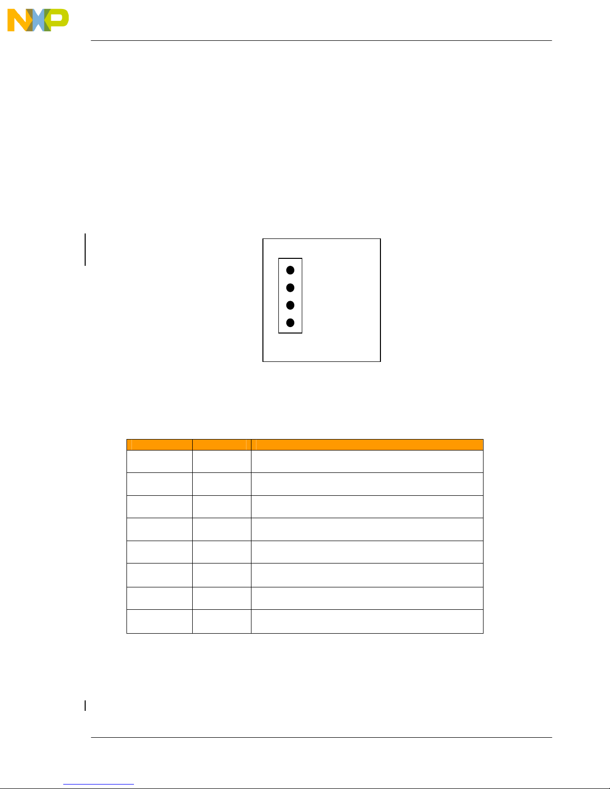
The EVB is fitted with two Freescale MCZ33661EF LIN transceivers. The LINFLEX module
incorporates a UART mode, and as such, the LIN transceivers are connected to the TX and RX
signals of SCI via UART A and B.
For flexibility, the LIN transceivers are connected to a standard 0.1” connector (P9 for LIN-C and P10
for LIN-D) and a 4 pin molex connector (J1 for LIN-A and J2 for LIN-B) at the top edge of the PCB as
shown in the figure below.
For ease of use, the 12V EVB supply is fed to pin1 of the P9, P10 headers and the LIN transceiver
power input to pin 2. This allows the LIN transceiver to be powered directly from the EVB supply by
simply linking pins 1 and 2 of header P9/P10 using a 0.1” jumper shunt.
Figure 3-8 LIN Physical Interface Connectors
Along with the MCU signal routing jumpers (J17 / J18 /J19 / J20), there is are jumpers (J16 / J23) to
enable or disable the LIN transceiver and jumpers (J5 and J6) which determines if the LIN transceiver
is operating in master or slave mode, as defined in the table below.
Table 3-7 LIN Control Jumpers
P9/P10
1
VDD UNREG
LIN VSUP
LIN
GND
J5
J6
J16
J23
J18
J17
J19
J20
FITTED
REMOVED
FITTED
REMOVED
FITTED
REMOVED The LIN-A transceiver is disabled
FITTED
REMOVED The LIN-B transceiver is disabled
2-3 MCU LIN0_TXD is connected to SCI_A TX
1-2 MCU LIN0_TXD is connected to LIN Physical
2-3 MCU LIN0_RXD is connected to SCI_A TX
1-2 MCU LIN0_RXD is connected to LIN Physical
2-3 MCU LIN1_TXD is connected to SCI_B TX
1-2 MCU LIN1_TXD is connected to LIN Physical
2-3 MCU LIN1_RXD is connected to SCI_B TX
1-2 MCU LIN1_RXD is connected to LIN Physical
LIN-A transceiver is configured for LIN Master mode
LIN-A transceiver is configured for LIN Slave mode
LIN-B transceiver is configured for LIN Master mode
LIN-B transceiver is configured for LIN Slave mode
The LIN-A transceiver is enabled
The LIN-B transceiver is enabled
* Note – Jumpers J16/J23 do NOT route power to LIN transceivers, they only control an enable line
on the LIN device. Power to the LIN transceiver is supplied via connectors P9/ P10, Pin 2.
The Default LIN configuration is with the module enabled in master mode, LIN slave mode can be
enabled by removing jumpers J5 / J6.
MPC5675EVB Page 9 of 29
Page 17

MPC5675EVB Users Manual Rev 2.0 July 2010
Jumper
Position
PCB
Description
(D)
(D)
(D)
(D)
(D)
(D)
Jumper
Position
PCB
Description
(D)
REMOVED
12V Flexray circuitry is not powered
(D)
(D)
3.6 FlexRAY Configuration
(J19, J27, J25, J26, J28)
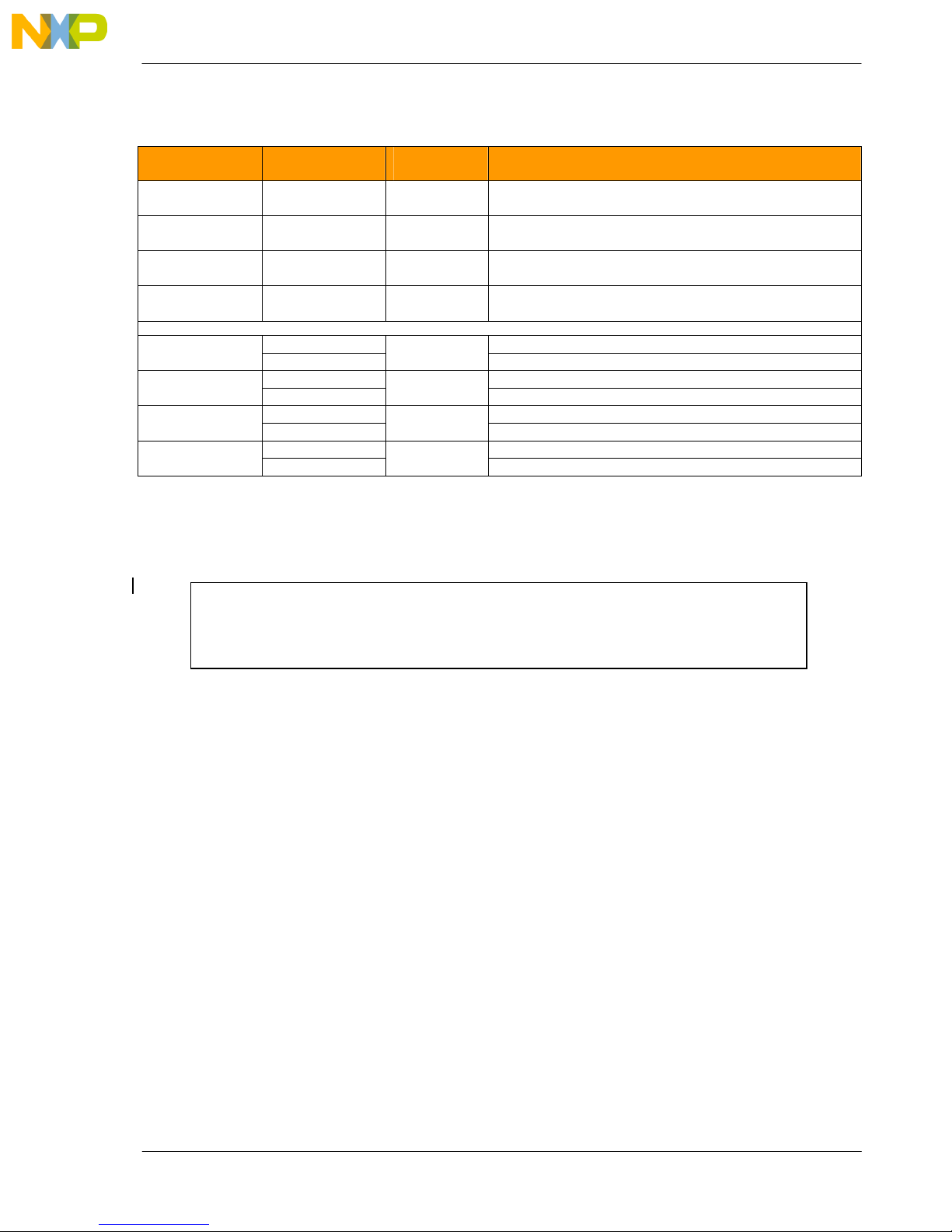
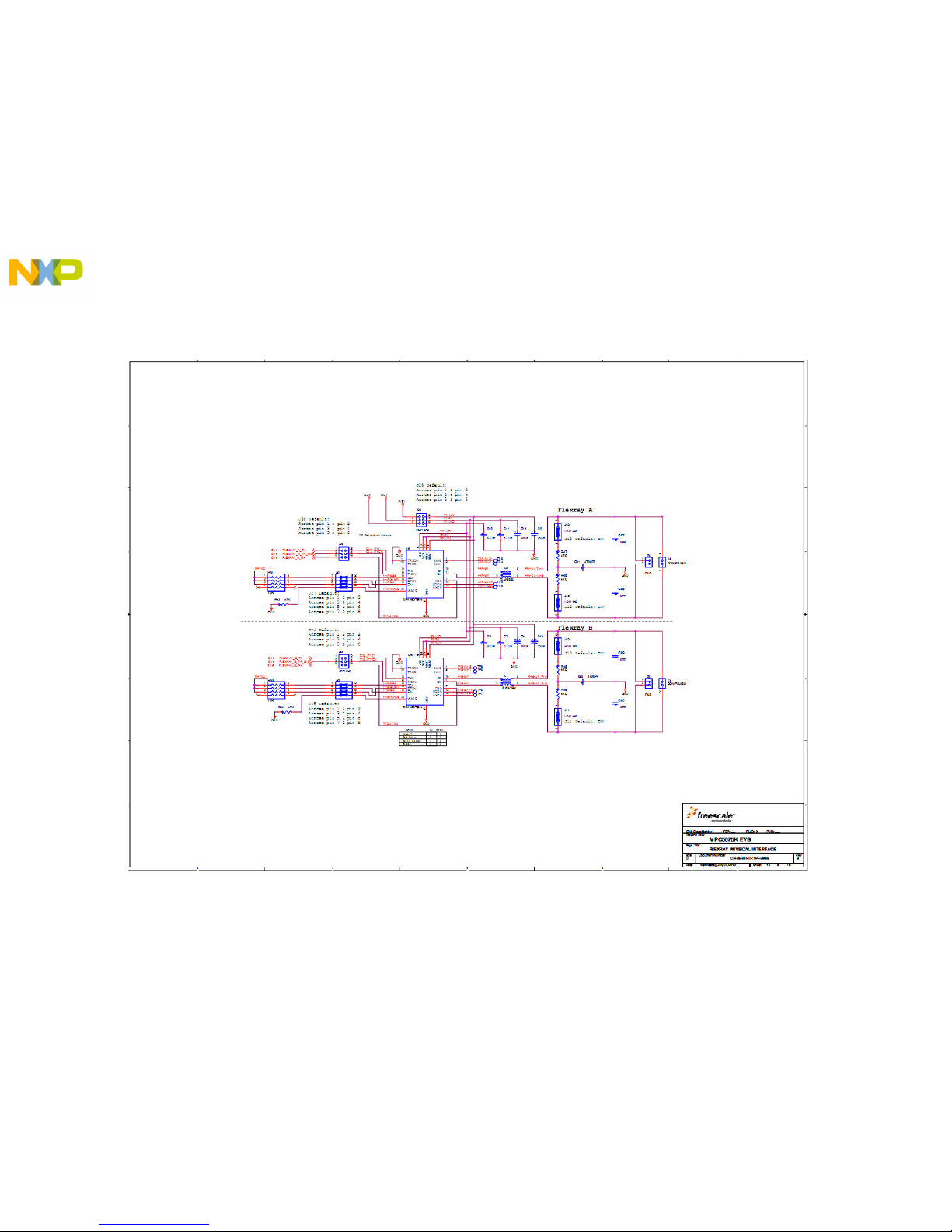
The EVB is fitted with 2 FlexRAY physical interfaces connected to MCU FlexRAY channels A and B.
Jumpers J19 and J27 are provided to route the respective MCU signals to the physical interfaces as
described below.
Table 3-8 Flexray MCU Signal Routing Jumpers (J19, J27)
Legend
J26 (Flex-A)
Posn 1-2
J26 (Flex-A)
Posn 3-4
J26 (Flex-A)
Posn 5-6
J24 (Flex-B)
Posn 1-2
J24 (Flex-B)
Posn 3-4
J24(Flex-B)
Posn 5-6
FITTED
REMOVED MCU B8 is not connected to Flexray A transceiver TX
FITTED
REMOVED MCU A8 is not connected to Flexray A transceiver TXEN
FITTED
REMOVED MCU E3 is not connected to Flexray A transceiver RXEN
FITTED
REMOVED MCU A7 is not connected to Flexray B transceiver TX
FITTED
REMOVED MCU B7 is not connected to Flexray B transceiver TXEN
FITTED
REMOVED MCU C5 is not connected to Flexray B transceiver RXEN
TX
TXEN
RX
TX
TXEN
RX
The power to the Flexray physical interface is controlled via jumper J28 to allow disconnection if
required.
Table 3-9 Flexray Power Control Jumpers (J25)
MCU B8 is connected to Flexray A transceiver TX
MCU A8 is connected to Flexray A transceiver TXEN
MCU E3 is connected to Flexray A transceiver RX
MCU A7 is connected to Flexray B transceiver TX
MCU B7 is connected to Flexray B transceiver TXEN
MCU C5 is connected to Flexray B transceiver RX
Legend
J28 (Flex-PWR)
Posn 1-2
J28 (Flex-PWR)
Posn 3-4
J28 (Flex-PWR)
Posn 5-6
FITTED
FITTED
REMOVED 5V Flexray circuitry is not powered
FITTED
REMOVED VIO Flexray circuitry is not powered
12V
5V
VIO
12V Flexray circuitry is powered from main 12V input
5V Flexray circuitry is powered from 5.0V switching reg
VIO Flexray circuitry is powered from 3.3v
The flexray interface has 4 pins which are used for configuration and are pulled high or low controlled
by a jumper as described in the table below. By default, all of the jumper headers are fitted. Please
consult the Flexray physical interface specification before changing any of these jumpers.
MPC5675EVB Page 10 of 29
Page 18
MPC5675EVB Users Manual Rev 2.0 July 2010
Jumper
Position
PCB
Description
(D)
(D)
(D)
(D)
J25 (Flex
-B)
(D)
J25 (Flex
-B)
(D)
J25 (Flex
-B)
(D)
J25 (Flex
-B)
(D)
Important:
Table 3-10 Flexray Control Jumpers (J26, J28)
Legend
J27 (Flex-A)
Posn 1-2
J27 (Flex-A)
Posn 3-4
J27 (Flex-A)
Posn 5-6
J27 (Flex-A)
Posn 7-8
FITTED
REMOVED Flexray-A interface BGE signal is unterminated
FITTED
REMOVED Flexray-A interface EN signal is unterminated
FITTED
REMOVED Flexray-A interface STBN signal is unterminated
FITTED
REMOVED Flexray-A interface WAKE signal is unterminated
BGE
EN
STBEN
WAKE
Flexray-A interface BGE signal is pulled to VIO
Flexray-A interface EN signal is pulled to VIO
Flexray-A interface STBN signal is pulled to VIO
Flexray-A interface WAKE signal is pulled to GND
Posn 1-2
Posn 3-4
Posn 5-6
Posn 7-8
FITTED
REMOVED Flexray-B interface BGE signal is unterminated
FITTED
REMOVED Flexray-B interface EN signal is unterminated
FITTED
REMOVED Flexray-B interface STBN signal is unterminated
FITTED
REMOVED Flexray-B interface WAKE signal is unterminated
BGE
EN
STBEN
WAKE
Flexray-B interface BGE signal is pulled to VIO
Flexray-B interface EN signal is pulled to VIO
Flexray-B interface STBN signal is pulled to VIO
Flexray-B interface WAKE signal is pulled to GND
Notes:
- The flexray physical interfaces are connected to 2 pin molex connectors (FlexRAY A) 1.25mm
shrouded 2-pin connectors to connect to the flexray bus (as are standard fit on many
Freescale development platforms using flexray).
A 40Mhz oscillator is required for the correct operation of the flexray controller. Please
ensure that the 40Mhz crystal is selected as the system clock or use a 40Mhz external
clock source.
MPC5675EVB Page 11 of 29
Page 19
MPC5675EVB Users Manual Rev 2.0 July 2010
Port Pin
Pull Direction
Strength
FEC_CRS
FEC_RX_ER
FEC_RX_DV
FEC_RXD0
FEC_RXD1
FEC_RXD2
FEC_RXD3
FEC_TX_EN
FEC_TXD0
FEC_TXD1
FEC_TXD2
FEC_TXD3
Jumper
Position
PCB
Description
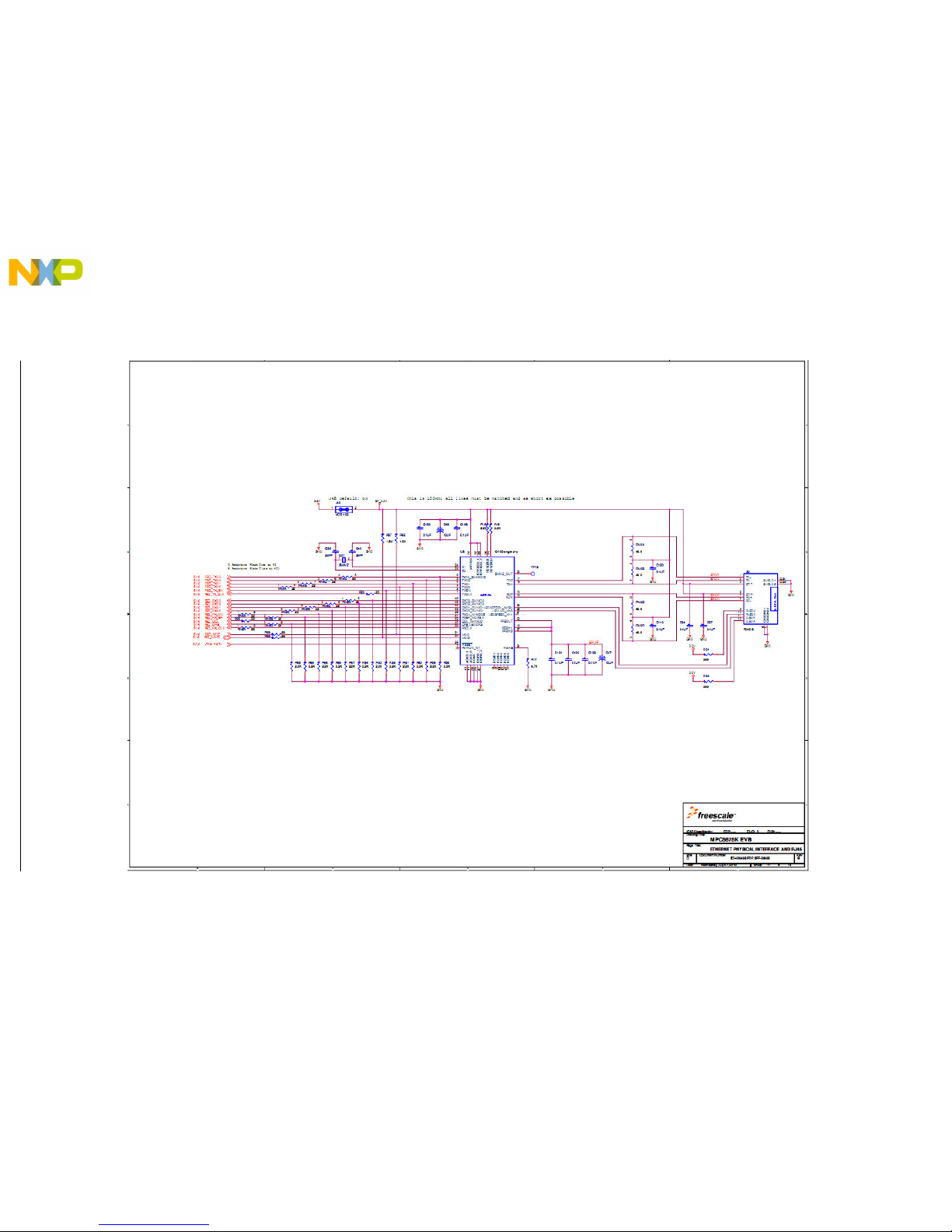
3.7 Ethernet
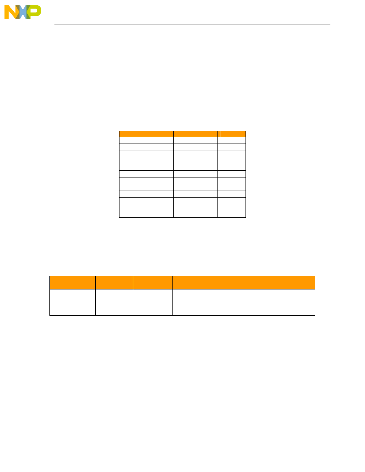
The EVB is fitted with a National Semiconductor DP8348C Ethernet physical interface (U8) and a
RJ45 connector with integrated activity LED’s and magnetics (J51).
The National Semiconductor DP8348C physical interface is connected to the MII on the MPC5675.
This is a fixed connection with no means of isolation. Pullups are also also present on some of these
signals. These are detailed in the table below. Please be aware of this when using the related GPIOs.
Table 3-11 Pull up/ Pull down resistors for Ethernet Physical
The voltage domain that is used by the GPIO should be set to 3.3v when power is applied to the
physical interface.
Power can be removed from the physical interface via J48.
Table 3-12 Ehternet Physical Interface Power Supply Enabled (J48)
Down (GND) 2.2kΩ
Down (GND) 2.2kΩ
Down (GND) 2.2kΩ
Down (GND) 2.2kΩ
Down (GND) 2.2kΩ
Down (GND) 2.2kΩ
Down (GND) 2.2kΩ
Down (GND) 2.2kΩ
Down (GND) 2.2kΩ
Down (GND) 2.2kΩ
Down (GND) 2.2kΩ
Down (GND) 2.2kΩ
Legend
J48
(PHY PWR)
FITTED (D)
PHY PWR
REMOVED
The DP4348C Ethernet Physical Interface is powered
from the 3.3v SR.
The DP4348C Ethernet Physical Interface is not
powered
MPC5675EVB Page 12 of 29
Page 20
MPC5675EVB Users Manual Rev 2.0 July 2010
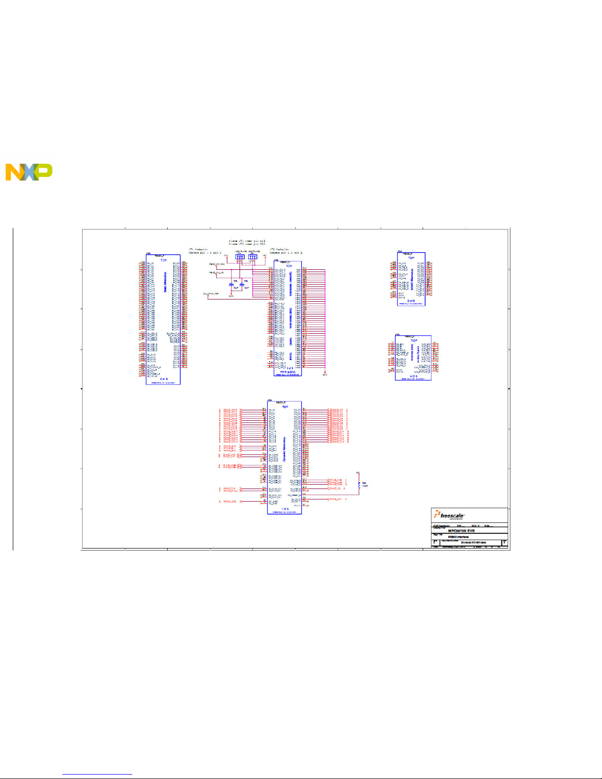
3.8 PISMO DRAMC Connector
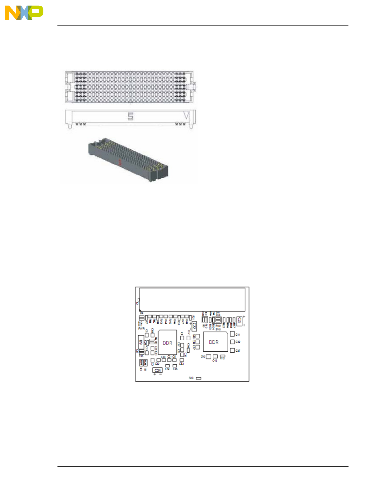
The PISMO02-00040 board connector provided by Samtec is available for connecting DDR1, DDR2
or mDDR (LPDDR) to the EVB. Appropriate RAM daughter cards are available from Micron. Such as
PISMO2 00002 (MT47H128M16HG-25:A)
MPC5675EVB Page 13 of 29
Page 21

MPC5675EVB Users Manual Rev 2.0 July 2010
J37 Short 1
-2 1
MCRGM_ABS2 is tied to ground
4. Default Jumper Summary Table
473BGA ONLY
The following table details the DEFAULT jumper configuration of the EVB as explained in detail in
section 3. 473BGA ONLY
Table 4-1 Default Jumper Positions
Jumper Reference
Default Setting Jump Count Description
J77 ON 1 NOW BEEN REMOVED from Rev_B
J41 ON 1 Power on VDD_HV_IO is enabled
J63 Short 2-3 1 Power on VDD_HV_DRAM is 3.3V
J58 ON 1 VDD_HV_DRAM_VTT is grounded.
J55 ON 1 Power on VDD_HV_FLA is enabled
J56 ON 1 Power on VDD_HV_PDI is enabled
J40 ON 1 Power on VDD_HV_OSC is enabled
J44 ON 1 Power on VDD_HV_ADV is enabled
J78 Short 1-2 1 Power on VDD_HV_ADR is 5.0V
J46 OFF 0 Power on VDD_LV_COR is disabled
J59 ON 1 Internal power is enabled
J57 ON 1 Internal power is enabled
J79 Short 2-3 1 Internal power is enabled and 3.3V to VDD_PMU
J62 Short 2-3 1 Internal power is enabled
J83 Short1-2 1 VPP_TEST is tied to GND
J38
OFF (place on
PIN1 only)
1 POTS on ADC0 is disabled
J61 Short 2-3 1 PW_ON_RESET is tied to ground
J64 Short 1-2 1 MCRGM_FAB is tied to ground
J34 Short 1-2 1 MCRGM_ABS0 is tied to ground
J43 Short 1-2 1 Use on board 40.0MHz crystal
J42 Short 1-2 1 Use on board 40.0MHz crystal
J73
J74
OFF (place on
PIN1 only)
OFF (place on
PIN1 only)
1
1
Use on board 40.0MHz crystal
Use on board 40.0MHz crystal
J71 Short 1-2 1 Power on PISMO_DM_VCC is 3.3V
J72 Short 1-2 1 Power on PISMO_DM_VIO is 3.3V
J48 ON 1 Power on Ethernet PHY is enabled
J30 ON 2 Power on CAN PHY is enabled
J31 ON 2 CANA TXD & RXD are connected to MCU
J22 ON 3 CANA control signals are on
J29 ON 2 CANB TXD & RXD are connected to MCU
J21 ON 3 CANB control signals are on
J18 Short 2-3 1 UART TXD is connected to MCU
J17 Short 2-3 1 UART RXD is connected to MCU
J19 Short 2-3 1 UART TXD is connected to MCU
J20 Short 2-3 1 UART RXD is connected to MCU
J16 ON 1 Power on LINC is enabled
J5 ON 1 LINC Bus Master Mode is enabled
J23 ON 1 Power on LIND is enabled
J6 ON 1 LIND Bus Master Mode is enabled
J15 ON 1 Power on SCI is enabled
J28 ON 3 Power on Flexray is enabled
MPC5675EVB Page 14 of 29
Page 22

MPC5675EVB Users Manual Rev 2.0 July 2010
J26 ON 3 FlexrayA data signals are connected to MCU
J27 ON 4 FlexrayA control signals are on
J24 ON 3 FlexrayB data signals are connected to MCU
J25 ON 4 FlexrayB control signals are on
J13 ON 1 FlexrayA decoupling capacitor is disabled
J12 ON 1 FlexrayA decoupling capacitor is disabled
J10 ON 1 FlexrayB decoupling capacitor is disabled
J11 ON 1 FlexrayB decoupling capacitor is disabled
J39 ON 1 FLEXPWM0_B1 is enabled to LED
J49 ON 1 FLEXPWM0_B0 is enabled to LED
J50 ON 1 FLEXPWM0_A3 is enabled to LED
J52 ON 1 FLEXPWM0_A2 is enabled to LED
J54 ON 1 FLEXPWM0_X2 is enabled to LED
J80 ON 1 FLEXPWM0_X3 is enabled to LED
J81 ON 1 FLEXPWM0_A1 is enabled to LED
J82 ON 1 FLEXPWM0_B3 is enabled to LED
MPC5675EVB Page 15 of 29
Page 23
MPC5675EVB Users Manual Rev 2.0 July 2010
Function
Function
Function
Function
15
16
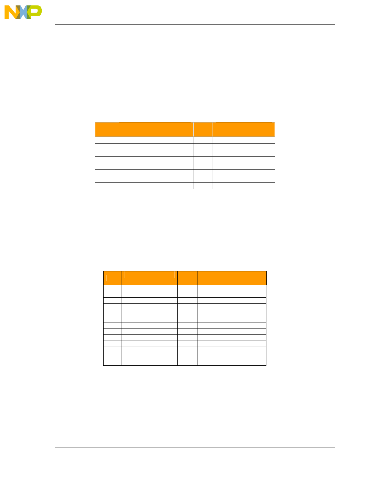
5. User Connector Descriptions
This section details the pinout of the EVB user connectors. The connectors are 0.1 inch pitch turned
pin headers and are located at various locations on the EVB. They are grouped by port functionality
and the PCB legend shows the respective port number adjacent to each pin.
5.1.1 eTimer (Connector J65)
Table 5-1 eTimer Connector Pinout (J65)
Pin
1 ETIMER0_ETC0 2 ETIMER1_ETC0
3 ETIMER0_ETC1 4 ETIMER1_ETC1
5 ETIMER0_ETC2 6 ETIMER1_ETC2
7 ETIMER0_ETC3 8 ETIMER1_ETC3
9 ETIMER0_ETC4 10 ETIMER1_ETC4
11 ETIMER0_ETC5 12 ETIMER1_ETC5
13 GND 14 GND
5.1.2 ADC 0/1 (Connector J60)
Table 5-2 ADC 0/1 Connector Pinout (J60)
Pin
1 GND 2 GND
3 ADC0_AN0 4 ADC1_AN0
5 ADC0_AN1 6 ADC1_AN1
7 ADC0_AN2 8 ADC1_AN2
9 ADC0_AN3 10 ADC1_AN3
11 ADC0_AN4 12 ADC1_AN4
13 ADC0_AN5 14 ADC1_AN5
ADC0_AN6
17 ADC0_AN7 18 ADC1_AN7
19 ADC0_AN8 20 ADC1_AN8
21 ADC0_ADC1_AN11 22 ADC0_ADC1_AN13
23 ADC0_ADC1_AN12 24 ADC0_ADC1_AN14
25 GND 26 GND
Pin
Pin
ADC1_AN6
MPC5675EVB Page 16 of 29
Page 24
MPC5675EVB Users Manual Rev 2.0 July 2010
Function
Function
Function
Function
Function
Function
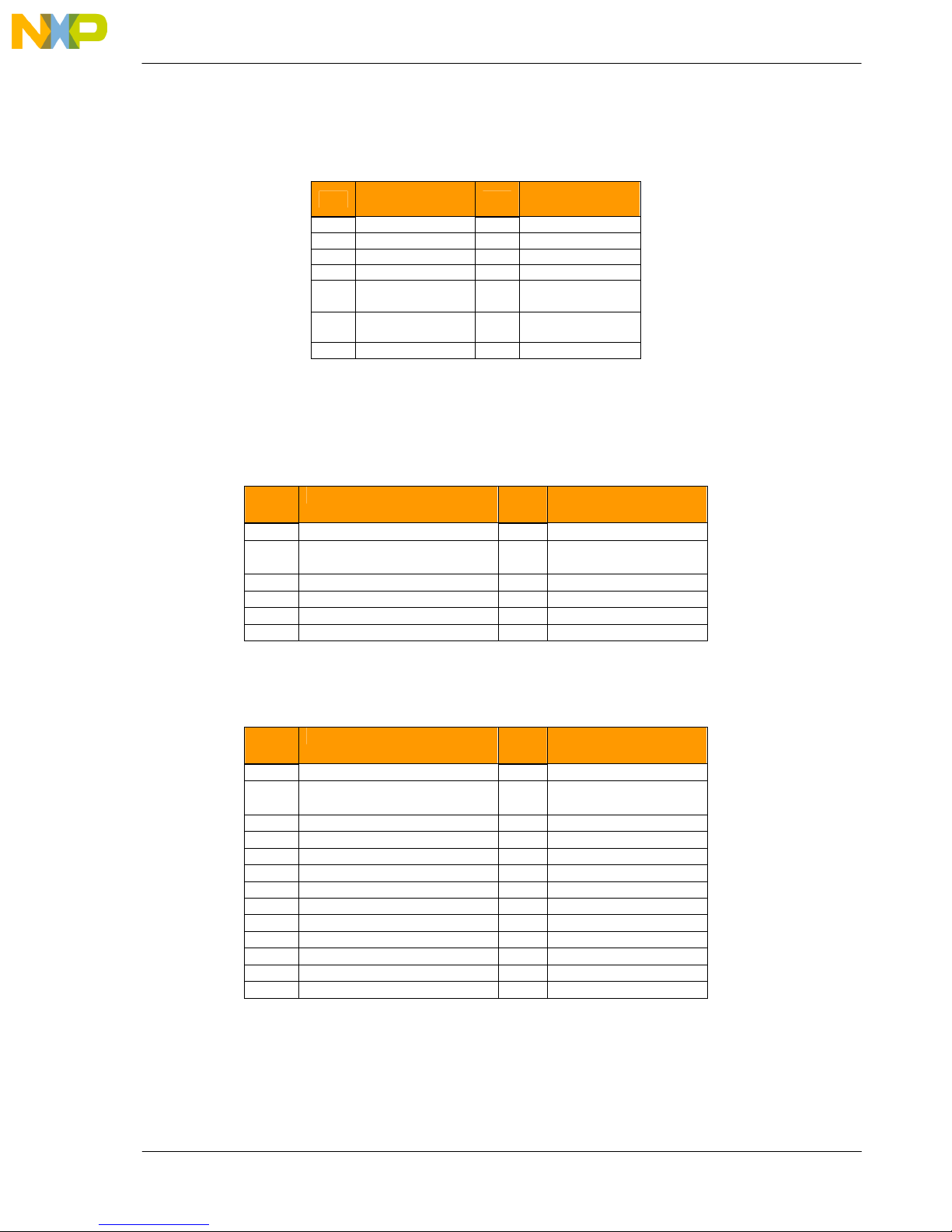
5.1.3 ADC 2/3 (Connector J47)
Table 5-3 ADC 2/3 Connector Pinout (J47)
Pin
1 ADC2_AN0 2 ADC3_AN0
3 ADC2_AN1 4 ADC3_AN1
5 ADC2_AN2 6 ADC3_AN2
7 ADC2_AN3 8 ADC3_AN3
ADC2_ADC3_AN
9
11
13 GND 14 GND
11
ADC2_ADC3_AN
12
5.1.4 EBI (Connector J66, J69, J70)
Table 5-4 EBI Connector Pinout (J66)
Pin
1 GND 2 GND
3 EBI_CS0 4 EBI_WE_BE_0
5 EBI_CS1 6 EBI_WE_BE_1
7 EBI_OE 8 EBI_WE_BE_2
9 EBI_TS 10 EBI_WE_BE_3
11 EBI_BDIP 12 EBI_CLKOUT
Pin
ADC2_ADC3_AN
10
ADC2_ADC3_AN
12
Pin
13
14
Table 5-5 EBI Connector Pinout (J69)
Pin
1 GND 2 GND
3 EBI_ADD12 / EBI_ALE 4 EBI_ADD11 / EBI_TEA
5 EBI_ADD13 6 EBI_ADD10 / EBI_TA
7 EBI_ADD14 8 EBI_ADD9 / EBI_CS3
9 EBI_ADD15 10 EBI_ADD8 / EBI_CS2
11 GND 12 GND
13 GND 14 GND
15 EBI_D0 / EBI_ADD16 16 EBI_D16
17 EBI_D1 / EBI_ADD17 18 EBI_D17
19 EBI_D2 / EBI_ADD18 20 EBI_D18
21 EBI_D3 / EBI_ADD19 22 EBI_D19
23 EBI_D4 / EBI_ADD20 24 EBI_D20
25 EBI_D5 / EBI_ADD21 26 EBI_D21
Pin
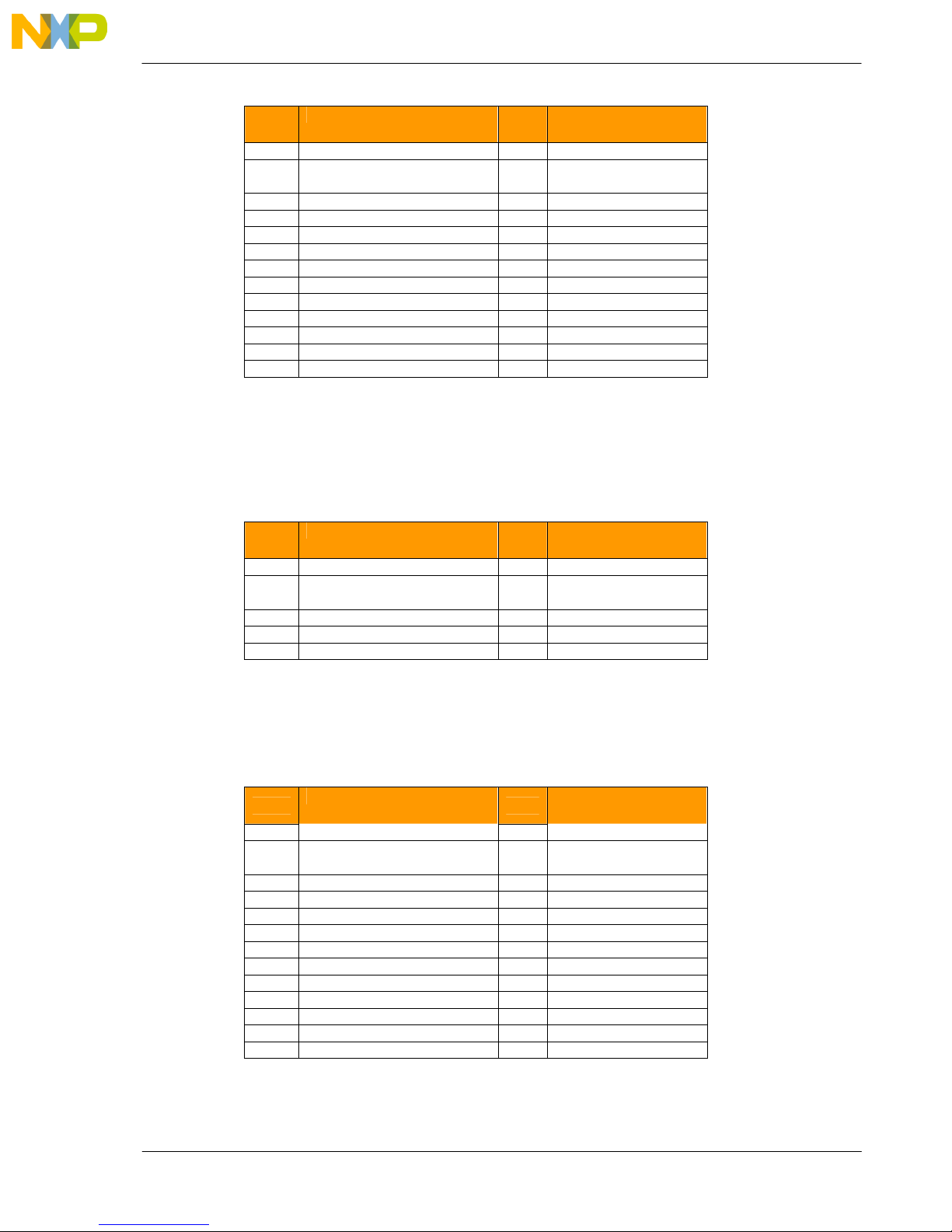
Table 5-6 EBI Connector Pinout (J70)
MPC5675EVB Page 17 of 29
Page 25
MPC5675EVB Users Manual Rev 2.0 July 2010
Function
Function
Function
Function
Function
Function
Pin
1 EBI_D6 / EBI_ADD22 2 EBI_D22
3 EBI_D7 / EBI_ADD23 4 EBI_D23
5 GND 6 GND
7 EBI_D8 / EBI_ADD24 8 EBI_D24
9 EBI_D9 / EBI_ADD25 10 EBI_D25
11 EBI_D10 / EBI_ADD26 12 EBI_D26
13 EBI_D11 / EBI_ADD27 14 EBI_D27
15 EBI_D12 / EBI_ADD28 16 EBI_D28
17 EBI_D13 / EBI_ADD29 18 EBI_D29
19 EBI_D14 / EBI_ADD30 20 EBI_D30
21 EBI_D15 / EBI_ADD31 22 EBI_D31
23 GND 24 GND
25 GND 26 GND
5.1.5 NMI / FCC / CG (J45)
Table 5-7 NMI / FCC / CG Connector Pinout (J45)
Pin
1 NMI 2 GND
3 GND 4 MC_CGL_CLK_OUT1
5 FCCU0_F1 6 GND
7 GND 8 MC_CGL_CLK_OUT2
9 FCCU0_F0 10 GND
Pin
Pin
5.1.6 PDI (J67)
Table 5-8 PDI Connector Pinout (J67)
Pin
1 GND 2 GND
3 PDI_DATA0 4 PDI_DATA8
5 PDI_DATA1 6 PDI_DATA9
7 PDI_DATA2 8 PDI_DATA10
9 PDI_DATA3 10 PDI_DATA11
11 PDI_DATA4 12 PDI_DATA12
13 PDI_DATA5 14 PDI_DATA13
15 PDI_DATA6 16 PDI_DATA14
17 PDI_DATA7 18 PDI_DATA15
19 GND 20 GND
21 GND 22 PDI_FRAME_V
23 PDI_CLOCK 24 PDI_LINE_V
25 GND 26 GND
MPC5675EVB Page 18 of 29
Pin
Page 26
MPC5675EVB Users Manual Rev 2.0 July 2010
Function
Function
Function
Function
Function
Function
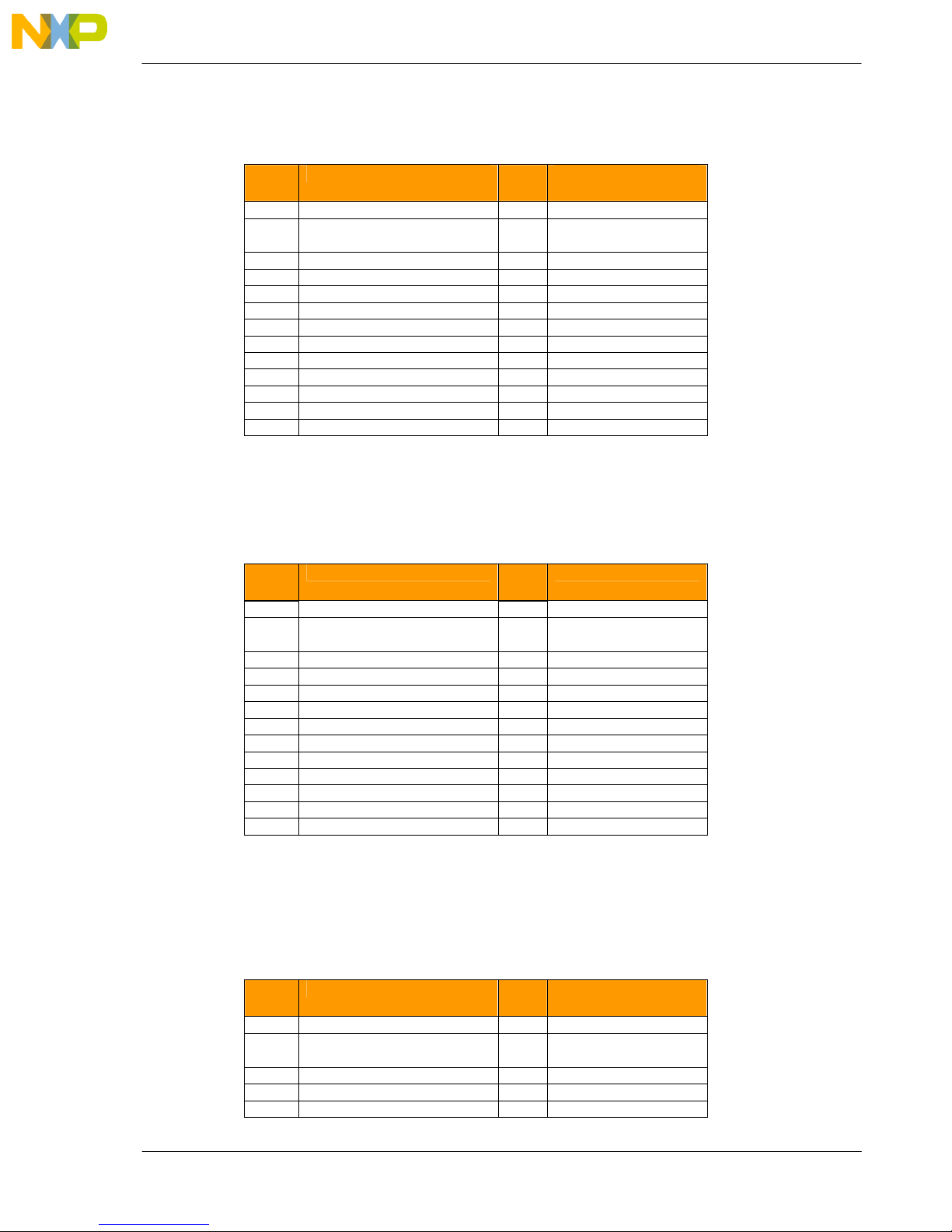
5.1.7 FLEXPWM (J8)
Table 5-9 FLEXPWM Connector Pinout (J8)
Pin
11 FLEXPWM0_B1 12 FLEXPWM1_B1
13 FLEXPWM0_B2 14 FLEXPWM1_B2
15 FLEXPWM0_B3 16 FLEXPWM1_B3
17 FLEXPWM0_X0 18 FLEXPWM1_X0
19 FLEXPWM0_X1 20 FLEXPWM1_X1
21 FLEXPWM0_X2 22 FLEXPWM1_X2
23 FLEXPWM0_X3 24 FLEXPWM1_X3
25 GND 26 GND
5.1.8 FEC (J68)
Pin
11 FEC_TXD3 12 FEC_RXD3
13 GND 14 GND
15 FEC_TX_EN 16 FEC_RX_DV
17 FEC_TX_ER 18 FEC_RX_ER
19 GND 20 GND
21 FEC_CRS 22 FEC_MDC
23 FEC_COL 24 FEC_MDIO
25 26 GND
Pin
1 FLEXPWM0_A0 2 FLEXPWM1_A0
3 FLEXPWM0_A1 4 FLEXPWM1_A1
5 FLEXPWM0_A2 6 FLEXPWM1_A2
7 FLEXPWM0_A3 8 FLEXPWM1_A3
9 FLEXPWM0_B0 10 FLEXPWM1_B0
Table 5-10 FEC Connector Pinout (J68)
Pin
1 GND 2 GND
3 FEC_TX_CLK 4 FEC_RX_CLK
5 FEC_TXD0 6 FEC_RXD0
7 FEC_TXD1 8 FEC_RXD1
9 FEC_TXD2 10 FEC_RXD2
5.1.9 FLEXRAY (J36)
Pin
1 GND 2 GND
3 FLEXRAY_A_TR_EN 4 FLEXRAY_B_TR_EN
5 FLEXRAY_A_TX 6 FLEXRAY_B_TX
7 FLEXRAY_A_RX 8 FLEXRAY_B_RX
9 GND 10 GND
MPC5675EVB Page 19 of 29
Table 5-11 FLEXRAY Connector Pinout (J36)
Pin
Page 27
MPC5675EVB Users Manual Rev 2.0 July 2010
Function
Function
Function
Function
5.1.10 LINFLEX / FLEXCAN (J35)
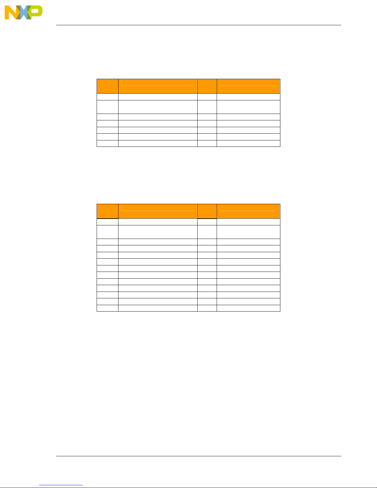
Table 5-12 LIN / CAN Connector Pinout (J35)
Pin
11 CAN0_RXD 12 CAN1_RXD
13 GND 14 GND
5.1.11 DSPI (J7)
Pin
11 DSPI1_CS0 12 DSPI1_SCK
13 DSPI1_CS2 14 DSPI1_SIN
15 DSPI1_CS3 16 DSPI1_SOUT
17 GND 18 GND
19 DSPI2_CS0 20 DSPI2_SCK
21 DSPI2_CS1 22 DSPI2_SIN
23 DSPI2_CS2 24 DSPI2_SOUT
25 GND 26 GND
Pin
1 GND 2 GND
3 LIN0_TXD 4 LIN1_TXD
5 LIN0_RXD 6 LIN1_RXD
7 GND 8 GND
9 CAN0_TXD 10 CAN1_TXD
Table 5-13 DSPI Connector Pinout (J7)
Pin
1 GND 2 GND
3 DSPI0_CS0 4 DSPI0_SCK
5 DSPI0_CS2 6 DSPI0_SIN
7 DSPI0_CS3 8 DSPI0_SOUT
9 GND 10 GND
MPC5675EVB Page 20 of 29
Page 28

MPC5675EVB Users Manual Rev 2.0 July 2010
6. Known Bugs List
MPC5675EVB Page 21 of 29
Page 29

MPC5675EVB Users Manual Rev 2.0 July 2010
MPC5675EVB Page A-1
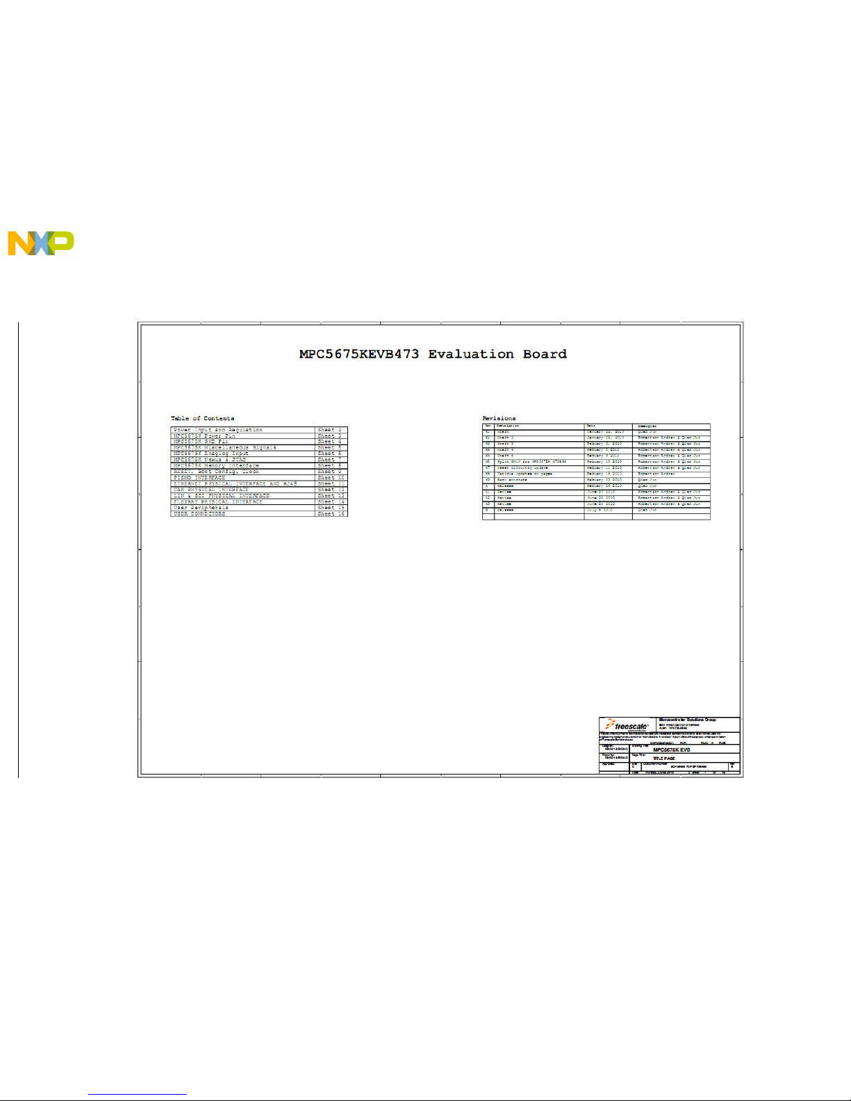
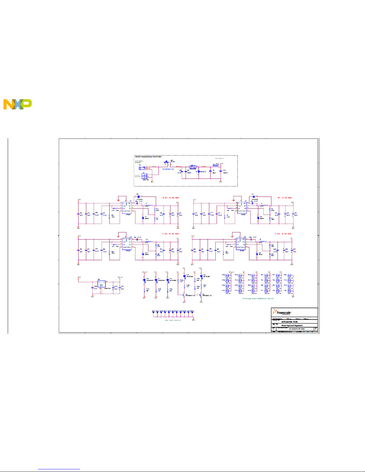
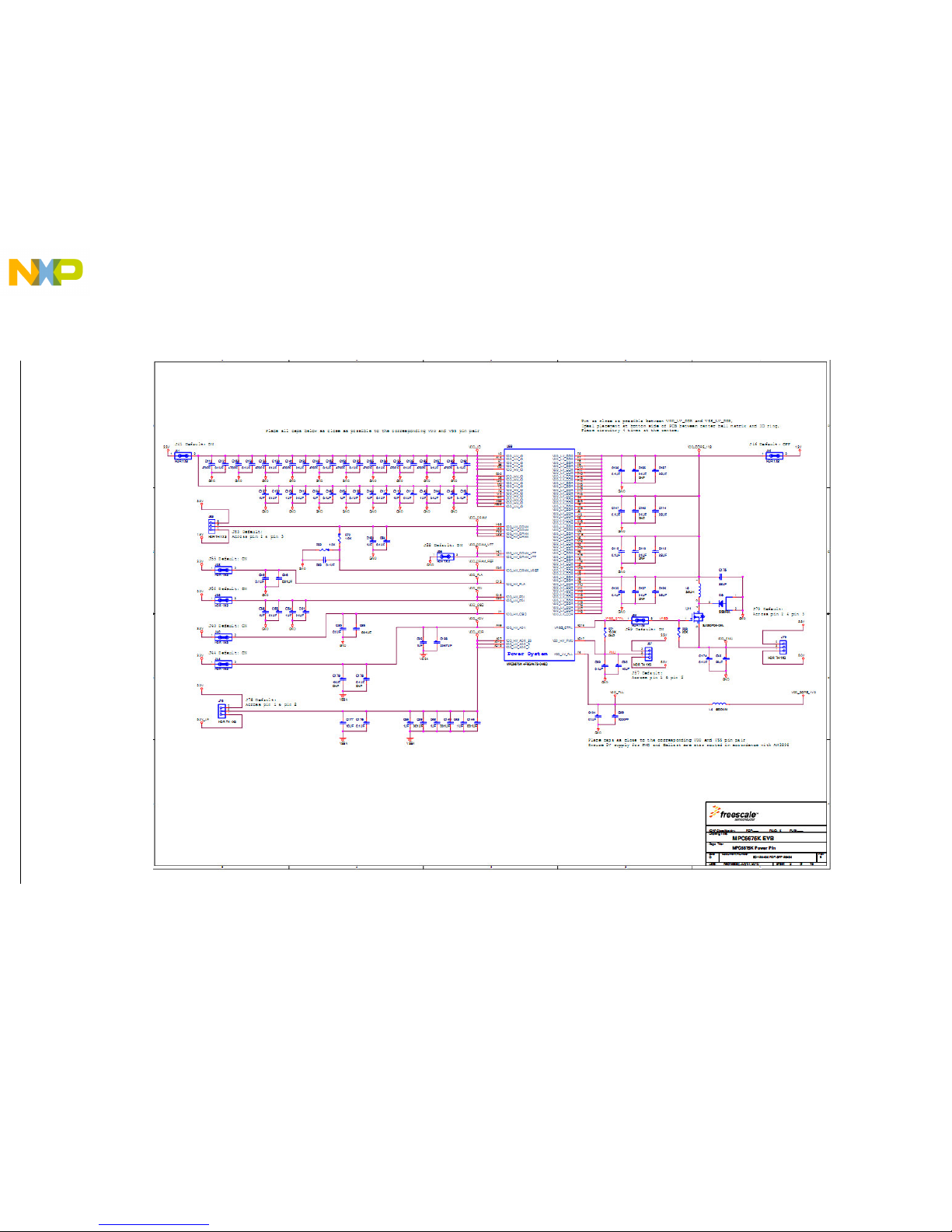
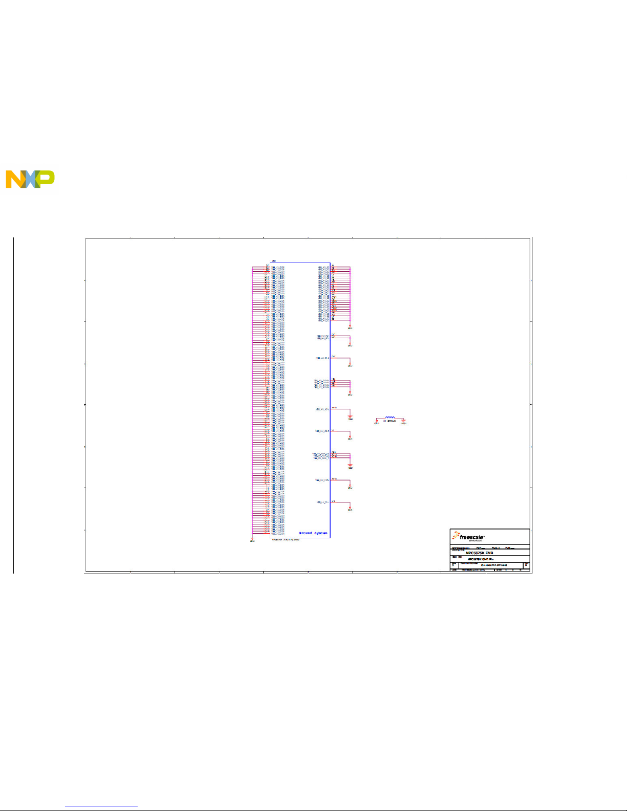
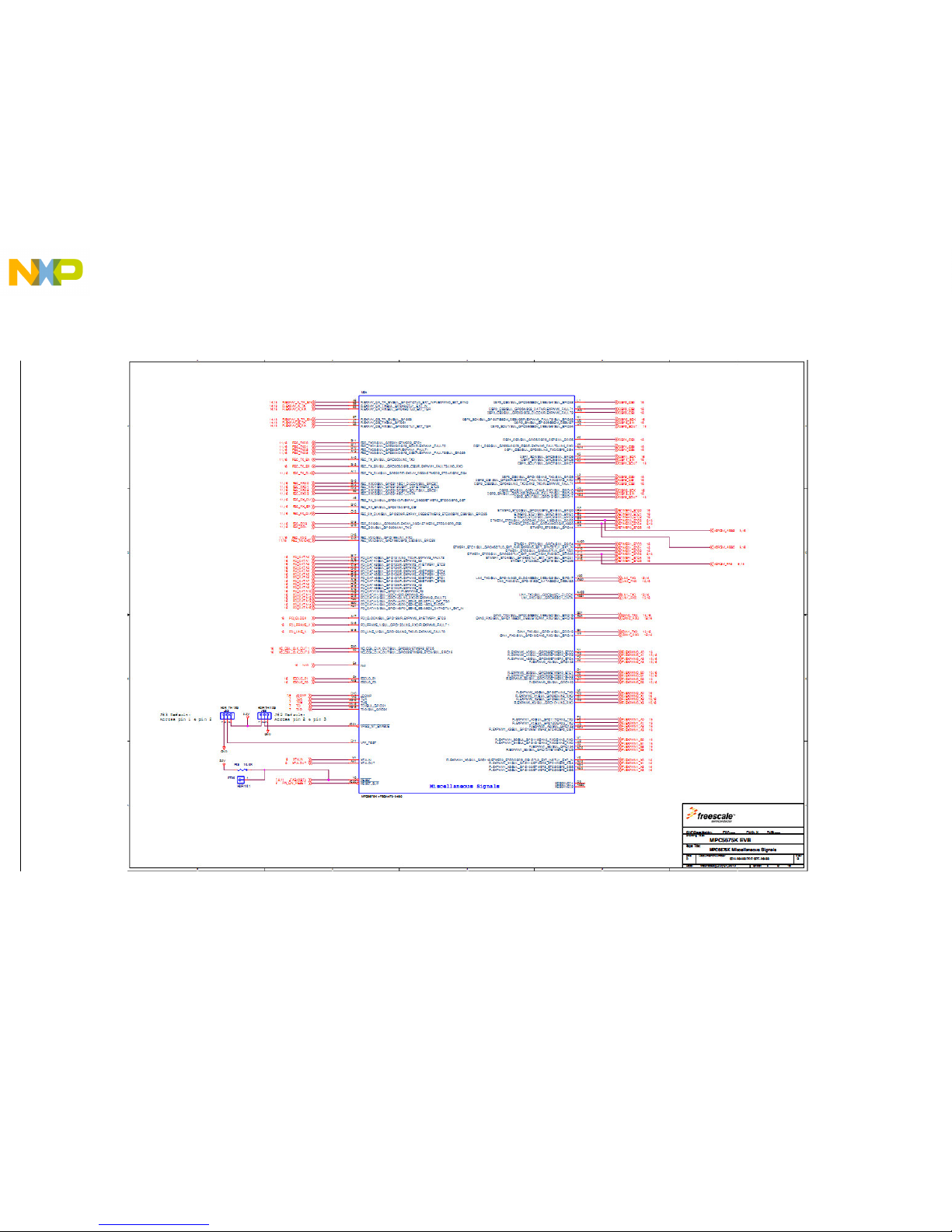
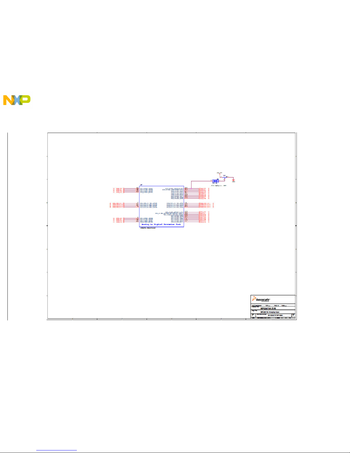
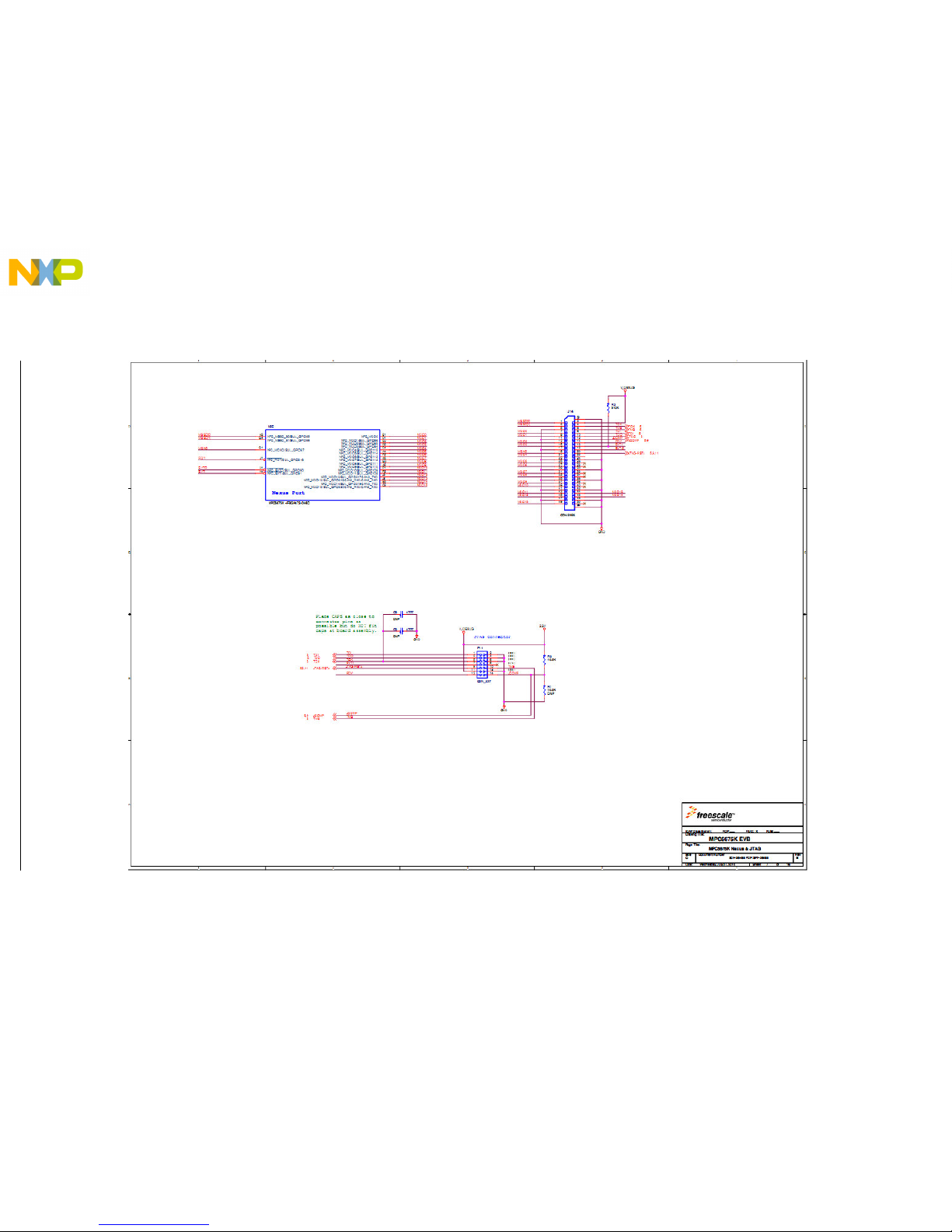
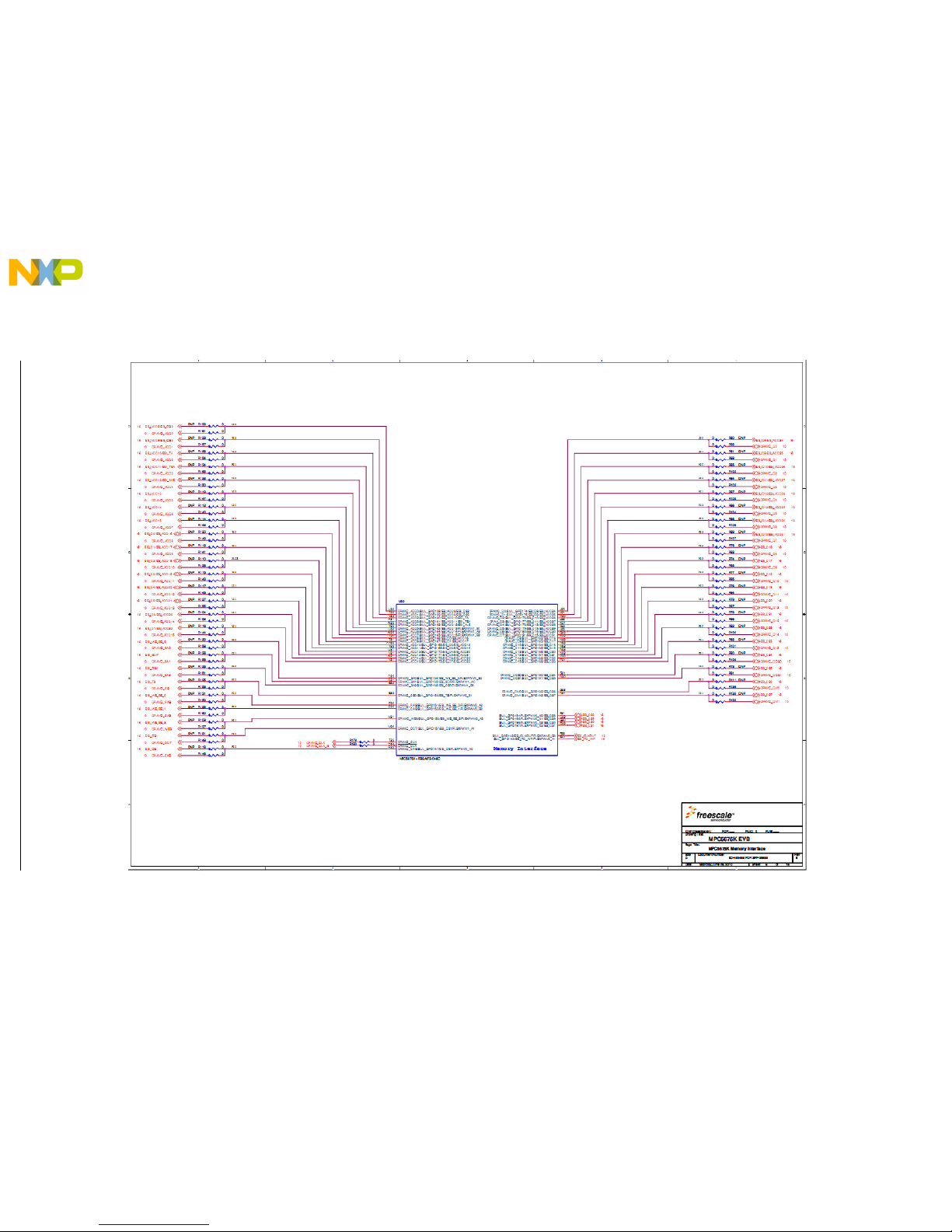
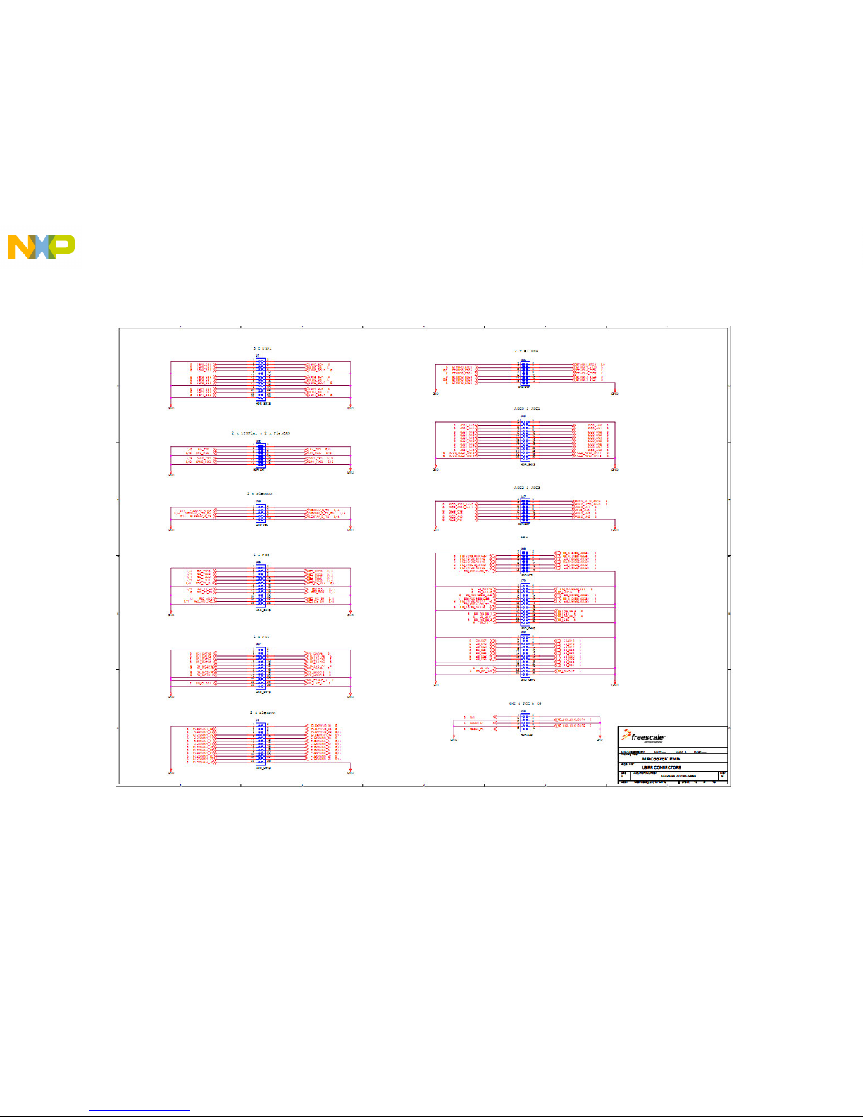
Appendix A - EVB Schematics
Page 30
MPC5675EVB Users Manual Rev 2.0 July 2010
MPC5675EVB Page A-2
Page 31
MPC5675EVB Users Manual Rev 2.0 July 2010
MPC5675EVB Page A-3
Page 32
MPC5675EVB Users Manual Rev 2.0 July 2010
MPC5675EVB Page A-4
Page 33
MPC5675EVB Users Manual Rev 2.0 July 2010
MPC5675EVB Page A-5
Page 34
MPC5675EVB Users Manual Rev 2.0 July 2010
MPC5675EVB Page A-6
Page 35
MPC5675EVB Users Manual Rev 2.0 July 2010
MPC5675EVB Page A-7
Page 36
MPC5675EVB Users Manual Rev 2.0 July 2010
MPC5675EVB Page A-8
Page 37
MPC5675EVB Users Manual Rev 2.0 July 2010
MPC5675EVB Page A-9
Page 38
MPC5675EVB Users Manual Rev 2.0 July 2010
MPC5675EVB Page A-10
Page 39
MPC5675EVB Users Manual Rev 2.0 July 2010
MPC5675EVB Page A-11
Page 40
MPC5675EVB Users Manual Rev 2.0 July 2010
MPC5675EVB Page A-12
Page 41
MPC5675EVB Users Manual Rev 2.0 July 2010
MPC5675EVB Page A-13
Page 42
MPC5675EVB Users Manual Rev 2.0 July 2010
MPC5675EVB Page A-14
Page 43
MPC5675EVB Users Manual Rev 2.0 July 2010
MPC5675EVB Page A-15
Page 44
MPC5675EVB Users Manual Rev 2.0 July 2010
MPC5675EVB Page A-16
Page 45
MPC5675EVB Users Manual Rev 2.0 July 2010
MPC5675EVB Page A-17
 Loading...