

Page 1
MPC5668EVB Users Manual
Revision 0.1
May 2009
Page 2

MPC5668EVB Users Manual Rev 0.1 May 2009
Revision
Date
Author
Comment
0.1 May 2009 D.
McMenamin
Initial Release, RevA PCB’s only
.
Revision History:
Information in this document is provided solely to enable system and software implementers to use
Freescale Semiconductor products. There are no express or implied copyright licenses granted
hereunder to design or fabricate any integrated circuits or integrated circuits based on the information
in this document. Freescale Semiconductor reserves the right to make changes without further notice
to any products herein. Freescale Semiconductor makes no warranty, representation or guarantee
regarding the suitability of its products for any particular purpose, nor does Freescale Semiconductor
assume any liability arising out of the application or use of any product or circuit, and specifically
disclaims any and all liability, including without limitation consequential or incidental damages.
“Typical” parameters that may be provided in Freescale Semiconductor data sheets and/or
specifications can and do vary in different applications and actual performance may vary over time. All
operating parameters, including “Typicals”, must be validated for each customer application by
customer’s technical experts. Freescale Semiconductor does not convey any license under its patent
rights nor the rights of others. Freescale Semiconductor products are not designed, intended, or
authorized for use as components in systems intended for surgical implant into the body, or other
applications intended to support or sustain life, or for any other application in which the failure of the
Freescale Semiconductor product could create a situation where personal injury or death may occur.
Should Buyer purchase or use Freescale Semiconductor products for any such unintended or
unauthorized application, Buyer shall indemnify and hold Freescale Semiconductor and its officers,
employees, subsidiaries, affiliates, and distributors harmless against all claims, costs, damages, and
expenses, and reasonable attorney fees arising out of, directly or indirectly, any claim of personal
injury or death associated with such unintended or unauthorized use, even if such claim alleges that
Freescale Semiconductor was negligent regarding the design or manufacture of the part.
Learn More: For more information about Freescale products, please visit www.freescale.com
Freescale™ and the Freescale logo are trademarks of Freescale Semiconductor.
All other product or service names are the property of their respective owners.
MPC5668EVBUM/D i
© Freescale Semiconductor, 2009; All Rights Reserved
Page 3

MPC5668EVB Users Manual Rev 0.1 May 2009
INDEX
1. INTRODUCTION ...................................................................................................................................................... 1
2. EVB FEATURES ...................................................................................................................................................... 2
3. CONFIGURATION ................................................................................................................................................... 3
3.1
P
OWER SUPPLY CONFIGURATION
3.1.1 Power Supply Connectors ........................................................................................................................ 4
3.1.2 Power Switch (SW6) .................................................................................................................................. 4
3.1.3 Regulator Power Jumpers (J42, J44, J45 and J46) .............................................................................. 5
3.1.4 Power Status LED’s and Fuse ................................................................................................................. 5
3.1.5 MCU Supply Routing and Jumpers (J41, J42, J43, J44, J45, J46, J47, J48, J49, J50)................. 6
3.1.6 Regulator Power Domains ........................................................................................................................ 8
3.2
MCU C
3.2.1 Main Clock Selection (J85, J87, J61 and J66) ....................................................................................... 9
3.2.2 32Khz External Clock Selection (J67 and J71).................................................................................... 10
3.3
R
3.3.1 Reset LEDs ............................................................................................................................................... 11
3.3.2 Reset Buffering Scheme ......................................................................................................................... 12
3.3.3 Reset Boot Configuration (J69) .............................................................................................................. 13
3.4
ONCE
3.4.1 Debug Connector Pinouts ....................................................................................................................... 14
3.5
CAN C
3.6
RS232 C
3.7
LIN C
J13, J14, J15,J16) ....................................................................................................................................................... 17
3.8
F
3.9
E
3.10
3.11 P
4. MCU PIN USAGE MAP ......................................................................................................................................... 24
LOCK CONTROL
ESET CONTROL (JUMPER
AND NEXUS CONFIGURATION
ONFIGURATION
ONFIGURATION
ONFIGURATION
LEX
RAY C
ONFIGURATION
THERNET
MLB
HANTOM PORTS
....................................................................................................................................................... 20
AND MOST
(J20, J21, J29, J30, J31) ......................................................................................... 15
(J3, J4, J5, J12,........................................................................................................... 17
.............................................................................................................................................. 21
(J76, J77, J78, J79, J80) ................................................................................................. 23
..................................................................................................................................... 9
(J6, J17, J18, J23, J24) ........................................................................................ 16
..................................................................................................................... 4
J75) ..................................................................................................................... 11
(J32, J70) .......................................................................................... 13
(J19, J27, J25, J26, J28) ................................................................................ 18
5. DEFAULT JUMPER SUMMARY TABLE .......................................................................................................... 25
6. USER CONNECTOR DESCRIPTIONS .............................................................................................................. 28
6.1.1 Port A / ADC (Connector J86, RV1, J73 and J74) .............................................................................. 28
6.1.2 Port B / ADC / SPI (P18) ......................................................................................................................... 29
6.1.3 Port C / ADC / FLEXRAY / I2C (P19) .................................................................................................... 29
6.1.4 Port D / CAN / I2C / SCI (P20) ............................................................................................................... 29
6.1.5 Port E / SCI / eMIOS / I2C (P21) ........................................................................................................... 30
6.1.6 Port F / DSPI (P26) .................................................................................................................................. 30
6.1.7 Port G / DSPI / eMIOS / FEC (P27)....................................................................................................... 30
6.1.8 Port H / eMIOS / FEC (P28) ................................................................................................................... 30
6.1.9 Port J / eMIOS / FEC (P29) .................................................................................................................... 31
6.1.10 Port K / RESET / MLB (Connector P30) .......................................................................................... 31
6.2
P
ROTOTYPING AREA AND USER
LED’S / S
WITCHES
...................................................................................... 32
APPENDIX A - SCHEMATICS
MPC5668EVBUM/D ii
Page 4

MPC5668EVB Users Manual Rev 0.1 May 2009
Index of Figures and Tables
F
IGURE
3-1
EVB F
F
IGURE
3-2
F
IGURE
3-3
F
IGURE
3-4. P
F
IGURE
3-5
F
IGURE
3-6
F
IGURE
3-7 EVB R
F
IGURE
3-8.
F
IGURE
3-9
F
IGURE
3-10
F
IGURE
3-11
F
IGURE
3-12.
F
IGURE
3-13.
T
ABLE
3-1
T
ABLE
3-2
T
ABLE
3-3
T
ABLE
3-4
T
ABLE
3-5
T
ABLE
3-6
T
ABLE
3-7
T
ABLE
3-8
T
ABLE
3-9
T
ABLE
3-10
T
ABLE
3-11
T
ABLE
3-12
T
ABLE
3-13.
T
ABLE
3-14
T
ABLE
3-15
T
ABLE
3-16
T
ABLE
3-17
T
ABLE
3-18
T
ABLE
3-19
T
ABLE
3-20
T
ABLE
3-21
T
ABLE
3-22 INIC P
T
ABLE
3-23 P
T
ABLE
4-1. EVB MCU P
T
ABLE
5-1
T
ABLE
6-1.
T
ABLE
6-2
T
ABLE
6-3.
T
ABLE
6-4.
T
ABLE
6-5.
T
ABLE
6-6.
T
ABLE
6-7.
T
ABLE
6-8.
T
ABLE
6-9.
T
ABLE
6-10.
T
ABLE
6-11.
UNCTIONAL BLOCKS
2.1
MM POWER CONNECTOR
2-L
EVER POWER CONNECTOR
OWER SUPPLY ROUTING
EVB C
LOCK SELECTION
EVB C
LOCK SELECTION
ESET BUFFERING SCHEME
MPC5668 JTAG / ONCE C
CAN P
HYSICAL INTERFACE CONNECTOR
RS232 P
LIN P
INC5668 JTAG C
MLB M
REGULATOR POWER JUMPERS
MCU P
VDDE[1..3] P
POWER SUPPLY DISTRIBUTION
CLOCK SOURCE JUMPER SELECTION
32K
LVI M
LVI C
RESET-OUT CONTROL JUMPER
BOOTCFG C
JTAG / NEXUS T
ONCE / NEXUS TCLK T
NEXUS D
CAN C
RS232 C
LIN C
FLEXRAY
FLEXRAY POWER CONTROL JUMPERS
FLEXRAY CONTROL JUMPERS
PULL UP/ PULL DOWN RESISTORS ON PORTS G AND H FOR ETHERNET PHYSICAL
EHTERNET PHYSICAL INTERFACE POWER SUPPLY ENABLED
HANTOM PORT CONTROL
DEFAULT JUMPER POSITIONS
PORT A CONNECTOR PINOUT
RV1 C
PORT B CONNECTOR PINOUT
PORT C CONNECTOR PINOUT
PORT D CONNECTOR PINOUT
PORT E CONNECTOR PINOUT
PORT F CONNECTOR PINOUT
PORT F CONNECTOR PINOUT
PORT H CONNECTOR PINOUT
PORT J CONNECTOR PINOUT
PORT K CONNECTOR PINOUT
HYSICAL INTERFACE CONNECTOR
HYSICAL INTERFACE CONNECTORS
ONITOR CONNECTOR
OWER SUPPLY JUMPERS
AD GROUPINGS
HZ CRYSTAL JUMPER SELECTION
ONITOR THRESHOLD VOLTAGES
ONTROL JUMPERS
ONTROL
ARGET RESET ROUTING
EBUG CONNECTOR PINOUT
ONTROL JUMPERS
ONTROL JUMPERS
ONTROL JUMPERS
MCU S
OWER SUPPLY CONTROL
ONNECTION JUMPER
IGNAL ROUTING JUMPERS
IN USAGE
............................................................................................................................ 3
.......................................................................................................................... 4
....................................................................................................................... 4
.............................................................................................................................. 6
................................................................................................................................. 9
............................................................................................................................... 10
................................................................................................................ 12
ONNECTOR
.................................................................................................... 14
.................................................................................................... 15
.............................................................................................. 16
.................................................................................................. 17
ONNECTOR
.................................................................................................................. 21
.................................................................................................................... 21
........................................................................................................................ 5
..................................................................................................................... 7
.......................................................................................................................... 8
........................................................................................................................ 8
.............................................................................................................. 9
........................................................................................................... 10
.......................................................................................................... 11
................................................................................................................................. 11
..................................................................................................................... 12
................................................................................................................................. 13
................................................................................................. 13
ERMINATION CONTROL
....................................................................................... 13
....................................................................................................... 14
(J30, J31, J7) .................................................................................................... 15
......................................................................................................................... 16
.............................................................................................................................. 17
(J19, J27) ............................................................................. 18
(J25) .............................................................................................. 18
(J26, J28) ................................................................................................... 19
................................... 20
(J26) ........................................................... 20
(J35, J36, J55) ........................................................................................ 21
(J35, J36, J55) .................................................................................................. 23
................................................................................................................................... 24
........................................................................................................................ 25
(P17) ............................................................................................................ 28
J8 ...................................................................................................................... 28
(P18) ............................................................................................................ 29
(P19) ............................................................................................................ 29
(P20) ............................................................................................................ 29
(P21) ............................................................................................................ 30
(P26) ............................................................................................................ 30
(P27) ............................................................................................................ 30
(P28) ........................................................................................................... 30
(P29) .......................................................................................................... 31
(P30) ......................................................................................................... 31
MPC5668EVBUM/D iii
Page 5

MPC5668EVB Users Manual Rev 0.1 May 2009
1. Introduction
This user’s manual details the setup and configuration of the Freescale Semiconductor MPC5668 Evaluation
Board (hereafter referred to as the EVB). The EVB is intended to provide a mechanism for easy customer
evaluation of the MPC5668 family of microprocessors, and to facilitate hardware and software development.
At the time of writing this document, the MPC5668 family is offered in a 208MAPBGA package. A
256MAPBGA package supporting Nexus debug is also available for development purposes. For the latest
product information, please speak to your Freescale representative or consult the MPC5668 web pages at
www.freescale.com
The EVB is intended for bench / laboratory use and has been designed using normal temperature specified
components (+70°C).
MPC5668EVBUM/D Page 1 of 29
Page 6

MPC5668EVB Users Manual Rev 0.1 May 2009
IMPORTANT
2. EVB Features
The EVB provides the following key features:
• MCU Socket supporting the 208BGA production package and the 256BGA development package.
• Single 12-14V external power supply input with on-board regulators to provide all of the necessary
EVB and MCU voltages. Power may be supplied to the EVB via a 2.1mm barrel style power jack or a
2-way level connector. 12V operation allows in-car use if desired.
• Flexible on-board power supply configuration with the option to bypass the internal MCU regulators if
desired.
• Master power switch and regulator status LED’s – Regulators connected to the ADC to allow
monitoring.
• User reset switch with reset status LED’s
• User configurable Low Voltage Inhibit to monitor the status of the 3.3V and 5V regulators.
• Control of the BOOTCFG status via a dedicated jumper.
• Flexible MCU clocking options:
40MHz Oscillator Crystal
32Khz Watch Crystal
SMA connector to allow external clock support
8Mhz Oscillator circuit.
• SMA connector on MCU-CLKOUT signal for easy access.
• Standard 14-pin ONCE debug connector and 38-pin MICTOR Nexus connectors.
• All MCU signals are accessible on port-ordered groups of 0.1” pitch headers.
• DSPI A signals can be routed to a set of shift registers to allow a 32-bit phantom port to be created.
• SCI channels A and B can be routed to a standard DB9 female connector (PC RS-232 compliant) via
a Maxim physical interface.
• SCI channels C and D can be routed to LIN interface header (0.1”) and molex connectors, both will
full physical transceivers.
• FlexCAN channels A and B can be routed to 0.1” headers and DB9 connector via a Philips high speed
CAN transceiver which supports both 3.3V and 5V inputs.
• FlexCAN channels C, D, E and F are routed to the prototyping area with DB9 connectors to allow
additions CAN physical interfaces to be easily integrated.
• User prototyping area consisting of a 0,1” grid of through hole pads with easy access to the EVB
ground and power supply rails.
• Ethernet signals routed to a National Semiconductor physical interface and Pulsejack RJ45 connector
with integrated magnetics.
• MLB signals routed to SMSC MOST INIC with Tyco Optical Transceiver. INIC JTAG and MLB monitor
ports. Support for optional ROM INIC or MLB150 daughter card from SMSC.
• 4 active low LED’s and 4 pushbutton switches for development purposes.
• Jumper selectable variable resistor connected to ADC channel 0, driving between VRH and VRL.
• Liberal scattering of GND test points (surface mount loops) placed throughout the EVB.
Note – To alleviate confusion between jumpers and headers, all EVB jumpers are implemented as 2mm pitch
whereas headers are 0.1inch (2.54mm). This prevents inadvertently fitting a jumper to a header.
Before the EVB is used or power is applied, please fully read the following
sections on how to correctly configure the board.
Failure to correctly configure the board may cause irreparable component, MCU or EVB
damage.
MPC5668EVBUM/D Page 2 of 29
Page 7
MPC5668EVB Users Manual Rev 0.1 May 2009
User LEDs and
Connectors
Regulators
JTAG and
Connectors
Jumpers
Reset and
Port
Ethernet
3. Configuration
This section details the configuration of each of the EVB functional blocks.
Throughout this document, all of the default jumper and switch settings are clearly marked with “(D)” and are
shown in blue text. This should allow a more rapid return to the default state of the EVB if required. Note that
the default configuration for 3-way jumpers is a header fitted between pins 1 and 2. On the EVB, 2-way and 3way jumpers have been aligned such that Pin 1 is either to the top or to the left of the jumper. On 2-way
jumpers, the source of the signal is connected to Pin 1.
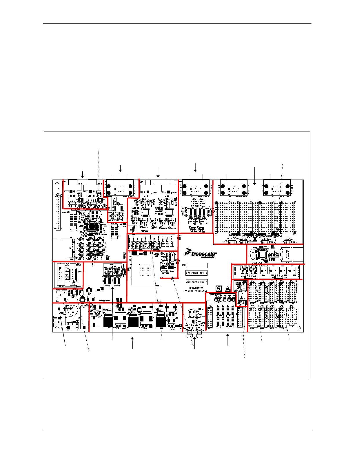
The EVB has been designed with ease of use in mind and has been segmented into functional blocks as
shown below. Detailed silkscreen legend has been used throughout the board to identify all switches, jumpers
and user connectors.
MOST and MLB
LIN
Serial (SCI)
Flexray
CAN
Prototype
Area
MCU
Socket
Power Routing
Power
NEXUS
LVI
Voltage
Clock
Circuitry and
SMA In / Out
Phantom
Potentiometer
switches
User
User
Figure 3-1 EVB Functional Blocks
MPC5668EVBUM/D Page 3 of 29
Page 8
MPC5668EVB Users Manual Rev 0.1 May 2009
3.1 Power Supply Configuration
The Power supply
section is located in
the bottom left area
of the EVB
The EVB requires an external power supply voltage of 12V DC, minimum 1A. This allows the EVB to be easily
used in a vehicle if required. The single input voltage is regulated on-board using 3 switching and 1 linear
regulators to provide the necessary EVB and MCU operating voltages of 5.0V, 3.3V and 2.5V. For flexibility
there are two different power supply input connectors on the EVB as detailed below.
3.1.1 Power Supply Connectors
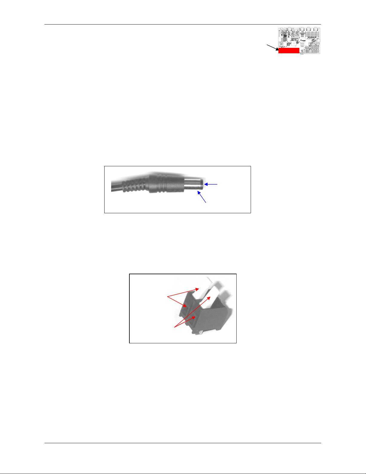
2.1mm Barrel Connector – P22:
This connector should be used to connect the supplied wall-plug mains adapter. Note – if a replacement or
alternative adapter is used, care must be taken to ensure the 2.1mm plug uses the correct polarisation as
shown below:
Figure 3-2 2.1mm Power Connector
2-Way Lever Connector – P23:
This can be used to connect a bare wire lead to the EVB, typically from a laboratory power supply. The
polarisation of the connectors is clearly marked on the EVB. Care must be taken to ensure correct connection.
V+ (12V)
GND
Figure 3-3 2-Lever Power Connector
V+ (12V)
GND
3.1.2 Power Switch (SW6)
Slide switch SW6 can be used to isolate the power supply input from the EVB voltage regulators if required.
Moving the slide switch to the right (away from connector P23) will turn the EVB on.
Moving the slide switch to the left (towards connector P23) will turn the EVB off.
MPC5668EVBUM/D Page 4 of 29
Page 9

MPC5668EVB Users Manual Rev 0.1 May 2009
Jumper
Position
PCB
Description
(D)
(D)
(D)
(D)
3.1.3 Regulator Power Jumpers (J42, J44, J45 and J46)
The Power supply control jumpers are located adjacent to the respective regulators.
As mentioned above, the EVB has four voltage regulators on board:
- 2.5V switching regulator (U17) to supply the MCU MLB Pads voltage and the SMSC INIC (U6).
- 3.3V switching regulator (U18) for EVB peripherals and MCU regulator, logic and I/O.
- 5.0V switching regulator (U19) for the MCU regulator and I/O and EVB peripherals.
- 5.0V linear regulator (U14) for the MCU ADC power supply.
All of the regulators have the option of being disabled if they are not required. The table below details the
jumper configurations for enabling and disabling the regulators. By default, all of the regulators are enabled.
Table 3-1 Regulator Power Jumpers
Legend
J81 (2.5V)
J82 (3.3V)
J83 (5.0V)
J84 (5.0V-LINEAR)
FITTED
REMOVED
FITTED
REMOVED
FITTED
REMOVED
FITTED
REMOVED 5.0V linear regulator output is Disabled
DISABLE
DISABLE
DISABLE
ENABLE 5.0V linear regulator output is Enabled
2.5V switching regulator output is
Disabled
2.5V switching regulator output is
Enabled
3.3V switching regulator output is
Disabled
3.3V switching regulator output is
Enabled
5.0V switching regulator output is
Disabled
5.0V switching regulator output is
Enabled
3.1.4 Power Status LED’s and Fuse
When power is applied to the EVB, four green power LED’s adjacent to the voltage regulators show the
presence of the supply voltages as follows:
LED DS8 – Indicates that the 5.0V linear regulator is enabled and working correctly
LED DS9 – Indicates that the 1.5V switching regulator is enabled and working correctly
LED DS10 – Indicates that the 3.3V switching regulator is enabled and working correctly
LED DS11 – Indicates that the 5.0V switching regulator is enabled and working correctly
If no LED’s are illuminated when power is applied to the EVB and the regulators are correctly enabled using
the appropriate jumpers, it is possible that either power switch SW6 is in the “OFF” position or that the fuse F1
has blown. The fuse will blow if power is applied to the EVB in reverse-bias, where a protection diode ensures
that the main fuse blows rather than causing damage to the EVB circuitry. If the fuse has blown, check the
bias of your power supply connection then replace fuse F1 with a 20mm 500mA fast blow fuse.
MPC5668EVBUM/D Page 5 of 29
Page 10
MPC5668EVB Users Manual Rev 0.1 May 2009
jumpers are located in the
centre of the EVB in a box
MCU Powe
The MCU power supply
3.1.5 MCU Supply Routing and Jumpers
(J41, J42, J43, J44, J45, J46, J47, J48, J49,
titled “MCU Supply”
J50)
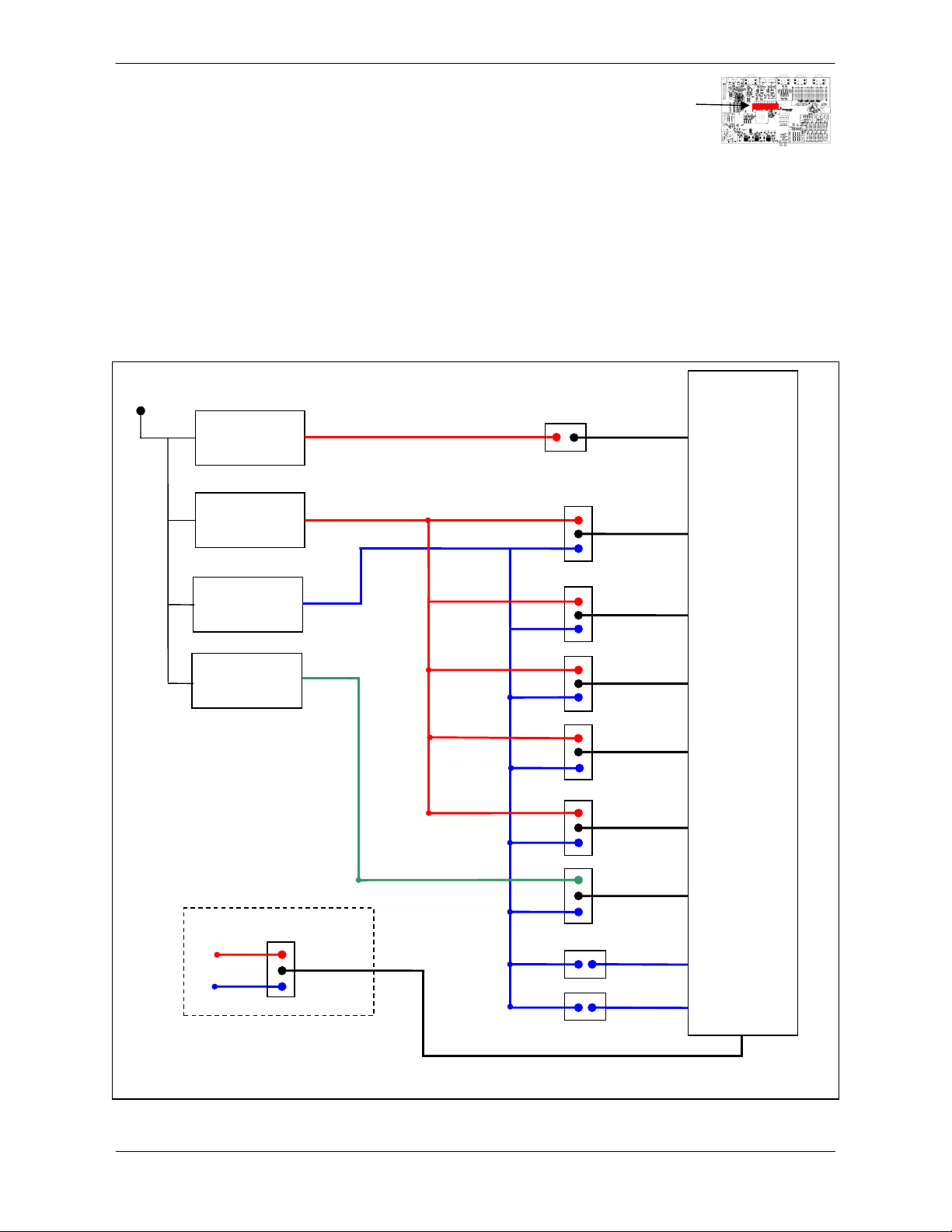
The MCU can be operated in 5v and 3.3v modes by changing J46. When in 5v mode MCU has internal
regulators that can generate the 3.3V supplies for VDDSYN and VDD33. Whilst this is the intended mode of
operation for the MCU when VRC = 5v the EVB allows the internal MCU regulators to be disabled by
changing VRCSEL to EXT and applying external voltages to the VDDSYN and VDD33 inputs. When in 3.3v
mode VDDSYN and VDD33 inputs must always be supplied externally.
The VDDE[1..4] pins control the pad voltages over 4 groupings of pads (see the MCU reference manual for
details). Jumpers J41 - J34 allow the VDDEx pins to be connected to the 5.0v or 3.3V switching regulators.
The VDDEMLB domain can be 3.3v or 2.5v selectable by J45.
12V
5V Linear
5V Switcher
J49
1
VDDA
J46
1
VRC
r
3.3V
Switcher
2.5V
Switcher
VRCSEL
1
0
1
J43
VDDE1
1
J42
VDDE2
1
J44
VDDE3
1
J41
VDDE4
1
J45
VDDEMLB
J47
1
INTernal
J50
1
VDDSYN
EXTernal
1
VDD33
J48
MPC5668EVBUM/D Page 6 of 29
VRCSEL
Figure 3-4. Power Supply Routing
Page 11

MPC5668EVB Users Manual Rev 0.1 May 2009
(D)
5.0V /
J46
(D)
J47
(D)
J43
(D)
J42
(D)
J44
(D)
J41
(D)
J48
J50
3.3v/
J45
(D)
CAUTION
Table 3-2 MCU Power Supply Jumpers
Power
Domain
5.0V J49 (VDDA)
3.3V
Jumper Position PCB
FITTED
REMOVED MCU VDDA User powered from J49 Pin 2
1-2
(VRC)
Description
Legend
MCU VDDA is powered from 5V linear regulator
5V VRC is supplied from the 5V switching regulator
2-3 3.3v VRC is supplied from the 3.3V switching regulator
1-2
(VRCSEL)
INT 3.3 V internal voltage regulator enabled (5 V mode)
2-3 EXT 3.3 V supplied external (3.3 V mode)
1-2
(VDDE1)
5.0v MCU VDDE1 is powered from 5v
2-3 3.3V MCU VDDE1 is powered from 3.3V
1-2
(VDDE2)
5.0v MCU VDDE2 is powered from 5v
2-3 3.3V MCU VDDE2 is powered from 3.3V
3.3V
2.5V
(VDDE3)
(VDDE4)
(VDD33)
(VDDSYN)
(VDDEMLB)
2-3
1-2
2-3
FITTED MCU VDD33 pin is powered from switching regulator
REMOVED
(D)
FITTED MCU VDDSYN pin is powered from switching
REMOVED
(D)
1-2
2-3 3.3V MCU VDD pin is not powered externally
5.0v MCU VDDE3 is powered from 5v
3.3V MCU VDDE3 is powered from 3.3V
5.0v MCU VDDE4 is powered from 5v
3.3V MCU VDDE4 is powered from 3.3V
MCU VDD33 pin is not powered externally
regulator
MCU VDDSYN pin is not powered externally
2.5V MCU VDD pin is powered from 1.5v switching
regulator
1-2
The jumper configuration shown in Table 3-2, details the default state of the EVB. In this configuration all
power is supplied from the Linear and Switching regulators.
- VDDA is connected to the 5.0V Linear regulator
- VRC is connected to the 5.0V switching regulator
- VRCSEL is connected to logic 1 enabling the internal 3.3V regulator – J48 and J50 are removed.
- VDDE[1..4] are connected to the 5.0V switching regulator
When jumper J47 (VRCSEL) is in position 1-2 (INT), the MCU’s 3.3V internal voltage regulators are
enabled and supply power to the 3.3V power domains. In this case, jumpers J48 (VDD33) and J50
(VDDSYN) must be removed.
Similarly, when jumper J47 is removed, no power is supplied to the MCU internal voltage regulators and
jumpers J48 (VDD33) and J50 (VDDSYN) must be fitted to power the respective MCU pins. The 3.3V
regulator must also be enabled in this case.
MPC5668EVBUM/D Page 7 of 29
Page 12
MPC5668EVB Users Manual Rev 0.1 May 2009
Ethernet
Port G and H
VDDE
3 3.3V
Nexus
Custom Domain
VDDE
NEX 3.3V
Regulator
Used On
2
.5V
3.3V
5.0V
5.0V
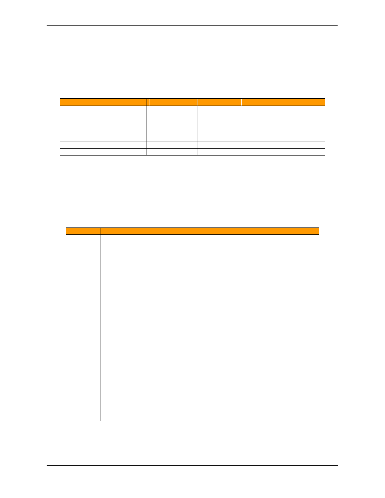
3.1.5.1 Changing VDDE[1..4] Voltage
Before changing the VDDEx voltage from the default 5.0V setting, you need to ensure that this will not impact
any of the EVB peripherals that you are using. The table below details what EVB peripherals are tied to a
particular VDDEx grouping and also the MCU pin operating voltage suitable for that peripheral.
Table 3-3 VDDE[1..3] Pad Groupings
Item Port Pins VDDE Group Required Pad Voltage
CANA and CANB Port D VDDE2 5.0V or 3.3V
SCI A and B Port D VDDE2 5.0V or 3.3v
LIN C and D Port E VDDE2 5.0V or 3.3v
FlexRay Port K VDDE2 5.0V or 3.3V
JTAG Dedicated JTAG VDDE2 5.0V or 3.3V
3.1.6 Regulator Power Domains
Before disabling any of the EVB regulators, it is worthwhile considering if any of the EVB components or
peripherals you require will be affected. Table 3-4 details a list of the various EVB components and
peripherals powered by the regulators.
Table 3-4 Power Supply Distribution
MCU VDDEMLB pins
(Switcher)
MLB INIC
1.5V Power section of Prototype area
MCU VDD33 and VDDSYN pins (ONLY use when on-chip MCU regulator is
(Switcher)
disabled)
MCU VDDEx pins (when run in 3.3v mode)
Oscillator Module (U20)
MLB INIC
RS-232 Transceiver (VDDE2 dependant)
LIN transceiver (VDDE2 dependant)
I/O supply for Flexray interface when VIO is 3.3V
LVI circuitry
3.3V Power section of Prototype area
MCU VDDEx (5v mode), VPP and VDDR pins
(Switcher)
LVI circuit main power (affecting Reset Switch)
Reset-In / Reset-Out logic
Reset configuration circuitry
User LED’s and Switches.
RS-232 Transceiver (VDDE2 dependant)
LIN transceiver (VDDE2 dependant)
CAN transceivers
FlexRay transceivers
5.0V Power section of Prototype area
JTAG and Nexus connectors
MCU VDDA pin
(Linear)
LVI circuit monitor
MPC5668EVBUM/D Page 8 of 29
Page 13
MPC5668EVB Users Manual Rev 0.1 May 2009
Jumper
Position
PCB
Description
(D)
(D)
(D)
(D)
MCU
3.2 MCU Clock Control
The MCU clock
control jumpers are
located close to
crystal oscillator
modules.
3.2.1 Main Clock Selection (J85, J87, J61 and J66)
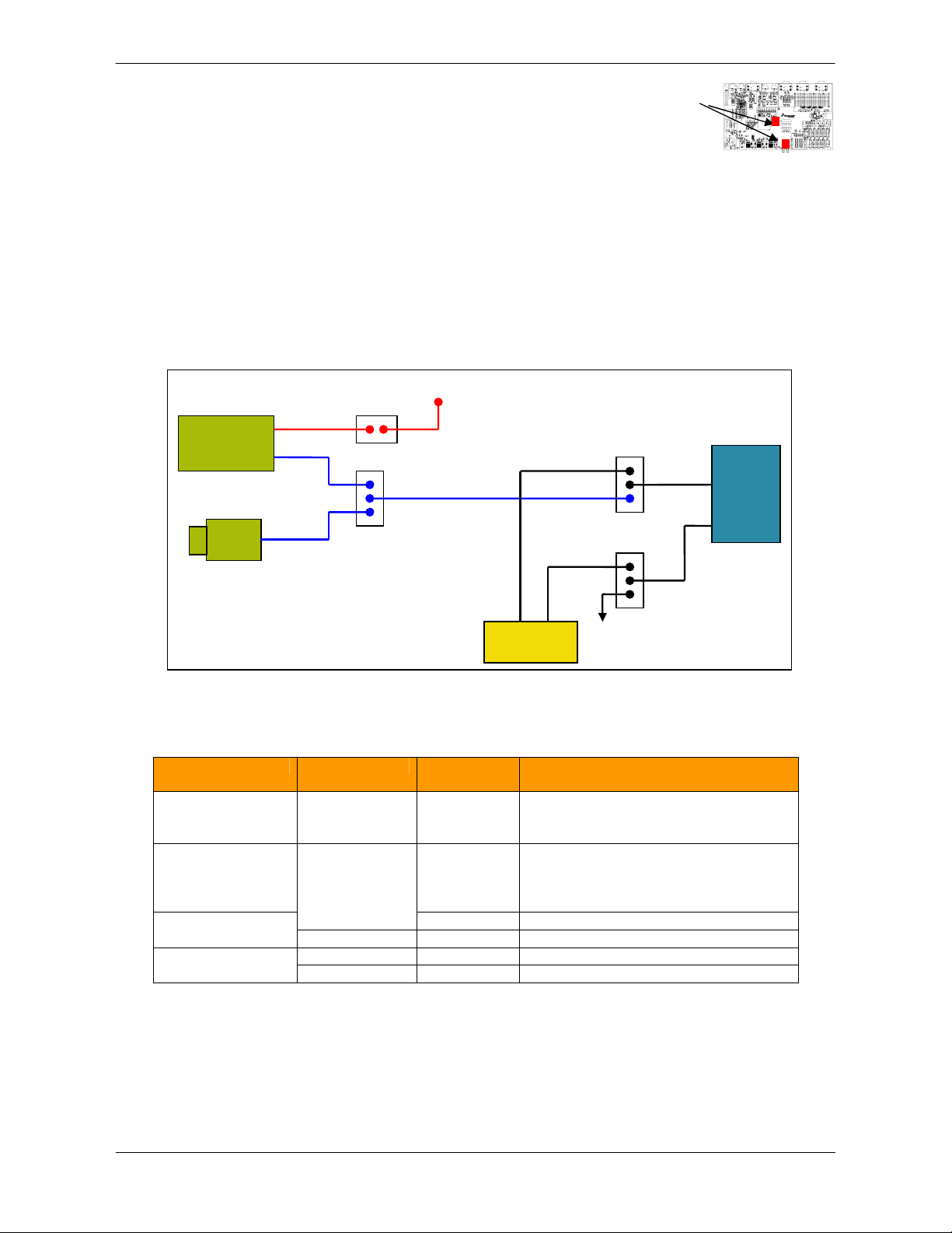
The EVB supports three possible MCU clock sources:
(1) The local 40MHz ALC pierce oscillator circuit
(2) An oscillator module on the EVB (U20), driving the MCU EXTAL signal
(3) An external clock input to the EVB via the SMA connector (P32), driving the MCU EXTAL signal
The clock circuitry is shown in the diagram below. Please refer to the appropriate daughter card user manual
for specific jumper numbers and circuitry.
Oscillator
Module
(U20)
J85
J87
SMA
(P32)
Figure 3-5 EVB Clock Selection
Table 3-5 Clock Source Jumper Selection
3.3V_SR
Local Crystal
Circuit (Y2)
1
1
GND
EVB Clock Circuitry
J66
EXTAL
XTAL
J61
Legend
J85 (U20 PWR)
J87 (OSC SEL)
J66
Must Match J61
J61
Must Match J66
FITTED
REMOVED
1-2
2-3
1-2
2-3 GND MCU Clock is Selected by J87
1-2
2-3 EVB MCU Clock is Selected by J87
EVB oscillator module U20 is powered
MOD
SMA
Y2 MCU Clock is Y2
Y2 MCU Clock is Y2
EVB oscillator module U20 is not
powered
Daughter card EXT-CLK is routed from
U20
Daughter card EXT-CLK is routed from
P32 SMA Connector
Note that the 3.3V regulator must be enabled when using oscillator module Y1.
CAUTION
The MPC5668 clock circuitry is all 3.3v based. Any external clock signal driven into the SMA connector must
have a maximum voltage of 3.3V.
MPC5668EVBUM/D Page 9 of 29
Page 14
MPC5668EVB Users Manual Rev 0.1 May 2009
Jumper
Position
PCB
Description
(
D)
(D)
MCU
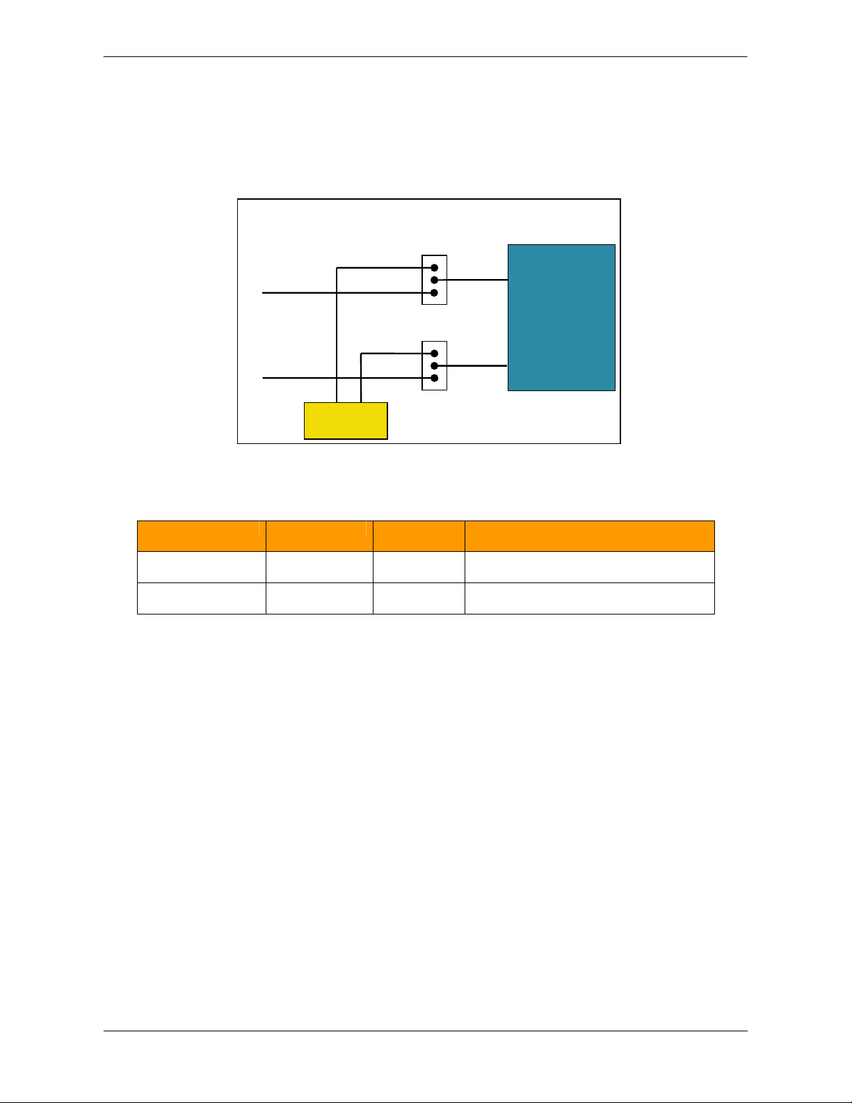
3.2.2 32Khz External Clock Selection (J67 and J71)
The EVB also supports an external 32KHz watch crystal that can be used as a timing source within the MCU.
The 32Khz crystal can be optionally connected to PA[14] and PA[15] of the MCU. When using the 32KHz
crystal PA[14] and PA[15] will not be visible on P17 Port A header.
PA[14]
PA[15]
32Khz Crystal
Circuit (Y3)
Figure 3-6 EVB Clock Selection
Table 3-6 32Khz Crystal Jumper Selection
32KHz EVB Clock Circuitry
J67
1
J71
1
EXTAL32 / PA[14]
XTAL32 / PA[15]
J67
Must Match J71
J71
Must Match J67
Legend
1-2
Y3 32Khz Crystal (Y2) is connected to MCU
2-3 PA[14] Pin functions as Normal I/O
1-2
2-3
Y3 32Khz Crystal (Y2) is connected to MCU
PA[15]
Pin functions as Normal I/O
MPC5668EVBUM/D Page 10 of 29
Page 15
MPC5668EVB Users Manual Rev 0.1 May 2009
Regulator
Minimum Voltage Before
MCU
Jumper
Position
PCB Legend
Description
(D)
(D)
3.3 Reset Control (Jumper J75)
The RESET switch (RED)
and LVI circuitry is located
to the t left of the MCU in
the area titled “RESET “
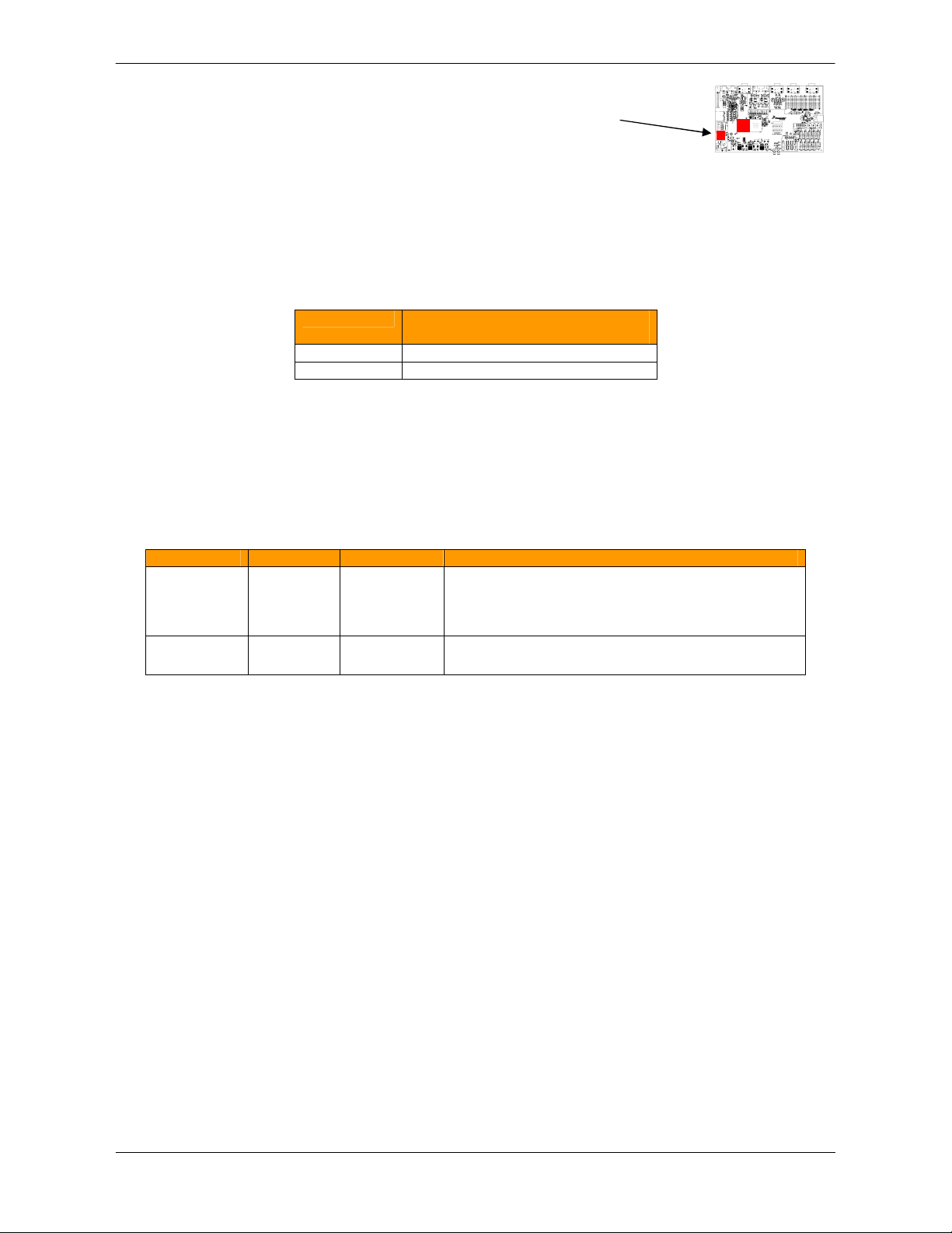
The EVB incorporates an LVI (Low Voltage Inhibit) device to provide under-voltage protection for the two main
switching regulators (5v and 3.3v). When either of these regulator voltages drops below a certain threshold
level, the LVI will assert the MCU reset line to prevent incorrect operation of the MCU (or EVB circuitry).
The table below shows the approximate threshold voltages for each regulator
Table 3-7 LVI Monitor Threshold Voltages
reset
5.0V Switcher 1.47V
3.3V Switcher 1.47V
The LVI is powered from the 5.0V switching regulator and monitors the 3.3V regulator using a 2nd power fail
monitor circuit. The LVI also provides a de-bounced input for EVB reset switch SW5.
Jumpers are provided to disable either the main LVI reset out (which affects the reset from the 5.0V switching
regulator and from the reset switch) or the power fail out circuit (which only affects the reset from the 3.3V
regulator). If the 5v regulator LVI is disabled, the reset switch will not function.
Table 3-8 LVI Control Jumpers
J75
Posn 1-2
FITTED
REMOVED
5.0V switching regulator is monitored, Reset switch
active
5.0V switching regulator is not monitored, Reset
switch inactive
J75
Posn 3-4
FITTED
REMOVED
3.3V switching regulator is monitored
3.3V switching regulator is not monitored
Notes:
- If the 5.0V switching regulator is disabled for any reason, the LVI circuit will attempt to assert the MCU
Reset signal. Jumper shunts on jumper J20 position 1-2 and 3-4 must be removed in this situation.
This will also leave the reset switch SW5 inoperative.
- If the 3.3V regulator is disabled, the shunt on jumper J20 position 3-4 must be removed to prevent the
LVI asserting reset.
3.3.1 Reset LEDs
There are two reset LED’s, DS2 (AMBER) and DS3 (RED), placed adjacent to the EVB RESET switch to
indicate the RESET status of the EVB and MCU.
LED DS3, titled “RST”, will illuminate if the MCU itself issues a reset. In this condition, LED DS2 will not
illuminate.
LED DS2, titled “USR”, will illuminate when one of the following external hardware devices issues a reset to
the MCU:
- LVI circuitry (either an under-voltage detection or the reset switch is being pressed)
- There is a reset being asserted from the user connectors or from the daughter card
- There is a reset being driven from the Nexus or JTAG debug probe
Note that LED DS3 (MCU Reset) will also illuminate during an external (user) reset!
MPC5668EVBUM/D Page 11 of 29
Page 16
MPC5668EVB Users Manual Rev 0.1 May 2009
Jumper
Position
PCB Legend
Description
(D)
MCU
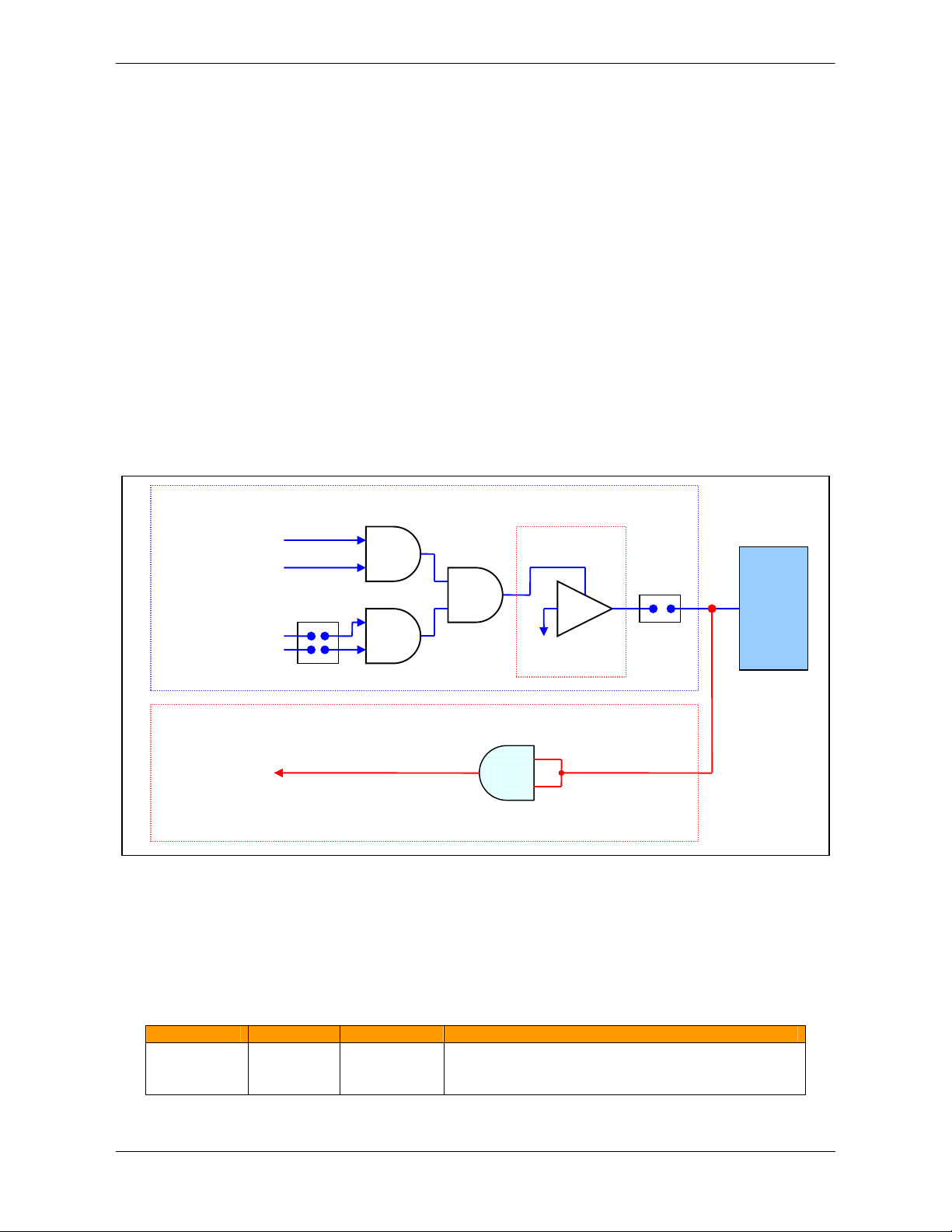
3.3.2 Reset Buffering Scheme
The MPC5668 family has a single reset pin. This single pin functions as a dual purpose input / output signal,
providing Reset-In and Reset-Out functionality.
There is a lot of circuitry on the EVB that has access to the reset pin. In order to reduce the loading on the pin
(when the MCU is diving the reset signal) and also to allow connection of non open-drain reset inputs, a resetin and reset-out buffering scheme is implemented as shown in Figure 3-7.
Reset-In - There are 3 possible external sources of reset:
- JTAG / Nexus connector reset
- User reset (from user connectors)
- LVI reset circuitry, including the reset switch.
Each of these reset sources is fed into the input of an AND gate and then converted to an opendrain output which is directly connected to the MCU reset pin.
Reset-Out - The MCU reset pin is buffered to provide a reset-out signal, capable of driving the reset LED and
also multiple devices requiring a reset input.
The reset buffering scheme is detailed below:
Reset IN
From JTAG / Nexus
From TGT
From LVI (5v)
From LVI (3.3v)
J75
Tri State Buffer
GND
J68
RESET
Reset OUT
Reset OUT
(To RED Reset LED, BDM Reset In,
external device reset)
Figure 3-7 EVB Reset Buffering Scheme
Jumper J17 is used to completely disconnect the reset-in buffering if desired. This is for debug purposes only
and should normally be left connected. Disconnecting this jumper will mean no external MCU reset can be
achieved
Table 3-9 Reset-Out Control Jumper
J68
(RST-IN)
MPC5668EVBUM/D Page 12 of 29
FITTED
REMOVED
External reset source (LVI, Debug or Target) will be
able to assert MCU reset
External reset is disabled (Not recommended)
Page 17
MPC5668EVB Users Manual Rev 0.1 May 2009
Jumper
Position
PCB Legend
Descr
iption
(D)
Jumper
Position
PCB Legend
Description
(D)
Jumper
Position
PCB Legend
Description
(D)
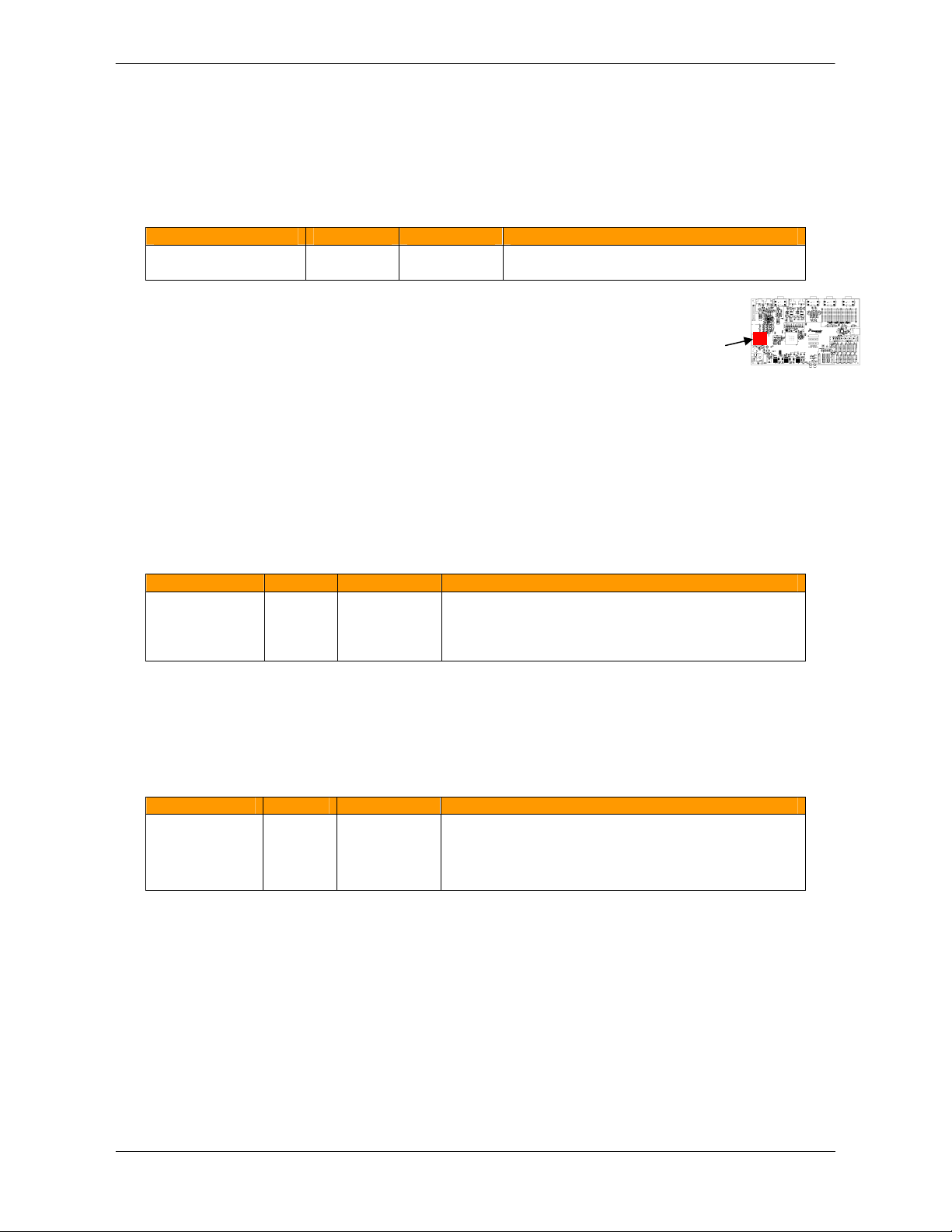
3.3.3 Reset Boot Configuration (J69)
The MPC5668 has a single boot configuration pin (BOOTCFG) which determines the boot location of the
MCU based on the state of the pin at POR (Power On Reset). This is shown in the table below:
Table 3-10 BOOTCFG Control
1-2
J69 (BOOT CFG)
2-3 SERIAL MCU boots from external serial source
3.4 ONCE and Nexus Configuration (J32, J70)
ON
The EVB supports a standard ONCE cable with a 14-pin 0.1” walled header footprint. There is also a 38-pin
MICTOR connector for Nexus debug. Nexus debug is only supported when using a 256MAPBGA MPC5668.
There are two generic jumpers associated with both the ONCE and Nexus, as detailed below
Some debug probes have the ability to assert and also monitor the state of the MCU reset line. This is not
possible when the reset signal is buffered so a jumper (J32) is included to allow routing the debug reset signal
direct to the MCU reset pin or via the EVB Reset-In buffering.
Table 3-11 JTAG / NEXUS Target Reset Routing
FLASH MCU boots from internal flash
The ONCE and NEXUS
connectors are located at
the left hand edge of the
1-2
J32 (JRST)
2-3
BUF
DIR
JTAG reset signal is buffered to MCU RESET pin
(connected to the MCU Reset-In circuitry)
JTAG reset signal is connected direct to MCU
RESET pin
Some debug manufacturers specify whether the debug TCLK signal is pulled low or high. Jumper J70
provides the ability to select whether TCLK is pulled to GND or VDDE2. For low power operation, TCLK
should be pulled to GND.
Table 3-12 ONCE / NEXUS TCLK Termination Control
1-2
J70
(TCLK PULL)
2-3
VDDE2
GND
JTAG / NEXUS TCLK signal is pulled to VDDE2 via
10KΩ
JTAG / NEXUS TCLK signal is pulled to GND via
10KΩ
Note – J70 is located to the right of the reset LED’s, out-with the ONCE / Nexus connector area.
MPC5668EVBUM/D Page 13 of 29
Page 18
MPC5668EVB Users Manual Rev 0.1 May 2009
Pin
Function
Connection
Pin
Function
Connection
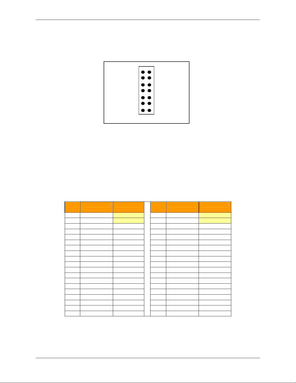
3.4.1 Debug Connector Pinouts
The EVB is fitted with 14-pin JTAG / ONCE and 38-pin Nexus debug connectors. The following diagram
shows the 14-pin JTAG / ONCE connector pinout (0.1” keyed header).
TDI 1
TDO3
TCLK 5
5v EVTI 7
RESET 9
VDDE2 11
RDY 13
Figure 3-8. MPC5668 JTAG / ONCE Connector
The Nexus module used on the MPC5668 family uses the JTAG pins (for control of the Nexus block) along
with additional Nexus pins for trace messages. Nexus mode is entered by a JTAG sequence whereby the
Nexus EVTI pin is sampled on the rising edge of the JTAG TRST pin. If the EVTI is asserted on TRST, Nexus
is enabled.
The table below shows the pinout of the 38-pin MICTOR Nexus connector for the MPC5668
Table 3-13. NEXUS Debug Connector Pinout
2 VSS
4 VSS
6 VSS
8 N/C
10 TMS
12 VSS
14 JCOMP
No
No
1 Reserved --- 2 Reserved --3 Reserved --- 4 Reserved --5 MDO[9] MCU M5 6 CLKOUT MCU PK9
7 Vendor I/O-2 TP25 8 MDO[8] MCU L5
9 Reset-In Reset CCT 10 EVTI MCU M11
11 TDO MCU M3 12 VREF 3.3V Reg
13 MDO[10] MCU M6 14 RDY TP29
15 TCLK MCU P3 16 MDO[7] MCU K5
17 TMS MCU L3 18 MDO[6] MCU J5
19 TDI MCU J3 20 MDO[5] MCU J6
21 TRST JCOMP 22 MDO[4] MCU H6
23 MDO[11] MCU M7 24 MDO[3] MCU H5
25 Tool I/O-3 TP26 26 MDO[2] MCU G5
27 Tool I/O-2 TP27 28 MDO[1] MCU F5
29 Tool I/O-1 TP28 30 MDO[0] MCU E5
31 UBATT 12V Vin 32 EVTO MCU M12
33 UBATT 12V Vin 34 MCK0 MCU M10
35 Tool I/O-0 TP30 36 MSE1 MCU M9
37 VALTREF 3.3V Reg 38 MSEO MCU M8
Note - In order to preserve the ability to accurately measure power consumption on the MCU pins, the JTAG
and Nexus connector reference voltages will be sourced directly from the 5V regulator or from the 12V
unregulated input.
MPC5668EVBUM/D Page 14 of 29
Page 19
MPC5668EVB Users Manual Rev 0.1 May 2009
Jumper
Position
PCB Legend
Description
(D)
(D)
REMOVED
No
12v
power is applied to CAN transceivers
(D)
(D)
(D)
REMOVED
MCU CNTX
-B
is NOT routed to CAN controller
.
(D)
(D)
(D)
(D)
3.5 CAN Configuration (J20, J21, J29, J30, J31)
The CAN section is located
in the top right corner of the
EVB in an area marked
“CAN”
The EVB has 2x NXP TJA1041T high speed CAN transceiver on the MCU CAN-A and CAN-B channels.
These can operate with 5v or 3.3v I/O from the MCU. This is determined by VDDE2 domain. For flexibility, the
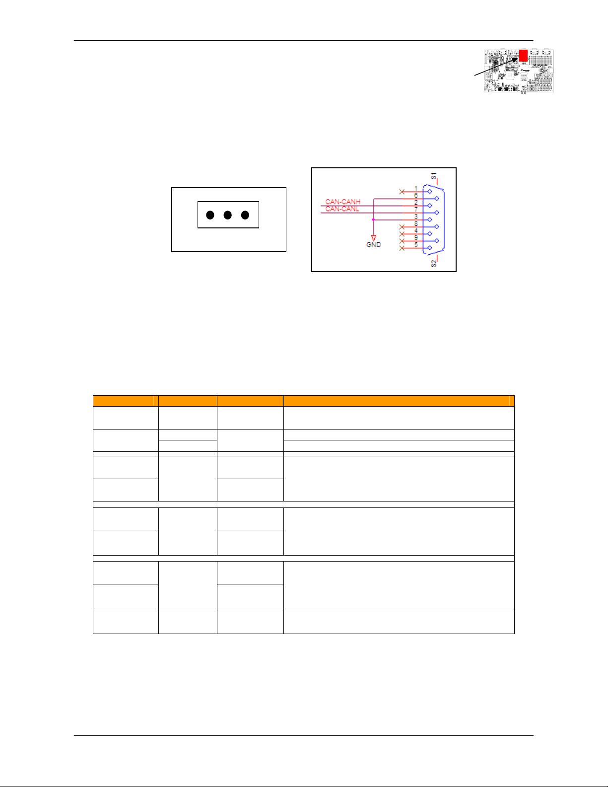
CAN transceiver I/O is connected to a standard 0.1” connector and DB9 connector at the top edge of the
PCB. Connectors P11 and P3A provides the CAN bus level signal interface for CAN-A and connector P10 and
P3B for CAN-B. The pinout for these connectors is shown below.
1
HI LOW
GND
Figure 3-9 CAN Physical Interface Connector
Each of the MCU signals to the CAN transceivers is jumpered, allowing the transceiver to be isolated if that
MCU pin is not configured or used for CAN operation. There is a 2x2 jumper for each CAN channel (one for
Rx, one for Tx). There are also two power jumpers (J30) to physically remove power (12v and 5v) from both of
the CAN transceivers. Jumpers J20 (CAN B) and J21 (CAN A) are configuration jumpers for each of the
Transceivers to control Wake, Standby and Enable. Jumpers can be fitted to select default values or wires
can be used to connect these pins to the MCU.
Table 3-14 CAN Control Jumpers (J30, J31, J7)
J30
Posn 1-2
J30
Posn 3-4
J31 (CAN-A)
Posn 1-2
J31 (CAN-A)
Posn 3-4
J29 (CAN-B)
FITTED
REMOVED
FITTED
FITTED
REMOVED
FITTED
REMOVED
FITTED
Posn 1-2
J29 (CAN-B)
Posn 3-4
J20 & J21
Posn 1-2
J20 & J21
Posn 3-4
J20 & J21
Posn 3-4
FITTED
REMOVED
FITTED
REMOVED
FITTED
REMOVED
FITTED
REMOVED
TX
RX
TX
RX
WAKE
STB
EN
5v is applied to both CAN transceivers VCC
No 5v power is applied to CAN transceivers
12v Power is applied to both CAN transceivers VBAT
MCU CNTX-A is connected to CAN controller A
MCU CNTX-A is NOT routed to CAN controller.
MCU CNRX-A is connected to CAN controller A
MCU CNRX-A is NOT routed to CAN controller.
MCU CNTX-B is connected to CAN controller C
MCU CNRX-B is connected to CAN controller C
MCU CNRX-B is NOT routed to CAN controller.
CAN Transceiver WAKE is connected to GND
WAKE is not connected and available on Pin 2
CAN Transceiver STB is connected to 5v
STB is not connected and available on Pin 4
CAN Transceiver is Enabled
EN is not connected and available on Pin 6
Access to the Error and inhibit signals from the transceivers is provided on J33 and J34.
The prototyping area provides features that allow for additional CAN interfaces to be added to the EVB.
Please see Section 6.2 for details.
Notes
- Care should be taken when fitting the jumper headers as they can easily be fitted in the incorrect
orientation.
MPC5668EVBUM/D Page 15 of 29
Page 20
MPC5668EVB Users Manual Rev 0.1 May 2009
Jump
er Position
PCB Legend
Description
(D)
(D)
(D)
(D)
(D)
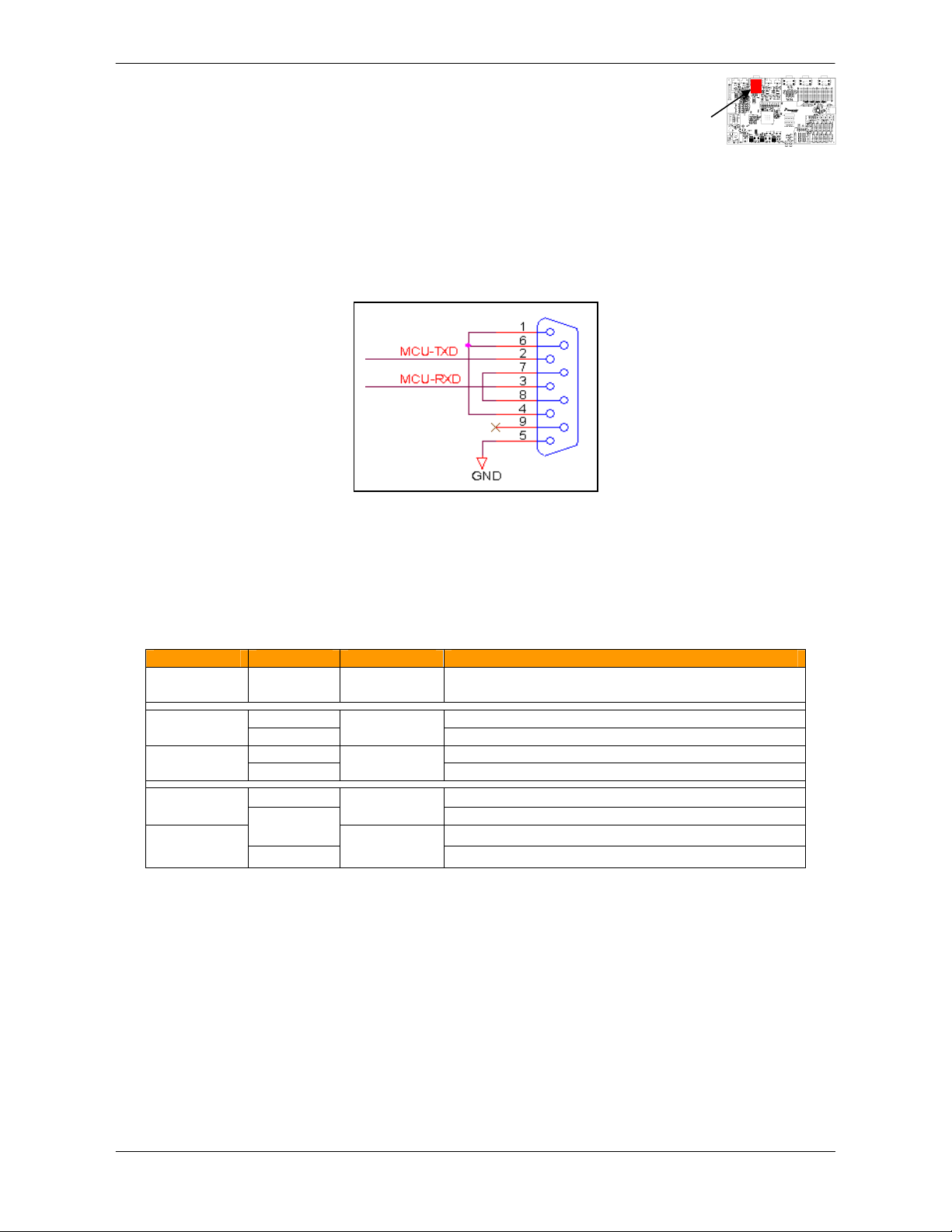
3.6 RS232 Configuration (J6, J17, J18, J23, J24)
The RS232 circuitry
is located at the top
edge of the EVB in
an area titled “SCI”
The EVB has a single MAX3223 RS232 transceiver device, providing RS232 signal translation for the MCU
SCI channels A and B.
Each of the two RS232 outputs from the MAX232 device is connected to a DB9 connector, allowing a direct
RS232 connection to a PC or terminal. Connector P1A provides the RS232 level interface for MCU SCI-A and
P1B for MCU SCI-B. The pinout of these connectors is detailed below. Note that hardware flow control is not
supported on this implementation.
Figure 3-10 RS232 Physical Interface Connector
The MPC5668 eSCI also provides hardware LIN master capability which is supported on the EVB via LIN
transceivers. Jumpers J17, J18, J23 and J24 are provided to isolate the MCU SCI signals from the RS232
interface as described below. There is also a global power jumper (J9) controlling the power to the RS232
transceiver.
Table 3-15 RS232 Control Jumpers
J6
(SCI-PWR)
J18 (SCI-A)
J17 (SCI-A)
J23 (SCI-B)
J24 (SCI-B)
FITTED
REMOVED
FITTED
REMOVED MCU TXD-A signal is disconnected from CAN/LIN
FITTED
REMOVED MCU RXD-A signal is disconnected from CAN/LIN
FITTED
REMOVED MCU TXD-B signal is disconnected from CAN/LIN
TXD
RXD
TXD
FITTED
REMOVED MCU RXD-B signal is disconnected from CAN/LIN
RXD
Power is applied to the MAX3223 transceiver
No power is applied to the MAX3223 transceiver
MCU TXD-A is routed to MAX3223
MCU RXD-A is routed via MAX3223
MCU TXD-B is routed via MAX3223
MCU RXD-B is routed via MAX3223
The default configuration enables SCI-A and SCI-B channels. RS232 compliant interfaces (with no hardware
flow control) are available at DB9 connector P1. If the MCU is configured such that SCI-A or SCI-B is set as a
normal I/O port, then the relevant jumpers must be removed to avoid any conflicts occurring. If required,
jumper J6 can be used to completely disable the SCI transceiver.
MPC5668EVBUM/D Page 16 of 29
Page 21
MPC5668EVB Users Manual Rev 0.1 May 2009
Jumper
Position
PCB Legend
Description
(D)
(D)
(D)
(D)
(D)
(D)
(D)
(D)
LIN
3.7 LIN Configuration (J3, J4, J5, J12,
J13, J14, J15,J16)
The LIN circuitry is
located in the top edge
of the EVB in an area
titled “LIN”
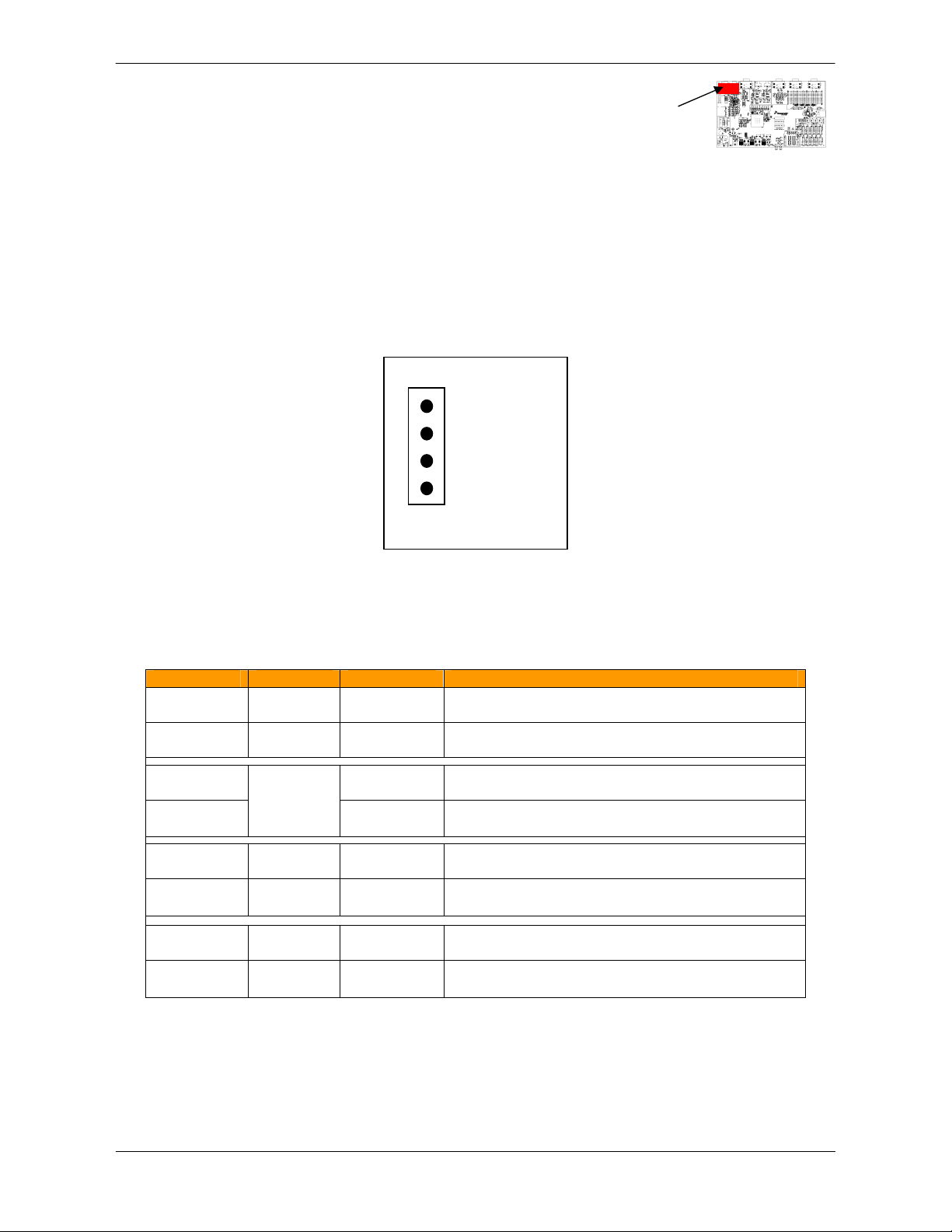
The EVB is fitted with two Freescale MCZ33661EF LIN transceivers. The eSCI module incorporates a
hardware controlled LIN master, and as such, the LIN transceivers are connected to the TX and RX signals of
SCI C and D.
For flexibility, the LIN transceivers are connected to a standard 0.1” connector (P7 for LIN-C and P6 for LIN-D)
and a 4 pin molex connector (J2 for LIN-C and J1 for LIN-D) at the top edge of the PCB as shown in the figure
below. For ease of use, the 12V EVB supply is fed to pin1 of the connectors and the LIN transceiver power
input to pin 2. This allows the LIN transceiver to be powered directly from the EVB supply by simply linking
pins 1 and 2 of connector P7/P6 using a 0.1” jumper shunt.
P7/P8
1
VDD UNREG
LIN VSUP
LIN
GND
Figure 3-11 LIN Physical Interface Connectors
Along with the MCU signal routing jumpers (J10 / J11), there is are jumpers (J5 / J6) to enable or disable the
LIN transceiver and jumpers (J1 and J2) which determines if the LIN transceiver is operating in master or
slave mode, as defined in the table below.
Table 3-16 LIN Control Jumpers
J5
(LIN C-M)
J3
(LIN D-M)
J16*
(LIN C-EN)
J12*
(LIN D-EN)
J14 (SCI-C)
J15 (SCI-C)
J14 (SCI-D)
J15 (SCI-D)
FITTED
REMOVED
FITTED
REMOVED
FITTED
REMOVED
FITTED
REMOVED
FITTED
REMOVED MCU TXD-C signal is disconnected LIN Physical
FITTED
REMOVED MCU RXD-C signal is disconnected LIN Physical
FITTED
REMOVED MCU TXD-D signal is disconnected LIN Physical
FITTED
REMOVED MCU RXD-D signal is disconnected LIN Physical
TXD
RXD
TXD
RXD
LIN-C transceiver is configured for LIN Master mode
LIN-C transceiver is configured for LIN Slave mode
LIN-D transceiver is configured for LIN Master mode
LIN-D transceiver is configured for LIN Slave mode
The LIN-C transceiver is enabled
The LIN-C transceiver is disabled
The LIN-D transceiver is enabled
The LIN-D transceiver is disabled
MCU TXD-C is routed to LIN Physical
MCU RXD-C is routed to LIN Physical
MCU TXD-D is routed to LIN Physical
MCU RXD-D is routed to LIN Physical
* Note – Jumpers J3/J5 do NOT route power to LIN transceivers, they only control an enable line on the LIN
device. Power to the LIN transceiver is supplied via connectors P7 / P8, Pin 2.
The Default LIN configuration is with the module enabled in master mode, LIN slave mode can be enabled by
removing jumpers J3 / J5.
MPC5668EVBUM/D Page 17 of 29
Page 22
MPC5668EVB Users Manual Rev 0.1 May 2009
Jumper
Position
PCB
Descrip
tion
(D)
(D)
(D)
(D)
(D)
(D)
Jumper
Position
PCB
Description
(D)
(D)
(D)
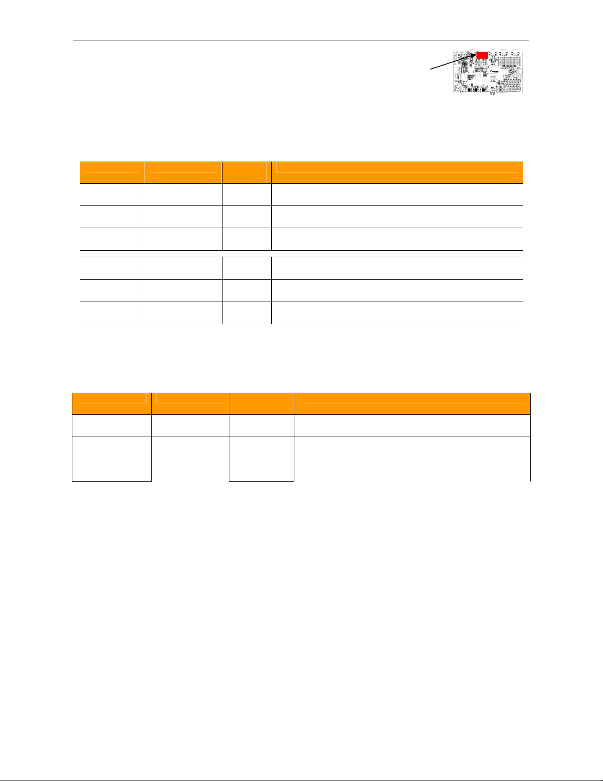
3.8 FlexRAY Configuration
(J19, J27, J25, J26, J28)
The Flexray circuitry is
located in the top edge of
the EVB in an area titled
“Flexray”
The EVB is fitted with 2 FlexRAY physical interfaces connected to MCU FlexRAY channels A and B. Jumpers
J19 and J27 are provided to route the respective MCU signals to the physical interfaces as described below.
Table 3-17 Flexray MCU Signal Routing Jumpers (J19, J27)
Legend
J19 (Flex-A)
Posn 1-2
J19 (Flex-A)
Posn 3-4
J19 (Flex-A)
Posn 5-6
FITTED
REMOVED MCU PK4 is not connected to Flexray A transceiver TX
FITTED
REMOVED MCU PK5 is not connected to Flexray A transceiver TXEN
FITTED
REMOVED MCU PK3 is not connected to Flexray A transceiver RXEN
TX
TXEN
RX
MCU PK4 is connected to Flexray A transceiver TX
MCU PK5 is connected to Flexray A transceiver TXEN
MCU PK3 is connected to Flexray A transceiver RX
J27 (Flex-B)
Posn 1-2
J27 (Flex-B)
Posn 3-4
J27(Flex-B)
Posn 5-6
FITTED
REMOVED MCU PK7 is not connected to Flexray B transceiver TX
FITTED
REMOVED MCU PK8 is not connected to Flexray B transceiver TXEN
FITTED
REMOVED MCU PK6 is not connected to Flexray B transceiver RXEN
TX
TXEN
RX
MCU PK7 is connected to Flexray B transceiver TX
MCU PK8 is connected to Flexray B transceiver TXEN
MCU PK6 is connected to Flexray B transceiver RX
The power to the Flexray physical interface is controlled via jumper J25 to allow disconnection if required. The
Flexray physical interface is capable of interfacing with MCU I/O voltages of 3.3V or 5.0V as defined by the
voltage supplied VDDE2 via jumper J42.
Table 3-18 Flexray Power Control Jumpers (J25)
Legend
J25 (Flex-PWR)
Posn 1-2
J25 (Flex-PWR)
Posn 3-4
J25 (Flex-PWR)
Posn 5-6
FITTED
REMOVED 12V Flexray circuitry is not powered
FITTED
REMOVED 5V Flexray circuitry is not powered
FITTED
REMOVED VIO Flexray circuitry is not powered
12V
5V
VIO
12V Flexray circuitry is powered from main 12V input
5V Flexray circuitry is powered from 5.0V switching reg
VIO Flexray circuitry is powered from VDDE2
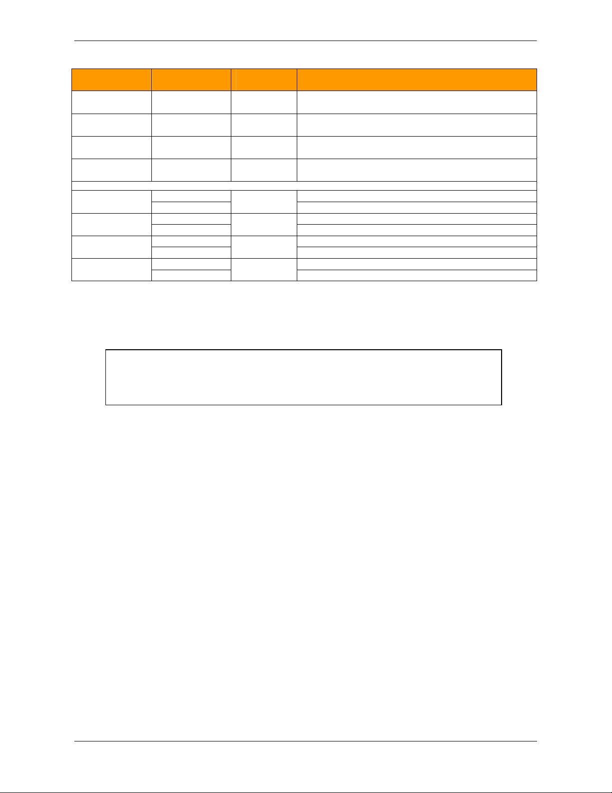
The flexray interface has 4 pins which are used for configuration and are pulled high or low controlled by a
jumper as described in the table below. By default, all of the jumper headers are fitted. Please consult the
Flexray physical interface specification before changing any of these jumpers.
MPC5668EVBUM/D Page 18 of 29
Page 23
MPC5668EVB Users Manual Rev 0.1 May 2009
Jumper
Position
PCB
Description
(D)
(D)
(D)
(D)
J28 (Flex
-B)
(D)
J28 (Flex
-B)
(D)
J28 (Flex
-B)
(D)
J28 (Flex
-B)
(D)
Important:
Table 3-19 Flexray Control Jumpers (J26, J28)
Legend
J26 (Flex-A)
Posn 1-2
J26 (Flex-A)
Posn 3-4
J26 (Flex-A)
Posn 5-6
J26 (Flex-A)
Posn 7-8
FITTED
REMOVED Flexray-A interface BGE signal is unterminated
FITTED
REMOVED Flexray-A interface EN signal is unterminated
FITTED
REMOVED Flexray-A interface STBN signal is unterminated
FITTED
REMOVED Flexray-A interface WAKE signal is unterminated
BGE
EN
STBEN
WAKE
Flexray-A interface BGE signal is pulled to VIO
Flexray-A interface EN signal is pulled to VIO
Flexray-A interface STBN signal is pulled to VIO
Flexray-A interface WAKE signal is pulled to GND
Posn 1-2
Posn 3-4
Posn 5-6
Posn 7-8
FITTED
REMOVED Flexray-B interface BGE signal is unterminated
FITTED
REMOVED Flexray-B interface EN signal is unterminated
FITTED
REMOVED Flexray-B interface STBN signal is unterminated
FITTED
REMOVED Flexray-B interface WAKE signal is unterminated
BGE
EN
STBEN
WAKE
Flexray-B interface BGE signal is pulled to VIO
Flexray-B interface EN signal is pulled to VIO
Flexray-B interface STBN signal is pulled to VIO
Flexray-B interface WAKE signal is pulled to GND
Notes:
- The flexray physical interfaces are connected to 2 pin molex connectors (FlexRAY A) 1.25mm
shrouded 2-pin connectors to connect to the flexray bus (as are standard fit on many Freescale
development platforms using flexray).
A 40Mhz oscillator is required for the correct operation of the flexray controller. Please
ensure that the 40Mhz crystal is selected as the system clock or use a 40Mhz external
clock source.
MPC5668EVBUM/D Page 19 of 29
Page 24
MPC5668EVB Users Manual Rev 0.1 May 2009
PG[9]
PG[7]
PG[12]
Down (GND)
2.2kΩ
PG
[13]
PG[14]
PG[15]
PH[1]
PH[2]
PH[3]
Down (GND)
2.2kΩ
PH[4]
PH[5]
PH[6]
PH[7]
Jumper
Position
PCB
Description
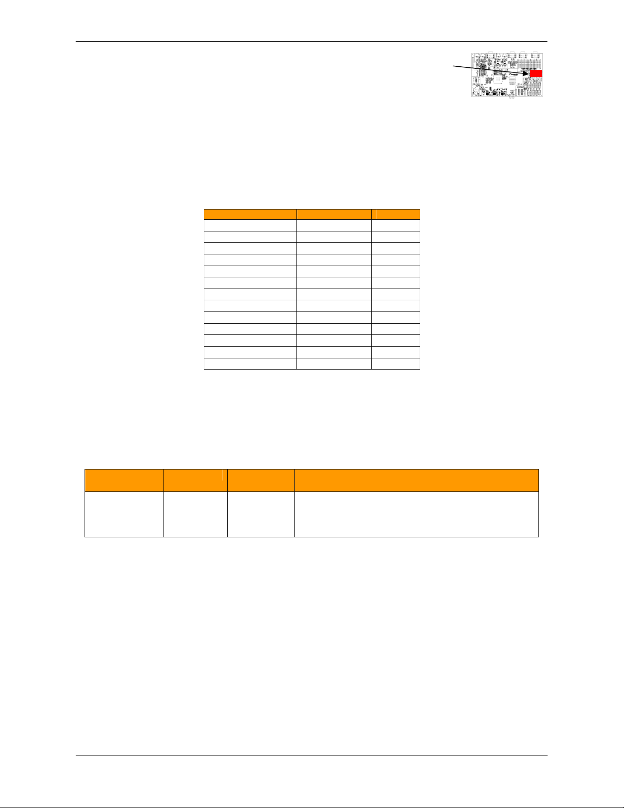
3.9 Ethernet
The Ethernet circuitry is
located in the right edge of
the EVB in an area titled
“Ethernet”
The EVB is fitted with a National Semiconductor DP8348C Ethernet physical interface (U9) and a Pulse Jack
J1011F21PNL RJ45 connector with integrated activity LED’s and magnetics (J63).
The National Semiconductor DP8348C physical interface is connected to the MII on the MPC5668. This is a
fixed connection with no means of isolation. Pullups are also also present on some of these signals. These
are detailed in the table below. Please be aware of this when using I/O on ports G and H.
Table 3-20 Pull up/ Pull down resistors on Ports G and H for Ethernet Physical
Port Pin Pull Direction Strength
Down (GND) 2.2kΩ
Up (3.3v SR) 1.5kΩ
Down (GND) 2.2kΩ
Down (GND) 2.2kΩ
Down (GND) 2.2kΩ
Down (GND) 2.2kΩ
Down (GND) 2.2kΩ
Down (GND) 2.2kΩ
Down (GND) 2.2kΩ
Down (GND) 2.2kΩ
Down (GND) 2.2kΩ
The VDDE3 voltage domain that is used by ports G and H should be set to 3.3v (J44 Pos 2-3) when power is
applied to the physical interface.
Power can be removed from the physical interface via J62.
Table 3-21 Ehternet Physical Interface Power Supply Enabled (J26)
Legend
J62
(PHY PWR)
FITTED (D)
PHY PWR
REMOVED
The DP4348C Ethernet Physical Interface is powered
from the 3.3v SR.
The DP4348C Ethernet Physical Interface is not
powered
MPC5668EVBUM/D Page 20 of 29
Page 25
MPC5668EVB Users Manual Rev 0.1 May 2009
left
Jumper
Position
PCB Legend
Description
(D)
(D)
(D)
MLBDI
9
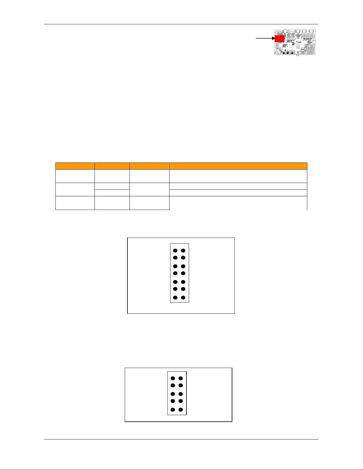
3.10 MLB and Most
The MLB and MOST
circuitry is located on the
edge of the EVB .
The EVB is fitted with a range of hardware to support the MOST communication protocol. These include:
SMSC OS81050 (U6) INIC interfaced to the MPC5668 via 3 pin Media Local Bus (MLB) interface.
INIC JTAG port (P12) and MLB monitor port (J88)
Tyco Physical optical transceiver (U8) interfaced to the SMSC OS81050
Dual footprint layout to allow the SMSC OS81050 to be replaced with the smaller ROM alternative
40 Pin header to allow the EVB to be interfaced to the MOST 150 EVB from SMSC.
Power Jumpers on the EVB are configured to allow the EVB to supply power to both the ROM and Flash
versions of the SMSC OS81050 INIC that are supported by the dual footprint on the EVB. By default the Flash
version of the OS81050 is fitted to the EVB. The jumpers also allow power to be removed from the INIC. The
power supply jumpers are detailed below. All Power supplies domains referred to in this table are for the Flash
based INIC. Please refer to the schematics to see how this affects the supply domains of the ROM INIC if it
has been fitted.
Table 3-22 INIC Power Supply Control (J35, J36, J55)
J35
J36
J55
FITTED
REMOVED
FITTED
REMOVED
FITTED
REMOVED
3.3v PWR
2.5v PWR
2.5v PWR
3.3v is applied to VDDP1 and VDDP2 of the INIC
No 3.3v power is applied to VDDP1 and VDDP2
2.5v is applied to VDDA1 and VDDA2.
No power is applied to VDDA1 and VDDA2.
2.5v is applied to VDDC1 and VDDC2.
No power is applied to VDDC1 and VDDC2.
The Pin out for the INIC JTAG connector filled to the EVB is show in Figure x below:
N/C 1
N/C 3
VSS 5
TDI 7
3.3v 9
TDO 11
N/C 13
2 VSS
4 INIC /BOOT
6 3.3v
8 TCK
10 VSS
12 RST
14 TMS
Figure 3-12. INC5668 JTAG Connector
The INIC pins MLBDI, MLBSI, RMCK, SCK and FSY are brought out to the header J22, to allow for monitoring
and control if required. J88 provides the MLB monitor header that is compatible with the SMSC MLB Monitor
hardware. The Pin out of this is shown in Figure x below.
MLBCLK 1
MLBSIG 3
MLBDAT 5
MLBSI 7
2 VSS
4 VSS
6 VSS
8 VSS
10 VSS
Figure 3-13. MLB Monitor Connector
MPC5668EVBUM/D Page 21 of 29
Page 26
MPC5668EVB Users Manual Rev 0.1 May 2009
Jumper
Position
PCB Legend
Description
(D)
(D)
(D)
(D)
EVB SDA is Routed to the EVB INIC
(D)
(D)
(D)
EVB SCL is Rout
ed to the EVB INIC
(D)
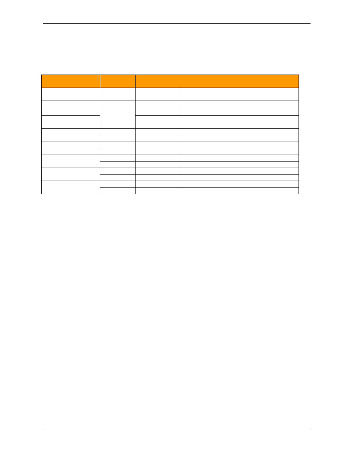
Port J11 is placed on the edge of the EVB to allow the SMSC MOST 150 EVB to be interfaced to the
MPC5668EVB. This allows for evaluation of the MOST150 INIC with the MPC5668. To use this connector the
signals must be routed from the on chip INIC to this connector using the Jumpers detailed in table x below.
Removing these Jumpers also allow the signals between the INIC and the MCU to be isolated.
J37(MLBCLK)
J38(PSO)
J39(MLBDAT)
J40(SDA)
J57(PS1)
J58 (/INT)
J59 (SCL)
J65 (MLBSIG)
Table 3-23 INIC Signal Control
1-2
EVB MLBCLK is Routed to the EVB INIC
2-3 INIC150 MLBCLK is Routed to the MOST150 header
1-2
2-3
1-2
EVB
INIC150
EVB MLBDAT is Routed to the EVB INIC
PSO is Routed to the EVB INIC
PSO is Routed to the MOST150 header
2-3 INIC150 MLBDAT is Routed to the MOST150 header
1-2
2-3 INIC150 SDA is Routed to the MOST150 header
1-2
EVB PS1 is Routed to the EVB INIC
2-3 INIC150 PS1 is Routed to the MOST150 header
1-2
EVB /INT is Routed to the EVB INIC
2-3 INIC150 /INT is Routed to the MOST150 header
1-2
2-3 INIC150 SCL is Routed to the MOST150 header
1-2
EVB MLBSIG is Routed to the EVB INIC
2-3 INIC150 MLBSIG is Routed to the MOST150 header
The status and reset lines can also be isolated via J56 and J64.
If required the standard fit INIC can be removed and replaced with the ROM memory alternate. Please
observe the power supply requirements of the device.
MPC5668EVBUM/D Page 22 of 29
Page 27
MPC5668EVB Users Manual Rev 0.1 May 2009
Jumper
Position
PCB Legend
Description
(D)
(D)
(D)
(D)
(D)
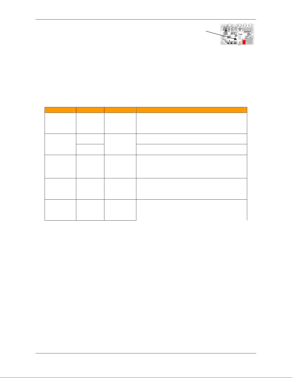
3.11 Phantom Ports (J76, J77,
J78, J79, J80)
The Phantom port
circuitry is located on the
bottom edge of the EVB
To support the de-serialisation feature of the MPC5668 DSPI module, the EVB features 4 chained SIPO shift
registers interfaced to DSPI A. This allows a 32-bit phantom port to be created. The port can operate at either
5V or 3.3V depending on the VDDE2 supply voltage (J42). This is outputted on P24 and P25. Please refer to
the MPC5668 Reference manual for guideline on how to create software to interface to the phantom part.
Five jumpers are used to allow the signals and power to be isolated from the phantom port circuitry. These are
detailed in table x below.
Table 3-24 Phantom Port Control (J35, J36, J55)
J76
FITTED
REMOVED
CLK
PF0 DSPI A CLK is connected to the phantom port
circuitry.
PF0 DSPI A CLK is disconnected from the phantom
port circuitry.
J77
FITTED
REMOVED
SREG PWR
VDDE2 Domain power is applied to the 4 shift
registers (U15, U16, U21, U22)
No power is applied to the 4 shift registers (U15,
U16, U21, U22)
FITTED
PF1
DSPI_A Serial Data Out
is connected to the
phantom port circuitry.
J78
REMOVED
IN
PF1
DSPI_A Serial Data Out
is disconnected from the
phantom port circuitry.
J79
FITTED
REMOVED
CLR
PF11 is connected to the phantom port circuitry.
Allows for software to reset the Shift registers.
PF11 is disconnected from the phantom port
circuitry.
J80
FITTED
REMOVED
OUT
PF3 DSPI A PCS is connected to the phantom port
circuitry.
PF3 DSPI A PCS is disconnected from the phantom
port circuitry.
MPC5668EVBUM/D Page 23 of 29
Page 28
MPC5668EVB Users Manual Rev 0.1 May 2009
CANA
CANB
SCIA
PD[12,13]
SCIB
PD[
14,15]
LINC
LIND
FlexRay A
FlexRay B
Reset
Ethernet
PG[12..15
]
P
H[3..7
]
MOST
/MLB
User RVAR
Phantom
4. MCU Pin Usage Map
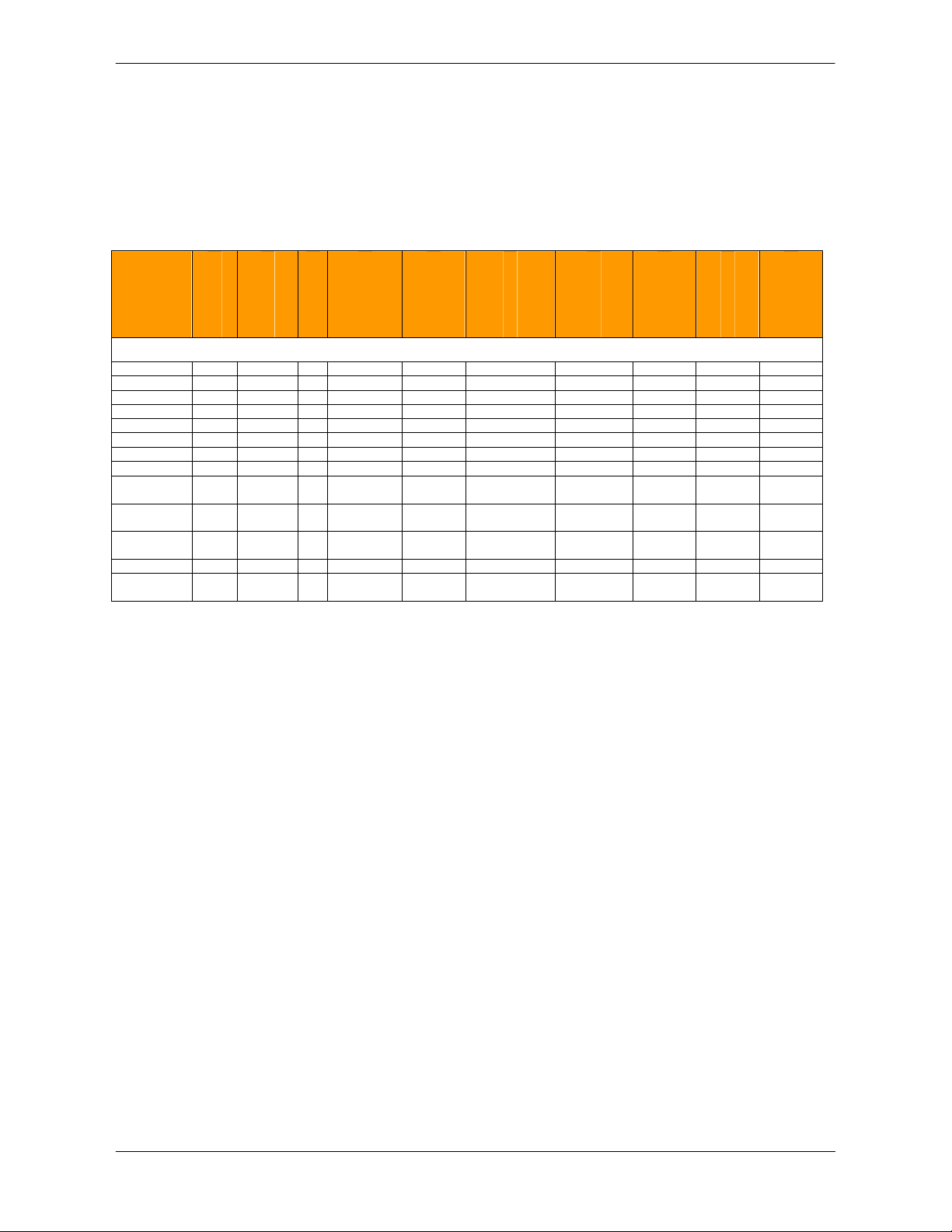
The table below provides a useful cross reference to see what MCU port pins are used by the various EVB
peripherals and functions. Note that there are some overlapping functions for example the Nexus and External
bus as shown by the shaded boxes in the table below.
Table 4-1. EVB MCU Pin Usage
Port A
Function
Port B
Port C
Port D
Port E
Port F
Port G
Port H
Port J
Port k
Enabled By Default
PD[0..1]
PD[2..3]
PE[0,1]
PE[2,3]
PK[3..5]
PK[6..8]
PK[9]
Config
PG[6..9]
PB[0,1] PG[0]
PA[0]
PF[0,1,3, 11]
Port
PG[2..5]
PH[0,1]
PK[0..2]
MPC5668EVBUM/D Page 24 of 29
Page 29

MPC5668EVB Users Manual Rev 0.1 May 2009
J1
J2
J3 (LIN
-D)
J4 (
LIN D
)
J5 (LIN
C)
J6 (SCI
-
PWR)
J7 (FlexRAY)
J8 (FlexRAY)
J9 (FlexRAY)
J10 (FlexRAY)
J11
J12 (LIN
-D)
J13 (LIN D
)
J14 (LIN C
)
J15 (LIN C)
J16 (LIN C
)
J17 (SCI A)
J18 (SCI A)
J19
(Flex
-A)
J19 (Flex
-A)
J19 (Flex
-A)
J20 (CAN A)
J20 (CAN A)
J20 (CAN A)
J21 (CAN B)
J21 (CAN B)
J21 (CAN B)
J22
J23 (SCI-B)
J24 (SCI-B)
J25 (Flex
-
PWR)
J25 (Flex
-
PWR)
J25
(Flex
-
PWR)
5. Default Jumper Summary Table
The following table details the DEFAULT jumper configuration of the EVB as explained in detail in section 3.
Table 5-1 Default Jumper Positions
Jumper Default
Posn
LIN MOLEX – No Jumpers
PCB
Legend
Description
LIN MOLEX – No Jumpers
FITTED MASTER LIN D Bus Master Mode Enabled
FITTED LIN D RX LIN D RX from MCU Connected to LIN Interface
FITTED MASTER LIN C Bus Master Mode Enabled
FITTED Power is applied to the SCI transceiver
FITTED CAP A DIS FlexRAY Decoupling CAP Disable
FITTED CAP A DIS FlexRAY Decoupling CAP Disable
FITTED CAP B DIS FlexRAY Decoupling CAP Disable
FITTED CAP B DIS FlexRAY Decoupling CAP Disable
External Port No Jumpers
FITTED LIN D EN LIN D Bus Enable Physical Interface
FITTED LIN D TX LIN D TX from MCU Connected to LIN Interface
FITTED LIN C TX LIN C TX from MCU Connected to LIN Interface
FITTED LIN C RX LIN C RX from MCU Connected to LIN Interface
FITTED LIN C EN LIN D Bus Enable Physical Interface
FITTED SCI A RX MCU RXD-A is routed to MAX3223
FITTED SCI A TX MCU TXD-A is routed to MAX3223
Posn 1-2
Posn 3-4
Posn 5-6
Posn 1-2
Posn 3-4
Posn 3-4
Posn 1-2
Posn 3-4
Posn 3-4
FITTED TX MCU PK4 is connected to FlexRay A transceiver TX
FITTED TXEN MCU PK5 is connected to FlexRay A transceiver TXEN
FITTED RX MCU PK3 is connected to Flexray A transceiver RXEN
FITTED WAKE CAN Transceiver WAKE is connected to GND
FITTED STB CAN Transceiver STB is connected to 5v
FITTED EN CAN Transceiver is Enabled
FITTED WAKE CAN Transceiver WAKE is connected to GND
FITTED STB CAN Transceiver STB is connected to 5v
FITTED EN CAN Transceiver is Enabled
MLB Monitor No Jumpers
FITTED TXD MCU TXD-B is routed via MAX3223
FITTED RXD MCU RXD-B is routed via MAX3223
Posn 1-2
Posn 3-4
Posn 5-6
FITTED 12V 12V Flexray circuitry is powered from main 12V input
FITTED 5V 5V Flexray circuitry is powered from 5.0V switching reg
FITTED VIO VIO Flexray circuitry is powered from VDDE2
MPC5668EVBUM/D Page 25 of 29
Page 30

MPC5668EVB Users Manual Rev 0.1 May 2009
J26
(Flex
-A)
J26 (Flex
-A)
J26 (Flex
-A)
J26 (Flex
-A)
J27 (Flex
-B)
J27 (Flex
-B)
J27(Flex
-B)
J28 (Flex
-B)
J28 (Flex
-B)
J28 (Flex
-B)
J28 (Flex
-B)
J29 (CAN
-B)
J
29 (CAN
-B)
J30 (CAN)
J30 (CAN)
J31
(CAN
-
A)
J31
(CAN
-
A)
J33
J34
J35
J36
J37(
MLBCLK
)
J38(PSO
)
J39(MLBDAT)
J
40(SDA)
1-2 EVB SDA is Routed to the EVB INIC
J
41
(VDDE
4)
J
42
(VDDE
2)
J
43
(VDDE
1)
J
44
(VDDE
3)
J
45 (VDDEMLB)
J46 (VRC)
1-2 5V VRC is
supplied from
the
5V switching regulator
J47
(VRCSEL
)
J48
(VDD33)
J49
(VDDA)
J50
(VDDSYN)
Jumper Default
Posn 1-2
Posn 3-4
Posn 5-6
Posn 7-8
Posn 1-2
Posn 3-4
Posn 5-6
Posn 1-2
Posn 3-4
Posn 5-6
Posn 7-8
Posn 1-2
Posn 3-4
Posn 1-2
Posn 3-4
Posn 1-2
Posn 3-4
J32 (JRST)
Posn
FITTED BGE
FITTED EN
FITTED STBEN
FITTED WAKE
FITTED TX
FITTED TXEN
FITTED RX
FITTED BGE
FITTED EN
FITTED STBEN
FITTED WAKE
FITTED TX
FITTED RX
FITTED VCC
FITTED VIO
FITTED TX
FITTED RX
1-2
PCB
Legend
BUF
Description
Flexray-A interface BGE signal is pulled to VIO
Flexray-A interface EN signal is pulled to VIO
Flexray-A interface STBN signal is pulled to VIO
Flexray-A interface WAKE signal is pulled to GND
MCU PK7 is connected to Flexray B transceiver TX
MCU PK8 is connected to Flexray B transceiver TXEN
MCU PK6 is connected to Flexray B transceiver RX
Flexray-B interface BGE signal is pulled to VIO
Flexray-B interface EN signal is pulled to VIO
Flexray-B interface STBN signal is pulled to VIO
Flexray-B interface WAKE signal is pulled to GND
MCU CNTX-B is connected to CAN controller C
MCU CNRX-B is connected to CAN controller C
5v is applied to both CAN transceivers VCC
Power is applied to both CAN transceivers VIO
MCU CNTX-A is connected to CAN controller A
MCU CNRX-A is connected to CAN controller A
JTAG reset signal is buffered to MCU RESET pin
(connected to the MCU Reset-In circuitry)
CAN Status – No Jumpers
CAN Status – No Jumpers
FITTED 3.3v PWR 3.3v is applied to VDDP1 and VDDP2 of the INIC
FITTED 2.5v PWR 2.5v is applied to VDDA1 and VDDA2.
1-2 EVB MLBCLK is Routed to the EVB INIC
1-2 EVB PSO is Routed to the EVB INIC
1-2 EVB MLBDAT is Routed to the EVB INIC
MPC5668EVBUM/D Page 26 of 29
1-2 5.0v MCU VDDE4 is powered from 5v
1-2 5.0v MCU VDDE2 is powered from 5v
1-2 5.0v MCU VDDE1 is powered from 5v
1-2 5.0v MCU VDDE3 is powered from 5v
1-2 2.5V MCU VDD pin is powered from 1.5v switching regulator
1-2 INT 3.3 V internal voltage regulator enabled (5 V mode)
REMOVED MCU VDD33 pin is powered from switching regulator
FITTED MCU VDDA is powered from 5V linear regulator
REMOVED MCU VDDSYN pin is powered from switching regulator
Page 31

MPC5668EVB Users Manual Rev 0.1 May 2009
J51 (CAN
F)
J52 (CAN D)
J53 (CAN E)
J54 (CAN
C)
J55
(INIC
PWR
)
J56 (INIC RST)
J
57(INIC PS1)
J
58 (INIC /INT)
J
59 (INIC SCL)
J
60 (INIC BOOT)
J61 (MCU CLK)
J62 (PHY PWR
)
J63
J
64 (
MOST FOT
)
J
65 (MLBSIG)
J66 (MCU CLK)
J67 (32KHz CLK)
J69 (BOOT CFG)
J
71 (32KHz CLK)
J72
J73 (ADC VSUP)
J74
J
75 (1
-2)
J
75 (3
-4)
J81 (5.0v
-
LINEAR)
J82 (2.5v)
J83 (
3.3v
)
J84 (5.0v)
J85 (U20 PWR)
J87 (OSC SEL)
Jumper Default
Posn
PCB
Legend
Description
REMOVED Do not route CAN F to Prototype Area
REMOVED Do not route CAN D to Prototype Area
REMOVED Do not route CAN E to Prototype Area
REMOVED Do not route CAN C to Prototype Area
FITTED 2.5v PWR 2.5v is applied to VDDC1 and VDDC2.
FITTED RST INIC Reset is connected to PB0
1-2 EVB MLB PS1 is Routed to the EVB INIC
1-2
EVB /INT is Routed to the EVB INIC
1-2 EVB SCL is Routed to the EVB INIC
1-2 EVB INIC Boot pin is pulled up to 2.5v Rail
1-2 Y2 MCU Clock is Y2
FITTED PHY PWR
The DP4348C Ethernet Physical Interface is powered
from the 3.3v SR.
RJ45 No Jumpers
1-2 STATUS MOST FOT is Status is connected to PB1
1-2 EVB MLBSIG is Routed to the EVB INIC
1-2 Y2 MCU Clock is Y2
1-2 Y3 32Khz Crystal (Y2) is connected to MCU
J68 (RST-IN)
J70 (TCLK PULL)
FITTED
1-2 FLASH MCU boots from internal flash
1-2
VDDE2
External reset source (LVI, Debug or Target) will be able
to assert MCU reset
JTAG / NEXUS TCLK signal is pulled to VDDE2 via
10KΩ
1-2 Y3 32Khz Crystal (Y2) is connected to MCU
Not Implemented
REMOVED Output from variable resistor RV1 is applied to MCU
PA0
REMOVED On board Voltage levels not connected to EVB
FITTED Enables 3.3v board level LVI
FITTED Enables 5v board level LVI
J76 FITTED CLK
J77
J78
J79
J80
FITTED
FITTED IN
FITTED CLR
FITTED OUT
SREG
PWR
PF0 DSPI A CLK is connected to the phantom port
circuitry.
VDDE2 Domain power is applied to the 4 shift registers
(U15, U16, U21, U22)
PF1
DSPI_A Serial Data Out
is connected to the phantom
port circuitry.
PF11 is connected to the phantom port circuitry. Allows
for software to reset the Shift registers.
PF3 DSPI A PCS is connected to the phantom port
circuitry.
FITTED DISABLE 5.0v linear regulator output is Enabled
REMOVED DISABLE 2.5v switching regulator output is Enabled
REMOVED DISABLE 3.3v switching regulator output is Enabled
REMOVED DISABLE 5.0v switching regulator output is Enabled
FITTED EVB oscillator module U20 is powered
J86 (RV1)
FITTED
1-2 MOD Daughter card EXT-CLK is routed from U20
Output from variable resistor RV1 is applied to MCU
PA0
MPC5668EVBUM/D Page 27 of 29
Page 32
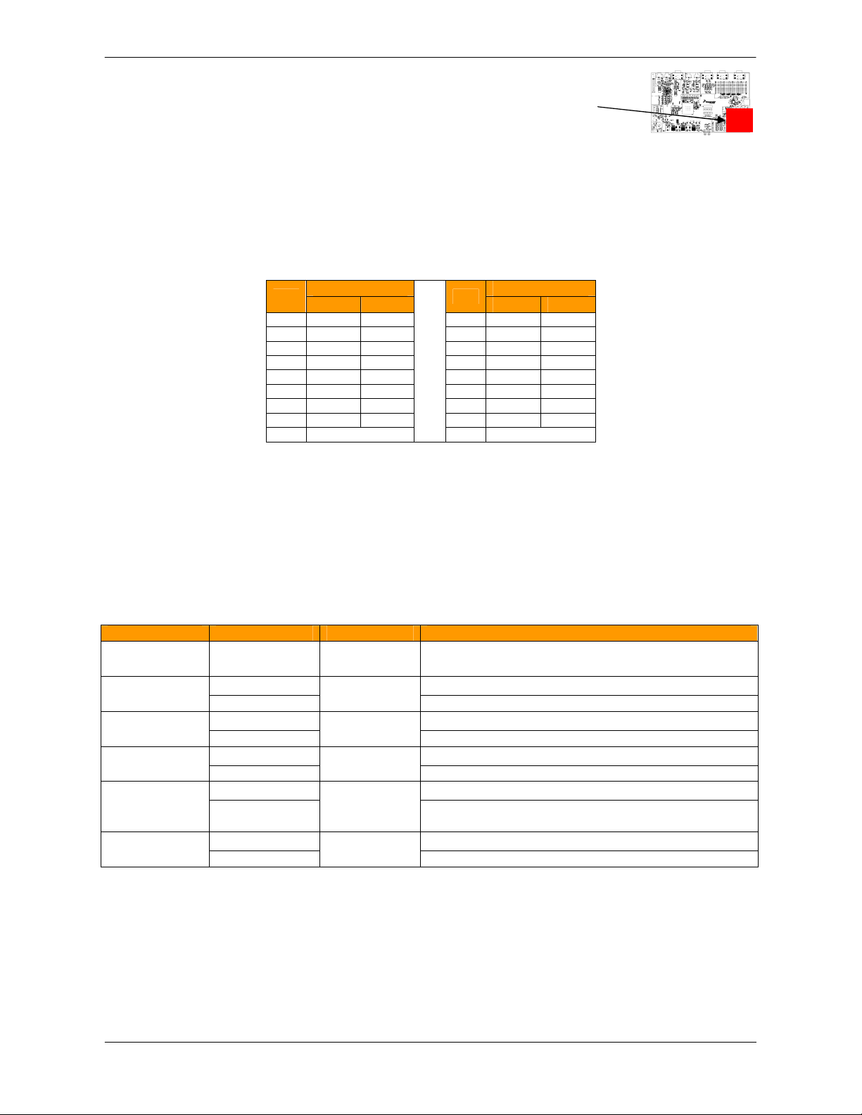
MPC5668EVB Users Manual Rev 0.1 May 2009
Function
Function
GPIO
1st
Alt GPIO
1st
Alt
Jumper
Position
PCB Legen
d Description
J73
J74
J74
J74
J74
The user connectors are
6. User Connector Descriptions
located on the right hand
side of the PCB
This section details the pinout of the EVB user connectors. The connectors are 0.1 inch pitch turned pin
headers and are located to the right hand side of the EVB. Pins are grouped by port functionality and the PCB
legend shows the respective port number adjacent to each pin.
6.1.1 Port A / ADC (Connector J86, RV1, J73 and J74)
Table 6-1. Port A Connector Pinout (P17)
Pin
1 PA0 AN0 2 PA1 AN1
3 PA2 AN2 4 PA3 AN3
5 PA4 AN4 6 PA5 AN5
7 PA6 AN6 8 PA7 AN7
9 PA8 AN8 10 PA9 AN9
11 PA10 AN10 12 PA11 AN11
13 PA12 AN12 14 PA13 AN13
15 PA14 AN14 16 PA15 AN15
17 GND 18 GND
Pin
To provide a quick means of supplying input to the ATD (Analogue To Digital converter), a 2KΩ variable
resistor (RV1) will is connected between P5V and GND, with the output (centre tap) connected to PA0 / AN0
via jumper J86. By removing jumper J86, PA0 is disconnected from the variable resistor and can function as a
normal I/O port. J86 and RV1 are located next to P17.
To allow the EVB core voltages to be monitors by the ATD J74 allows the 2.5v, 3.3v and 5v Switcher and
Linear regulator outputs to be connected to the ATD inputs. J73 allows the 12v EVB supply to be monitored
via resister ladder to reduce the voltage to a level that is in spec of the ATD’s range. 65% of the 12v supply is
applied to the ADC via the resistor ladder.
Table 6-2 RV1 Connection Jumper J8
J86
(RV1)
(ADC VSUP)
POSN 1-2
POSN 3-4
POSN 5-6
POSN 7-8
FITTED
REMOVED (D) Output from RV1 is not connected to MCU (disabled)
FITTED
65% of the output from 12v Reg is applied to PA14
REMOVED (D) 12v Reg Output is not connected to PA14
FITTED
Output from 2.5v Reg is connected to PA10
REMOVED (D) Output from 2.5v Reg is NOT connected to PA10
FITTED
Output from 3.3v Reg is connected to PA10
REMOVED (D) Output from 3.3v Reg is NOT connected to PA10
FITTED
Output from 5v Switching Reg is connected to PA10
REMOVED (D)
FITTED
Output from 5v Linear Reg is connected to PA10
REMOVED (D) Output from 5v Linear Reg is NOT connected to PA10
Output from variable resistor RV1 is applied to PA0
Output from 5v Switching Reg is NOT connected to
PA10
Note - PA14 and PA15 can also be used for the EXTAL32 and XTAL32 32Khz reference clock. If these pins
are used for this purpose, they will not be available for GPIO / ADC input.
MPC5668EVBUM/D Page 28 of 29
Page 33
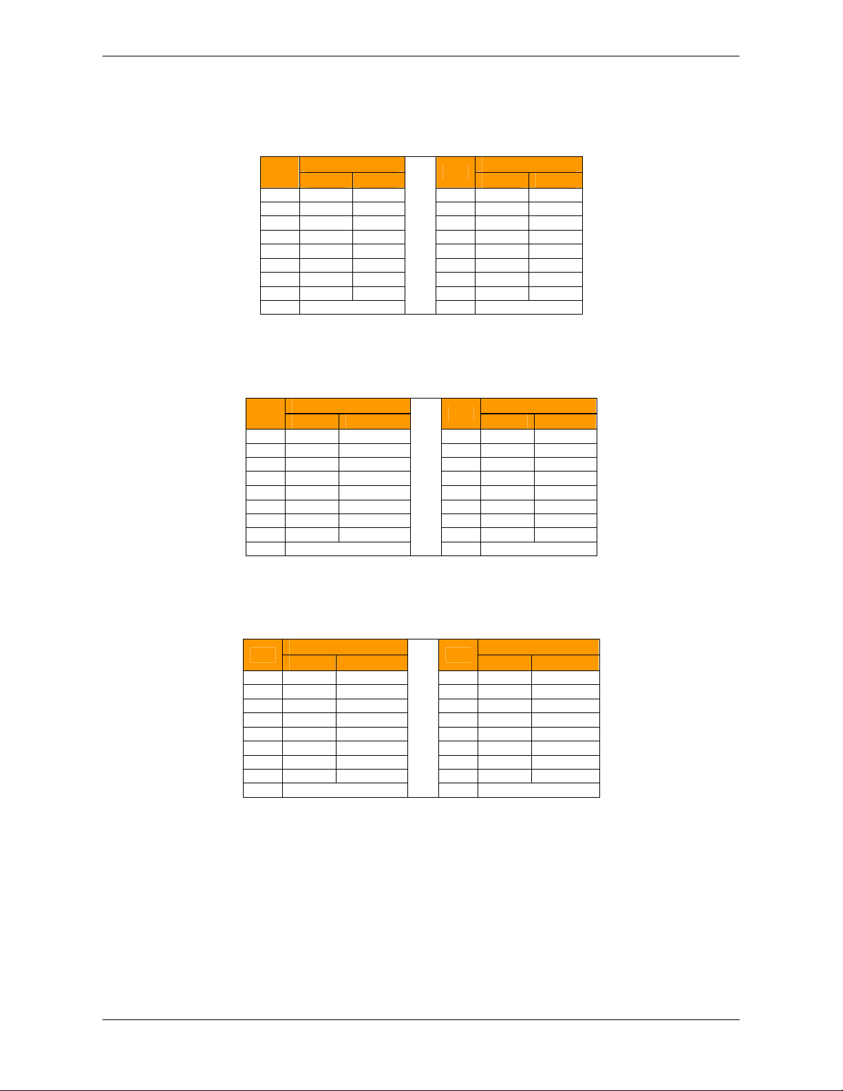
MPC5668EVB Users Manual Rev 0.1 May 2009
Function
Function
GPIO
1st
Alt GPIO
1st
Alt
Func
tion
Function
GPIO
1st
Alt GPIO
1st
Alt
11 PC10
AN42 12 PC11
AN43
Function
Function
GPIO
1st
Alt GPIO
1st
Alt
6.1.2 Port B / ADC / SPI (P18)
Table 6-3. Port B Connector Pinout (P18)
Pin
1 PB0 AN16 2 PB1 AN17
3 PB2 AN18 4 PB3 AN19
5 PB4 AN20 6 PB5 AN21
7 PB6 AN22 8 PB7 AN23
9 PB8 AN24 10 PB9 AN25
11 PB10 AN26 12 PB11 AN27
13 PB12 AN28 14 PB13 AN29
15 PB14 AN30 16 PB15 AN31
17 GND 18 GND
6.1.3 Port C / ADC / FLEXRAY / I2C (P19)
Table 6-4. Port C Connector Pinout (P19)
Pin
1 PC0 AN32 2 PC1 AN33
3 PC2 AN34 4 PC3 AN35
5 PC4 AN36 6 PC5 AN37
7 PC6 AN38 8 PC7 AN39
9 PC8 AN40 10 PC9 AN41
13 PC12 AN44 14 PC13 AN45
15 PC14 AN46 16 PC15 AN47
17 GND 18 GND
Pin
Pin
6.1.4 Port D / CAN / I2C / SCI (P20)
Table 6-5. Port D Connector Pinout (P20)
Pin
1 PD0 CNTX_A 2 PD1 CNRX_A
3 PD2 CNTX_B 4 PD3 CNRX_B
5 PD4 CNTX_C 6 PD5 CNRX_C
7 PD6 CNTX_D 8 PD7 CNRX_D
9 PD8 CNTX_E 10 PD9 CNRX_E
11 PD10 CNTX_F 12 PD11 CNRX_F
13 PD12 TXD_A 14 PD13 RXD_A
15 PD14 TXD_B 16 PD15 TXD_B
17 GND 18 GND
Pin
MPC5668EVBUM/D Page 29 of 29
Page 34
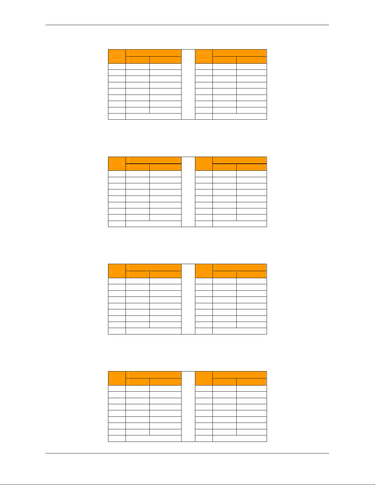
MPC5668EVB Users Manual Rev 0.1 May 2009
Function
Function
GPIO
1st
Alt GPIO
1st
Alt
Function
Function
GPIO
1
s
t
Alt GPIO
1st
Alt
Function
Function
GPIO
1st
Alt GPIO
1st
Alt
PCS_D[1
]
PCS_D[2
]
Function
Function
GPIO
1st
Alt GPIO
1st
Alt
eMIOS[27]
eMIOS[26]
eMIOS[23]
eMIOS[22]
eMIOS[17]
eMIOS[16]
6.1.5 Port E / SCI / eMIOS / I2C (P21)
Table 6-6. Port E Connector Pinout (P21)
Pin
1 PE0 TXD_C 2 PE1 RXD_C
3 PE2 TXD_D 4 PE3 RXD_D
5 PE4 TXD_E 6 PE5 RXD_E
7 PE6 TXD_F 8 PE7 RXD_F
9 PE8 TXD_G 10 PE9 RXD_G
11 PE10 TXD_H 12 PE11 RXD_H
13 PE12 TXD_J 14 PE13 RXD_J
15 PE14 SCL_A 16 PE15 SDA_A
17 GND 18 GND
6.1.6 Port F / DSPI (P26)
Pin
1 PF0 SCK_A 2 PF1 SOUT_A
3 PF2 SIN_A 4 PF3 PCS_A[0]
5 PF4 SCK_B 6 PF5 SOUT_B
7 PF6 SIN_B 8 PF7 PCS_B[0]
9 PF8 SCK_C 10 PF9 SOUT_C
11 PF10 SIN_C 12 PF11 PCS_C[0]
13 PF12 SCK_D 14 PF13 SOUT_D
15 PF14 SIN_D 16 PF15 PCS_D[0]
17 GND 18 GND
Pin
Table 6-7. Port F Connector Pinout (P26)
Pin
6.1.7 Port G / DSPI / eMIOS / FEC (P27)
Table 6-8. Port F Connector Pinout (P27)
Pin
1 PG0
3 PG2
5 PG4
7 PG6
9 PG8
11 PG10
13 PG12
15 PG14
17 GND 18 GND
PCS_A[4]
PCS_D[3]
PCS_C[1]
eMIOS[7]
eMIOS[5]
eMIOS[3]
eMIOS[1]
6.1.8 Port H / eMIOS / FEC (P28)
Table 6-9. Port H Connector Pinout (P28)
Pin
1 PH0
3 PH2
5 PH4
7 PH6
9 PH8
11 PH10
13 PH12
15 PH14
17 GND 18 GND
eMIOS[31]
eMIOS[29]
eMIOS[25]
eMIOS[21]
eMIOS[19]
Pin
2 PG1
4 PG3
6 PG5
8 PG7
10 PG9
12 PG11
14 PG13
16 PG15
Pin
2 PH1
4 PH3
6 PH5
8 PH7
10 PH9
12 PH11
14 PH13
16 PH15
PCS_A[5]
PCS_D[4]
PCS_C[2]
eMIOS[6]
eMIOS[4]
eMIOS[2]
eMIOS[0]
eMIOS[30]
eMIOS[28]
eMIOS[24]
eMIOS[20]
eMIOS[18]
MPC5668EVBUM/D Page 30 of 29
Page 35
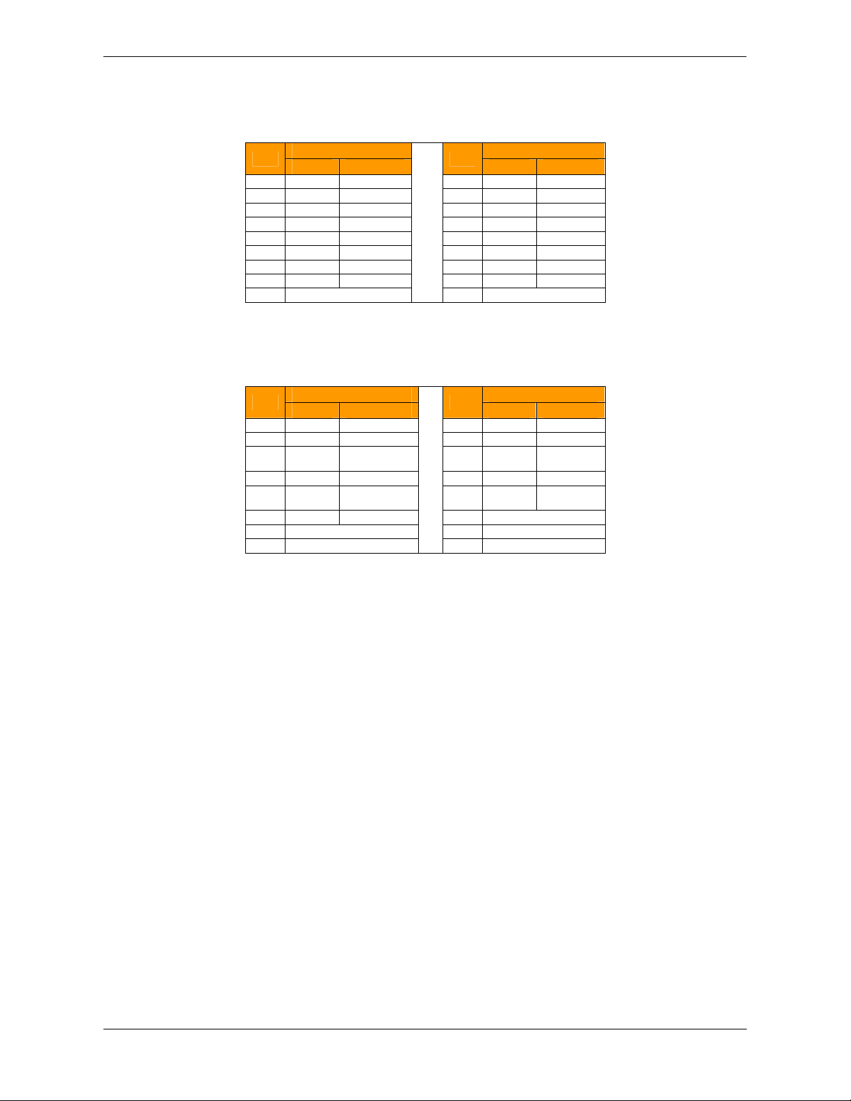
MPC5668EVB Users Manual Rev 0.1 May 2009
Function
Function
GPIO
1st
Alt GPIO
1st
Alt
eMIOS[13]
eMIOS[12
]
eMIOS[7]
eMIOS[6
]
eMIOS[3]
eMIOS[2
]
Function
Function
GPIO
1st
Alt GPIO
1st
Alt
MLBCLK
MLBSIG
FR_A_TX
EN
6.1.9 Port J / eMIOS / FEC (P29)
Table 6-10. Port J Connector Pinout (P29)
Pin
1 PJ0
3 PJ2
5 PJ4
7 PJ6
9 PJ8
11 PJ10
13 PJ12
15 PJ14
17 GND 18 GND
eMIOS[15]
eMIOS[11]
eMIOS[9]
eMIOS[5]
eMIOS[1]
6.1.10 Port K / RESET / MLB (Connector P30)
Table 6-11. Port K Connector Pinout (P30)
Pin
1 PK0
3 PK2
5 PK4
7 PK6
9 PK8
11 PK10
13
15 GND 16 GND
MLBDAT
FR_B_RX
FR_B_TX_E
N
PCS_B[5]
RST OUT
Pin
2 PJ1
4 PJ3
6 PJ5
8 PJ7
10 PJ9
12 PJ11
14 PJ13
16 PJ15
Pin
2 PK1
4 PK3
6 PK5
8 PK7
10 PK9
12
14
eMIOS[14]
eMIOS[10]
eMIOS[8]
eMIOS[4]
eMIOS[0]
FR_A_RX
FR_A_TX_
FR_B_TX
CLKOUT
GND
TST RST
MPC5668EVBUM/D Page 31 of 29
Page 36

MPC5668EVB Users Manual Rev 0.1 May 2009
6.2 Prototyping Area and
User LED’s / Switches
The prototyping area is
located on the right hand
side of the EVB, above the
user connectors.
There is a rectangular prototype area on the EVB, consisting of a 0.1inch pitch array of through-hole plated
pads. Power from all three voltage regulators is readily accessible along with GND. This area is ideal for the
addition of any custom circuitry. Adapters are available to convert SMD devices to 0.1inch pitch through-hole.
Some of the pads in the prototyping area are connected to the CAN C – F pins of the MCU as well as power
and the DB9 connectors. This allows an additional 4 CAN physical interfaces to be added to the EVB for
evaluation with the MCU. The layout of this is shown in Figure X below.
Note: The power supply lines to the prototype area are connected directly to the regulator outputs and not
connected to the jumpered MCU supply.
There are 4 active low user LED’s DS4, DS5, DS6 and DS7, These are driven by connecting a logic 0 signal
to the corresponding pin on 0.1” header P15 (user LED’s).
There are 4 active high pushbutton switches SW2, SW3, SW4 and SW5 which will drive 5V onto the
respective pins on 0.1” connector P16 when pressed. The switch outputs are pulled to GND with a 10K
resistor network.
MPC5668EVBUM/D Page 32 of 29
Page 37
MPC5668EVB Users Manual Rev 0.1 May 2009
Appendix A - EVB Schematics
MPC5568EVBUM/D Page A-1
Page 38
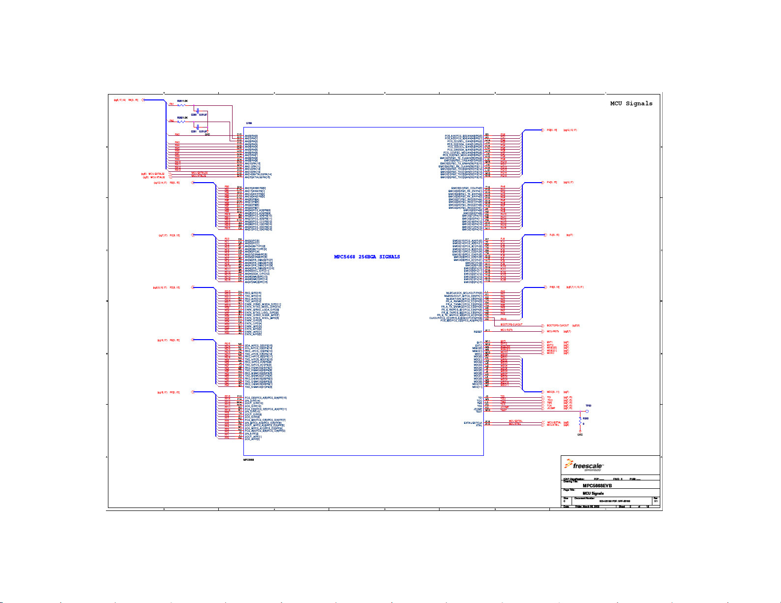
MPC5668EVB Users Manual Rev 0.1 May 2009
MPC5568EVBUM/D Page A-2
Page 39
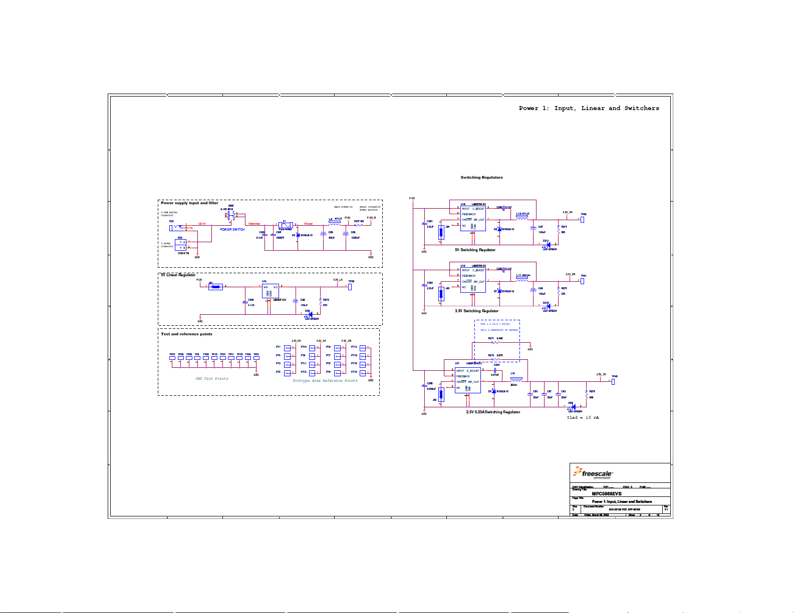
MPC5668EVB Users Manual Rev 0.1 May 2009
MPC5568EVBUM/D Page A-3
Page 40
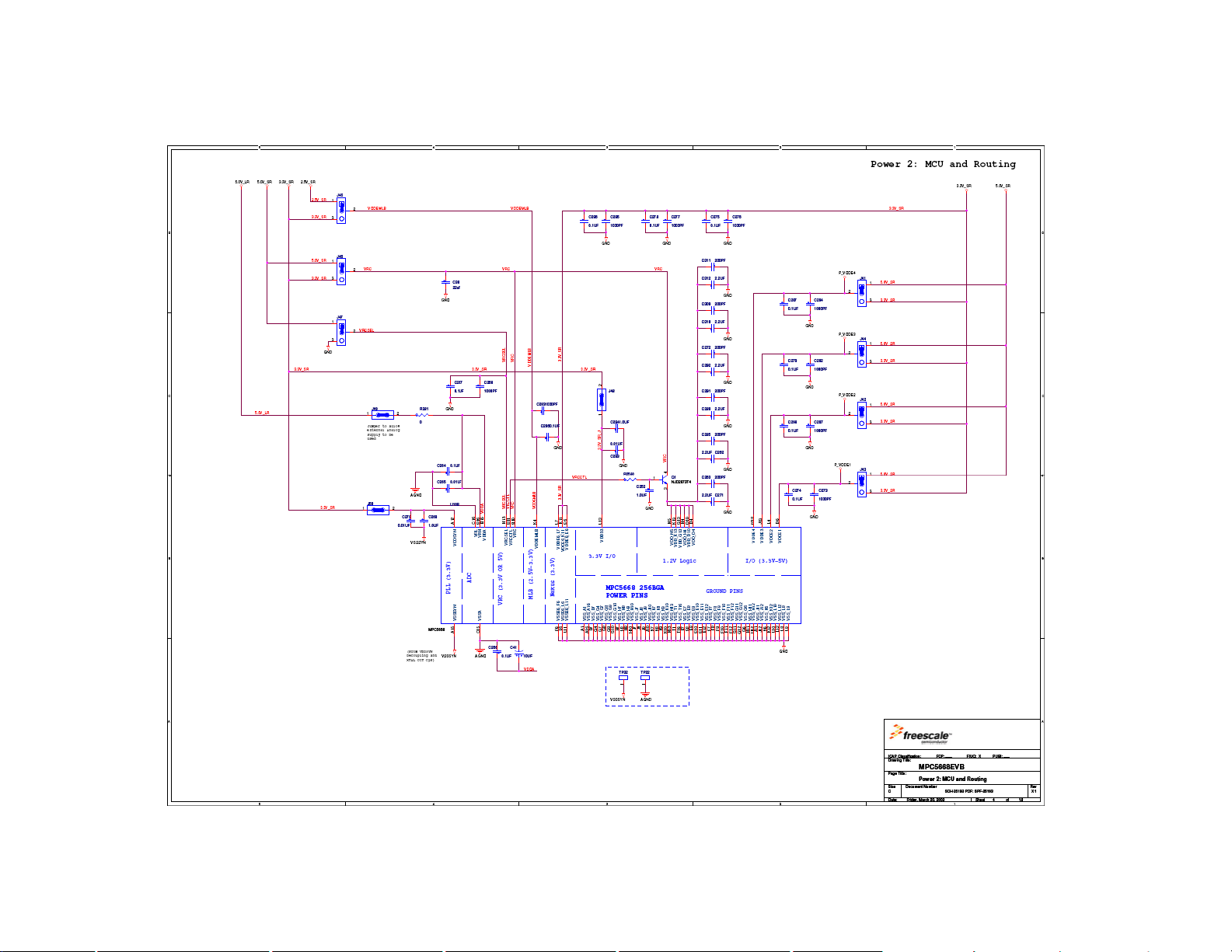
MPC5668EVB Users Manual Rev 0.1 May 2009
MPC5568EVBUM/D Page A-4
Page 41
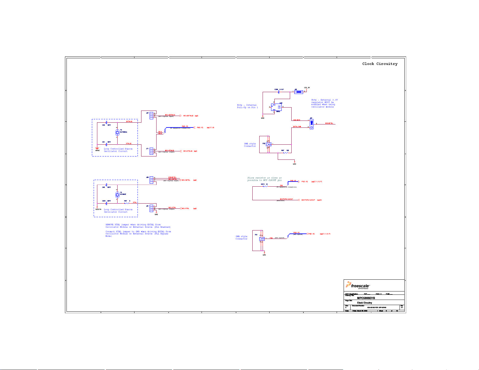
MPC5668EVB Users Manual Rev 0.1 May 2009
MPC5568EVBUM/D Page A-5
Page 42
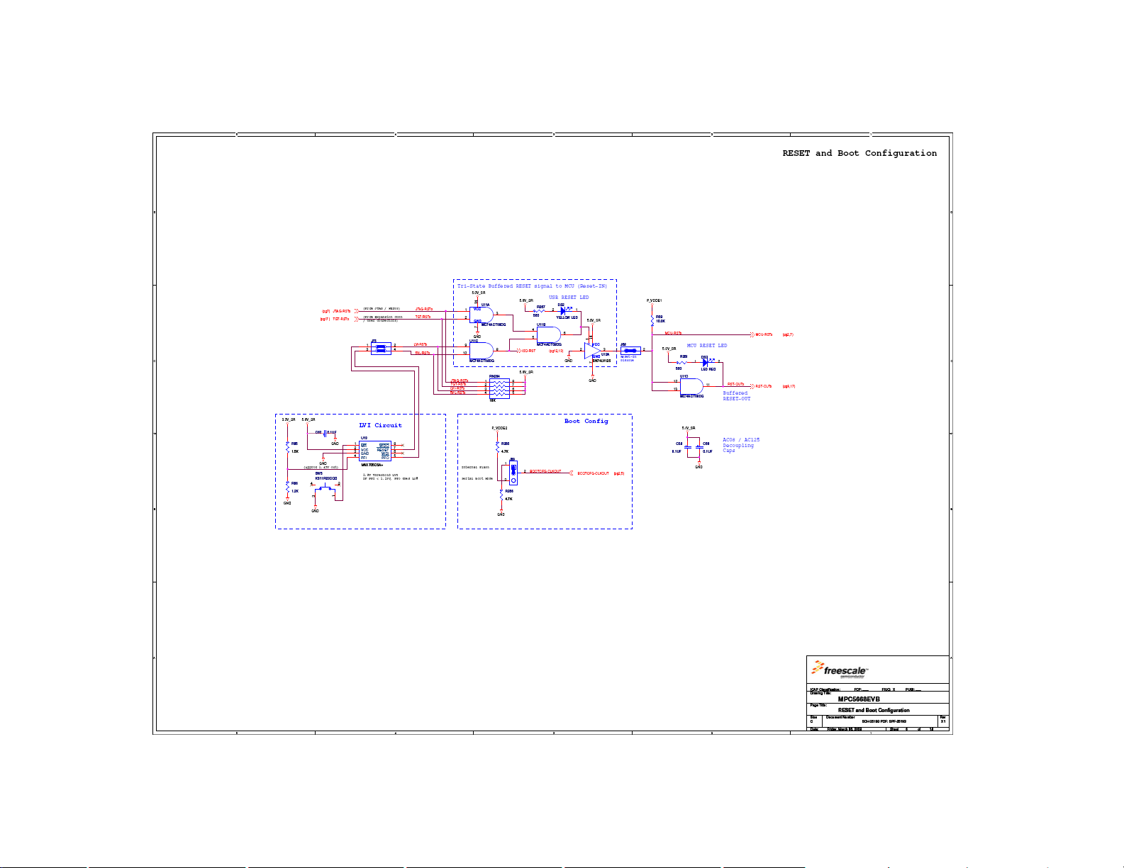
MPC5668EVB Users Manual Rev 0.1 May 2009
MPC5568EVBUM/D Page A-6
Page 43
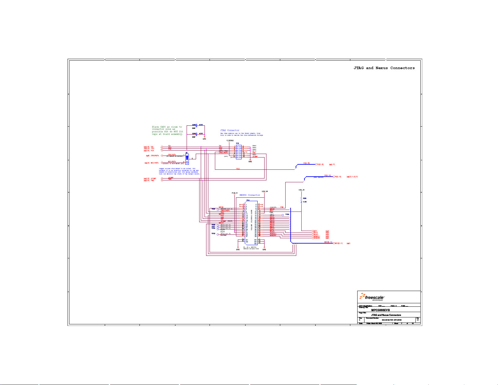
MPC5668EVB Users Manual Rev 0.1 May 2009
MPC5568EVBUM/D Page A-7
Page 44
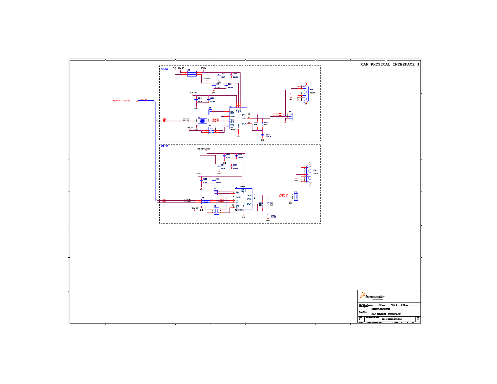
MPC5668EVB Users Manual Rev 0.1 May 2009
MPC5568EVBUM/D Page A-8
Page 45
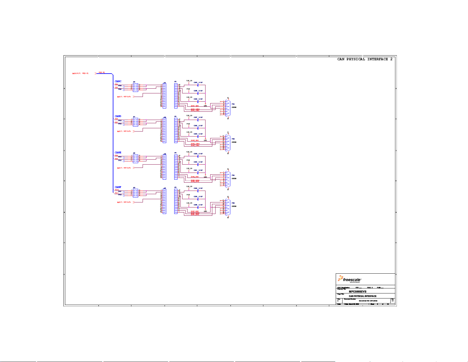
MPC5668EVB Users Manual Rev 0.1 May 2009
MPC5568EVBUM/D Page A-9
Page 46
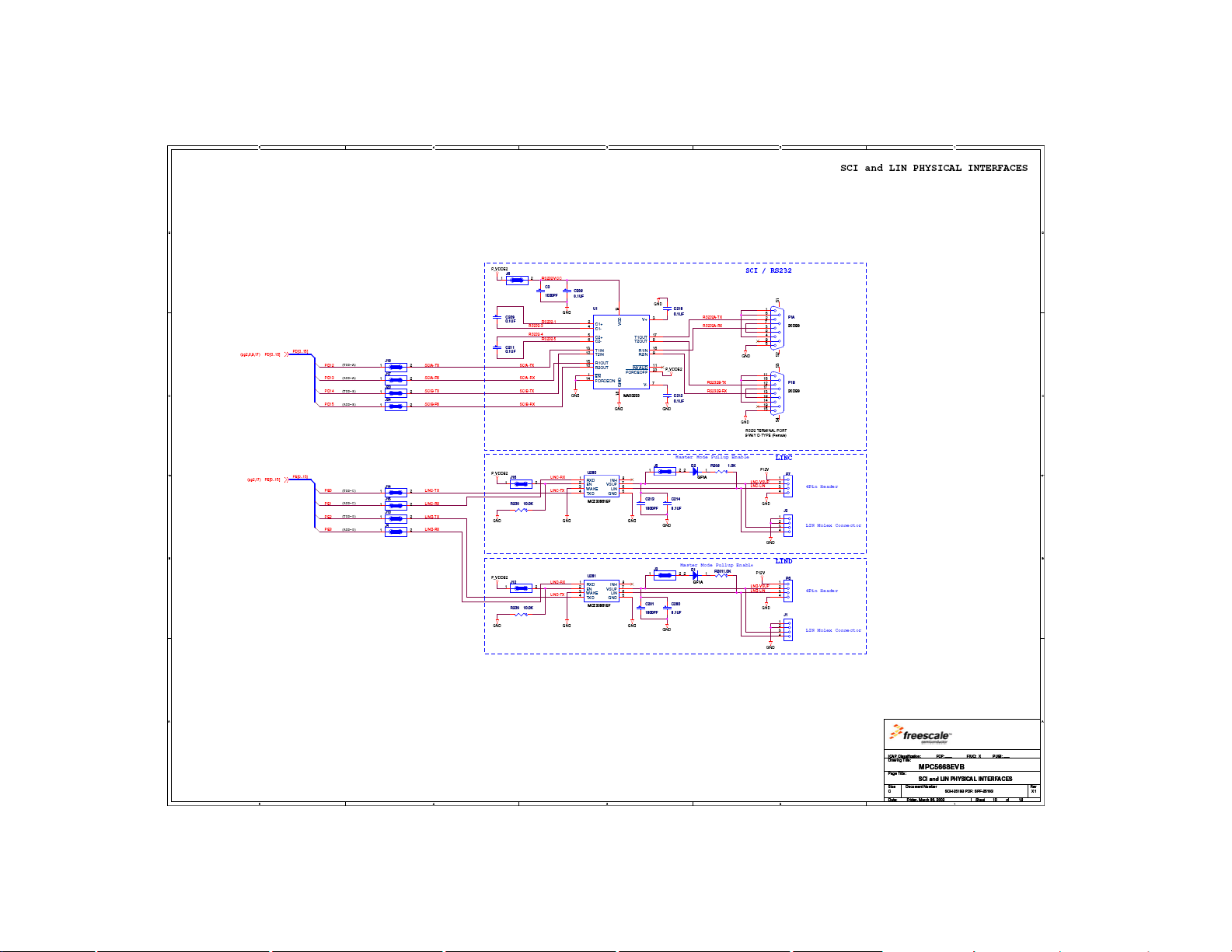
MPC5668EVB Users Manual Rev 0.1 May 2009
MPC5568EVBUM/D Page A-10
Page 47
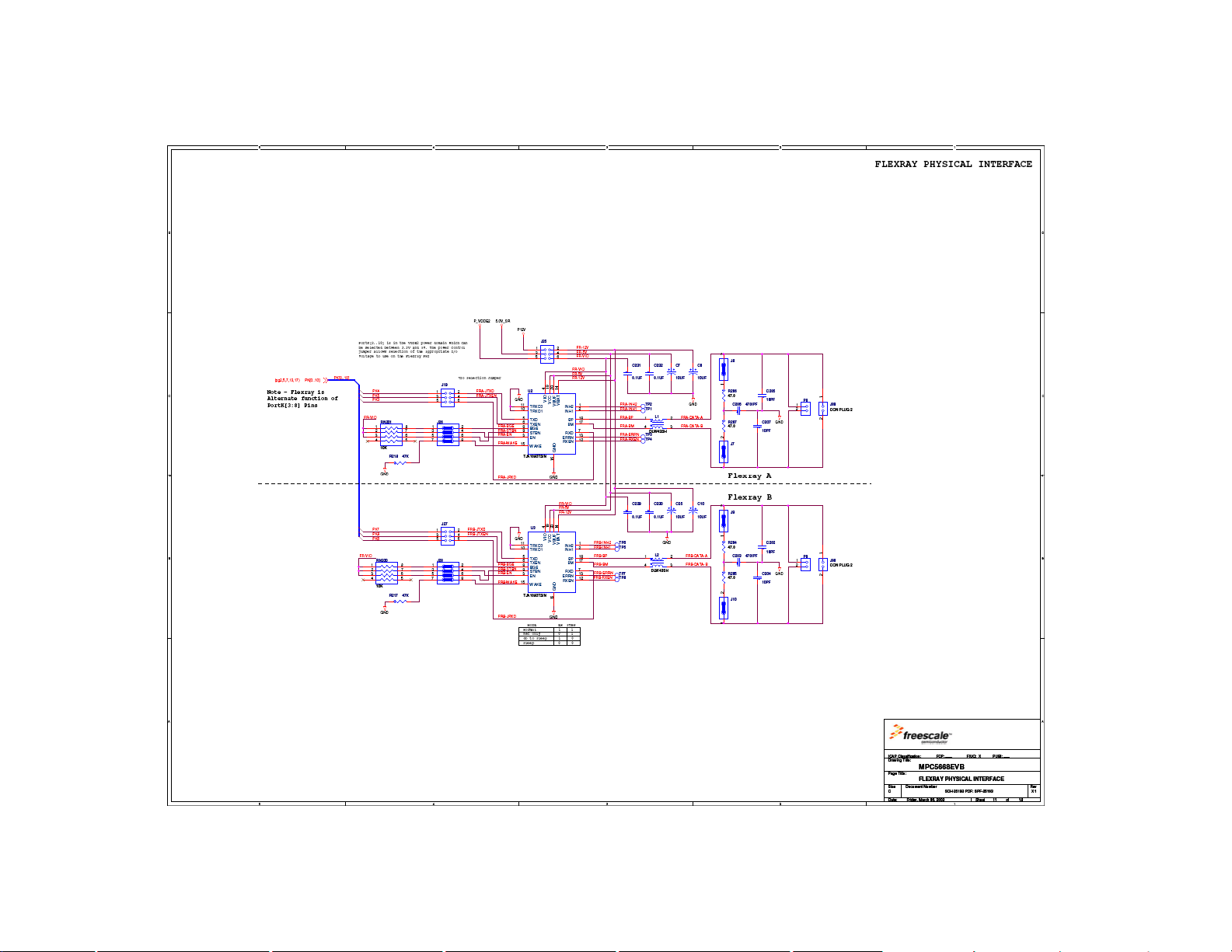
MPC5668EVB Users Manual Rev 0.1 May 2009
MPC5568EVBUM/D Page A-11
Page 48
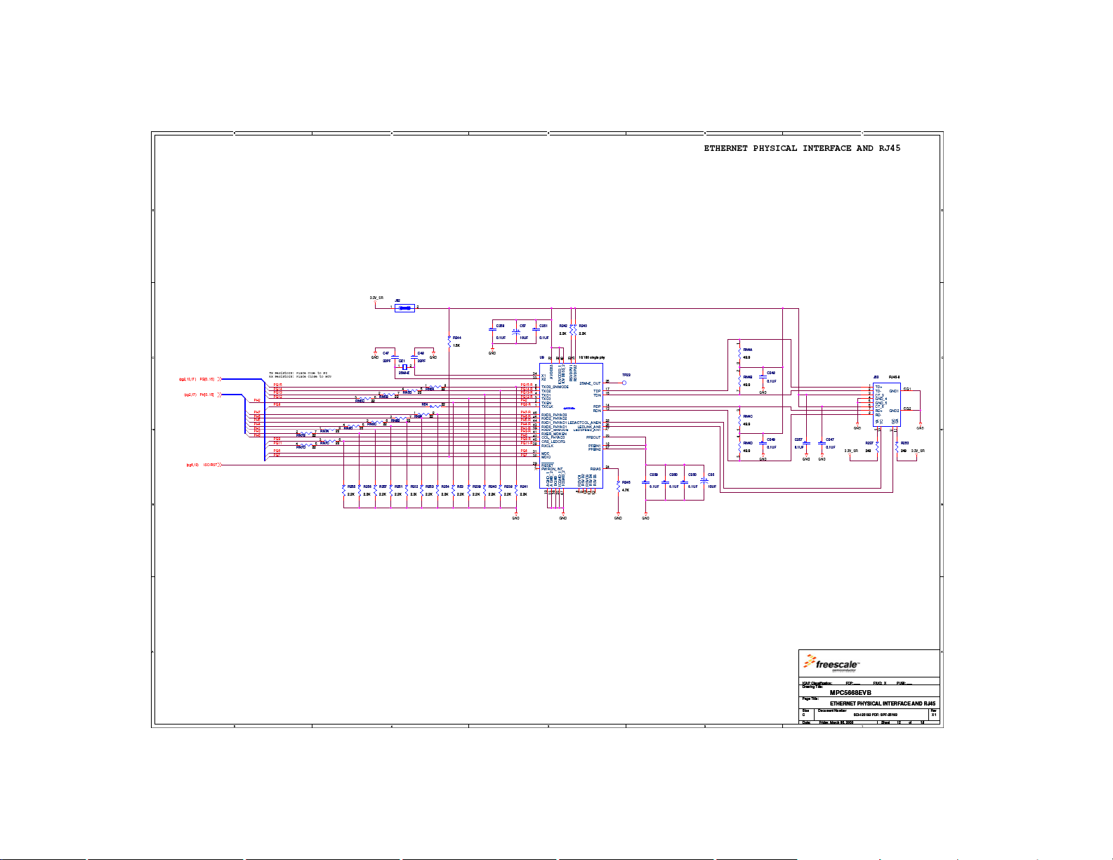
MPC5668EVB Users Manual Rev 0.1 May 2009
MPC5568EVBUM/D Page A-12
Page 49
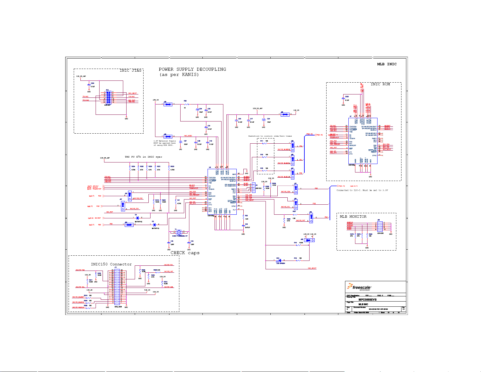
MPC5668EVB Users Manual Rev 0.1 May 2009
MPC5568EVBUM/D Page A-13
Page 50
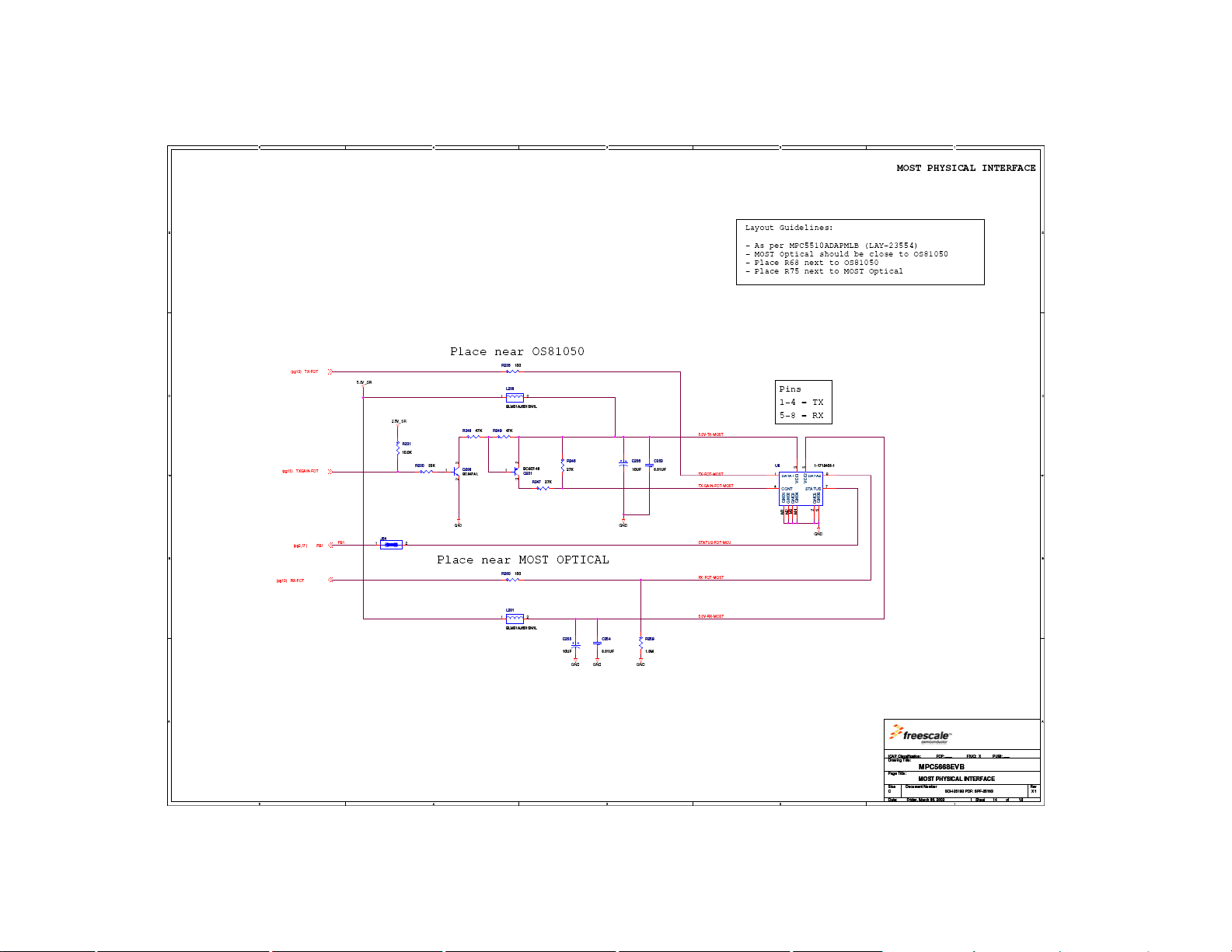
MPC5668EVB Users Manual Rev 0.1 May 2009
MPC5568EVBUM/D Page A-14
Page 51
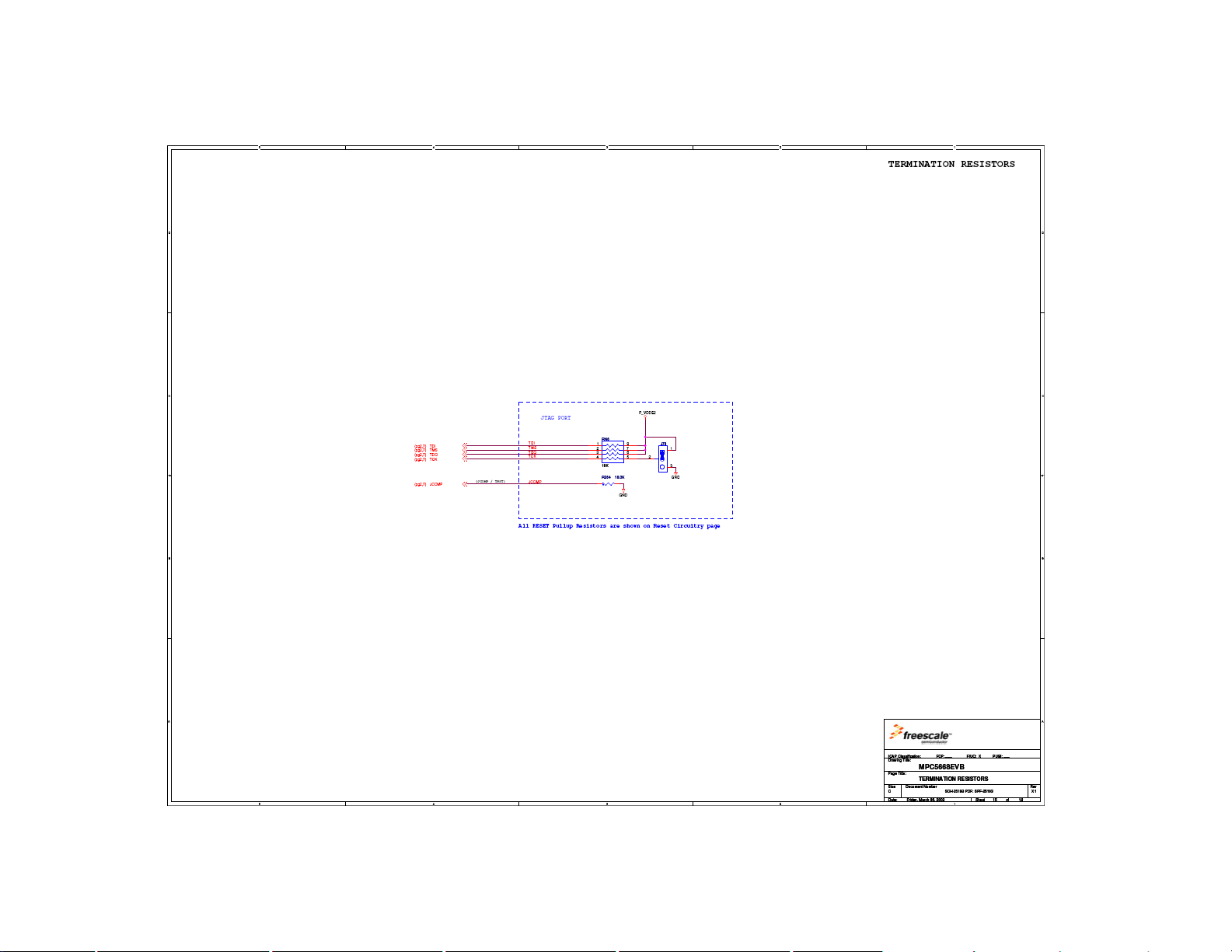
MPC5668EVB Users Manual Rev 0.1 May 2009
MPC5568EVBUM/D Page A-15
Page 52
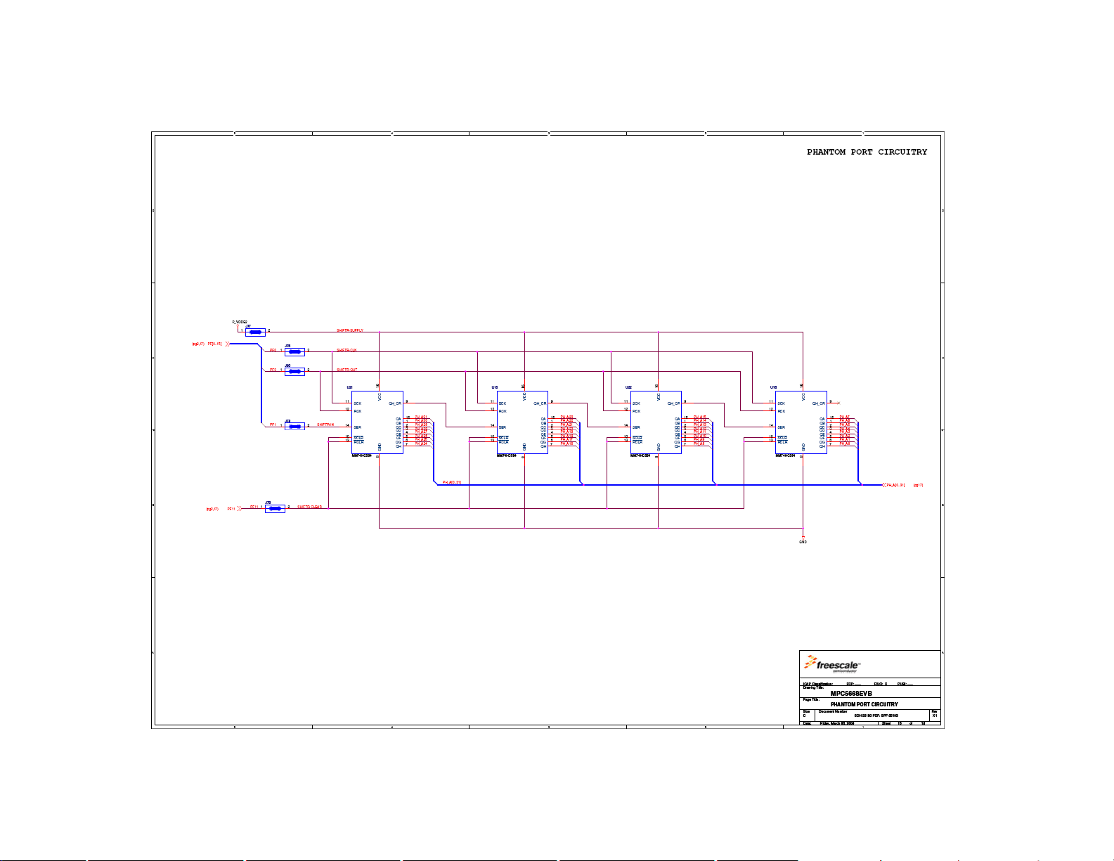
MPC5668EVB Users Manual Rev 0.1 May 2009
MPC5568EVBUM/D Page A-16
Page 53
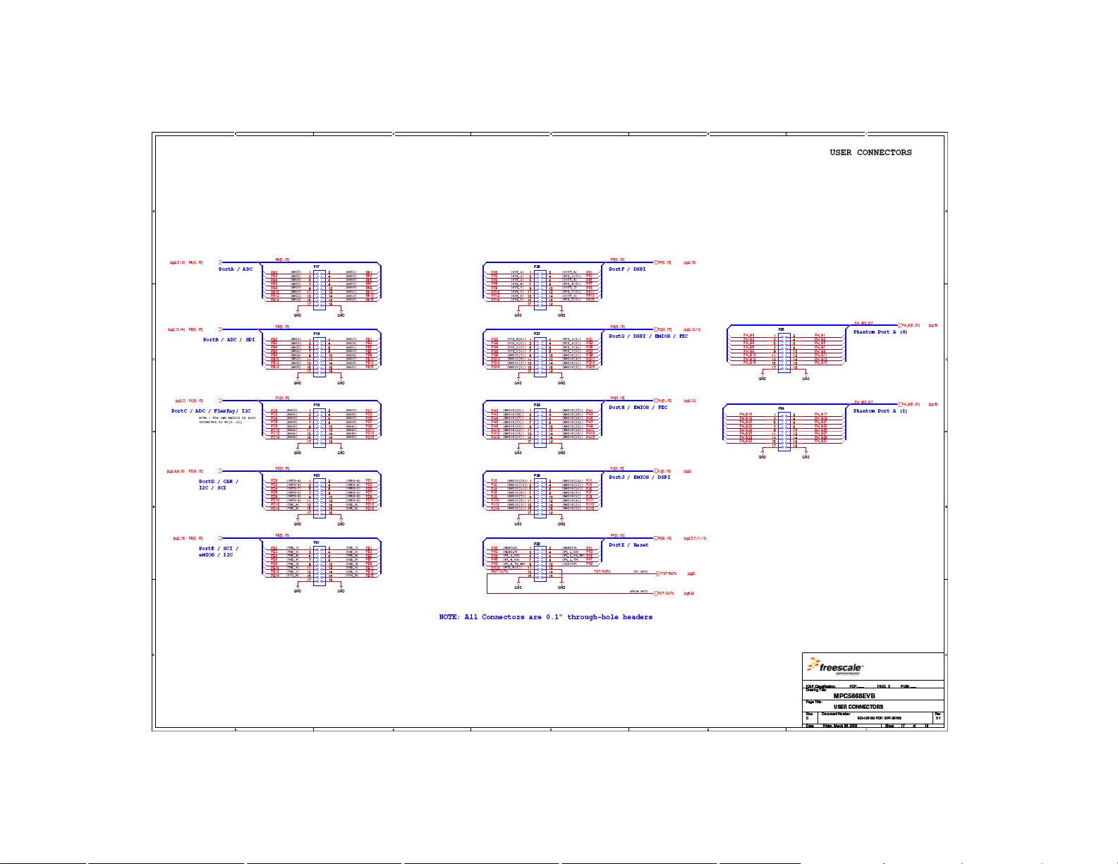
MPC5668EVB Users Manual Rev 0.1 May 2009
MPC5568EVBUM/D Page A-17
Page 54
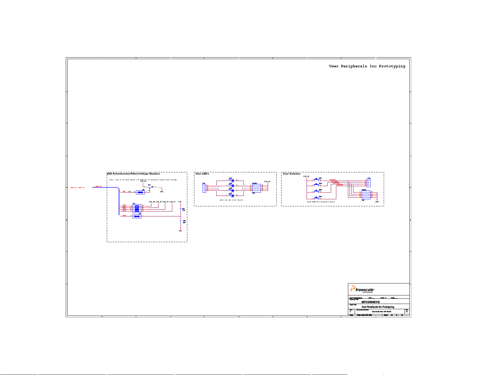
MPC5668EVB Users Manual Rev 0.1 May 2009
MPC5568EVBUM/D Page A-18
 Loading...