

Page 1

Freescale Semiconductor
MPC5607BRMAD
Reference Manual Addendum
MPC5607B Microcontroller
Reference Manual Addendum
by: Microcontroller Solutions Group
Rev. 1, 05/2012
This addendum document describes corrections to the
MPC5607B Microcontroller Reference Manual, order
number MPC5607BRM. For convenience, the addenda
items are grouped by revision. Please check our website
at http://www.freescale.com/powerarchitecture for the
latest updates.
The current version available of the MPC5607B
Microcontroller Reference Manual is Revision 7.1.
Table of Contents
1 Addendum List for Revision 7.1 . . . . . . . . . . . . . . 2
2 Revision History . . . . . . . . . . . . . . . . . . . . . . . . . 10
© Freescale Semiconductor, Inc., 2012. All rights reserved.
Page 2

Addendum List for Revision 7.1
1 Addendum List for Revision 7.1
Table 1. MPC5607BRM Rev 7.1 Addenda
Location Description
Chapter 1, Preface, page 22 In Table 1-1, Guide to this reference manual, Line 12 WKUP, change the description to read:
Always-active analog bloc k. Details configuration of 2 internal (API/RTC) and 27 external (pin)
low power mode wakeup sources.
Chapter 1, Preface, page 23 In Table 1 (Guide to this reference manual), Line 17, eDMA Channel Multiplexer (DMA_MUX),
change the description to read:
“Operation and configuration information for the eDMA multiplexer, which ta kes the 59
possible eDMA sources (triggers from the DSPI, eMIOS, I
multiplexes them onto the 16 eDMA channels.” (59 sources, 16 channels)
Chapter 1, Preface, page 27 In Section 1.6.1, The MPC5607B document set, remove bullet item
“e200z4 Power Architecture Core Reference Man ual.”
Chapter 1, Preface, page 27 In Section 1.6.1, The MPC5607B document set, change bullet item “Configuring CPU memory,
branch and cache optimizations” to “Configuring CPU memory and branch optimizations.”
Chapter 1, Preface, page 30 In Section 1.7.3, Software design, remov e the paragraph “The MMU translates physical memory
addresses for use by the CPU and it must be configured before any peripherals or memories
are available f or use by the CPU. See the e200z4 P ow er Architecture Core Reference Manual
for details on how to configure the MMU.”
Chapter 6, Clock Description,
page 132
Chapter 9, Reset Generation
Module (MC_RGM), page
232
Add Note: to Section 6.8.4.1, Crystal clock monitor:
Note: Functional FXOSC monitoring can only be guaranteed when the FXOSC frequency is
greater than (FIRC / 2
Add Note: to Section 6.8.4.2, FMPLL clock monitor:
Note: Functional FMPLL monitoring can only be guaranteed when the FMPLL frequency is
greater than (FIRC / 4) + 0.5 MHz.
Replaced Section 9.4.7, Boot Mode Capturing, with the following:
The MC_RGM samples P A[9:8] whenev er RESET is asserted until five FIRC (16 MHz internal
RC oscillator) clock cycles before its deassertion edge. The result of the sampling is used at
the beginning of reset PHASE3 for boot mode selection and is retained after RESET has been
deasserted for subsequent boots after reset sequences during which RESET is not asserted.
RCDIV
)+0.5MHz.
2
C, ADC and LINFlexD) and
Note: In order to ensure that the boot mode is correctly captured, the application needs to
apply the valid boot mode value the entire time that RESET is asserted.
RESET can be asserted as a consequence of the internal reset generation. This will force
re-sampling of the boot mode pins. (See Table 9-12 for details.)
Chapter 13, Real Time Clock /
Autonomous Periodic
Interrupt (RTC/API), page 270
In Table 13-3 (RTCC field descriptions), update the Note in the RTCC[APIVAL] field description:
Note: API functionality starts only when APIVAL is nonzero. The first API interrupt takes two
more cycles because of synchronization of APIVAL to the RTC cloc k, and APIVAL + 1 cycles
for subsequent occurrences. After that, interrupts are periodic in nature. Because of
synchronization issues, the minimum supported value of APIVAL is 4.
MPC5607B Reference Manual Errata, Rev. 1
Freescale Semiconductor2
Page 3

Table 1. MPC5607BRM Rev 7.1 Addenda (continued)
Table 16-24. Coherency model for a dynamic channel link request
Step Action
1 Write 1b to the TCD.major.e_link bit.
2 Read back the TCD.major.e_link bit.
3 Test the TCD.major.e_link request status:
• If TCD.major.e_link = 1b, the dynamic link attempt was successful.
• If TCD.major .e_link = 0b , the attempted dynamic link did not succeed (the channel
was already retiring).
Location Description
Addendum List for Revision 7.1
Chapter 16, Enhanced Direct
Memory Access (eDMA),
page 330
Replace Section 16.5.8, Dynamic programming, with the following:
16.5.8 Dynamic programming
16.5.8.1
Dynamic channel linking is the process of setting the TCD.major.e_link bit
during channel execution. This bit is read from the TCD local memory at the
end of channel execution, thus allowing the user to enable the feature during
channel execution.
Because the user is allowed to change the configuration during execution, a
coherency model is needed. Consider the scenario where the user attempts to
execute a dynamic channel link by enabling the TCD.major.e_link bit at the
same time the eDMA engine is retiring the channel. The TCD.major.e_link
would be set in the programmer’s model, but it would be unclear whether the
actual link was made before the channel retired.
The coherency model in Table 16-24 is recommended when executing a
dynamic channel link request.
Dynamic channel linking
For this request, the TCD local memory controller forces the TCD.major .e_link
bit to zero on any writes to a channel’s TCD.word7 after that channel’s
TCD.done bit is set, indicating the major loop is complete.
Freescale Semiconductor 3
NOTE
The user must clear the TCD.done bit before
writing the TCD.major .e_link bit. The TCD.done
bit is cleared automatically by the eDMA engine
after a channel begins execution.
MPC5607B Reference Manual Errata, Rev. 1
Page 4

Addendum List for Revision 7.1
Location Description
Table 1. MPC5607BRM Rev 7.1 Addenda (continued)
Chapter 16, Enhanced Direct
Memory Access (eDMA),
page 330 (cont.)
16.5.8.2 Dynamic scatter/gather
Dynamic scatter/gather is the process of setting the TCD.e_sg bit during
channel execution. This bit is read from the TCD local memory at the end of
channel execution, thus allowing the user to enable the feature during channel
execution.
Because the user is allowed to change the configuration during execution, a
coherency model is needed. Consider the scenario where the user attempts to
execute a dynamic scatter/gather operation by enabling the TCD.e_sg bit at the
same time the eDMA engine is retiring the channel. The TCD.e_sg would be
set in the programmer’s model, but it would be unclear whether the actual
scatter/gather request was honored before the channel retired.
T wo methods for this coherency model are shown in the following subsections.
Method 1 has the advantage of reading the major.linkch field and the e_sg bit
with a single read. For both dynamic channel linking and scatter/gather
requests, the TCD local memory controller forces the TCD.major.e_link and
TCD.e_sg bits to zero on any writes to a channel’ s TCD.word7 if that channel’ s
TCD.done bit is set indicating the major loop is complete.
NOTE
The user must clear the TCD.done bit before
writing the TCD.major .e_link or TCD.e_sg bits.
The TCD.done bit is cleared automatically by the
eDMA engine after a channel begins execution.
16.5.8.2.1 Method 1 (channel not using major loop channel
linking)
For a channel not using major loop channel linking, the coherency model in
Table 16-25 may be used for a dynamic scatter/gather request.
When the TCD.major .e_link bit is zero, the TCD.major.linkch field is not used
by the eDMA. In this case, the TCD.major.linkch bits may be used for other
purposes. This method uses the TCD.major .linkch field as a TCD identification
(ID).
MPC5607B Reference Manual Errata, Rev. 1
Freescale Semiconductor4
Page 5

Location Description
Table 16-25. Coherency model for method 1
Step Action
1 When the descriptors are built, write a unique TCD ID in the TCD .major .linkch field for
each TCD associated with a channel using dynamic scatter/gather.
2 Write 1b to theTCD.d_req bit.
Note: Should a dynamic scatter/gather attempt fail, setting the d_req bit will prevent a
future hardware activation of this channel. This stops the channel from
executing with a destination address (daddr) that was calculated using a
scatter/gather address (written in the next step) instead of a dlast final offset
value.
3 Write theTCD.dlast_sga field with the scatter/gather address.
4 Write 1b to the TCD.e_sg bit.
5 Read back the 16 bit TCD control/status field.
6 Test the TCD.e_sg request status and TCD.major.linkch value:
• If e_sg = 1b, the dynamic link attempt was successful.
• If e_sg = 0b and the major.linkch (ID) did not change, the attempted dynamic link
did not succeed (the channel was already retiring).
• If e_sg = 0b and the major.linkch (ID) changed, the dynamic link attempt was
successful (the new TCD’s e_sg value cleared the e_sg bit).
Chapter 16, Enhanced Direct
Memory Access (eDMA),
page 330 (cont.)
Addendum List for Revision 7.1
Table 1. MPC5607BRM Rev 7.1 Addenda (continued)
16.5.8.2.2 Method 2 (channel using major loop linking)
For a channel using major loop channel linking, the coherency model in
Table 16-26 may be used for a dynamic scatter/gather request. This method
uses the TCD.dlast_sga field as a TCD identification (ID).
For a channel using major loop channel linking, the coherency model in
Table 16-26 may be used for a dynamic scatter/gather request. This method
uses the TCD.dlast_sga field as a TCD identification (ID).
Freescale Semiconductor 5
MPC5607B Reference Manual Errata, Rev. 1
Page 6
Addendum List for Revision 7.1
Table 16-26.Coherency model for method 2
Step Action
1 Write 1b to theTCD.d_req bit.
Note: Should a dynamic scatter/gather attempt fail, setting the d_req bit will prevent a
future hardware activation of this channel. This stops the channel from
executing with a destination address (daddr) that was calculated using a
scatter/gather address (written in the next step) instead of a dlast final offset
value.
2 Write theTCD.dlast_sga field with the scatter/gather address.
3 Write 1b to the TCD.e_sg bit.
4 Read back the TCD.e_sg bit.
5 Test the TCD.e_sg request status:
• If e_sg = 1b, the dynamic link attempt was successful.
• If e_sg = 0b, read the 32 bit TCD dlast_sga field.
• If e_sg = 0b and the dlast_sga did not change, the attempted dynamic link did not
succeed (the channel was already retiring).
• If e_sg = 0b and the dlast_sga changed, the dynamic link attempt was successful
(the new TCD’s e_sg value cleared the e_sg bit).
CPU
Crossbar Switch
Flash
Master modules
Slave modules
CPU data
Internal
Peripheral
bridges
instructions
memory
SRAM
eDMA
Module
Port
Physical master ID
Type Logical number
eDMA Master 1 2
Location Description
Chapter 16, Enhanced Direct
Memory Access (eDMA),
page 330 (cont.)
Table 1. MPC5607BRM Rev 7.1 Addenda (continued)
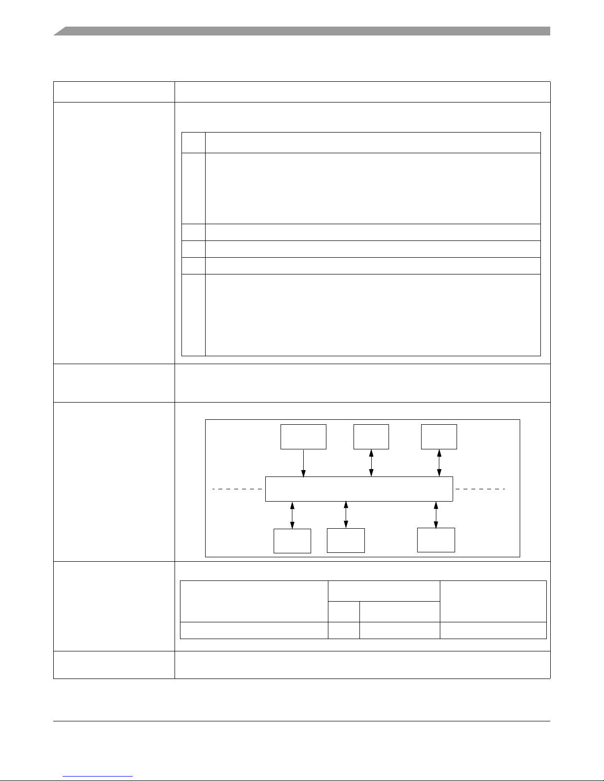
Chapter 19, Crossbar Switch
Correct “two master ports” to “three master ports” as necessary.
(XBAR), throughout
chapter
Chapter 19, Crossbar Switch
Replace Figure 19-1 (XBAR block diagram) with the following.
(XBAR), page 379
Chapter 19, Crossbar Switch
Add the following row for eDMA to Table 19-1 (XBAR switch port s for MPC5607B).
(XBAR), page 379
Chapter 19, Crossbar Switch
(XBAR), page 380
In Section 19.4, Features, add a bullet item for eDMA.
MPC5607B Reference Manual Errata, Rev. 1
Freescale Semiconductor6
Page 7

Table 1. MPC5607BRM Rev 7.1 Addenda (continued)
Table 19-2. Hardwired bus master priorities
Module
Port
Priority level
Type Master #
e200z0 core–CPU instructions Master 0 7
e200z0 core–CPU data Master 1 6
eDMA Master 2 5
Location Description
Addendum List for Revision 7.1
Chapter 19, Crossbar Switch
(XBAR), page 382
Chapter 20, Memory
Protection Unit (MPU),
page 389
Chapter 23, LINFlex, p. 494 Insert the following after Section 20.8.2.1.6, Error handling:
Replace Table 19-2 (Hardwired bus master priorities) with the following.
In Section 20.5.2.1 MPU Control/Error Status Register (MPU_CESR), in Figure 20-2 (MPU
Control/Error Status Register (MPU_CESR)), expand the SPERR field to an 8-bit field
stretching from bit 0 to bit 7.
23.8.2.1.6 Overrun
Once the message buffer is full, the next valid message reception leads to an
overrun and a message is lost. The hardware sets the BOF bit in the LINSR to
signal the overrun condition. Which message is lost depends on the
configuration of the RX message buffer:
• If the buffer lock function is disabled (LINCR1[RBLM] = 0) the last
message stored in the buffer is overwritten by the new incoming
message. In this case the latest message is always available to the
application.
• If the buffer lock function is enabled (LINCR1[RBLM] = 0) the most recent
message is discarded and the previous message is available in the buffer.
Chapter 24, LINFlexD, p. 514 Insert the following after Section 24.7.1.5, Error handling and detection:
21.7.1.6 Overrun
Once the message buffer is full, the next valid message reception leads to an
overrun and a message is lost. The hardware sets the BOF bit in the LINSR to
signal the overrun condition. Which message is lost depends on the
configuration of the RX message buffer:
• If the buffer lock function is disabled (LINCR1[RBLM] = 0) the last
message stored in the buffer is overwritten by the new incoming
message. In this case the latest message is always available to the
application.
• If the buffer lock function is enabled (LINCR1[RBLM] = 0) the most
recent message is discarded and the previous message is available in the
Freescale Semiconductor 7
buffer.
MPC5607B Reference Manual Errata, Rev. 1
Page 8

Addendum List for Revision 7.1
Location Description
Table 1. MPC5607BRM Rev 7.1 Addenda (continued)
Chapter 25, FlexCAN,
throughout chapter
Chapter 25, FlexCAN, page
594
Chapter 25, FlexCAN, page
596
Chapter 25, FlexCAN, page
619
Chapter 25, FlexCAN, page
624
Chapter 25, FlexCAN, page
629
Chapter 25, FlexCAN, page
631
Remove references throughout the chapter to “low-cost MCUs.”
Remove Note: above Table 25-2:
Note: The individual Rx Mask per Message Buffer feature may not be available in low cost
MCUs. Please consult the specific MCU documentation to find out if this feature is supported.
If not supported, the address range 0x0880-0x097F is considered reserved space,
independent of the value of the BCC bit.
Added this Note in the RTR field description of Table 25-4 (Message Buffer Structure field
description):
Note: Do not configure the last Message Buffer to be the RTR frame.
Remove Note: in Section 25.4.4.13 Rx Individual Mask Registers (RXIMR0–RXIMR63):
Note: The individual Rx Mask per Message Buffer feature may not be available in low cost
MCUs. Please consult the specific MCU documentation to find out if this feature is supported.
If not supported, the RXGMASK, RX14MASK and RX15MASK registers are available,
regardless of the value of the BCC bit.
Remove Note: at end of Section 25.5.6, Matching process:
Note: The individual Rx Mask per Message Buffer feature may not be available in low cost
MCUs. Please consult the specific MCU documentation to find out if this feature is supported.
If not supported, the RXGMASK, RX14MASK, and RX15MASK registers are available,
regardless of the value of the BCC bit.
In Section 25.5.9.4, Protocol timing, update the Note following Figure 25-16 (CAN Engine
Clocking Scheme) to read: “This clock selection feature may not be available in all MCUs. A
particular MCU may not have a PLL, in which case it would have only the oscillator clock, or
it may use only the PLL clock feeding the FlexCAN module. In these cases, the CLK_SRC bit
in the CTRL Register has no effect on the module operation.”
Update the table title of Table 25-22 from “CAN Standard Compliant Bit Time Segment Settings”
to “Bosch CAN 2.0B standard compliant bit time segment settings.”
Chapter 25, FlexCAN, page
631
Chapter 28, Analog-to-Digital
Converter (ADC), page 771
Chapter 28, Analog-to-Digital
Converter (ADC), page 772
In Section 25.5.9.4, Protocol timing, update the Note following Table 25-22 to read: “Other
combinations of Time Segment 1 and Time Segment 2 can be valid. It is the user’s
responsibility to ensure the bit time settings are in compliance with the CAN standard. For bit
time calculations, use an IPT (Information Processing Time) of 2, which is the value
implemented in the FlexCAN module.”
In Section 28.3.4.2, CTU in trigger mode, replace the sentence:
If another CTU conversion is triggered before the end of the conversion, that request is
discarded.
with:
If another CTU conversion is triggered before the end of the conversion, that request is
discarded. However, if the CTU has triggered a conversion that is still ongoing on a channel,
it will buffer a second request fo r the channel and wait for the end of the first conv ersion before
requesting another conversion. Thus, two conversion requests close together will both be
serviced.
In Section 28.3.5.2, Presampling channel enable signals, in Table 28-7, Presampling voltage
selection based on PREVALx fields, in the 01 row, change the “Presampling voltage” field to:
V1 = V
DD_HV_ADC0
or V
DD_HV_ADC1
.
MPC5607B Reference Manual Errata, Rev. 1
Freescale Semiconductor8
Page 9
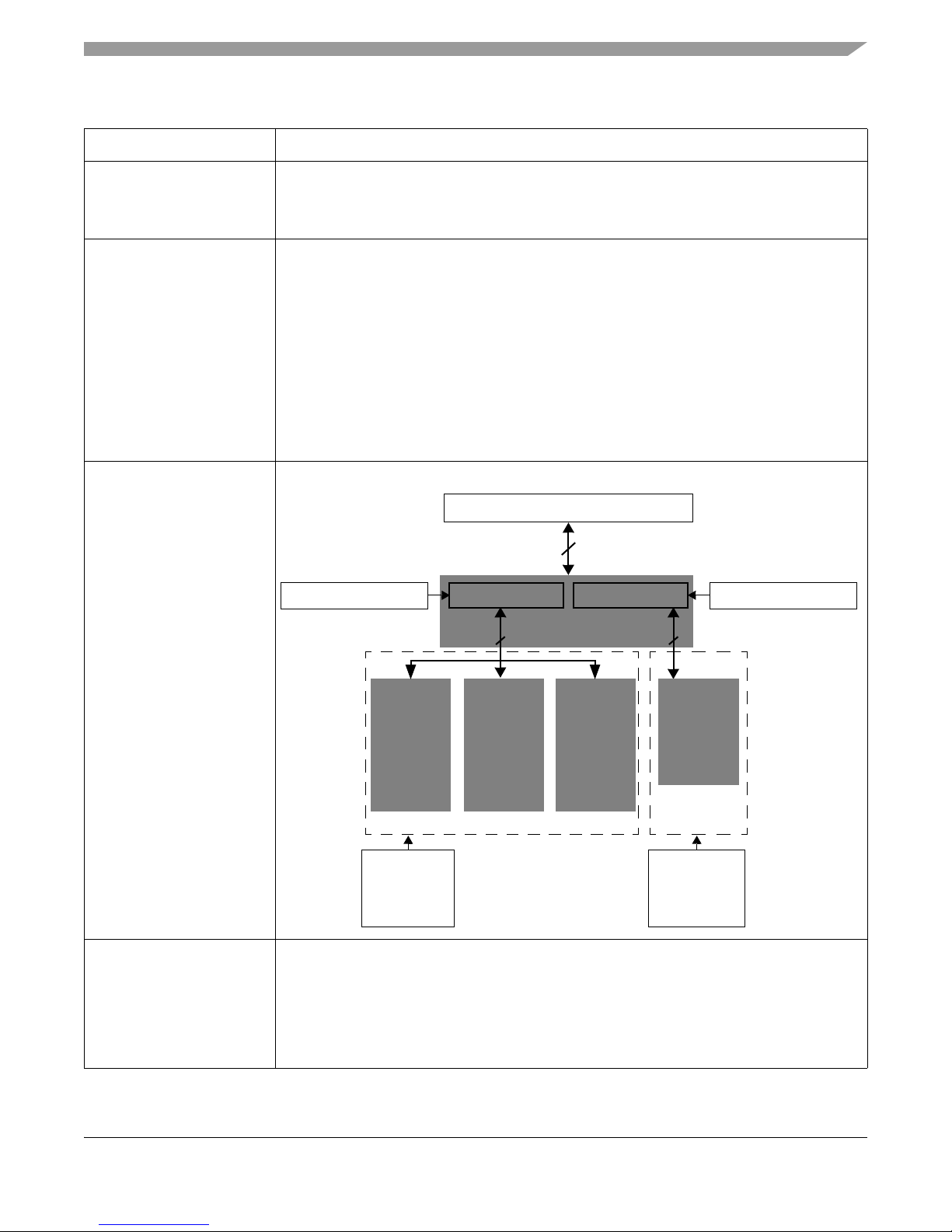
Table 1. MPC5607BRM Rev 7.1 Addenda (continued)
Crossbar switch
Bank0 (CFlash) Bank1 (DFlash)
32
data
(for EEPROM
Array 0
512 KB
Array 1
1x128 page buffer4x128 page buffer
PFlash controller
emulation)
CFLASH_PFCR0[B0_P0_BFE]
CFLASH_MCR
...
...
...
CFLASH_UMISR4
CFLASH_PFCR1[B1_P0_BFE]
DFLASH_MCR
...
...
...
DFLASH_UMISR4
Flash memory
flash memory
128 128
64 KB
Bank0 (CFlash)
512 KB
Array 2
Flash memory
Bank0 (CFlash)
512 KB
Array 0
Flash memory
Location Description
Addendum List for Revision 7.1
Chapter 28, Analog-to-Digital
Converter (ADC), page 776
Chapter 29, Cross Triggering
Unit (CTU), page 825
Chapter 30, Flash Memory,
page 833
Add Note to Section 28.3.11, Auto-clock-off mode:
Note: The auto-clock-off feature cannot operate when the digital interface runs at the same
rate as the analog interface. This means that when MCR.ADCCLKSEL = 1, the analog clock
will not shut down in IDLE mode.
At the end of Section 29.4.1, Event Configuration Registers (CTU_EVTCFGRx) (x = 0...63), add
the following Note:
NOTE
The CTU tracks issued conversion requests to the ADC. When the ADC
is being triggered by the CTU and there is a need to shut down the ADC,
the ADC must be allowed to complete conversions before being shut
down. This ensures that the CTU is notified of completion; if the ADC
is shut down while performing a CTU-triggered conversion, the CTU is
not notified and will not be able to trigger further conversions until the
device is reset.
Replace Figure 30-1. Flash memory architecture with the following.
Chapter 31, Static RAM
In Table 31-2, Low power configuration, in the STANDBY line, change the description
(SRAM), page 933
“Either all or just 8 KB of the SRAM remains powered. This option is software-selectable.”
Freescale Semiconductor 9
to
“Either 32 KB or just 8 KB of the SRAM remains powered. This option is software-selectable. ”
MPC5607B Reference Manual Errata, Rev. 1
Page 10

Revision History
Location Description
Table 1. MPC5607BRM Rev 7.1 Addenda (continued)
Chapter 32, Register
Protection, page 954
In Table 32-5, Protected registers, change the module base address for the CMU_CSR register
from C3FE00E0 to C3FE0000.
2 Revision History
Table 3 provides a revision history for this reference manual addendum document.
Table 2. Revision History Table
Rev. Number Substantive Changes Date of Release
1.0 • Initial release. 05/2012
MPC5607B Reference Manual Errata, Rev. 1
Freescale Semiconductor10
 Loading...