

Page 1

Freescale Semiconductor
User’s Guide
Document Number:
MPC5606SDEMOUG
Rev. 0, 10/2010
MPC5606S-DEMO-V2 User Guide
by: Ioseph Martinez
Freescale Applications Engineer
Tlaquepaque, Jalisco
1 Overview
The MPC56xxS family is the latest generation of 32-bit
Power Architecture microcontrollers (MCUs) that
address color thin-film transistor (TFT) displays in
automotive instrument cluster applications. It offers a
cost-effective entry-level instrument cluster solution
with the ability to scale your designs to fit your
performance needs.
1.1 Specific MPC5606S Key Features
• e200 32-bit Book E compliant CPU core
complex built on Power Architecture technology
• Display Control Unit (DCU) for direct drive of
TFT displays up to WQVGA resolution
• Stepper motor drivers (for driving up to six
instrumentation gauges)
• 40 x 4 segment LCD display driver
Contents
1 Overview . . . . . . . . . . . . . . . . . . . . . . . . . . . . . . . . . . . . . 1
2 Power . . . . . . . . . . . . . . . . . . . . . . . . . . . . . . . . . . . . . . . 3
3 Video . . . . . . . . . . . . . . . . . . . . . . . . . . . . . . . . . . . . . . . . 4
4 Input/Output. . . . . . . . . . . . . . . . . . . . . . . . . . . . . . . . . . . 5
5 Memory . . . . . . . . . . . . . . . . . . . . . . . . . . . . . . . . . . . . . . 7
6 Communications . . . . . . . . . . . . . . . . . . . . . . . . . . . . . . . 7
7 Debug . . . . . . . . . . . . . . . . . . . . . . . . . . . . . . . . . . . . . . . 9
8 Sound . . . . . . . . . . . . . . . . . . . . . . . . . . . . . . . . . . . . . . . 9
9 Initialization Code . . . . . . . . . . . . . . . . . . . . . . . . . . . . . . 9
© Freescale Semiconductor, Inc., 2010. All rights reserved.
Page 2
Overview
• 1 MB on-chip flash with separate 64 k Data Flash for the EEPROM Emulation
• 48 KB on-chip SRAM with ECC
• 160 KB on-chip graphics SRAM (no ECC)
• Parallel Data Interface (PDI) for digital video input
• Sound generation and playback using PWM channels and DMA
• QuadSPI Serial Flash Controller
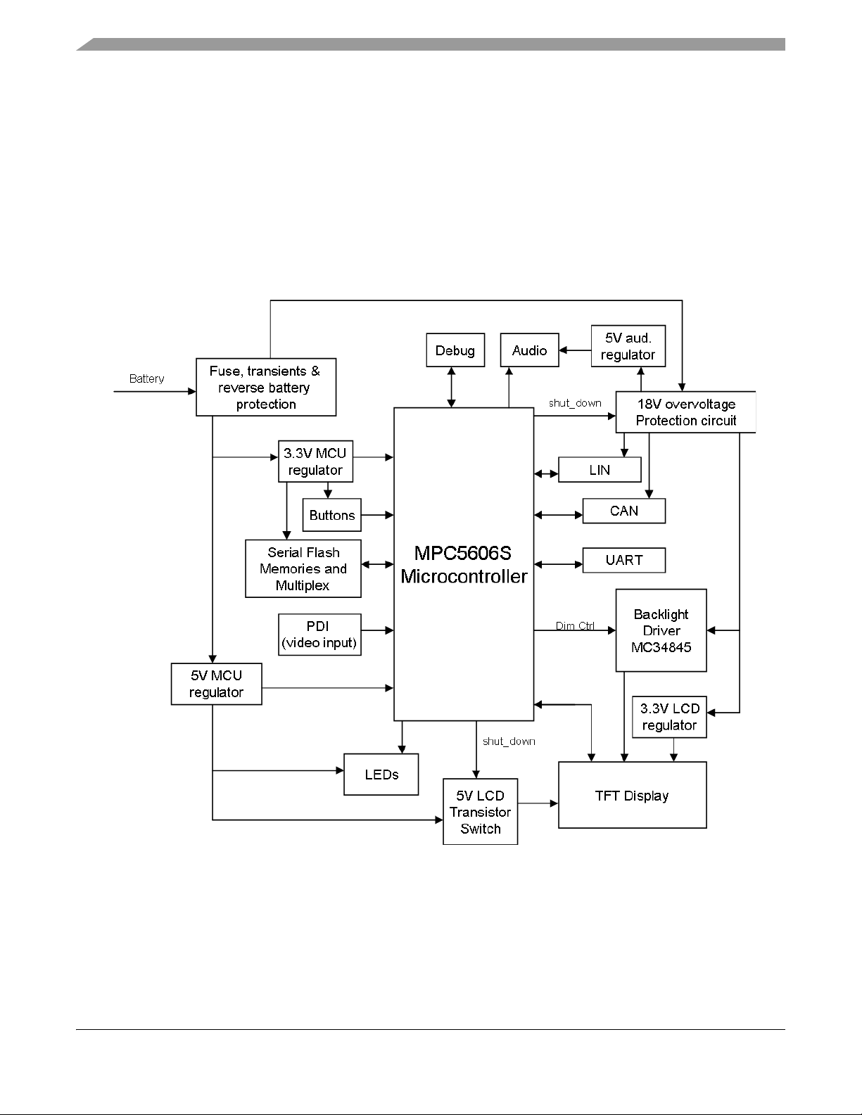
The MPC5606S-DEMO-V2 allows testing most of the MPC5606S MCUs features, especially graphics.
The following block diagram shows the functionality and architecture of the board.
Figure 1-1. MPC5606S-DEMO-V2 block diagram
MPC5606S-DEMO-V2 User Guide, Rev. 0
Freescale Semiconductor2
Page 3
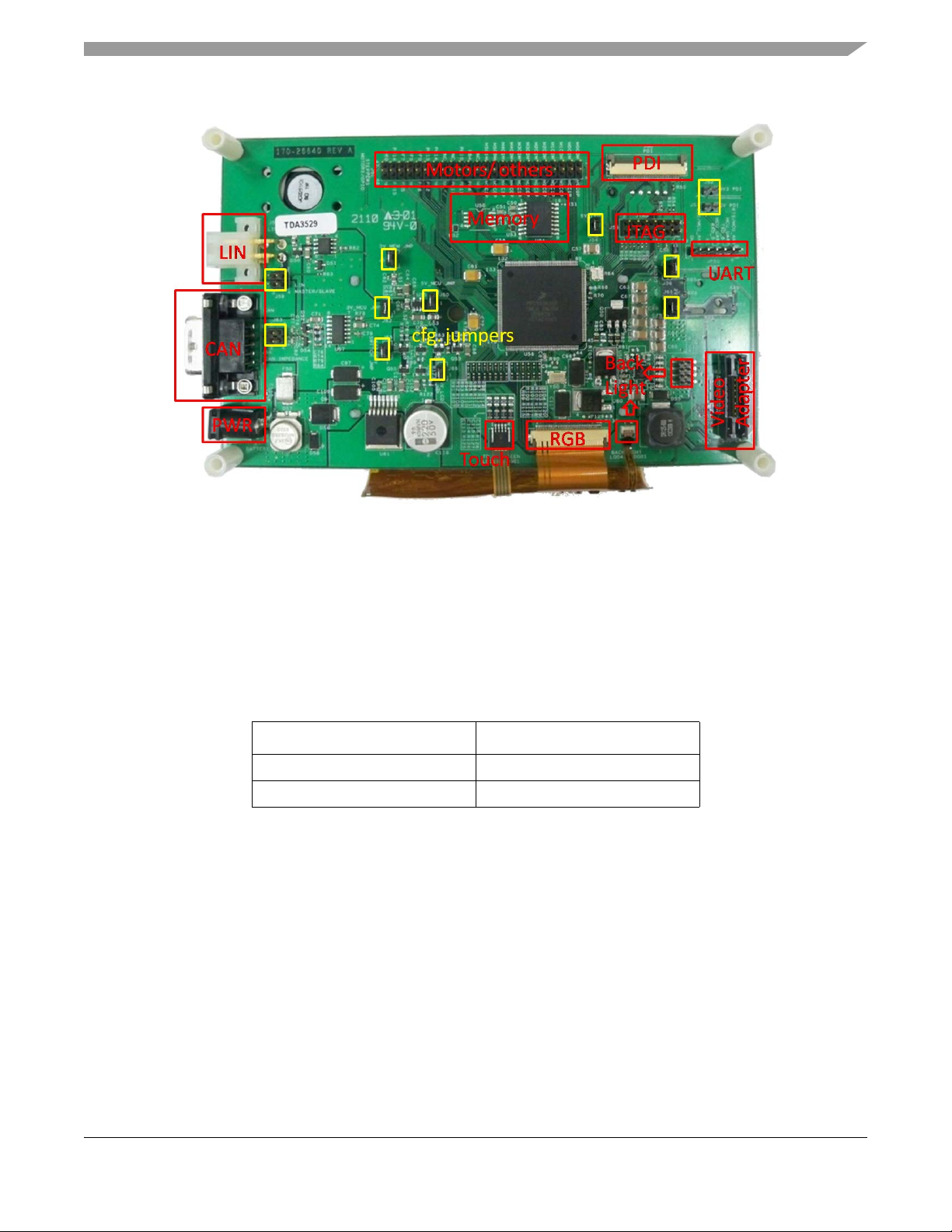
Figure 1-2. MPC5606S-DEMO-V2 functional blocks
Power
2Power
Power to the MPC5606S-DEMO-V2 is applied through a 2.1 mm center-positive barrel jack marked J69.
It includes a resettable poly-fuse F50 that provides protection from excessive current. A Transient Voltage
Suppression (TVS) device provides input protection from excessive voltage. Table 2-1 shows the input
voltages accepted by the board.
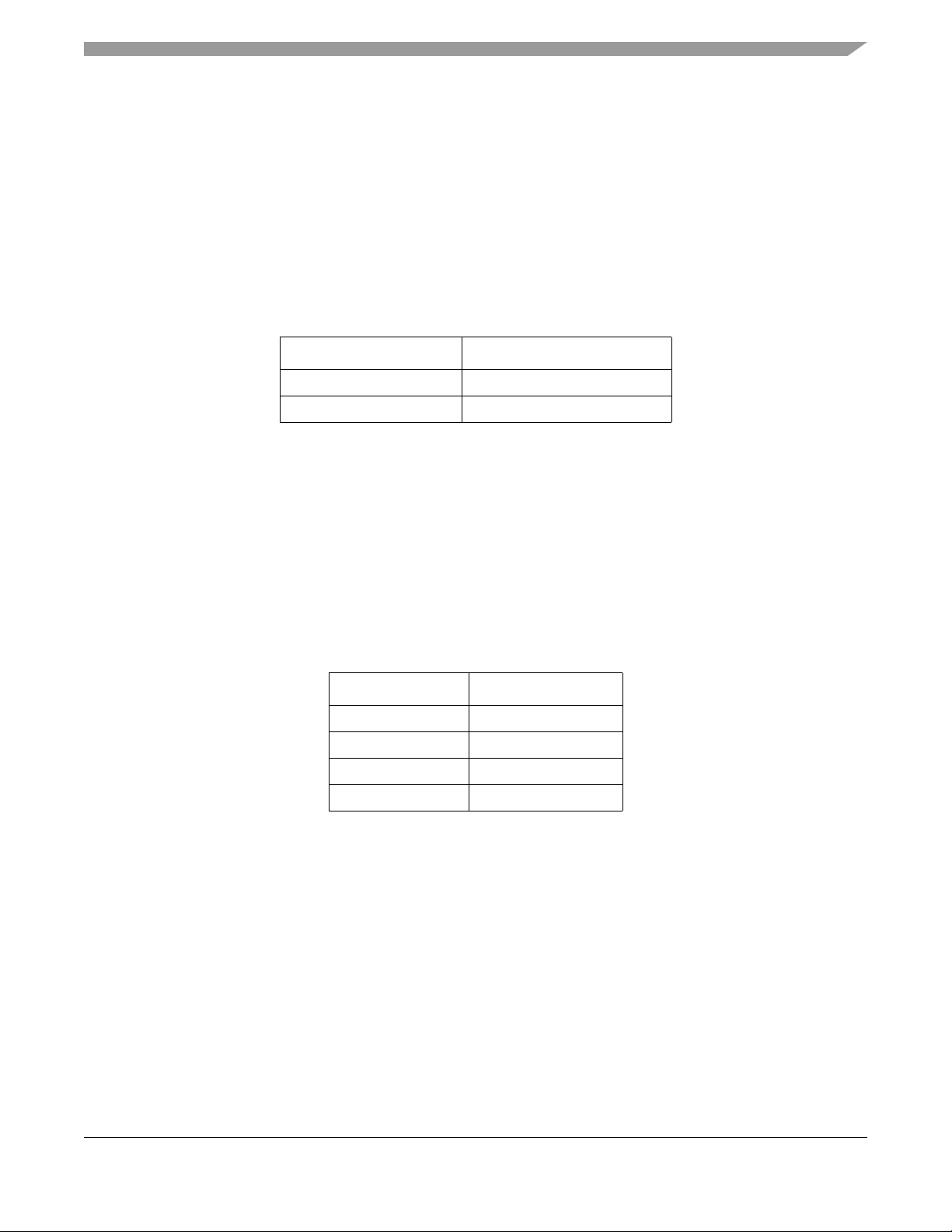
Table 2-1. Accepted voltage ranges
Voltag e M o d e Voltag e r a n ge
Nominal 7.0V to 18.0V
Over voltage 18.0V to 21.0V
Nominal voltage mode — Is when the board operates normally without any risk of damage. All the devices
operate according to their specification.
Over voltage mode — Is a voltage level where the power bus “battery switch” needs to be turned off by
the microcontroller and by setting low the pin PC13. The MCU can continuously sense the battery voltage.
When the voltage range is again nominal it is safe to turn on the battery switch.
The EVB includes a set of power buses that correctly distribute power to all the devices on the board.
Table 2-2 shows the different buses and the jumpers that enable and disable them.
MPC5606S-DEMO-V2 User Guide, Rev. 0
Freescale Semiconductor 3
Page 4
Video
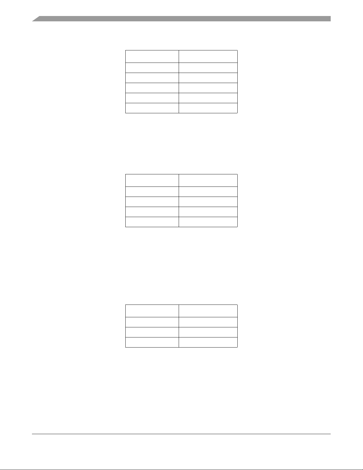
Table 2- 2. Po w e r b u s es
Power Bus Jumper Comments
5V_MCU J60 5V to certain power pins in the MCU.
3_MCU J62 3.3V to certain power pins in the MCU.
5V_LED J54 5V to the LEDs in the board.
Battery Switch J65 Battery power branch without any
regulation
3V_MEM J57 3.3V to the serial flash memories installed.
5V_Audio J58 5V to the audio circuit.
3V3_LCD J61 3.3V digital power to the TFT display
5V_LCD J66 5V analog power to the TFT display
The MCU requires both 5 V and 3.3 V because it is connected to the TFT display logic which is 3.3V. The
stepper motor module requires 5 V. Always install both J60 and J62 when using the MCU.
The 5V_Audio and 3V3_LCD require the battery switch J65 to be enabled in order to work.
The 5V_LCD requires that pin PC12 be set on high to turn on the voltage branch.
3Video
The MPC5606S has the capability to drive TFT Displays directly using the DCU module interface.
3.1 Display
The display is powered by three buses: 3.3 V, 5 V, and the backlight voltage which is 28 V. The
specification of the display requires the power to be supplied in the following order:
1. 5 Volts for analog power (enabled with pin PC12)
2. 3.3 V for digital power (enabled with the battery switch bus with pin PC13)
3. Backlight (not mandatory, enable backlight circuit using pin PG12)
The display also includes a Resistive Touch Interface connected on J71 through the ADC channels from
the MCU.
The MPC5606S-DEMO-V2 provides a port for a custom adapter board for different display connectivity,
that is a 38 pin MICTOR on J68 with all the RGB, clocks, power, and touch interface signals.
For more details about the specification of the display read the LQ043T1DG01 datasheet.
3.2 Backlight Circuitry
The MPC5606S-DEMO-V2 has a Freescale MC34845 which is an analog device to drive LED strings. In
this case, the display included has a 9 LED string for the backlight. The circuit is designed to be supplied
from 7 V to 18 V and provide a stable 20 mA current to either eight or nine LEDs in a string.
MPC5606S-DEMO-V2 User Guide, Rev. 0
Freescale Semiconductor4
Page 5
Input and Output
The MC34845 can handle up to six strings. The anodes and cathodes can be accessed from J67. When
building an adapter to drive a different kind of display requiring more LED strings, J67 can be accessed
for that functionality.
The MC34845 is controlled using the MPC5606S MCU as shown in the table below:
Table 3-3. Control signals for the MC34845
Signal Functionality
Battery Switch
(PC13)
PWM_WAKE_BACKLIGHT
(PG12)
Provides power to the chip, must be
turned off when the system is not in
nominal voltage
PWM for controlling the intensity of the
backlight
The PWM frequency has to be below 100 KHz but preferably above 20 KHz to avoid an audible vibration
from the components. If dimming is not needed then pin PG12 can be set to high and to low to turn on and
off the backlight.
For more details refer to the MC34845 datasheet.
3.3 Parallel Data Input (PDI)
The MPC5606S can receive digital video as input. The J50 connector is provided matching signals to the
J72 connector. The J72 is an output port to the display. This allows performing simple interface testing by
connecting the output of one MPC5606S-DEMO-V2 board (J72) into another MPC5606S-DEMO-V2
board (J50).
It is possible to provide power to the J50 connector by setting jumpers on the J52 and J53. Never set the
jumpers if the other board already has them installed. They can only act as power sources but not as power
sinks.
4 Input and Output
The MPC5606S-DEMO-V2 provides some basic controls for interfacing, switch buttons, LEDs, and a two
row pin header with the remaining signals of the unused modules from the microcontroller.
There are five general input switch buttons and one reset button as shown in Table 4–4.
Table 4-4. Switch buttons
Name MCU PIN
DOWN (SW5) PF8
RIGHT (SW4) PF3
LEFT (SW3) PF9
TOP (SW2) PF4
ENTER (SW6) PF1
Reset (SW7) RESET
MPC5606S-DEMO-V2 User Guide, Rev. 0
Freescale Semiconductor 5
Page 6

Input and Output
The board has three LEDs which are powered with the 5 V_LED bus. The signals driving the LEDs are in
the following table.
Table 4-5. LEDs signal connections
Name MCU PIN/signal
LED1 (red) PK10
LED2 (red) PK11
LED3 (green) GND
The connector J51 is a two-row standard 100 mm pin header where all the unused pins from the
microcontroller are routed to. The following table shows the pin assignation of the J51 connector.
Table 4-6. Connector J51 pin assignment
Pin Number MCU Signal Pin Number MCU Signal
1 PD0 2 PD1
3 PD2 4 PD3
5 PD4 6 PD5
7 PD6 8 PD7
9PD810PD9
11 PD10 12 PD11
13 PD12 14 PD13
15 PD14 16 PD15
17 PE0 18 PE1
19 PE2 20 PE3
21 PE4 22 PE5
23 PE6 24 PE7
25 NC 26 NC
27 PB4 28 PB6
29 PB10 30 PB11
31 NC 32 PC11
33 NC 34 NC
35 PC14 36 NC
37 PC15 38 PF2
39PF040PF6
41PF542NC
43PF744PH5
45 PJ14 46 PJ15
47 PK0 48 NC
MPC5606S-DEMO-V2 User Guide, Rev. 0
Freescale Semiconductor6
Page 7
Memory
It is then possible to use the stepper motor control functionality by getting the signals from the J51
connector.
5Memory
The MPC5606S-DEMO-V2 has an external serial flash memory that connects to the microcontroller using
a quad serial peripheral interface (QSPI) at high clock speeds (max 52 MHz). By using a multiplexer that
selects between the memories using a GPIO pin from the microcontroller it is possible to have two QSPI
memories installed on the board and to be able to access independently.
Table 5-7. QSPI select multiplexer
Signal Device
PC2 logic 1 U51 (S25FL064P0XMFV001)
PC2 logic 0 U50 (Not populated)
6 Communications
The MPC5606S-DEMO-V2 implements CAN, LIN, and TTL-UART physical interfaces.
6.1 CAN
The EVB uses the Freescale MC33902 high speed (from 40 kbps to 1 Mbps) CAN physical interface
transceiver that can be directly connected to the battery line. The J64 male DB-9 connector provides the
physical connectivity. The table below shows the connector pin mapping.
Table 6-8. J64 CAN connector pin mapping
Signal Pins
CANH 7
CANL 2
GND 6, 3, 5, M1, M2
NC 9, 4, 8, 1
The CAN bus termination is specified to be 60 ohms. If the MPC5606S-DEMO-V2 is going to be used as
the node with the 60 ohm CAN bus termination on J63 shunt pins 1 and 2 and shunt pins 3 and 4.
The CAN transceiver is connected to the MCU via the pins shown in Table 6-9.
MPC5606S-DEMO-V2 User Guide, Rev. 0
Freescale Semiconductor 7
Page 8
Communications
Table 6-9. MC33902 pin connection to the MCU
MC33902 MCU pins
TXD PB0
RXD PB1
NERR PB7
EN PB8
STBY PB9
6.2 LIN
The physical LIN interface for the MPC5606S-DEMO-V2 is implemented with a Freescale MC33661 LIN
transceiver . The physical connectivity is provided by a four slot mini-fit Molex connector . The table below
shows the connections on the J56 connector.
Table 6-10. J56 LIN connector pin mapping
Signal Pins
LIN Power 3
GND 1
LIN signal 4
NC 2
Providing or receiving power through a LIN cable is optional with the configuration jumper J59. Be careful
when configuring:
Close J59 1 and 3 to either provide or receive power. If receiving power, the power input at J69
must be disconnected.
Close J59 2 and 4 for Master mode. When it is open the device works as a slave.
Connections from the MC33661 to the MCU are as follows:
Table 6-11. MC33661 pin connection to MCU
MC33902 MCU pins
TXD PB2
RXD PB3
EN PC8
MPC5606S-DEMO-V2 User Guide, Rev. 0
Freescale Semiconductor8
Page 9

Debug
6.3 UART
UART connectivity is provided through JP50 directly from the microcontroller at the 5 V level. The pin
connections on the JP50 are as follows:
Table 6-12. JP50 UART pin mapping
Signal JP50 pin MCU pins
TXD 5 PB13
RXD 4 PB12
CTS 2 PC0
RTS 6 PC1
GND 1 N/A
NC 3 N/A
7Debug
The MPC5606S-DEMO-V2 supports both the JTAG and Nexus for application development and debug
for the MPC5606S.
The JTAG connector is located in the back (bottom layer) of the board at J55. Be careful with the pin
numbering because connecting it wrongly may cause damage to the board (J55 Pin 1 must match Pin 1
from the debugging tool). The Nexus port J1 is located in front with a MICTOR 38 connector.
8 Sound
The MPC5606S-DEMO-V2 provides a loud-speaker with an amplifier that allows to generate sounds with
the microcontroller.
The potentiometer R10 allows to control the gain in the amplifier. The input sound signal comes from
MCU pin PC10. The audio amplifier is fed with a separate regulator because the current consumption of
the circuit on some cases can be high. The circuit can deliver up to 1 W of power to the loud-speaker.
9 Initialization Code
The hardware architecture on the MPC5606S-DEMO-V2 allows independent power on different modules
of the board. The following code listing provides the C code necessary to power the peripherals included
on the board.
MPC5606S-DEMO-V2 User Guide, Rev. 0
Freescale Semiconductor 9
Page 10

Revision History
Code List 1—Initialization code:
// Init of Ext. peripheral on MPC5606S-DEMO-V2
// Set data output pins to 0 first
SIU.GPDO[PC13].R = 0;
SIU.GPDO[PC12].R = 0;
SIU.GPDO[PG12].R = 0;
// Configure pins as outputs
SIU.PCR[PC13].R = 0x0200;
SIU.PCR[PC12].R = 0x0200;
SIU.PCR[PG12].R = 0x0200;
SIU.GPDO[PC13].R = 1; // Enable battery switch branch
SIU.GPDO[PC12].R = 1; // Enable 5V lcd analog supply
SIU.GPDO[PG12].R = 1; // Enable Backlight
// QSPI Memory Mux
SIU.GPDO[PC2].R = 0; // 0 for U51, (set to 1 for U50)
SIU.PCR[PC2].R = 0x0200; // EN QSPI Mux select pin
// CAN transceiver activation
SIU.GPDO[PB8].R = 1; // Enable CAN_EN signal
SIU.PCR[PB8].R = 0x0200; // Set CAN_EN pin as output
SIU.GPDO[PB9].R = 1; // Enable CAN_STBY signal */
SIU.PCR[PB9].R = 0x0200; // Set CAN_STBY pin as output
// LIN transceiver activation
SIU.GPDO[PC8].R = 1; // Enable LIN_ENABLE signal
SIU.PCR[PC8].R = 0x0200; // Set LIN_ENABLE pin as output
10 Revision History
Revision
Number
0 October 2010 Initial Version
Revision Date Description of Changes
Added MPC5606S information on
• overview section
• initialization code
•index
MPC5606S-DEMO-V2 User Guide, Rev. 0
Freescale Semiconductor10
Page 11

Revision History
MPC5606S-DEMO-V2 User Guide, Rev. 0
Freescale Semiconductor 11
Page 12

How to Reach Us:
Home Page:
www.freescale.com
Web Support:
http://www.freescale.com/support
USA/Europe or Locations Not Listed:
Freescale Semiconductor, Inc.
Technical Information Center, EL516
2100 East Elliot Road
Tempe, Arizona 85284
+1-800-521-6274 or +1-480-768-2130
www.freescale.com/support
Europe, Middle East, and Africa:
Freescale Halbleiter Deutschland GmbH
Technical Information Center
Schatzbogen 7
81829 Muenchen, Germany
+44 1296 380 456 (English)
+46 8 52200080 (English)
+49 89 92103 559 (German)
+33 1 69 35 48 48 (French)
www.freescale.com/support
Japan:
Freescale Semiconductor Japan Ltd.
Headquarters
ARCO Tower 15F
1-8-1, Shimo-Meguro, Meguro-ku,
Tokyo 153-0064
Japan
0120 191014 or +81 3 5437 9125
support.japan@freescale.com
Asia/Pacific:
Freescale Semiconductor China Ltd.
Exchange Building 23F
No. 118 Jianguo Road
Chaoyang District
Beijing 100022
China
+86 10 5879 8000
support.asia@freescale.com
For Literature Requests Only:
Freescale Semiconductor Literature Distribution Center
1-800-441-2447 or 303-675-2140
Fax: 303-675-2150
LDCForFreescaleSemiconductor@hibbertgroup.com
Information in this document is provided solely to enable system and software
implementers to use Freescale Semiconductor products. There are no express or
implied copyright licenses granted hereunder to design or fabricate any integrated
circuits or integrated circuits based on the information in this document.
Freescale Semiconductor reserves the right to make changes without further notice to
any products herein. Freescale Semiconductor makes no warranty, representation or
guarantee regarding the suitability of its products for any particular purpose, nor does
Freescale Semiconductor assume any liability arising out of the application or use of any
product or circuit, and specifically disclaims any and all liability, including without
limitation consequential or incidental damages. “Typical” parameters that may be
provided in Freescale Semiconductor data sheets and/or specifications can and do vary
in different applications and actual performance may vary over time. All operating
parameters, including “Typicals”, must be validated for each customer application by
customer’s technical experts. Freescale Semiconductor does not convey any license
under its patent rights nor the rights of others. Freescale Semiconductor products are
not designed, intended, or authorized for use as components in systems intended for
surgical implant into the body, or other applications intended to support or sustain life,
or for any other application in which the failure of the Freescale Semiconductor product
could create a situation where personal injury or death may occur. Should Buyer
purchase or use Freescale Semiconductor products for any such unintended or
unauthorized application, Buyer shall indemnify and hold Freescale Semiconductor and
its officers, employees, subsidiaries, affiliates, and distributors harmless against all
claims, costs, damages, and expenses, and reasonable attorney fees arising out of,
directly or indirectly, any claim of personal injury or death associated with such
unintended or unauthorized use, even if such claim alleges that Freescale
Semiconductor was negligent regarding the design or manufacture of the part.
RoHS-compliant and/or Pb-free versions of Freescale products have the functionality
and electrical characteristics as their non-RoHS-compliant and/or non-Pb-free
counterparts. For further information, see http://www.freescale.com or contact your
Freescale sales representative.
For information on Freescale’s Environmental Products program, go to
http://www.freescale.com/epp.
Freescale™ and the Freescale logo are trademarks of Freescale Semiconductor, Inc.
All other product or service names are the property of their respective owners.
© Freescale Semiconductor, Inc. 2010. All rights reserved.
Document Number: MPC5606SDEMOUG
Rev. 0
10/2010
 Loading...