

Page 1

Freescale
User’s Guide
Document Number: MPC5604PUG
Rev. 0, 07/2012
MPC5604P Controller Board
User’s Guide
by: Petr Konvicny
Automotive and Industrial Solutions Group
1 About This Book
This document describes the design of MPC5604P
Controller Board, which is targeted for rapid
development of motor control applications.
To locate any published updates for this document, refer
to the world-wide web at: http://www.freescale.com/.
2 Introduction
Freescale MPC5604P Controller Board is a controller
board integrated to Freescale embedded motion-control
series of development tools. It is supplied with universal
interface interconnecting with, among others, one of the
embedded motion-power stages or evaluation boards,
providing a ready-made software-development platform
for a various electrical motors, DC converters.
The MPC5604P Controller Board is an
evaluation-module type of board which includes an
MPC5604P device, a various position sensing interfaces,
Contents
1 About This Book . . . . . . . . . . . . . . . . . . . . . . . . . . . . . . . . . . . . . . . 1
2 Introduction . . . . . . . . . . . . . . . . . . . . . . . . . . . . . . . . . . . . . . . . . . . 1
2.1 Features. . . . . . . . . . . . . . . . . . . . . . . . . . . . . . . . . . . . . . . . . 2
2.2 MPC5604P Controller Board Architecture . . . . . . . . . . . . . . . 3
2.3 Board Jumper Configuration . . . . . . . . . . . . . . . . . . . . . . . . . 4
2.4 Board LEDs . . . . . . . . . . . . . . . . . . . . . . . . . . . . . . . . . . . . . . 7
3 Interface Description . . . . . . . . . . . . . . . . . . . . . . . . . . . . . . . . . . . . 8
3.1 Power Supply J100 . . . . . . . . . . . . . . . . . . . . . . . . . . . . . . . . 8
3.2 UNI3 Interface J300 . . . . . . . . . . . . . . . . . . . . . . . . . . . . . . . . 9
3.3 MC33937A Interface J302 . . . . . . . . . . . . . . . . . . . . . . . . . . 11
3.4 Resolver Connector J207 . . . . . . . . . . . . . . . . . . . . . . . . . . 11
3.5 Encoder/Hall Connector J500 and J501 . . . . . . . . . . . . . . . 12
3.6 LIN Connector J101 . . . . . . . . . . . . . . . . . . . . . . . . . . . . . . . 13
3.7 CAN Connector J103 . . . . . . . . . . . . . . . . . . . . . . . . . . . . . . 14
3.8 USB Connector J311 . . . . . . . . . . . . . . . . . . . . . . . . . . . . . . 15
3.9 Header J10 and J15. . . . . . . . . . . . . . . . . . . . . . . . . . . . . . . 15
3.10 Header J4, J7, and J9 . . . . . . . . . . . . . . . . . . . . . . . . . . . . . 16
3.11 Header J3 . . . . . . . . . . . . . . . . . . . . . . . . . . . . . . . . . . . . . . 18
4 Design Consideration . . . . . . . . . . . . . . . . . . . . . . . . . . . . . . . . . . 19
4.1 MPC5604P Features . . . . . . . . . . . . . . . . . . . . . . . . . . . . . . 19
4.2 Clock Source . . . . . . . . . . . . . . . . . . . . . . . . . . . . . . . . . . . . 20
4.3 UNI3 Interfaces and External Fault Management . . . . . . . . 21
4.4 Encoder/Hall Sensor Interface . . . . . . . . . . . . . . . . . . . . . . . 22
4.5 Resolver and SinCos Sensor Interface . . . . . . . . . . . . . . . . 23
4.6 Analog Signal Sensing. . . . . . . . . . . . . . . . . . . . . . . . . . . . . 26
4.7 Power Supplies and Voltage Reference . . . . . . . . . . . . . . . 26
4.8 UNI-3 PFC-PWM Signal (Power Factor Correction) . . . . . . 27
4.9 UNI-3 Brake Signal . . . . . . . . . . . . . . . . . . . . . . . . . . . . . . . 27
4.10 CAN Bus . . . . . . . . . . . . . . . . . . . . . . . . . . . . . . . . . . . . . . . 27
4.11 FlexRAY Interface . . . . . . . . . . . . . . . . . . . . . . . . . . . . . . . . 27
5 Electrical Characteristics . . . . . . . . . . . . . . . . . . . . . . . . . . . . . . . . 28
6 Board Set-Up Guide . . . . . . . . . . . . . . . . . . . . . . . . . . . . . . . . . . . 28
7 MPC5604P Controller Board Schematics . . . . . . . . . . . . . . . . . . . 29
8 References . . . . . . . . . . . . . . . . . . . . . . . . . . . . . . . . . . . . . . . . . . 30
© Freescale, Inc., 2012. All rights reserved.
Page 2

Introduction
communications options, digital and analog power supplies, and peripheral expansion connectors. The
expansion connectors are intended for signal monitoring and user expandability. Test pads are provided for
monitoring critical signals and voltage levels.
The MPC5604P Controller Board facilitates the evaluation of various features present in the MPC5604P.
It can be used to develop real-time software and hardware products based on MPC5604P in TQFP144
package. It provides the features necessary for the user to write and debug software, demonstrate the
functionality of that software, and to interface with the customer’s application specific device(s). The
MPC5604P Controller Board is flexible enough to allow the users to fully exploit the MPC5604P features
to optimize the performance of their product, as shown in Figure 1.
2.1 Features
The MPC5604P Controller Board facilitates the evaluation of various features present in the MPC5604P.
Following are the board features:
• MPC5604P microcontroller, TQFP144 package
• JTAG/NEXUS interfaces for MCU code download and debugging
• System-basis chip MCZ33905D
• Motor control interface:
— UNI-3
— MC33937A predriver
— Resolver
— two Encoder/Hall sensors
• Connectivity interface:
—LIN
—CAN
—FlexRay
— USB interface
• LEDs:
— Power-supply indicators
— PWM control signals
— Faults monitoring
— SBC safe mode
— User application
• Two push buttons and switch for application control
• MCU pins accessible via pin headers
• Power plug 2.1mm connector.
MPC5604P Controller Board User’s Guide, Rev. 0
Freescale2
Page 3

Introduction
2.2 MPC5604P Controller Board Architecture
The MPC5604P Controller Board is flexible enough to allow the user to fully exploit the MPC5604P
features to optimize a performance of their product. Its basic building blocks are depicted in Figure 1. The
block color differentiates a block function.
• Blue - MCU and application software download and the debug interface
• Green - Motor control related hardware
• Red - Board power supply and connectivity
• Violet - Application control
Figure 1. MPC5604P Controller Board Block Diagram
The board can be supplied by VBAT voltage in the range of 8V to 18V. The MC33905 provides two
independent voltage sources, one for supplying MCU and second for auxiliary logic. Both sources
provides either 3.3V or 5V, depending on the assembled SBC version.
The UNI-3 expansion interface enables MCU to direct control of the electrical motor or DC/DC
converters.
The Fault logic triggers several important system faults as described in a particular chapter. The circuitry
behavior depends on the selected configuration. For more info, see Section 3, “Interface Description.
The user can control the application using the rotary switch, USB interface (RS232), CAN and LIN buses.
The JTAG/NEXUS interfaces is present on-board to enable download and debugging of MCU code.
MPC5604P Controller Board User’s Guide, Rev. 0
Freescale 3
Page 4

Introduction
For the on-board block location, see Figure 2.
Figure 2. MPC5604P Controller Board Block Location
2.3 Board Jumper Configuration
See Table 1 and Figure 3 for proper jumper configuration.
Table 1. MPC5604P Controller Board Jumper Options
# Selector Function Connections
JP1, JP2 CAN Terminate CAN bus node. closed
JP104 MC33905
debug mode
JP105 MC33905
save mode
JP200 Resolver Enable Resolver reference input
J203 Resolver REFSIN input Positive input for SIN OPAM
Enter SBC driver MC33905
to debug mode.
Enter SBC driver MC33905
to safe mode.
signal from MCU disabled.
Resolver reference input
signal from MCU enabled
is DC offset voltage set up by
trimmer R209.
Positive input for SIN OPAM
is REFSIN input of resolver.
closed
closed
open
closed
1-2
2-3
MPC5604P Controller Board User’s Guide, Rev. 0
Freescale4
Page 5

Table 1. MPC5604P Controller Board Jumper Options
# Selector Function Connections
Introduction
J204 Resolver COS input Positive input for COS
OPAM is DC offset voltage
set up by trimmer R209.
Positive input for COS
OPAM is REFCOS input of
resolver.
J205 Phase A
digital signal
Resolver Phase A signal is
connected to GPIO F[13].
SIN/COS Phase A signal is
connected to GPIO F[13].
J206 Phase B
digital signal
Resolver Phase A signal is
connected to GPIO A[5].
SIN/COS Phase A signal is
connected to GPIO A[5].
J2 Resolver
input signal
Resolver reference signal is
generated by GPIO C[11].
Resolver reference signal is
generated by GPIO C[12].
J301 FAULT1 selection UNI-3 Phase A over-current
signal is connected to
FAULT1 input G[9].
UNI-3 DC-bus over-current
signal is connected to
FAULT1 input G[9].
J312 BOOT selection MPC5604P boot from
internal Flash.
J500 Encoder 0 Phase A Encoder0 JP500 pin three
PHASE A input signal is
connected to GPIO A[0].
UNI-3 BEMFZCA input
signal is connected to GPIO
A[0].
J501 Encoder 0 Phase B Encoder0 JP500 pin four
PHASE B input signal is
connected to GPIO A[1].
UNI-3 BEMFZCB input
signal is connected to GPIO
A[1].
J502 Encoder 0 Index Encoder0 JP500 pin five
INDEX input signal is
connected to GPIO A[2].
UNI-3 BEMFZCC input
signal is connected to GPIO
A[2].
1-2
2-3
1-2
2-3
1-2
2-3
2-3
1-2
1-2
2-3
closed
1-2
2-3
1-2
2-3
1-2
2-3
MPC5604P Controller Board User’s Guide, Rev. 0
Freescale 5
Page 6

Introduction
Table 1. MPC5604P Controller Board Jumper Options
# Selector Function Connections
J503 Encoder 0 Home Encoder0 JP500 pin six
HOME input signal is
connected to GPIO A[3].
DC BUS Voltage DC BSUS Voltage signal
from UNI-3 is connected to
GPIO B[13], ADC 1 input
zero.
DC BUS Current DC BUS Current signal from
UNI-3 is connected to GPIO
B[15], ADC 1 input two.
Analog input 11 UNI-3 Phase A current is
connected to GPIO B[9],
ADC 0/1 input 11.
UNI-3 Phase A Back-EMF
Voltage is connected to
GPIO B[9]m ADC 0/1 input
11.
Analog input 12 UNI-3 Phase B current is
connected to GPIO B[10],
ADC 0/1 input 12
UNI-3 Phase B Back-EMF
Voltage is connected to
GPIO B[10]m ADC 0/1 input
12.
Analog input 13 UNI-3 Phase C current is
connected to GPIO B[11],
ADC 0/1 input 13.
UNI-3 Phase C Back-EMF
Voltage is connected to
GPIO B[11]m ADC 0/1 input
13.
closed
R315 populated
R316 populated
R318 populated
R320 populated
R322 populated
R324 populated
R325 populated
R326 populated
TEMP UNI-3 Temperature signal is
SERIAL UNI-3 Serial signal is
MPC5604P Controller Board User’s Guide, Rev. 0
R328 populated
connected to ADC0 input
zero.
R330 populated
connected to GPIO D[5].
Freescale6
Page 7

Table 1. MPC5604P Controller Board Jumper Options
# Selector Function Connections
Introduction
BRAKE UNI-3 Brake output signal is
connected to GPIO C[3].
PFC UNI-3 PFC output signal is
connected to GPIO G[6]
(PWMA3).
PFC_EN UNI-3 PFC Enable signal is
connected to GPIO G[7]
(PWMB3).
PFC_ZC UNI-3 PFC zero current
signal is connected to GPIO
G[5] (PWMX3).
R333 populated
R334 populated
R335 populated
R336 populated
Figure 3. MPC5604P Controller Board Jumper Position
2.4 Board LEDs
The Table 2 displays the on-board LEDs. For on-board LED locations, see Figure 2.
MPC5604P Controller Board User’s Guide, Rev. 0
Freescale 7
Page 8

Interface Description
Table 2. On-board LEDs
LED Signal Name Description
D114 /SAFE MCZ33905 safe pin state
(ON - SBC in safe mode)
D14 +3.3Vdc + 3.3V AUX power supply
D1 PWM0 A0 Motor 1 Phase A bottom
switch signal
D2 PWM0 B0 Motor 1 Phase B bottom
switch signal
D3 PWM0 A1 Motor 1 Phase C bottom
switch signal
D4 PWM0 B1 Motor 1 Phase C top switch
signal
D5 PWM0 A2 Motor 1 Phase B top switch
signal
D6 PWM0 B2 Motor 1 Phase A top switch
signal
D7 FAULTB0 Motor 1 FAULTB0 signal
D8 FAULTB1 Motor 1 FAULTB1 signal
D9 FAULTB2 Motor 1 FAULTB2 signal
D10 FAULTB3 Motor 1 FAULTB3 signal
D11 A12 User LED 1
D12 PHASEA0 Encoder 1 input A signal
D15 PHASEB0 Encoder 1 input B signal
D17 INDEX0 Encoder 1 input INDEX
signal
D13 PWM0 A3 PWM module 0, A3 output
D16 PWM0 B3 PWM module 0, B3 output
D18 A13 User LED 1
3 Interface Description
The following chapters summarize the on-board connectors and headers pin-outs, signal meanings and
MCU pins assignments.
3.1 Power Supply J100
The MPC5604P Controller Board can be supplied either by using the 2.1 mm DC power plug J100 or the
UNI-3 connector (J300, pin 19).
MPC5604P Controller Board User’s Guide, Rev. 0
Freescale8
Page 9

Interface Description
The controller board is powered from two independent voltage regulators which provides 5V for a
auxiliary logic and 5V for MCU and debugger logic. Both voltages are generated by the MC33905 SBC
integrated circuit. Proper operation is monitored by LED D114 for the AUX 3.3V line, see Table 2.
The board is designed to operate in the voltage range from 8V to 18V. The board is protected against a
reverse battery.
3.2 UNI3 Interface J300
The UNI-3 interface (connector J300) defines the interface between the MPC5604P Controller Board and
a 3 phase electrical motor power stages.
The list of UNI-3 signals follows:
• Control signals:
— PWM phase A, B, C top and bottom switches control
— Brake signal control
— Power Factor Correction (PFC)
• Monitor signals
— DC-bus voltage
— DC-bus current
— Phase A, B, C current
— Zero-cross signals
— Back-EMF phase A, B, C
— Temperature monitoring
• Power Supply 12V
• Serial line - a bidirectional communication line between the Controller Board and Power Stage
The Table 3 defines the UNI-3 pin-out and pin assignment to the MCU.
Table 3. Motor 1 - UNI-3 Signal Description
Interface Pin Signal Name MCU Signal Description Direction
1 PWM_AT PWM_A0 Phase A top switch
control (H -> Turn OFF)
3 PWM_AB PWM_B0 Phase A bottom switch
control (H -> Turn ON)
5 PWM_BT PWM_A1 Phase B top switch
control (H -> Turn OFF)
7 PWM_BB PWM_B1 Phase B bottom switch
control (H -> Turn ON)
Digital output
Digital output
Digital output
Digital output
9 PWM_CT PWM_A2 Phase C top switch
11 PWM_CB PWM_B2 Phase C bottom switch
MPC5604P Controller Board User’s Guide, Rev. 0
Freescale 9
Digital output
control (H -> Turn OFF)
Digital output
control (H -> Turn ON)
Page 10

Interface Description
Table 3. Motor 1 - UNI-3 Signal Description
Interface Pin Signal Name MCU Signal Description Direction
2,4,6,8,10 Shield — PWM signals shield
—
(grounded on the power
stage side only)
12,13 GND_D — Digital power supply
—
ground
14,15 +5V DC — +5V digital power supply —
17,18 AGND — Analog power supply
—
ground
19 +12/+15V DC — Analog power supply —
16,20,27,28,37 NC — Not connected —
21 V
BUS B[13] DC-bus voltage
DC
Analog input
sensing, 0V – 3.3V,
ADC1 channel 0
22 I
BUS B[15] DC-bus current sensing,
DC
Analog input
0V – 3.3V, ADC1
channel 2
23 I
A
B[9] Phase A current
Analog input
sensing, 0V – 3.3V,
ADCx channel 11
24 I
B
B[10] Phase B current
Analog input
sensing, 0V – 3.3V,
ADCx channel 12
25 I
C
B[11] Phase C current
Analog input
sensing, 0V – 3.3V,
ADCx channel 13
26 TEMP B[7] Analog temperature 0V
Analog input
– 3.3V, ADC0 channel 0
29 BRAKE_CONT EIRQ#22 DC-bus brake control Digital output
30 SERIAL D[5] Serial interface Digital bi-directional
31 PFC PWM_A3 Power factor correction
Digital output
PWM
32 PFCEN PWM_B3 Power factor correction
Digital output
enable
33 PFCZC PWM_X3 Power factor correction
Digital input
Zero-cross
34 ZCA D[9] or A[0] Phase A Back-EMF
Digital input
zero crossing
35 ZCB D[12] or A[1] Phase B Back-EMF
Digital input
zero crossing
MPC5604P Controller Board User’s Guide, Rev. 0
Freescale10
Page 11

Interface Description
Table 3. Motor 1 - UNI-3 Signal Description
Interface Pin Signal Name MCU Signal Description Direction
36 ZCC G[2] or A[2] Phase C Back-EMF
zero crossing
38 Back-EMF_A B[9] Phase A Back-EMF
voltage sensing
39 Back-EMF_B B[10] Phase B Back-EMF
voltage sensing
40 Back-EMF_C B[11] Phase C Back-EMF
voltage sensing
Digital input
Analog input
Analog input
Analog input
3.3 MC33937A Interface J302
When using a Freescale 3-phase power stages, the electrical inverter switches are controlled by the
MC33937A pre-driver. The device behavior is configured by this interface, see Table 4.
Table 4. Motor 1 - MC33937A Signal Description
Interface Pin Signal Name MCU Signal Description Direction
1 NC — Not connected. —
2 NC — Not connected. —
3 33937_EN G[0] Motor 1 device-enable
output.
4 33937_OC C[8] Over-current input. Digital input
Digital output
5 33937_/RST C[10] Reset output. Active in
low.
6 33937_INT C[9] Interrupt pin. Digital input
7 33937_SOUT DSPI3_SIN Input data from
MC33937 SPI port.
Tri-state until CS
becomes low.
8 33937_SCK DSPI3_SCK Clock for SPI port.
Output.
9 33937_CS DSPI3_/CS0 Chip-select 0 output. It
frames SPI command
and enables SPI port.
10 33937_SIN DSPI3_SOUT Output data for
MC33937 SPI port.
Clocked on the falling
edge of SCLK, MSB
first.
Digital output
Digital input
Digital output
Digital output
Digital output
3.4 Resolver Connector J207
The controller board is able to calculate motor rotor position from resolver or SIN/COS sensor. They are
connected to the board through connectors J207, Tab le 5 shows pin description.
MPC5604P Controller Board User’s Guide, Rev. 0
Freescale 11
Page 12

Interface Description
Table 5. Resolver Signal Description
Interface Pin Signal Name MCU Signal Description Direction
1 RES_GEN Positive sinusoidal
reference signal for
resolver
Signal output range
from 0 V up to +12 V
2 GNDP Ground for reference
signal
3 SIN SIN input signal Differential analog input
4 REFSIN SIN reference input
signal
5 COS COS input signal Differential analog input
6 REFCOS COS reference input
signal
7 GNDA Analog ground —
8 +5VA +5V Analog Power
supply
Output
—
Differential analog input
Differential analog input
—
3.5 Encoder/Hall Connector J500 and J501
The motor rotor position can be transformed from encoder or Hall rotor position sensor. They can be
connected to the board through connector J500 and J501. For proper signal connection, see Table 6.
Table 6. Encoder/Hall Signal Description
Interface Pin Signal Name MCU Port Description Direction
1 +5Vdc — +5V sensor supply
voltage
2GND— Ground—
3 ENC1_PhaseA /
HALL0
ENC2_PhaseA /
HALL0
4 ENC1_PhaseB /
HALL1
ENC2_PhaseB /
HALL1
5 ENC1_INDEX /
HALL2
ENC2_INDEX /
HALL2
6 ENC1_HOME A[3] Digital input signals
A[0]
C[13]
A[1]
C[14]
A[2]
F[12]
Digital input signal phase
A or Hall 0 input signal
Digital input signals
phase B or Hall 1 input
signal
Digital input signals
INDEX or Hall 2 input
signal
HOME
—
Digital input
Digital input
Digital input
Digital input
MPC5604P Controller Board User’s Guide, Rev. 0
Freescale12
Page 13

Interface Description
Table 7. J6 Header Signal Description
Interface Pin Signal Name MCU Port Description Direction
1 PHASEB0 A[1] Encoder 1 digital input signal
phase B.
2 PHASEA0 A[0] Encoder 1 digital input signal
phase A.
3 HOME0 A[3] Encoder 1 digital input signal
Home.
4 INDEX0 A[2] Encoder 1 digital input signal
Index.
5 ET0_4 C[11] eTimer0 channel 4
output/input
6 ET0_5 C[12] eTimer0 channel 5
output/input
7 +3.3Vdc — +3.3Vdc power supply —
8 GND — Ground —
Digital input
Digital input
Digital input
Digital input
Digital I/O
Digital I/O
Table 8. J8 Header Signal Description
Interface Pin Signal Name MCU Port Description Direction
1 PHASEB1 C[14] Encoder 2 digital input
signal phase B.
2 PHASEA1 C[13] Encoder 2 digital input
signal phase A.
3NC ———
4 INDEX1 F[12] Encoder 2 digital input
signal Index.
5 PHASE_A F[13] eTimer1 channel 4
output/input
Digital input
Digital input
Digital input
Digital I/O
6 PHASE_B A[5] eTimer1 channel 5
7 +3.3Vdc — +3.3Vdc power supply —
8 GND — Ground —
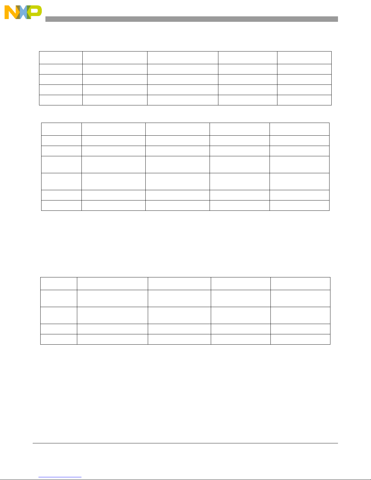
3.6 LIN Connector J101
The MC33905 LIN transceiver is used as an on-board LIN hardware interface. The LIN node can be
configured to either the Master or Slave mode, see Tab le 1.
A Table 9 shows the LIN connector pin-out and pin assignment to the MCU.
MPC5604P Controller Board User’s Guide, Rev. 0
Freescale 13
Digital I/O
output/input
Page 14
Interface Description
Table 9. LIN Signal Description
Interface Pin Signal Name MCU Signal Description Direction
1 GND — Ground —
2 VSUP — Power Supply —
3 GND — Ground —
4 LIN LIN1_RXD / LIN1_TXD LIN bus Digital bi-directional
Table 10. Header J14 Signal Description
Interface Pin Signal Name MCU Port Description Direction
1 GPIOA13 A[13] Digital input / output Digital I/O
2 GPIOA12 A[12] Digital input / output Digital I/O
3 LIN1_TXD F[14] LIN module 1 transmit
output
Digital output
4 LIN1_RXD F[15] LIN module 1 receive
input
5 GND — Ground —
6 +3.3Vdc — +3.3Vdc power supply —
Digital input
3.7 CAN Connector J103
The system basis chip MC33905 CAN transceiver is used as the CAN hardware interface. An on-board
jumpers JP1, JP2 enable node termination, impedance of 120R, see Table 1.
Table 11 shows the CAN connector pin-out and pin assignment to the MCU.
Table 11. CAN Signal Description
Interface Pin Signal Name MCU Signal Description Direction
1 CANH CAN0_RXD /
CAN0_TXD
2 CANL CAN0_RXD /
CAN0_TXD
3GND — Ground —
4 NC — Not connected —
CAN bus H Differential bidirectional
CAN bus L Differential bidirectional
MPC5604P Controller Board User’s Guide, Rev. 0
Freescale14
Page 15
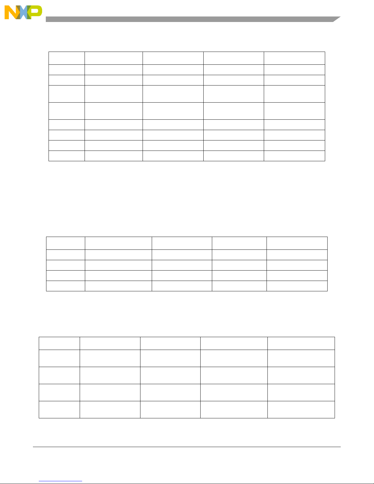
Interface Description
Table 12. Header J11 Signal Description
Interface Pin Signal Name MCU Port Description Direction
1 CAN0_RX_PHY
2 CAN0_TX_PHY
3 CAN0_RXD B[1] CAN module 0 receive
input
4 CAN0_TXD B[0] CAN module 0 receive
output
5 GND — Ground —
6 GND — Ground —
7 +5Vdc — +5Vdc power supply —
8 +3.3Vdc — +3.3Vdc power supply —
Digital input
Digital output
3.8 USB Connector J311
The USB line is used for board communication with the PC, when using for example, Freescale
FreeMASTER tool to control and visualize the user application.
The interface uses a A type connector and it is isolated from the board environment. See Table 13 for the
pin description and pin assignment to the MCU.
Table 13. USB Signal Description
Interface Pin Signal Name MCU Signal Description Direction
1 VBUS — USB Power Supply —
2 D- LIN0_RXD / LIN0_TXD Data- Dig. bidirectional
3 D+ LIN0_RXD / LIN0_TXD Data+ Dig. bidirectional
4 GNDB — USB Ground —
3.9 Header J10 and J15
Monitoring the PWM signals is possible using J10. The Table 14 summarizes the header pin-out.
Table 14. J10- Signal Description
Interface Pin Signal Name MCU Signal Description Direction
1 PWMA0 D[10] Motor 1 - Phase A top
switch control
2 PWMB0 D[11] Motor 1 - Phase A bottom
switch control
3 PWMA1 D[13] Motor 1 - Phase B top
switch control
4 PWMB1 D[14] Motor 1 - Phase B bottom
switch control
Digital output
Digital output
Digital output
Digital output
MPC5604P Controller Board User’s Guide, Rev. 0
Freescale 15
Page 16
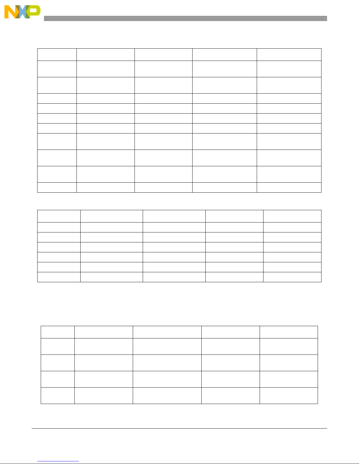
Interface Description
Table 14. J10- Signal Description
Interface Pin Signal Name MCU Signal Description Direction
5 PWMA2 G[3] Motor 1 - Phase C top
switch control
6 PWMB2 G[4] Motor 1 - Phase C bottom
switch control
7 FAULTB0 G[8] PWM module fault input 0 Digital input
8 FAULTB1 G[9] PWM module fault input 1 Digital input
9 FAULTB2 G[10] PWM module fault input 2 Digital input
10 FAULTB3 G[11] PWM module fault input 3 Digital input
11 PWM_X0 D[9] PWM module 0 auxiliary
PWM signal 0
12 PWM_X1 D[12] PWM module 0 auxiliary
PWM signal 1
13 PWM_X2 G[2] PWM module 0 auxiliary
PWM signal 2
14 GND — Ground —
Digital output
Digital output
Digital input/output
Digital input/output
Digital input/output
Table 15. J15 Signal Description
Interface Pin Signal Name MCU Port Description Direction
1 PWMA3 G[6] Digital input/output Digital I/O
2 PWMB3 G[7] Digital input/output Digital I/O
3 PWM_X3 G[4] Digital input/output Digital I/O
4 NCs — — —
5 +3.3Vdc — +3.3V voltage —
6 GND — Ground —
3.10 Header J4, J7, and J9
Headers J4, J6, and J7 allows monitoring the analog-to-digital converter signals, see Table 16.
Table 16. Header J4 Signal Description
Interface Pin Signal Name MCU Signal Description Direction
1 ADC0_AN0 B[7] ADC module 0 channel
0 input
2 ADC0_AN1 B[8] ADC module 0 channel
1 input
3 ADC0_AN2 C[1] ADC module 0 channel
2 input
4 ADC0_AN3 C[2] ADC module 0 channel
3 input
Analog input
Analog input
Analog input
Analog input
MPC5604P Controller Board User’s Guide, Rev. 0
Freescale16
Page 17
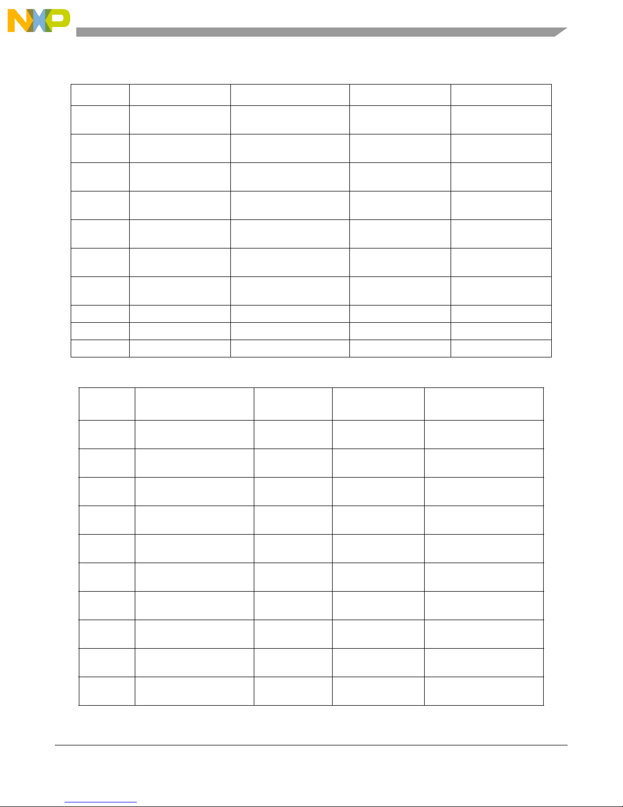
Interface Description
Table 16. Header J4 Signal Description
Interface Pin Signal Name MCU Signal Description Direction
5 ADC0_AN4 E[1] ADC module 0 channel
4 input
6 ADC0_AN5 E[2] ADC module 0 channel
5 input
7 ADC0_AN6 E[3] ADC module 0 channel
6 input
8 ADC0_AN7 E[4] ADC module 0 channel
7 input
9 ADC0_AN8 E[5] ADC module 0 channel
8 input
10 ADC0_AN9 E[6] ADC module 0 channel
9 input
11 ADC0_AN10 E[7] ADC module 0 channel
10 input
12 NC — — —
13 GNDA — Analog ground —
14 +3.3VA2 — +3.3V analog voltage —
Analog input
Analog input
Analog input
Analog input
Analog input
Analog input
Analog input
Table 17. Header J7 Signal Description
Interface
Pin
Signal Name MCU Signal Description Direction
1 ADC1_AN0 B[13] ADC module 1
channel 0 input
2 ADC1_AN1 B[14] ADC module 1
channel 1 input
3 ADC1_AN2 B[15] ADC module 1
channel 2 input
4 ADC1_AN3 C[0] ADC module 1
channel 3 input
5 ADC1_AN4 D[15] ADC module 1
channel 4 input
6 ADC1_AN5 E[0] ADC module 1
channel 5 input
7 ADC1_AN6 E[8] ADC module 1
channel 6 input
8 ADC1_AN7 E[9] ADC module 1
channel 7 input
9 ADC1_AN8 E[10] ADC module 1
channel 8 input
10 ADC1_AN9 E[11] ADC module 1
channel 9 input
Analog input
Analog input
Analog input
Analog input
Analog input
Analog input
Analog input
Analog input
Analog input
Analog input
MPC5604P Controller Board User’s Guide, Rev. 0
Freescale 17
Page 18
Interface Description
Table 17. Header J7 Signal Description
Interface
Pin
11 ADC1_AN10 E[12] ADC module 1
12 NC — — —
13 GNDA — Analog ground —
14 +3.3VA2 — +3.3V analogue
Signal Name MCU Signal Description Direction
Analog input
channel 10 input
—
voltage
Table 18. Header J9 Signal Description
Interface Pin Signal Name MCU Signal Description Direction
1 ADC0/1_AN11 B[9] ADC module 0/1
channel 11 input
2 ADC0/1_AN12 B[10] ADC module 0/1
channel 12 input
3 ADC0/1_AN13 B[11] ADC module 0/1
channel 13 input
4 ADC0/1_AN14 B[12] ADC module 0/1
channel 14 input
5 +3.3VA2 — +3.3V analogue voltage —
Analog input
Analog input
Analog input
Analog input
6 GNDA — Analog ground —
3.11 Header J3
Headers J3 allows monitoring the miscellaneous digital signals, see Table 19.
Table 19. Header J12 Signal Description
Interface Pin Signal Name MCU Port Description Direction
1 SCI0_TX B[2] Digital input/output Digital I/O
2 SCI0_RX B[3] Digital input/output Digital I/O
3 SPI3_SCK E[13] Digital input/output Digital I/O
4 SPI3_SOUT E[14] Digital input/output Digital I/O
5 SPI3_SIN E[15] Digital input/output Digital I/O
6 SPI3_CS0 F[3] Digital input/output Digital I/O
7GND — Ground—
8 +3.3Vdc — +3.3V voltage —
MPC5604P Controller Board User’s Guide, Rev. 0
Freescale18
Page 19

Design Consideration
4 Design Consideration
The MPC5604P Controller Board is designed for demonstration of the ability of Freescale MPC5604P
device to control various electrical motors and for easier development of the motor-control applications.
In addition to the hardware needed to run a motor, a variety of feedback signals that facilitate
control-algorithm development are provided. A set of schematics for the controller board appears in the
following section.
4.1 MPC5604P Features
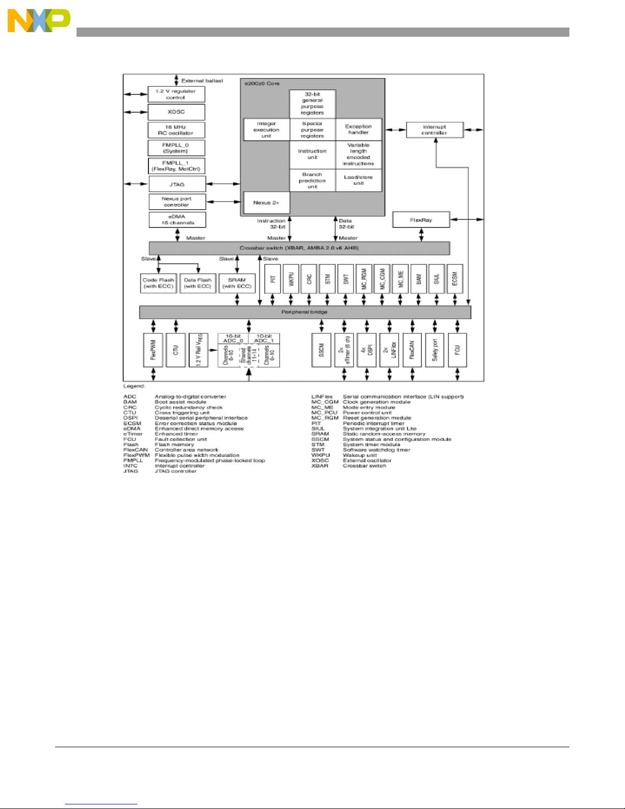
The MPC5604P is the first member of family of microcontrollers based on Power Architecture, targeted
at chassis and safety market segment, specifically at lower-end Electrical Power Steering and
airbag-application market space. The used core is the Harvard-bus interface version of the e200z0.
The MPC5604P has a single level of memory hierarchy consisting of 40 KB on-chip SRAM, 512+64 KB
of on-chip Flash memory. Both SRAM and Flash memory can hold instruction and data.
The timer functions of MPC5604P are performed by the eTimer — Modular Timer System and FlexPWM.
The two eTimer modules implement enhanced timer features (six channels each for a total of 12) including
dedicated motor-control quadrature-decode functionality and DMA support; FlexPWM module consists
of four submodules controlling a pair of PWM channels each; three submodules may be used to control
the three phases of a motor and the additional pair to support DC-DC converter width modulation control.
Off-chip communication is performed by a suite of serial protocols including FlexRay, CANs, enhanced
SPIs (DSPI), and SCIs (LinFlex).
The System Integration Unit Lite (SIUL) performs several chip-wide configuration functions. Pad
configuration and General-Purpose Input and Output (GPIO) are controlled from SIUL. External
interrupts and reset control are also found in the SIUL. The internal Multiplexer sub-block (IOMUX)
provides multiplexing of daisy chaining the DSPIs and external interrupt signal.
You can find detailed description of the MCU in the datasheet or reference manual.
MPC5604P Controller Board User’s Guide, Rev. 0
Freescale 19
Page 20
Design Consideration
Figure 4. MPC5604P Block Diagram
4.2 Clock Source
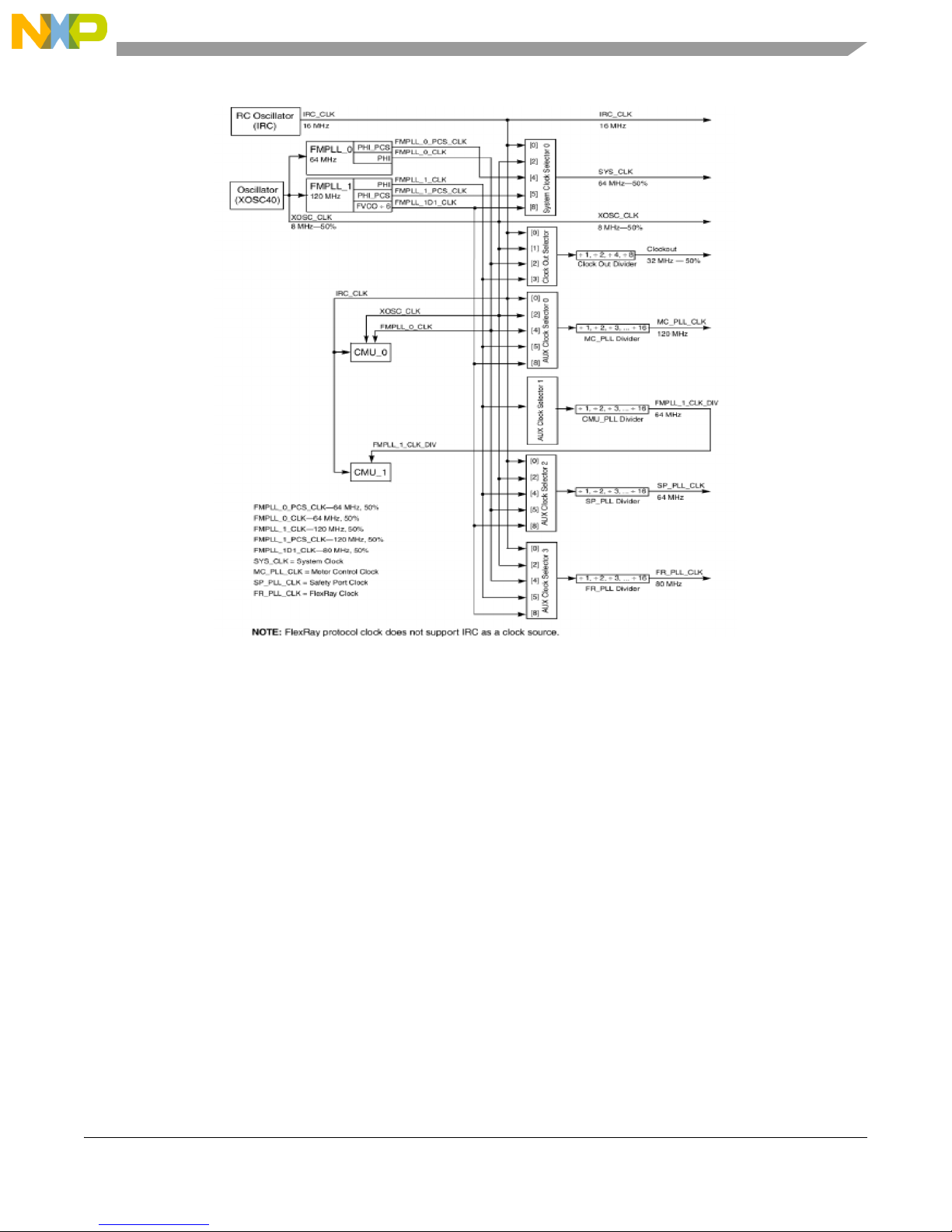
The MPC5604P uses external 8.00 MHz crystal oscillator mounted on the board and internal PLL0 to
multiply the input frequency, to achieve its 64 MHz maximum operating frequency. The second PLL1 is
used to achieve suitable frequency (120MHz) for internal Motor control, SWG, and communication
modules. The MPC5604P can also use internal 16 MHz RC oscillator as clock source, in this mode
FlexRAY protocol clock does not support IRCOSC as a clock source.
MPC5604P Controller Board User’s Guide, Rev. 0
Freescale20
Page 21
Design Consideration
Figure 5. MPC5604P Block Diagram
4.3 UNI3 Interfaces and External Fault Management
The motor power stages are controlled by microcontroller boards through two UNI3 and MC33937
connectors. The connector pin description was mentioned before in Section 3, “Interface Description.
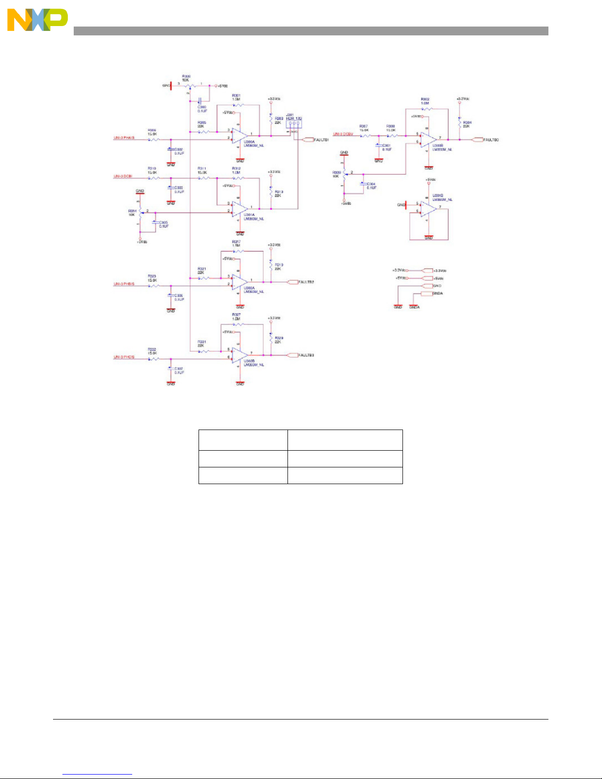
Analog or digital signals from the power stage M1 can be processed by hardware to maintain fault
management. The MPC5604P has four fault inputs and switch off PWM output signals in module.
The FAULT0 signal can be set up as under- or over-voltage. Whether the output signals from Phase A or
DCBUS over-current comparator can be asserted to the input FAULT1, depends on jumper position J301.
The FAULT2 and FAULT3 inputs can be used as over-current signals from phase B and C. The phase OC
level is set up by trimmer R300, as given in Figure 6.
MPC5604P Controller Board User’s Guide, Rev. 0
Freescale 21
Page 22
Design Consideration
Figure 6. FAULT Management
Table 20. Header J301 — FAULT1 Signal Assignment
Jumper Position Description
1-2 Phase A over-current
2-3 DC-bus-over current
4.4 Encoder/Hall Sensor Interface
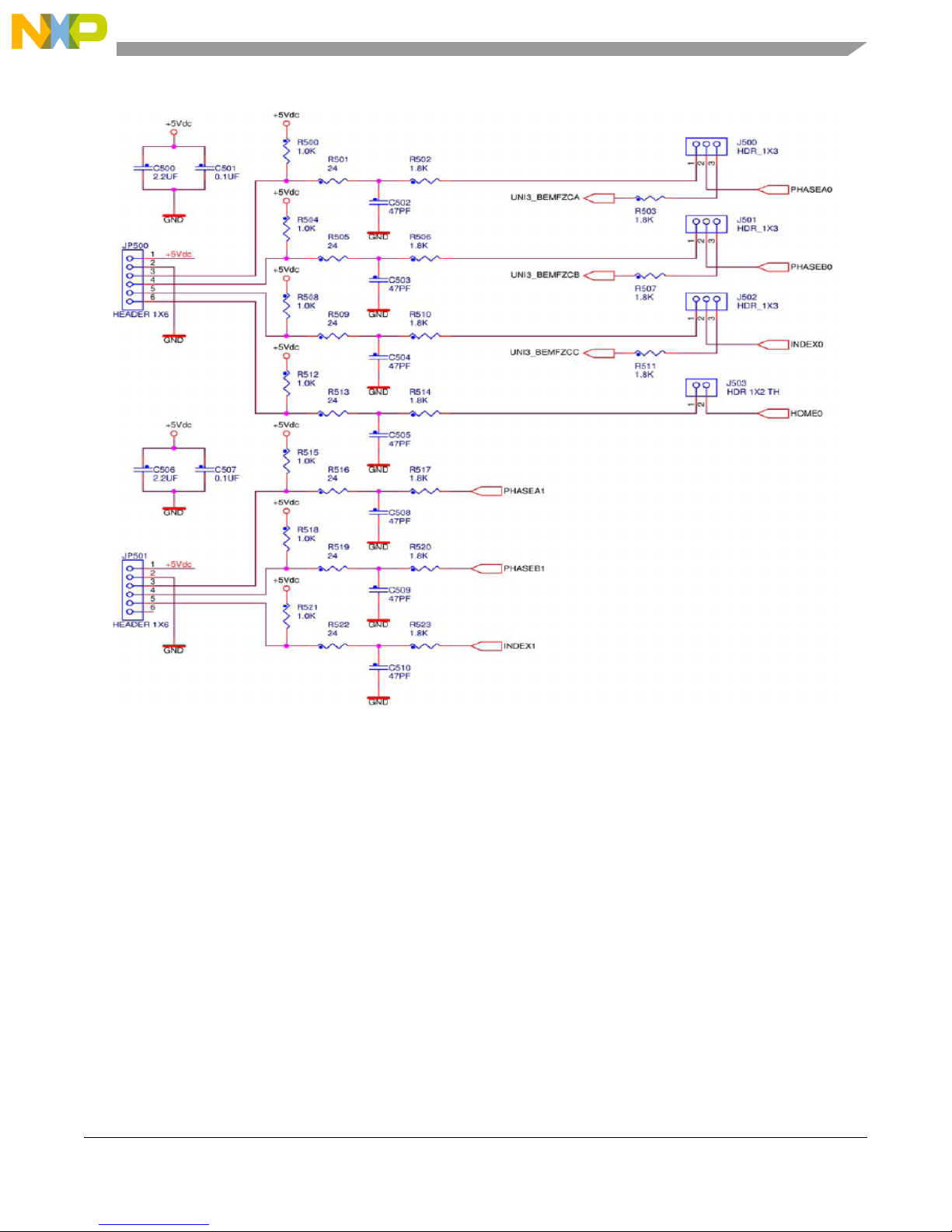
The motor control application can read position or speed from up to two independent encoders or HALL
sensors. The on-board interfaces provides the 5V power supply voltage to supply the sensors. The Hall
interface inputs are designed to support an open collector as well as push-pull Hall sensors outputs, see
Figure 7. A single pole RC low pass filter is present to reduce a signal noise.
MPC5604P Controller Board User’s Guide, Rev. 0
Freescale22
Page 23
Design Consideration
Figure 7. Encoder/Hall Sensor Interface Circuit
4.5 Resolver and SinCos Sensor Interface
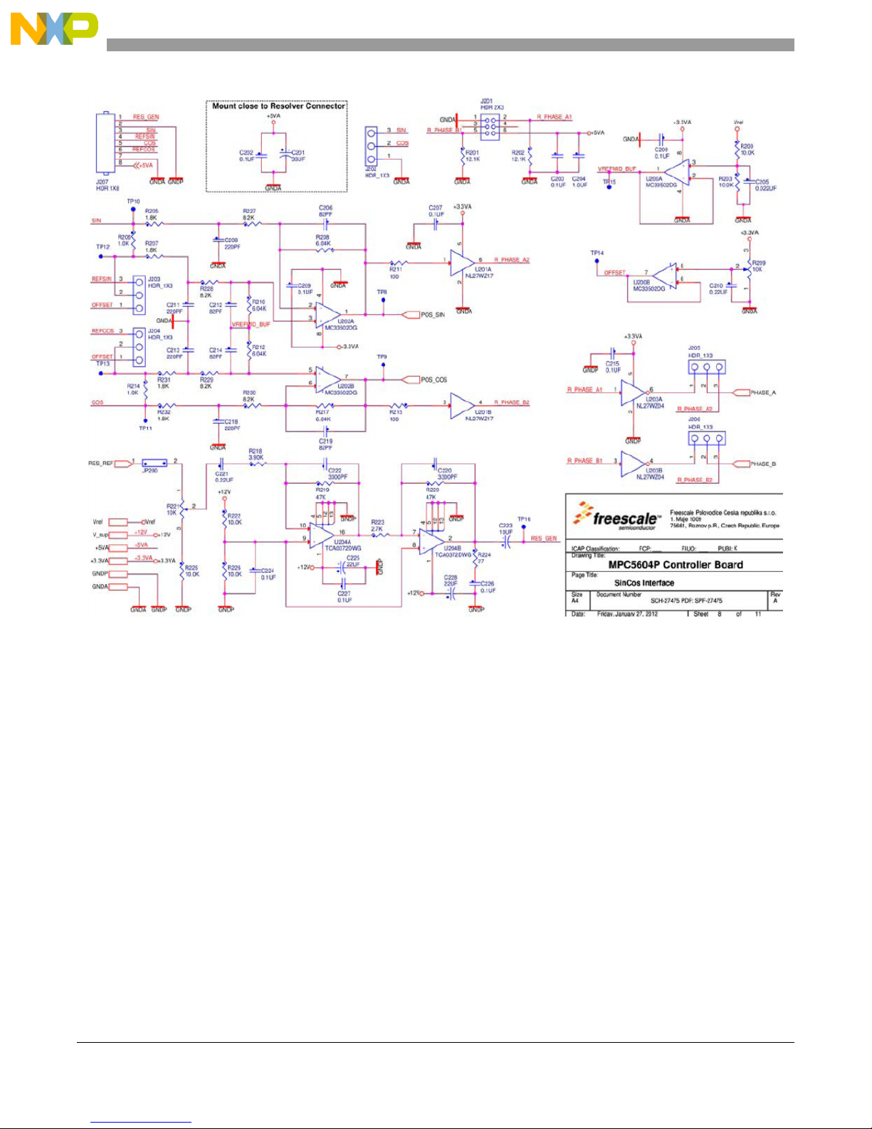
The resolver or SinCos interface is present on the board to observe actual motor rotor position.The board
is populated with hardware interface to allow measurement of motor rotor position and speed. Figure 8
shows resolver hardware circuitry. The resolver sensor can be connected through J207 connector. The
jumpers J203 and J204 provide selection of the positive input signal for differential amplifiers. In case of
use a resolver sensor, pins two and three should be shorted. The excitation signal output level (terminals
RES_GEN and GNDP) is set up by trimmer R221. The resolver excitation signal for resolver circuitry can
be selected by J2, the source signals are outputs from eTimer0.channel4 and eTimer0.channel5.
For detailed J207 connector signal description, see Table 8.
MPC5604P Controller Board User’s Guide, Rev. 0
Freescale 23
Page 24
Design Consideration
Figure 8. Resolver Interface Schematic
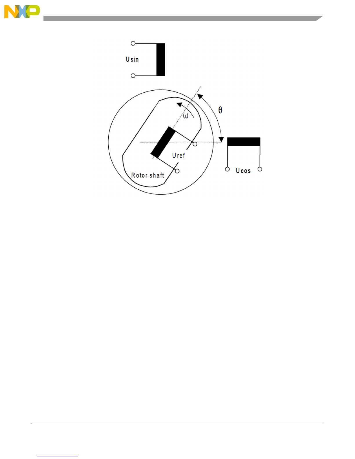
The resolver is an electro-mechanical transformer whose analog output voltages are a function of shaft
angle. It is, therefore, an absolute position transducer, providing true angular information at any time. The
reference winding (R1 and R2 terminals) is excited by an alternating signal Vref and output is taken from
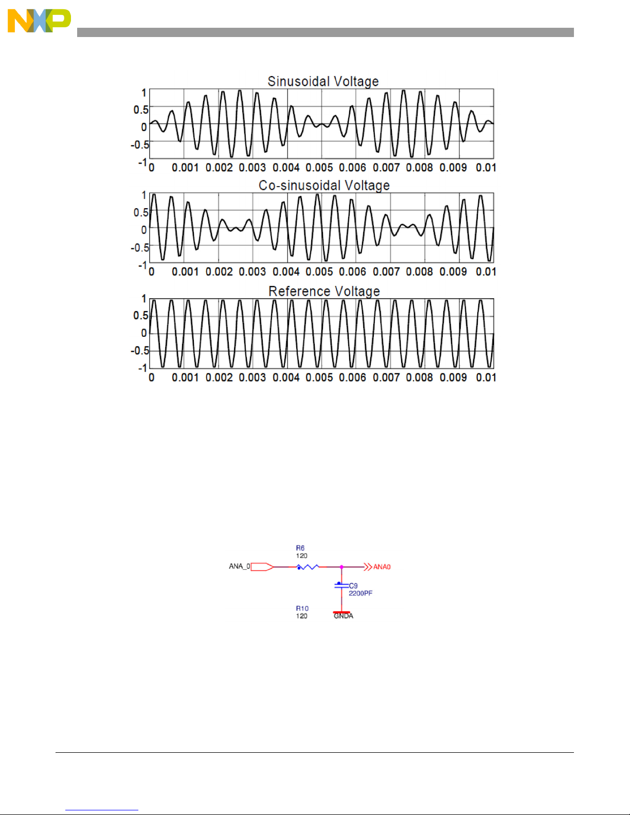
the two stator windings, as is depicted in Figure 9. The two stator windings fixed at right (90°) angles to
each other on the stator, produce a sine and co-sine feedback voltages Vsin, Vcos, respectively. However,
their amplitudes are modulated by sine and cosine as the shaft rotates, see Figure 10 in other words, the
voltages induced into the stator winding will be Vsin=K*sin()*sin(t) and Vsin=K*cos()*sin(t),
where K is the transformation ratio, is the shaft rotation from reference zero-degree position, and =2f
carrier frequency.
MPC5604P Controller Board User’s Guide, Rev. 0
Freescale24
Page 25
Design Consideration
Figure 9. Resolver Basics
These outputs are modified by a differential amplifiers and fed to an analog-to-digital converter. The rotor
angle can be extracted from these voltages using a digital approach. For detailed description, see
application note AN1942.
MPC5604P Controller Board User’s Guide, Rev. 0
Freescale 25
Page 26
Design Consideration
Figure 10. Resolver Excitation Signals
4.6 Analog Signal Sensing
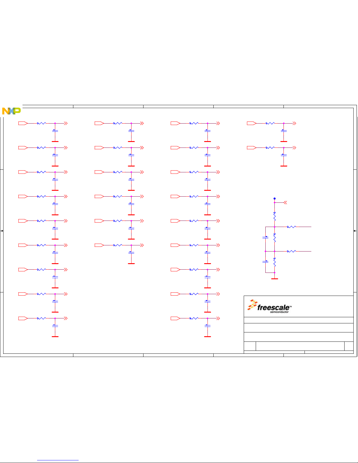
The MPC5604P can sample up to 2×16 analog signals. External 2×11 channels are connected through RC
filters directly to ADC converters zero and one, next four channels are common and can be internally
switched between both converters. They can be used to sample phase motor currents. The ADC0 channel
15 is dedicated for internal 1.2 V rail, and ADC1 channel 15 for the temperature sensor.
The time constant of RC filter should be set according to system requirements. The default time constant
was set to approximately 1.2 µs on the inputs zero to ten, and shared inputs are set to approximately 50 ns.
Figure 11. Analog Sensing Circuit
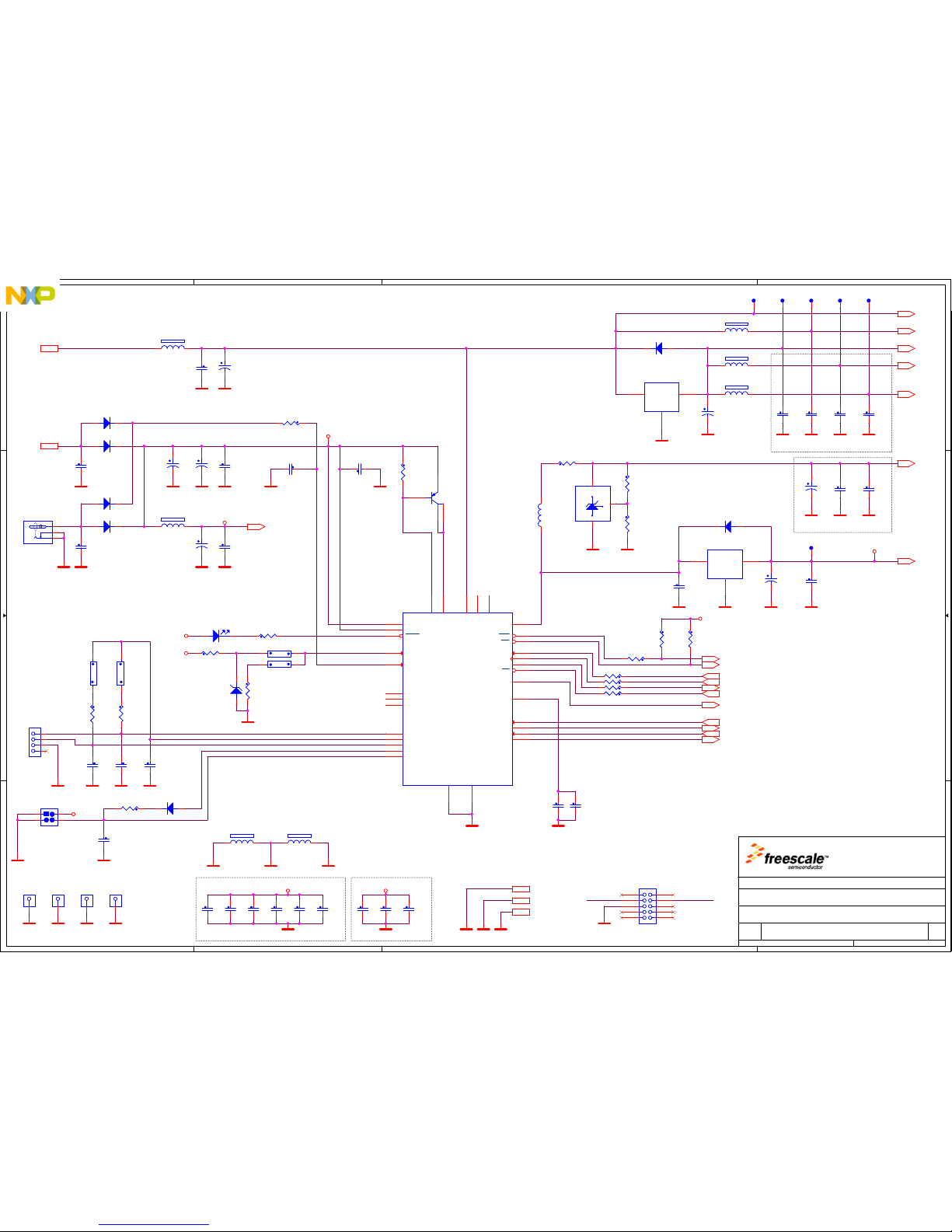
4.7 Power Supplies and Voltage Reference
The MPC5604P Controller Board can be supplied from three main power supply inputs. The first one uses
a 2.1 mm coaxial power jack and other one uses UNI-3 connector. Which one is more suitable depends on
MPC5604P Controller Board User’s Guide, Rev. 0
Freescale26
Page 27
Design Consideration
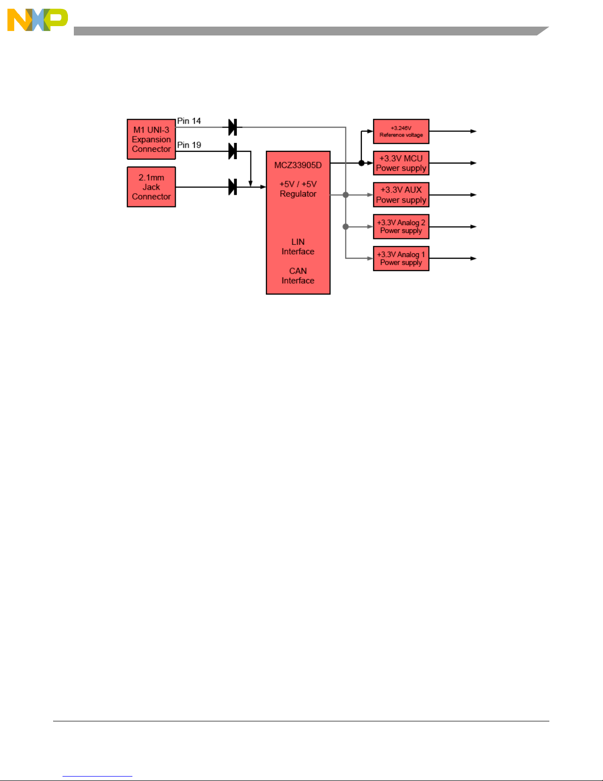
application type. The controller board provides a +5 V DC-voltage regulation for the resolver, encoder,
and FlexRAY driver, a +3.3 V DC-voltage regulation for MCU and supporting logic, and it provides
reference voltage for ADC module. The block diagram is shown in Figure 12.
Figure 12. Power Supply
4.8 UNI-3 PFC-PWM Signal (Power Factor Correction)
The PFC-PWM signal is used to additionally control the power stage circuit like PFC or power DC-DC
converter. These signals are connected to the MPC5604P controller pins GPIO G[6], and G[7].
4.9 UNI-3 Brake Signal
The brake signal is used to control the DC-bus resistor switch on connected power stage. It is accessible
via GPIO C[3].
4.10 CAN Bus
The FlexCAN module is a communication controller implementing the CAN protocol according to the
CAN 2.0B protocol specification, which supports both standard and extended message frames. A number
of Message Buffers (32) is also supported. Please refer to MPC5604P reference manual for detailed
description. Freescale system basis chip MC33905S with one CAN and one LIN interface is used as the
hardware interface for FlexCAN module. Jumpers JP1 and JP2 define middle or end node. The Safety
CAN module (Safety Port) doesn’t have a physical interface populated on the board but the signals are
accessible via header J13.
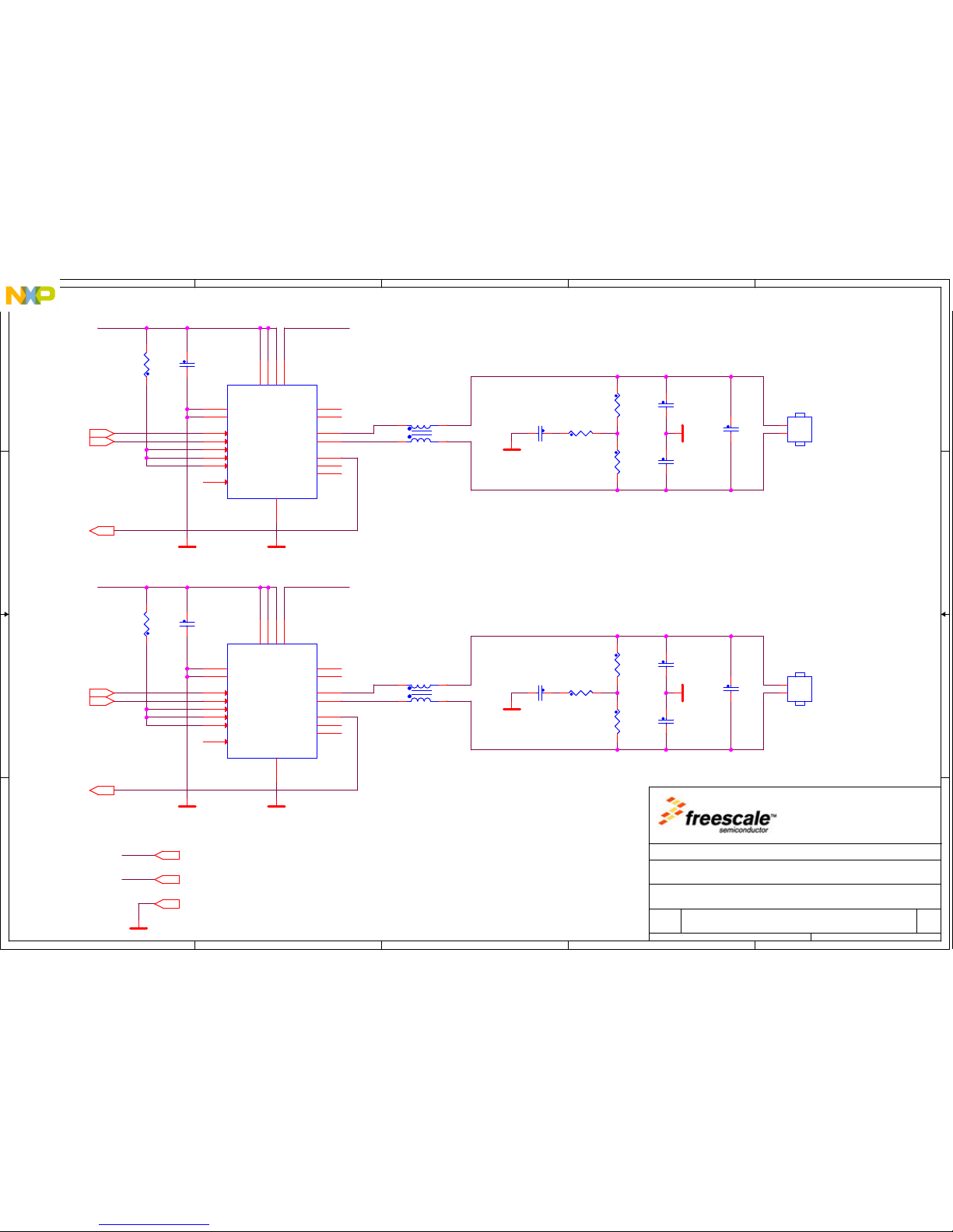
4.11 FlexRAY Interface
The FlexRAY module implements the FlexRay Communications System Protocol Specification, Version
2.1 Rev A. The hardware interface consists of two TJA1080 ICs, as shown in Figure 22.
MPC5604P Controller Board User’s Guide, Rev. 0
Freescale 27
Page 28
Electrical Characteristics
5 Electrical Characteristics
The electrical characteristics in Table 21 apply to an operation at 25 °C.
Table 21. Electrical Characteristics
Characteristic Symbol Min Typ Max Units
Power supply
Voltage
Current
consumption
Minimum Logic
one Input Voltage
Maximum Logic
zero Input Voltage
Input Logic
Resistance
Analog Input
Range
1
12V power supply, MCU without software
VDC 8 12 18 V
ICC — TBD — mA
1
VIH — — — mA
VIL — — — mA
RIN — 4.7 — K
0—3.3V
6 Board Set-Up Guide
The board is designed to be supplied either by the UNI-3 interface or by using the on-board J100 connector,
with a power supply voltage from 8 to 18V. When using the board as a standalone EVB, connect the power
supply to J100. In the case of board operation with the power stage is strongly recommended to supply the
board using the UNI-3 interface.
The MPC5604P Controller Board is designed for operation with the Freescale MC33937A based 3-Phase
low voltage power stage, see Figure 13 Development Kit can be ordered at. The complete 3-phase
BLDC/PMSM Sensor/Sensorless http://www.freescale.com.
Figure 13. 3-Phase Single PMSM Development Kit
MPC5604P Controller Board User’s Guide, Rev. 0
Freescale28
Page 29

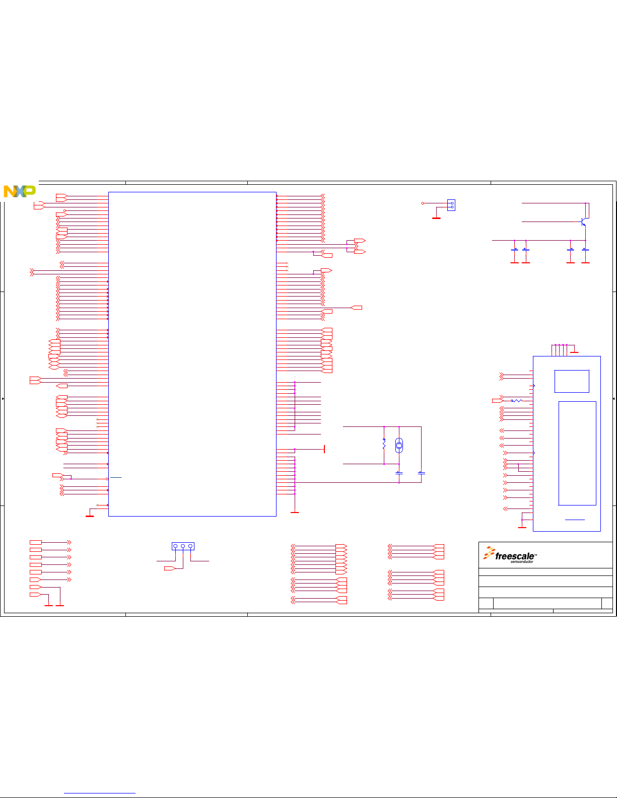
MPC5604P Controller Board Schematics
7 MPC5604P Controller Board Schematics
MPC5604P Controller Board User’s Guide, Rev. 0
Freescale 29
Page 30
5
5
4
4
3
3
2
2
1
1
D D
C C
B B
A A
Variant table
Agile # Variant
27475
27476
BLDC
PMSM
Rev
REVISIONS
Zone Date ApprovedDescription
MB27-Jan-12BLDC varian from 26776A
Rev
REVISIONS
Zone Date ApprovedDescription
MB27-Jan-12BLDC varian from 26776A
Rev
REVISIONS
Zone Date ApprovedDescription
MB27-Jan-12BLDC varian from 26776A
Drawing Title:
Size Document Number Rev
Date: Sheet
of
Page Title:
ICAP Classification: FCP: FIUO: PUBI:
SCH-27475 PDF: SPF-27475 A
MPC5604P Controller Board
A4
Friday, January 27, 2012
REVISIONS
1 11
___ X
___
1. Maje 1009
75661, Roznov p.R., Czech Republic, Europe
Freescale Polovodice Ceska republika s.r.o.
Drawing Title:
Size Document Number Rev
Date: Sheet of
Page Title:
ICAP Classification: FCP: FIUO: PUBI:
SCH-27475 PDF: SPF-27475 A
MPC5604P Controller Board
A4
Friday, January 27, 2012
REVISIONS
1 11
___ X
___
1. Maje 1009
75661, Roznov p.R., Czech Republic, Europe
Freescale Polovodice Ceska republika s.r.o.
Drawing Title:
Size Document Number Rev
Date: Sheet of
Page Title:
ICAP Classification: FCP: FIUO: PUBI:
SCH-27475 PDF: SPF-27475 A
MPC5604P Controller Board
A4
Friday, January 27, 2012
REVISIONS
1 11
___ X
___
1. Maje 1009
75661, Roznov p.R., Czech Republic, Europe
Freescale Polovodice Ceska republika s.r.o.
Page 31
5
5
4
4
3
3
2
2
1
1
D D
C C
B B
A A
Numbering: 0 - 199
MCU_3.3V
/RST
+3.3VA2
+3.3VA1
+5VA
PER_3.3V
+5Vdc
+12V
GND
GNDA
GNDP
MCU_3.3V
GND GNDA GNDP
GND GNDA
GND
GNDGNDA
GNDPGNDA
GND
+3.3VA1 +3.3VA2
+5VA+12V
PER_3.3V
+5Vdc
+3.3VA1
+5VA
PER_3.3V
+12V
+5Vdc
+3.3VA2
GNDAGND GNDP
MCU_3.3V
MCU_3.3V
Drawing Title:
Size Document Number Rev
Date: Sheet of
Page Title:
ICAP Classification: FCP: FIUO: PUBI:
SCH-27475 PDF: SPF-27475 A
MPC5604P Controller Board
A3
Friday, January 27, 2012
Hierarchical view
2 11
___ X
___
1. Maje 1009
75661, Roznov p.R., Czech Republic, Europe
Freescale Polovodice Ceska republika s.r.o.
Drawing Title:
Size Document Number Rev
Date: Sheet of
Page Title:
ICAP Classification: FCP: FIUO: PUBI:
SCH-27475 PDF: SPF-27475 A
MPC5604P Controller Board
A3
Friday, January 27, 2012
Hierarchical view
2 11
___ X
___
1. Maje 1009
75661, Roznov p.R., Czech Republic, Europe
Freescale Polovodice Ceska republika s.r.o.
Drawing Title:
Size Document Number Rev
Date: Sheet of
Page Title:
ICAP Classification: FCP: FIUO: PUBI:
SCH-27475 PDF: SPF-27475 A
MPC5604P Controller Board
A3
Friday, January 27, 2012
Hierarchical view
2 11
___ X
___
1. Maje 1009
75661, Roznov p.R., Czech Republic, Europe
Freescale Polovodice Ceska republika s.r.o.
ENCODERS
ENCODERS
PHASEA0
PHASEA1
PHASEB0
PHASEB1
INDEX0
INDEX1
HOME0
+5Vdc
GND
UNI3_BEMFZCA
UNI3_BEMFZCB
UNI3_BEMFZCC
MCU
MCU
CAN_TX_PHY
CAN_RX_PHY
CAN_EN
CAN_STBY
CAN_NERR
FR_A_TX
FR_B_TX
FR_A_RX
FR_B_RX
/FR_B_TX_EN
/FR_A_TX_EN
PHASE_A
PHASE_B
RES_REF
ANA_0
ANA_1
ANA_2
ANA_3
ANA_4
ANA_5
ANA_6
ANA_7
ANB_0
ANB_1
ANB_2
ANB_3
ANB_4
ANB_5
ANB_6
ANB_7
PHASEA0
PHASEA1
PHASEB0
PHASEB1
INDEX0
INDEX1
HOME0
FAULTB0
FAULTB1
FAULTB2
FAULTB3
PWMA0
PWMB0
PWMA1
PWMB1
PWMA2
PWMB2
PWM_X0
PWM_X1
PWM_X2
PWM_X3
PWMA3
PWMB3
ANA_8
ANA_9
ANA_10
AN_11
AN_12
AN_13
AN_14
ANB_8
ANB_9
ANB_10
+3.3Vdc
VREF
GND
GNDA
+3.3VA2
+5Vdc
+12V
EIRQ#22
SAFETY_CAN_TX_PHY
SAFETY_CAN_RX_PHY
DSPIO_SIN
DSPIO_CS
DSPIO_SCK
DSPIO_SOUT
SCI1_TX
SCI1_RX
SPI3_SIN
MCU_3.3V
G[1]
G[0]
SPI3_SOUT
SPI3_SCK
SPI3_CS0
C[10]
C[9]
C[8]
/RST
D[5]
PSU
POWER SUPPLY
+3.3VA1
+3.3VA2
+5Vdc
+5VA
Vref
GNDP
GNDA
UNI3_15V
GND
UNI3_5V
+12V
LIN_TX
33905_SCLK
CAN_TX_PHY
MCU_3.3V
33905_/CS
33905_/INT
MUX_OUT
33905_/RST
CAN_RX_PHY
33905_MOSI
33905_MISO
PER_3.3V
LIN_RX
UNI3
UNI3
PWM0
PWM1
PWM2
PWM3
PWM4
PWM5
UNI-3 +5V
UNI-3 +15VA
UNI3_BEMFZCA
UNI3_BEMFZCB
UNI3_BEMFZCC
SERIAL
BRAKE
PFC
PFC_EN
PFC_ZC
FAULTB0
FAULTB1
FAULTB2
FAULTB3
GNDA
GND
+3.3Vdc
+5Vdc
PHCIS
DCBV
TEMP
DCBI
PHAIS
PHBIS
33937_SIN
33937_SOUT
33937_SCK
33937_CS
33937_/RST
33937_OC
33937_EN
33937_INT
FlexRay
FlexRay_DRV
GND
V_sup
+5Vdc
FR_A_TX
FR_B_TX
/FR_A_TX_EN
/FR_B_TX_EN
FR_B_RX
FR_A_RX
Resolver/SINCOS
Resolvers
+3.3VA
POS_SIN
POS_COS
PHASE_A
PHASE_B
RES_REF
V_sup
GNDA
Vref
GNDP
+5VA
Page 32
5
5
4
4
3
3
2
2
1
1
D D
C C
B B
A A
CLOCK CIRCUIT
CORE SUPPLY CIRCUIT
NEXUS INTERFACE
BOOT SELECTION
XTAL
EXTAL
XTAL
VSSA
BCTRL
FAULTB1
FAULTB0
FAULTB2
FAULTB3
PWMA0
SCI0_TX
SCI0_RX
SCI1_TX
SCI1_RX
PWMA3
PHASEA0
PHASEB0
INDEX0
HOME0
ET0_4
ET0_5
PWM_X2
PWM_X1
ET0_4 ET0_5
PHASE_B
PHASE_A
VDD_CORE
VDD_CORE
VDD_CORE
MCU_3.3V
VDD_LV_PLL
Vref
Vref
VDD_CORE
VDD_LV_PLL
Vref
PWMB3
PWMA2
PWMB2
PWM_X3
PWM_X0
PWMB0
+5Vdc
+3.3VA2
+12V
EXTAL
PWMA0
PWMA1
PWMA2
PWMA3
PWMB0
PWMB1
PWMB2
PWM_X0
PWM_X1
PWM_X2
PWM_X3
PHASE_A
PHASE_B
PWMB3
FAULTB0
FAULTB1
FAULTB2
FAULTB3
PHASEA0
PHASEB0
INDEX0
HOME0
PHASEA1
PHASEB1
INDEX1
PWMA1
PWMB1
+3.3Vdc
+12V
BCTRL
MCU_3.3V
MCU_3.3V
INDEX1
PHASEB1
PHASEA1
VSS_HV_OSC
VDD_CORE
/FR_A_TX_EN
/FR_B_TX_EN
FR_A_TX
FR_B_TX
FR_A_RX
FR_B_RX
CAN_EN
CAN_NERR
PHASEA0
PHASEB0
INDEX0
HOME0
PHASE_A
PHASE_B
RES_REF
VREF
GND
GNDA
FAULTB0
FAULTB1
FAULTB2
FAULTB3
PWMA0
PWMB0
PWMA1
PWMB1
PWMA2
PWMB2
PWM_X0
PWM_X1
PWM_X2
PWM_X3
PWMA3
PWMB3
+3.3Vdc
+5Vdc
+3.3VA2
+12V
EIRQ#22
FAULTB0
FAULTB1
FAULTB2
FAULTB3
PWMA2
PWMB2
PWM_X2
PWM_X3
PWMA3
PWMB3
PHASE_A
PWMA0
PWMB0
PWMA1
PWMB1
PWM_X0
PWM_X1
PHASEB1
INDEX1
PHASE_B
PHASEA0
PHASEB0
INDEX0
HOME0
PHASEA1
CAN_STBY
PHASEA1
DSPIO_CS
DSPIO_SIN
DSPIO_SCK
DSPIO_SOUT
SPI3_SIN
SPI3_CS0
SPI3_SOUT
SPI3_SCK
G[0]
G[1]
MCU_3.3V
INDEX1
PHASEB1
PHASEA1
C[8]
C[9]
C[10]
/RST
D[5]
GNDGND
GND
GND
GNDA
GNDGNDA
GND
FAB
FAB
GND
GND GND
GND
ANA0
ANA1
ANA2
ANA3
ANA4
ANA5
ANA6
ANA7
ANA8
ANA9
ANA10
AN11
AN12
ANB0
ANB1
ANB2
ANB3
ANB4
ANB5
ANB6
ANB7
ANB8
ANB9
ANB10
AN13
AN14
RESET
TMS
TCK
TDI
TDO
EVTI
EVTO
MDO1
MDO2
MDO3
MCKO
MSEO0
MSEO1
MDO0
CLKOUT
EIRQ#6
EIRQ#7
ON/OFF
GPIOA12
GPIOA13
SCI1_RX
SCI1_TX
SPI3_SIN
SPI3_SOUT
SPI3_SCK
SPI3_CS0
SAFETY_CAN_TX
SAFETY_CAN_RX
Vref
+12V
+3.3VA2
CAN_TX
CAN_RX
PWMA0
PWMA1
PWMA2
PWMA3
PWMB0
PWMB1
PWMB2
PWM_X0
PWM_X1
PWM_X2
PWM_X3
PHASE_A
PHASE_B
PWMB3
FAULTB0
FAULTB1
FAULTB2
FAULTB3
PHASEA0
PHASEA1
PHASEB0
PHASEB1
INDEX0
INDEX1
HOME0
+5Vdc
+3.3Vdc
JCOMP
MSEO0
MSEO1
MCKO
MCU_3.3V
+12V
MCU_3.3V
EVTO
CLKOUT
MDO0
MDO1
MDO2
EVTI
MDO3
RESET
TDO
TDI
TMS
TCK
ETO_4
ETO_5
MCU_3.3V
SCI0_RX
SCI0_TX
Drawing Title:
Size Document Number Rev
Date: Sheet of
Page Title:
ICAP Classification: FCP: FIUO: PUBI:
SCH-27475 PDF: SPF-27475 A
MPC5604P Controller Board
A3
Friday, January 27, 2012
MCU
3 11
___ X
___
1. Maje 1009
75661, Roznov p.R., Czech Republic, Europe
Freescale Polovodice Ceska republika s.r.o.
Drawing Title:
Size Document Number Rev
Date: Sheet of
Page Title:
ICAP Classification: FCP: FIUO: PUBI:
SCH-27475 PDF: SPF-27475 A
MPC5604P Controller Board
A3
Friday, January 27, 2012
MCU
3 11
___ X
___
1. Maje 1009
75661, Roznov p.R., Czech Republic, Europe
Freescale Polovodice Ceska republika s.r.o.
Drawing Title:
Size Document Number Rev
Date: Sheet of
Page Title:
ICAP Classification: FCP: FIUO: PUBI:
SCH-27475 PDF: SPF-27475 A
MPC5604P Controller Board
A3
Friday, January 27, 2012
MCU
3 11
___ X
___
1. Maje 1009
75661, Roznov p.R., Czech Republic, Europe
Freescale Polovodice Ceska republika s.r.o.
R5
1.0M
C339
0.1 UF
20
D15EVEN
D14EVEN
D13EVEN
D12EVEN
D11EVEN
D10EVEN
D9EVEN
D8EVEN
POD3-6
POD3-5
POD3-4
POD3-3
POD3-2
POD3-1
POD2-0
4
5
6
7
8
9
10
11 POD3-0
POD2-7
POD2-6
GROUND
39,40,41,42,43
Note: This connector
is numbered Tek style
1
2
TEKPIN
D15ODD
D14ODD
D13ODD
D12ODD
D11ODD
D9ODD
D8ODD
:
19
38
37
:
D2ODD
D1ODD
D0ODD
POD1-7
POD1-6
POD1-5
POD1-4
POD1-3
POD1-1
D7EVEN
D6EVEN
D5EVEN
D4EVEN
D3EVEN
D2EVEN
D1EVEN
D0EVEN
POD3-7
35
34
33
32
31
29
28
27
26
POD2-5
POD2-4
POD2-3
POD2-2
POD2-1
POD0-2
POD0-1
POD0-0
25
24
23
22
21
20
12
13
14
15
16
17
18
19
HP
CLK_EVEN
CKQ_0_33
CLK_ODDCKQ_1_236
D10ODDPOD1-230
D7ODD
D6ODD
D5ODD
D4ODD
D3ODD
POD1-0
POD0-7
POD0-6
POD0-5
POD0-4
POD0-3
J310
5767054-1
POD3_3
8
LA5V
1
POD3_2
9
GROUND1
20
POD0_1
21
POD0_2
22
POD0_3
23
POD0_4
24
POD0_5
25
POD0_6
26
POD0_7
27
POD1_0
28
POD1_1
29
POD1_2
30
POD1_3
31
POD1_4
32
POD1_5
33
POD1_6
34
POD1_7
35
CLK_ODD
36
SDA
37
POD3_0
11
POD3_6
5
POD3_5
6
SCL
38
GROUND2
2
POD3_7
4
CLK_EVEN
3
POD2_7
12
POD2_0
19
POD2_1
18
POD2_2
17
POD2_3
16
POD2_4
15
POD2_5
14
POD2_6
13
POD3_1
10
POD3_4
7
GND139GND240GND341GND442GND5
43
R338
0
J2
HDR_1X3
123
Y1
8MHz
1 2
J312
HDR_1X2_M
1
2
C7
22PF
C8
22PF
C5
2.2UF
MPC5604P
U1
A[0]/ETIMER0_ETC[0]
73
A[1]/ETIMER0_ETC[1]
74
A[2]/ETIMER0_ETC[2]
84
A[3]/ETIMER0_ETC[3]
92
A[4]/ETIMER1_ETC[0]
108
A[5]/DSPI1_CS0
14
A[6]/DSPI1_SCK
2
A[7]/DSPI1_SOUT
10
A[8]/DSPI1_SIN
12
A[9]/DSPI2_CS1
134
A[10]/DSPI2_CS0
118
A[11]/DSPI2_SCK
120
A[12]/DSPI2_SOUT
122
A[13]/DSPI2_SIN
136
A[14]/SAFETYPORT0_TXD
143
A[15]/SAFETYPORT0_RXD
144
B[0]/CAN0_TXD
109
B[1]/CAN0_RXD
110
B[2]/LIN0_TXD
114
B[3]/LIN0_RXD
116
B[4]/JTAG0_TDO
89
B[5]/JTAG0_TDI
86
B[6]/CLKOUT/DSPI2_CS2
138
B[7]/ADC0_AN[0]
43
B[8]/ADC0_AN[1]
47
B[9]/ADC0_ADC1_AN[11]
52
B[10]/ADC0_ADC1_AN[12]
53
B[11]/ADC0_ADC1_AN[13]
54
B[12]/ADC0_ADC1_AN[14]
55
B[13]/ADC1_AN[0]
60
B[14]/ADC1_AN[1]
64
B[15]/ADC1_AN[2]
62
C[0]/ADC1_AN[3]
66
C[1]/ADC0_AN[2]
41
C[2]/ADC0_AN[3]
45
C[3]/DSPI0_CS1
16
C[4]/DSPI0_CS0
11
C[5]/DSPI0_SCK
13
C[6]/DSPI0_SOUT
142
C[7]/DSPI0_SIN
15
C[8]/DSPI1_CS1
130
C[9]/DSPI2_CS3
123
C[10]/DSPI2_CS2
111
C[11]/ETIMER0_ETC[4]
80
C[12]/ETIMER0_ETC[5]
82
C[13]/ETIMER1_ETC[1]
101
C[14]/ETIMER1_ETC[2]
103
C[15]/FLEXRAY0_CA_TR_EN
124
D[0]/FLEXRAY0_CA_TX
125
D[1]/FLEXRAY0_CA_RX
3
D[2]/FLEXRAY0_CB_RX
140
D[3]/FLEXRAY0_CB_TX
128
D[4]/FLEXRAY0_CB_TR_EN
129
D[5]/DSPI0_CS3
33
D[6]/DSPI0_CS2
34
D[7]/DSPI1_CS3
37
D[8]/DSPI1_CS2
32
D[9]/FLEXPWM0_X[0]
26
D[10]/FLEXPWM0_A[0]
76
D[11]/FLEXPWM0_B[0]
78
D[12]/FLEXPWM0_X[1]
99
D[13]/FLEXPWM0_A[1]
95
D[14]/FLEXPWM0_B[1]
105
D[15]/ADC1_AN[4]
58
E[0]/ADC1_AN[5]
68
E[1]/ADC0_AN[4]
39
E[2]/ADC0_AN[5]
49
E[3]/ADC0_AN[6]
40
E[4]/ADC0_AN[7]
42
E[5]/ADC0_AN[8]
44
E[6]/ADC0_AN[9]
46
E[7]/ADC0_AN[10]
48
E[8]/ADC1_AN[6]
59
E[9]/ADC1_AN[7]
61
E[10]/ADC1_AN[8]
63
E[11]/ADC1_AN[9]
65
E[12]/ADC1_AN[10]
67
E[13]/DSPI3_SCK
117
E[14]/DSPI3_SOUT
119
E[15]/DSPI3_SIN
121
F[0]/FLEXRAY0_DBG0
133
F[1]/FLEXRAY0_DBG1
135
F[2]/FLEXRAY0_DBG2
137
F[3]/FLEXRAY0_DBG3
139
F[4]/NEXUS0_MDO[3]
4
F[5]/NEXUS0_MDO[2]
5
F[6]/NEXUS0_MDO[1]
8
F[7]/NEXUS0_MCKO
19
F[8]/NEXUS0_MSEO1
20
F[9]/NEXUS0_MSEO0
23
F[10]/NEXUS0_EVTO
24
F[11]/NEXUS0_EVTI
25
F[12]/ETIMER1_ETC[3]
106
F[13]/ETIMER1_ETC[4]
112
F[14]/LIN1_TXD
115
F[15]/LIN1_RXD
113
G[0]/FCU0_F[0]
38
G[1]/FCU0_F[1]
141
G[2]/FLEXPWM0_X[2]
102
G[3]/FLEXPWM0_A[2]
104
G[4]/FLEXPWM0_B[2]
100
G[5]/FLEXPWM0_X[3]
85
G[6]/FLEXPWM0_A[3]
98
G[7]/FLEXPWM0_B[3]
83
G[8]/FLEXPWM0_FAULT[0]
81
G[9]/FLEXPWM0_FAULT[1]
79
G[10]/FLEXPWM0_FAULT[2]
77
G[11]/FLEXPWM0_FAULT[3]
75
MDO_0
9
NMI
1
XTAL
29
EXTAL
30
TMS
87
TCK
88
RESET
31
VPP_TEST
107
VSS_LV_REGCOR
71
VSS_HV_FL
96
VSS_LV_PLL
35
VSS_HV_OSC0
28
VSS_LV_COR2
132
VSS_LV_COR1
94
VSS_LV_COR0
17
VSS_HV_IO3
127
VSS_HV_IO2
90
VSS_HV_IO1
22
VSS_HV_IO0
7
VSS_HV_AD1
57
VSS_HV_AD0
51
VDD_HV_IO0
6
VDD_HV_IO1
21
VDD_HV_IO2
91
VDD_HV_IO3
126
VDD_LV_COR0
18
VDD_LV_COR1
93
VDD_LV_COR2
131
VDD_HV_REG
72
VDD_LV_PLL
36
VDD_HV_AD0
50
VDD_HV_AD1
56
VDD_LV_REGCOR
70
VDD_HV_FL
97
VDD_HV_OSC
27
BCTRL
69
C6
0.1 UF
E
B
C
Q1
BCP68
1
3 2
4
C340
2.2UF
Page 33
5
5
4
4
3
3
2
2
1
1
D D
C C
B B
A A
Place filters as close to the DSP chip as possible
AN_14
ANB_7
ANA_0
ANA_1
ANA_2
ANA_3
ANA_4
ANA_5
ANA_6
ANA_7
ANB_0
ANB_1
ANB_2
ANB_3
ANB_4
ANB_5
ANB_6
ANB_7
ANB_8ANA_8
AN_12
ANA_9
ANA_10
AN_11
AN_14
AN_13
ANB_9
ANB_10
GNDA GNDA
GNDA
GNDAGNDA
GNDA
GNDA GNDA
GNDA GNDA
GNDAGNDA
GNDA GNDA
GNDAGNDA
GNDA
GNDAGNDA
GNDA
GNDA
GNDA
GNDA
GNDA
GNDA
GNDA
GNDA
ANA6
ANA7
ANA4
ANA5 ANB5
ANB2
ANB7
ANB3
ANB0
ANB1
ANB6
ANB4
ANA0
ANA1
ANA2
ANA3
ANA8 ANB8
AN12
ANA10
AN11
ANA9
AN14
AN13
ANB10
ANB9
Vref
Drawing Title:
Size Document Number Rev
Date: Sheet of
Page Title:
ICAP Classification: FCP: FIUO: PUBI:
SCH-27475 PDF: SPF-27475 A
MPC5604P Controller Board
A4
Friday, January 27, 2012
ADC FILTERS
4 11
___ X
___
1. Maje 1009
75661, Roznov p.R., Czech Republic, Europe
Freescale Polovodice Ceska republika s.r.o.
Drawing Title:
Size Document Number Rev
Date: Sheet of
Page Title:
ICAP Classification: FCP: FIUO: PUBI:
SCH-27475 PDF: SPF-27475 A
MPC5604P Controller Board
A4
Friday, January 27, 2012
ADC FILTERS
4 11
___ X
___
1. Maje 1009
75661, Roznov p.R., Czech Republic, Europe
Freescale Polovodice Ceska republika s.r.o.
Drawing Title:
Size Document Number Rev
Date: Sheet of
Page Title:
ICAP Classification: FCP: FIUO: PUBI:
SCH-27475 PDF: SPF-27475 A
MPC5604P Controller Board
A4
Friday, January 27, 2012
ADC FILTERS
4 11
___ X
___
1. Maje 1009
75661, Roznov p.R., Czech Republic, Europe
Freescale Polovodice Ceska republika s.r.o.
C34
2200PF
C16
2200PF
R35
120
C19
82PF
C28
2200PF
C25
2200PF
R13
120
C35
2200PF
R28
120
R34
120
C30
0.022UF
R10
120
R17
120
R24
0
R22
120
R27
120
R25
2K
C23
2200PF
C24
82PF
C13
2200PF
R23
120
C15
2200PF
R21
120
C27
2200PF
C29
2200PF
R29
0
R16
120
R7
120
C22
2200PF
C11
2200PF
R18
120
R20
1.0K
C17
2200PF
C33
2200PF
C21
82PF
TP1
R32
120
R15
120
C31
2200PF
R14
120
C10
2200PF
R12
120
R31
120
C26
0.022UF
C18
82PF
R33
120
R19
120
C14
2200PF
C32
2200PF
R26
120
R11
120
R6
120
R9
120
C36
2200PF
C20
2200PF
C9
2200PF
R36
120
R30
1.0K
R8
120
C12
2200PF
Page 34
5
5
4
4
3
3
2
2
1
1
D D
C C
B B
A A
FlexRay A CIRCUIT
FlexRay B CIRCUIT
V_sup
VSUP
+5Vdc
+5Vdc
+5Vdc V_sup
FR_B_RX
FR_B_TX
/FR_B_TX_EN
/FR_A_TX_EN
FR_A_RX
FR_A_TX
V_sup
+5Vdc
GND
GNDGND
GND
GND
GNDGND
GND
GND
GND
Drawing Title:
Size Document Number Rev
Date: Sheet of
Page Title:
ICAP Classification: FCP: FIUO: PUBI:
SCH-27475 PDF: SPF-27475 A
MPC5604P Controller Board
A4
Friday, January 27, 2012
FlexRay Interface
5 11
___ X
___
1. Maje 1009
75661, Roznov p.R., Czech Republic, Europe
Freescale Polovodice Ceska republika s.r.o.
Drawing Title:
Size Document Number Rev
Date: Sheet of
Page Title:
ICAP Classification: FCP: FIUO: PUBI:
SCH-27475 PDF: SPF-27475 A
MPC5604P Controller Board
A4
Friday, January 27, 2012
FlexRay Interface
5 11
___ X
___
1. Maje 1009
75661, Roznov p.R., Czech Republic, Europe
Freescale Polovodice Ceska republika s.r.o.
Drawing Title:
Size Document Number Rev
Date: Sheet of
Page Title:
ICAP Classification: FCP: FIUO: PUBI:
SCH-27475 PDF: SPF-27475 A
MPC5604P Controller Board
A4
Friday, January 27, 2012
FlexRay Interface
5 11
___ X
___
1. Maje 1009
75661, Roznov p.R., Czech Republic, Europe
Freescale Polovodice Ceska republika s.r.o.
C603
33PF
L600
ACM4532-801-2P-T001
41
2 3
R603
47
R605
47
C608
33PF
C600
0.1UF
C605
0.1UF
C602
0.047UF
C601
47PF
C607
0.047UF
R601
47
R600
3.3K
R604
3.3K
J601
53261-0219
1
2
R606
10
C609
47PF
R602
10
C604
47PF
L601
ACM4532-801-2P-T001
41
2 3
U600
TJA1080TS/N
TRXD0
11
TRXD1
10
TXD
5
TXEN
6
BGE
8
STBN
9
EN
3
WAKE
15
INH2
1
INH1
2
BP
18
BM
17
RXD
7
ERRN
13
RXEN
12
VIO
4
VCC
19
VBUF
20
VBAT
14
GND
16
R607
47
C606
47PF
J600
53261-0219
1
2
U601
TJA1080TS/N
TRXD0
11
TRXD1
10
TXD
5
TXEN
6
BGE
8
STBN
9
EN
3
WAKE
15
INH2
1
INH1
2
BP
18
BM
17
RXD
7
ERRN
13
RXEN
12
VIO
4
VCC
19
VBUF
20
VBAT
14
GND
16
Page 35
5
5
4
4
3
3
2
2
1
1
D D
C C
B B
A A
LM393
Vref decoupling
MPC5604P
3.246V
Vdda decpl
max. 100mA output capability
DAISY CHAIN CAN BUS CONNECTOR
TERMINATE
CANL
CANH
CANL CANH
MCU_3.3V
MCU_3.3V
+3.3VA2
+3.3VA1
Vref
MCU_3.3V
+5Vdc
+5VA
UNI3_15V
UNI3_5V
GND
GNDA
GNDP
+12V
PER_3.3V
CAN_TX_PHY
CAN_RX_PHY
LIN_RX
LIN_TX
33905_MISO
33905_MOSI
33905_SCLK
33905_/CS
MUX_OUT
33905_/INT
33905_/RST
+12V
+5VdcMCU_3.3V
GND GND
GND GND
GND
GND
GND
GND GND GND
GND
GND
GNDA GNDA
GNDA GNDA GNDA
GNDA GNDA
GNDP GNDP
GNDGND GNDGND
GND GND
GNDA
GNDAGND GNDP
GNDAGNDP GND
GND
GND
GND
GND
GND GND
GNDGNDGNDGND
GND
GNDGND
Vsup
Vsup
GND
MCU_3.3V
MCU_3.3V
GND
+12V
MCU_3.3V
Drawing Title:
Size Document Number Rev
Date: Sheet of
Page Title:
ICAP Classification: FCP: FIUO: PUBI:
SCH-27475 PDF: SPF-27475 A
MPC5604P Controller Board
A3
Friday, January 27, 2012
PSU
6 11
___ X
___
1. Maje 1009
75661, Roznov p.R., Czech Republic, Europe
Freescale Polovodice Ceska republika s.r.o.
Drawing Title:
Size Document Number Rev
Date: Sheet of
Page Title:
ICAP Classification: FCP: FIUO: PUBI:
SCH-27475 PDF: SPF-27475 A
MPC5604P Controller Board
A3
Friday, January 27, 2012
PSU
6 11
___ X
___
1. Maje 1009
75661, Roznov p.R., Czech Republic, Europe
Freescale Polovodice Ceska republika s.r.o.
Drawing Title:
Size Document Number Rev
Date: Sheet of
Page Title:
ICAP Classification: FCP: FIUO: PUBI:
SCH-27475 PDF: SPF-27475 A
MPC5604P Controller Board
A3
Friday, January 27, 2012
PSU
6 11
___ X
___
1. Maje 1009
75661, Roznov p.R., Czech Republic, Europe
Freescale Polovodice Ceska republika s.r.o.
C112
0.1 UF
D114
HSMS-C170
A C
D102
MRA4007T3G
A C
C130
0.1 UF
+
C122
47UF
J101
HDR 2X2
1 2
3 4
L100
50OHM
1 2
R106
1.0K
E
B
C
Q2
BCP52-16
1
32
4
TP5
+
C107
470uF
R117
0
JP105
1 2
C117
0.1 UF
C127
0.1 UF
TP2
JP2
1 2
C110
0.1 UF
C134
0.1 UF
C105
0.1 UF
R112
10.0K
JP101
HDR 1X1
1
D107
MRA4007T3G
A C
C148
0.047UF
U106
MCZ33905BS5EK
VBAUX
11
VCAUX
12
VSUP2
2
VAUX
13VE31VB32
VSUP1
1
SAFE
5
DBG
16
VSENSE
20
I/O_0
15
I/O_1
21
CANH
7
SPLIT
10
CANL
8
LIN_T
4
LIN
17
VDD
28
RST
22
INT
23
MOSI
26
SCLK
25
MISO
27
CS
24
MUX_OUT
14
5V_CAN
6
TXD
29
RXD
30
TXD_L
18
RXD_L
19
GND_CAN9EX_PAD
33
I/O_3
3
C113
0.1 UF
C111
0.1 UF
R104
1.0K
C131
0.1 UF
R109 0
R108 0
C104
0.1 UF
R107 0
R110 0
L107
50OHM
1 2
JP103
HDR 1X1
1
TP4
JP104
1 2
+
C126
100UF
C128
0.1 UF
R115
4.7K
D101
MRA4007T3G
AC
+
C100
47UF
R101
2K
TP6
L106
50OHM
1 2
R113
100
C135
0.1 UF
L105
50OHM
1 2
C102
0.1 UF
C106
0.1 UF
C101
0.1 UF
R116
3.0K
JP1
1 2
L104
1MH
1 2
D103
MRA4007T3G
A C
+
C116
47UF
C132
0.1 UF
C3
2.2UF
J102
CON_2X5
1 2
3 4
65
7 8
9 10
L103
50OHM
1 2
Cathode
FB
Anode
D112
LM4041
1
23
R114
60.4
JP100
HDR 1X1
1
C123
0.1 UF
R100
100
+
C109
47UF
L101
50OHM
1 2
R105
10.0K
C118
47PF
R103
60.4
+
C119
470uF
VIN VOUT
GND/ADJ
U101
MC33269DT-3.3G
3
1
2
C103
0.1 UF
C129
0.1 UF
C147
220PF
C108
4700PF
L102
50OHM
1 2
C125
470PF
C121
2.2UF
J103
CON PLUG 4
1
2
3
4
TP3
C136
0.1 UF
D104
MRA4007T3G
A C
TP7
R102
3.3K
VIN VOUT
GND/ADJ
U102
MC33269DT-3.3G
3
1
2
JP102
HDR 1X1
1
D113
MMSD914T1
AC
R111
10.0K
D115
MMSZ8V2T1G
A C
J100
CON_1_PWR
1
2
3
C120
47PF
C133
0.1 UF
D105
MRA4007T3G
AC
Page 36
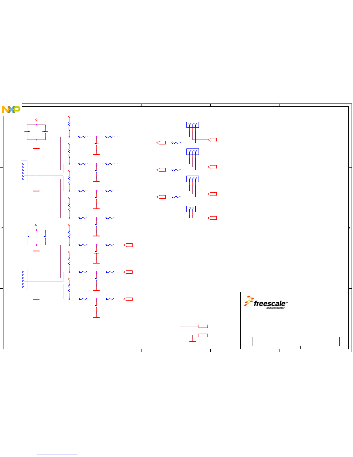
5
5
4
4
3
3
2
2
1
1
D D
C C
B B
A A
+5Vdc
+5Vdc
+5Vdc
PHASEA1
PHASEA0
PHASEB0
INDEX0
HOME0
PHASEB1
INDEX1
UNI3_BEMFZCA
UNI3_BEMFZCB
UNI3_BEMFZCC
+5Vdc
GND
+5Vdc
+5Vdc
GND
GND
GND
GND
GND
GND
GND
GND
GND
+5Vdc
+5Vdc
+5Vdc
+5Vdc
+5Vdc
+5Vdc
+5Vdc
GND
GND
GND
Drawing Title:
Size Document Number Rev
Date: Sheet of
Page Title:
ICAP Classification: FCP: FIUO: PUBI:
SCH-27475 PDF: SPF-27475 A
MPC5604P Controller Board
A4
Friday, January 27, 2012
ENCODERS
7 11
___ X
___
1. Maje 1009
75661, Roznov p.R., Czech Republic, Europe
Freescale Polovodice Ceska republika s.r.o.
Drawing Title:
Size Document Number Rev
Date: Sheet of
Page Title:
ICAP Classification: FCP: FIUO: PUBI:
SCH-27475 PDF: SPF-27475 A
MPC5604P Controller Board
A4
Friday, January 27, 2012
ENCODERS
7 11
___ X
___
1. Maje 1009
75661, Roznov p.R., Czech Republic, Europe
Freescale Polovodice Ceska republika s.r.o.
Drawing Title:
Size Document Number Rev
Date: Sheet of
Page Title:
ICAP Classification: FCP: FIUO: PUBI:
SCH-27475 PDF: SPF-27475 A
MPC5604P Controller Board
A4
Friday, January 27, 2012
ENCODERS
7 11
___ X
___
1. Maje 1009
75661, Roznov p.R., Czech Republic, Europe
Freescale Polovodice Ceska republika s.r.o.
R521
1.0K
R518
1.0K
R511
1.8K
R522
24
R507
1.8K
R509
24
R508
1.0K
R519
24
C503
47PF
C509
47PF
J502
HDR_1X3
123
R517
1.8K
C507
0.1UF
C504
47PF
C510
47PF
C506
2.2UF
R505
24JP500
HEADER 1X6
1
2
3
4
5
6
R502
1.8K
R514
1.8K
J501
HDR_1X3
123
R510
1.8K
R520
1.8K
C505
47PF
R512
1.0K
R523
1.8K
C508
47PF
R504
1.0K
C500
2.2UF
R501
24
C502
47PF R503
1.8K
J503
HDR 1X2 TH
1
2
R513
24
C501
0.1UF
JP501
HEADER 1X6
1
2
3
4
5
6
R500
1.0K
R515
1.0K
R506
1.8K
R516
24
J500
HDR_1X3
123
Page 37
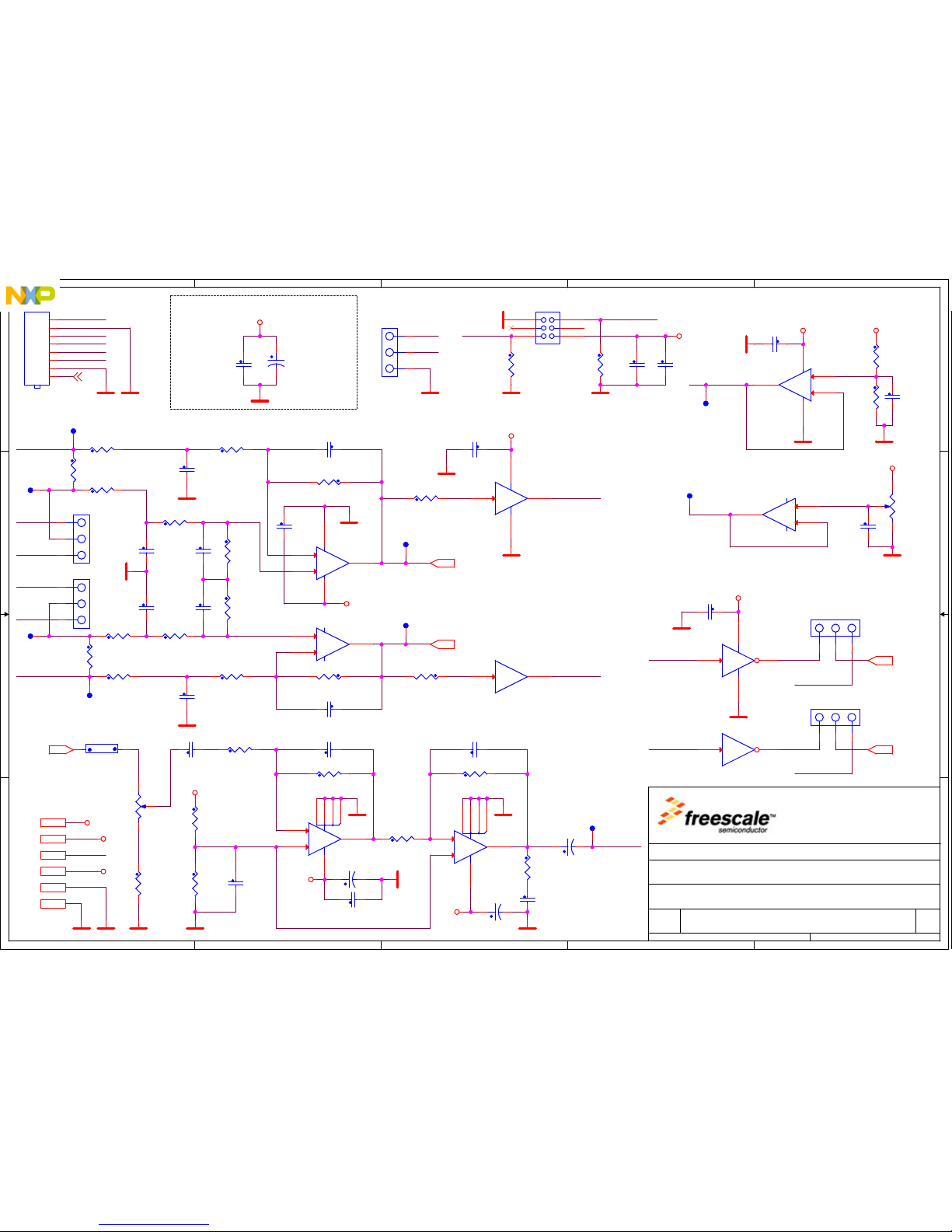
5
5
4
4
3
3
2
2
1
1
D D
C C
B B
A A
Mount close to Resolver Connector
SIN
REFSIN
COS
REFCOS
RES_GEN
VREFMID_BUF
RES_GEN
R_PHASE_A2
R_PHASE_B2
R_PHASE_A1
R_PHASE_B1
R_PHASE_A2
R_PHASE_B2
SIN
COS
REFCOS
OFFSET
OFFSET
REFSIN
OFFSET
COS
SIN
R_PHASE_A1
R_PHASE_B1
+3.3VA
+12V
+5VA
VREFMID_BUF
RES_REF
POS_SIN
POS_COS
PHASE_A
PHASE_B
+3.3VA
GNDP
V_sup
GNDA
Vref
+5VA
+3.3VA
+12V
+12V
+12V
GNDP GNDP GNDP
GNDA
GNDPGNDA
GNDA
GNDA
GNDA
GNDP GNDP
GNDA
+5VA
GNDP
GNDA
GNDA
+3.3VA
GNDP
GNDP
+3.3VA
GNDA
+3.3VA
GNDA GNDA GNDA
GNDA
+5VA
GNDPGNDA
Vref
GNDA
+3.3VA Vref
GNDAGNDA
+12V
+3.3VA
+5VA
Drawing Title:
Size Document Number Rev
Date: Sheet of
Page Title:
ICAP Classification: FCP: FIUO: PUBI:
SCH-27475 PDF: SPF-27475 A
MPC5604P Controller Board
A4
Friday, January 27, 2012
SinCos Interface
8 11
___ X
___
1. Maje 1009
75661, Roznov p.R., Czech Republic, Europe
Freescale Polovodice Ceska republika s.r.o.
Drawing Title:
Size Document Number Rev
Date: Sheet of
Page Title:
ICAP Classification: FCP: FIUO: PUBI:
SCH-27475 PDF: SPF-27475 A
MPC5604P Controller Board
A4
Friday, January 27, 2012
SinCos Interface
8 11
___ X
___
1. Maje 1009
75661, Roznov p.R., Czech Republic, Europe
Freescale Polovodice Ceska republika s.r.o.
Drawing Title:
Size Document Number Rev
Date: Sheet of
Page Title:
ICAP Classification: FCP: FIUO: PUBI:
SCH-27475 PDF: SPF-27475 A
MPC5604P Controller Board
A4
Friday, January 27, 2012
SinCos Interface
8 11
___ X
___
1. Maje 1009
75661, Roznov p.R., Czech Republic, Europe
Freescale Polovodice Ceska republika s.r.o.
C206
82PF
C227
0.1UF
U201A
NL27WZ17
1
52
6
TP16
C213
220PF
R203
10.0K
R218
3.90K
C222
3300PF
C209
0.1UF
+
C201
33UF
C224
0.1UF
R217
6.04K
+
C223
10UF
TP10
R209
10K
1 3
2
C202
0.1UF
R226
10.0K
R227
8.2K
TP13
-
+
U204B
TCA0372DWG
8
7
1
4512
13
2
R231
1.8K
+
-
U202A
MC33502DG
3
2
1
8 4
R210
6.04K
R219
47K
C226
0.1UF
C210
0.22UF
R220
47K
U203B
NL27WZ04
3 4
R212
6.04K
J204
HDR_1X3
1
2
3
C220
3300PF
R229
8.2K
R202
12.1K
R200
10.0K
R214
1.0K
R221
10K
13
2
TP8
U201B
NL27WZ17
3 4
C215
0.1UF
R201
12.1K
+
-
U200A
MC33502DG
3
2
1
84
TP11
C214
82PF
J207
HDR 1X8
1
2
3
4
5
6
7
8
C208
220PF
R223
2.7K
C218
220PF
C203
0.1UF
TP14
R206
1.0K
C219
82PF
J202
HDR_1X3
1
2
3
C221
0.22UF
C205
0.022UF
R215
100
R228
8.2K
R205
1.8K
R222
10.0K
C204
1.0UF
C212
82PF
R211
100
+
C225
22UF
R232
1.8K
+
-
U202B
MC33502DG
5
6
7
-
+
U204A
TCA0372DWG
9
10
1
4512
13
16
TP9
C200
0.1UF
J205
HDR_1X3
123
TP12
JP200
1 2
R208
6.04K
R230
8.2K
R207
1.8K
C207
0.1UF
R224
27
TP15
J201
HDR 2X3
1 2
3 4
65
J206
HDR_1X3
123
C211
220PF
U203A
NL27WZ04
1
52
6
+
C228
22UF
R225
10.0K
+
-
U200B
MC33502DG
5
6
7
J203
HDR_1X3
1
2
3
Page 38
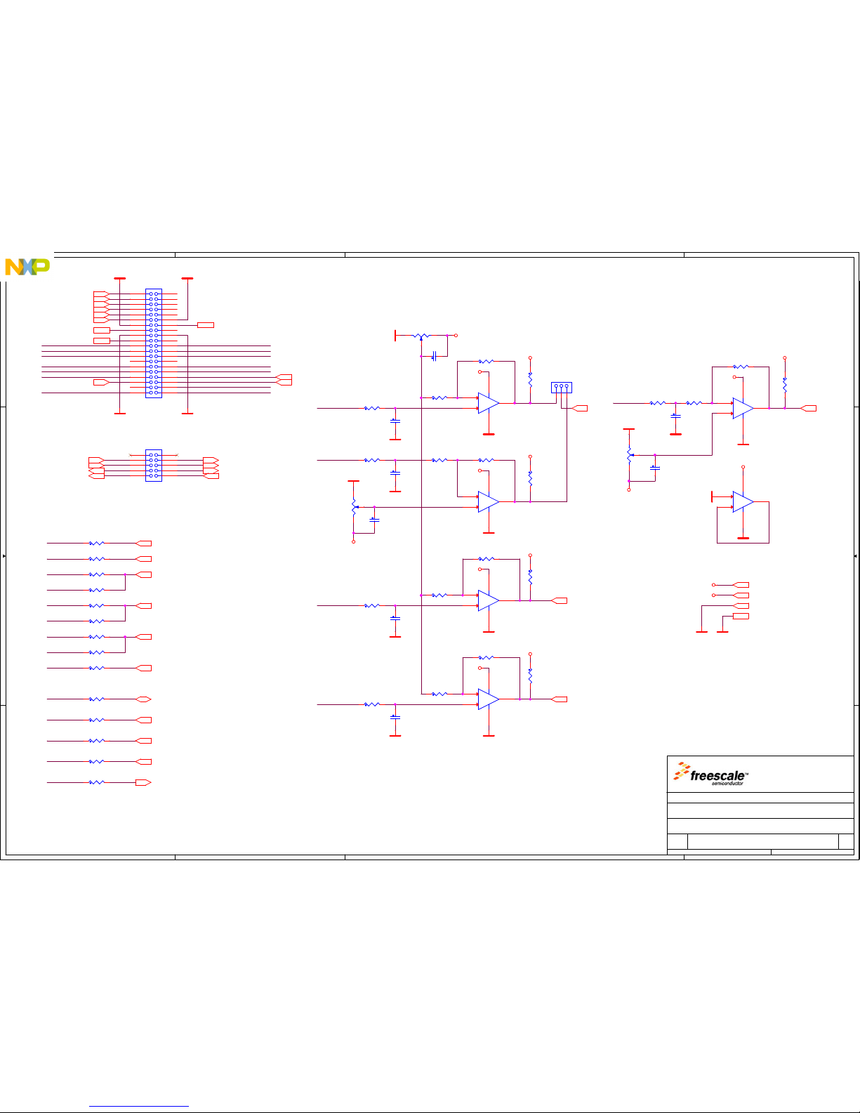
5
5
4
4
3
3
2
2
1
1
D D
C C
B B
A A
Either R320, R324 & R326 or R318, R322 & R325 are
used, depending on the required functionality
Control connector for MC33937 FET driver.
For BLDC applications do not populate R318, R322 & R325 .
For PMSM applications do not populate R320, R324 & R326.
UNI-3 DCBV
UNI-3 DCBI
UNI-3 PHAIS
UNI-3 DCBV
UNI-3 TEMP
UNI-3 PHAIS
UNI-3 BEMFA
UNI-3 BEMFCUNI-3 BEMFB
UNI-3 BEMFA
UNI-3 PHBIS
UNI-3 BEMFB
UNI-3 PHCIS
UNI-3 BEMFC
UNI-3 DCBV UNI-3 DCBI
UNI-3 SERIAL
UNI-3 PHAIS
UNI-3 BRAKE
UNI-3 DCBI
UNI-3 PFC
UNI-3 PHCIS
UNI-3 PFCEN
UNI-3 PFCZC
UNI-3 PHBIS
UNI-3 TEMP
UNI-3 BRAKE
UNI-3 PFC
UNI-3 PFCZC
UNI-3 SERIAL
UNI-3 PFCEN
UNI-3 PHBIS
UNI-3 PHCIS
PWM0
PWM1
PWM2
PWM3
PWM4
PWM5
FAULTB0FAULTB1
FAULTB2
FAULTB3
DCBV
DCBI
PHAIS
PHBIS
PHCIS
TEMP
SERIAL
UNI3_BEMFZCA
UNI3_BEMFZCCUNI3_BEMFZCB
UNI-3 +5V
UNI-3 +5V
UNI-3 +15VA
GND
+5Vdc
+3.3Vdc
GNDA
BRAKE
PFC
PFC_EN
PFC_ZC
33937_SIN33937_CS
33937_SOUT 33937_SCK
33937_OC
33937_INT
33937_EN
33937_/RST
+3.3Vdc
+5Vdc
+5Vdc
+3.3Vdc
+5Vdc
+3.3Vdc
+3.3Vdc
+5Vdc
+3.3Vdc
+5Vdc
+5Vdc
+5Vdc
+5Vdc
+5Vdc
GND GND
GNDA GNDA
GND
GND
GND
GND
GND
GND
GND
GND
GND
GND
GND
GND
GND
GND
GND
GND GNDA
+5Vdc
+3.3Vdc
Drawing Title:
Size Document Number Rev
Date: Sheet of
Page Title:
ICAP Classification: FCP: FIUO: PUBI:
SCH-27475 PDF: SPF-27475 A
MPC5604P Controller Board
A3
Friday, January 27, 2012
UNI3 Interface
9
11
___ X
___
1. Maje 1009
75661, Roznov p.R., Czech Republic, Europe
Freescale Polovodice Ceska republika s.r.o.
Drawing Title:
Size Document Number Rev
Date: Sheet of
Page Title:
ICAP Classification: FCP: FIUO: PUBI:
SCH-27475 PDF: SPF-27475 A
MPC5604P Controller Board
A3
Friday, January 27, 2012
UNI3 Interface
9
11
___ X
___
1. Maje 1009
75661, Roznov p.R., Czech Republic, Europe
Freescale Polovodice Ceska republika s.r.o.
Drawing Title:
Size Document Number Rev
Date: Sheet of
Page Title:
ICAP Classification: FCP: FIUO: PUBI:
SCH-27475 PDF: SPF-27475 A
MPC5604P Controller Board
A3
Friday, January 27, 2012
UNI3 Interface
9
11
___ X
___
1. Maje 1009
75661, Roznov p.R., Czech Republic, Europe
Freescale Polovodice Ceska republika s.r.o.
R321
22K
R326 0
J301
HDR_1X3
123
R332
15.0K
R336
1.8K
R334
0
C300
0.1UF
R333
1.8K
R307
15.0K
R308
15.0K
-
+
U300B
LM393M_NL
5
6
7
84
R330
1.8K
R323
15.0K
C305
0.1UF
R335
1.8K
R328 0
C303
0.1UF
R331
22K
-
+
U300A
LM393M_NL
3
2
1
84
J300
CON_2X20
1 2
3 4
65
7 8
9 10
11 12
13 14
15 16
17 18
19 20
21 22
23 24
25 26
27 28
29 30
31 32
33 34
35 36
37 38
39 40
C301
0.1UF
R316 0
R311
15.0K
C304
0.1UF
R313
22K
R329
22K
R305
22K
R310
15.0K
R306
15.0K
R303
22K
C307
0.1UF
R318 0 DNP
R317
1.5M
R327
1.5M
R315 0
R320 0
R324 0
C306
0.1UF
R300
10K
13
2
R302
1.0M
R319
22K
R322 0 DNP
-
+
U301A
LM393M_NL
3
2
1
84
-
+
U301B
LM393M_NL
5
6
7
84
R309
10K
1 3
2
R314
10K
1 3
2
R301
1.5M
C302
0.1UF
R304
22K
R312
1.0M
R325 0 DNP
-
+
U302B
LM393M_NL
5
6
7
84
-
+
U302A
LM393M_NL
3
2
1
84
J302
HDR 2X5
1 2
3 4
65
7 8
9 10
Page 39
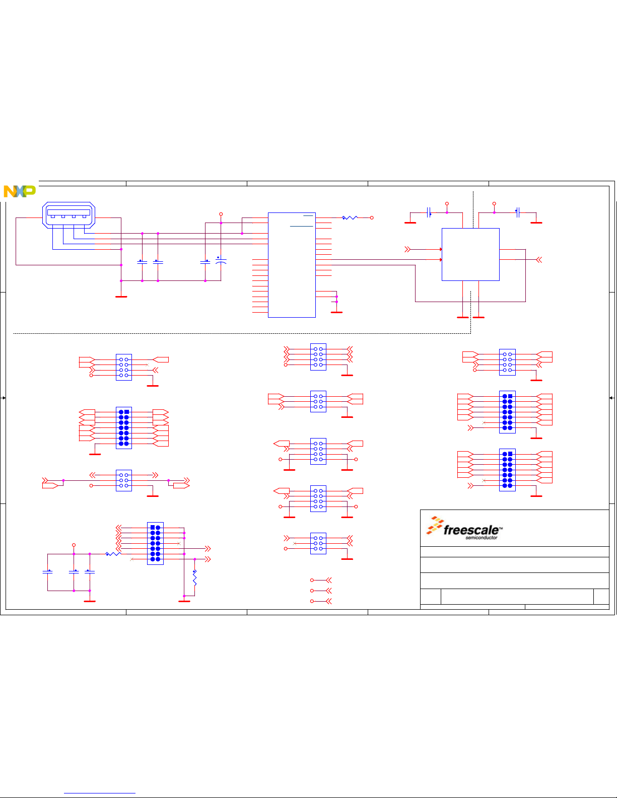
5
5
4
4
3
3
2
2
1
1
D D
C C
B B
A A
Place all headers & jumpers into 100mil raster
JTAG INTERFACE
Isolation Barrier
TOPBOTTOM
CAN_TX_PHY CAN_RX_PHY
SAFETY_CAN_TX_PHY SAFETY_CAN_RX_PHY
ANB_6ANB_7
ANB_8
ANB_0ANB_1
ANB_2ANB_3
ANB_4ANB_5
ANB_9
ANB_10
ANA_8
ANA_0ANA_1
ANA_2ANA_3
ANA_4ANA_5
ANA_6ANA_7
ANA_10
ANA_9
AN_12 AN_11
AN_14 AN_13
PWM_X2
PWM_X0PWM_X1
PWMA0PWMB0
PWMA1
PWMA2
PWMB1
PWMB2
FAULTB0
FAULTB2
FAULTB1
FAULTB3
PHASEB1
INDEX1
PHASEA0 PHASEB0
INDEX0 HOME0PHASEA1
SCI1_TXSCI1_RX
+3.3Vdc
+5Vdc
GND GND
MCU_3.3V
GNDA
GNDA
GNDGND
GNDGND
+3.3Vdc
+5Vdc
GND
GND
+3.3Vdc
GND
+3.3Vdc
GND
+3.3Vdc
GND
+3.3Vdc
GND
+3.3Vdc
GNDA
+3.3Vdc
+5Vdc
GNDB
VDD_USB
VDD_USB
VDD_USB
GNDB GND
MCU_3.3V
GNDGNDB
GNDB
MCU_3.3V
CAN_TX
CAN_RX
TDO
TDI
RESET
EVTI
TMS
JCOMP
TCK
SAFETY_CAN_TX
SAFETY_CAN_RX
GPIOA12 GPIOA1 3
SCI1_RX SCI1_TX
SPI3_SCK
SPI3_SIN
SCI0_TXSCI0_RX
SPI3_SOUT
SPI3_CS0
PWMA3
PWM_X3
PWMB3
+3.3VA2
+3.3VA2
+3.3VA2
+3.3Vdc
+5Vdc
ETO_4
ETO_5
PHASE_B PHASE_A
SCI0_TX
SCI0_RX
MCU_3.3V
Drawing Title:
Size Document Number Rev
Date: Sheet of
Page Title:
ICAP Classification: FCP: FIUO: PUBI:
SCH-27475 PDF: SPF-27475 A
MPC5604P Controller Board
A4
Friday, January 27, 2012
HEADERS
10 1 1
___ X
___
1. Maje 1009
75661, Roznov p.R., Czech Republic, Europe
Freescale Polovodice Ceska republika s.r.o.
Drawing Title:
Size Document Number Rev
Date: Sheet of
Page Title:
ICAP Classification: FCP: FIUO: PUBI:
SCH-27475 PDF: SPF-27475 A
MPC5604P Controller Board
A4
Friday, January 27, 2012
HEADERS
10 1 1
___ X
___
1. Maje 1009
75661, Roznov p.R., Czech Republic, Europe
Freescale Polovodice Ceska republika s.r.o.
Drawing Title:
Size Document Number Rev
Date: Sheet of
Page Title:
ICAP Classification: FCP: FIUO: PUBI:
SCH-27475 PDF: SPF-27475 A
MPC5604P Controller Board
A4
Friday, January 27, 2012
HEADERS
10 1 1
___ X
___
1. Maje 1009
75661, Roznov p.R., Czech Republic, Europe
Freescale Polovodice Ceska republika s.r.o.
U2
CP2102
REGIN
7
VDD
6
GND
3
VBUS
8
D-
5
D+
4
RST
9
SUSPEND
12
SUSPEND
11
RI
2
DCD
1
DTR
28
DSR
27
TXD
26
RTS
24
CTS
23
NC1
10
NC2
13
NC3
14
NC4
15
NC5
16
NC6
17
NC7
18
NC8
19
NC9
20
NC10
21
NC11
22
RXD
25
EPAD
29
C38
0.01UF
J6
HDR_2X4
12
34
6 5
78
C40
1.0UF
J3
HDR_2X4
12
34
6 5
78
J13
HDR_2X4
12
34
6 5
78
J4
HDR_2X7
12
34
56
78
910
1112
1314
C342
0.1 UF
R37
0
J14
HDR 2X3
12
34
6 5
C42
0.1 UF
C39
0.1 UF
VD-D+G
USB_TYPE_A
J311
S1
A1
A2
A3
A4
S2
R339
4.7K
R38
10.0K
C41
0.1 UF
J5
HDR_2X7
1 2
3 4
5 6
7 8
9 10
11 12
13 14
J15
HDR 2X3
12
34
6 5
+
C43
4.7UF
J11
HDR_2X4
12
34
6 5
78
C37
4.7UF
J7
HDR_2X7
12
34
56
78
910
1112
1314
C343
0.1 UF
J10
HDR_2X7
12
34
56
78
910
1112
1314
J8
HDR_2X4
12
34
6 5
78
J9
HDR 2X3
1 2
3 4
65
U12
ADUM1201
VDD11VDD2
8
VIA
7
VIB
3
VOA
2
VOB
6
GND14GND2
5
Page 40
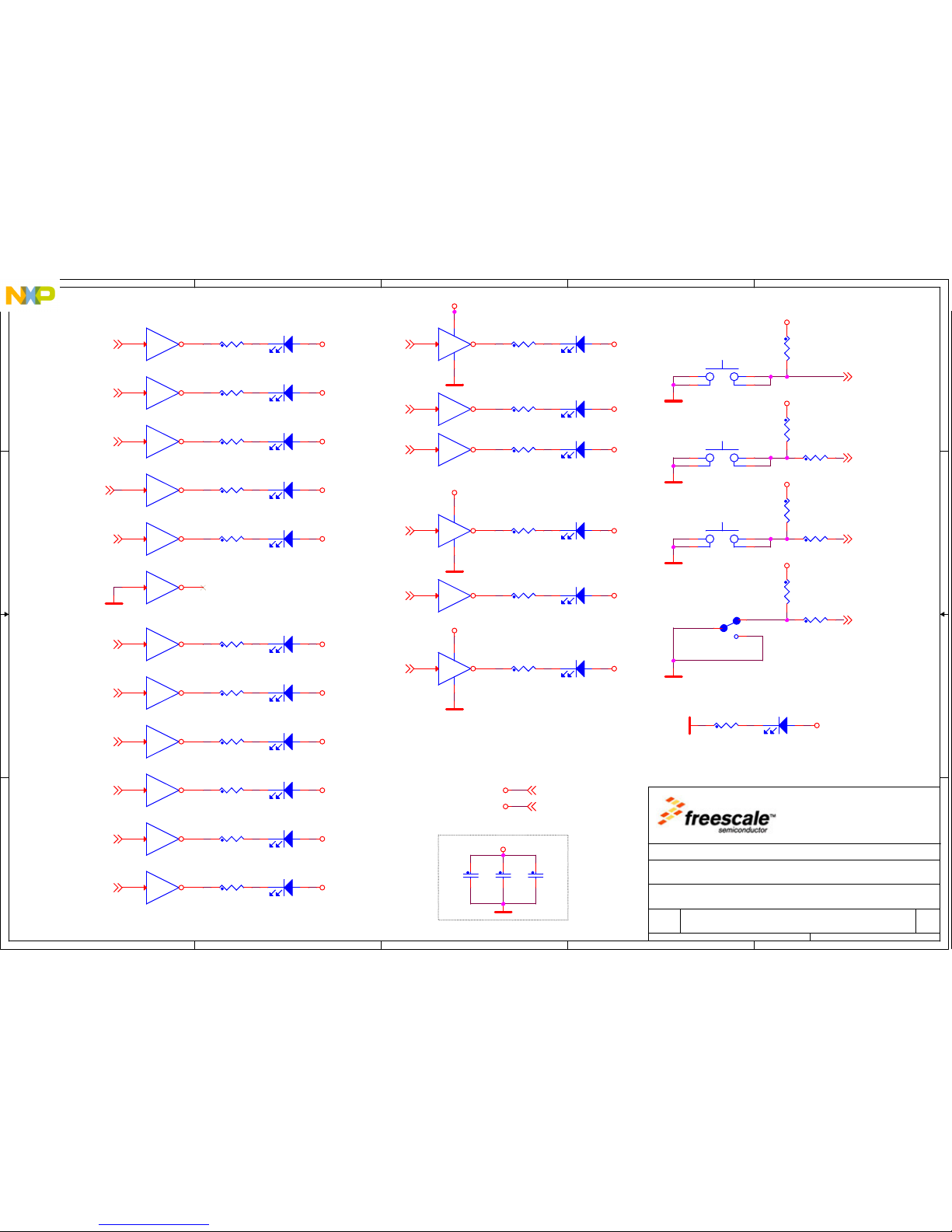
5
5
4
4
3
3
2
2
1
1
D D
C C
B B
A A
74HC
+3.3Vdc
+3.3Vdc
+3.3Vdc
+3.3Vdc
+3.3Vdc
+3.3Vdc
+3.3Vdc
+3.3Vdc
+3.3Vdc
+3.3Vdc
+3.3Vdc
+3.3Vdc
+3.3Vdc
+3.3Vdc
+3.3Vdc
+3.3Vdc
+3.3Vdc
+3.3Vdc
MCU_3.3V
MCU_3.3V
MCU_3.3V
MCU_3.3V
GND
GND
GND
GND
GND
GND
GND
GND
GND
+3.3Vdc
+3.3Vdc
+3.3Vdc
+3.3Vdc
MCU_3.3V
GND
+3.3Vdc
GPIOA12
PWMA0 PWMB0
PWMA1
PWMB1
PWMA2
PWMB2
FAULTB0
FAULTB1
FAULTB2
FAULTB3
EIRQ#6
EIRQ#7
PHASEA0
PHASEB0
INDEX0
PWMA3
PWMB3
RESET
ON/OFF
GPIOA13
+3.3Vdc
MCU_3.3V
Drawing Title:
Size Document Number Rev
Date: Sheet of
Page Title:
ICAP Classification: FCP: FIUO: PUBI:
SCH-27475 PDF: SPF-27475 A
MPC5604P Controller Board
A4
Friday, January 27, 2012
LEDs and Buttons
11 1 1
___ X
___
1. Maje 1009
75661, Roznov p.R., Czech Republic, Europe
Freescale Polovodice Ceska republika s.r.o.
Drawing Title:
Size Document Number Rev
Date: Sheet of
Page Title:
ICAP Classification: FCP: FIUO: PUBI:
SCH-27475 PDF: SPF-27475 A
MPC5604P Controller Board
A4
Friday, January 27, 2012
LEDs and Buttons
11 1 1
___ X
___
1. Maje 1009
75661, Roznov p.R., Czech Republic, Europe
Freescale Polovodice Ceska republika s.r.o.
Drawing Title:
Size Document Number Rev
Date: Sheet of
Page Title:
ICAP Classification: FCP: FIUO: PUBI:
SCH-27475 PDF: SPF-27475 A
MPC5604P Controller Board
A4
Friday, January 27, 2012
LEDs and Buttons
11 1 1
___ X
___
1. Maje 1009
75661, Roznov p.R., Czech Republic, Europe
Freescale Polovodice Ceska republika s.r.o.
SW1
B3S-1002
1
2
3
4
D17
HSMG-C170
AC
R44
270
D15
SML-LX0805YC-TR
AC
D12
HSMS-C170
AC
D11
HSMG-C170
AC
C145
0.1 UF
U4C
MC74HC04ADG
5 6
VCC
GND
U3A
MC74HC04ADG
1 2
147
R41
270
SW4
SPDT on-on 20V
1
3
2
VCC
GND
U11A
MC74HC04ADG
1 2
147
D4
HSMG-C170
AC
R64
270
D18
HSMG-C170
AC
U3B
MC74HC04ADG
3 4
D16
SML-LX0805YC-TR
AC
U11F
MC74HC04ADG
13 12
D8
HSMS-C170
AC
R62
270
D1
SML-LX0805YC-TR
AC
R59
270
U3C
MC74HC04ADG
5 6
D14
HSMG-C170
AC
U4B
MC74HC04ADG
3 4
R63
270
D5
SML-LX0805YC-TR
AC
R61
270
VCC
GND
U4A
MC74HC04ADG
1 2
147
R55
4.7K
U11E
MC74HC04ADG
11 10
R58
270
R51
4.7K
R53
270
D9
HSMS-C170
AC
R45
4.7K
R48
1.8K
U4F
MC74HC04ADG
13 12
R42
4.7K
R52
1.8K
R49
270
U4D
MC74HC04ADG
9 8
U3D
MC74HC04ADG
9 8
R57
1.8K
D2
HSMG-C170
AC
R46
270
U3E
MC74HC04ADG
11 10
D6
HSMG-C170
AC
U11B
MC74HC04ADG
3 4
SW3
B3S-1002
1
2
3
4
R43
270
D7
HSMS-C170
AC
D13
HSMS-C170
AC
R60
270
D10
HSMS-C170
AC
C144
0.1 UF
R40
270
U4E
MC74HC04ADG
11 10
U11C
MC74HC04ADG
5 6
U3F
MC74HC04ADG
13 12
R56
270
SW2
B3S-1002
1
2
3
4
D3
SML-LX0805YC-TR
AC
R54
270
U11D
MC74HC04ADG
9 8
R50
270
R47
270
C146
0.1 UF
Page 41

References
8 References
The MPC5604P documentation is available at the web site, http://www.freescale.com. as follows:
• Reference manuals — MPC5604P modules in detail
• Data sheets — information mainly on the device’s AC, DC, thermal characteristics and packages
pin-out
• Product briefs — device overview
• Application notes — address specific design issues
MPC5604P Controller Board User’s Guide, Rev. 0
Freescale30
Page 42

THIS PAGE IS INTENTIONALLY BLANK
MPC5604P Controller Board User’s Guide, Rev. 0
Freescale 31
Page 43

How to Reach Us:
Home Page:
www.freescale.com
Web Support:
http://www.freescale.com/support
USA/Europe or Locations Not Listed:
Freescale Semiconductor, Inc.
Technical Information Center, EL516
2100 East Elliot Road
Tempe, Arizona 85284
+1-800-521-6274 or +1-480-768-2130
www.freescale.com/support
Europe, Middle East, and Africa:
Freescale Halbleiter Deutschland GmbH
Technical Information Center
Schatzbogen 7
81829 Muenchen, Germany
+44 1296 380 456 (English)
+46 8 52200080 (English)
+49 89 92103 559 (German)
+33 1 69 35 48 48 (French)
www.freescale.com/support
Japan:
Freescale Semiconductor Japan Ltd.
Headquarters
ARCO Tower 15F
1-8-1, Shimo-Meguro, Meguro-ku,
Tokyo 153-0064
Japan
0120 191014 or +81 3 5437 9125
[email protected]
Asia/Pacific:
Freescale Semiconductor China Ltd.
Exchange Building 23F
No. 118 Jianguo Road
Chaoyang District
Beijing 100022
China
+86 10 5879 8000
[email protected]
For Literature Requests Only:
Freescale Semiconductor Literature Distribution Center
1-800-441-2447 or 303-675-2140
Fax: 303-675-2150
[email protected]
Information in this document is provided solely to enable system and software
implementers to use Freescale products. There are no express or implied copyright
licenses granted hereunder to design or fabricate any integrated circuits or integrated
circuits based on the information in this document.
Freescale reserves the right to make changes without further notice to any products
herein. Freescale makes no warranty, representation or guarantee regarding the
suitability of its products for any particular purpose, nor does Freescale assume any
liability arising out of the application or use of any product or circuit, and specifically
disclaims any and all liability, including without limitation consequential or incidental
damages. “Typical” parameters that may be provided in Freescale data sheets and/or
specifications can and do vary in different applications and actual performance may vary
over time. All operating parameters, including “Typicals”, must be validated for each
customer application by customer’s technical experts. Freescale does not convey any
license under its patent rights nor the rights of others. Freescale products are not
designed, intended, or authorized for use as components in systems intended for
surgical implant into the body, or other applications intended to support or sustain life,
or for any other application in which the failure of the Freescale product could create a
situation where personal injury or death may occur. Should Buyer purchase or use
Freescale products for any such unintended or unauthorized application, Buyer shall
indemnify and hold Freescale and its officers, employees, subsidiaries, affiliates, and
distributors harmless against all claims, costs, damages, and expenses, and
reasonable attorney fees arising out of, directly or indirectly, any claim of personal injury
or death associated with such unintended or unauthorized use, even if such claim
alleges that Freescale was negligent regarding the design or manufacture of the part.
For information on Freescale’s Environmental Products program, go to
http://www.freescale.com/epp.
Freescale™ and the Freescale logo are trademarks of Freescale, Inc. All other product
or service names are the property of their respective owners.
The Power Architecture and Power.org word marks and the Power and Power.org logos
and related marks are trademarks and service marks licensed by Power.org
© Freescale, Inc. 2012. All rights reserved.
Document Number: MPC5604PUG
Rev. 0
07/2012
 Loading...