

Page 1

Freescale Semiconductor
MPC5510 Reference Manual
MPC5510RM
Rev. 1.1, 04/2012
This is the MPC5510 Reference Manual set consisting of the following files:
• MPC5510 Reference Manual Addendum, Rev 1
• MPC5510 Reference Manual, Rev 1
© Freescale Semiconductor, Inc., 2012. All rights reserved.
Page 2

Freescale Semiconductor
Reference Manual Addendum
MPC5510 Reference Manual
Addendum
MPC5510RMAD
Rev. 1, 04/2012
This addendum document describes corrections to the
MPC5510 Microcontroller Reference Manual, order
number MPC5510RM. For convenience, the addenda
items are grouped by revision. Please check our website
at http://www.freescale.com/powerarchitecture for the
latest updates.
The current version available of the MPC5510
Microcontroller Reference Manual is Revision 1.0.
Table of Contents
1 Addendum for Revision 1.0. . . . . . . . . . . . . . . . . . 2
2 Revision History . . . . . . . . . . . . . . . . . . . . . . . . . . 5
© Freescale Semiconductor, Inc., 2012. All rights reserved.
Page 3

Addendum for Revision 1.0
1 Addendum for Revision 1.0
Table 1. MPC5510RM Rev 1.0 Addendum
Location Description
Section 2.2
“Signal Properties
Summary”
Section 3.3
“System Clock
Architecture Block
Diagram”
Added a note just above “MPC5510 Signal Properties” table:
“Please note that analog input pins (ANx) are directly connected to the eQADC and that they are not routed
through the PCRx register; thus, changes in the PCR register does not affect these inputs.”
Updated the paragraph:
To optimize system power consumption, the MPC5510 supports system-level clock dividers, static clock
gating using peripheral-level module disable (MDIS) bits and a system-level halt mechanism. Figure 3-2
shows the device-level clock gating mechanism for the MPC5510. Figure 3-3 shows a more detailed
implementation of the MDIS and halt mechanism connections for a given peripheral. These features are
detailed in subsequent sections.
Added a new NOTE:
While combining DMA with peripheral modules (for example eSCI), the user has to use LPCLKDIVx = 0
(no divide) to ensure that the DMA.DONE (same as DMA ACK) is correctly acknowledged by the
peripheral. Otherwise, DMA.DONE may not be sampled correctly , leading to data loss. In the case of eSCI
peripheral, BERR flag will be set and the peripheral behavior will be unexpected if LPCLKDIV4 > 0.
MPC5510 Reference Manual Addendum, Rev. 1
Freescale Semiconductor2
Page 4

Table 1. MPC5510RM Rev 1.0 Addendum
Protocol clock
Oscillator clock
Module clock
MCKO
MCKO
divider
CLK_SRC
MDIS
FlexRAY
Protocol clock
CLK_SRC
MDIS
FlexCAN_A
LPCLKDIV0
MDIS
DSPI_A
MDIS
ESCI_A,IIC_A,PIT
(RTI)
Protocol clock
CLK_SRC
MDIS
FlexCAN_B-F
LPCLKDIV2
CLKOUT
CLKOUT
divider
MDIS
DSPI_B-D
MDIS
ESCI_B-H
MDIS
eMIOS
MDIS
MLB
Cores INTC, DMA, SIU, RAM
Flash, BAM, AIPS, AXBS,
LPCLKDIV3
LPCLKDIV4
LPCLKDIV5
LPCLKDIV6
LPCLKDIV1
Switcher
and
divider
Nexus
EBI
NPC
Module clock
DIV/2
PLL
IRC
XOSC
Bypass clock
System clock
Module clock
MCM, eQADC
Location Description
Addendum for Revision 1.0
Architecture Block
Section 3.3
“System Clock
Diagram”
Updated Figure 3-2 ”System Clock Architecture”.
MPC5510 Reference Manual Addendum, Rev. 1
Freescale Semiconductor 3
Page 5

Addendum for Revision 1.0
Table 6-27: LPCLKDIV Module Groups
LPCLKDIVn Modules
LPCLKDIV0 FlexCAN_A, DSPI_A
LPCLKDIV1 ESCI_A, I
2
C_A, PIT
LPCLKDIV2 FlexCAN_B-F
LPCLKDIV3 DSPI_B-D
LPCLKDIV4 ESCI_B-H
LPCLKDIV5 eMIOS
LPCLKDIV6 MLB
LPCLKDIV7 Reserved
Table 1. MPC5510RM Rev 1.0 Addendum
Location Description
Section 3.5.2
“Halt Clock Gating”
Section 5.3.2
”Low-power Mode
Entry”
Section 6.3.2.2
“Reset Status
Register
(SIU_RSR)”
Section 6.3.2.25
“System Clock
Register
(SIU_SYSCLK)”
Added a note:
SIU_HLT is not delayed by any pending interrupt for specific modules to be serviced. If any interrupt is
raised after the SIU_HLT request, it may cause the interrupt to hang. To avoid this, it is advised that all
interrupts are disabled before entering the SIU_HLT state and then, re-enabled once SIU_HLT is exited.
The result is that any interrupt will be flagged, but not triggered within its specific interrupt service routine.
Once the SIU_HLT has been enabled, any pending interrupt will be taken as normal. In the case of STOP
mode exit, an external interrupt may be required. In this case, the specific exit interrupt may be enabled,
but software must ensure the interrupt does not occur simultaneously with SIU_HLT being enabled.
Updated “The system clock source should be set to the 16 MHz IRC prior to ... ” to “The system cloc k source
needs be set to the 16 MHz IRC (with the default divide by 1 system clock configuration) prior to ...”.
Updated point 1. The updated text is as follows:
“If any reset request has negated and the device is still in the resulting reset, and then an external reset is
requested, both the original reset type and external reset status bits will be set. In this case, the device
started the reset sequence due to a non-external reset request but ended the reset sequence after an
external reset request.”
Updated figure note 3 of Figure 6-3, “Reset Status Register (SIU_RSR”. The updated text is as follows:
“The ERS bit is also set if the RESET pin is held low to extend the reset sequence.”
Aligned table 6-27 “LPCLKDIV Module Groups”, as mentioned below.
Section 24.1.1
“Block Diagram”
Section 24.3.2.3
“eSCI Data
Register
(ESCIx_DR)”
Added a figure note for peripheral clock in the “eSCI
Refer to Section 3.3, “ System Clock Architecture Block Diagram”.
Added a note:
eSCI transmission delay will depend on the actual Tx load into the Data Register referenced with the
internal clock, if the load occurs before 45% of a bit time has passed, the Tx load will be transmitted in less
than a bit time. Otherwise, the Tx will take up to 1.5 of a bit time.
MPC5510 Reference Manual Addendum, Rev. 1
Block Diagram” figure:
Freescale Semiconductor4
Page 6

Table 1. MPC5510RM Rev 1.0 Addendum
Location Description
Revision History
Section 31.4.3.3
”External Trigger
Input Multiplexing”
• Updated the title from “External Trigger from eTPU to eMIOS Channels“ to “External Trigger Input
Multiplexing”.
• Updated the text of this section to:
The four eQADC external trigger inputs can be connected to two different external pins or one of two PIT
channels. The input source for each eQADC external trigger is individually specified in the IMUX Select
Register 0 (SIU_ISEL0). Figure 6-50 gives an example of the multiplexing of an eQADC external trigger
input. As shown in the figure, the ETRIG[0] input of the eQADC can be connected to the PC4 pin, the PG4
pin, the PIT7 channel, or the PIT8 channel. Remaining ETRIG inputs are multiplexed in the same manner.
The eQADC trigger numbers specified by SIU_ETISR[TSEL(0-3)] correspond to CFIFO numbers 0-3. To
calculate the CFIFO number that each trigger is connected to, divide the eDMA channel number by 2.
2 Revision History
Table 2 provides a revision history for this document.
Table 2. Revision History Table
Rev. Number Substantive Changes Date of Release
1.0 First release. 04/2012
MPC5510 Reference Manual Addendum, Rev. 1
Freescale Semiconductor 5
Page 7

How to Reach Us:
Home Page:
www.freescale.com
Web Support:
http://www.freescale.com/support
USA/Europe or Locations Not Listed:
Freescale Semiconductor, Inc.
Technical Information Center, EL516
2100 East Elliot Road
Tempe, Arizona 85284
+1-800-521-6274 or +1-480-768-2130
www.freescale.com/support
Europe, Middle East, and Africa:
Freescale Halbleiter Deutschland GmbH
Technical Information Center
Schatzbogen 7
81829 Muenchen, Germany
+44 1296 380 456 (English)
+46 8 52200080 (English)
+49 89 92103 559 (German)
+33 1 69 35 48 48 (French)
www.freescale.com/support
Japan:
Freescale Semiconductor Japan Ltd.
Headquarters
ARCO Tower 15F
1-8-1, Shimo-Meguro, Meguro-ku,
Tokyo 153-0064
Japan
0120 191014 or +81 3 5437 9125
[email protected]
Asia/Pacific:
Freescale Semiconductor China Ltd.
Exchange Building 23F
No. 118 Jianguo Road
Chaoyang District
Beijing 100022
China
+86 10 5879 8000
[email protected]
For Literature Requests Only:
Freescale Semiconductor Literature Distribution Center
1-800-441-2447 or 303-675-2140
Fax: 303-675-2150
[email protected]
Information in this document is provided solely to enable system and
software implementers to use F reescale S emiconductor prod ucts. There ar e
no express or implied copyright licenses granted hereunder to design or
fabricate any integrated circuits or integrated circuits based on the
information in this document.
Freescale Semiconducto r reserves the right to mak e changes without further
notice to any products herein. F reescale Se miconductor m akes no w arranty,
representation or guarantee regarding the suitability of its products for any
particular purpose, nor does Freescale Semiconductor assume any liability
arising out of the application or use of any produ ct or circuit, an d specific ally
disclaims any and all liability, including without limitation consequential or
incidental damages. “Typical” param eters that ma y be pro vided in F r eescale
Semiconductor data sheets and/or speci fications can and do v ary in differ ent
applications and actual performance may vary over time. All operating
parameters, including “Typicals”, must be validated for each customer
application by customer’s technical experts. Freescale Semiconductor does
not convey any license under its patent rights nor the rights of others.
Freescale Semicondu ctor products are not de signed, intended, or authorized
for use as components in systems intended for surgical implant into the body ,
or other applications intended to support or sustain life, or for any other
application in which the failure of the Freescale Semiconductor product could
create a situation where personal injury or death may occur. Should Buyer
purchase or use Freescal e Semiconductor products f or an y such unintended
or unauthorized application, B uyer sha ll indemnify and hold Freescale
Semiconductor and its officers, employees, subsidiaries, affiliates, and
distributors harmless against all claims, costs, damages, and expenses, and
reasonable attorney fees arising out of, directly or indirectly, any claim of
personal injury or death associated with such unintended or unauthorized
use, even if such claim alleges that Freescale Semiconductor was negligent
regarding the design or manufacture of the part.
Freescale™ and the Freescale logo are trademarks of Freescale
Semiconductor, Inc. All other product or service names are the propert y
of their respective owners.© Freescale Semiconductor, Inc. 2012. All rights
reserved.
MPC5510RMAD
Rev. 1
04/2012
Page 8

MPC5510 Microcontroller Family
Reference Manual
Devices Supported:
MPC5517G/E/S
MPC5516G/E/S
MPC5515S
MPC5514G/E
Document Number: MPC5510RM
Rev. 1
06/2008
PRELIMINARY
Page 9

How to Reach Us:
Home Page:
www.freescale.com
Web Support:
http://www.freescale.com/support
USA/Europe or Locations Not Listed:
Freescale Semiconductor, Inc.
Technical Information Center, EL516
2100 East Elliot Road
Tempe, Arizona 85284
1-800-521-6274 or +1-480-768-2130
www.freescale.com/support
Europe, Middle East, and Africa:
Freescale Halbleiter Deutschland GmbH
Technical Information Center
Schatzbogen 7
81829 Muenchen, Germany
+44 1296 380 456 (English)
+46 8 52200080 (English)
+49 89 92103 559 (German)
+33 1 69 35 48 48 (French)
www.freescale.com/support
Japan:
Freescale Semiconductor Japan Ltd.
Headquarters
ARCO Tower 15F
1-8-1, Shimo-Meguro, Meguro-ku,
Tokyo 153-0064
Japan
0120 191014 or +81 3 5437 9125
[email protected]
Asia/Pacific:
Freescale Semiconductor China Ltd.
Exchange Building 23F
No. 118 Jianguo Road
Chaoyang District
Beijing 100022
China
+86 10 5879 8000
[email protected]
For Literature Requests Only:
Freescale Semiconductor Literature Distribution Center
P.O. Box 5405
Denver, Colorado 80217
1-800-441-2447 or +1-303-675-2140
Fax: +1-303-675-2150
[email protected]
Information in this document is provided solely to enable system and
software implementers to use F reescale Se miconductor products . There are
no express or implied copyright licenses granted hereunder to design or
fabricate any integrated circ uits or in te g rated circuits based on the
information in this document.
Freescale Semiconductor reserves the right to mak e changes without further
notice to any products herein. F reescale Semico nductor mak es no warr anty,
representation or guarantee regarding the suitability of its products for any
particular purpose, nor does Freescale Semiconductor assume any liability
arising out of the application or use of any product or circuit, an d specif ically
disclaims any and all liability, including without limitation consequential or
incidental damages. “Typical” parameters that may be provided in Freescale
Semiconductor data sheets and/or spec ifications can and d o vary in diff erent
applications and actual performance may vary over time. All operating
parameters, including “Typicals”, must be validated for each customer
application by customer’s technical experts. Freescale Semiconductor does
not convey any license under its patent rights nor the rights of others.
Freescale Semiconduct or products are not des igned, intended, or a uthorized
for use as components in systems intended for surgical implant into the bo dy ,
or other applications intended to support or sustain life, or for any other
application in which the failure of the Freescale Semiconductor product could
create a situation where personal injury or death may occur. Should Buyer
purchase or use Freescale Semiconductor products for any such unintended
or unauthorized application, Buyer shall indemnify and hold Freescale
Semiconductor and its officers, employees, subsidiaries, affiliates, and
distributors harmless against all claims, costs , damages, and exp enses, and
reasonable attorney fees arising out of, directly or indirectly, any claim of
personal injury or death associated with such unintended or unauthorized
use, even if such claim al leges th at Freescale Semiconductor was negligent
regarding the design or manufacture of the part.
Freescale™ and the Freescale logo are trademarks of Freescale
Semiconductor, Inc. The Power Architecture and Power.org word marks and
the Power and P owe r .org logos and r elated marks are trade marks and service
marks licensed by Power.org.
All other product or service names are the property of their respective o wners .
© Freescale Semiconductor, Inc. 2007, 2008. All rights reserved.
MPC5510RM
Rev. 1
06/2008
Page 10

Chapter 1
Overview
1.1 Introduction . . . . . . . . . . . . . . . . . . . . . . . . . . . . . . . . . . . . . . . . . . . . . . . . . . . . . . . . . . . . . . 1-1
1.2 Block Diagram . . . . . . . . . . . . . . . . . . . . . . . . . . . . . . . . . . . . . . . . . . . . . . . . . . . . . . . . . . . . 1-2
1.3 MPC5510 Family Comparison . . . . . . . . . . . . . . . . . . . . . . . . . . . . . . . . . . . . . . . . . . . . . . . . 1-3
1.3.1 Family Feature Set Scaling . . . . . . . . . . . . . . . . . . . . . . . . . . . . . . . . . . . . . . . . . . . 1-5
1.4 Chip-Level Features . . . . . . . . . . . . . . . . . . . . . . . . . . . . . . . . . . . . . . . . . . . . . . . . . . . . . . . . 1-6
1.5 Low-Power Operation . . . . . . . . . . . . . . . . . . . . . . . . . . . . . . . . . . . . . . . . . . . . . . . . . . . . . . 1-7
1.6 Memory Map . . . . . . . . . . . . . . . . . . . . . . . . . . . . . . . . . . . . . . . . . . . . . . . . . . . . . . . . . . . . . 1-7
Chapter 2
Signal Descriptions
2.1 Introduction . . . . . . . . . . . . . . . . . . . . . . . . . . . . . . . . . . . . . . . . . . . . . . . . . . . . . . . . . . . . . . 2-1
2.2 Signal Properties Summary . . . . . . . . . . . . . . . . . . . . . . . . . . . . . . . . . . . . . . . . . . . . . . . . . . 2-1
2.3 Power and Ground Supply Summary . . . . . . . . . . . . . . . . . . . . . . . . . . . . . . . . . . . . . . . . . . 2-12
2.4 Pinout – 144 LQFP . . . . . . . . . . . . . . . . . . . . . . . . . . . . . . . . . . . . . . . . . . . . . . . . . . . . . . . . 2-14
2.5 Pinout – 176 LQFP . . . . . . . . . . . . . . . . . . . . . . . . . . . . . . . . . . . . . . . . . . . . . . . . . . . . . . . . 2-15
2.6 Pinout – 208 BGA . . . . . . . . . . . . . . . . . . . . . . . . . . . . . . . . . . . . . . . . . . . . . . . . . . . . . . . . 2-16
2.7 Detailed External Signal Descriptions . . . . . . . . . . . . . . . . . . . . . . . . . . . . . . . . . . . . . . . . . 2-16
2.7.1 Port A Pins . . . . . . . . . . . . . . . . . . . . . . . . . . . . . . . . . . . . . . . . . . . . . . . . . . . . . . . 2-16
2.7.2 Port B Pins . . . . . . . . . . . . . . . . . . . . . . . . . . . . . . . . . . . . . . . . . . . . . . . . . . . . . . . 2-17
2.7.3 Port C Pins . . . . . . . . . . . . . . . . . . . . . . . . . . . . . . . . . . . . . . . . . . . . . . . . . . . . . . . 2-19
2.7.4 Port D Pins . . . . . . . . . . . . . . . . . . . . . . . . . . . . . . . . . . . . . . . . . . . . . . . . . . . . . . . 2-21
2.7.5 Port E Pins . . . . . . . . . . . . . . . . . . . . . . . . . . . . . . . . . . . . . . . . . . . . . . . . . . . . . . . 2-24
2.7.6 Port F Pins . . . . . . . . . . . . . . . . . . . . . . . . . . . . . . . . . . . . . . . . . . . . . . . . . . . . . . . 2-25
2.7.7 Port G Pins . . . . . . . . . . . . . . . . . . . . . . . . . . . . . . . . . . . . . . . . . . . . . . . . . . . . . . . 2-28
2.7.8 Port H Pins . . . . . . . . . . . . . . . . . . . . . . . . . . . . . . . . . . . . . . . . . . . . . . . . . . . . . . . 2-30
2.7.9 Port J Pins . . . . . . . . . . . . . . . . . . . . . . . . . . . . . . . . . . . . . . . . . . . . . . . . . . . . . . . 2-32
2.7.10 Port K Pins . . . . . . . . . . . . . . . . . . . . . . . . . . . . . . . . . . . . . . . . . . . . . . . . . . . . . . . 2-33
2.7.11 Miscellaneous Pins . . . . . . . . . . . . . . . . . . . . . . . . . . . . . . . . . . . . . . . . . . . . . . . . 2-33
2.7.12 Power and Ground Pins . . . . . . . . . . . . . . . . . . . . . . . . . . . . . . . . . . . . . . . . . . . . . 2-34
Chapter 3
System Clock Description
3.1 Introduction . . . . . . . . . . . . . . . . . . . . . . . . . . . . . . . . . . . . . . . . . . . . . . . . . . . . . . . . . . . . . . 3-1
3.2 Clock Sources . . . . . . . . . . . . . . . . . . . . . . . . . . . . . . . . . . . . . . . . . . . . . . . . . . . . . . . . . . . . . 3-1
3.2.1 External High-Frequency Crystal (XOSC) . . . . . . . . . . . . . . . . . . . . . . . . . . . . . . . 3-2
3.2.2 External Low-Frequency Crystal (32kXOSC) . . . . . . . . . . . . . . . . . . . . . . . . . . . . 3-3
3.2.3 Internal High-Frequency RC Oscillator (IRC) . . . . . . . . . . . . . . . . . . . . . . . . . . . . 3-3
3.2.4 Internal Low-Frequency RC Oscillator (32kRC) . . . . . . . . . . . . . . . . . . . . . . . . . . 3-3
3.3 System Clock Architecture Block Diagram . . . . . . . . . . . . . . . . . . . . . . . . . . . . . . . . . . . . . . 3-4
3.4 Clock Dividers . . . . . . . . . . . . . . . . . . . . . . . . . . . . . . . . . . . . . . . . . . . . . . . . . . . . . . . . . . . . 3-5
3.4.1 System Clock Select . . . . . . . . . . . . . . . . . . . . . . . . . . . . . . . . . . . . . . . . . . . . . . . . 3-5
3.4.2 System Clock Dividers . . . . . . . . . . . . . . . . . . . . . . . . . . . . . . . . . . . . . . . . . . . . . . 3-5
MPC5510 Microcontroller Family Reference Manual, Rev. 1
Freescale Semiconductor i
Preliminary
Page 11

3.4.3 External Bus Clock (CLKOUT) Divider . . . . . . . . . . . . . . . . . . . . . . . . . . . . . . . . . 3-5
3.4.4 Nexus Message Clock (MCKO) Divider . . . . . . . . . . . . . . . . . . . . . . . . . . . . . . . . . 3-5
3.4.5 Peripheral Clock Dividers . . . . . . . . . . . . . . . . . . . . . . . . . . . . . . . . . . . . . . . . . . . . 3-5
3.5 Software-Controlled Power Management . . . . . . . . . . . . . . . . . . . . . . . . . . . . . . . . . . . . . . . 3-6
3.5.1 Module Disable (MDIS) Clock Gating . . . . . . . . . . . . . . . . . . . . . . . . . . . . . . . . . . 3-6
3.5.2 Halt Clock Gating . . . . . . . . . . . . . . . . . . . . . . . . . . . . . . . . . . . . . . . . . . . . . . . . . . 3-7
3.5.3 Core WAIT Clock Gating . . . . . . . . . . . . . . . . . . . . . . . . . . . . . . . . . . . . . . . . . . . . 3-7
3.6 Alternate Module Clock Domains . . . . . . . . . . . . . . . . . . . . . . . . . . . . . . . . . . . . . . . . . . . . . 3-8
3.6.1 FlexCAN Clock Domains . . . . . . . . . . . . . . . . . . . . . . . . . . . . . . . . . . . . . . . . . . . . 3-8
3.6.2 FlexRay Clock Domains . . . . . . . . . . . . . . . . . . . . . . . . . . . . . . . . . . . . . . . . . . . . . 3-8
3.6.3 RTC Clock Domain . . . . . . . . . . . . . . . . . . . . . . . . . . . . . . . . . . . . . . . . . . . . . . . . . 3-9
3.6.4 SWT Clock Domain . . . . . . . . . . . . . . . . . . . . . . . . . . . . . . . . . . . . . . . . . . . . . . . . . 3-9
Chapter 4
Frequency Modulated Phase Locked Loop (FMPLL)
4.1 Introduction . . . . . . . . . . . . . . . . . . . . . . . . . . . . . . . . . . . . . . . . . . . . . . . . . . . . . . . . . . . . . . 4-1
4.1.1 Block Diagram . . . . . . . . . . . . . . . . . . . . . . . . . . . . . . . . . . . . . . . . . . . . . . . . . . . . . 4-1
4.1.2 Features . . . . . . . . . . . . . . . . . . . . . . . . . . . . . . . . . . . . . . . . . . . . . . . . . . . . . . . . . . 4-2
4.1.3 Modes of Operation . . . . . . . . . . . . . . . . . . . . . . . . . . . . . . . . . . . . . . . . . . . . . . . . . 4-2
4.2 External Signal Description . . . . . . . . . . . . . . . . . . . . . . . . . . . . . . . . . . . . . . . . . . . . . . . . . . 4-2
4.3 Memory Map and Registers . . . . . . . . . . . . . . . . . . . . . . . . . . . . . . . . . . . . . . . . . . . . . . . . . . 4-2
4.3.1 Module Memory Map . . . . . . . . . . . . . . . . . . . . . . . . . . . . . . . . . . . . . . . . . . . . . . . 4-3
4.3.2 Register Descriptions . . . . . . . . . . . . . . . . . . . . . . . . . . . . . . . . . . . . . . . . . . . . . . . . 4-3
4.4 Functional Description . . . . . . . . . . . . . . . . . . . . . . . . . . . . . . . . . . . . . . . . . . . . . . . . . . . . . 4-11
4.4.1 General . . . . . . . . . . . . . . . . . . . . . . . . . . . . . . . . . . . . . . . . . . . . . . . . . . . . . . . . . . 4-11
4.4.2 PLL Off Mode . . . . . . . . . . . . . . . . . . . . . . . . . . . . . . . . . . . . . . . . . . . . . . . . . . . . 4-11
4.4.3 Normal Mode . . . . . . . . . . . . . . . . . . . . . . . . . . . . . . . . . . . . . . . . . . . . . . . . . . . . . 4-11
4.5 Resets . . . . . . . . . . . . . . . . . . . . . . . . . . . . . . . . . . . . . . . . . . . . . . . . . . . . . . . . . . . . . . . . . . 4-18
4.5.1 Clock Mode Selection . . . . . . . . . . . . . . . . . . . . . . . . . . . . . . . . . . . . . . . . . . . . . . 4-18
4.5.2 PLL Loss-of-Lock Reset . . . . . . . . . . . . . . . . . . . . . . . . . . . . . . . . . . . . . . . . . . . . 4-19
4.5.3 PLL Loss-of-Clock Reset . . . . . . . . . . . . . . . . . . . . . . . . . . . . . . . . . . . . . . . . . . . 4-19
4.6 Interrupts . . . . . . . . . . . . . . . . . . . . . . . . . . . . . . . . . . . . . . . . . . . . . . . . . . . . . . . . . . . . . . . 4-19
4.6.1 Loss-of-Lock Interrupt Request . . . . . . . . . . . . . . . . . . . . . . . . . . . . . . . . . . . . . . . 4-19
4.6.2 Loss-of-Clock Interrupt Request . . . . . . . . . . . . . . . . . . . . . . . . . . . . . . . . . . . . . . 4-19
Chapter 5
Clock, Reset, and Power Control (CRP)
5.1 Introduction . . . . . . . . . . . . . . . . . . . . . . . . . . . . . . . . . . . . . . . . . . . . . . . . . . . . . . . . . . . . . . 5-1
5.1.1 Block Diagram . . . . . . . . . . . . . . . . . . . . . . . . . . . . . . . . . . . . . . . . . . . . . . . . . . . . . 5-1
5.1.2 Features . . . . . . . . . . . . . . . . . . . . . . . . . . . . . . . . . . . . . . . . . . . . . . . . . . . . . . . . . . 5-3
5.1.3 Modes of Operation . . . . . . . . . . . . . . . . . . . . . . . . . . . . . . . . . . . . . . . . . . . . . . . . . 5-3
5.2 Memory Map and Registers . . . . . . . . . . . . . . . . . . . . . . . . . . . . . . . . . . . . . . . . . . . . . . . . . . 5-4
5.2.1 Module Memory Map . . . . . . . . . . . . . . . . . . . . . . . . . . . . . . . . . . . . . . . . . . . . . . . 5-4
5.2.2 Register Descriptions . . . . . . . . . . . . . . . . . . . . . . . . . . . . . . . . . . . . . . . . . . . . . . . . 5-4
MPC5510 Microcontroller Family Reference Manual, Rev. 1
ii Freescale Semiconductor
Preliminary
Page 12

5.3 Functional Description . . . . . . . . . . . . . . . . . . . . . . . . . . . . . . . . . . . . . . . . . . . . . . . . . . . . . 5-16
5.3.1 Low-Power Modes . . . . . . . . . . . . . . . . . . . . . . . . . . . . . . . . . . . . . . . . . . . . . . . . . 5-16
5.3.2 Low-Power Mode Entry . . . . . . . . . . . . . . . . . . . . . . . . . . . . . . . . . . . . . . . . . . . . 5-17
5.3.3 Low-Power Operation . . . . . . . . . . . . . . . . . . . . . . . . . . . . . . . . . . . . . . . . . . . . . . 5-18
5.3.4 Low-Power Wakeup . . . . . . . . . . . . . . . . . . . . . . . . . . . . . . . . . . . . . . . . . . . . . . . . 5-24
5.4 Real-Time Counter (RTC) . . . . . . . . . . . . . . . . . . . . . . . . . . . . . . . . . . . . . . . . . . . . . . . . . . 5-28
5.4.1 RTC Features . . . . . . . . . . . . . . . . . . . . . . . . . . . . . . . . . . . . . . . . . . . . . . . . . . . . . 5-28
5.4.2 RTC Functional Description . . . . . . . . . . . . . . . . . . . . . . . . . . . . . . . . . . . . . . . . . 5-29
5.4.3 Register Description . . . . . . . . . . . . . . . . . . . . . . . . . . . . . . . . . . . . . . . . . . . . . . . 5-31
5.5 Power Supply Monitors . . . . . . . . . . . . . . . . . . . . . . . . . . . . . . . . . . . . . . . . . . . . . . . . . . . . 5-32
5.5.1 Power-On Reset (POR) . . . . . . . . . . . . . . . . . . . . . . . . . . . . . . . . . . . . . . . . . . . . . 5-32
5.5.2 Low-Voltage Monitors (LVI) . . . . . . . . . . . . . . . . . . . . . . . . . . . . . . . . . . . . . . . . . 5-32
5.6 Low-Voltage Operation . . . . . . . . . . . . . . . . . . . . . . . . . . . . . . . . . . . . . . . . . . . . . . . . . . . . 5-32
Chapter 6
System Integration Unit (SIU)
6.1 Introduction . . . . . . . . . . . . . . . . . . . . . . . . . . . . . . . . . . . . . . . . . . . . . . . . . . . . . . . . . . . . . . 6-1
6.1.1 Block Diagram . . . . . . . . . . . . . . . . . . . . . . . . . . . . . . . . . . . . . . . . . . . . . . . . . . . . . 6-1
6.1.2 Features . . . . . . . . . . . . . . . . . . . . . . . . . . . . . . . . . . . . . . . . . . . . . . . . . . . . . . . . . . 6-2
6.1.3 Modes of Operation . . . . . . . . . . . . . . . . . . . . . . . . . . . . . . . . . . . . . . . . . . . . . . . . . 6-3
6.2 External Signal Description . . . . . . . . . . . . . . . . . . . . . . . . . . . . . . . . . . . . . . . . . . . . . . . . . . 6-4
6.2.1 Detailed Signal Descriptions . . . . . . . . . . . . . . . . . . . . . . . . . . . . . . . . . . . . . . . . . . 6-4
6.3 Memory Map and Registers . . . . . . . . . . . . . . . . . . . . . . . . . . . . . . . . . . . . . . . . . . . . . . . . . . 6-5
6.3.1 Module Memory Map . . . . . . . . . . . . . . . . . . . . . . . . . . . . . . . . . . . . . . . . . . . . . . . 6-5
6.3.2 Register Descriptions . . . . . . . . . . . . . . . . . . . . . . . . . . . . . . . . . . . . . . . . . . . . . . . 6-11
6.4 Functional Description . . . . . . . . . . . . . . . . . . . . . . . . . . . . . . . . . . . . . . . . . . . . . . . . . . . . . 6-49
6.4.1 System Configuration . . . . . . . . . . . . . . . . . . . . . . . . . . . . . . . . . . . . . . . . . . . . . . 6-49
6.4.2 Reset Control . . . . . . . . . . . . . . . . . . . . . . . . . . . . . . . . . . . . . . . . . . . . . . . . . . . . . 6-50
6.4.3 External Interrupt . . . . . . . . . . . . . . . . . . . . . . . . . . . . . . . . . . . . . . . . . . . . . . . . . . 6-50
6.4.4 GPIO Operation . . . . . . . . . . . . . . . . . . . . . . . . . . . . . . . . . . . . . . . . . . . . . . . . . . . 6-51
6.4.5 Internal Multiplexing . . . . . . . . . . . . . . . . . . . . . . . . . . . . . . . . . . . . . . . . . . . . . . . 6-51
Chapter 7
Reset
7.1 Introduction . . . . . . . . . . . . . . . . . . . . . . . . . . . . . . . . . . . . . . . . . . . . . . . . . . . . . . . . . . . . . . 7-1
7.2 External Signal Description. . . . . . . . . . . . . . . . . . . . . . . . . . . . . . . . . . . . . . . . . . . . . . . . . . 7-1
7.2.1 Reset (RESET) . . . . . . . . . . . . . . . . . . . . . . . . . . . . . . . . . . . . . . . . . . . . . . . . . . . . . 7-2
7.2.2 Boot Configuration (BOOTCFG) . . . . . . . . . . . . . . . . . . . . . . . . . . . . . . . . . . . . . . 7-2
7.3 Functional Description . . . . . . . . . . . . . . . . . . . . . . . . . . . . . . . . . . . . . . . . . . . . . . . . . . . . . . 7-2
7.3.1 Z1, Z0 Cores Reset Vectors . . . . . . . . . . . . . . . . . . . . . . . . . . . . . . . . . . . . . . . . . . . 7-2
7.3.2 Reset Sources . . . . . . . . . . . . . . . . . . . . . . . . . . . . . . . . . . . . . . . . . . . . . . . . . . . . . . 7-3
7.4 Reset Configuration . . . . . . . . . . . . . . . . . . . . . . . . . . . . . . . . . . . . . . . . . . . . . . . . . . . . . . . . 7-4
7.4.1 Reset Configuration Timing . . . . . . . . . . . . . . . . . . . . . . . . . . . . . . . . . . . . . . . . . . . 7-4
MPC5510 Microcontroller Family Reference Manual, Rev. 1
Freescale Semiconductor iii
Preliminary
Page 13

Chapter 8
Interrupts
8.1 Introduction . . . . . . . . . . . . . . . . . . . . . . . . . . . . . . . . . . . . . . . . . . . . . . . . . . . . . . . . . . . . . . 8-1
8.2 Interrupt Vectors . . . . . . . . . . . . . . . . . . . . . . . . . . . . . . . . . . . . . . . . . . . . . . . . . . . . . . . . . . . 8-2
8.2.1 Core Interrupts . . . . . . . . . . . . . . . . . . . . . . . . . . . . . . . . . . . . . . . . . . . . . . . . . . . . . 8-2
8.2.2 External Input: Software Vector Mode . . . . . . . . . . . . . . . . . . . . . . . . . . . . . . . . . . 8-3
8.2.3 External Input: Hardware Vector Mode . . . . . . . . . . . . . . . . . . . . . . . . . . . . . . . . . . 8-3
8.2.4 Critical Input . . . . . . . . . . . . . . . . . . . . . . . . . . . . . . . . . . . . . . . . . . . . . . . . . . . . . . 8-4
8.3 Interrupt Sources . . . . . . . . . . . . . . . . . . . . . . . . . . . . . . . . . . . . . . . . . . . . . . . . . . . . . . . . . . 8-5
8.3.1 Interrupt Source Summary Table . . . . . . . . . . . . . . . . . . . . . . . . . . . . . . . . . . . . . . . 8-5
8.4 Interrupt Operation . . . . . . . . . . . . . . . . . . . . . . . . . . . . . . . . . . . . . . . . . . . . . . . . . . . . . . . . 8-19
8.4.1 Software Vector Mode . . . . . . . . . . . . . . . . . . . . . . . . . . . . . . . . . . . . . . . . . . . . . . 8-19
8.4.2 Hardware Vector Mode . . . . . . . . . . . . . . . . . . . . . . . . . . . . . . . . . . . . . . . . . . . . . 8-19
8.4.3 Non Maskable Interrupt (NMI) . . . . . . . . . . . . . . . . . . . . . . . . . . . . . . . . . . . . . . . 8-19
8.4.4 Dynamic Priority Elevation . . . . . . . . . . . . . . . . . . . . . . . . . . . . . . . . . . . . . . . . . . 8-20
Chapter 9
Interrupt Controller (INTC)
9.1 Introduction . . . . . . . . . . . . . . . . . . . . . . . . . . . . . . . . . . . . . . . . . . . . . . . . . . . . . . . . . . . . . . 9-1
9.1.1 Features . . . . . . . . . . . . . . . . . . . . . . . . . . . . . . . . . . . . . . . . . . . . . . . . . . . . . . . . . . 9-1
9.1.2 Block Diagram . . . . . . . . . . . . . . . . . . . . . . . . . . . . . . . . . . . . . . . . . . . . . . . . . . . . . 9-2
9.1.3 Modes of Operation . . . . . . . . . . . . . . . . . . . . . . . . . . . . . . . . . . . . . . . . . . . . . . . . . 9-4
9.2 Signal Description . . . . . . . . . . . . . . . . . . . . . . . . . . . . . . . . . . . . . . . . . . . . . . . . . . . . . . . . . 9-5
9.3 Memory Map and Registers . . . . . . . . . . . . . . . . . . . . . . . . . . . . . . . . . . . . . . . . . . . . . . . . . . 9-5
9.3.1 Module Memory Map . . . . . . . . . . . . . . . . . . . . . . . . . . . . . . . . . . . . . . . . . . . . . . . 9-5
9.3.2 Register Descriptions . . . . . . . . . . . . . . . . . . . . . . . . . . . . . . . . . . . . . . . . . . . . . . . . 9-6
9.4 Functional Description . . . . . . . . . . . . . . . . . . . . . . . . . . . . . . . . . . . . . . . . . . . . . . . . . . . . . 9-15
9.4.1 Interrupt Request Sources . . . . . . . . . . . . . . . . . . . . . . . . . . . . . . . . . . . . . . . . . . . 9-15
9.4.2 Priority Management . . . . . . . . . . . . . . . . . . . . . . . . . . . . . . . . . . . . . . . . . . . . . . . 9-16
9.4.3 Handshaking with Processor . . . . . . . . . . . . . . . . . . . . . . . . . . . . . . . . . . . . . . . . . 9-17
9.5 Initialization/Application Information . . . . . . . . . . . . . . . . . . . . . . . . . . . . . . . . . . . . . . . . . 9-20
9.5.1 Initialization Flow . . . . . . . . . . . . . . . . . . . . . . . . . . . . . . . . . . . . . . . . . . . . . . . . . 9-20
9.5.2 Interrupt Exception Handler . . . . . . . . . . . . . . . . . . . . . . . . . . . . . . . . . . . . . . . . . 9-20
9.5.3 ISR, RTOS, and Task Hierarchy . . . . . . . . . . . . . . . . . . . . . . . . . . . . . . . . . . . . . . 9-22
9.5.4 Order of Execution . . . . . . . . . . . . . . . . . . . . . . . . . . . . . . . . . . . . . . . . . . . . . . . . . 9-22
9.5.5 Priority Ceiling Protocol . . . . . . . . . . . . . . . . . . . . . . . . . . . . . . . . . . . . . . . . . . . . 9-23
9.5.6 Selecting Priorities According to Request Rates and Deadlines . . . . . . . . . . . . . . 9-24
9.5.7 Software Settable Interrupt Requests . . . . . . . . . . . . . . . . . . . . . . . . . . . . . . . . . . . 9-25
9.5.8 Lowering Priority Within an ISR . . . . . . . . . . . . . . . . . . . . . . . . . . . . . . . . . . . . . . 9-26
9.5.9 Negating an Interrupt Request Outside of its ISR . . . . . . . . . . . . . . . . . . . . . . . . . 9-26
9.5.10 Examining LIFO contents . . . . . . . . . . . . . . . . . . . . . . . . . . . . . . . . . . . . . . . . . . . 9-27
MPC5510 Microcontroller Family Reference Manual, Rev. 1
iv Freescale Semiconductor
Preliminary
Page 14

Chapter 10
e200z1 Core (Z1)
10.1 Introduction . . . . . . . . . . . . . . . . . . . . . . . . . . . . . . . . . . . . . . . . . . . . . . . . . . . . . . . . . . . . . 10-1
10.1.1 Features . . . . . . . . . . . . . . . . . . . . . . . . . . . . . . . . . . . . . . . . . . . . . . . . . . . . . . . . . 10-1
10.2 Microarchitecture Summary . . . . . . . . . . . . . . . . . . . . . . . . . . . . . . . . . . . . . . . . . . . . . . . . . 10-2
10.2.1 Instruction Unit Features . . . . . . . . . . . . . . . . . . . . . . . . . . . . . . . . . . . . . . . . . . . . 10-3
10.2.2 Integer Unit Features . . . . . . . . . . . . . . . . . . . . . . . . . . . . . . . . . . . . . . . . . . . . . . . 10-4
10.2.3 Load/Store Unit Features . . . . . . . . . . . . . . . . . . . . . . . . . . . . . . . . . . . . . . . . . . . . 10-4
10.2.4 e200z1 System Bus Features . . . . . . . . . . . . . . . . . . . . . . . . . . . . . . . . . . . . . . . . . 10-4
10.2.5 MMU Features . . . . . . . . . . . . . . . . . . . . . . . . . . . . . . . . . . . . . . . . . . . . . . . . . . . . 10-4
10.3 Core Registers and Programmer’s Model . . . . . . . . . . . . . . . . . . . . . . . . . . . . . . . . . . . . . . 10-5
10.3.1 Power Architecture Book E Registers . . . . . . . . . . . . . . . . . . . . . . . . . . . . . . . . . . 10-8
10.3.2 e200-Specific Special Purpose Registers . . . . . . . . . . . . . . . . . . . . . . . . . . . . . . . 10-11
10.3.3 e200z1 Core Complex Features Not Supported on the MPC5510 . . . . . . . . . . . 10-13
10.4 e200z1 Memory Management Unit . . . . . . . . . . . . . . . . . . . . . . . . . . . . . . . . . . . . . . . . . . 10-13
10.4.1 Effective to Real Address Translation . . . . . . . . . . . . . . . . . . . . . . . . . . . . . . . . . 10-13
10.4.2 Translation Lookaside Buffer . . . . . . . . . . . . . . . . . . . . . . . . . . . . . . . . . . . . . . . 10-17
10.4.3 MMU Assist Registers (MAS) . . . . . . . . . . . . . . . . . . . . . . . . . . . . . . . . . . . . . . 10-18
10.5 Interrupt Types . . . . . . . . . . . . . . . . . . . . . . . . . . . . . . . . . . . . . . . . . . . . . . . . . . . . . . . . . . 10-23
10.6 Bus Interface Unit (BIU) . . . . . . . . . . . . . . . . . . . . . . . . . . . . . . . . . . . . . . . . . . . . . . . . . . 10-25
Chapter 11
e200z0 Core (Z0)
11.1 Introduction . . . . . . . . . . . . . . . . . . . . . . . . . . . . . . . . . . . . . . . . . . . . . . . . . . . . . . . . . . . . . 11-1
11.1.1 Features . . . . . . . . . . . . . . . . . . . . . . . . . . . . . . . . . . . . . . . . . . . . . . . . . . . . . . . . . 11-1
11.2 Microarchitecture Summary . . . . . . . . . . . . . . . . . . . . . . . . . . . . . . . . . . . . . . . . . . . . . . . . . 11-2
11.2.1 Instruction Unit Features . . . . . . . . . . . . . . . . . . . . . . . . . . . . . . . . . . . . . . . . . . . . 11-3
11.2.2 Integer Unit Features . . . . . . . . . . . . . . . . . . . . . . . . . . . . . . . . . . . . . . . . . . . . . . . 11-3
11.2.3 Load/Store Unit Features . . . . . . . . . . . . . . . . . . . . . . . . . . . . . . . . . . . . . . . . . . . . 11-4
11.2.4 e200z0 System Bus Features . . . . . . . . . . . . . . . . . . . . . . . . . . . . . . . . . . . . . . . . . 11-4
11.3 Core Registers and Programmer’s Model . . . . . . . . . . . . . . . . . . . . . . . . . . . . . . . . . . . . . . 11-4
11.3.1 Power Architecture Book E Registers . . . . . . . . . . . . . . . . . . . . . . . . . . . . . . . . . . 11-7
11.3.2 e200-Specific Special Purpose Registers . . . . . . . . . . . . . . . . . . . . . . . . . . . . . . . . 11-9
11.3.3 e200z0 Core Complex Features Not Supported on the MPC5510 . . . . . . . . . . . .11-11
11.4 Interrupt Types . . . . . . . . . . . . . . . . . . . . . . . . . . . . . . . . . . . . . . . . . . . . . . . . . . . . . . . . . . .11-11
11.5 Bus Interface Unit (BIU) . . . . . . . . . . . . . . . . . . . . . . . . . . . . . . . . . . . . . . . . . . . . . . . . . . 11-12
Chapter 12
Enhanced Direct Memory Access (eDMA)
12.1 Introduction . . . . . . . . . . . . . . . . . . . . . . . . . . . . . . . . . . . . . . . . . . . . . . . . . . . . . . . . . . . . . 12-1
12.1.1 Block Diagram . . . . . . . . . . . . . . . . . . . . . . . . . . . . . . . . . . . . . . . . . . . . . . . . . . . . 12-1
12.1.2 Features . . . . . . . . . . . . . . . . . . . . . . . . . . . . . . . . . . . . . . . . . . . . . . . . . . . . . . . . . 12-2
12.1.3 Modes of Operation . . . . . . . . . . . . . . . . . . . . . . . . . . . . . . . . . . . . . . . . . . . . . . . . 12-3
12.2 External Signal Description . . . . . . . . . . . . . . . . . . . . . . . . . . . . . . . . . . . . . . . . . . . . . . . . . 12-3
MPC5510 Microcontroller Family Reference Manual, Rev. 1
Freescale Semiconductor v
Preliminary
Page 15

12.3 Memory Map and Registers . . . . . . . . . . . . . . . . . . . . . . . . . . . . . . . . . . . . . . . . . . . . . . . . . 12-3
12.3.1 Module Memory Map . . . . . . . . . . . . . . . . . . . . . . . . . . . . . . . . . . . . . . . . . . . . . . 12-3
12.3.2 Register Descriptions . . . . . . . . . . . . . . . . . . . . . . . . . . . . . . . . . . . . . . . . . . . . . . . 12-7
12.4 Functional Description . . . . . . . . . . . . . . . . . . . . . . . . . . . . . . . . . . . . . . . . . . . . . . . . . . . . 12-24
12.4.1 eDMA Basic Data Flow . . . . . . . . . . . . . . . . . . . . . . . . . . . . . . . . . . . . . . . . . . . . 12-26
12.5 Initialization / Application Information . . . . . . . . . . . . . . . . . . . . . . . . . . . . . . . . . . . . . . . 12-29
12.5.1 eDMA Initialization . . . . . . . . . . . . . . . . . . . . . . . . . . . . . . . . . . . . . . . . . . . . . . . 12-29
12.5.2 DMA Programming Errors . . . . . . . . . . . . . . . . . . . . . . . . . . . . . . . . . . . . . . . . . 12-31
12.5.3 DMA Request Assignments . . . . . . . . . . . . . . . . . . . . . . . . . . . . . . . . . . . . . . . . . 12-32
12.5.4 DMA Arbitration Mode Considerations . . . . . . . . . . . . . . . . . . . . . . . . . . . . . . . 12-32
12.5.5 DMA Transfer . . . . . . . . . . . . . . . . . . . . . . . . . . . . . . . . . . . . . . . . . . . . . . . . . . . 12-33
12.5.6 TCD Status . . . . . . . . . . . . . . . . . . . . . . . . . . . . . . . . . . . . . . . . . . . . . . . . . . . . . . 12-36
12.5.7 Channel Linking . . . . . . . . . . . . . . . . . . . . . . . . . . . . . . . . . . . . . . . . . . . . . . . . . 12-37
12.5.8 Dynamic Programming . . . . . . . . . . . . . . . . . . . . . . . . . . . . . . . . . . . . . . . . . . . . 12-38
Chapter 13
DMA Channel Mux (DMA_MUX)
13.1 Introduction . . . . . . . . . . . . . . . . . . . . . . . . . . . . . . . . . . . . . . . . . . . . . . . . . . . . . . . . . . . . . 13-1
13.1.1 Block Diagram . . . . . . . . . . . . . . . . . . . . . . . . . . . . . . . . . . . . . . . . . . . . . . . . . . . . 13-1
13.1.2 Features . . . . . . . . . . . . . . . . . . . . . . . . . . . . . . . . . . . . . . . . . . . . . . . . . . . . . . . . . 13-2
13.1.3 Modes of Operation . . . . . . . . . . . . . . . . . . . . . . . . . . . . . . . . . . . . . . . . . . . . . . . . 13-2
13.2 External Signal Description . . . . . . . . . . . . . . . . . . . . . . . . . . . . . . . . . . . . . . . . . . . . . . . . . 13-2
13.3 Memory Map and Registers . . . . . . . . . . . . . . . . . . . . . . . . . . . . . . . . . . . . . . . . . . . . . . . . . 13-2
13.3.1 Module Memory Map . . . . . . . . . . . . . . . . . . . . . . . . . . . . . . . . . . . . . . . . . . . . . . 13-2
13.3.2 Register Descriptions . . . . . . . . . . . . . . . . . . . . . . . . . . . . . . . . . . . . . . . . . . . . . . . 13-3
13.4 Functional Description . . . . . . . . . . . . . . . . . . . . . . . . . . . . . . . . . . . . . . . . . . . . . . . . . . . . . 13-7
13.4.1 DMA Channels 0–7 . . . . . . . . . . . . . . . . . . . . . . . . . . . . . . . . . . . . . . . . . . . . . . . . 13-7
13.4.2 DMA Channels 8–15 . . . . . . . . . . . . . . . . . . . . . . . . . . . . . . . . . . . . . . . . . . . . . . . 13-9
13.4.3 Always Enabled DMA Sources . . . . . . . . . . . . . . . . . . . . . . . . . . . . . . . . . . . . . . 13-10
13.5 Initialization/Application Information . . . . . . . . . . . . . . . . . . . . . . . . . . . . . . . . . . . . . . . . 13-11
13.5.1 Reset . . . . . . . . . . . . . . . . . . . . . . . . . . . . . . . . . . . . . . . . . . . . . . . . . . . . . . . . . . . 13-11
13.5.2 Enabling and Configuring Sources . . . . . . . . . . . . . . . . . . . . . . . . . . . . . . . . . . . 13-11
13.6 Interrupts . . . . . . . . . . . . . . . . . . . . . . . . . . . . . . . . . . . . . . . . . . . . . . . . . . . . . . . . . . . . . . 13-14
Chapter 14
Peripheral Bridge (AIPS-lite)
14.1 Introduction . . . . . . . . . . . . . . . . . . . . . . . . . . . . . . . . . . . . . . . . . . . . . . . . . . . . . . . . . . . . . 14-1
14.1.1 Terminology . . . . . . . . . . . . . . . . . . . . . . . . . . . . . . . . . . . . . . . . . . . . . . . . . . . . . . 14-1
14.1.2 Block Diagram . . . . . . . . . . . . . . . . . . . . . . . . . . . . . . . . . . . . . . . . . . . . . . . . . . . . 14-1
14.1.3 Features . . . . . . . . . . . . . . . . . . . . . . . . . . . . . . . . . . . . . . . . . . . . . . . . . . . . . . . . . 14-2
14.1.4 Modes of Operation . . . . . . . . . . . . . . . . . . . . . . . . . . . . . . . . . . . . . . . . . . . . . . . . 14-2
14.2 External Signal Description . . . . . . . . . . . . . . . . . . . . . . . . . . . . . . . . . . . . . . . . . . . . . . . . . 14-2
14.3 Memory Map and Registers . . . . . . . . . . . . . . . . . . . . . . . . . . . . . . . . . . . . . . . . . . . . . . . . . 14-2
14.4 Functional Description . . . . . . . . . . . . . . . . . . . . . . . . . . . . . . . . . . . . . . . . . . . . . . . . . . . . . 14-2
MPC5510 Microcontroller Family Reference Manual, Rev. 1
vi Freescale Semiconductor
Preliminary
Page 16

14.4.1 Read Cycles . . . . . . . . . . . . . . . . . . . . . . . . . . . . . . . . . . . . . . . . . . . . . . . . . . . . . . 14-3
14.4.2 Write Cycles . . . . . . . . . . . . . . . . . . . . . . . . . . . . . . . . . . . . . . . . . . . . . . . . . . . . . . 14-3
Chapter 15
Crossbar Switch (XBAR)
15.1 Introduction . . . . . . . . . . . . . . . . . . . . . . . . . . . . . . . . . . . . . . . . . . . . . . . . . . . . . . . . . . . . . 15-1
15.1.1 Block Diagram . . . . . . . . . . . . . . . . . . . . . . . . . . . . . . . . . . . . . . . . . . . . . . . . . . . . 15-1
15.1.2 Features . . . . . . . . . . . . . . . . . . . . . . . . . . . . . . . . . . . . . . . . . . . . . . . . . . . . . . . . . 15-2
15.1.3 Modes of Operation . . . . . . . . . . . . . . . . . . . . . . . . . . . . . . . . . . . . . . . . . . . . . . . . 15-3
15.2 Signal Description . . . . . . . . . . . . . . . . . . . . . . . . . . . . . . . . . . . . . . . . . . . . . . . . . . . . . . . . 15-3
15.3 Memory Map and Registers . . . . . . . . . . . . . . . . . . . . . . . . . . . . . . . . . . . . . . . . . . . . . . . . . 15-3
15.4 Functional Description . . . . . . . . . . . . . . . . . . . . . . . . . . . . . . . . . . . . . . . . . . . . . . . . . . . . . 15-3
15.4.1 Master Ports . . . . . . . . . . . . . . . . . . . . . . . . . . . . . . . . . . . . . . . . . . . . . . . . . . . . . . 15-4
15.4.2 Slave Ports . . . . . . . . . . . . . . . . . . . . . . . . . . . . . . . . . . . . . . . . . . . . . . . . . . . . . . . 15-4
15.4.3 Arbitration . . . . . . . . . . . . . . . . . . . . . . . . . . . . . . . . . . . . . . . . . . . . . . . . . . . . . . . 15-4
15.4.4 Slave Port State Machine . . . . . . . . . . . . . . . . . . . . . . . . . . . . . . . . . . . . . . . . . . . . 15-6
15.5 DMA Requests . . . . . . . . . . . . . . . . . . . . . . . . . . . . . . . . . . . . . . . . . . . . . . . . . . . . . . . . . . . 15-8
15.6 Interrupt Requests . . . . . . . . . . . . . . . . . . . . . . . . . . . . . . . . . . . . . . . . . . . . . . . . . . . . . . . . 15-8
Chapter 16
Miscellaneous Control Module (MCM)
16.1 Introduction . . . . . . . . . . . . . . . . . . . . . . . . . . . . . . . . . . . . . . . . . . . . . . . . . . . . . . . . . . . . . 16-1
16.1.1 Features . . . . . . . . . . . . . . . . . . . . . . . . . . . . . . . . . . . . . . . . . . . . . . . . . . . . . . . . . 16-1
16.2 Memory Map and Registers . . . . . . . . . . . . . . . . . . . . . . . . . . . . . . . . . . . . . . . . . . . . . . . . . 16-2
16.2.1 Module Memory Map . . . . . . . . . . . . . . . . . . . . . . . . . . . . . . . . . . . . . . . . . . . . . . 16-2
16.2.2 Register Descriptions . . . . . . . . . . . . . . . . . . . . . . . . . . . . . . . . . . . . . . . . . . . . . . . 16-4
16.3 Functional Description . . . . . . . . . . . . . . . . . . . . . . . . . . . . . . . . . . . . . . . . . . . . . . . . . . . . 16-17
16.3.1 High-Priority Enables . . . . . . . . . . . . . . . . . . . . . . . . . . . . . . . . . . . . . . . . . . . . . 16-17
Chapter 17
Memory Protection Unit (MPU)
17.1 Introduction . . . . . . . . . . . . . . . . . . . . . . . . . . . . . . . . . . . . . . . . . . . . . . . . . . . . . . . . . . . . . 17-1
17.1.1 Block Diagram . . . . . . . . . . . . . . . . . . . . . . . . . . . . . . . . . . . . . . . . . . . . . . . . . . . . 17-1
17.1.2 Features . . . . . . . . . . . . . . . . . . . . . . . . . . . . . . . . . . . . . . . . . . . . . . . . . . . . . . . . . 17-2
17.1.3 Modes of Operation . . . . . . . . . . . . . . . . . . . . . . . . . . . . . . . . . . . . . . . . . . . . . . . . 17-3
17.2 Signal Description . . . . . . . . . . . . . . . . . . . . . . . . . . . . . . . . . . . . . . . . . . . . . . . . . . . . . . . . 17-3
17.3 Memory Map and Registers . . . . . . . . . . . . . . . . . . . . . . . . . . . . . . . . . . . . . . . . . . . . . . . . . 17-3
17.3.1 Module Memory Map . . . . . . . . . . . . . . . . . . . . . . . . . . . . . . . . . . . . . . . . . . . . . . 17-3
17.3.2 Register Descriptions . . . . . . . . . . . . . . . . . . . . . . . . . . . . . . . . . . . . . . . . . . . . . . . 17-5
17.4 Functional Description . . . . . . . . . . . . . . . . . . . . . . . . . . . . . . . . . . . . . . . . . . . . . . . . . . . . 17-14
17.4.1 Access Evaluation Macro . . . . . . . . . . . . . . . . . . . . . . . . . . . . . . . . . . . . . . . . . . 17-14
17.4.2 Putting It All Together and AHB Error Terminations . . . . . . . . . . . . . . . . . . . . . 17-16
17.5 Initialization Information . . . . . . . . . . . . . . . . . . . . . . . . . . . . . . . . . . . . . . . . . . . . . . . . . . 17-16
17.6 Application Information . . . . . . . . . . . . . . . . . . . . . . . . . . . . . . . . . . . . . . . . . . . . . . . . . . . 17-17
MPC5510 Microcontroller Family Reference Manual, Rev. 1
Freescale Semiconductor vii
Preliminary
Page 17

Chapter 18
Semaphores
18.1 Introduction . . . . . . . . . . . . . . . . . . . . . . . . . . . . . . . . . . . . . . . . . . . . . . . . . . . . . . . . . . . . . 18-1
18.1.1 Block Diagram . . . . . . . . . . . . . . . . . . . . . . . . . . . . . . . . . . . . . . . . . . . . . . . . . . . . 18-1
18.1.2 Features . . . . . . . . . . . . . . . . . . . . . . . . . . . . . . . . . . . . . . . . . . . . . . . . . . . . . . . . . 18-2
18.1.3 Modes of Operation . . . . . . . . . . . . . . . . . . . . . . . . . . . . . . . . . . . . . . . . . . . . . . . . 18-3
18.2 Signal Description . . . . . . . . . . . . . . . . . . . . . . . . . . . . . . . . . . . . . . . . . . . . . . . . . . . . . . . . 18-3
18.3 Memory Map and Registers . . . . . . . . . . . . . . . . . . . . . . . . . . . . . . . . . . . . . . . . . . . . . . . . . 18-3
18.3.1 Module Memory Map . . . . . . . . . . . . . . . . . . . . . . . . . . . . . . . . . . . . . . . . . . . . . . 18-3
18.3.2 Register Descriptions . . . . . . . . . . . . . . . . . . . . . . . . . . . . . . . . . . . . . . . . . . . . . . . 18-4
18.4 Functional Description . . . . . . . . . . . . . . . . . . . . . . . . . . . . . . . . . . . . . . . . . . . . . . . . . . . . 18-10
18.4.1 Semaphore Usage . . . . . . . . . . . . . . . . . . . . . . . . . . . . . . . . . . . . . . . . . . . . . . . . 18-11
18.5 Initialization Information . . . . . . . . . . . . . . . . . . . . . . . . . . . . . . . . . . . . . . . . . . . . . . . . . . 18-12
18.6 Application Information . . . . . . . . . . . . . . . . . . . . . . . . . . . . . . . . . . . . . . . . . . . . . . . . . . . 18-12
18.7 DMA Requests . . . . . . . . . . . . . . . . . . . . . . . . . . . . . . . . . . . . . . . . . . . . . . . . . . . . . . . . . . 18-13
18.8 Interrupt Requests . . . . . . . . . . . . . . . . . . . . . . . . . . . . . . . . . . . . . . . . . . . . . . . . . . . . . . . 18-13
Chapter 19
IEEE 1149.1 Test Access Port Controller (JTAGC)
19.1 Introduction . . . . . . . . . . . . . . . . . . . . . . . . . . . . . . . . . . . . . . . . . . . . . . . . . . . . . . . . . . . . . 19-1
19.1.1 Block Diagram . . . . . . . . . . . . . . . . . . . . . . . . . . . . . . . . . . . . . . . . . . . . . . . . . . . . 19-1
19.1.2 Features . . . . . . . . . . . . . . . . . . . . . . . . . . . . . . . . . . . . . . . . . . . . . . . . . . . . . . . . . 19-2
19.1.3 Modes of Operation . . . . . . . . . . . . . . . . . . . . . . . . . . . . . . . . . . . . . . . . . . . . . . . . 19-2
19.2 External Signal Description . . . . . . . . . . . . . . . . . . . . . . . . . . . . . . . . . . . . . . . . . . . . . . . . . 19-4
19.3 Memory Map and Registers . . . . . . . . . . . . . . . . . . . . . . . . . . . . . . . . . . . . . . . . . . . . . . . . . 19-4
19.3.1 Instruction Register . . . . . . . . . . . . . . . . . . . . . . . . . . . . . . . . . . . . . . . . . . . . . . . . 19-4
19.3.2 Bypass Register . . . . . . . . . . . . . . . . . . . . . . . . . . . . . . . . . . . . . . . . . . . . . . . . . . . 19-4
19.3.3 Device Identification Register . . . . . . . . . . . . . . . . . . . . . . . . . . . . . . . . . . . . . . . . 19-5
19.3.4 Boundary Scan Register . . . . . . . . . . . . . . . . . . . . . . . . . . . . . . . . . . . . . . . . . . . . . 19-5
19.4 Functional Description . . . . . . . . . . . . . . . . . . . . . . . . . . . . . . . . . . . . . . . . . . . . . . . . . . . . . 19-5
19.4.1 JTAGC Reset Configuration . . . . . . . . . . . . . . . . . . . . . . . . . . . . . . . . . . . . . . . . . 19-5
19.4.2 IEEE 1149.1-2001 (JTAG) Test Access Port . . . . . . . . . . . . . . . . . . . . . . . . . . . . . 19-6
19.4.3 TAP Controller State Machine . . . . . . . . . . . . . . . . . . . . . . . . . . . . . . . . . . . . . . . . 19-6
19.4.4 JTAGC Instructions . . . . . . . . . . . . . . . . . . . . . . . . . . . . . . . . . . . . . . . . . . . . . . . . 19-8
19.4.5 Boundary Scan . . . . . . . . . . . . . . . . . . . . . . . . . . . . . . . . . . . . . . . . . . . . . . . . . . . 19-10
19.5 e200z0 and e200z1 OnCE Controllers . . . . . . . . . . . . . . . . . . . . . . . . . . . . . . . . . . . . . . . . 19-11
19.5.1 e200z0 OnCE Controller Block Diagram . . . . . . . . . . . . . . . . . . . . . . . . . . . . . . 19-11
19.5.2 e200z0 OnCE Controller Functional Description . . . . . . . . . . . . . . . . . . . . . . . . 19-11
19.5.3 e200z0 OnCE Controller Register Descriptions . . . . . . . . . . . . . . . . . . . . . . . . . 19-12
19.6 Initialization/Application Information . . . . . . . . . . . . . . . . . . . . . . . . . . . . . . . . . . . . . . . . 19-14
Chapter 20
Nexus Development Interface (NDI)
20.1 Introduction . . . . . . . . . . . . . . . . . . . . . . . . . . . . . . . . . . . . . . . . . . . . . . . . . . . . . . . . . . . . . 20-1
MPC5510 Microcontroller Family Reference Manual, Rev. 1
viii Freescale Semiconductor
Preliminary
Page 18

20.2 Block Diagram . . . . . . . . . . . . . . . . . . . . . . . . . . . . . . . . . . . . . . . . . . . . . . . . . . . . . . . . . . . 20-2
20.2.1 Features . . . . . . . . . . . . . . . . . . . . . . . . . . . . . . . . . . . . . . . . . . . . . . . . . . . . . . . . . 20-3
20.2.2 Modes of Operation . . . . . . . . . . . . . . . . . . . . . . . . . . . . . . . . . . . . . . . . . . . . . . . . 20-4
20.3 External Signal Description . . . . . . . . . . . . . . . . . . . . . . . . . . . . . . . . . . . . . . . . . . . . . . . . . 20-6
20.3.1 Nexus Signal Reset States . . . . . . . . . . . . . . . . . . . . . . . . . . . . . . . . . . . . . . . . . . . 20-6
20.4 Memory Map and Registers . . . . . . . . . . . . . . . . . . . . . . . . . . . . . . . . . . . . . . . . . . . . . . . . . 20-6
20.4.1 Nexus Debug Interface Registers . . . . . . . . . . . . . . . . . . . . . . . . . . . . . . . . . . . . . 20-6
20.4.2 Register Descriptions . . . . . . . . . . . . . . . . . . . . . . . . . . . . . . . . . . . . . . . . . . . . . . . 20-7
20.5 Functional Description . . . . . . . . . . . . . . . . . . . . . . . . . . . . . . . . . . . . . . . . . . . . . . . . . . . . 20-16
20.5.1 Enabling Nexus Clients for TAP Access . . . . . . . . . . . . . . . . . . . . . . . . . . . . . . . 20-16
20.5.2 Configuring the NDI for Nexus Messaging . . . . . . . . . . . . . . . . . . . . . . . . . . . . . 20-17
20.5.3 Switching Ownership of Nexus2+ . . . . . . . . . . . . . . . . . . . . . . . . . . . . . . . . . . . . 20-18
20.5.4 Programmable MCKO Frequency . . . . . . . . . . . . . . . . . . . . . . . . . . . . . . . . . . . . 20-18
20.5.5 Nexus Messaging . . . . . . . . . . . . . . . . . . . . . . . . . . . . . . . . . . . . . . . . . . . . . . . . . 20-19
20.5.6 EVTO Sharing . . . . . . . . . . . . . . . . . . . . . . . . . . . . . . . . . . . . . . . . . . . . . . . . . . . 20-19
20.5.7 Nexus2+ DMA Control . . . . . . . . . . . . . . . . . . . . . . . . . . . . . . . . . . . . . . . . . . . . 20-19
20.5.8 Debug Mode Control . . . . . . . . . . . . . . . . . . . . . . . . . . . . . . . . . . . . . . . . . . . . . . 20-19
20.5.9 Nexus Reset Control . . . . . . . . . . . . . . . . . . . . . . . . . . . . . . . . . . . . . . . . . . . . . . 20-22
Chapter 21
Internal Static RAM (SRAM)
21.1 Introduction . . . . . . . . . . . . . . . . . . . . . . . . . . . . . . . . . . . . . . . . . . . . . . . . . . . . . . . . . . . . . 21-1
21.1.1 Block Diagram . . . . . . . . . . . . . . . . . . . . . . . . . . . . . . . . . . . . . . . . . . . . . . . . . . . . 21-1
21.1.2 Features . . . . . . . . . . . . . . . . . . . . . . . . . . . . . . . . . . . . . . . . . . . . . . . . . . . . . . . . . 21-2
21.1.3 Modes of Operation . . . . . . . . . . . . . . . . . . . . . . . . . . . . . . . . . . . . . . . . . . . . . . . . 21-3
21.2 External Signal Description . . . . . . . . . . . . . . . . . . . . . . . . . . . . . . . . . . . . . . . . . . . . . . . . . 21-3
21.3 Memory Map and Registers . . . . . . . . . . . . . . . . . . . . . . . . . . . . . . . . . . . . . . . . . . . . . . . . . 21-3
21.3.1 Array Memory Map . . . . . . . . . . . . . . . . . . . . . . . . . . . . . . . . . . . . . . . . . . . . . . . . 21-3
21.3.2 Register Descriptions . . . . . . . . . . . . . . . . . . . . . . . . . . . . . . . . . . . . . . . . . . . . . . . 21-4
21.4 Functional Description . . . . . . . . . . . . . . . . . . . . . . . . . . . . . . . . . . . . . . . . . . . . . . . . . . . . . 21-4
21.4.1 Access Timing . . . . . . . . . . . . . . . . . . . . . . . . . . . . . . . . . . . . . . . . . . . . . . . . . . . . 21-4
21.4.2 Reset Operation . . . . . . . . . . . . . . . . . . . . . . . . . . . . . . . . . . . . . . . . . . . . . . . . . . . 21-5
21.5 DMA Requests . . . . . . . . . . . . . . . . . . . . . . . . . . . . . . . . . . . . . . . . . . . . . . . . . . . . . . . . . . . 21-5
21.6 Interrupt Requests . . . . . . . . . . . . . . . . . . . . . . . . . . . . . . . . . . . . . . . . . . . . . . . . . . . . . . . . 21-5
21.7 Initialization/Application Information . . . . . . . . . . . . . . . . . . . . . . . . . . . . . . . . . . . . . . . . . 21-5
21.7.1 Example Code . . . . . . . . . . . . . . . . . . . . . . . . . . . . . . . . . . . . . . . . . . . . . . . . . . . . 21-6
Chapter 22
Flash Array and Control
22.1 Introduction . . . . . . . . . . . . . . . . . . . . . . . . . . . . . . . . . . . . . . . . . . . . . . . . . . . . . . . . . . . . . 22-1
22.2 Block Diagram . . . . . . . . . . . . . . . . . . . . . . . . . . . . . . . . . . . . . . . . . . . . . . . . . . . . . . . . . . . 22-2
22.2.1 Features . . . . . . . . . . . . . . . . . . . . . . . . . . . . . . . . . . . . . . . . . . . . . . . . . . . . . . . . . 22-3
22.2.2 Modes of Operation . . . . . . . . . . . . . . . . . . . . . . . . . . . . . . . . . . . . . . . . . . . . . . . . 22-3
22.3 External Signal Description . . . . . . . . . . . . . . . . . . . . . . . . . . . . . . . . . . . . . . . . . . . . . . . . . 22-3
MPC5510 Microcontroller Family Reference Manual, Rev. 1
Freescale Semiconductor ix
Preliminary
Page 19

22.4 Memory Map and Registers . . . . . . . . . . . . . . . . . . . . . . . . . . . . . . . . . . . . . . . . . . . . . . . . . 22-4
22.4.1 Module Memory Map . . . . . . . . . . . . . . . . . . . . . . . . . . . . . . . . . . . . . . . . . . . . . . 22-4
22.4.2 Register Descriptions . . . . . . . . . . . . . . . . . . . . . . . . . . . . . . . . . . . . . . . . . . . . . . . 22-5
22.5 Functional Description . . . . . . . . . . . . . . . . . . . . . . . . . . . . . . . . . . . . . . . . . . . . . . . . . . . . 22-18
22.5.1 Flash User Mode . . . . . . . . . . . . . . . . . . . . . . . . . . . . . . . . . . . . . . . . . . . . . . . . . 22-18
22.5.2 Flash Read and Write . . . . . . . . . . . . . . . . . . . . . . . . . . . . . . . . . . . . . . . . . . . . . . 22-18
22.5.3 Read While Write (RWW) . . . . . . . . . . . . . . . . . . . . . . . . . . . . . . . . . . . . . . . . . . 22-19
22.5.4 Flash Programming . . . . . . . . . . . . . . . . . . . . . . . . . . . . . . . . . . . . . . . . . . . . . . . 22-19
22.5.5 Flash Erase . . . . . . . . . . . . . . . . . . . . . . . . . . . . . . . . . . . . . . . . . . . . . . . . . . . . . . 22-22
22.5.6 Flash Shadow Block . . . . . . . . . . . . . . . . . . . . . . . . . . . . . . . . . . . . . . . . . . . . . . 22-25
22.5.7 Flash Stop Mode . . . . . . . . . . . . . . . . . . . . . . . . . . . . . . . . . . . . . . . . . . . . . . . . . 22-26
22.5.8 Flash Reset . . . . . . . . . . . . . . . . . . . . . . . . . . . . . . . . . . . . . . . . . . . . . . . . . . . . . . 22-26
22.6 DMA Requests . . . . . . . . . . . . . . . . . . . . . . . . . . . . . . . . . . . . . . . . . . . . . . . . . . . . . . . . . . 22-26
22.7 Interrupt Requests . . . . . . . . . . . . . . . . . . . . . . . . . . . . . . . . . . . . . . . . . . . . . . . . . . . . . . . 22-27
Chapter 23
Deserial Serial Peripheral Interface (DSPI)
23.1 Introduction . . . . . . . . . . . . . . . . . . . . . . . . . . . . . . . . . . . . . . . . . . . . . . . . . . . . . . . . . . . . . 23-1
23.1.1 Block Diagram . . . . . . . . . . . . . . . . . . . . . . . . . . . . . . . . . . . . . . . . . . . . . . . . . . . . 23-1
23.1.2 Features . . . . . . . . . . . . . . . . . . . . . . . . . . . . . . . . . . . . . . . . . . . . . . . . . . . . . . . . . 23-2
23.1.3 Modes of Operation . . . . . . . . . . . . . . . . . . . . . . . . . . . . . . . . . . . . . . . . . . . . . . . . 23-4
23.2 External Signal Description . . . . . . . . . . . . . . . . . . . . . . . . . . . . . . . . . . . . . . . . . . . . . . . . . 23-4
23.3 Memory Map and Registers . . . . . . . . . . . . . . . . . . . . . . . . . . . . . . . . . . . . . . . . . . . . . . . . . 23-4
23.3.1 Module Memory Map . . . . . . . . . . . . . . . . . . . . . . . . . . . . . . . . . . . . . . . . . . . . . . 23-4
23.3.2 Register Descriptions . . . . . . . . . . . . . . . . . . . . . . . . . . . . . . . . . . . . . . . . . . . . . . . 23-5
23.4 Functional Description . . . . . . . . . . . . . . . . . . . . . . . . . . . . . . . . . . . . . . . . . . . . . . . . . . . . 23-29
23.4.1 Modes of Operation . . . . . . . . . . . . . . . . . . . . . . . . . . . . . . . . . . . . . . . . . . . . . . . 23-30
23.4.2 Start and Stop of DSPI Transfers . . . . . . . . . . . . . . . . . . . . . . . . . . . . . . . . . . . . . 23-31
23.4.3 Serial Peripheral Interface (SPI) Configuration . . . . . . . . . . . . . . . . . . . . . . . . . . 23-32
23.4.4 Deserial Serial Interface (DSI) Configuration . . . . . . . . . . . . . . . . . . . . . . . . . . . 23-35
23.4.5 Combined Serial Interface (CSI) Configuration . . . . . . . . . . . . . . . . . . . . . . . . . 23-41
23.4.6 Buffered SPI Operation . . . . . . . . . . . . . . . . . . . . . . . . . . . . . . . . . . . . . . . . . . . . 23-44
23.4.7 DSPI Baud Rate and Clock Delay Generation . . . . . . . . . . . . . . . . . . . . . . . . . . 23-44
23.4.8 Transfer Formats . . . . . . . . . . . . . . . . . . . . . . . . . . . . . . . . . . . . . . . . . . . . . . . . . 23-47
23.4.9 Continuous Serial Communications Clock . . . . . . . . . . . . . . . . . . . . . . . . . . . . . 23-53
23.4.10Peripheral Chip Select Expansion and Deglitching . . . . . . . . . . . . . . . . . . . . . . . 23-54
23.4.11DMA and Interrupt Conditions . . . . . . . . . . . . . . . . . . . . . . . . . . . . . . . . . . . . . . 23-55
23.4.12Power Saving Features . . . . . . . . . . . . . . . . . . . . . . . . . . . . . . . . . . . . . . . . . . . . . 23-56
23.5 Initialization/Application Information . . . . . . . . . . . . . . . . . . . . . . . . . . . . . . . . . . . . . . . . 23-57
23.5.1 How to Change Queues . . . . . . . . . . . . . . . . . . . . . . . . . . . . . . . . . . . . . . . . . . . . 23-57
23.5.2 Baud Rate Settings . . . . . . . . . . . . . . . . . . . . . . . . . . . . . . . . . . . . . . . . . . . . . . . . 23-58
23.5.3 Delay Settings . . . . . . . . . . . . . . . . . . . . . . . . . . . . . . . . . . . . . . . . . . . . . . . . . . . 23-59
23.5.4 Calculation of FIFO Pointer Addresses . . . . . . . . . . . . . . . . . . . . . . . . . . . . . . . . 23-60
MPC5510 Microcontroller Family Reference Manual, Rev. 1
x Freescale Semiconductor
Preliminary
Page 20

Chapter 24
Enhanced Serial Communication Interface (eSCI)
24.1 Introduction . . . . . . . . . . . . . . . . . . . . . . . . . . . . . . . . . . . . . . . . . . . . . . . . . . . . . . . . . . . . . 24-1
24.1.1 Block Diagram . . . . . . . . . . . . . . . . . . . . . . . . . . . . . . . . . . . . . . . . . . . . . . . . . . . . 24-1
24.1.2 Features . . . . . . . . . . . . . . . . . . . . . . . . . . . . . . . . . . . . . . . . . . . . . . . . . . . . . . . . . 24-2
24.1.3 Modes of Operation . . . . . . . . . . . . . . . . . . . . . . . . . . . . . . . . . . . . . . . . . . . . . . . . 24-2
24.2 External Signal Description . . . . . . . . . . . . . . . . . . . . . . . . . . . . . . . . . . . . . . . . . . . . . . . . . 24-2
24.3 Memory Map and Registers . . . . . . . . . . . . . . . . . . . . . . . . . . . . . . . . . . . . . . . . . . . . . . . . . 24-2
24.3.1 Module Memory Map . . . . . . . . . . . . . . . . . . . . . . . . . . . . . . . . . . . . . . . . . . . . . . 24-3
24.3.2 Register Descriptions . . . . . . . . . . . . . . . . . . . . . . . . . . . . . . . . . . . . . . . . . . . . . . . 24-3
24.4 Functional Description . . . . . . . . . . . . . . . . . . . . . . . . . . . . . . . . . . . . . . . . . . . . . . . . . . . . 24-16
24.4.1 Data Format . . . . . . . . . . . . . . . . . . . . . . . . . . . . . . . . . . . . . . . . . . . . . . . . . . . . . 24-17
24.4.2 Baud Rate Generation . . . . . . . . . . . . . . . . . . . . . . . . . . . . . . . . . . . . . . . . . . . . . 24-18
24.4.3 Transmitter . . . . . . . . . . . . . . . . . . . . . . . . . . . . . . . . . . . . . . . . . . . . . . . . . . . . . . 24-19
24.4.4 Receiver . . . . . . . . . . . . . . . . . . . . . . . . . . . . . . . . . . . . . . . . . . . . . . . . . . . . . . . . 24-23
24.4.5 Single-Wire Operation . . . . . . . . . . . . . . . . . . . . . . . . . . . . . . . . . . . . . . . . . . . . . 24-29
24.4.6 Loop Operation . . . . . . . . . . . . . . . . . . . . . . . . . . . . . . . . . . . . . . . . . . . . . . . . . . 24-30
24.4.7 Disabling the eSCI . . . . . . . . . . . . . . . . . . . . . . . . . . . . . . . . . . . . . . . . . . . . . . . . 24-30
24.4.8 Interrupt Operation . . . . . . . . . . . . . . . . . . . . . . . . . . . . . . . . . . . . . . . . . . . . . . . 24-31
24.4.9 Using the LIN Hardware . . . . . . . . . . . . . . . . . . . . . . . . . . . . . . . . . . . . . . . . . . . 24-34
Chapter 25
Controller Area Network (FlexCAN)
25.1 Introduction . . . . . . . . . . . . . . . . . . . . . . . . . . . . . . . . . . . . . . . . . . . . . . . . . . . . . . . . . . . . . 25-1
25.1.1 Block Diagram . . . . . . . . . . . . . . . . . . . . . . . . . . . . . . . . . . . . . . . . . . . . . . . . . . . . 25-1
25.1.2 Features . . . . . . . . . . . . . . . . . . . . . . . . . . . . . . . . . . . . . . . . . . . . . . . . . . . . . . . . . 25-2
25.1.3 Modes of Operation . . . . . . . . . . . . . . . . . . . . . . . . . . . . . . . . . . . . . . . . . . . . . . . . 25-3
25.2 External Signal Description . . . . . . . . . . . . . . . . . . . . . . . . . . . . . . . . . . . . . . . . . . . . . . . . . 25-4
25.3 Memory Map and Registers . . . . . . . . . . . . . . . . . . . . . . . . . . . . . . . . . . . . . . . . . . . . . . . . . 25-4
25.3.1 Module Memory Map . . . . . . . . . . . . . . . . . . . . . . . . . . . . . . . . . . . . . . . . . . . . . . 25-4
25.3.2 Message Buffer Structure . . . . . . . . . . . . . . . . . . . . . . . . . . . . . . . . . . . . . . . . . . . . 25-6
25.3.3 Rx FIFO Structure . . . . . . . . . . . . . . . . . . . . . . . . . . . . . . . . . . . . . . . . . . . . . . . . . 25-9
25.3.4 Register Descriptions . . . . . . . . . . . . . . . . . . . . . . . . . . . . . . . . . . . . . . . . . . . . . . 25-11
25.4 Functional Description . . . . . . . . . . . . . . . . . . . . . . . . . . . . . . . . . . . . . . . . . . . . . . . . . . . . 25-28
25.4.1 Transmit Process . . . . . . . . . . . . . . . . . . . . . . . . . . . . . . . . . . . . . . . . . . . . . . . . . 25-29
25.4.2 Arbitration Process . . . . . . . . . . . . . . . . . . . . . . . . . . . . . . . . . . . . . . . . . . . . . . . 25-29
25.4.3 Receive Process . . . . . . . . . . . . . . . . . . . . . . . . . . . . . . . . . . . . . . . . . . . . . . . . . . 25-30
25.4.4 Matching Process . . . . . . . . . . . . . . . . . . . . . . . . . . . . . . . . . . . . . . . . . . . . . . . . . 25-31
25.4.5 Data Coherence . . . . . . . . . . . . . . . . . . . . . . . . . . . . . . . . . . . . . . . . . . . . . . . . . . 25-33
25.4.6 Rx FIFO . . . . . . . . . . . . . . . . . . . . . . . . . . . . . . . . . . . . . . . . . . . . . . . . . . . . . . . . 25-35
25.4.7 CAN Protocol Related Features . . . . . . . . . . . . . . . . . . . . . . . . . . . . . . . . . . . . . 25-36
25.4.8 Modes of Operation Details . . . . . . . . . . . . . . . . . . . . . . . . . . . . . . . . . . . . . . . . . 25-39
25.4.9 Interrupts . . . . . . . . . . . . . . . . . . . . . . . . . . . . . . . . . . . . . . . . . . . . . . . . . . . . . . . 25-41
25.4.10Bus Interface . . . . . . . . . . . . . . . . . . . . . . . . . . . . . . . . . . . . . . . . . . . . . . . . . . . . 25-41
MPC5510 Microcontroller Family Reference Manual, Rev. 1
Freescale Semiconductor xi
Preliminary
Page 21

25.5 Initialization and Application Information . . . . . . . . . . . . . . . . . . . . . . . . . . . . . . . . . . . . . 25-41
25.5.1 FlexCAN Initialization Sequence . . . . . . . . . . . . . . . . . . . . . . . . . . . . . . . . . . . . 25-42
Chapter 26
Enhanced Modular I/O Subsystem (eMIOS200)
26.1 Introduction . . . . . . . . . . . . . . . . . . . . . . . . . . . . . . . . . . . . . . . . . . . . . . . . . . . . . . . . . . . . . 26-1
26.1.1 Block Diagram . . . . . . . . . . . . . . . . . . . . . . . . . . . . . . . . . . . . . . . . . . . . . . . . . . . . 26-1
26.1.2 Features . . . . . . . . . . . . . . . . . . . . . . . . . . . . . . . . . . . . . . . . . . . . . . . . . . . . . . . . . 26-2
26.1.3 Modes of Operation . . . . . . . . . . . . . . . . . . . . . . . . . . . . . . . . . . . . . . . . . . . . . . . . 26-3
26.1.4 Channel Types . . . . . . . . . . . . . . . . . . . . . . . . . . . . . . . . . . . . . . . . . . . . . . . . . . . . 26-3
26.2 External Signal Description . . . . . . . . . . . . . . . . . . . . . . . . . . . . . . . . . . . . . . . . . . . . . . . . . 26-4
26.2.1 eMIOS[n] . . . . . . . . . . . . . . . . . . . . . . . . . . . . . . . . . . . . . . . . . . . . . . . . . . . . . . . . 26-4
26.2.2 Output Disable Input — eMIOS200 Output Disable Input Signal . . . . . . . . . . . . 26-5
26.3 Memory Map and Registers . . . . . . . . . . . . . . . . . . . . . . . . . . . . . . . . . . . . . . . . . . . . . . . . . 26-5
26.3.1 Module Memory Map . . . . . . . . . . . . . . . . . . . . . . . . . . . . . . . . . . . . . . . . . . . . . . 26-5
26.4 Register Descriptions . . . . . . . . . . . . . . . . . . . . . . . . . . . . . . . . . . . . . . . . . . . . . . . . . . . . . . 26-6
26.4.1 eMIOS200 Module Configuration Register (EMIOS_MCR) . . . . . . . . . . . . . . . . 26-6
26.4.2 eMIOS200 Global FLAG Register (EMIOS_GFR) . . . . . . . . . . . . . . . . . . . . . . . 26-8
26.4.3 eMIOS200 Output Update Disable (EMIOS_OUDR) . . . . . . . . . . . . . . . . . . . . . 26-8
26.4.4 eMIOS200 Disable Channel (EMIOSUCDIS) . . . . . . . . . . . . . . . . . . . . . . . . . . . 26-9
26.4.5 eMIOS200 A Register (EMIOS_CADR[n]) . . . . . . . . . . . . . . . . . . . . . . . . . . . . . 26-9
26.4.6 eMIOS200 B Register (EMIOS_CBDR[n]) . . . . . . . . . . . . . . . . . . . . . . . . . . . . 26-10
26.4.7 eMIOS200 Counter Register (EMIOS_CCNTR[n]) . . . . . . . . . . . . . . . . . . . . . . 26-11
26.4.8 eMIOS200 Control Register (EMIOS_CCR[n]) . . . . . . . . . . . . . . . . . . . . . . . . . 26-11
26.4.9 eMIOS200 Status Register (EMIOS_CSR[n]) . . . . . . . . . . . . . . . . . . . . . . . . . . 26-16
26.5 Functional Description . . . . . . . . . . . . . . . . . . . . . . . . . . . . . . . . . . . . . . . . . . . . . . . . . . . . 26-16
26.5.1 Unified Channel (UC) . . . . . . . . . . . . . . . . . . . . . . . . . . . . . . . . . . . . . . . . . . . . . 26-16
26.5.2 IP Bus Interface Unit (BIU) . . . . . . . . . . . . . . . . . . . . . . . . . . . . . . . . . . . . . . . . . 26-43
26.5.3 Global Clock Prescaler Submodule (GCP) . . . . . . . . . . . . . . . . . . . . . . . . . . . . . 26-43
26.6 Reset . . . . . . . . . . . . . . . . . . . . . . . . . . . . . . . . . . . . . . . . . . . . . . . . . . . . . . . . . . . . . . . . . . 26-43
26.7 Interrupts . . . . . . . . . . . . . . . . . . . . . . . . . . . . . . . . . . . . . . . . . . . . . . . . . . . . . . . . . . . . . . 26-44
26.8 DMA Requests . . . . . . . . . . . . . . . . . . . . . . . . . . . . . . . . . . . . . . . . . . . . . . . . . . . . . . . . . . 26-44
26.9 Initialization/Application Information . . . . . . . . . . . . . . . . . . . . . . . . . . . . . . . . . . . . . . . . 26-44
26.9.1 Considerations . . . . . . . . . . . . . . . . . . . . . . . . . . . . . . . . . . . . . . . . . . . . . . . . . . . 26-44
26.9.2 Application Information . . . . . . . . . . . . . . . . . . . . . . . . . . . . . . . . . . . . . . . . . . . 26-44
26.9.3 Coherent Accesses . . . . . . . . . . . . . . . . . . . . . . . . . . . . . . . . . . . . . . . . . . . . . . . . 26-45
Chapter 27
2
Inter-Integrated Circuit Bus Controller Module (I
27.1 Introduction . . . . . . . . . . . . . . . . . . . . . . . . . . . . . . . . . . . . . . . . . . . . . . . . . . . . . . . . . . . . . 27-1
27.1.1 Block Diagram . . . . . . . . . . . . . . . . . . . . . . . . . . . . . . . . . . . . . . . . . . . . . . . . . . . . 27-1
27.1.2 DMA Interface . . . . . . . . . . . . . . . . . . . . . . . . . . . . . . . . . . . . . . . . . . . . . . . . . . . . 27-2
27.1.3 Features . . . . . . . . . . . . . . . . . . . . . . . . . . . . . . . . . . . . . . . . . . . . . . . . . . . . . . . . . 27-3
27.1.4 Modes of Operation . . . . . . . . . . . . . . . . . . . . . . . . . . . . . . . . . . . . . . . . . . . . . . . . 27-4
MPC5510 Microcontroller Family Reference Manual, Rev. 1
xii Freescale Semiconductor
Preliminary
C)
Page 22

27.2 External Signal Description . . . . . . . . . . . . . . . . . . . . . . . . . . . . . . . . . . . . . . . . . . . . . . . . . 27-4
27.3 Memory Map and Registers . . . . . . . . . . . . . . . . . . . . . . . . . . . . . . . . . . . . . . . . . . . . . . . . . 27-4
27.3.1 Module Memory Map . . . . . . . . . . . . . . . . . . . . . . . . . . . . . . . . . . . . . . . . . . . . . . 27-4
27.3.2 Register Descriptions . . . . . . . . . . . . . . . . . . . . . . . . . . . . . . . . . . . . . . . . . . . . . . . 27-5
27.4 Functional Description . . . . . . . . . . . . . . . . . . . . . . . . . . . . . . . . . . . . . . . . . . . . . . . . . . . . 27-11
27.4.1 I-Bus Protocol . . . . . . . . . . . . . . . . . . . . . . . . . . . . . . . . . . . . . . . . . . . . . . . . . . . 27-11
27.4.2 Interrupts . . . . . . . . . . . . . . . . . . . . . . . . . . . . . . . . . . . . . . . . . . . . . . . . . . . . . . . 27-15
27.5 Initialization/Application Information . . . . . . . . . . . . . . . . . . . . . . . . . . . . . . . . . . . . . . . . 27-16
27.5.1 I2C Programming Examples . . . . . . . . . . . . . . . . . . . . . . . . . . . . . . . . . . . . . . . . 27-16
27.5.2 DMA Application Information . . . . . . . . . . . . . . . . . . . . . . . . . . . . . . . . . . . . . . 27-20
Chapter 28
Periodic Interrupt Timer and Real Time Interrupt (PIT_RTI)
28.1 Introduction . . . . . . . . . . . . . . . . . . . . . . . . . . . . . . . . . . . . . . . . . . . . . . . . . . . . . . . . . . . . . 28-1
28.1.1 Block Diagram . . . . . . . . . . . . . . . . . . . . . . . . . . . . . . . . . . . . . . . . . . . . . . . . . . . . 28-1
28.1.2 Features . . . . . . . . . . . . . . . . . . . . . . . . . . . . . . . . . . . . . . . . . . . . . . . . . . . . . . . . . 28-2
28.1.3 Modes of Operation . . . . . . . . . . . . . . . . . . . . . . . . . . . . . . . . . . . . . . . . . . . . . . . . 28-3
28.2 Signal Description . . . . . . . . . . . . . . . . . . . . . . . . . . . . . . . . . . . . . . . . . . . . . . . . . . . . . . . . 28-3
28.2.1 External Signal Description . . . . . . . . . . . . . . . . . . . . . . . . . . . . . . . . . . . . . . . . . . 28-3
28.3 Memory Map and Registers . . . . . . . . . . . . . . . . . . . . . . . . . . . . . . . . . . . . . . . . . . . . . . . . . 28-3
28.3.1 Module Memory Map . . . . . . . . . . . . . . . . . . . . . . . . . . . . . . . . . . . . . . . . . . . . . . 28-3
28.3.2 Register Descriptions . . . . . . . . . . . . . . . . . . . . . . . . . . . . . . . . . . . . . . . . . . . . . . . 28-4
28.4 Functional Description . . . . . . . . . . . . . . . . . . . . . . . . . . . . . . . . . . . . . . . . . . . . . . . . . . . . . 28-9
28.4.1 Timer / RTI . . . . . . . . . . . . . . . . . . . . . . . . . . . . . . . . . . . . . . . . . . . . . . . . . . . . . . . 28-9
28.4.2 Debug Mode . . . . . . . . . . . . . . . . . . . . . . . . . . . . . . . . . . . . . . . . . . . . . . . . . . . . 28-10
28.4.3 Interrupts . . . . . . . . . . . . . . . . . . . . . . . . . . . . . . . . . . . . . . . . . . . . . . . . . . . . . . . 28-10
28.5 Initialization and Application Information . . . . . . . . . . . . . . . . . . . . . . . . . . . . . . . . . . . . . 28-11
28.5.1 Example Configuration . . . . . . . . . . . . . . . . . . . . . . . . . . . . . . . . . . . . . . . . . . . . 28-11
Chapter 29
External Bus Interface (EBI)
29.1 Introduction . . . . . . . . . . . . . . . . . . . . . . . . . . . . . . . . . . . . . . . . . . . . . . . . . . . . . . . . . . . . . 29-1
29.1.1 Block Diagram . . . . . . . . . . . . . . . . . . . . . . . . . . . . . . . . . . . . . . . . . . . . . . . . . . . . 29-1
29.1.2 Features . . . . . . . . . . . . . . . . . . . . . . . . . . . . . . . . . . . . . . . . . . . . . . . . . . . . . . . . . 29-2
29.1.3 Modes of Operation . . . . . . . . . . . . . . . . . . . . . . . . . . . . . . . . . . . . . . . . . . . . . . . . 29-3
29.2 Signal Description . . . . . . . . . . . . . . . . . . . . . . . . . . . . . . . . . . . . . . . . . . . . . . . . . . . . . . . . 29-5
29.2.1 External Signal Description . . . . . . . . . . . . . . . . . . . . . . . . . . . . . . . . . . . . . . . . . . 29-5
29.2.2 Signal Function and Direction by Mode . . . . . . . . . . . . . . . . . . . . . . . . . . . . . . . . 29-7
29.2.3 Signal Pad Configuration by Mode . . . . . . . . . . . . . . . . . . . . . . . . . . . . . . . . . . . . 29-8
29.3 Memory Map and Registers . . . . . . . . . . . . . . . . . . . . . . . . . . . . . . . . . . . . . . . . . . . . . . . . . 29-8
29.3.1 Module Memory Map . . . . . . . . . . . . . . . . . . . . . . . . . . . . . . . . . . . . . . . . . . . . . . 29-8
29.3.2 Register Descriptions . . . . . . . . . . . . . . . . . . . . . . . . . . . . . . . . . . . . . . . . . . . . . . . 29-9
29.4 Functional Description . . . . . . . . . . . . . . . . . . . . . . . . . . . . . . . . . . . . . . . . . . . . . . . . . . . . 29-16
29.4.1 External Bus Interface Features . . . . . . . . . . . . . . . . . . . . . . . . . . . . . . . . . . . . . . 29-16
MPC5510 Microcontroller Family Reference Manual, Rev. 1
Freescale Semiconductor xiii
Preliminary
Page 23

29.4.2 External Bus Operations . . . . . . . . . . . . . . . . . . . . . . . . . . . . . . . . . . . . . . . . . . . 29-22
29.5 Initialization/Application Information . . . . . . . . . . . . . . . . . . . . . . . . . . . . . . . . . . . . . . . . 29-48
29.5.1 Booting from External Memory (for Factory Test only) . . . . . . . . . . . . . . . . . . . 29-48
29.5.2 Running with Single Data Rate (SDR) Burst Memories . . . . . . . . . . . . . . . . . . . 29-48
29.5.3 Running with Asynchronous Memories . . . . . . . . . . . . . . . . . . . . . . . . . . . . . . . 29-48
29.5.4 Connecting an MCU to Multiple Memories . . . . . . . . . . . . . . . . . . . . . . . . . . . . 29-50
29.5.5 Dual-MCU Operation with Reduced Pinout MCUs . . . . . . . . . . . . . . . . . . . . . . 29-51
Chapter 30 FlexRay Communication Controller (FLEXRAY)
30.1 Introduction . . . . . . . . . . . . . . . . . . . . . . . . . . . . . . . . . . . . . . . . . . . . . . . . . . . . . . . . . . . . . 30-1
30.1.1 Reference . . . . . . . . . . . . . . . . . . . . . . . . . . . . . . . . . . . . . . . . . . . . . . . . . . . . . . . . 30-1
30.1.2 Glossary . . . . . . . . . . . . . . . . . . . . . . . . . . . . . . . . . . . . . . . . . . . . . . . . . . . . . . . . . 30-1
30.1.3 Color Coding . . . . . . . . . . . . . . . . . . . . . . . . . . . . . . . . . . . . . . . . . . . . . . . . . . . . . 30-2
30.1.4 Overview . . . . . . . . . . . . . . . . . . . . . . . . . . . . . . . . . . . . . . . . . . . . . . . . . . . . . . . . 30-2
30.1.5 Features . . . . . . . . . . . . . . . . . . . . . . . . . . . . . . . . . . . . . . . . . . . . . . . . . . . . . . . . . 30-4
30.1.6 Modes of Operation . . . . . . . . . . . . . . . . . . . . . . . . . . . . . . . . . . . . . . . . . . . . . . . . 30-5
30.2 External Signal Description . . . . . . . . . . . . . . . . . . . . . . . . . . . . . . . . . . . . . . . . . . . . . . . . . 30-6
30.2.1 Detailed Signal Descriptions . . . . . . . . . . . . . . . . . . . . . . . . . . . . . . . . . . . . . . . . . 30-6
30.3 Controller Host Interface Clocking . . . . . . . . . . . . . . . . . . . . . . . . . . . . . . . . . . . . . . . . . . . 30-7
30.4 Protocol Engine Clocking . . . . . . . . . . . . . . . . . . . . . . . . . . . . . . . . . . . . . . . . . . . . . . . . . . 30-7
30.4.1 Oscillator Clocking . . . . . . . . . . . . . . . . . . . . . . . . . . . . . . . . . . . . . . . . . . . . . . . . 30-8
30.4.2 PLL Clocking . . . . . . . . . . . . . . . . . . . . . . . . . . . . . . . . . . . . . . . . . . . . . . . . . . . . . 30-8
30.5 Memory Map and Register Description . . . . . . . . . . . . . . . . . . . . . . . . . . . . . . . . . . . . . . . . 30-8
30.5.1 Memory Map . . . . . . . . . . . . . . . . . . . . . . . . . . . . . . . . . . . . . . . . . . . . . . . . . . . . . 30-8
30.5.2 Register Descriptions . . . . . . . . . . . . . . . . . . . . . . . . . . . . . . . . . . . . . . . . . . . . . . 30-11
30.6 Functional Description . . . . . . . . . . . . . . . . . . . . . . . . . . . . . . . . . . . . . . . . . . . . . . . . . . . . 30-78
30.6.1 Message Buffer Concept . . . . . . . . . . . . . . . . . . . . . . . . . . . . . . . . . . . . . . . . . . . 30-78
30.6.2 Physical Message Buffer . . . . . . . . . . . . . . . . . . . . . . . . . . . . . . . . . . . . . . . . . . . 30-78
30.6.3 Message Buffer Types . . . . . . . . . . . . . . . . . . . . . . . . . . . . . . . . . . . . . . . . . . . . . 30-79
30.6.4 FlexRay Memory Layout . . . . . . . . . . . . . . . . . . . . . . . . . . . . . . . . . . . . . . . . . . . 30-84
30.6.5 Physical Message Buffer Description . . . . . . . . . . . . . . . . . . . . . . . . . . . . . . . . . 30-86
30.6.6 Individual Message Buffer Functional Description . . . . . . . . . . . . . . . . . . . . . . . 30-95
30.6.7 Individual Message Buffer Search . . . . . . . . . . . . . . . . . . . . . . . . . . . . . . . . . . . 30-119
30.6.8 Individual Message Buffer Reconfiguration . . . . . . . . . . . . . . . . . . . . . . . . . . . 30-122
30.6.9 Receive FIFO . . . . . . . . . . . . . . . . . . . . . . . . . . . . . . . . . . . . . . . . . . . . . . . . . . . 30-123
30.6.10Channel Device Modes . . . . . . . . . . . . . . . . . . . . . . . . . . . . . . . . . . . . . . . . . . . 30-127
30.6.11External Clock Synchronization . . . . . . . . . . . . . . . . . . . . . . . . . . . . . . . . . . . . 30-129
30.6.12Sync Frame ID and Sync Frame Deviation Tables . . . . . . . . . . . . . . . . . . . . . . 30-129
30.6.13MTS Generation . . . . . . . . . . . . . . . . . . . . . . . . . . . . . . . . . . . . . . . . . . . . . . . . 30-132
30.6.14Sync Frame and Startup Frame Transmission . . . . . . . . . . . . . . . . . . . . . . . . . . 30-133
30.6.15Sync Frame Filtering . . . . . . . . . . . . . . . . . . . . . . . . . . . . . . . . . . . . . . . . . . . . . 30-134
30.6.16Strobe Signal Support . . . . . . . . . . . . . . . . . . . . . . . . . . . . . . . . . . . . . . . . . . . . 30-135
30.6.17Timer Support . . . . . . . . . . . . . . . . . . . . . . . . . . . . . . . . . . . . . . . . . . . . . . . . . . 30-136
30.6.18Slot Status Monitoring . . . . . . . . . . . . . . . . . . . . . . . . . . . . . . . . . . . . . . . . . . . . 30-137
30.6.19Interrupt Support . . . . . . . . . . . . . . . . . . . . . . . . . . . . . . . . . . . . . . . . . . . . . . . . 30-140
MPC5510 Microcontroller Family Reference Manual, Rev. 1
xiv Freescale Semiconductor
Preliminary
Page 24

30.6.20Lower Bit Rate Support . . . . . . . . . . . . . . . . . . . . . . . . . . . . . . . . . . . . . . . . . . . 30-144
30.7 Application Information . . . . . . . . . . . . . . . . . . . . . . . . . . . . . . . . . . . . . . . . . . . . . . . . . . 30-145
30.7.1 Initialization Sequence . . . . . . . . . . . . . . . . . . . . . . . . . . . . . . . . . . . . . . . . . . . . 30-145
30.7.2 Shut Down Sequence . . . . . . . . . . . . . . . . . . . . . . . . . . . . . . . . . . . . . . . . . . . . . 30-146
30.7.3 Number of Usable Message Buffers . . . . . . . . . . . . . . . . . . . . . . . . . . . . . . . . . 30-146
30.7.4 Protocol Control Command Execution . . . . . . . . . . . . . . . . . . . . . . . . . . . . . . . 30-147
30.7.5 Protocol Reset Command . . . . . . . . . . . . . . . . . . . . . . . . . . . . . . . . . . . . . . . . . 30-148
30.7.6 Message Buffer Search on Simple Message Buffer Configuration . . . . . . . . . . 30-149
Chapter 31
Enhanced Queued Analog-to-Digital Converter (eQADC)
31.1 Introduction . . . . . . . . . . . . . . . . . . . . . . . . . . . . . . . . . . . . . . . . . . . . . . . . . . . . . . . . . . . . . 31-1
31.1.1 Block Diagram . . . . . . . . . . . . . . . . . . . . . . . . . . . . . . . . . . . . . . . . . . . . . . . . . . . . 31-2
31.1.2 Features . . . . . . . . . . . . . . . . . . . . . . . . . . . . . . . . . . . . . . . . . . . . . . . . . . . . . . . . . 31-3
31.1.3 Modes of Operation . . . . . . . . . . . . . . . . . . . . . . . . . . . . . . . . . . . . . . . . . . . . . . . . 31-4
31.1.4 Normal Mode . . . . . . . . . . . . . . . . . . . . . . . . . . . . . . . . . . . . . . . . . . . . . . . . . . . . . 31-4
31.1.5 Debug Mode . . . . . . . . . . . . . . . . . . . . . . . . . . . . . . . . . . . . . . . . . . . . . . . . . . . . . 31-4
31.2 External Signal Description . . . . . . . . . . . . . . . . . . . . . . . . . . . . . . . . . . . . . . . . . . . . . . . . . 31-5
31.3 Memory Map and Registers . . . . . . . . . . . . . . . . . . . . . . . . . . . . . . . . . . . . . . . . . . . . . . . . . 31-5
31.3.1 Module Memory Map . . . . . . . . . . . . . . . . . . . . . . . . . . . . . . . . . . . . . . . . . . . . . . 31-6
31.3.2 Register Descriptions . . . . . . . . . . . . . . . . . . . . . . . . . . . . . . . . . . . . . . . . . . . . . . . 31-9
31.3.3 eQADC Register Descriptions . . . . . . . . . . . . . . . . . . . . . . . . . . . . . . . . . . . . . . . . 31-9
31.3.4 On-Chip ADC Registers . . . . . . . . . . . . . . . . . . . . . . . . . . . . . . . . . . . . . . . . . . . 31-25
31.4 Functional Description . . . . . . . . . . . . . . . . . . . . . . . . . . . . . . . . . . . . . . . . . . . . . . . . . . . . 31-31
31.4.1 Data Flow in the eQADC . . . . . . . . . . . . . . . . . . . . . . . . . . . . . . . . . . . . . . . . . . . 31-32
31.4.2 Command/Result Queues . . . . . . . . . . . . . . . . . . . . . . . . . . . . . . . . . . . . . . . . . . 31-41
31.4.3 eQADC Command FIFOs . . . . . . . . . . . . . . . . . . . . . . . . . . . . . . . . . . . . . . . . . . 31-41
31.4.4 Result FIFOs . . . . . . . . . . . . . . . . . . . . . . . . . . . . . . . . . . . . . . . . . . . . . . . . . . . . 31-56
31.4.5 On-Chip ADC Configuration and Control . . . . . . . . . . . . . . . . . . . . . . . . . . . . . . 31-59
31.4.6 Internal/External Multiplexing . . . . . . . . . . . . . . . . . . . . . . . . . . . . . . . . . . . . . . 31-65
31.4.7 eQADC eDMA/Interrupt Request . . . . . . . . . . . . . . . . . . . . . . . . . . . . . . . . . . . . 31-70
31.4.8 Analog Submodule . . . . . . . . . . . . . . . . . . . . . . . . . . . . . . . . . . . . . . . . . . . . . . . 31-71
31.5 Initialization/Application Information . . . . . . . . . . . . . . . . . . . . . . . . . . . . . . . . . . . . . . . . 31-74
31.5.1 Multiple Queues Control Setup Example . . . . . . . . . . . . . . . . . . . . . . . . . . . . . . 31-74
31.5.2 eQADC/eDMA Controller Interface . . . . . . . . . . . . . . . . . . . . . . . . . . . . . . . . . . 31-77
31.5.3 Sending Immediate Command Setup Example . . . . . . . . . . . . . . . . . . . . . . . . . . 31-78
31.5.4 Modifying Queues . . . . . . . . . . . . . . . . . . . . . . . . . . . . . . . . . . . . . . . . . . . . . . . . 31-79
31.5.5 Command Queue and Result Queue Usage . . . . . . . . . . . . . . . . . . . . . . . . . . . . . 31-80
31.5.6 ADC Result Calibration . . . . . . . . . . . . . . . . . . . . . . . . . . . . . . . . . . . . . . . . . . . . 31-81
Chapter 32
Boot Assist Module (BAM)
32.1 Introduction . . . . . . . . . . . . . . . . . . . . . . . . . . . . . . . . . . . . . . . . . . . . . . . . . . . . . . . . . . . . . 32-1
32.1.1 Features . . . . . . . . . . . . . . . . . . . . . . . . . . . . . . . . . . . . . . . . . . . . . . . . . . . . . . . . . 32-1
MPC5510 Microcontroller Family Reference Manual, Rev. 1
Freescale Semiconductor xv
Preliminary
Page 25

32.1.2 Modes of Operation . . . . . . . . . . . . . . . . . . . . . . . . . . . . . . . . . . . . . . . . . . . . . . . . 32-2
32.1.3 Normal Mode . . . . . . . . . . . . . . . . . . . . . . . . . . . . . . . . . . . . . . . . . . . . . . . . . . . . . 32-2
32.1.4 Debug Mode . . . . . . . . . . . . . . . . . . . . . . . . . . . . . . . . . . . . . . . . . . . . . . . . . . . . . 32-2
32.1.5 Internal Boot Mode . . . . . . . . . . . . . . . . . . . . . . . . . . . . . . . . . . . . . . . . . . . . . . . . 32-2
32.1.6 Serial Boot Mode . . . . . . . . . . . . . . . . . . . . . . . . . . . . . . . . . . . . . . . . . . . . . . . . . . 32-2
32.2 Memory Map and Registers . . . . . . . . . . . . . . . . . . . . . . . . . . . . . . . . . . . . . . . . . . . . . . . . . 32-2
32.2.1 Module Memory Map . . . . . . . . . . . . . . . . . . . . . . . . . . . . . . . . . . . . . . . . . . . . . . 32-2
32.2.2 Register Descriptions . . . . . . . . . . . . . . . . . . . . . . . . . . . . . . . . . . . . . . . . . . . . . . . 32-3
32.3 Functional Description . . . . . . . . . . . . . . . . . . . . . . . . . . . . . . . . . . . . . . . . . . . . . . . . . . . . . 32-3
32.3.1 BAM Program Resources . . . . . . . . . . . . . . . . . . . . . . . . . . . . . . . . . . . . . . . . . . . 32-3
32.3.2 BAM Program Operation . . . . . . . . . . . . . . . . . . . . . . . . . . . . . . . . . . . . . . . . . . . . 32-3
32.3.3 Features . . . . . . . . . . . . . . . . . . . . . . . . . . . . . . . . . . . . . . . . . . . . . . . . . . . . . . . . . 32-5
Chapter 33
Media Local Bus (MLB)
33.1 Introduction . . . . . . . . . . . . . . . . . . . . . . . . . . . . . . . . . . . . . . . . . . . . . . . . . . . . . . . . . . . . . 33-1
33.1.1 Block Diagram . . . . . . . . . . . . . . . . . . . . . . . . . . . . . . . . . . . . . . . . . . . . . . . . . . . . 33-1
33.1.2 Features . . . . . . . . . . . . . . . . . . . . . . . . . . . . . . . . . . . . . . . . . . . . . . . . . . . . . . . . . 33-2
33.1.3 Modes of Operation . . . . . . . . . . . . . . . . . . . . . . . . . . . . . . . . . . . . . . . . . . . . . . . . 33-2
33.2 External Signal Description . . . . . . . . . . . . . . . . . . . . . . . . . . . . . . . . . . . . . . . . . . . . . . . . . 33-3
33.3 Memory Map and Registers . . . . . . . . . . . . . . . . . . . . . . . . . . . . . . . . . . . . . . . . . . . . . . . . . 33-4
33.3.1 Register Descriptions . . . . . . . . . . . . . . . . . . . . . . . . . . . . . . . . . . . . . . . . . . . . . . . 33-5
33.4 Functional Description . . . . . . . . . . . . . . . . . . . . . . . . . . . . . . . . . . . . . . . . . . . . . . . . . . . . 33-18
33.4.1 SoftMLB Interface Logic Description . . . . . . . . . . . . . . . . . . . . . . . . . . . . . . . . . 33-21
33.4.2 SoftMLB Interface Logic Signal Description . . . . . . . . . . . . . . . . . . . . . . . . . . . 33-22
Appendix A
Revision History
A.1 Changes Between Revisions 0 and 1 . . . . . . . . . . . . . . . . . . . . . . . . . . . . . . . . . . . . . . . . . . . A-1
MPC5510 Microcontroller Family Reference Manual, Rev. 1
xvi Freescale Semiconductor
Preliminary
Page 26

Chapter 1
Overview
1.1 Introduction
The MPC5510 is a family of next generation microcontrollers built on the Power Architecture™ embedded
category. This document describes the proposed features of the family and potential options available
within the planned family members, and highlights the important electrical and physical characteristics of
the device. This is a preliminary document for a product family that is still in development. Its purpose is
to communicate information on the intended features of the family members. Information contained within
this document is subject to change without notice.
NOTE: Bit and Field Numbering Conventions
In this reference manual, register bits and fields are generally numbered
according to the convention used in the Power Architecture standard
(MSB=0); however, in some instances the bit/field numbering may appear
to be reversed. This is due to the fact that some of the modules were
designed for use on devices that use either the MSB=0 numbering
convention or the alternative convention (LSB=0), for example, the HC12
and 68K families, and simple reversing of bit/field numbers is not possible.
In the Nexus standard, register bits are numbered according to the
alternative convention (LSB=0). As the CPU core on the MPC5510 family
cannot access Nexus registers directly (they are accessed thought external
tools), register bits are numbered according to the LSB=0 convention in the
Nexus chapter.
The MPC5510 family of 32-bit microcontrollers is Freescale Semiconductor’s latest achievement in
integrated automotive application controllers. It belongs to an expanding family of automotive-focused
products designed to address the next wave of central body and gateway applications within the vehicle.
Freescale’ s advanced and cost-efficient host processor core of the MPC5510 automotive controller family
is compatible with the Power Architecture Book E architecture. It operates at speeds of up to 80 MHz and
offers high-performance processing optimized for low-power consumption. It capitalizes on the available
development infrastructure of the current Power Architecture devices and will be supported with software
drivers, operating systems, and configuration code to assist with user implementations.
The MPC5510 platform has a single level of memory hierarchy and can support up to 80 KB of on-chip
static random access memory (SRAM) and 1.5 MB of internal flash memory. Refer to Table 1-1 for
specific memory and feature sets of the proposed roadmap product members.
MPC5510 Microcontroller Family Reference Manual, Rev. 1
Freescale Semiconductor 1-1
Preliminary
Page 27

Overview
32-bit
Private
Instruction Bus
Port 0
Port 1
Data Bus
1.5-Mbyte
Flash
Array
80-Kbyte
SRAM
Instruction Bus
32-bit
Clocks
Bus Clocks
CRP
8x
eSCI
6x
FlexCAN
Interrupt
Request
Test Controller
Nexus Port
Controller
32-bit
32-bit
4x
DSPI
I2C BAM
DMA
Mux
eMIOS
200
PIT/
RTI
eQADC
AMUX
FlexRay
External Interrupt
Request
Reset Controller
IMUX
Interrupt
Requests
from
Peripheral
Blocks
DMA
Requests
from
Peripheral
Blocks
SIU
32-bit
32-bit
Mx = AXBS Master Port #
Sx = AXBS Slave Port #
EBI
32-bit
S3 S0
M4 M0 M3 M5 M2 M1
Nexus Port
JTAG Port
32-bit
32-bit
GPIO and Pad Control
I/O
32-bit
32-bit
32-bit
e200z1 Core
Integer
Execution
Unit
Multiply
Unit
Instruction
Unit
PPC and VLE
General Purpose
Registers
(32x 32-bit)
Timers
Memory
Management
Unit
Load/Store
Unit
Branch Unit
Flash
Control
SRAM
Control
AIPS-lite Peripheral Bridge
Peripherals
Flash Configuration
Misc. Control Module
Semaphores
Port Splitter
Interrupt
Controller
eDMA
6x2 32-bit AXBS-lite
16 Region MPU
Nexus 2+
e200z0
Note: The e200z1 is called Processor 0, and the e200z0 is called Processor 1 throughout this document
MLB
32-bit
(FMPLL)
(16 MHz IRC)
1.2 Block Diagram
Figure 1-1 illustrates the functionality and interdependence of major blocks of the MPC5516.
MPC5510 Microcontroller Family Reference Manual, Rev. 1
Figure 1-1. MPC5516 Block Diagram
1-2 Freescale Semiconductor
Preliminary
Page 28

Overview
1.3 MPC5510 Family Comparison
Table 1-1 provides a summary of the different members of the MPC5510 family and their proposed
features. This information is intended to provide an understanding of the range of functionality offered by
this family.
MPC5510 Microcontroller Family Reference Manual, Rev. 1
Freescale Semiconductor 1-3
Preliminary
Page 29

Preliminary
1-4 Freescale Semiconductor
MPC5510 Microcontroller Family Reference Manual, Rev. 1
Table 1-1. MPC5510 Family Comparison, Maximum Feature Set
1
Feature MPC5517G MPC5517E MPC5517S MPC5516G MPC5516E MPC5516S MPC5515S MPC5514G MPC5514E
Package
208-BGA 144-LQFP 208-BGA/
176-LQFP
Main CPU e200z1
Maximum
Execution Speed
3
Flash
80 MHz at T a=105C
2
75 MHz at T a=125C
1.5 MB 1.5 MB 1.5 MB 1 MB 1 MB 1 MB 768 KB 512 KB 512 KB
80 MHz at Ta=105C
75 MHz at Ta=125C
RAM 80 KB 80 KB 64 KB 64 KB 64 KB 48 KB 48 KB 64 KB 32 KB
I/O Processor e200z0 e200z0 — e200z0 e200z0 — — e200z0 e200z0
DMA Yes Yes Yes Yes Yes Yes Yes Yes Yes
MPU 16 entry 16 entry 8 entry 16 entry 16 entry 8 entry 8 entry 16 entry 16 entry
4
ADC
Total Timed I/O
eMIOS200
5
Real-Time Clock ext 32 KHz Crystal ext 32 KHz Crystal — ext 32 KHz Crystal ext 32 KHz Crystal — — ext 32KHz Cr ystal ext 32 KHz Crystal
SCI 6x eSCI 6x eSCI 8x eSCI 6x eSCI 6x eSCI 6x eSCI 8x eSCI 6x eSCI 6x eSCI 6x eSCI 6x eSCI
SPI 4x DSPI 4x DSPI 4x DSPI 4x DSPI 4x DSPI 3x DSPI 3x DSPI 3x DSPI 4x DSPI
SPI Chip Selects 24 23
CAN 6x
FlexCAN
6
5x
FlexCAN
FlexRay Yes — — Yes — — — Yes —
7
MLB
2
C 1
I
8
EBI
11
GPIO
1
Maximum feature set displayed for each family member. Feature set depends on selected peripheral multiplexing.
2
Maximum speed is 66 MHz on 144-LQFP and 176-LQFP package options.
3
EEPROM emulation supported by small flash blocks with read-while-write operation as part of main array space.
4
ADC channel accuracy greater for input-only channel, bidirectional channels offer the ability for unused channels to be used as outputs.
5
IC—input capture; O/C—output compare; PWM—pulse-width modulation.
6
For devices with four DSPI modules, in the 144-pin package, it is not possible to bring out all 24 DSPI chip selects. Hence, three modules can ha ve six chip selects, but one module can have only five.
7
MLB is emulated in software and requires the following resources: I/O Processor, 2xDSPI, 4x eDMA channels, RAM, SoftMLB Interface Logic.
8
In the 208-pin package, there can be up to 24 address bits with 32-bit data and four chip selects. In the 144-pin and 176-pin packages, there are 24 address bits with 16-bit data and four chip selects.
9
16-bit or 32-bit multiplexed data bus supported. EBI multiplexed with other functions shown as available.
10
16-bit multiplexed data bus supported. EBI multiplexed with other functions shown as available.
11
Estimated I/O count for proposed packages based on multiplexing with peripherals.
YesYes—YesYes— —YesYes
Yes
9
Yes
10
144 111 144/137 111 144/137 111 144/137 111 144/137 111 137 111 137 111 111
144-LQFP 208-BGA/
24 23
FlexCAN
9
Yes
Yes
66 MHz
6
4x
10
176-LQFP
24 23
5x
FlexCAN
Yes9Yes
144-LQFP 208-BGA 144-LQFP 208-BGA/
80 MHz at Ta=105C
75 MHz at Ta=125C
80 MHz at T a=105C
75 MHz at T a=125C
176-LQFP
144-LQFP 176-LQFP 144-LQFP 176-LQFP 144-LQFP 144-LQFP
40 channels, 12-bit
(16 channels input only; 24 channels bidirectional)
24 23
9
Yes
24 channels, 16-bit
6
24 18 18 18 23
5x
FlexCAN
Yes
10
Yes
9
FlexCAN
(8 channels IC/OC; 16 channels PWM, IC/OC)
6
6x
FlexCAN
10
66 MHz 66 MHz 66 MHz 66 MHz
4x
5x
FlexCAN
4x
FlexCAN
5x
FlexCAN
6x
FlexCAN
FlexCAN
——Yes10Yes
6
5x
10
Overview
Page 30

Overview
1.3.1 Family Feature Set Scaling
The MPC5510 family supports multiple functions on most of the pins. This allows flexibility in the
positioning and the availability of device features. It is the user’s choice what trade-offs are made between
the feature set used for the available pin count through this device pin multiplexing. The available features
implemented on silicon will be incrementally added as the family functionality increases. Table 1-2
provides a summary of the flash array address space supported by the different device memory sizes.
Table 1-3 provides a summary of the RAM array address space supported by the different device memory
sizes. Table 1-4 provides a summary of the available peripheral functionality of each family member.
Evaluation of the pin list for each device will be necessary as it may not be possible to retain all modules
sequentially, depending on the selected pin multiplexing trade-offs on each device.
NOTE
The RAppID™ initialization tool provides a pin allocation wizard that
allows users to graphically configure I/O to meet the requirements of the
peripheral functions. More information on this tool can be found at
http://www.freescale.com/mpc55xx.
Table 1-2. Flash Memory Scaling Table 1-3. RAM Memory Scaling
Memory Size Start Address End Address Memory Size Start Address End Address
1.5 MB 0x0000_0000 0x0017_FFFF 80 KB 0x4000_0000 0x4001_3FFF
1 MB 0x0000_0000 0x000F_FFFF 64 KB 0x4000_0000 0x4000_FFFF
768 KB 0x0000_0000 0x000B_FFFF 48 KB 0x4000_0000 0x4000_BFFF
512 KB 0x0000_0000 0x0007_FFFF 32 KB 0x4000_0000 0x4000_7FFF
Table 1-4. Peripheral Scaling
MPC5517 MPC5516 MPC5515 MPC5514
GESGESSGE
MPU
SCI
SPI
CAN
Package
Regions
Number
Module
Number
Module
Number
Module
208 144 176/
208
16 16 16 8 8 16 16 16 8 8 8 8 16 16
66866668666666
A,B,C,D,
E,F
A,B,C,D,
E,F
A,B,C,D,
E,F,G,H
44444444333334
A,B,C,D A,B,C,D A,B,C,D A,B,C,D A,B,C,D A,B,C,D A,B,C,D A,B,C,D A,B,C A,B,C A,B,C A,B,C A,B,C A,B,C,D
65545655454565
A,B,C,D,
A,C,D,E,FA,C,D,E,FA,C,D,E A,C,D,E,FA,B,C,D,
E,F
144 176 144/208 144 176/
A,B,C,D,
E,F
A,B,C,D,
E,F
A,B,C,D,
E,F
E,F
A,B,C,D,
E,F
A,C,D,E,FA,C,D,E,FA,C,D,E A,C,D,E,FA,C,D,E A,C,D,E,FA,B,C,D,
208
A,B,C,D,
E,F,G,H
144 176 144 176 144 144
A,B,C,D,
E,F
A,B,C,D,
E,F
A,B,C,D,
E,F
A,B,C,D,
E,F
A,B,C,D,
E,F
E,F
A,B,C,D,
E,F
A,C,D,E,
F
MPC5510 Microcontroller Family Reference Manual, Rev. 1
Freescale Semiconductor 1-5
Preliminary
Page 31

Overview
1.4 Chip-Level Features
On-chip modules available within the family include the following features:
• Single issue, 32-bit CPU core complex (e200z1)
— Compliant with the Power Architecture embedded category
— Includes an instruction set enhancement allowing variable length encoding (VLE) for code size
footprint reduction. With the optional encoding of mixed 16-bit and 32-bit instructions, it is
possible to achieve significant code-size footprint reduction.
• Up to 1.5 MB of on-chip flash with flash control unit (FCU)
• Up to 80 KB on-chip SRAM
• Memory protection unit (MPU) with up to 16 region descriptors and 32-byte region granularity
• Interrupt controller (INTC) capable of handling selectable-priority interrupt sources
• Frequency modulated Phase-locked loop (FMPLL)
• Crossbar switch architecture for concurrent access to peripherals, flash, or RAM from multiple bus
masters
• A 16-channel enhanced direct memory access controller (eDMA)
• Boot assist module (BAM) supports internal flash programming via a serial link (CAN or SCI)
• Timer supports input/output channels providing a range of 16-bit input capture, output compare,
and pulse-width modulation functions (eMIOS200)
• A 12-bit analog-to-digital converter (ADC)
• Up to four serial peripheral interface (DSPI) modules
• Media Local Bus (MLB) emulation logic which works in conjunction with two DSPI, the e200z0,
the eDMA, and system RAM to create a 3-pin or 5-pin 256Fs Media Local Bus interface
• Up to eight serial communication interface (eSCI) modules
• Up to six enhanced full CAN (FlexCAN) modules with configurable buffers
• One inter IC communication interface (I2C) module
• Up to 144 configurable general-purpose pins supporting input and input/output operations
• Real-time counter (RTC_API) with clock source from external 32 kHz crystal oscillator, internal
32 kHz or 16 MHz oscillator and supporting wakeup with selectable 1 sec. resolution and >1 hour
timeout, or 1 mS resolution with max timeout of 1 sec.
• Up to eight periodic interrupt timers (PIT) with 32-bit counter resolution
• Nexus development interface (NDI) per IEEE-ISTO 5001-2003 Class Two Plus standard
• Device/board test support per joint test action group (JTAG) of IEEE (IEEE 1149.1)
• On-chip voltage regulator (VREG) regulation of input supply for all internal levels
• Optional e200z0, second I/O processor built on Power Architecture technology with VLE
instruction set
• Optional FlexRay controller
• Optional external bus interface (EBI) module
MPC5510 Microcontroller Family Reference Manual, Rev. 1
1-6 Freescale Semiconductor
Preliminary
Page 32
1.5 Low-Power Operation
The MPC5510 has two dynamic-power modes and three static-power modes:
• Low-power modes use clock gating to halt the clock for all or part of the device.
• The lowest power modes also use power gating to automatically turn off the power supply to parts
of the device to minimize leakage.
• Dynamic-power mode is RUN:
— RUN mode is the main full performance operating mode where the entire device is powered
and clocked. The user can configure the device operating speed through selection of the clock
source and the phase-locked loop (FMPLL) frequency. Clock gating can be performed on a
peripheral by peripheral basis to select which device features have their clock halted to save
power . When implemented, the I/O processor can optionally be enabled, allowing execution of
code and access to the memory and peripherals of the device.
• Static-power modes are STOP and SLEEP:
— STOP mode maintains power to the entire device allowing the retention of all on-chip registers
and memory, and providing a fast recovery low-power mode with no need to reconfigure the
device. The clocks are halted to the cores and peripherals, with the exception of the R T C, and
can be optionally stopped to the oscillator or FMPLL at the expense of a slower start-up time.
STOP is entered from RUN mode. On exiting STOP mode the device returns to the RUN mode.
Overview
— SLEEP mode halts the clock to the entire device, with the exception of the RTC, and turns off
the power to the majority of the chip to offer the lowest power consumption modes of the
MPC5510. SLEEP mode retains the output levels on the pins, but power gating means that the
contents of the cores, on-chip peripheral registers, and some of the volatile memory are not
held. The device can be awakened from selected I/O pins, a reset, or from a periodic wakeup
using a low-power oscillator. If required by the user , it is possible to enable the internal 16 MHz
or 32 kHz RC oscillator or external 32 kHz oscillator. The user can select the desired level of
RAM to be retained as the following: full contents of the on-chip SRAM, 64K, 32K, 16K, 8K,
no RAM retained.
— Fast wake-up using the on-chip 16 MHz internal RC oscillator allowing rapid execution on exit
from low-power modes.
• 16 MHz internal RC oscillator supports low-speed code execution and clocking of peripherals
1.6 Memory Map
Table 1-5. Detailed MPC5510 Family Memory Map
Address Range
0x0000_0000–0x0017_FFFF 1.5 M Flash Memory Array
0x0018_0000–0x00FF_7FFF 14.5 M – 32K
1
Allocated Size
(bytes)
1
Use
Reserved
0x00FF_8000–0x00FF_FFFF 32 K Flash Shadow Row
0x0100_0000–0x1FFF_FFFF 496 M Emulation mapping of Flash Array
MPC5510 Microcontroller Family Reference Manual, Rev. 1
Freescale Semiconductor 1-7
Preliminary
Page 33
Overview
Table 1-5. Detailed MPC5510 Family Memory Map (continued)
Address Range
1
Allocated Size
(bytes)
1
Use
0x2000_0000–0x3FFF_FFFF 512 M External Memory
0x4000_0000–0x4000_1FFF 8 K Internal SRAM Array. Powered during Sleep when
CRP_PSCR[RAMSEL] = 1 to 7
0x4000_2000–0x4000_3FFF 8 K Internal SRAM Array. Powered during Sleep when
CRP_PSCR[RAMSEL] = 2 to 7
0x4000_4000–0x4000_7FFF 16 K Internal SRAM Array. Powered during Sleep when
CRP_PSCR[RAMSEL] = 3 to 7
0x4000_8000–0x4000_FFFF 32 K Internal SRAM Array. Powered during Sleep when
CRP_PSCR[RAMSEL] = 6 to 7
0x4001_0000–0x4001_3FFF 16 K Internal SRAM Array. Powered during Sleep when
CRP_PSCR[RAMSEL] = 7
0x4001_4000–0xDFFF_FFFF 2560 M – 80 K
Reserved
Peripherals
0xE000_0000–0xFBFF_FFFF 512 M – 64 M Reserved
0xFC00_0000–0xFFF0_FFFF 63 M + 64 K
Reserved
0xFFF1_0000–0xFFF1_3FFF 16 K Semaphores
0xFFF1_4000–0xFFF1_7FFF 16 K Memory Protection Unit (MPU)
0xFFF1_8000–0xFFF3_FFFF 160 K
Reserved
0xFFF4_0000–0xFFF4_3FFF 16 K Miscellaneous Control Module (MCM)
0xFFF4_4000–0xFFF4_7FFF 16 K Enhanced Direct Memory Access Controller (eDMA)
0xFFF4_8000–0xFFF4_BFFF 16 K Interrupt Controller (INTC)
0xFFF4_C000–0xFFF7_FFFF 208 K Reserved
0xFFF8_0000–0xFFF8_3FFF 16 K Enhanced Queued Analog-to-Digital Converter
(eQADC)
0xFFF8_4000–0xFFF8_7FFF 16 K SoftMLB Interface Logic
2
0xFFF8_8000–0xFFF8_BFFF 16 K I
0xFFF8_C000–0xFFF8_FFFF 16 K
C Controller (I2C_A)
Reserved
0xFFF9_0000–0xFFF9_3FFF 16 K Deserial Serial Peripheral Interface (DSPI_A)
0xFFF9_4000–0xFFF9_7FFF 16 K Deserial Serial Peripheral Interface (DSPI_B)
0xFFF9_8000–0xFFF9_BFFF 16 K Deserial Serial Peripheral Interface (DSPI_C)
0xFFF9_C000–0xFFF9_FFFF 16 K Deserial Serial Peripheral Interface (DSPI_D)
0xFFFA_0000–0xFFFA_3FFF 16 K Serial Communications Interface (eSCI_A)
0xFFFA_4000–0xFFFA_7FFF 16 K Serial Communications Interface (eSCI_B)
0xFFFA_8000–0xFFFA_BFFF 16 K Serial Communications Interface (eSCI_C)
0xFFFA_C000–0xFFFA_FFFF 16 K Serial Communications Interface (eSCI_D)
0xFFFB_0000–0xFFFB_3FFF 16 K Serial Communications Interface (eSCI_E)
MPC5510 Microcontroller Family Reference Manual, Rev. 1
1-8 Freescale Semiconductor
Preliminary
Page 34
Table 1-5. Detailed MPC5510 Family Memory Map (continued)
Overview
Address Range
1
Allocated Size
(bytes)
1
Use
0xFFFB_4000–0xFFFB_7FFF 16 K Serial Communications Interface (eSCI_F)
0xFFFB_8000–0xFFFB_FFFF 16 K Serial Communications Interf ace (eSCI_G)
0xFFFB_C000–0xFFFB_FFFF 16 K Serial Communications Interface (eSCI_H)
0xFFFC_0000–0xFFFC_3FFF 16 K Controller Area Network (FlexCAN_A)
0xFFFC_4000–0xFFFC_7FFF 16 K Controller Area Network (FlexCAN_B)
0xFFFC_8000–0xFFFC_BFFF 16 K Controller Area Network (FlexCAN_C)
0xFFFC_C000–0xFFFC_FFFF 16 K Controller Area Network (FlexCAN_D)
0xFFFD_0000–0xFFFD_3FFF 16 K Controller Area Network (FlexCAN_E)
0xFFFD_4000–0xFFFD_7FFF 16 K Controller Area Network (FlexCAN_F)
0xFFFD_8000–0xFFFD_BFFF 16 K FlexRay Controller (FlexRay)
0xFFFD_C000–0xFFFD_FFFF 16 K DMA Multiplexer (DMA_MUX)
0xFFFE_0000–0xFFFE_3FFF 16 K Programmable Interrupt / Real Time Interrupt (PIT_RTI)
0xFFFE_4000–0xFFFE_7FFF 16 K Enhanced Modular I/O Subsystem (eMIOS200)
0xFFFE_8000–0xFFFE_BFFF 16K System Integration Unit (SIU)
0xFFFE_C000–0xFFFE_FFFF 16 K Clocks, Reset and Power (CRP)
0xFFFF_0000–0xFFFF_3FFF 16 K FMPLL Registers (FMPLL)
0xFFFF_4000–0xFFFF_7FFF 16 K External Bus Interface Configuration Registers (EBI)
0xFFFF_8000–0xFFFF_BFFF 16 K Flash Configuration Registers (FLASH)
0xFFFF_C000–0xFFFF_FFFF 16 K Boot Assist Module (BAM)
1
Refer to the individual module chapters for a description of how the allocated size is used.
MPC5510 Microcontroller Family Reference Manual, Rev. 1
Freescale Semiconductor 1-9
Preliminary
Page 35

Overview
MPC5510 Microcontroller Family Reference Manual, Rev. 1
1-10 Freescale Semiconductor
Preliminary
Page 36
Chapter 2
PB[0]
AN28
eMIOS[16]
PCS_C[5]
PA[0]
AN0
GPIO
Function 1
Function 2
Function 3
GPIO
Function 1
Signal Descriptions
2.1 Introduction
This chapter describes signals that connect off-chip. It includes a signal properties summary, power and
ground segmentation summary, package pinouts, and detailed descriptions of signals. Because the
MPC5510 comes in multiple packages, some signals will not be available on every package. Refer to the
MPC5510 Microcontroller Family Data Sheet for electrical characteristics.
2.2 Signal Properties Summary
Table 2-1 shows the signals properties for each pin on MPC5510. For all port pins, which have an
associated SIU_PCRx register to control its pin properties, the supported functions column lists the
functions associated with the programming of the SIU_PCRx[PA] bit in the order: general-purpose
input/output (GPIO), function 1, function 2, and function 3. If fewer than three functions and GPIO is
supported by a given pin, then the unused functions begin with function 3, then function 2, then function 1
(see Figure 2-1).
Figure 2-1. Supported Functions Example
Table 2-1. MPC5510 Signal Properties
GPIO
Pin
Name
(PCR)
Num
PA0 0
PA1 1
PA2 2
PA3 3
Freescale Semiconductor 2-1
Supported
Functions
1
PA[0]
AN[0]
PA[1]
AN[1]
PA[2]
AN[2]
PA[3]
AN[3]
2
MPC5510 Microcontroller Family Reference Manual, Rev. 1
Description
Port A (16) (Section/Page: 2.7.1/2-16)
GPI
eQADC Analog Input
GPI
eQADC Analog Input
GPI
eQADC Analog Input
GPI
eQADC Analog Input
Preliminary
I/O
Type
I
I
I
I
I
I
I
I
Voltage
V
DDA
V
DDA
V
DDA
V
DDA
Pad
3
Type
AE + IH — — 9 9 E3
AE + IH — — 8 8 E2
AE + IH — — 7 7 E1
AE + IH — — 6 6 D3
Status
During
Reset
Status
After
4
Reset
Package Pin
Locations
4
144 176 208
Page 37
Signal Descriptions
Table 2-1. MPC5510 Signal Properties (continued)
GPIO
Pin
Name
(PCR)
Num
PA4 4
PA5 5
PA6 6
PA7 7
PA8 8
PA9 9
PA10 10
PA11 11
PA12 12
PA13 13
PA14 14
PA15 15
Supported
Functions
1
AN[8]/ANW
AN[9]/ANX
AN[10]/ANY
AN[11]/ANZ
EXTAL32
XTAL32
PA[4]
AN[4]
PA[5]
AN[5]
PA[6]
AN[6]
PA[7]
AN[7]
PA[8]
PA[9]
PA[10]
PA[11]
PA[12]
AN[12]
PA[13]
AN[13]
PA[14]
AN[14]
PA[15]
AN[15]
2
Description
GPI
eQADC Analog Input
GPI
eQADC Analog Input
GPI
eQADC Analog Input
GPI
eQADC Analog Input
GPI
eQADC Analog Input
GPI
eQADC Analog Input
GPI
eQADC Analog Input
GPI
eQADC Analog Input
GPI
eQADC Analog Input
GPI
eQADC Analog Input
GPI
5
eQADC Analog Input
32 kHz Crystal Oscillator Input
GPI
5
eQADC Analog Input
32 kHz Crystal Oscillator Output
I/O
Type
I
I
I
I
I
I
I
I
I
I
I
I
I
I
I
I
I
I
I
I
I
I
I
I
I
O
Voltage
V
DDA
V
DDA
V
DDA
V
DDA
V
DDA
V
DDA
V
DDA
V
DDA
V
DDA
V
DDA
V
DDA
V
DDA
Pad
3
Type
AE + IH — — 5 5 D2
AE + IH — — 4 4 D1
AE + IH — — 3 3 C2
AE + IH — — 2 2 C1
AE + IH — — 143 175 A3
AE + IH — — 142 174 C4
AE + IH — — 140 172 D5
AE + IH — — 139 171 C5
AE + IH — — 138 170 B5
AE + IH — — 137 169 A5
AE + IH — — 136 167 D6
AE + IH — — 135 165 C6
Status
During
Reset
Status
After
4
Reset
Package Pin
Locations
4
144 176 208
Port B (16) (Section/Page: 2.7.2/2-17)
GPIO
eQADC Analog Input
eMIOS Channel
GPIO
eQADC Analog Input
eMIOS Channel
GPIO
eQADC Analog Input
eMIOS Channel
GPIO
eQADC Analog Input
GPIO
eQADC Analog Input
6
I/O
O
I
V
A + SH — — 134 162 C7
DDE1
O
6
I/O
O
I
V
A + SH — — 133 161 D7
DDE1
O
6
I/O
O
I
V
A + SH — — 132 160 A8
DDE1
O
6
I/O
I
V
A + SH — — 131 159 B8
DDE1
O
6
I/O
I
V
A + SH — — 130 158 C8
DDE1
O
PB0 16
PB1 17
PB2 18
PB3 19
PB4 20
PB[0]
AN[28]
eMIOS[16]
PCS_C[5]
PB[1]
AN[29]
eMIOS[17]
PCS_C[4]
PB[2]
AN[30]
eMIOS[18]
PCS_C[3]
PB[3]
AN[31]
PCS_C[2]
PB[4]
AN[32]
PCS_C[1]
DSPI_C Peripheral Chip Select
DSPI_C Peripheral Chip Select
DSPI_C Peripheral Chip Select
DSPI_C Peripheral Chip Select
DSPI_C Peripheral Chip Select
MPC5510 Microcontroller Family Reference Manual, Rev. 1
2-2 Freescale Semiconductor
Preliminary
Page 38
Table 2-1. MPC5510 Signal Properties (continued)
Signal Descriptions
GPIO
Pin
Name
(PCR)
Num
PB5 21
PB6 22
PB7 23
PB8 24
PB9 25
PB10 26
PB11 27
PB12 28
PB13 29
PB14 30
PB15 31
Supported
Functions
1
PCS_C[0]
SOUT_C
CNTX_D
PCS_B[4]
CNRX_D
PCS_B[3]
eMIOS[19]
PCS_B[5]
PCS_B[4]
PCS_B[3]
PB[5]
AN[33]
PB[6]
AN[34]
SCK_C
PB[7]
AN[35]
PB[8]
AN[36]
SIN_C
PB[9]
AN[37]
PB[10]
AN[38]
PB[11]
AN[39]
PB[12]
TXD_G
PB[13]
RXD_G
PB[14]
TXD_H
PB[15]
RXD_H
2
Description
GPIO
eQADC Analog Input
DSPI_C Peripheral Chip Select
GPIO
eQADC Analog Input
DSPI_C Clock
GPIO
eQADC Analog Input
DSPI_C Data Output
GPIO
eQADC Analog Input
DSPI_C Data Input
GPIO
eQADC Analog Input
CAN_D Transmit
DSPI_B Peripheral Chip Select
GPIO
eQADC Analog Input
CAN_D Receive
DSPI_B Peripheral Chip Select
GPIO
eQADC Analog Input
eMIOS Channel
DSPI_B Peripheral Chip Select
GPIO
SCI_G Transmit
DSPI_B Peripheral Chip Select
GPIO
SCI_G Receive
DSPI_B Peripheral Chip Select
GPIO
SCI_H Transmit
GPIO
SCI_H Receive
I/O
Voltage
Type
6
I/O
I
V
DDE1
Pad
3
Type
A + SH — — 129 157 D8
Status
During
Reset
Status
After
4
Reset
Package Pin
Locations
4
144 176 208
O
6
I/O
I
V
A + SH — — 128 156 A9
DDE1
I/O
6
I/O
I
V
A + SH — — 127 153 B9
DDE1
O
6
I/O
I
V
A + SH — — 126 152 C9
DDE1
I
6
I/O
O
I
V
A + SH — — 125 151 D9
DDE1
O
6
I/O
I
V
I
A + SH — — 124 150 A10
DDE1
O
6
I/O
O
I
V
A + SH — — 123 149 B10
DDE1
O
I/O
OOV
DDE1
SH — — — 164 A7
I/O
I
O
I/O
O
I/O
V
DDE1
V
DDE1
V
DDE1
I
SH — — — 163 B7
SH — — — 148 C10
SH — — — 147 A11
Port C (16) (Section/Page: 2.7.3/2-19)
I/O
I/O
O
I/O
I/O
I/O
O
I/O
I/O
I/O
I/O
V
DDE1
V
DDE1
V
DDE1
I
MH — — 122 146 B11
MH — — 121 145 C11
MH — — 120 144 D11
PC0 32
PC1 33
PC2 34
PC[0]
eMIOS[0]
FR_A_TX_EN
AD[24]
PC[1]
eMIOS[1]
FR_A_TX
AD[16]
PC[2]
eMIOS[2]
FR_A_RX
TS
GPIO
eMIOS Channel
FlexRay Channel A Transmit Enable
EBI Multiplexed Address/Data
GPIO
eMIOS Channel
FlexRay Channel A Transmit
EBI Multiplexed Address/Data
GPIO
eMIOS Channel
FlexRay Channel A Receive
EBI Transfer Start
MPC5510 Microcontroller Family Reference Manual, Rev. 1
Freescale Semiconductor 2-3
Preliminary
Page 39

Signal Descriptions
Table 2-1. MPC5510 Signal Properties (continued)
GPIO
Pin
Name
(PCR)
Num
PC3 35
PC4 36
PC5 37
PC6 38
PC7 39
PC8 40
PC9 41
PC10 4 2
PC11 4 3
PC12 4 4
PC13 4 5
PC14 4 6
PC15 4 7
Supported
Functions
1
PC[3]
eMIOS[3]
FR_DBG0
PC[4]
eMIOS[4]
FR_DBG1
PC[5]
eMIOS[5]
FR_DBG2
PC[6]
eMIOS[6]
FR_DBG3
PC[7]
eMIOS[7]
FR_B_RX
PC[8]
eMIOS[8]
FR_B_TX
AD[15]
PC[9]
eMIOS[9]
FR_B_TX_EN
AD[14]
PC[10]
eMIOS[10]
PCS_C[5]
SCK_D
PC[11]
eMIOS[11]
PCS_C[4]
SOUT_D
PC[12]
eMIOS[12]
PSC_C[3]
SIN_D
PC[13]
eMIOS[13]
PCS_A[5]
PCS_D[0]
PC[14]
eMIOS[14]
PCS_A[4]
PCS_D[1]
PC[15]
eMIOS[15]
PCS_A[3]
PCS_D[2]
2
FlexRay Channel B Transmit Enable
DSPI_C Peripheral Chip Select
DSPI_C Peripheral Chip Select
DSPI_C Peripheral Chip Select
DSPI_A Peripheral Chip Select
DSPI_D Peripheral Chip Select
DSPI_A Peripheral Chip Select
DSPI_D Peripheral Chip Select
DSPI_A Peripheral Chip Select
DSPI_D Peripheral Chip Select
Description
GPIO
eMIOS Channel
FlexRay Debug
GPIO
eMIOS Channel
FlexRay Debug
GPIO
eMIOS Channel
FlexRay Debug
GPIO
eMIOS Channel
FlexRay Debug
GPIO
eMIOS Channel
FlexRay Channel B Receive
GPIO
eMIOS Channel
FlexRay Channel B Transmit
EBI Multiplexed Address/Data
GPIO
eMIOS Channel
EBI Muxed Address/Data
GPIO
eMIOS Channel
DSPI_D Clock
GPIO
eMIOS Channel
DSPI_D Serial Out
GPIO
eMIOS Channel
DSPI_D Serial In
GPIO
eMIOS Channel
GPIO
eMIOS Channel
GPIO
eMIOS Channel
I/O
Type
I/O
I/OOV
I/O
I/OOV
I/O
I/OOV
I/O
I/OOV
I/O
I/OIV
I/O
I/O
O
I/O
I/O
I/O
O
I/O
I/O
I/O
O
I/O
I/O
I/O
O
O
I/O
I/O
O
I
I/O
I/O
O
O
I/O
I/O
O
O
I/O
I/O
O
O
Voltage
DDE1
DDE1
DDE1
DDE1
DDE1
V
DDE1
V
DDE1
V
DDE1
V
DDE1
V
DDE1
V
DDE1
V
DDE1
V
DDE1
Pad
3
Type
MH — — 117 141 A12
SH — — 116 140 B12
SH — — 115 139 C12
SH — — 114 138 D12
SH — — 113 137 A13
MH — — 112 136 B13
MH — — 111 135 C13
SH — — 110 134 A14
SH — — 109 133 B14
SH — — 108 132 B16
SH — — 107 131 C15
SH — — 106 130 C16
SH — — 105 129 D14
Status
During
Reset
Status
After
4
Reset
Package Pin
Locations
4
144 176 208
MPC5510 Microcontroller Family Reference Manual, Rev. 1
2-4 Freescale Semiconductor
Preliminary
Page 40

Table 2-1. MPC5510 Signal Properties (continued)
Signal Descriptions
GPIO
Pin
Name
(PCR)
Num
PD0 48
PD1 49
PD2 50
PD3 51
PD4 52
PD5 53
PD6 54
PD7 55
PD8 56
PD9 57
PD10 5 8
PD11 5 9
PD12 6 0
PD13 6 1
Supported
Functions
1
CNTX_A
PCS_D[3]
CNRX_A
PCS_D[4]
CNRX_B
eMIOS[10]
PCS_D[5]
BOOTCFG
CNTX_B
eMIOS[11]
CNTX_C
eMIOS[12]
CNRX_C
eMIOS[13]
eMIOS[14]
eMIOS[15]
PCS_B[2]
CNTX_F
PCS_B[1]
CNRX_F
PCS_B[0]
eMIOS[9]
eMIOS[8]
PD[0]
PD[1]
PD[2]
PD[3]
PD[4]
PD[5]
PD[6]
TXD_A
PD[7]
RXD_A
PD[8]
TXD_B
SCL_A
PD[9]
RXD_B
SDA_A
PD[10]
NMI0
PD[11]
NMI1
PD[12]
PD[13]
SCK_B
2
Description
CAN_A Transmit
DSPI_D Peripheral Chip Select
CAN_A Receive
DSPI_D Peripheral Chip Select
CAN_B Receive
eMIOS Channel
DSPI_D Peripheral Chip Select
7
Boot Configuration
CAN_B Transmit
eMIOS Channel
CAN_C Transmit
eMIOS Channel
CAN_C Receive
eMIOS Channel
SCI_A Transmit
eMIOS Channel
SCI_A Receive
eMIOS Channel
SCI_B Transmit
2
I
C Serial Clock Line
SCI_B Receive
2
I
C Serial Data Line
DSPI_B Peripheral Chip Select
CAN_F Transmit
NMI Input for Z1 Core
DSPI_B Peripheral Chip Select
CAN_F Receive
NMI Input for Z0 Core
DSPI_B Peripheral Chip Select
eMIOS Channel
DSPI_B Clock
eMIOS Channel
I/O
Voltage
Type
Port D (16) (Section/Page: 2.7.4/2-21)
GPIO
I/O
OOV
GPIO
I/O
I
V
O
GPIO
I/O
I
V
O
O
I
GPIO
I/O
OOV
GPIO
I/O
OOV
GPIO
I/O
I
V
O
GPIO
I/O
OOV
GPIO
I/O
I
V
O
GPIO
I/O
O
V
I/O
GPIO
I/O
I
V
I/O
GPIO
I/O
O
O
V
I
GPIO
I/O
O
V
I
I
GPIO
I/O
I/OOV
GPIO
I/O
I/OOV
DDE1
DDE1
DDE1
DDE1
DDE1
DDE1
DDE1
DDE1
DDE1
DDE1
DDE1
DDE1
DDE1
DDE1
Pad
3
Type
Status
During
Reset
Status
After
4
Reset
Package Pin
Locations
4
144 176 208
SH — — 104 128 D15
SH — — 103 127 D16
SH
BOOTCFG
(Pulldown)
GPI
(Pulldown)
102 126 E14
SH — — 101 125 E15
SH — — 100 124 E16
SH — — 99 123 F13
SH — — 98 122 F14
SH — — 97 121 F15
SH — — 94 118 G13
SH — — 93 117 F16
SH — — 92 116 G14
SH — — 91 115 G15
SH — — 90 114 H14
SH — — 89 113 H15
MPC5510 Microcontroller Family Reference Manual, Rev. 1
Freescale Semiconductor 2-5
Preliminary
Page 41
Signal Descriptions
Table 2-1. MPC5510 Signal Properties (continued)
GPIO
Pin
Name
(PCR)
Num
PD14 6 2
PD15 6 3
Supported
Functions
1
SOUT_B
eMIOS[7]
eMIOS[6]
PD[14]
PD[15]
SIN_B
2
Description
GPIO
DSPI_B Data Output
I/O
Type
I/O
OOV
eMIOS Channel
GPIO
DSPI_B Data Input
eMIOS Channel
I/O
I
O
Port E (16) (Section/Page: 2.7.5/2-24)
I/O
O
O
I
I/O
O
O
I
I/O
I/O
I/O
O
I
I/O
I/O
I/O
O
O
O
I/O
O
O
O
O
I/O
I
O
O
O
O
I/O
O
PE0 64
PE1 65
PE2 66
PE3 67
PE4 68
PE5 69
PE6 70
PE[0]
PCS_A[2]
eMIOS[5]
MLBCLK
PE[1]
PCS_A[1]
eMIOS[4]
MLBSI /
MLBSIG
PE[2]
PCS_A[0]
eMIOS[3]
MLBDI /
MLBDAT
PE[3]
SCK_A
eMIOS[2]
MLBSO /
MLBSIG_BUFEN
PE[4]
SOUT_A
eMIOS[1]
MLBDO /
MLBDAT_BUFEN
PE[5]
SIN_A
eMIOS[0]
MLB_SLOT /
MLB_SIGOBS /
MLB_DATOBS
PE[6]
CLKOUT
DSPI_A Peripheral Chip Select
GPIO
eMIOS Channel
MLB Clock
GPIO
DSPI_A Peripheral Chip Select
eMIOS Channel
MLB Signal In (5-pin) /
MLB Bidirectional Signal (3-pin)
GPIO
DSPI_A Peripheral Chip Select
eMIOS Channel
MLB Data In (5-pin) /
MLB Bidirectional Data (3-pin)
GPIO
DSPI_A Clock
eMIOS Channel
MLB Signal Out (5-pin) /
MLB Signal Level Shifter Enable (3-pin)
GPIO
DSPI_A Data Out
eMIOS Channel
MLB Data Out (5-pin) /
MLB Data Level Shifter Enable (3-pin)
GPIO
DSPI_A Data In
eMIOS Channel
MLB Slot Debug /
MLB Clock Adjust Observe Signal /
MLB Clock Adjust Observe Data
GPIO
System Clock Output
PE7 71 PE[7] GPIO I/O V
PE8 72 PE[8] GPIO I/O V
PE9 72 PE[9] GPIO I/O V
PE10 74 PE[10] GPIO I/O V
PE11 75 PE[11] GPIO I/O V
PE12 76 PE[12] GPIO I/O V
PE13 77 PE[13] GPIO I/O V
Voltage
DDE1
V
DDE1
V
DDE1
V
DDE1
V
DDE1
V
DDE1
V
DDE1
V
DDE1
V
DDE3
DDE1
DDE1
DDE1
DDE1
DDE1
DDE1
DDE1
Pad
3
Type
Status
During
Reset
Status
After
4
Reset
Package Pin
Locations
4
144 176 208
SH — — 88 110 J14
SH — — 87 107 K14
SH — — 86 106 K16
MH — — 85 103 L14
MH — — 84 101 L15
MH — — 83 100 M13
MH — — 82 98 N14
MH — — 81 97 M15
MH — — 67 83 P13
SH — — — — H13
SH — — — — H16
SH — — — — J13
SH — — — 112 J16
SH — — — 111 J15
SH — — — 109 K13
SH — — — 108 L13
MPC5510 Microcontroller Family Reference Manual, Rev. 1
2-6 Freescale Semiconductor
Preliminary
Page 42

Table 2-1. MPC5510 Signal Properties (continued)
Signal Descriptions
GPIO
Pin
Name
(PCR)
Num
Supported
Functions
1
2
Description
I/O
Type
PE14 78 PE[14] GPIO I/O V
PE15 79 PE[15] GPIO I/O V
Port F (16) (Section/Page: 2.7.6/2-25)
I/O
I/OIV
I/O
I/O
I
O
I/O
I/O
O
I
I/O
O
I/O
I/O
O
I
I/O
O
I/O
I/O
O
O
O
O
I/O
I/O
O
O
O
O
I/O
I/O
O
O
O
O
O
I/O
I/O
O
O
I/O
I/O
O
O
PF0 80
PF1 81
PF2 82
PF3 83
PF4 84
PF5 85
PF6 86
PF7 87
PF8 88
PF[0]
RD_WR
8
EVTI
PF[1]
T
A
MLBCLK
8
EVTO
PF[2]
AD[8]
ADDR[8]
MLBSI /
MLBSIG
8
MSEO
PF[3]
AD[9]
ADDR[9]
MLBDI /
MLBDAT
8
MCKO
PF[4]
AD[10]
ADDR[10]
MLBSO /
MLBSIG_BUFEN
MDO[0]
8
PF[5]
AD[11]
ADDR[11]
MLBDO /
MLBDAT_BUFEN
MDO[1]
8
PF[6]
AD[12]
ADDR[12]
MLB_SLOT /
MLB_SIGOBS /
MLB_DATOBS
MDO[2]
8
PF[7]
AD[13]
ADDR[13]
MDO[3]
8
PF[8]
AD[14]
ADDR[14]
MDO[4]
8
GPIO
EBI Read/Write
Nexus Event In
GPIO
EBI Transfer Acknowledge
MLB Clock
Nexus Event Out
GPIO
EBI Muxed Address/Data
EBI Non Muxed Address
MLB Signal In (5-pin) /
MLB Bidirectional Signal (3-pin)
Nexus Message Start/End Out
GPIO
EBI Muxed Address/Data
EBI Non Muxed Address
MLB Data In (5-pin) /
MLB Bidirectional Data (3-pin)
Nexus Message Clock Out
GPIO
EBI Muxed Address/Data
EBI Non Muxed Address
MLB Signal Out (5-pin) /
MLB Signal Level Shifter Enable (3-pin)
Nexus Message Data Out
GPIO
EBI Muxed Address/Data
EBI Non Muxed Address
MLB Data Out (5-pin) /
MLB Data Level Shifter Enable (3-pin)
Nexus Message Data Out
GPIO
EBI Muxed Address/Data
EBI Non Muxed Address
MLB Slot Debug /
MLB Clock Adjust Observe Signal /
MLB Clock Adjust Observe Data
Nexus Message Data Out
GPIO
EBI Muxed Address/Data
EBI Non Muxed Address
Nexus Message Data Out
GPIO
EBI Muxed Address/Data
EBI Non Muxed Address
Nexus Message Data Out
Voltage
DDE1
DDE1
DDE3
V
DDE3
V
DDE3
V
DDE3
V
DDE3
V
DDE3
V
DDE3
V
DDE3
V
DDE2
Pad
3
Type
Status
During
Reset
Status
After
4
Reset
Package Pin
Locations
4
144 176 208
SH — — — 102 L16
SH — — — 99 M14
MH — — 66 82 N12
MH — — 65 81 P12
MH — — 64 80 R12
MH — — 63 79 T12
MH — — 59 74 T10
MH — — 58 72 R9
MH — — 57 68 T8
MH — — 56 66 P8
MH — — 55 65 N8
MPC5510 Microcontroller Family Reference Manual, Rev. 1
Freescale Semiconductor 2-7
Preliminary
Page 43
Signal Descriptions
Table 2-1. MPC5510 Signal Properties (continued)
GPIO
Pin
Name
(PCR)
Num
PF9 89
PF10 90
PF11 91
PF12 92
PF13 93
PF14 94
PF15 95
Supported
Functions
1
ADDR[15]
MDO[5]
MDO[6]
MDO[7]
CNTX_D
CNRX_D
PF[9]
AD[15]
PF[10]
CS
[1]
TXD_C
PF[11]
CS
[0]
RXD_C
PF[12]
TS
TXD_D
ALE
PF[13]
OE
RXD_D
PF[14]
WE
[0]
BDIP
PF[15]
WE
[1]
TEA
2
Description
GPIO
EBI Muxed Address/Data
8
EBI Non Muxed Address
Nexus Message Data Out
GPIO
EBI Chip Select
8
SCI_C Transmit
Nexus Message Data Out
GPIO
EBI Chip Select
8
SCI_C Receive
Nexus Message Data Out
GPIO
EBI Transfer Start
SCI_D Transmit
EBI Address Latch Enable
GPIO
EBI Output Enable
I/O
Type
I/O
I/O
O
O
I/O
O
O
O
I/O
O
I
O
I/O
I/O
O
O
I/O
OIV
Voltage
V
DDE2
V
DDE2
V
DDE2
V
DDE2
DDE2
Pad
3
Type
MH — — 54 64 T7
MH — — 52 62 R7
MH — — 51 61 P7
MH — — 50 60 N7
MH — — 49 59 R6
Status
During
Reset
Status
After
4
Reset
Package Pin
Locations
4
144 176 208
SCI_D Receive
GPIO
EBI Write Enable
EBI Burst Data In Progress
CAN_D Transmit
GPIO
EBI Write Enable
EBI Transfer Error Acknowledge
CAN_D Receive
I/O
O
O
O
I/O
O
I/O
V
V
DDE2
DDE2
MH — — 45 55 P6
MH — — 44 54 N6
I
Port G (16) (Section/Page: 2.7.7/2-28)
I/O
I/O
I/O
I/O
I/O
I/O
I/O
I/O
I/O
O
I/O
I/O
I/O
I/O
I/O
I/O
I/O
I/O
V
V
DDE2
DDE2
MH — — 43 51 P5
MH — — 42 50 T4
I
V
V
V
DDE2
DDE2
DDE2
MH — — 41 49 R4
MH — — 40 48 P4
MH — — 39 47 T3
PG0 96
PG1 97
PG2 98
PG3 99
PG4 100
PG[0]
AD[16]
eMIOS[16]
PG[1]
AD[17]
eMIOS[17]
SIN_C
PG[2]
AD[18]
eMIOS[18]
SOUT_C
PG[3]
AD[19]
eMIOS[19]
SCK_C
PG[4]
AD[20]
eMIOS[20]
PCS_C[0]
GPIO
EBI Muxed Address/Data
eMIOS Channel
GPIO
EBI Muxed Address/Data
eMIOS Channel
DSPI_C Serial In
GPIO
EBI Muxed Address/Data
eMIOS Channel
DSPI_C Serial Out
GPIO
EBI Muxed Address/Data
eMIOS Channel
DSPI_C Serial Clock
GPIO
EBI Muxed Address/Data
eMIOS Channel
DSPI_C Peripheral Chip Select
MPC5510 Microcontroller Family Reference Manual, Rev. 1
2-8 Freescale Semiconductor
Preliminary
Page 44
Table 2-1. MPC5510 Signal Properties (continued)
Signal Descriptions
GPIO
Pin
Name
(PCR)
Num
PG5 101
PG6 102
PG7 103
PG8 104
PG9 105
PG10 106
PG11 107
PG12 108
PG13 109
PG14 110
PG15 111
Supported
Functions
1
eMIOS[21]
eMIOS[22]
eMIOS[23]
PCS_A[4]
PCS_A[3]
PCS_A[2]
PCS_A[1]
PCS_A[0]
SOUT_A
PG[5]
AD[21]
PG[6]
AD[22]
PG[7]
AD[23]
RXD_C
PG[8]
AD[24]
PG[9]
AD[25]
TXD_C
PG[10]
AD[26]
PG[11]
AD[27]
PG[12]
AD[28]
PG[13]
AD[29]
SCK_A
PG[14]
AD[30]
PG[15]
AD[31]
SIN_A
2
Description
GPIO
EBI Muxed Address/Data
eMIOS Channel
GPIO
EBI Muxed Address/Data
eMIOS Channel
GPIO
EBI Muxed Address/Data
eMIOS Channel
SCI_C Receive
GPIO
EBI Muxed Address/Data
DSPI_A Peripheral Chip Select
GPIO
EBI Muxed Address/Data
DSPI_A Peripheral Chip Select
SCI_C Transmit
GPIO
EBI Muxed Address/Data
DSPI_A Peripheral Chip Select
GPIO
EBI Muxed Address/Data
DSPI_A Peripheral Chip Select
GPIO
EBI Muxed Address/Data
DSPI_A Peripheral Chip Select
GPIO
EBI Muxed Address/Data
DSPI_A Clock
GPIO
EBI Muxed Address/Data
DSPI_A Data Out
GPIO
EBI Muxed Address/Data
DSPI_A Data In
I/O
Type
I/O
I/O
I/O
I/O
I/O
I/O
I/O
I/O
I/O
I
I/O
I/OOV
I/O
I/O
O
O
I/O
I/OOV
I/O
I/OOV
I/O
I/O
I/O
I/O
I/O
I/O
I/O
I/OOV
I/O
I/OIV
Voltage
V
DDE2
V
DDE2
V
DDE2
DDE2
V
DDE2
DDE2
DDE2
V
DDE2
V
DDE2
DDE2
DDE2
Pad
3
Type
Status
During
Reset
Status
After
4
Reset
Package Pin
Locations
4
144 176 208
MH — — 38 46 R3
MH — — 37 45 T2
MH — — 36 44 R1
MH — — 35 43 P2
MH — — 34 42 N3
MH — — 30 38 N2
MH — — 29 37 N1
MH — — 28 36 M4
MH — — 27 35 M3
MH — — 26 34 M2
MH — — 25 33 M1
Port H (16) (Section/Page: 2.7.8/2-30)
GPIO
eQADC Analog Input
eMIOS Channel
2
I
C_A Serial Clock
GPIO
eQADC Analog Input
eMIOS Channel
2
I
C_A Serial Data
6
I/O
O
I
V
A + SH — — 24 32 L3
DDE2
I/O
6
I/O
O
I
V
A + SH — — 23 31 L2
DDE2
I/O
PH0 112
PH1 113
PH[0]
AN[27]
eMIOS[20]
SCL_A
PH[1]
AN[26]
eMIOS[21]
SDA_A
MPC5510 Microcontroller Family Reference Manual, Rev. 1
Freescale Semiconductor 2-9
Preliminary
Page 45
Signal Descriptions
Table 2-1. MPC5510 Signal Properties (continued)
GPIO
Pin
Name
(PCR)
Num
PH2 114
PH3 115
PH4 116
PH5 117
PH6 118
PH7 119
PH8 120
PH9 121
PH10 122
PH11 123
PH12 124
Supported
Functions
1
eMIOS[22]
eMIOS[23]
CNTX_E
AN[18]/ANT
CNRX_E
AN[17]/ANS
CNRX_F
AN[16]/ANR
CNTX_F
PCS_D[5]
PH[2]
AN[25]
CS
[3]
PH[3]
AN[24]
CS
[2]
PH[4]
AN[23]
TXD_E
MA[2]
PH[5]
AN[22]
RXD_E
MA[1]
PH[6]
AN[21]
TXD_F
PH[7]
AN[20]
RXD_F
PH[8]
AN[19]
MA[0]
PH[9]
PH[10]
PH[11]
PH[12]
2
Description
GPIO
eQADC Analog Input
eMIOS Channel
EBI Chip Select
GPIO
eQADC Analog Input
eMIOS Channel
EBI Chip Select
GPIO
eQADC Analog Input
SCI_E Transmit
eQADC External Mux Address
GPIO
eQADC Analog Input
SCI_E Receive
eQADC External Mux Address
GPIO
eQADC Analog Input
SCI_F Transmit
GPIO
eQADC Analog Input
SCI_F Receive
GPIO
eQADC Analog Input
CAN_E Transmit
eQADC External Mux Address
GPIO
eQADC Analog Input
CAN_E Receive
GPIO
eQADC Analog Input
CAN_F Receive
GPIO
eQADC Analog Input
CAN_F Transmit
GPIO
DSPI_D Peripheral Chip Select
I/O
Type
6
6
6
6
6
6
6
6
6
6
I/O
I
O
O
I/O
I
O
O
I/O
I
O
O
I/O
I
I
O
I/O
I
O
I/O
I
I
I/O
I
O
O
I/O
I
I
I/O
I
I
I/O
I
O
I/O
O
PH13 125 PH[13] GPIO I/O V
PH14 126
PH15 127
PH[14]
WE
[2]
PH[15]
WE
[3]
GPIO
EBI Write Enable
GPIO
EBI Write Enable
I/O
O
I/O
O
Voltage
V
DDE2
V
DDE2
V
DDE2
V
DDE2
V
DDE2
V
DDE2
V
DDE2
V
DDE2
V
DDE2
V
DDE2
V
DDE2
DDE2
V
DDE2
V
DDE2
Pad
3
Type
Status
During
Reset
Status
After
4
Reset
Package Pin
Locations
4
144 176 208
A + MH — — 22 30 L1
A + MH — — 21 29 K4
A + SH — — 20 28 K3
A + SH — — 19 24 J3
A + SH — — 18 23 J2
A + SH — — 17 22 J1
A + SH — — 14 17 H1
A + SH — — 13 14 G2
A + SH — — 12 12 F4
A + SH — — 11 11 F3
SH — — — — F2
SH — — — — F1
MH — — — 53 T5
MH — — — 52 R5
Port J (16) (Section/Page: 2.7.9/2-32)
PJ0 12 8
PJ[0]
AD[0]
EBI Muxed Address/Data
GPIO
I/O
I/O
V
DDE3
MH — — — — N11
MPC5510 Microcontroller Family Reference Manual, Rev. 1
2-10 Freescale Semiconductor
Preliminary
Page 46
Table 2-1. MPC5510 Signal Properties (continued)
Signal Descriptions
GPIO
Pin
Name
(PCR)
Num
PJ1 12 9
PJ2 13 0
PJ3 13 1
PJ4 13 2
PJ5 13 3
PJ6 13 4
PJ7 13 5
PJ8 13 6
PJ9 13 7
PJ10 138
PJ11 139
PJ12 140
PJ13 141
PJ14 142
PJ15 143
Supported
Functions
1
PCS_D[4]
PCS_D[3]
PCS_D[2]
PCS_D[1]
PCS_D[0]
SOUT_D
PJ[1]
AD[1]
PJ[2]
AD[2]
PJ[3]
AD[3]
PJ[4]
AD[4]
PJ[5]
AD[5]
PJ[6]
AD[6]
PJ[7]
AD[7]
PJ[8]
PJ[9]
PJ[10]
PJ[11]
PJ[12]
PJ[13]
SCK_D
PJ[14]
PJ[15]
SIN_D
2
Description
GPIO
EBI Muxed Address/Data
GPIO
EBI Muxed Address/Data
GPIO
EBI Muxed Address/Data
GPIO
EBI Muxed Address/Data
GPIO
EBI Muxed Address/Data
GPIO
EBI Muxed Address/Data
GPIO
EBI Muxed Address/Data
GPIO
DSPI_D Peripheral Chip Select
GPIO
DSPI_D Peripheral Chip Select
GPIO
DSPI_D Peripheral Chip Select
GPIO
DSPI_D Peripheral Chip Select
GPIO
DSPI_D Peripheral Chip Select
GPIO
DSPI_D Clock
GPIO
DSPI_D Serial Out
GPIO
DSPI_D Serial In
I/O
Type
I/O
I/O
I/O
I/O
I/O
I/O
I/O
I/O
I/O
I/O
I/O
I/O
I/O
I/O
I/O
I/O
I/O
I/O
I/O
I/O
I/O
I/O
I/O
I/O
I/O
I/O
I/O
O
I/O
I
Voltage
V
DDE3
V
DDE3
V
DDE3
V
DDE3
V
DDE3
V
DDE3
V
DDE3
V
DDE2
V
DDE2
V
DDE2
V
DDE2
V
DDE2
V
DDE2
V
DDE2
V
DDE2
Pad
3
Type
Status
During
Reset
Status
After
4
Reset
Package Pin
Locations
4
144 176 208
MH — — — — P11
MH — — — — N10
MH — — — — R10
MH — — — 75 P10
MH — — — 73 T9
MH — — — 69 P9
MH — — — 67 R8
SH — — — 27 K2
SH — — — 26 K1
SH — — — 25 J4
SH — — — 19 H3
SH — — — 18 H2
SH — — — 16 G4
SH — — — 15 G3
SH — — — 13 G1
Port K (2) (Section/Page: 2.7.10/2-33)
PK0 144
PK1 145
PK[0]
EXTAL32
PK[1]
XTAL32
32 kHz Crystal Oscillator Input
32 kHz Crystal Oscillator Output
GPIO
GPIO
I
V
I
I
V
O
AE + IH — — — 168 B6
DDA
AE + IH — — — 166 A6
DDA
Miscellaneous Pins (9) (Section/Page: 2.7.11/2-33)
EXTAL —
EXTAL
EXTCLK
XTAL — XTAL Main Crystal Oscillator Output O V
TMS — TMS JTAG Test Mode Select Input I V
TCK — TCK JTAG Test Clock Input I V
Main Crystal Oscillator Input
External Clock Input
I
V
DDSYN
I
DDSYN
DDE3
DDE3
AE EXTAL 75 91 N16
AE XTAL 74 90 P16
SH TMS (Pull Up) 72 88 T15
IH TCK (Pull Down) 71 87 R14
MPC5510 Microcontroller Family Reference Manual, Rev. 1
Freescale Semiconductor 2-11
Preliminary
Page 47
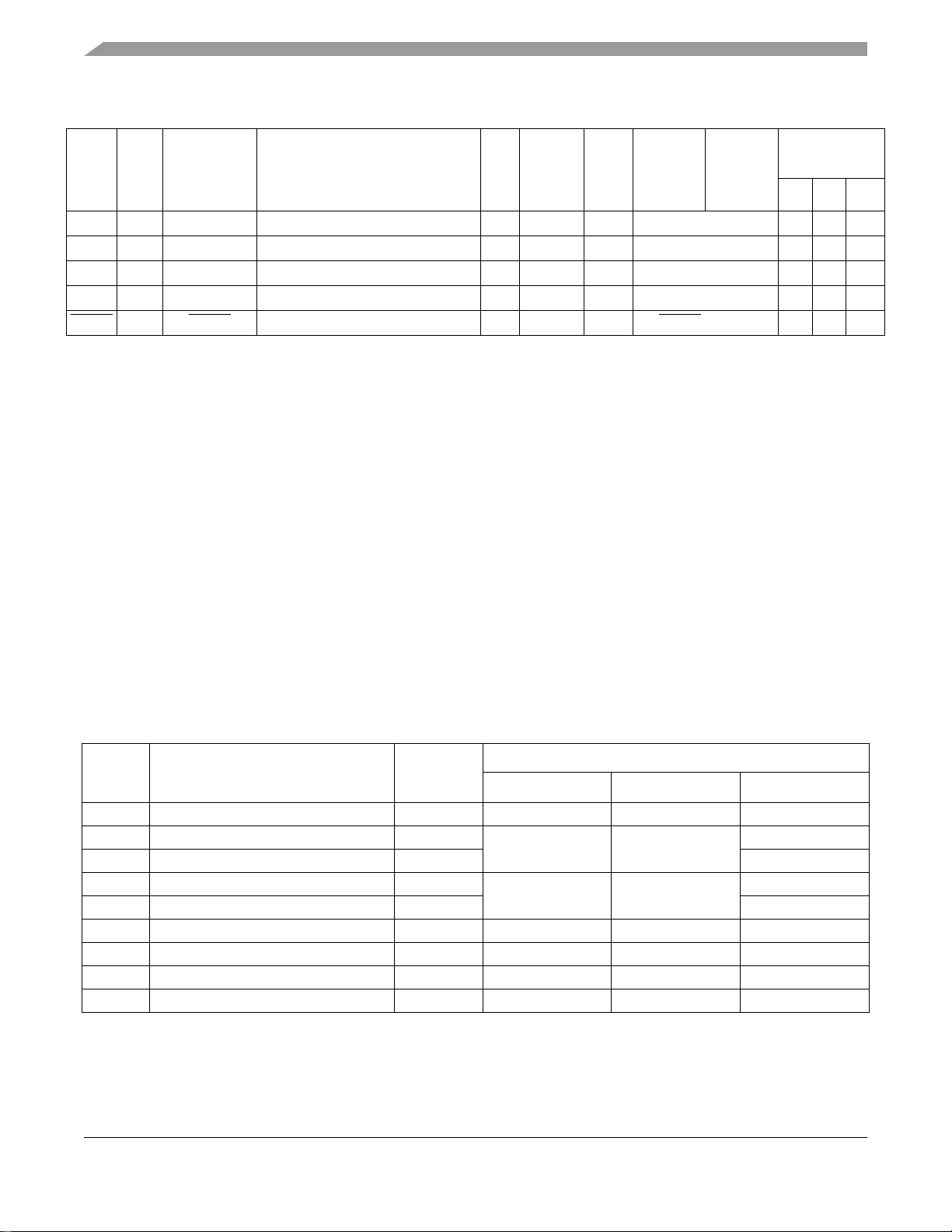
Signal Descriptions
Table 2-1. MPC5510 Signal Properties (continued)
GPIO
Pin
Name
JCOMP — JCOMP JTAG Compliancy I V
RESET
1
2
(PCR)
Num
TDO — TDO JTAG Test Data Output O V
TDI — TDI JTAG Test Data Input I V
TEST — TEST Test Mode Select I V
The GPIO number is the same as the corresponding pad configuration register (SIU_PCRn) number.
This column lists the functions associated with the programming of the SIU_PCRn[PA] bit field in the f ollowing order: GPIO, function
Supported
Functions
1
— RESET External Reset I/O V
2
Description
I/O
Type
Voltage
DDE3
DDE3
DDE3
DDE3
DDE2
Pad
3
Type
MH TDO (Pull Up9)7086T14
SH RESET (Pull Up) 10 10 E4
Status
During
Reset
IH TDI (Pull Up) 69 85 R13
IH JCOMP (Pull Down) 68 84 T13
IH TEST 62 78 R11
Status
After
4
Reset
Package Pin
Locations
4
144 176 208
1, function 2, and function 3. The unused functions by a given pin begin with function 3, then function 2, then function 1 (see
Figure 2-1).
3
These are nominal voltages. Each segment provides the power and ground for the given set of I/O pins.
4
A dash for the function in this column denotes the input and output buffer are turned off.
5
Port A[14:15]—EXT AL32 and XTAL32 functions only apply on the 144LQFP. These functions are on PortK[0:1] for the 176LQFP and
208BGA.
6
This analog input pin has reduced analog-to-digital conversion accuracy compared to P A0–PA15. See the MPC5510 Microcontroller
Family Data Sheet for values.
7
BOOTCFG is the pin function while the RESET pin is asserted. When the RESET pin is negated, the pin function is controlled by
the associated PCR register.
8
The NEXUS function is selected when the JTAG TAP controller is enabled via the JCOMP pin. The value of the PA field in the
associated PCR register has no effect on the pin function when the NEXUS function is selected.
9
Pullup is enabled only when JCOMP is negated.
2.3 Power and Ground Supply Summary
Refer to Section 2.7.12, “Power and Ground Pins,” for detailed descriptions of these pins.
Pin
Name
V
DDR
V
DDA
2
V
RH
V
SSA
3
V
RL
REFBYPC eQADC Reference Bypass Capacitor
4
V
PP
V
DDSYN
V
SSSYN
Function Description Voltage
Voltage Regulator Supply 5.0 V 46 56 T6
Analog Power
eQADC Voltage Reference High
Analog Ground
eQADC Voltage Reference Low –
Flash Program/Erase Power 5.0 V 78 94 P15
Clock Synthesizer Power 3.3 V 73 89 R16
Clock Synthesizer Ground – 76 92 M16
Table 2-2. MP C5 51 0 Power/Ground
1
144 176 208
5.0 V
5.0 V B3
–
V
SSA
144
141
1 1 B1
Package Pin Locations
176
173
A2
A4
B4
MPC5510 Microcontroller Family Reference Manual, Rev. 1
2-12 Freescale Semiconductor
Preliminary
Page 48
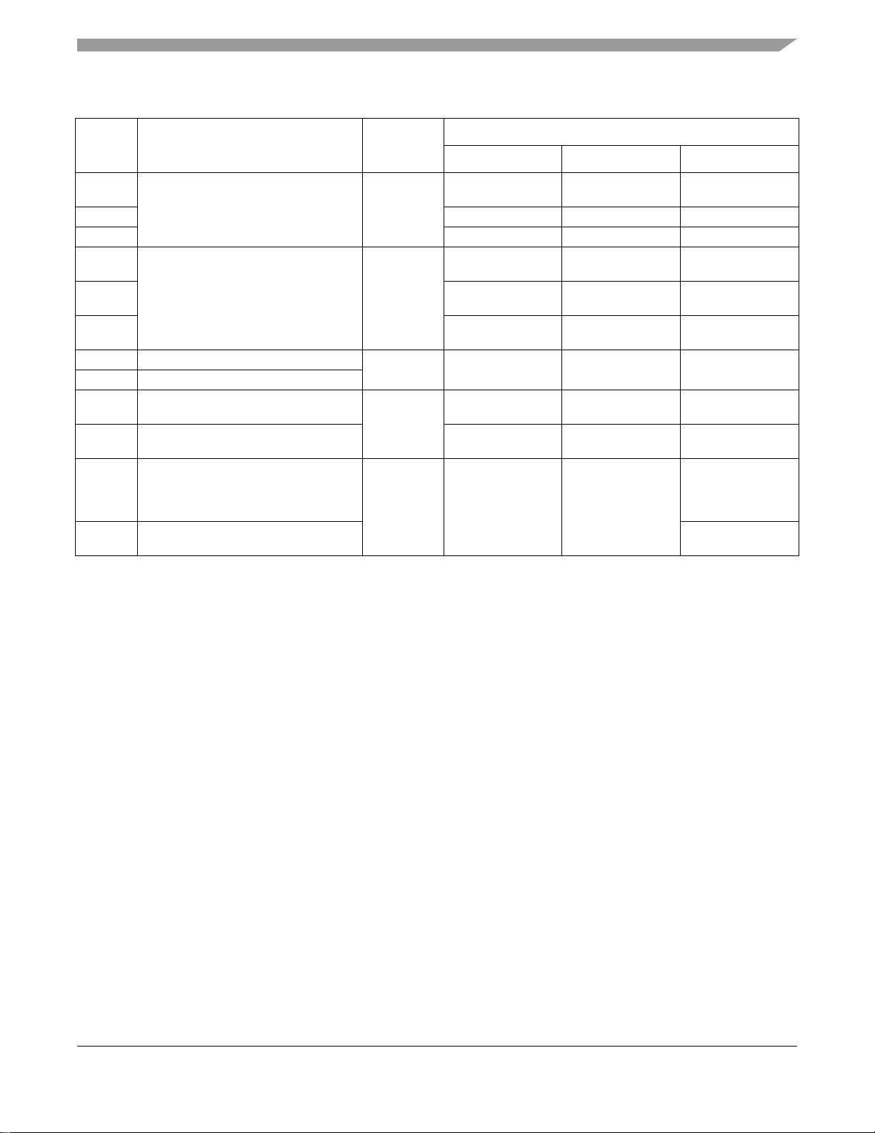
Table 2-2. MPC5510 Power/Ground (continued)
Signal Descriptions
Pin
Name
V
DDE1
V
DDE2
V
DDE3
V
SSE1
V
SSE2
V
SSE3
V
DD33
V
F:ASH
V
DD
Function Description Voltage
External I/O Power 3.3V – 5.0 V
External I/O Ground –
3.3 V I/O Power
5
Flash Read Power
Internal Logic Power
3.3 V
1
144 176 208
96,119
16,33,48 21,41,58 H4,L4,N5,P1
61 71,77 N9,T11
95,118
32,47 20,40,57
60 70,76
77 93 N15
31,53,79 39,63,95
1.5 V
V
DDF
V
SS
V
SSF
1
These are nominal voltages.
2
VRH is shorted to V
3
VRL is shorted to V
4
VPP requires nominal 5V for program/erase operations, but may be 0-5V otherwise.
5
V
is shorted to V
FLASH
Flash Internal Logic Power 79 95
Ground
–
80 96
Flash Internal Logic Ground
in the 144LQFP and 176LQFP packages.
DDA
in the 144LQFP and 176LQFP packages.
SSA
in the package.
DD33
Package Pin Locations
105,120,
143,155
104,119,
142,154
A15,D10,E13,
G16,K15
Shorted to V
package
Shorted to V
package
Shorted to V
package
SS
SS
SS
in the
in the
in the
A1,A16,B2,B15,
R2,R15,T1,T16
Shorted to VDD in the
package
C3,C14,D4,D13,
G7-G10,H7-H10,
J7-J10,K7-K10,
N4,N13,P3,P14
Shorted to V
package
SS
in the
MPC5510 Microcontroller Family Reference Manual, Rev. 1
Freescale Semiconductor 2-13
Preliminary
Page 49
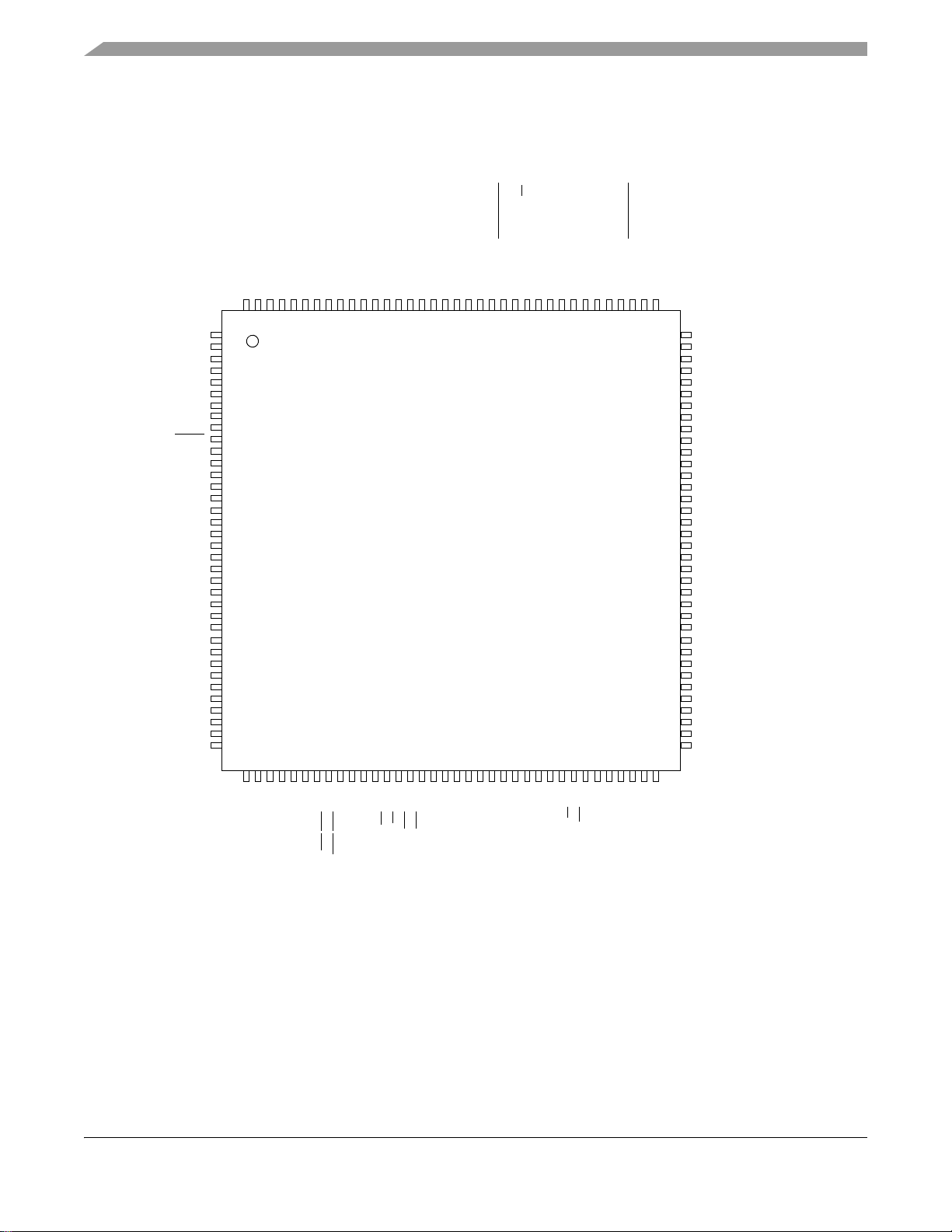
Signal Descriptions
PE0/PCS_A2/eMIOS5/MLBCLK
1
2
3
4
5
6
7
8
9
10
11
12
13
14
15
16
17
18
19
20
21
22
23
24
25
REFBYPC
AN7/PA7
AN6/PA6
AN5/PA5
AN4/PA4
AN3/PA3
AN1/PA1
AN0/PA0
RESET
CNTX_F/AN16/PH11
CNRX_F/AN17/PH10
CNRX_E/AN18/PH9
MA0/CNTX_E/AN19/PH8
V
SSE2
V
DDE2
RXD_F/AN20/PH7
TXD_F/AN21/PH6
MA1/RXD_E/AN22/PH5
MA2/TXD_E/AN23/PH4
CS[2]/eMIOS23/AN24/PH3
CS[3]/eMIOS22/AN25/PH2
SDA_A/eMIOS21/AN26/PH1
108
107
106
105
104
103
102
101
100
99
98
97
96
95
94
93
92
91
90
89
88
87
86
85
84
PC12/eMIOS12/PCS_C3/SIN_D
PC13/eMIOS13/PCS_A5/PCS_D[0]
PC14/eMIOS14/PCS_A4/PCS_D[1]
PC15/eMIOS15/PCS_A3/PCS_D[2]
PD0/CNTX_A/PCS_D[3]
PD1/CNRX_A/PCS_D[4]
PD2/CNRX_B/eMIOS10/PCS_D[5]/BOOTCFG*
PD3/CNTX_B/eMIOS11
PD4/CNTX_C/eMIOS12
PD5/CNRX_C/eMIOS13
PD6/TXD_A/eMIOS14
PD7/RXD_A/eMIOS15
V
DDE1
V
SSE1
PD8/TXD_B/SCL_A
PD9/RXD_B/SDA_A
PD10/PCS_B2/CNTX_F/NMI0
PD11/PCS_B1/CNRX_F/NMI1
PD12/PCS_B0/eMIOS9
PD13/SCK_B/eMIOS8
PD14/SOUT_B/eMIOS7
PE1/PCS_A1/eMIOS4/MLBSI
PE2/PCS_A0/eMIOS3/MLBDI
144
143
142
141
140
139
138
137
136
135
134
133
132
131
130
129
128
127
126
125
124
123
122
121
120
V
DDA
/V
RH
PA8/AN8
PA9/AN9
V
SSA
/V
RL
PA10/AN10
PA11/AN11
PA12/AN12
PA13/AN13
PA14/AN14/EXTAL32
PA15/AN15/XTAL32
PB0/AN28/eMIOS16/PCS_C5
PB1/AN29/eMIOS17/PCS_C4
PB2/AN30/eMIOS18/PCS_C3
PB3/AN31/PCS_C2
PB4/AN32/PCS_C1
PB5/AN33/PCS_C0
PB6/AN34/SCK_C
PB7/AN35/SOUT_C
PB8/AN36/SIN_C
PB9/AN37/CNTX_D/PCS_B4
PB10/AN38/CNRX_D/PCS_B3
PB11/AN39/eMIOS19/PCS_B5
PC0/eMIOS0/FR_A_TX_EN
/AD24
PC1/eMIOS1/FR_A_TX/AD16
PC2/eMIOS2/FR_A_RX/TS
37383940414243444546474849505152535455565758596061
eMIOS22/AD22/PG6
eMIOS21/AD21/PG5
PCS_C0/eMIOS20/AD20/PG4
SCK_C/eMIOS19/AD19/PG3
SOUT_C/eMIOS18/AD18/PG2
SIN_C/eMIOS17/AD17/PG1
eMIOS16/AD16/PG0
CNRX_D/TEA
/WE1/PF15
CNTX_D/BDIP
/WE0/PF14
V
DDR
V
SSE2
V
DDE2
RXD_D/OE/PF13
ALE/TXD_D/TS
/PF12
MDO7/RXD_C/CS0
/PF11
MDO6/TXD_C/CS1
/PF10
MDO5/ADDR15/AD15/PF9
MDO4/ADDR14/AD14/PF8
MDO3/ADDR13/AD13/PF7
MDO2/MLB_SLOT/ADDR12/AD12/PF6
MDO1/MLBDO/ADDR11/AD11/PF5
MDO0/MLBSO/ADDR10/AD10/PF4
V
SSE3
V
DDE3
SCL_A/eMIOS20/AN27/PH0
AN2/PA2
PD15/SIN_B/eMIOS6
26
27
28
29
30
31
32
33
34
35
36
SIN_A/AD31/PG15
SOUT_A/AD30/PG14
SCK_A/AD29/PG13
PCS_A0/AD28/PG12
PCS_A1/AD27/PG11
PCS_A2/AD26/PG10
V
SSE2
V
DDE2
TXD_C/PCS_A3/AD25/PG9
PCS_A4/AD24/PG8
RXD_C/eMIOS23/AD23/PG7
83
82
81
80
79
78
77
76
75
74
73
PE3/SCK_A/eMIOS2//MLBSO
PE4/SOUT_A/eMIOS1/MLBDO
PE5/SIN_A/eMIOS0/MLB_SLOT
V
SS/VSSF
VDD/V
DDF
V
PP
V
DD33/VFLASH
V
SSSYN
EXTAL
XTAL
V
DDSYN
6263646566676869707172
MCKO/MLBDI/ADDR9/AD9/PF3
MSEO/MLBSI /ADDR8/AD8/PF2
EVTO/MLBCLK/TA
/PF1
EVTI/RD_WR
/PF0
CLKOUT/PE6
JCOMP
TDI
TDO
TCK
TMS
119
118
117
116
115
114
113
112
111
110
109
V
DDE1VSSE1
PC3/eMIOS3/FR_DBG0
PC4/eMIOS4/FR_DBG1
PC5/eMIOS5/FR_DBG2
PC6/eMIOS6/FR_DBG3
PC7/eMIOS7/FR_B_RX
PC8/eMIOS8/FR_B_TX/AD15
PC9/eMIOS9/FR_B_TX_EN
/AD14
PC10/eMIOS10/PCS_C5/SCK_D
PC11/eMIOS11/PCS_C4/SOUT_D
Denotes active during RESET only*
V
DD
V
DD
TEST
144 LQFP
2.4 Pinout – 144 LQFP
Figure 2-2. MPC5510 Pinout – 144 LQFP
Preliminary
MPC5510 Microcontroller Family Reference Manual, Rev. 1
2-14 Freescale Semiconductor
Page 50
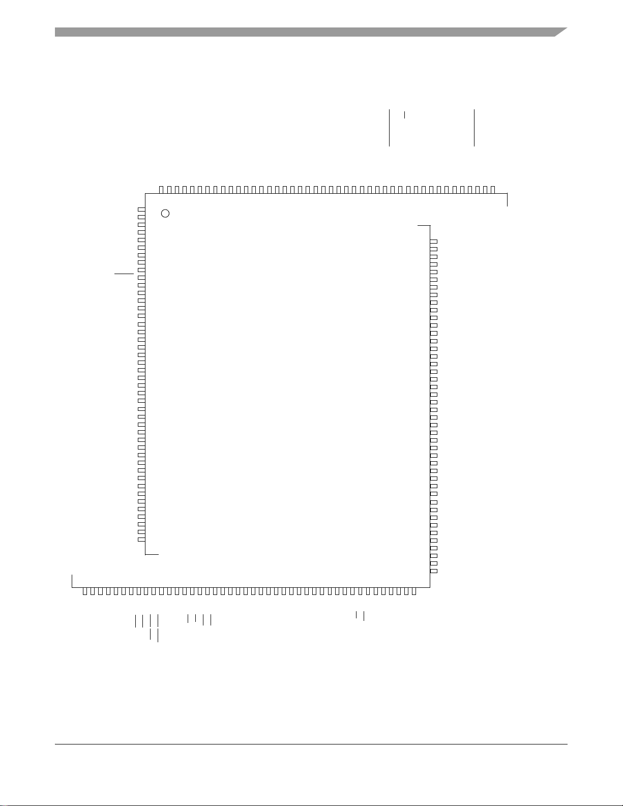
2.5 Pinout – 176 LQFP
PE0/PCS_A2/eMIOS5/MLBCLK
1
2
3
4
5
6
7
8
9
10
11
12
13
14
15
16
17
18
19
20
21
22
23
24
25
REFBYPC
AN7/PA7
AN6/PA6
AN5/PA5
AN4/PA4
AN3/PA3
AN1/PA1
AN0/PA0
RESET
CNTX_F/AN16/PH11
CNRX_F/AN17/PH10
CNRX_E/AN18/PH9
MA0/CNTX_E/AN19/PH8
V
SSE2
V
DDE2
RXD_F/AN20/PH7
TXD_F/AN21/PH6
MA1/RXD_E/AN22/PH5
MA2/TXD_E/AN23/PH4
CS[2]/eMIOS23/AN24/PH3
CS[3]/eMIOS22/AN25/PH2
SDA_A/eMIOS21/AN26/PH1
124
123
122
121
120
119
118
117
116
115
114
113
112
111
110
109
108
107
106
105
PC12/eMIOS12/PCS_C3/SIN_D
PC13/eMIOS13/PCS_A5/PCS_D[0]
PC14/eMIOS14/PCS_A4/PCS_D[1]
PC15/eMIOS15/PCS_A3/PCS_D[2]
PD0/CNTX_A/PCS_D[3]
PD1/CNRX_A/PCS_D[4]
PD2/CNRX_B/eMIOS10/PCS_D[5]/BOOTCFG*
PD3/CNTX_B/eMIOS11
PD4/CNTX_C/eMIOS12
PD5/CNRX_C/eMIOS13
PD6/TXD_A/eMIOS14
PD7/RXD_A/eMIOS15
V
DDE1
V
SSE1
PD8/TXD_B/SCL_A
PD9/RXD_B/SDA_A
PD10/PCS_B2/CNTX_F/NMI0
PD11/PCS_B1/CNRX_F/NMI1
PD12/PCS_B0/eMIOS9
PD13/SCK_B/eMIOS8
PD14/SOUT_B/eMIOS7
PE1/PCS_A1/eMIOS4/MLBSI
PE2/PCS_A0/eMIOS3/MLBDI
176
175
174
173
172
171
170
169
168
167
166
165
164
163
162
161
160
159
158
157
156
155
154
153
152
V
DDA
/V
RH
PA8/AN8
PA9/AN9
V
SSA
/V
RL
PA10/AN10
PA11/AN11
PA12/AN12
PA13/AN13
PA14/AN14
PA15/AN15
PB0/AN28/eMIOS16/PCS_C5
PB1/AN29/eMIOS17/PCS_C4
PB2/AN30/eMIOS18/PCS_C3
PB3/AN31/PCS_C2
PB4/AN32/PCS_C1
PB5/AN33/PCS_C0
PB6/AN34/SCK_C
PB7/AN35/SOUT_C
PB8/AN36/SIN_C
PB9/AN37/CNTX_D/PCS_B4
PB10/AN38/CNRX_D/PCS_B3
PB11/AN39/eMIOS19/PCS_B5
PC0/eMIOS0/FR_A_TX_EN
/AD24
PC1/eMIOS1/FR_A_TX/AD16
PC2/eMIOS2/FR_A_RX/TS
53545556575859606162636465666768697071727374757677
CNTX_D/BDIP
/WE0/PF14
V
DDR
V
SSE2
V
DDE2
RXD_D/OE/PF13
ALE/TXD_D/TS
/PF12
MDO7/RXD_C/CS0
/PF11
MDO6/TXD_C/CS1
/PF10
MDO5/ADDR15/AD15/PF9
MDO4/ADDR14/AD14/PF8
MDO3/ADDR13/AD13/PF7
MDO1/MLBDO/ADDR11/AD11/PF5
MDO0/MLBSO/ADDR10/AD10/PF4
V
SSE3
V
DDE3
SCL_A/eMIOS20/AN27/PH0
AN2/PA2
PD15/SIN_B/eMIOS6
26
27
28
29
30
31
32
33
34
35
36
SIN_A/AD31/PG15
SOUT_A/AD30/PG14
SCK_A/AD29/PG13
PCS_A0/AD28/PG12
PCS_A1/AD27/PG11
PCS_A2/AD26/PG10
V
SSE2
V
DDE2
TXD_C/PCS_A3/AD25/PG9
PCS_A4/AD24/PG8
RXD_C/eMIOS23/AD23/PG7
PE3/SCK_A/eMIOS2//MLBSO
PE4/SOUT_A/eMIOS1/MLBDO
PE5/SIN_A/eMIOS0/MLB_SLOT
V
SS/VSSF
VDD/V
DDF
V
PP
V
DD33/VFLASH
V
SSSYN
EXTAL
XTAL
V
DDSYN
7879808182838485868788
MCKO/MLBDI/ADDR9/AD9/PF3
MSEO/MLBSI/ADDR8/AD8/PF2
EVTO/MLBCLK/TA
/PF1
EVTI/RD_WR
/PF0
CLKOUT/PE6
JCOMP
TDI
TDO
TCK
TMS
151
150
149
148
147
146
145
144
143
142
141
V
DDE1VSSE1
PC3/eMIOS3/FR_DBG0
PC4/eMIOS4/FR_DBG1
PC5/eMIOS5/FR_DBG2
PC6/eMIOS6/FR_DBG3
PC7/eMIOS7/FR_B_RX
PC8/eMIOS8/FR_B_TX/AD15
PC9/eMIOS9/FR_B_TX_EN
/AD14
PC10/eMIOS10/PCS_C5/SCK_D
PC11/eMIOS11/PCS_C4/SOUT_D
Denotes active during RESET only*
V
DD
V
DD
VSUP/TEST
176 LQFP
37
38
39
40
41
42
43
44
140
139
138
137
136
135
134
133
45464748495051
52
eMIOS22/AD22/PG6
eMIOS21/AD21/PG5
PCS_C0/eMIOS20/AD20/PG4
SCK_C/eMIOS19/AD19/PG3
SOUT_C/eMIOS18/AD18/PG2
SIN_C/eMIOS17/AD17/PG1
eMIOS16/AD16/PG0
CNRX_D/TEA
/WE1/PF15
104
103
102
101
100
99
98
97
96
95
94
93
92
91
90
89
132
131
130
129
128
127
126
125
SIN_D/PJ15
SOUT_D/PJ14
SCK_D/PJ13
PCS_D0/PJ12
PCS_D1/PJ11
PCS_D2/PJ10
PCS_D3/PJ9
PCS_D4/PJ8
WE3/PH15
WE2
/PH14
AD7/PJ7
AD6/PJ6
AD5/PJ5
AD4/PJ4
V
DDE3
V
SSE3
PE10
PE11
PE12
PE13
V
DDE1
V
SSE1
PE14
PE15
PB15/RXD_H
PB14/TXD_H
V
DDE1VSSE1
PK0/EXTAL32
PK1/XTAL32
PB12/TXD_G/PCS_B4
PB13/RXD_G/PCS_B3
Signal Descriptions
Freescale Semiconductor 2-15
Figure 2-3. MPC5510 Pinout – 176 LQFP
MPC5510 Microcontroller Family Reference Manual, Rev. 1
Preliminary
Page 51
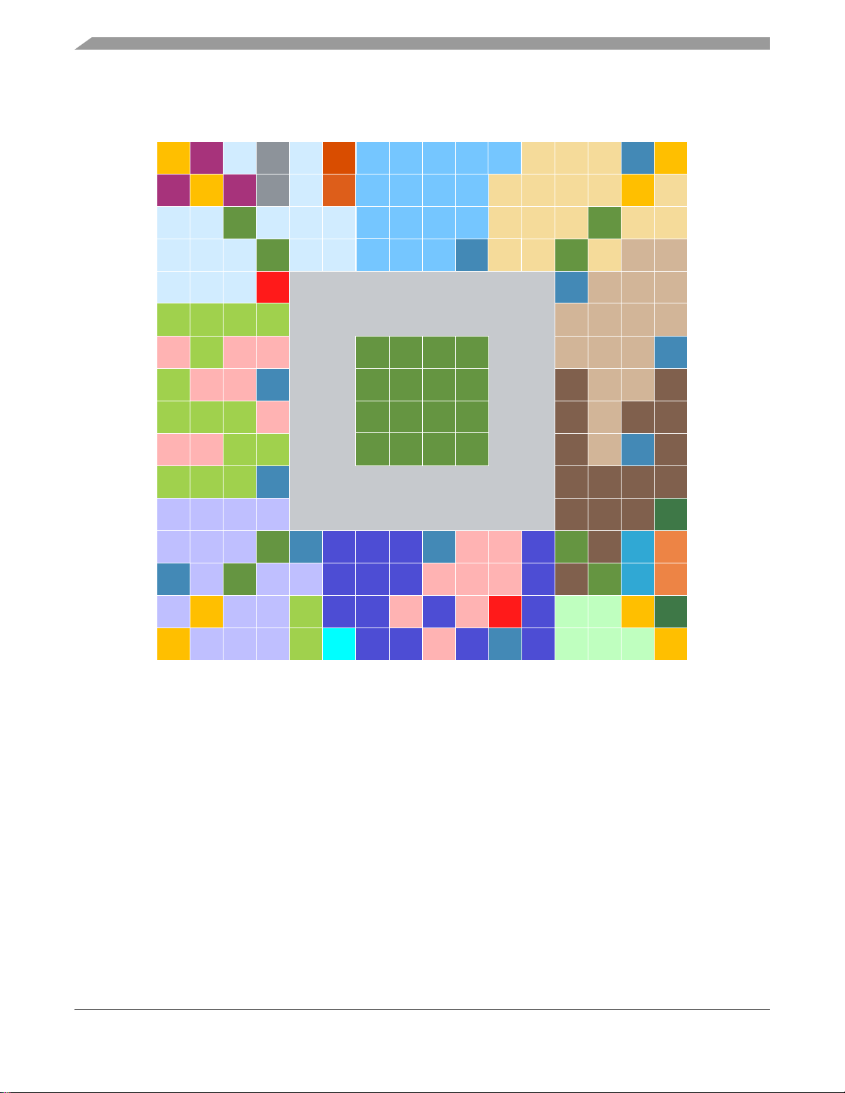
Signal Descriptions
V
DD
12345678910111213141516
V
DDA
PA8 V
SSA
PB2 PB6 PC3 PC7 PC10 V
DDE1VDD
A
REF
VDDVRHVRLPA12 PK0
PB3 PB7 PC0 PC4 PC8 PC11 V
DD
PC12
B
VSSPA9 PA11 PA15
PB4 PB8 PB14 PC1 PC5 PC9 VSSPC13 PC14
C
VSSPA10 PA14
PB5 V
DDE1
VSSPC15 PD0 PD1
D
V
DDE1
PD2 PD3 PD4
E
PD6 PD7 PD9
F
PD8
G
V
SS
VSSVSSV
SS
V
SS
VSSVSSV
SS
V
SS
VSSVSSV
SS
PE8
H
V
SS
VSSVSSV
SS
PE9 PD14 PE11 PE10
J
PE12 PD15 V
DDE1
PE0
K
PE13 PE1 PE14
L
PE3
M
VSSV
DDE2
PF0 V
SS
N
VSSPG3
PF1
PF3
VSSVPPXTAL
P
VDDPG5
PF2 TDI TCK V
DD
R
VDDPG6
PE6
JCOMP V
DD
T
A
B
C
D
E
F
G
H
J
K
L
M
12345678910111213141516
PA13
208 PBGA Ball Map
(as viewed from top through the package)
N
P
R
T
PB10
PB11
PD10 PD11 V
DDE1
PF15
PG4
PA6
PA3
RESET
PK1
PA7
PA5
PB9
PD13PD12PE7
PA4
PA0
PH10
PG7
EXTAL
PF14
TMS
PC6
PD5
PE2
PE15 PE5
V
SSSYN
PE4 V
DD33
PJ0PJ2V
DDE3
PF8PF12
PA1PA2
PH11PH12PH13
PJ13PJ14PH9PJ15
V
DDE2
PJ11PJ12PH8
PJ10PH5PH6PH7
PH3PH4PJ8PJ9
V
DDE2
PH0PH1PH2
PG12PG13PG14PG15
PG9PG10PG11
PG8V
DDE2
PG0 PJ1PJ4PF7PF11 PJ6
PG2 PF13PH15 TESTPJ3PJ7PF10 PF5
PG1 V
DDR
PH14 V
DDE3
PF4PF6PF9 PJ5
TDO
V
DDSYN
PB12
PB13
PB15
PB0
PC2
PB1
BYPC
2.6 Pinout – 208 BGA
2.7 Detailed External Signal Descriptions
Figure 2-4. MPC5510 Pinout – 208 PBGA
2.7.1 Port A Pins
2.7.1.1 PA0 to PA13 — GPI (PA[0:13]) / Analog Input (AN[0] – AN[13])
PA[0:13] are general-purpose input (GPI) pins. AN[0] to AN[13] are single-ended analog input pins.
2-16 Freescale Semiconductor
MPC5510 Microcontroller Family Reference Manual, Rev. 1
Preliminary
Page 52

Signal Descriptions
2.7.1.2 PA14 — GPI (PA[14]) / Analog Input (AN[14]) / 32 kHz Crystal Input
(EXTAL32)
PA[14] is a general-purpose input (GPI) pin. AN[14] is a single-ended analog input pin. EXTAL32 is the
input pin for an external 32 kHz crystal oscillator (EXTAL32 function available on PA[14] pin on the
144LQFP package and PK[0] pin on the 176LQFP and 208BGA packages).
2.7.1.3 PA15 — GPI (PA[15]) / Analog Input (AN[15]) / 32 kHz Crystal Output
(XTAL32)
PA[15] is a GPI pin. AN[15] is a single-ended analog input pin. XTAL32 is the output pin for an external
32 kHz crystal oscillator (XTAL32 function available on PA[15] pin on the 144LQFP package and PK[1]
pin on the 176LQFP and 208BGA packages).
2.7.2 Port B Pins
2.7.2.1 PB0 — GPIO (PB[0]) / Analog Input (AN[28]) / eMIOS Channel
(eMIOS[16]) / DSPI_C Peripheral Chip Select (PCS_C[5])
PB[0] is a GPIO pin. AN[28] is a single-ended analog input pin. eMIOS[16] is an output-only channel pin
for the eMIOS200 module. PCS_C[5] is a peripheral chip select output pin for the DSPI C module.
2.7.2.2 PB1 — GPIO (PB[1]) / Analog Input (AN[29]) / eMIOS Channel
(eMIOS[17]) / DSPI_C Peripheral Chip Select (PCS_C[4])
PB[1] is a GPIO pin. AN[29] is a single-ended analog input pin. eMIOS[17] is an output-only channel pin
for the eMIOS200 module. PCS_C[4] is a peripheral chip select output pin for the DSPI C module.
2.7.2.3 PB2 — GPIO (PB[2]) / Analog Input (AN[30]) / eMIOS Channel
(eMIOS[18]) / DSPI_C Peripheral Chip Select (PCS_C[3])
PB[2] is a GPIO pin. AN[30] is a single-ended analog input pin. eMIOS[18] is an output-only channel pin
for the eMIOS200 module. PCS_C[3] is a peripheral chip select output pin for the DSPI C module.
2.7.2.4 PB3 — GPIO (PB[3]) / Analog Input (AN[31]) / DSPI_C Peripheral Chip
Select (PCS_C[2])
PB[3] is a GPIO pin. AN[31] is a single-ended analog input pin. PCS_C[2] is a peripheral chip select
output pin for the DSPI C module.
2.7.2.5 PB4 — GPIO (PB[4]) / Analog Input (AN[32]) / DSPI_C Peripheral Chip
Select (PCS_C[1])
PB[4] is a GPIO pin. AN[32] is a single-ended analog input pin. PCS_C[1] is a peripheral chip select
output pin for the DSPI C module.
MPC5510 Microcontroller Family Reference Manual, Rev. 1
Freescale Semiconductor 2-17
Preliminary
Page 53

Signal Descriptions
2.7.2.6 PB5 — GPIO (PB[5]) / Analog Input (AN[33]) / DSPI_C Peripheral Chip
Select (PCS_C[0])
PB[5] is a GPIO pin. AN[33] is a single-ended analog input pin. PCS_C[0] is a peripheral chip select
output pin for the DSPI C module.
2.7.2.7 PB6 — GPIO (PB[6]) / Analog Input (AN[34]) / DSPI_C Clock (SCK_C)
PB[6] is a GPIO pin. AN[34] is a single-ended analog input pin. SCK_C is the SPI clock pin for the DSPI
C module.
2.7.2.8 PB7 — GPIO (PB[7]) / Analog Input (AN[35]) / DSPI_C Data Output
(SOUT_C)
PB[7] is a GPIO pin. AN[35] is a single-ended analog input pin. SOUT_C is the data output pin for the
DSPI C module.
2.7.2.9 PB8 — GPIO (PB[8]) / Analog Input (AN[36]) / DSPI_C Data Input (SIN _C)
PB[8] is a GPIO pin. AN[36] is a single-ended analog input pin. SIN_C is the data input pin for the DSPI
C module.
2.7.2.10 PB9 — GPIO (PB[9]) / Analog Input (AN[37]) / CAN_D T ransmit (CNTX_D)
/ DSPI_B Peripheral Chip Select (PCS_B[4])
PB[9] is a GPIO pin. AN[37] is a single-ended analog input pin. CNTX_D is the transmit pin for the
FlexCan D module. PCS_B[4] is a peripheral chip select output pin for the DSPI B module.
2.7.2.11 PB10 — GPIO (PB[10]) / Analog Input (AN[38]) / CAN_D Receive
(CNRX_D) / DSPI_B Peripheral Chip Select (PCS_B[3])
PB[10] is a GPIO pin. AN[38] is a single-ended analog input pin. CNRX_D is the receive pin for the
FlexCan D module. PCS_B[3] is a peripheral chip select output pin for the DSPI B module.
2.7.2.12 PB11 — GPIO (PB[11]) / Analog Input (AN[39]) / eMIOS Channel
(eMIOS[19]) / DSPI_B Peripheral Chip Select (PCS_B[5])
PB[11] is a GPIO pin. AN[39] is a single-ended analog input pin. eMIOS[19] is an output-only channel
pin for the eMIOS200 module. PCS_B[5] is a peripheral chip select output pin for the DSPI B module.
2.7.2.13 PB12 — GPIO (PB[12]) / SCI_G Transmit (TXD_G) / DSPI_B Peripheral
Chip Select (PCS_B[4])
PB[12] is a GPIO pin. TXD_G is the transmit pin for the eSCI G module. PCS_B[4] is a peripheral chip
select output pin for the DSPI B module.
MPC5510 Microcontroller Family Reference Manual, Rev. 1
2-18 Freescale Semiconductor
Preliminary
Page 54

Signal Descriptions
2.7.2.14 PB13 — GPIO (PB[13]) / SCI_G Receive (RXD_G) / DSPI_B Peripheral
Chip Select (PCS_B[3])
PB[13] is a GPIO pin. RXD_G is the receive pin for the eSCI G module. PCS_B[3] is a peripheral chip
select output pin for the DSPI B module.
2.7.2.15 PB14 — GPIO (PB[14]) / SCI_H Transmit (TXD_H)
PB[14] is a GPIO pin. TXD_H is the transmit pin for the eSCI H module.
2.7.2.16 PB15 — GPIO (PB[15]) / SCI_H Receive (RXD_H)
PB[15] is a GPIO pin. RXD_H is the receive pin for the eSCI H module.
2.7.3 Port C Pins
2.7.3.1 PC0 — GPIO (PC[0]) / eMIOS Channel (eMIOS[0]) / FlexRay Channel A
T ransmit Enable (FR_A_TX_EN
PC[0] is a GPIO pin. eMIOS[0] is an input/output channel pin for the eMIOS200 module. FR_A_TX_EN
in the FlexRay Channel A transmit enable pin. AD[24] is the external bus interface (EBI) multiplexed
address and data bus.
) / EBI Multiplexed Address/Data (AD[24])
2.7.3.2 PC1 — GPIO (PC[1]) / eMIOS Channel (eMIOS[1]) / FlexRay Channel A
Transmit (FR_A_TX) / EBI Multiplexed Address/Data (AD[16])
PC[1] is a GPIO pin. eMIOS[1] is an input/output channel pin for the eMIOS200 module. FR_A_TX in
the FlexRay Channel A transmit pin. AD[16] is the EBI multiplexed address and data bus
2.7.3.3 PC2 — GPIO (PC[2]) / eMIOS Channel (eMIOS[2]) / FlexRay Channel A
Receive (FR_A_RX) / EBI Transfer Start (TS
PC[2] is a GPIO pin. eMIOS[2] is an input/output channel pin for the eMIOS200 module. FR_A_RX in
the FlexRay Channel A receive pin. TS
is the EBI transfer start signal.
)
2.7.3.4 PC3 — GPIO (PC[3]) / eMIOS Channel (eMIOS[3]) / FlexRay Debug 0
(FR_DBG0)
PC[3] is a GPIO pin. eMIOS[3] is an input/output channel pin for the eMIOS200 module. FR_DBG0 is
one of the FlexRay debug port pins.
2.7.3.5 PC4 — GPIO (PC[4]) / eMIOS Channel (eMIOS[4]) / FlexRay Debug 1
(FR_DBG1)
PC[4] is a GPIO pin. eMIOS[4] is an input/output channel pin for the eMIOS200 module. FR_DBG1 is
one of the FlexRay debug port pins.
MPC5510 Microcontroller Family Reference Manual, Rev. 1
Freescale Semiconductor 2-19
Preliminary
Page 55

Signal Descriptions
2.7.3.6 PC5 — GPIO (PC[5]) / eMIOS Channel (eMIOS[5]) / FlexRay Debug 2
(FR_DBG2)
PC[5] is a GPIO pin. eMIOS[5] is an input/output channel pin for the eMIOS200 module. FR_DBG2 is
one of the FlexRay debug port pins.
2.7.3.7 PC6 — GPIO (PC[6]) / eMIOS Channel (eMIOS[6]) / FlexRay Debug 3
(FR_DBG3)
PC[3] is a GPIO pin. eMIOS[6] is an input/output channel pin for the eMIOS200 module. FR_DBG3 is
one of the FlexRay debug port pins.
2.7.3.8 PC7 — GPIO (PC[7]) / eMIOS Channel (eMIOS[7]) / FlexRay Channel B
Receive (FR_B_RX)
PC[7] is a GPIO pin. eMIOS[7] is an input/output channel pin for the eMIOS200 module. FR_B_RX is
the FlexRay Channel B receive pin.
2.7.3.9 PC8 — GPIO (PC[8]) / eMIOS Channel (eMIOS[8]) / FlexRay Channel B
Transmit (FR_B_TX) / Multiplexed Address/Data (AD[15])
PC[8] is a GPIO pin. eMIOS[8] is an input/output channel pin for the eMIOS200 module. FR_B_TX is
the FlexRay Channel B transmit pin. AD[15] is the EBI multiplexed address and data bus.
2.7.3.10 PC9 — GPIO (PC[9]) / eMIOS Channel (eMIOS[9]) / FlexRay Channel B
Transmit Enable (FR_B_TX_EN
PC[9] is a GPIO pin. eMIOS[9] is an input/output channel pin for the eMIOS200 module. FR_B_TX_EN
is the FlexRay Channel B transmit enable pin. AD[14] is the EBI multiplexed address and data bus.
) / Multiplexed Address/Data (AD[14])
2.7.3.11 PC10 — GPIO (PC[10]) / eMIOS Channel (eMIOS[10]) / DSPI_C Peripheral
Chip Select (PCS_C[5]) / DSPI_D Clock (SCK_D)
PC[10] is a GPIO pin. eMIOS[10] is an input/output channel pin for the eMIOS200 module. PCS_C[5] is
a peripheral chip select output pin for the DSPI C module. SCK_D is the SPI clock pin of the DSPI_D
module.
2.7.3.12 PC11 — GPIO (PC[11]) / eMIOS Channel (eMIOS[11]) / DSPI_C Peripheral
Chip Select (PCS_C[4]) / DSPI_D Serial Data Out (SOUT_D)
PC[11] is a GPIO pin. eMIOS[11] is an input/output channel pin for the eMIOS200 module. PCS_C[4] is
a peripheral chip select output pin for the DSPI C module. SOUT_D is the serial data output from the
DSPI_D module.
MPC5510 Microcontroller Family Reference Manual, Rev. 1
2-20 Freescale Semiconductor
Preliminary
Page 56

Signal Descriptions
2.7.3.13 PC12 — GPIO (PC[12]) / eMIOS Channel (eMIOS[12]) / DSPI_C Peripheral
Chip Select (PCS_C[3]) / DSPI_D Serial Data Input (SIN_D)
PC[12] is a GPIO pin. eMIOS[12] is an input/output channel pin for the eMIOS200 module. PCS_C[3] is
a peripheral chip select output pin for the DSPI C module. SIN_D is the serial data input for the DSPI_D
module.
2.7.3.14 PC13 — GPIO (PC[13]) / eMIOS Channel (eMIOS[13]) / DSPI_A Peripheral
Chip Select (PCS_A[5]) / DSPI_D Peripheral Chip Select (PCS_D[0])
PC[13] is a GPIO pin. eMIOS[13] is an input/output channel pin for the eMIOS200 module. PCS_A[5] is
a peripheral chip select output pin for the DSPI A module. PCS_D[0] is a peripheral chip select output pin
for the DSPI_D module.
2.7.3.15 PC14 — GPIO (PC[14]) / eMIOS Channel (eMIOS[14]) / DSPI_A Peripheral
Chip Select (PCS_A[4]) / DSPI_D Peripheral Chip Select (PCS_D[1])
PC[14] is a GPIO pin. eMIOS[14] is an input/output channel pin for the eMIOS200 module. PCS_A[4] is
a peripheral chip select output pin for the DSPI A module. PCS_D[1] is a peripheral chip select output pin
for the DSPI D module.
2.7.3.16 PC15 — GPIO (PC[15]) / eMIOS Channel (eMIOS[15]) / DSPI_A Peripheral
Chip Select (PCS_A[3]) / DSPI_D Peripheral Chip Select (PCS_D[2])
PC[15] is a GPIO pin. eMIOS[15] is an input/output channel pin for the eMIOS200 module. PCS_A[3] is
a peripheral chip select output pin for the DSPI A module. PCS_D[2] is a peripheral chip select output pin
for the DSPI D module.
2.7.4 Port D Pins
2.7.4.1 PD0 — GPIO (PD[0]) / CAN_A Transmit (CNTX_A) / DSPI_D Peripheral
Chip Select (PCS_D[3])
PD[0] is a GPIO pin. CNTX_A is the transmit pin for the FlexCan A module. PCS_D[3] is a peripheral
chip select for the DSPI_D module.
2.7.4.2 PD1 — GPIO (PD[1]) / CAN_A Receive (CNRX_A) / DSPI_D Peripheral
Chip Select (PCS_D[4])
PD[1] is a GPIO pin. CNRX_A is the receive pin for the FlexCan A module. PCS_D[4] is a peripheral
chip select for the DSPI_D module.
MPC5510 Microcontroller Family Reference Manual, Rev. 1
Freescale Semiconductor 2-21
Preliminary
Page 57

Signal Descriptions
2.7.4.3 PD2 — GPIO (PD[2]) / CAN_B Receive (CNRX_B) / eMIOS Channel
(eMIOS[10]) / Boot Configuration (BOOTCFG) / DSPI_D Peripheral Chip
Select (PCS_D[5])
PD[2] is a GPIO pin. CNRX_B is the receive pin for the FlexCan B module. eMIOS[10] is an output-only
channel pin for the eMIOS200 module. The BOOTCFG pin is sampled before the negation of the RESET
pin. The value is used by the BAM program to determine the boot configuration. PCS_D[5] is a peripheral
chip select output pin for the DSPI_D module.
2.7.4.4 PD3 — GPIO (PD[3]) / CAN_B Transmit (CNTX_B) / eMIOS Channel
(eMIOS[11])
PD[3] is a GPIO pin. CNTX_B is the transmit pin for the FlexCan B module. eMIOS[11] is an output-only
channel pin for the eMIOS200 module.
2.7.4.5 PD4 — GPIO (PD[4]) / CAN_C Transmit (CNTX_C) / eMIOS Channel
(eMIOS[12])
PD[4] is a GPIO pin. CNTX_C is the transmit pin for the FlexCan C module. eMIOS[12] is an output-only
channel pin for the eMIOS200 module.
2.7.4.6 PD5 — GPIO (PD[5]) / CAN_C Receive (CNRX_C) / eMIOS Channel
(eMIOS[13])
PD[5] is a GPIO pin. CNRX_C is the receive pin for the FlexCan C module. eMIOS[13] is an output-only
channel pin for the eMIOS200 module.
2.7.4.7 PD6 — GPIO (PD[6]) / SCI_A Transmit (TXD_A) / eMIOS Channel
(eMIOS[14])
PD[6] is a GPIO pin. TXD_A is the transmit pin for the eSCI_A module. eMIOS[14] is an output-only
channel pin for the eMIOS200 module.
2.7.4.8 PD7 — GPIO (PD[7]) / SCI_A Receive (RXD_A) / eMIOS Channel
(eMIOS[15])
PD[7] is a GPIO pin. RXD_A is the receive pin for the eSCI_A module. eMIOS[15] is an output-only
channel pin for the eMIOS200 module.
2.7.4.9 PD8 — GPIO (PD[8]) / SCI_B Transmit (TXD_B) / I2C Serial Clock Line
(SCL_A)
PD[8] is a GPIO pin. TXD_B is the transmit pin for the eSCI_B module. SCL_A is the serial clock signal
for the I2C_A module.
MPC5510 Microcontroller Family Reference Manual, Rev. 1
2-22 Freescale Semiconductor
Preliminary
Page 58

Signal Descriptions
2.7.4.10 PD9 — GPIO (PD[9]) / SCI_B Receive (RXD_B) / I2C Serial Data Line
(SDA_A)
PD[9] is a GPIO pin. RXD_B is the receive pin for the eSCI_B module. SDA_A is the serial data line for
the I2C_A module.
2.7.4.11 PD10 — GPIO (PD[10]) / DSPI_B Peripheral Chip Select (PCS_B[2]) /
CAN_F Transmit (CNTX_F) / e200z1 Critical Interrupt (NMI0)
PD[10] is a GPIO pin. PCS_B[2] is a peripheral chip select output pin for the DSPI B module. CNTX_F
is the transmit pin for the FlexCan F module. NMI0 is the critical interrupt input for the e200z1 core.
2.7.4.12 PD11 — GPIO (PD[11]) / DSPI_B Peripheral Chip Select (PCS_B[1]) /
CAN_F Receive (CNRX_F) / e200z0 Critical Interrupt (NMI1)
PD[11] is a GPIO pin. PCS_B[1] is a peripheral chip select output pin for the DSPI B module. CNRX_F
is the receive pin for the FlexCan F module. NMI1 is the critical interrupt input for the e200z0 core.
2.7.4.13 PD12 — GPIO (PD[12]) / DSPI_B Peripheral Chip Select (PCS_B[0]) /
eMIOS Channel (eMIOS[9])
PD[12] is a GPIO pin. PCS_B[0] is a peripheral chip select output pin for the DSPI B module. eMIOS[9]
is an output-only channel pin for the eMIOS200 module.
2.7.4.14 PD13 — GPIO (PD[13]) / DSPI_B Clock (SCK_B) / eMIOS Channel
(eMIOS[8])
PD[13] is a GPIO pin. SCK_B is the SPI clock pin for the DSPI B module. eMIOS[8] is an output-only
channel pin for the eMIOS200 module.
2.7.4.15 PD14 — GPIO (PD[14]) / DSPI_B Data Output (SOUT_B) / eMIOS Channel
(eMIOS[7])
PD[14] is a GPIO pin. SOUT_B is the data output pin for the DSPI B module. eMIOS[7] is an output-only
channel pin for the eMIOS200 module.
2.7.4.16 PD15 — GPIO (PD[15]) / DSPI_B Data Input (SIN_B) / eMIOS Channel
(eMIOS[6])
PD[15] is a GPIO pin. SIN_B is the data input pin for the DSPI B module. eMIOS[6] is an output-only
channel pin for the eMIOS200 module.
MPC5510 Microcontroller Family Reference Manual, Rev. 1
Freescale Semiconductor 2-23
Preliminary
Page 59

Signal Descriptions
2.7.5 Port E Pins
2.7.5.1 PE0 — GPIO (PE[0]) / DSPI_A Peripheral Chip Select (PCS_A[2]) / eMIOS
Channel (eMIOS[5]) / MLB Clock (MLBCLK)
PE[0] is a GPIO pin. PCS_A[2] is a peripheral chip select output pin for the DSPI A module. eMIOS[5]
is an output-only channel pin for the eMIOS200 module. MLBCLK is the clock pin for the emulated MLB
module.
2.7.5.2 PE1 — GPIO (PE[1]) / DSPI_A Peripheral Chip Select (PCS_A[1]) / eMIOS
Channel (eMIOS[4]) / MLB Signal In / Signal (MLBSI / MLBSIG)
PE[1] is a GPIO pin. PCS_A[1] is a peripheral chip select output pin for the DSPI A module. eMIOS[4]
is an output-only channel pin for the eMIOS200 module. In a 3-pin MLB interface, MLBSIG is the
bidirectional signal line that transfers bus management data to/from the MOST network controller. In a
5-pin interface, MLBSI carries signal line data from the MOST network controller to the emulated MLB
module.
2.7.5.3 PE2 — GPIO (PE[2]) / DSPI_A Peripheral Chip Select (PCS_A[0]) / eMIOS
Channel (eMIOS[3]) / MLB Data In / Data (MLBDI / MLBDAT)
PE[2] is a GPIO pin. PCS_A[0] is a peripheral chip select output pin for the DSPI A module. eMIOS[3]
is an output-only channel pin for the eMIOS200 module. In a 3-pin MLB interface, MLBDAT is the
bidirectional data line that transfers user data to/from the MOST network controller. In a 5-pin MLB
interface, MLBDI carries user data from the MOST network controller to the emulated MLB module.
2.7.5.4 PE3 — GPIO (PE[3]) / DSPI_A Clock (SCK_A) / eMIOS Channel
(eMIOS[2]) / MLB Signal Out / Level Shifter Enable (MLBSO /
MLBSIG_BUFEN)
PE[3] is a GPIO pin. SCK_A is the SPI clock pin for the DSPI A module. eMIOS[2] is an output-only
channel pin for the eMIOS200 module. In a 3-pin MLB interface, MLBSIG_BUFEN controls the external
level shifter for the MLBSIG pin. In a 5-pin MLB interface, MLBSO carries signal data from the emulated
MLB module to the MOST network controller.
2.7.5.5 PE4 — GPIO (PE[4]) / DSPI_A Data Output (SOUT_A) / eMIOS Channel
(eMIOS[1]) / MLB Data Out / Level Shifter Enable (MLBDO /
MLBDAT_BUFEN)
PE[4] is a GPIO pin. SOUT_A is the data output pin for the DSPI A module. eMIOS[1] is an output-only
channel pin for the eMIOS200 module. In a 3-pin MLB interface, MLBDA T_BUFEN controls the external
level shifter for the MLBDAT pin. In a 5-pin MLB interface, MLBDO carries user data from the emulated
MLB module to the MOST network controller.
MPC5510 Microcontroller Family Reference Manual, Rev. 1
2-24 Freescale Semiconductor
Preliminary
Page 60

Signal Descriptions
2.7.5.6 PE5 — GPIO (PE[5]) / DSPI_A Data Input (SIN_A) / eMIOS Channel
(eMIOS[0]) / MLB SLOT / Signal Observe / Data Observe (MLB_SLOT /
MLB_SIGOBS / MLB_DATOBS)
PE[5] is a GPIO pin. SIN_A is the data input pin for the DSPI A module. eMIOS[0] is an output-only
channel pin for the eMIOS200 module. MLB_SLOT, MLB_SIGOBS, and MLB_DATOBS are debug
signals for the MLB module.
2.7.5.7 PE6 — GPIO (PE[6]) / Clock Output (CLKOUT)
PE[6] is a GPIO pin. CLKOUT is the external bus interface clock output.
2.7.5.8 PE7 to PE15 — GPIO (PE[7:15])
PE[7:15] are GPIO pins.
2.7.6 Port F Pins
2.7.6.1 PF0 — GPIO (PF[0]) / EBI Read/Write (RD_WR) / Nexus Event In (EVTI)
PF[0] is a GPIO pin. RD_WR indicates whether an external bus transfer is a read or write operation. EVTI
is an input that is read on the assertion of JCOMP to enable or disable the Nexus Debug port. After reset,
the EVTI pin initiates program and data trace synchronization messages or generates a breakpoint.
2.7.6.2 PF1 — GPIO (PF[1]) / EBI T ransf er Ac kno wledge (TA) / Nexus Event Out
(EVTO
PF[1] is a GPIO pin. TA indicates to the external bus master that the slave has completed the current
transfer . EVTO is an output providing timing to a development tool for a single watch point or breakpoint
occurrence. MLBCLK is the clock pin for the emulated MLB module.
) / MLB Clock (MLBCLK)
2.7.6.3 PF2 — GPIO (PF[2]) / EBI Multiplex Address/Data (AD[8]) / EBI Non
Muxed Address (ADDR[8]) / MLB Signal In / Signal (MLBSI / MLBSIG) /
Nexus Message Start/End Out (MSEO
PF[2] is a GPIO pin. AD[8] is the EBI multiplexed address and data bus. ADDR[8] is the EBI non
multiplexed address bus. In a 3-pin MLB interface, MLBSIG is the bidirectional signal line that transfers
bus management data to/from the MOST network controller. In a 5-pin interface, MLBSI carries signal
line data from the MOST network controller to the emulated MLB module. MSEO is an output that
indicates when messages start and end on the MDO pins.
)
MPC5510 Microcontroller Family Reference Manual, Rev. 1
Freescale Semiconductor 2-25
Preliminary
Page 61

Signal Descriptions
2.7.6.4 PF3 — GPIO (PF[3]) / EBI Multiplex Address/Data (AD[9]) / EBI Non
Muxed Address (ADDR[9]) / MLB Data In / Data (MLBDI / MLBDAT) /
Nexus Message Clock Out (MCKO)
PF[3] is a GPIO pin. AD[9] is the EBI multiplexed address and data bus. ADDR[9] is the EBI non
multiplexed address bus. In a 3-pin MLB interface, MLBDAT is the bidirectional data line that transfers
user data to/from the MOST network controller. In a 5-pin MLB inte rface, MLBDI carries user data from
the MOST network controller to the emulated MLB module. MCKO is a free running clock output to the
development tools that is used for timing of the MDO and MSEO signals.
2.7.6.5 PF4 — GPIO (PF[4]) / EBI Multiplex Address/Data (AD[10]) / EBI Non
Muxed Address (ADDR[10]) / MLB Signal Out / Level Shifter Enable
(MLBSO / MLBSIG_BUFEN) / Nexus Message Data Out (MDO[0])
PF[4] is a GPIO pin. AD[10] is the EBI multiplexed address and data bus. ADDR[10] is the EBI non
multiplexed address bus. In a 3-pin MLB interface, MLBSIG_BUFEN controls the external level shifter
for the MLBSIG pin. In a 5-pin MLB interface, MLBSO carries signal data from the emulated MLB
module to the MOST network controller. MDO[0] is a trace message output to the development tools.
2.7.6.6 PF5 — GPIO (PF[5]) / EBI Multiplex Address/Data (AD[11]) / EBI Non
Muxed Address (ADDR[11]) / MLB Data Out / Level Shifter Enable
(MLBDO / MLBDAT_BUFEN) / Nexus Message Data Out (MDO[1])
PF[5] is a GPIO pin. AD[11] is the EBI multiplexed address and data bus. ADDR[11] is the EBI non
multiplexed address bus. In a 3-pin MLB interface, MLBDAT_BUFEN controls the external level shifter
for the MLBDAT pin. In a 5-pin MLB interface, MLBDO carries user data from the emulated MLB
module to the MOST network controller. MDO[1] is a trace message output to the development tools.
2.7.6.7 PF6 — GPIO (PF[6]) / EBI Multiplex Address/Data (AD[12]) / EBI Non
Muxed Address (ADDR[12]) / MLB SLO T / Signal Observe / Data Observe
(MLB_SLOT / MLB_SIGOBS / MLB_DATOBS) / Nexus Message Data Out
(MDO[2])
PF[6] is a GPIO pin. AD[12] is the EBI multiplexed address and data bus. ADDR[12] is the EBI non
multiplexed address bus. MLB_SLOT, MLB_SIGOBS, and MLB_DATOBS are debug signals for the
MLB module. MDO[2] is a trace message output to the development tools.
2.7.6.8 PF7 — GPIO (PF[7]) / EBI Multiplex Address/Data (AD[13]) / EBI Non
Muxed Address (ADDR[13]) / Nexus Message Data Out (MDO[3])
PF[7] is a GPIO pin. AD[13] is the EBI multiplexed address and data bus. ADDR[13] is the EBI non
multiplexed address bus. MDO[3] is a trace message output to the development tools.
MPC5510 Microcontroller Family Reference Manual, Rev. 1
2-26 Freescale Semiconductor
Preliminary
Page 62

Signal Descriptions
2.7.6.9 PF8 — GPIO (PF[8]) / EBI Multiplex Address/Data (AD[14]) / EBI Non
Muxed Address (ADDR[14]) / Nexus Message Data Out (MDO[4])
PF[8] is a GPIO pin. AD[14] is the EBI multiplexed address and data bus. ADDR[14] is the EBI non
multiplexed address bus. MDO[4] is a trace message output to the development tools.
2.7.6.10 PF9 — GPIO (PF[9]) / EBI Multiplex Address/Data (AD[15]) / EBI Non
Muxed Address (ADDR[15]) / Nexus Message Data Out (MDO[5])
PF[9] is a GPIO pin. AD[15] is the EBI multiplexed address and data bus. ADDR[15] is the EBI non
multiplexed address bus. MDO[5] is a trace message output to the development tools.
2.7.6.11 PF10 — GPIO (PF[10]) / EBI Chip Select (CS[1]) / SCI_C T ransmit (TXD_C)
/ Nexus Message Data Out (MDO[6])
PF[10] is a GPIO pin. CS[1] is the EBI chip select output signals. TXD_C is the transmit pin for the eSCI
C module. MDO[6] is a trace message output to the development tools.
2.7.6.12 PF11 — GPIO (PF[11]) / EBI Chip Select (CS[0]) / SCI_C Receive (RXD_C)
/ Nexus Message Data Out (MDO[7])
PF[11] is a GPIO pin. CS[0] is the EBI chip select output signals . RXD_C is the receive pin for the eSCI
C module. MDO[7] is a trace message output to the development tools.
2.7.6.13 PF12 — GPIO (PF[12]) / EBI T ransfer Start (TS) / SCI_D T ransmit (TXD_D)
/ EBI Address Latch Enable
PF[12] is a GPIO pin. TS is the EBI transfer start output signals. TXD_D is the transmit pin for the eSCI
D module. ALE is the EBI address latch enable.
2.7.6.14 PF13 — GPIO (PF[13]) / EBI Output Enable (OE) / SCI_D Receive (RXD_D)
PF[13] is a GPIO pin. OE is the EBI chip select output signals. RXD_D is the receive pin for the eSCI D
module.
2.7.6.15 PF14 — GPIO (PF[14]) / EBI Write Enable (WE[0]) / EBI Burst Data In
Progress (BDIP
PF[14] is a GPIO pin. WE[0] specifies which data pins contain valid data for an external bus transfer . BDIP
indicates that an EBI burst transfer is in progress. CNTX_D is the transmit pin for the FlexCan D module.
) / CAN_D Transmit (CNTX_D)
2.7.6.16 PF15 — GPIO (PF[15]) / EBI Write Enable (WE[1]) / EBI Transfer Error
Acknowledge (TEA
) / CAN_D Receive (CNRX_D)
PF[15] is a GPIO pin. WE[1] specifies which data pins contain valid data for an external bus transfer. TEA
indicates that an error occurred in the current external bus transfer. CNRX_D is the receive pin for the
FlexCan D module.
MPC5510 Microcontroller Family Reference Manual, Rev. 1
Freescale Semiconductor 2-27
Preliminary
Page 63

Signal Descriptions
2.7.7 Port G Pins
2.7.7.1 PG0 — GPIO (PG[0]) / EBI Multiplex Address/Data (AD[16]) / eMIOS
Channel (eMIOS[16])
PG[0] is a GPIO pin. AD[16] is the EBI multiplexed address and data bus. eMIOS[16] is an input/output
channel pin for the eMIOS200 module.
2.7.7.2 PG1 — GPIO (PG[1]) / EBI Multiplex Address/Data (AD[17]) / eMIOS
Channel (eMIOS[17]) / DSPI_C Data In (SIN_C)
PG[1] is a GPIO pin. AD[17] is the EBI multiplexed address and data bus. eMIOS[17] is an input/output
channel pin for the eMIOS200 module. SIN_C is the data input pin for the DSPI C module.
2.7.7.3 PG2 — GPIO (PG[2]) / EBI Multiplex Address/Data (AD[18]) / eMIOS
Channel (eMIOS[18]) / DSPI_C Data Out (SOUT_C)
PG[2] is a GPIO pin. AD[18] is the EBI multiplexed address and data bus. eMIOS[18] is an input/output
channel pin for the eMIOS200 module. SOUT_C is the data output pin for the DSPI C module.
2.7.7.4 PG3 — GPIO (PG[3]) / EBI Multiplex Address/Data (AD[19]) / eMIOS
Channel (eMIOS[19]) / DSPI_C Serial Clock (SCK_C)
PG[3] is a GPIO pin. AD[19] is the EBI multiplexed address and data bus. eMIOS[19] is an input/output
channel pin for the eMIOS200 module. SCK_C is the SPI clock pin for the DSPI C module.
2.7.7.5 PG4 — GPIO (PG[4]) / EBI Multiplex Address/Data (AD[20]) / eMIOS
Channel (eMIOS[20]) / DSPI_C Peripheral Chip Select (PCS_C[0])
PG[4] is a GPIO pin. AD[20] is the EBI multiplexed address and data bus. eMIOS[20] is an input/output
channel pin for the eMIOS200 module. PCS_C[0] is a peripheral chip select output pin for the DSPI C
module.
2.7.7.6 PG5 — GPIO (PG[5]) / EBI Multiplex Address/Data (AD[21]) / eMIOS
Channel (eMIOS[21])
PG[5] is a GPIO pin. AD[21] is the EBI multiplexed address and data bus. eMIOS[21] is an input/output
channel pin for the eMIOS200 module.
2.7.7.7 PG6 — GPIO (PG[6]) / EBI Multiplex Address/Data (AD[22]) / eMIOS
Channel (eMIOS[22])
PG[6] is a GPIO pin. AD[22] is the EBI multiplexed address and data bus. eMIOS[22] is an input/output
channel pin for the eMIOS200 module.
MPC5510 Microcontroller Family Reference Manual, Rev. 1
2-28 Freescale Semiconductor
Preliminary
Page 64

Signal Descriptions
2.7.7.8 PG7 — GPIO (PG[7]) / EBI Multiplex Address/Data (AD[23]) / eMIOS
Channel (eMIOS[23]) / SCI_C Receive (RXD_C)
PG[7] is a GPIO pin. AD[23] is the EBI multiplexed address and data bus. eMIOS[23] is an input/output
channel pin for the eMIOS200 module. RXD_C is the receive pin for the eSCI C module.
2.7.7.9 PG8 — GPIO (PG[8]) / EBI Multiplex Address/Data (AD[24]) / DSPI_A
Peripheral Chip Select (PCS_A[4])
PG[8] is a GPIO pin. AD[24] is the EBI multiplexed address and data bus. PCS_A[4] is a peripheral chip
select output pin for the DSPI A module.
2.7.7.10 PG9 — GPIO (PG[9]) / EBI Multiplex Address/Data (AD[25]) / DSPI_A
Peripheral Chip Select (PCS_A[3]) / SCI_C Transmit (TXD_C)
PG[9] is a GPIO pin. AD[25] is the EBI multiplexed address and data bus. PCS_A[3] is a peripheral chip
select output pin for the DSPI A module. TXD_C is the transmit pin for the eSCI_C module.
2.7.7.11 PG10 — GPIO (PG[10]) / EBI Multiplex Address/Data (AD[26]) / DSPI_A
Peripheral Chip Select (PCS_A[2])
PG[10] is a GPIO pin. AD[26] is the EBI multiplexed address and data bus. PCS_A[2] is a peripheral chip
select output pin for the DSPI A module.
2.7.7.12 PG11 — GPIO (PG[11]) / EBI Multiplex Address/Data (AD[27]) / DSPI_A
Peripheral Chip Select (PCS_A[1])
PG[11] is a GPIO pin. AD[27] is the EBI multiplexed address and data bus. PCS_A[1] is a peripheral chip
select output pin for the DSPI A module.
2.7.7.13 PG12 — GPIO (PG[12]) / EBI Multiplex Address/Data (AD[28]) / DSPI_A
Peripheral Chip Select (PCS_A[0])
PG[12] is a GPIO pin. AD[28] is the EBI multiplexed address and data bus. PCS_A[0] is a peripheral chip
select output pin for the DSPI A module.
2.7.7.14 PG13 — GPIO (PG[13]) / EBI Multiplex Address/Data (AD[29]) / DSPI_A
Serial Clock (SCK_A)
PG[13] is a GPIO pin. AD[29] is the EBI multiplexed address and data bus. SCK_A is the SPI clock pin
for the DSPI A module.
2.7.7.15 PG14 — GPIO (PG[14]) / EBI Multiplex Address/Data (AD[30]) / DSPI_C
Data Out (SOUT_A)
PG[14] is a GPIO pin. AD[24] is the EBI multiplexed address and data bus. SOUT_A is the data output
pin for the DSPI A module.
MPC5510 Microcontroller Family Reference Manual, Rev. 1
Freescale Semiconductor 2-29
Preliminary
Page 65

Signal Descriptions
2.7.7.16 PG15 — GPIO (PG[15]) / EBI Multiplex Address/Data (AD[31]) / DSPI_C
Data In (SIN_A)
PG[15] is a GPIO pin. AD[31] is the EBI multiplexed address and data bus. SIN_A is the data input pin
for the DSPI A module.
2.7.8 Port H Pins
2.7.8.1 PH0 — GPIO (PH[0]) / Analog Input (AN[27]) / eMIOS Channel
(eMIOS[20]) / I
PH[0] is a GPIO pin. AN[27] is a single-ended analog input pin. eMIOS[20] is an output-only channel pin
for the eMIOS200 module. SCL_A is the serial clock signal for the I2C_A module.
2
C Serial Clock Line (SCL_A)
2.7.8.2 PH1 — GPIO (PH[1]) / Analog Input (AN[26]) / eMIOS Channel
(eMIOS[21]) / I
PH[1] is a GPIO pin. AN[26] is a single-ended analog input pin. eMIOS[21] is an output-only channel pin
for the eMIOS200 module. SDA_A is the serial data signal for the I2C_A module.
2
C Serial Data Line (SDA_A)
2.7.8.3 PH2 — GPIO (PH[2]) / Analog Input (AN[25]) / eMIOS Channel
(eMIOS[22]) / EBI Chip Select (CS[3]
PH[2] is a GPIO pin. AN[25] is a single-ended analog input pin. eMIOS[22] is an output-only channel pin
for the eMIOS200 module. CS[3] is an EBI chip select output.
)
2.7.8.4 PH3 — GPIO (PH[3]) / Analog Input (AN[24]) / eMIOS Channel
(eMIOS[23]) / EBI Chip Select (CS[2]
PH[3] is a GPIO pin. AN[24] is a single-ended analog input pin. eMIOS[23] is an output-only channel pin
for the eMIOS200 module. CS[2] is an EBI chip select output.
)
2.7.8.5 PH4 — GPIO (PH[4]) / Analog Input (AN[23]) / SCI_E Transmit (TXD_E) /
External Analog Mux Address Output (MA[2])
PH[4] is a GPIO pin. AN[23] is a single-ended analog input pin. TXD_E is the transmit pin for the eSCI_E
module. MA[2] is a address output for an external analog mux used to select the mux input channel to
connect to the QADC.
2.7.8.6 PH5 — GPIO (PH[5]) / Analog Input (AN[22]) / SCI_E Receive (RXD_E) /
External Analog Mux Address Output (MA[1])
PH[5] is a GPIO pin. AN[22] is a single-ended analog input pin. RXD_E is the receive pin for the eSCI_E
module. MA[1] is a address output for an external analog mux used to select the mux input channel to
connect to the QADC.
MPC5510 Microcontroller Family Reference Manual, Rev. 1
2-30 Freescale Semiconductor
Preliminary
Page 66

Signal Descriptions
2.7.8.7 PH6 — GPIO (PH[6]) / Analog Input (AN[21]) / SCI_E Transmit (TXD_F)
PH[6] is a GPIO pin. AN[21] is a single-ended analog input pin. TXD_F is the transmit pin for the eSCI_F
module.
2.7.8.8 PH7 — GPIO (PH[7]) / Analog Input (AN[20]) / SCI_F Receive (RXD_F)
PH[7] is a GPIO pin. AN[20] is a single-ended analog input pin. RXD_F is the receive pin for the eSCI_F
module.
2.7.8.9 PH8 — GPIO (PH[8]) / Analog Input (AN[19]) / CAN_E T ransmit (CNTX_E)
/ External Analog Mux Address Output (MA[0])
PH[8] is a GPIO pin. AN[19] is a single-ended analog input pin. CNTX_E is the transmit pin for the
FlexCAN_E module. MA[0] is a address output for an external analog mux used to select the mux input
channel to connect to the QADC.
2.7.8.10 PH9 — GPIO (PH[9]) / Analog Input (AN[18]) / CAN_E Receive (CNRX_E)
PH[9] is a GPIO pin. AN[18] is a single-ended analog input pin. CNRX_E is the receive pin for the
FlexCAN_E module.
2.7.8.11 PH10 — GPIO (PH[10]) / Analog Input (AN[17]) / CAN_F Receive
(CNRX_F)
PH[10] is a GPIO pin. AN[17] is a single-ended analog input pin. CNRX_F is the receive pin for the
FlexCAN_F module.
2.7.8.12 PH11 — GPIO (PH[11]) / Analog Input (AN[16]) / CAN_F Transmit
(CNTX_F)
PH[11] is a GPIO pin. AN[16] is a single-ended analog input pin. CNTX_F is the transmit pin for the
FlexCAN_F module.
2.7.8.13 PH12 — GPIO (PH[12]) / DSPI_D Peripheral Chip Select (PCS_D[5])
PH[12] is a GPIO pin. PCS_D[5] is a peripheral chip select output pin for the DSPI_D module.
2.7.8.14 PH13 — GPIO (PH[13])
PH[13] is a GPIO pin.
2.7.8.15 PH14 — GPIO (PH[14]) / EBI Write Enable (WE[2])
PH[14] is a GPIO pin. WE[2] specifies which data pins contain valid data for an external bus transfer.
MPC5510 Microcontroller Family Reference Manual, Rev. 1
Freescale Semiconductor 2-31
Preliminary
Page 67

Signal Descriptions
2.7.8.16 PH15 — GPIO (PH[15]) / EBI Write Enable (WE[3])
PH[15] is a GPIO pin. WE[3] specifies which data pins contain valid data for an external bus transfer.
2.7.9 Port J Pins
2.7.9.1 PJ0 to PJ7 — GPIO (PJ[0:7]) / EBI Multiplex Address/Data (AD[0:7])
PJ[0:7] are GPIO pins. AD[0:7] are EBI multiplexed address and data bus pins.
2.7.9.2 PJ8 — GPIO (PJ8) / DSPI_D Peripheral Chip Select (PCS_D[4])
PJ8 is a GPIO pin. PCS_D[4] is a peripheral chip select output pin for the DSPI_D module.
2.7.9.3 PJ9 — GPIO (PJ9) / DSPI_D Peripheral Chip Select (PCS_D[3])
PJ9 is a GPIO pin. PCS_D[3] is a peripheral chip select output pin for the DSPI_D module.
2.7.9.4 PJ10 — GPIO (PJ10) / DSPI_D Peripheral Chip Select (PCS_D[2])
PJ10 is a GPIO pin. PCS_D[2] is a peripheral chip select output pin for the DSPI_D module.
2.7.9.5 PJ11 — GPIO (PJ11) / DSPI_D Peripheral Chip Select (PCS_D[1])
PJ11 is a GPIO pin. PCS_D[1] is a peripheral chip select output pin for the DSPI_D module.
2.7.9.6 PJ12 — GPIO (PJ12) / DSPI_D Peripheral Chip Select (PCS_D[0])
PJ12 is a GPIO pin. PCS_D[0] is a peripheral chip select output pin for the DSPI_D module.
2.7.9.7 PJ13 - GPIO (PJ13) / DSPI_D Clock (SCK_D)
PJ13 is a GPIO pin. SCK_D is the SPI clock pin of the DSPI_D module.
2.7.9.8 PJ14 - GPIO (PJ14) / DSPI_D Serial Data Out (SOUT_D)
PJ14 is a GPIO pin. SOUT_D is the SPI serial data out for the DSPI_D module.
2.7.9.9 PJ15 - GPIO (PJ15) / DSPI_D Serial Data In (SIN_D)
PJ15 is a GPIO pin. SIN_D is the SPI serial data in for the DSPI_D module.
MPC5510 Microcontroller Family Reference Manual, Rev. 1
2-32 Freescale Semiconductor
Preliminary
Page 68

Signal Descriptions
2.7.10 Port K Pins
2.7.10.1 PK0 — GPI (PK0) / 32 kHz Crystal Input (EXTAL32)
PK0 is a GPI pin. EXTAL32 is the input pin for an external 32 kHz crystal oscillator. (The EXTAL32
function is available on the PA14 pin on the 144LQFP package and on the PK0 pin on the 176LQFP and
208BGA packages.)
2.7.10.2 PK1 — GPI (PK[1]) / 32 kHz Crystal Output (XTAL32)
PK1 is a GPI pin. XTAL32 is the output pin for an external 32 kHz crystal oscillator (XTAL32 function
available on A15 pin on the 144LQFP package and PK1 pin on the 176LQFP and 208BGA packages).
2.7.11 Miscellaneous Pins
2.7.11.1 XTAL — Crystal Oscillator Output
XTAL is the output pin for an external crystal oscillator.
2.7.11.2 EXTAL — Crystal Oscillat or Input / External Clock Input
EXT AL is the input pin for an external crystal oscillator or an external clock source. The alternate function
is the external clock input.
2.7.11.3 RESET — External Reset Input
The RESET pin is a bidirectional I/O pin. It is asserted by an external device to reset all modules of the
MCU, except the R TC counter. It is also an open drain output signal that is asserted during an internal reset.
See Chapter 7, “Reset,” for more detail.
2.7.11.4 TCK — JTAG Test Clock Input
TCK provides the clock input for the on-chip test logic.
2.7.11.5 TDI — JTAG Test Data Input
TDI provides the serial test instruction and data input for the on-chip test logic.
2.7.11.6 TDO — JTAG Test Data Output
TDO provides the serial test data output for the on-chip test logic.
2.7.11.7 TMS — JTAG Test Mode Select Input
TMS controls test mode operations for the on-chip test logic.
MPC5510 Microcontroller Family Reference Manual, Rev. 1
Freescale Semiconductor 2-33
Preliminary
Page 69

Signal Descriptions
2.7.11.8 JCOMP — JTAG Compliance Input
The JCOMP pin is used to enable the JTAG TAP controller.
2.7.11.9 TEST — Test Mode Enable Input
The TEST pin is used to place the chip in test mode. It must be negated for normal operation, and should
be connected to ground in all customer applications.
2.7.12 Power and Ground Pins
2.7.12.1 Voltage Regulator Reference (VDDR)
VDDR is the voltage reference to the internal voltage regulator.
2.7.12.2 VDDA — Analog-to-Digital Converter Analog Supply
VDDA is the analog supply for the eQADC.
2.7.12.3 VSSA — Analog-to-Digital Converter Analog Ground
VSSA is the analog ground for the eQADC.
2.7.12.4 VRH — Analog-to-Digital Converter Reference High
VRH is the reference high input for the eQADC.
2.7.12.5 VRL — Analog-to-Digital Converter Reference Low
VRL is the reference low input for the eQADC.
2.7.12.6 REFBYPC — Reference Bypass Capacitor
REFBYPC is a bypass capacitor input for the eQADC. The REFBYPC pin is used to connect an external
bias capacitor between the REFBYPC pin and VRL.
2.7.12.7 VDDSYN — Clock Synthesizer Supply
VDDSYN is the supply power for the FMPLL.
2.7.12.8 VSSSYN — Clock Synthesizer Ground
VSSSYN is the ground reference for the FMPLL.
MPC5510 Microcontroller Family Reference Manual, Rev. 1
2-34 Freescale Semiconductor
Preliminary
Page 70

Signal Descriptions
2.7.12.9 VDD33 — 3.3 V I/O and Flash Read Supply (VFLASH)
VDD33 is the 3.3 V internal supply used for the external I/O control logic. It is intended only for the
connection of bypass capacitors, and must not be connect to load or power . (VFLASH is the on-chip flash
read supply.)
2.7.12.10 VPP — Flash Program/Erase Supply
VPP is the on-chip flash program/erase supply.
2.7.12.11 VDD — Internal Logic Supply and Flash Logic Supply (VDDF)
VDD is the 1.5 V logic and flash supply.
2.7.12.12 VSS — Internal Logic and Flash (VSSF) Ground
VSS is the ground reference for internal logic and the flash.
2.7.12.13 VDDEx — External I/O Supply
VDDEx is the 3.3 V to 5.0 V external I/O supply independently controlling the level for one of three
groups of I/O pins. (x=1,2,3.)
2.7.12.14 VSSEx — External I/O Ground
VSSEx is the external I/O ground for one of three groups of I/O pins. (x=1,2,3.)
MPC5510 Microcontroller Family Reference Manual, Rev. 1
Freescale Semiconductor 2-35
Preliminary
Page 71

Signal Descriptions
MPC5510 Microcontroller Family Reference Manual, Rev. 1
2-36 Freescale Semiconductor
Preliminary
Page 72

Chapter 3
System Clock Description
3.1 Introduction
The MPC5510 supports several clock sources that include an internal phase-locked loop (PLL), an
external high-frequency crystal (XOSC), an external low-frequency crystal (32kOSC), an internal
high-frequency RC oscillator (IRC), and an internal low-frequency RC oscillator (32kRC).
The availability of the clock sources vary, depending on the run, stop, and power mode selected. During
low power modes, the PLL and XOSC are not available as clock sources.
The internal system clock may be generated in several ways:
• Internal 16 MHz IRC
• PLL: Normal mode with crystal clock reference for XOSC
• PLL: Normal mode with external clock reference for XOSC
• XOSC with external clock reference (PLL bypass mode)
• XOSC with crystal clock reference
There are two clock output pins driven by programmable clock dividers: CLKOUT and MCKO.
The oscillator clock can be selected as the clock source for the FlexCAN interface in the FlexCAN blocks
resulting in very low jitter performance. The oscillator clock can also be selected as the clock source for
the FlexRay interface in the FlexRay block.
The default clock source after reset is the 16 MHz IRC.
3.2 Clock Sources
The various clock sources that are available on MPC5510 are shown in Figure 3-1 and discussed in more
detail in subsequent sections.
MPC5510 Microcontroller Family Reference Manual, Rev. 1
Freescale Semiconductor 3-1
Preliminary
Page 73
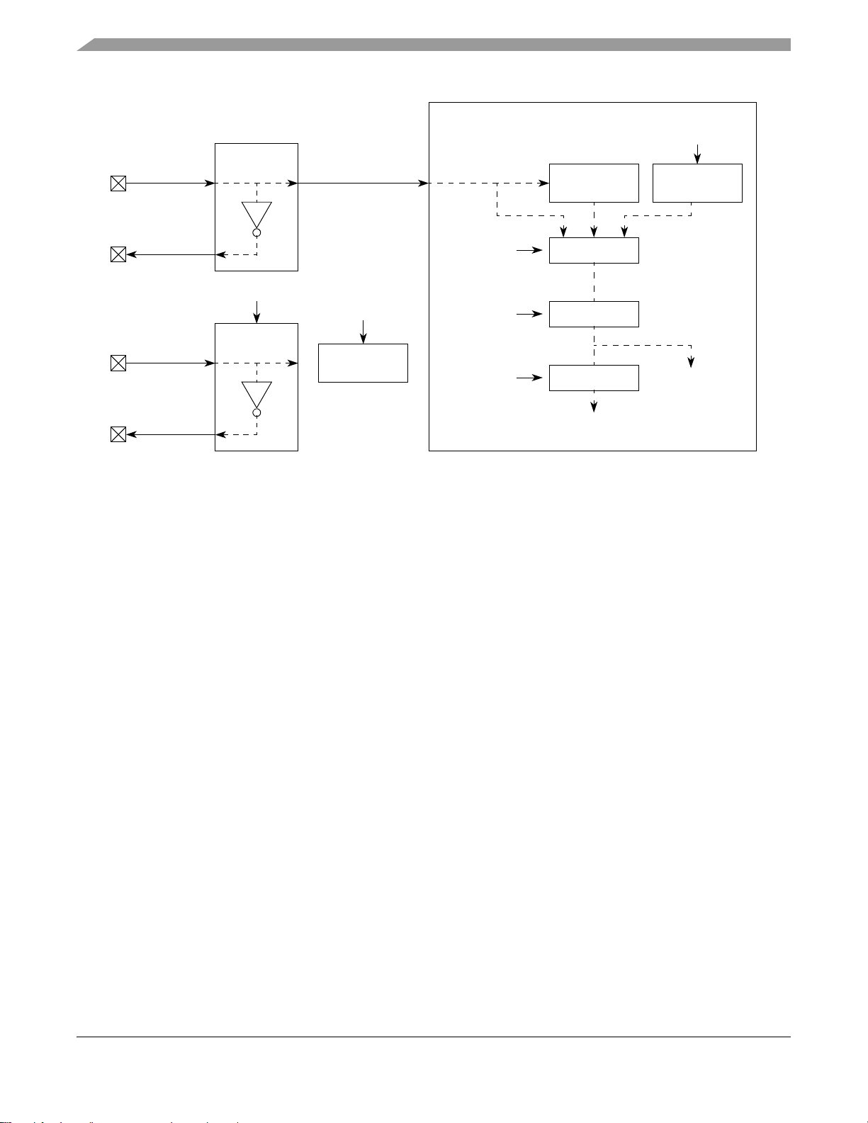
System Clock Description
XOSC
OSCCLK
SYSCLKSEL
2 10
16 MHz
IRC
PLL
Clock
Switcher
+1,2,4,8SYSCLKDIV
+1,2,4,8LPCLKDIV[n]
System Clock
Peripheral Clocks
TRIMIRC
5V3.3 V
EXTAL
3.3 V
XTAL
3.3 V
3.3 V
EXTAL32
5 V
XTAL32
5V
32 kHz
IRC
TRIM32IRC
5V
32 kOSC
OSC32KEN
Figure 3-1. MPC5510 Available Clock Sources
3.2.1 External High-Frequency Crystal (XOSC)
The MPC5510 features an internal automatic level control (ALC) oscillator. The oscillator is designed for
optimal startup margin with typical crystal oscillators. Oscillator power is supplied from its own 3.3 V
PLL supply voltage generated by the voltage regulator to minimize noise. The oscillator provides the
reference clock for the entire chip. As such, it may be used to drive the system clock directly (when the
PLL is bypassed), or as the input reference clock for the PLL.
A square-wave input can also be supplied to the device through the oscillator by connecting the external
clock source to the EXTAL pin with the oscillator operating in external-clock mode.
Features:
• Supports external high-frequency resonator or crystal in the range of f
for reference frequency specification)
• Pierce oscillator
• Two external pins are dedicated for this function (EXTAL, XTAL)
• 40 MHz max required to support FlexRay
• Clock input to PLL
• This clock source is capable of supporting FlexCAN communications (jitter < 0.5%)
• This clock source is capable of supporting FlexRay communications (jitter < 0.5%) (duty
3-2 Freescale Semiconductor
cycle = 50 ± 10%)
MPC5510 Microcontroller Family Reference Manual, Rev. 1
Preliminary
(see MPC5510 data sheet
ref
Page 74

System Clock Description
• Clock for the RTI
• Optional disable
• Enabled by default after reset
3.2.2 External Low-Frequency Crystal (32kXOSC)
The MPC5510 supports an external 32 kHz crystal to provide accurate wake-up and time-keeping
functions.
Features:
• Two external pins required: EXTAL32 and XTAL32
• Supports external low frequency crystal in the range of f
reference frequency specification)
• Option to clock the API to provide a more accurate wakeup
• Option to clock the RTC to provide accurate time keeping
• Powered from 5 V
• Optional disable
(see MPC5510 data sheet for
ref32
3.2.3 Internal High-Frequency RC Oscillator (IRC)
The MPC5510 includes a 16 MHz IRC as the default system clock out of reset.
Features:
• Fast stabilization, enabling fast recovery
• Frequency trimmable for accuracy
• Option to clock software watchdog timer
• Powered from 5 V
• Always enabled except optionally disabled in sleep modes when not being used
3.2.4 Internal Low-Frequency RC Oscillator (32kRC)
The MPC5510 includes a 32 kHz internal RC oscillator that is intended to be used as a highly reliable clock
source during low-power modes.
Features:
• Frequency trimmable for accuracy
• Option to clock the API to provide a wakeup
• Option to clock the RTC to provide time keeping
• Powered from 5 V
• Optionally enabled
MPC5510 Microcontroller Family Reference Manual, Rev. 1
Freescale Semiconductor 3-3
Preliminary
Page 75
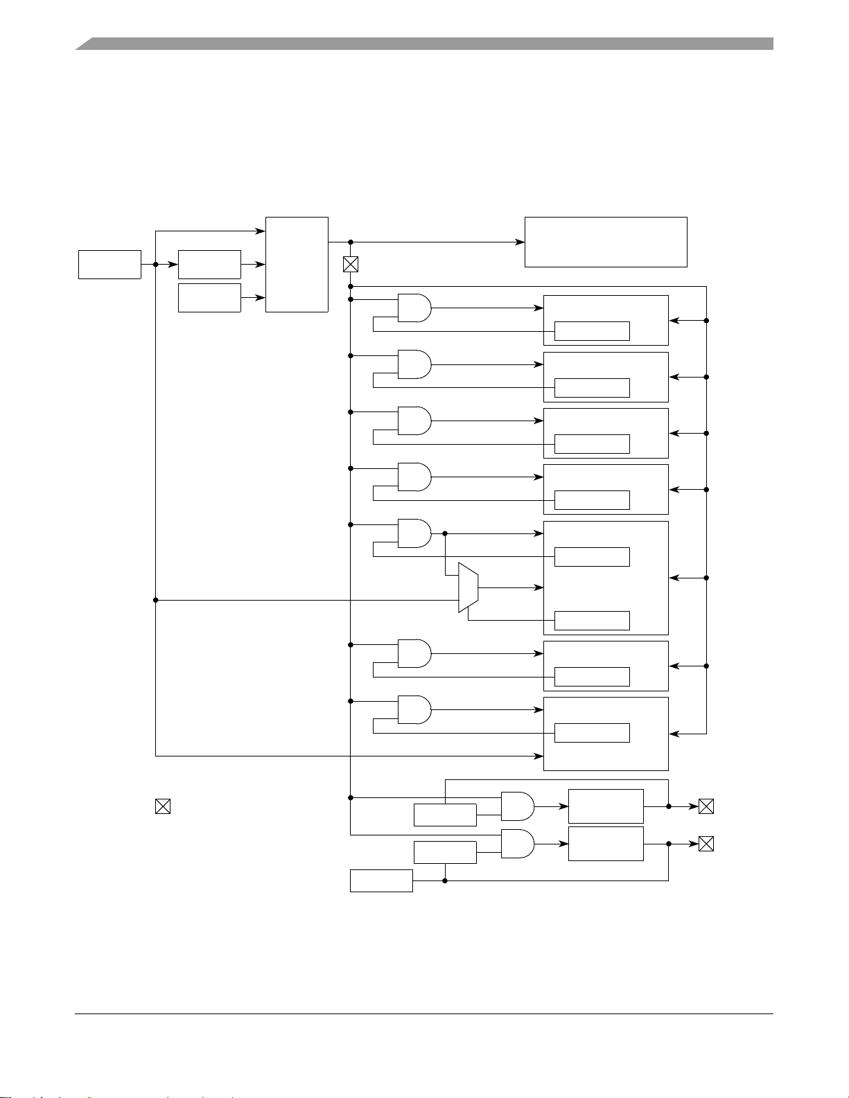
System Clock Description
PLL
IRC
Switcher
and
divider
System clock
XOSC
Cores, INTC, DMA,
SIU, RAM, Flash, BAM,
AIPS, AXBS, MCM
Peripheral dividers
MDIS
DSPI
Module clock
Protocol
clock
MDIS
EBI
MDIS
eMIOS
MDIS
I
2
C/ADC
MDIS
FlexCAN/RAY
CLK_SRC
MDIS
eSCI
MDIS
PIT_RTI
(RTI)
EBI
CLKOUT
divider
CLKOUT
NPC
MCKO
divider
MCKO
Nexus
Oscillator clock
Bypass clock
Selectable peripheral
clock dividers
(div 1,2,4,8)
3.3 System Clock Architecture Block Diagram
To optimize system power consumption, the MPC5510 supports both system- and peripheral-level clock
dividers, and static clock gating using peripheral-level module disable (MDIS) bits and a system-level halt
mechanism. Figure 3-2 shows the device-level clock gating mechanism for the MPC5510.These features
are detailed in subsequent sections.
Figure 3-2. System Clock Architecture
3-4 Freescale Semiconductor
MPC5510 Microcontroller Family Reference Manual, Rev. 1
Preliminary
Page 76

System Clock Description
3.4 Clock Dividers
3.4.1 System Clock Select
The source for the system clock can be selected by the SYSCLKSEL field of the SIU system clock register
(SIU_SYSCLK) to be the 16 MHz IRC, the XOSC, or the PLL.
3.4.2 System Clock Dividers
The system clock dividers can be programmed to create a system clock, which is created from the selected
clock source divided by 1, 2, 4, or 8, based on the setting of the SYSCLKDIV field in the SIU system clock
register (SIU_SYSCLK).
3.4.3 External Bus Clock (CLKOUT) Divider
The external bus clock (CLKOUT) divider can be programmed to create a CLKOUT, which is created
from the system clock divided by 1, 2, or 4, based on the settings of the EBDF bit field in the SIU external
clock control register (SIU_ECCR). The reset value of EBDF selects a CLKOUT frequency of one half of
the system clock frequency. The EBI supports gating of the CLKOUT signal when there are no external
bus accesses in progress.
The CLKOUT divider provides a nominal 50% duty cycle clock. There is no guaranteed phase relationship
between CLKOUT and MCKO.
3.4.4 Nexus Message Clock (MCKO) Divider
The Nexus message clock (MCKO) divider can be programmed to divide the system clock by one, two,
four, or eight based on the MCKO_DIV bit field in the port configuration register (PCR) in the Nexus port
controller (NPC). The reset value of MCKO_DIV selects an MCKO clock frequency one half of the
system clock frequency. The MCKO divider is configured by writing to the NPC through the JTAG port.
The MCKO_EN bit may be used to disable the MCKO clock. The MCKO_GT bit may be used to disable
the MCKO clock when Nexus is not actively transmitting messages on the Nexus port.
The MCKO divider provides a nominal 50% duty cycle clock. There is no guaranteed phase relationship
between CLKOUT and MCKO.
3.4.5 Peripheral Clock Dividers
The peripheral clock dividers provide a mechanism to reduce run power when it is not necessary to clock
peripherals at the full system clock frequency.
MPC5510 Microcontroller Family Reference Manual, Rev. 1
Freescale Semiconductor 3-5
Preliminary
Page 77
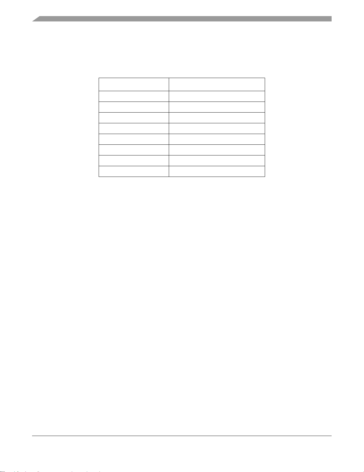
System Clock Description
The SIU’ s SIU_SYSCLK[LPCLKDIVn] bits control the clock divide value for each grouping of modules.
The divide values may be independently selected for each grouping and support a divide by 1, 2, 4, or 8.
Figure 3-1 defines which peripherals are affected by which LPCLKDIVn bits.
Table 3-1. LPCLKDIV Module Groups
LPCLKDIVn Modules
LPCLKDIV0 FlexCAN_A, DSPI_A
2
LPCLKDIV1 ESCI_A, I
LPCLKDIV2 FlexCAN_B-F
LPCLKDIV3 DSPI_B-D
LPCLKDIV4 ESCI_B-H
LPCLKDIV5 eMIOS
LPCLKDIV6 MLB
LPCLKDIV7 Reserved
C_A, PIT
The MPC5510 implements a single clock divider circuit that uses the system clock as its source. The
LPCLKDIV bits control which clock divide tap is used for each module grouping clock gate enable. The
resultant gated clocks will be at the desired frequency but are clock pulses instead of a 50% duty cycle (the
high clock pulse width is half the system clock period). The high-order clock taps will be disabled if not
being used. Individual modules should be disabled when changing the LPCLKDIV values affecting the
module.
The user is responsible for adjusting the module function, prescalers, protocol timings, etc. based on the
LPCLKDIV values. Register accesses will be proportionally longer along with other basic module
functions such as interrupts, DMA, etc.
3.5 Software-Controlled Power Management
3.5.1 Module Disable (MDIS) Clock Gating
Static clock gating is enabled by software writes to configuration bits for the modules to disable the
modules. Modules are re-enabled by software to ungate the module clocks.
The modules support software controlled clock gating where the application software can disable the
non-memory-mapped portions of the blocks by writing to module disable (MDIS) bits in registers within
the blocks. (The memory-mapped portions of the blocks are clocked by the system clock only when they
are accessed.) The Nexus port controller (NPC) can be configured to disable the MCKO signal when there
are no Nexus messages pending. The flash array can be disabled by writing to the STOP bit in the flash’s
module configuration register (MCR).
The modules that support software-controlled power management/clock gating are listed in Table 3-2
along with the registers and bits that disable each block. Default out of reset disables the
software-controlled clocks.
MPC5510 Microcontroller Family Reference Manual, Rev. 1
3-6 Freescale Semiconductor
Preliminary
Page 78
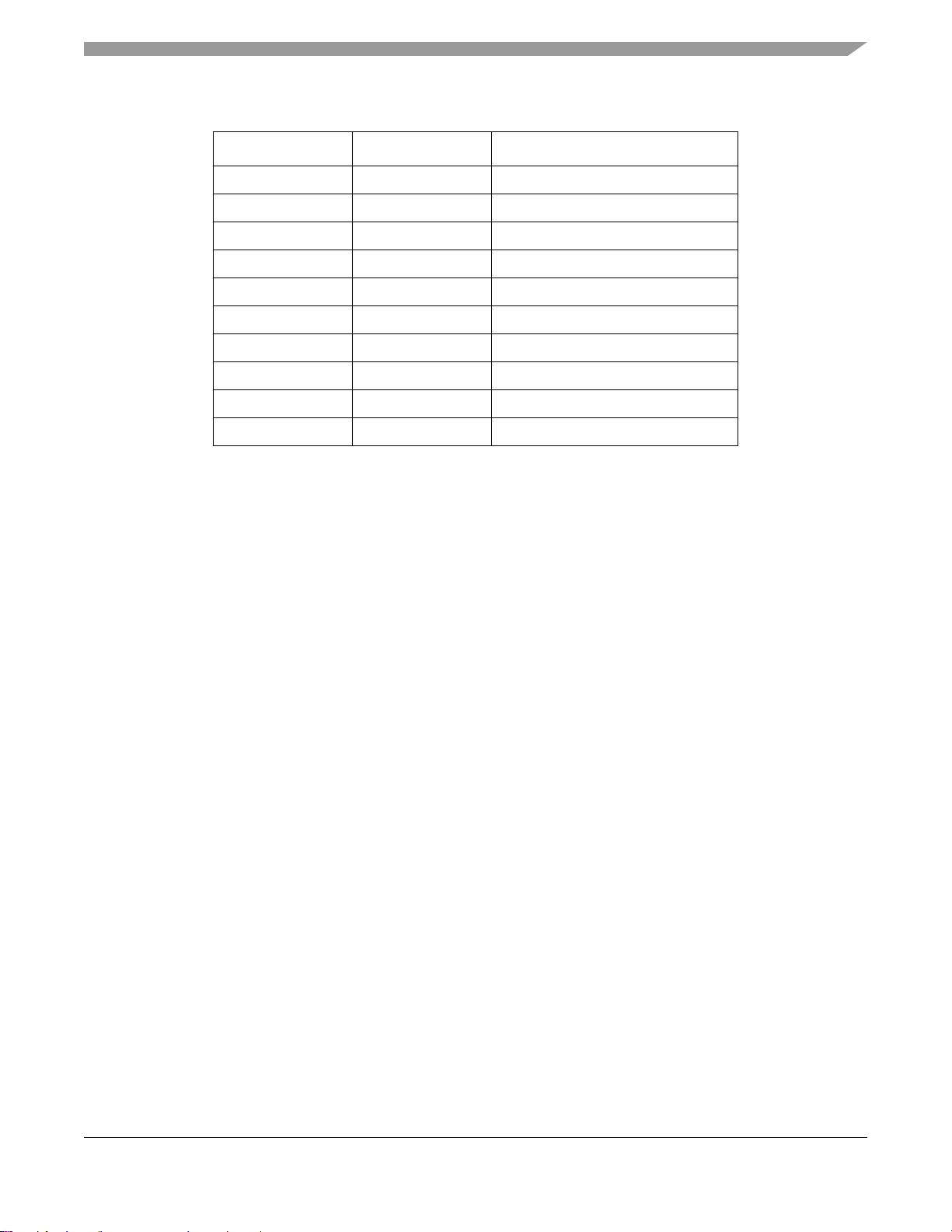
Table 3-2. Software-Controlled Clock Gating Support
Block Name Register Name Bit Name
DSPI MCR MDIS
ESCI MCR MDIS
FlexCAN MCR MDIS
EMIOS MCR MDIS
EBI MCR MDIS
MLB MCR MDIS
PIT_RTI MCR MDIS
2
I
CIBCR MDIS
NPC MCR MCKO_EN, MCKO_GT
Flash Array MCR STOP
1
Only the PIT timers are disabled by MDIS. The RTI is not affected by MDIS.
3.5.2 Halt Clock Gating
System Clock Description
1
System clock gating is forced via the centralized halt mechanism. The SIU_HLT register’s bits
corresponding to individual modules are configured to determine which modules are clock gated.
The HLT bits are used to drive the stop inputs to the modules. After the module completes a clean
shutdown, the module asserts the stop acknowledge handshake. The stop acknowledge is visible in the
SIU_HLTACK read-only register bits. The modules are individually controlled and halted.
The halted module recovers when the HLT bit is cleared by software. After HLT is cleared, the device’s
logic will re-enable the clocks to the modules and negate the stop signal after the required timing has been
met.
There is no hardware disable for the eDMA and FlexRay modules. Thus before setting the HLT bits for
these masters, software should take actions to prepare for the eDMA and FlexRay clocks to be stopped.
Then software sets the HLT bits for the eDMA and FlexRay to indicate to the clock logic that the clocks
to these modules can now be stopped.
When the HLT bits for the eDMA and FlexRay are set and when the Z0 and Z1 have executed WAIT
instructions, then the clocks to the platform are also gated. The platform logic includes the MPU, AXBS,
AIPS, and MCM. The INTC and SIU are not clock gated to allow for an interrupt to be used to exit WAIT.
3.5.3 Core WAIT Clock Gating
Core clock gating is enabled via the CPU WAIT instruction (or, if the core is in reset, by the CRP Core
Reset bit).
The Z1 and Z0 cores may be idled by their WAIT instructions. The WAIT instructions are used as a
power-saving feature to halt the core. Executing the WAIT instruction puts the corresponding core in an
idle state at a clean transition point. When the core stops, clocks to the core are gated off, and the core
MPC5510 Microcontroller Family Reference Manual, Rev. 1
Freescale Semiconductor 3-7
Preliminary
Page 79

System Clock Description
asserts a signal indicating it is waiting for an interrupt. The state of this signal is software accessible via
the appropriate SIU_HLTACK register’s bits.
An interrupt to the corresponding core exits the W AIT instruction and the core co ntinues to the appropriate
interrupt service routine (ISR).
3.6 Alternate Module Clock Domains
3.6.1 FlexCAN Clock Domains
The FlexCAN blocks have two distinct software-controlled clock domains. One of the clock domains is
always derived from the system clock. This clock domain includes the message buffer logic. The source
for the second clock domain can be the system clock or the XOSC output. The logic in the second clock
domain controls the CAN interface pins. The CLK_SRC bit in the FlexCAN CTRL register selects
between the system clock and the oscillator clock as the clock source for the second domain. Selecting the
oscillator as the clock source ensures low jitter on the CAN bus. System software can gate both clocks by
writing to the MDIS bit in the FlexCAN MCR register.
NOTE
To prevent improper FlexCAN behavior when switching of the system
clock or the CAN protocol engine clock source, or before the desired clock
source has stabilized, the FlexCAN module must first be disabled by setting
the FlexCAN_x_MCR[MDIS] = 1.
If the oscillator clock source is selected, the frequency of the peripheral clock needs to be the same or
greater than the oscillator clock frequency.
If the XOSC is used as the system clock source and is divided down, then the clock source selected for the
CAN interface must be the system clock (i.e. divided XOSC) to keep the system clock not slower than the
CAN interface clock.
3.6.2 FlexRay Clock Domains
The FlexRay block has two distinct software-controlled clock domains. One of the clock domains is
always derived from the system clock. The source for the second clock domain can be the system clock or
the XOSC output. The logic in the second clock domain controls the FlexRay interface pins. The
CLK_SRC bit in the FlexRay CTRL register selects between the system clock and the oscillator clock as
the clock source for the second domain. Selecting the oscillator as the clock source ensures low jitter on
the FlexRay bus.
NOTE
To prevent improper FlexRay behavior, the system clock or the FlexRay
protocol engine clock source must be switched and stable before enabling
the FlexRay module. After it is enabled, the FlexRay module can be
disabled only by asserting RESET
.
MPC5510 Microcontroller Family Reference Manual, Rev. 1
3-8 Freescale Semiconductor
Preliminary
Page 80

System Clock Description
If the oscillator clock source is selected for the FlexRay interface, then a divided down XOSC cannot be
selected as the source for the system clock.
3.6.3 RTC Clock Domain
The clock source for the RTC can be selected as one of the following: the 32 kHz IRC, the 32 kHz OSC,
or the 16 MHz IRC.
NOTE
To prevent improper real-time clock (RTC) behavior when switching the
system clock source, or before the desired clock source has stabilized, the
RTC must first be disabled by clearing the CRP_RTCSC[CNTEN] = 0.
3.6.4 SWT Clock Domain
The clock source for the SWT is selectable as the system clock or the 16 MHz IRC.
NOTE
To prevent improper software watchdog timer (SWT) behavior when
switching the system clock source, or before the desired clock source has
stabilized, the SWT must first be disabled by clearing the
MCM_MSWTCR[SWE] = 0.
MPC5510 Microcontroller Family Reference Manual, Rev. 1
Freescale Semiconductor 3-9
Preliminary
Page 81

System Clock Description
MPC5510 Microcontroller Family Reference Manual, Rev. 1
3-10 Freescale Semiconductor
Preliminary
Page 82
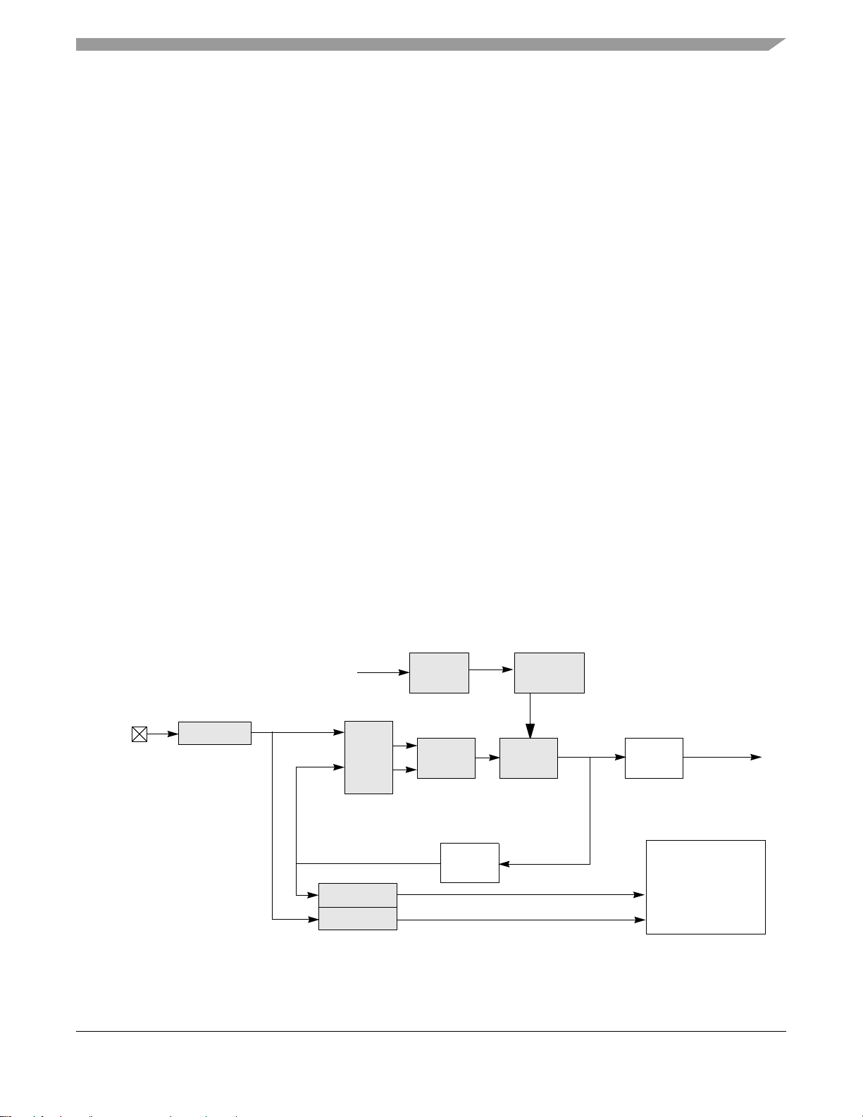
Chapter 4
FMDAC_STEP[0:9]
D2AFM CALDAC
EXTAL
EPREDIV
PFD
FILTER VCO ERFD
LOC_PLL
LOC_REF
EMFD
PLL Clock
Out
Used to create the
loss of clock reset
request and decide
which PLL mode to
switch to when
these things happen
Frequency Modulated Phase Locked Loop (FMPLL)
4.1 Introduction
The FMPLL module is a frequency modulated phase-locked loop that has been optimized to generate
voltage controlled oscillator (VCO) frequencies from 192 MHz to 500 MHz based on an input clock range
of 4 MHz to 40 MHz. The frequency multiplication, output dividers, and the frequency modulation
waveform are register-programmable through a peripheral bus interface.
NOTE
Although this PLL is basically the same PLL that is used on other Power PC
parts, its implementation is different, owing to the use of an internal 16 MHz
IRC, low-power modes, and other features specific to the 5510 family.
4.1.1 Block Diagram
A simplified block diagram of the FMPLL illustrates the functionality and interdependence of major
blocks (see Figure 4-1). Shaded blocks represent analog circuit components that make up the core analog
portion of the FMPLL. The complete FMPLL closed-loop system contains the feedback divider (EMFD)
and output divider (ERFD), which are implemented with standard cell core logic elements. Refer to
Section 4.4.3.3, “PLL Normal Mode Without FM,” for details on each sub-block.
MPC5510 Microcontroller Family Reference Manual, Rev. 1
Freescale Semiconductor 4-1
Figure 4-1. FMPLL Block Diagram
Preliminary
Page 83

Frequency Modulated Phase Locked Loop (FMPLL)
4.1.2 Features
The FMPLL has these major features:
• Input clock frequency range: 4 MHz to 40 MHz (EXTAL pin)
• Because the MPC5510 uses a 16 MHz IRC as its default system clock, the FMPLL will be put in
PLL Off mode during reset, so that power dissipation is minimized by disabling the FMPLL until
needed by the system.
• Programmable frequency multiplication factor settings generating VCO frequencies of
192 MHz – 500 MHz
• PLL Off mode (low-power stop)
• Register programmable output clock divider (ERFD)
• Programmable frequency modulation
— Modulation applied as a triangle waveform
— Peak-to-peak register programmable modulation depths of 0.5%, 1%, 1.5%, and 2% of the
system frequency
— Register programmable modulation rates of F
extal
/80, F
/40, and F
extal
extal
/20
• Lock detect circuitry provides a signal indicating the FMPLL has acquired lock and continuously
monitors the FMPLL output for any loss of lock
• Loss-of-clock circuitry monitors input reference and FMPLL output clocks with programmable
ability to select a backup clock source as well as generate a reset or interrupt in the event of a failure
4.1.3 Modes of Operation
There are two main modes of FMPLL: PLL Off mode and normal mode. These modes are briefly described
in this section.
When PLL Off mode is selected, the FMPLL is off, and the end-system user must have selected a dif ferent
SIU MUX source than the PLL Output. The lock detector is not functional and will not indicate that the
FMPLL is in a locked state. Frequency modulation is not available and the FMPLL is put into a low-power,
idle state. This operating mode is described in Section 4.4.2, “PLL Off Mode.”
When normal mode is selected, the FMPLL is fully programmable. The FMPLL reference clock source
can be a crystal oscillator or an external clock generator. The lock detector will function and indicate the
lock status of the FMPLL and frequency modulation of the output clock can be enabled. This operating
mode is described in Section 4.4.3, “Normal Mode.”
4.2 External Signal Description
Refer to Table 2-1 and Section 2.7, “Detailed External Signal Descriptions,” for detailed signal
descriptions.
4.3 Memory Map and Registers
This section provides a detailed description of all FMPLL registers.
MPC5510 Microcontroller Family Reference Manual, Rev. 1
4-2 Freescale Semiconductor
Preliminary
Page 84
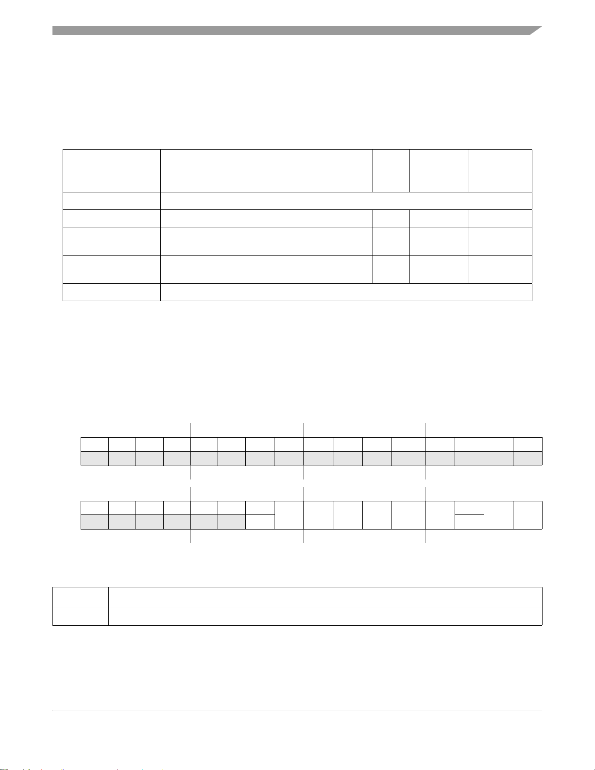
Frequency Modulated Phase Locked Loop (FMPLL)
4.3.1 Module Memory Map
Table 4-1 shows the FMPLL memory map. The address of each register is given as an offset to the FMPLL
base address. Registers are listed in address order, identified by complete name and mnemonic, and lists
the type of accesses allowed.
Table 4-1. FMPLL Memory Map
Offset from
FMPLL_BASE_ADDR
(0xFFFF_0000)
0x0000 Reserved
0x0004 SYNSR—FMPLL Synthesizer Status Register R/W —
Register Access Reset Value Section/Page
1
4.3.2.1/4-3
0x0008 ESYNCR1—FMPLL Enhanced Synthesizer Control
Register 1
0x000C ESYNCR2—FMPLL Enhanced Synthesizer Control
Register 2
0x0010–0x0014 Reserved
1
See specific register description.
R/W 0x8001_0053 4.3.2.2/4-5
R/W 0x0000_0005 4.3.2.3/4-8
4.3.2 Register Descriptions
This section lists the FMPLL registers in address order and describes the registers and their bit fields.
4.3.2.1 FMPLL Synthesizer Status Register (SYNSR)
FMOffset: PLL_BASE_ADDR + 0x0004 Access: User read/write
0 1 2 3 4 5 6 7 8 9 10 11 12 13 14 15
R 0 0 0 0 0 0 0 0 0 0 0 0 0 0 0 0
W
Reset00000000 0 00 0 00 00
16 17 18 19 20 21 22 23 24 25 26 27 28 29 30 31
R 0 0 0 0 0 0LOLF
W
Reset00000000 0 00 0 00 00
LOC MODE
w1c w1c
PLL
SEL
PLL
REF
LOCKS LOCK
LOCF
CAL
DONE
CAL
PASS
Figure 4-2. FMPLL Synthesizer Status Register (SYNSR)
Table 4-2. SYNSR Register Field Descriptions
Field Description
bits 0–21 Reserved.
MPC5510 Microcontroller Family Reference Manual, Rev. 1
Freescale Semiconductor 4-3
Preliminary
Page 85

Frequency Modulated Phase Locked Loop (FMPLL)
Table 4-2. SYNSR Register Field Descriptions (continued)
Field Description
LOLF Loss- of-Lock Flag. This bit provides the interrupt request flag. To clear the flag, write a 1 to the bit. Writing 0 has
no effect. This flag will not be set, and an interrupt will not be requested, if the loss-of-lock condition was caused
by a system reset, enabling frequency modulation, or write to the ESYNCR1 which modifies the
ESYNCR1[EMFD] bits. If the flag is set due to a system failure, writing the ESYNCR1[EMFD] bits or enabling FM
will not clear the flag. Assert reset to clear the flag. If lock is reacquired, the bit will remain set until either a write
1 or reset is asserted.
1 Inter rupt service requested
0 Inte rrupt service not requested
LOC Loss-Of-Clock Status. The LOC bit is an indication of whether a loss-of-clock condition is present when operating
in normal PLL mode. If LOC=0, the system clocks are operating normally . If LOC=1, the system clocks have failed
due to a reference failure or a PLL failure. If the read of the LOC bit and the loss-of-clock condition occur
simultaneously , the bit does not reflect the current loss-of-clock condition. If a loss-of-cloc k condition occurs that
sets this bit and the clocks later return to normal, this bit will be cleared. LOC is always zero in PLL Off mode.
1 Clo cks are not operating normally
0 Clocks are operating normally
MODE Clock Mode. The initial value for the MODE bit is determined at reset. The state of this bit, along with PLLSEL
and PLLREF, indicates which clock mode the PLL is operating in (see Table 4-3). The value of
ESYNCR1[CLKCFG0] will be reflected in this location.
1 PLL clock mode
0 PLL Off mode
PLLSEL PLL Mode Select. The initial value for the PLLSEL bit is determined at reset. The state of this bit, alon g with
MODE and PLLREF, indicates which mode the PLL operates in (see Table 4-3). This bit is cleared in PLL Off
mode. The value of ESYNCR1[CLKCFG1] will be reflected in this location.
1 Normal PLL mode
0 PLL Off mode
PLLREF PLL Clock Reference Source. The initial value for the PLLREF bit is determined at reset. The state of this bit,
along with MODE and PLLSEL, indicates which reference source has been chosen for normal PLL mode (see
Table 4-3). This bit is cleared in PLL Off mode. The value of ESYNCR1[CLKCFG2] will be reflected in this
location.
1 Crystal clock reference chosen
0 Exte rnal clock reference chosen
Note: User must also use the XOSC bit in the CRP register (CRP_CLKSRC) to enable the 4 to 40 MHz oscillator.
LOCKS Sti cky PLL Lock Status Bit. The LOCKS bit is a sticky indication of PLL lock status. LOCKS is set by the lock
detect circuitry when the PLL acquires lock after: 1) a system reset, or 2) a write to the ESYNCR2 which modifies
the ESYNCR2[EMFD] bits, or 3) frequency modulation is enabled. Whenever the PLL loses lock, LOCKS is
cleared. LOCKS remains cleared after the PLL re-locks, until one of the three conditions occurs. Furthermore, if
the LOCKS bit is read when the PLL simultaneously loses lock, the bit does not reflect the current loss-of-lock
condition.
If operating in PLL Off mode, LOCKS remains cleared after reset.
1 PLL ha s not lost lock since last system reset, a write to ESYNCR1 to modify the ESYNCR1[EMFD] bit field,
or frequency modulation enabled
0 PLL ha s lost lock since last system reset, a write to ESYNCR1 to modify the ESYNCR1[EMFD] bit field, or
frequency modulation enabled
MPC5510 Microcontroller Family Reference Manual, Rev. 1
4-4 Freescale Semiconductor
Preliminary
Page 86
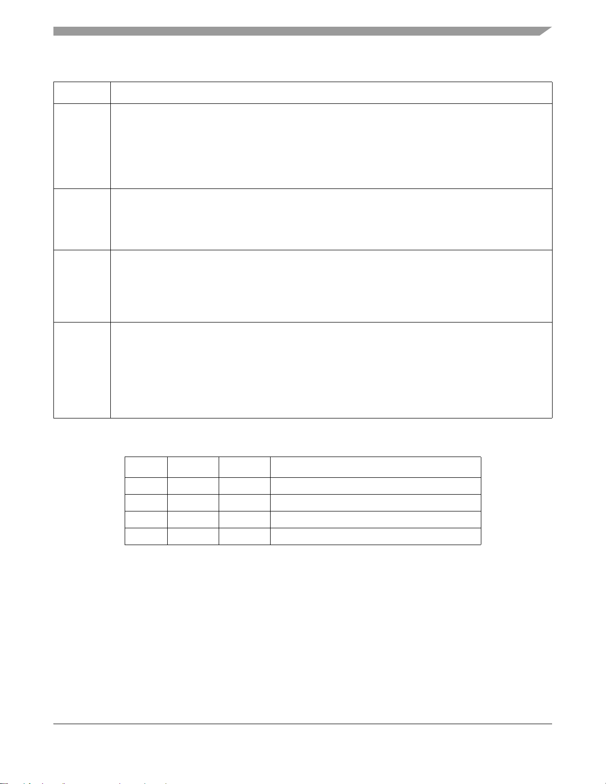
Frequency Modulated Phase Locked Loop (FMPLL)
Table 4-2. SYNSR Register Field Descriptions (continued)
Field Description
LOCK PLL Lock Status Bit. The LOCK bit indicates whether the PLL has acquired lock. PLL lock occurs when the
synthesized frequency matches to within approximately 0.75% of the programmed frequency . The PLL loses lock
when a frequency deviation of greater than approximately 1.5% occurs. If the LOCK bit is read when the PLL
simultaneously loses lock or acquires lock, the bit does not reflect the current condition of the PLL.
If operating in PLL Off mode, LOCK remains cleared after reset.
1 PLL is locked
0 PLL is unlocked
LOCF Loss-of-Clock Flag. This bit provides the interrupt request flag. To clear the flag, write a 1 to the bit. Writing 0 has
no effect. Asserting reset will clear the flag. If clocks return to normal after the flag has been set, the bit will remain
set until cleared by either writing 1 or asserting reset. A loss-of-clock condition can only be detected if LOCEN=1.
1 Inter rupt service requested
0 Inte rrupt service not requested
CALDONE Cal ibrati on Complete. The CALDONE bit is an indication of whether the calibration sequence has been
completed since the last time modulation was enabled. If CALDONE=0 then the calibration sequence is in
progress or modulation is disabled. If CALDONE=1 then the calibration sequence has been completed, and
frequency modulation is operating.
1 Calibration complete
0 Cal ibration not complete
CALPASS Calibration Passed. The CALPASS bit tells whether the calibration routine was successful. If CALPASS=1 and
CALDONE=1 then the routine was successful. If CALPASS=0 and CALDONE=1, then the routine was
unsuccessful. When the calibration routine is initiated the CALPASS is asserted. CALPASS remains asserted
until modulation is disabled by clearing the EDEPTH bits in the ESYNCR2 register or a failure occurs within the
FMPLL calibration sequence.
1 Calibration successful
0 Calibration unsuccessful
If calibration is unsuccessful, then actual depth is not guaranteed to match the desired depth
MODE PLLSEL PLLREF Clock Mode
0 X X PLL Off mode
10 0Reserved
1 1 0 Normal PLL mode with external clock reference
1 1 1 Normal PLL mode with crystal clock reference
Table 4-3. System Clock Status Per Mode
4.3.2.2 FMPLL Enhanced Synthesizer Control Register 1 (ESYNCR1)
This is one of two FMPLL synthesizer control registers that are used to access enhanced features in the
FMPLL. The bit fields in the ESYNCR1 behave as described in Figure 4-3.
MPC5510 Microcontroller Family Reference Manual, Rev. 1
Freescale Semiconductor 4-5
Preliminary
Page 87
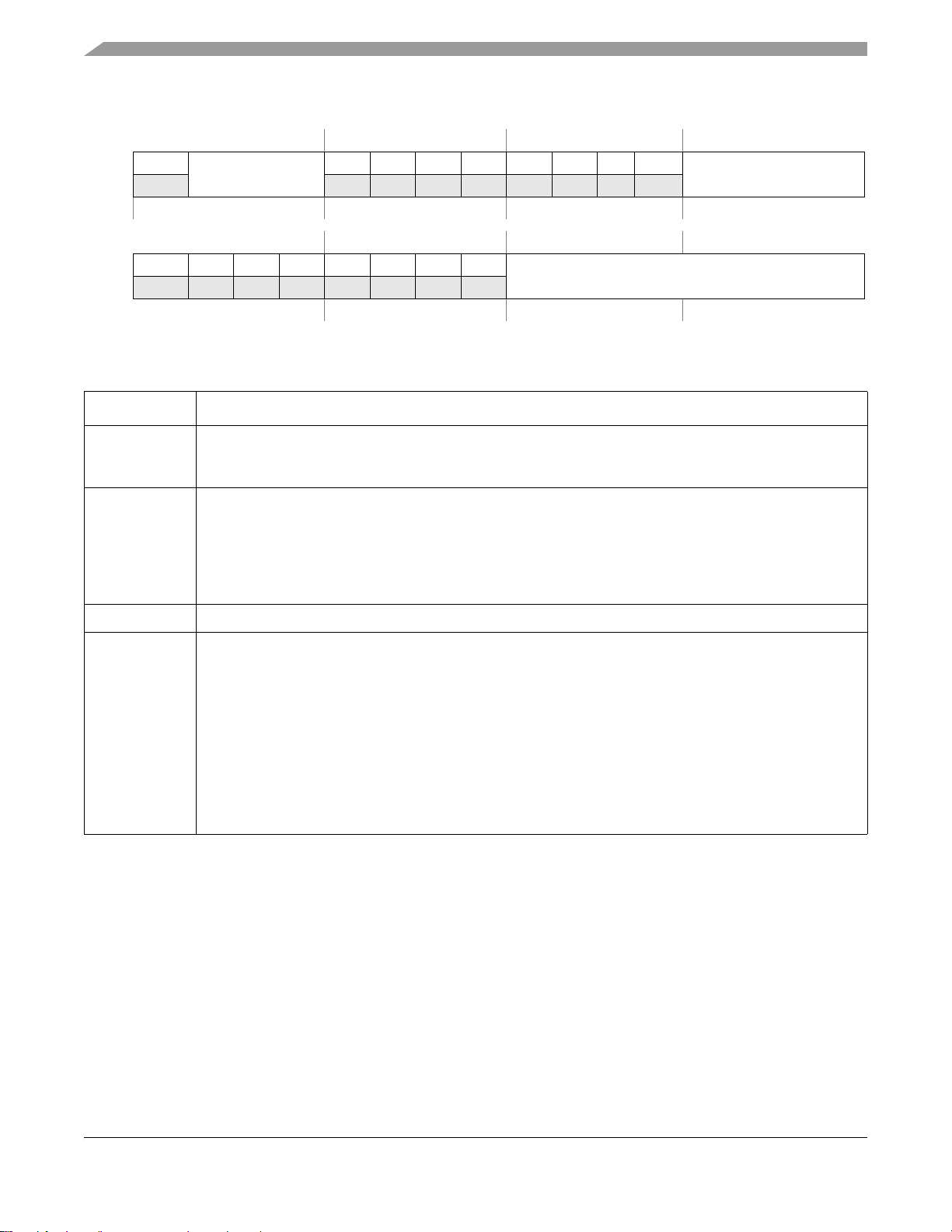
Frequency Modulated Phase Locked Loop (FMPLL)
FMOffset: PLL_BASE_ADDR + 0x0008 Access: User read/write
0 123456789101112131415
R 1
W
CLKCFG[0:2]
0 0 0 0 0 0 0 0
EPREDIV
Reset1 000000000000001
16 17 18 19 20 21 22 23 24 25 26 27 28 29 30 31
R 0 0 0 0 0 0 0 0
W
EMFD
Reset0 000000001010011
Figure 4-3. FMPLL Enhanced Synthesizer Control Register 1 (ESYNCR1)
Table 4-4. ESYNCR1 Register Field Descriptions
Field Description
bit 0 Reserved.
Note: This bit is set to 1 on reset and always reads as 1.
CLKCFG[0:2] Clock Configuration. The CLKCFG[0:2] bits are writable versions of the MODE, PLLSEL, and PLLREF bits
in the SYNSR. These change the clock mode, after reset has negated, via software. CLKCFG[0:2] map
directly to MODE, PLLSEL, and PLLREF to control the system clock mode (see Table 4-3).
Note: CLKCFG[0:2] = 0b101 can produce an unpredictable clock output.
Note: The ESYNCR2[LOLRE] and ESYNCR2[LOCRE] should be set to 0 before changing the PLL mode, so
that a reset is not immediately generated upon the write to CLKCFG[0:2]
bits 4–11 Reserved.
EPREDIV Enhanced Pre-Divider. The EPREDIV bits control the value of the divider on the input clock. The output of
the pre-divider circuit generates the reference clock to the PLL analog loop. The decimal equivalent of the
EPREDIV binary number is substituted into the equation from Table 4-11.
Note: Setting the EPREDIV to any of the invalid states in Table 4-5 will cause the PLL to produce an
unpredictable output clock. and the output frequency of the divider must equal the PLL reference
frequency, f
(see MPC5510 data sheet).
pllref
When the EPREDIV bits are changed, the PLL will immediately lose lock. If the EPREDIV bits are changed
during FM calibration, the current calibration sequence is terminated and the DEPTH bits are cleared. The
PLL will re-lock to the new EPREDIV value you must manually re-enable modulation. To prevent an
immediate reset, clear the LOLRE bit before writing the EPREDIV bits. In PLL Off mode the EPREDIV bits
have no affect. The available enhanced pre-divider ratios are given in Table 4-5.
MPC5510 Microcontroller Family Reference Manual, Rev. 1
4-6 Freescale Semiconductor
Preliminary
Page 88
Frequency Modulated Phase Locked Loop (FMPLL)
Table 4-4. ESYNCR1 Register Field Descriptions (continued)
Field Description
bits 16–23 Reserved.
EMFD Enhanced Multiplication Factor Divider. The EMFD bits control the value of the divider in the PLL feedback
loop. The value specified by the EMFD bits establish the multiplication factor applied to the reference
frequency. The decimal equivalent of the EMFD binary number is substituted into the equation from
Table 4-11 for F
to determine the equivalent multiplication factor. The range of settings is
sys
32 ≤ EMFD ≤ 132.
Note: EMFD values less than 32 and greater than 132 are invalid and will cause the PLL to produce an
unpredictable clock output. The VCO frequency must be within the f
specification (see MPC5510
vco
data sheet)
When the EMFD bits are changed, the PLL loses lock.If the EMFD bits are changed during FM calibration,
the current calibration sequence is terminated and the DEPTH bits are cleared. The PLL will re-lock to the
new EMFD value you must manually re-enable modulation. To prevent an immediate reset, clear the LOLRE
bit before writing the EMFD bits.
In PLL Off mode the EMFD bits have no affect.
Table 4-6 shows the available divide ratios.
Table 4-5. Enhanced Pre-divider Ratios
EPREDIV Input Divide Ratio (EPREDIV+1)
0000 1
0001 2 (default for MPC5510)
0010 3
0011 4
0100 5
0101 6
0110 Invalid
0111 8
1000 Invalid
1001 10
1010–1111 Invalid
Table 4-6. Enhanced Feedback Divide Ratios
EMFD Feedback Divide Ratio (EMFD+16)
0000_0000–0001_1111 Invalid
0010_0000 48
0010_0001 49
0010_0010 50
0010_0011 51
0010_0100 52
MPC5510 Microcontroller Family Reference Manual, Rev. 1
Freescale Semiconductor 4-7
Preliminary
Page 89
Frequency Modulated Phase Locked Loop (FMPLL)
Table 4-6. Enhanced Feedback Divide Ratios
EMFD Feedback Divide Ratio (EMFD+16)
0010_0101 53
.
.
0101_0011
.
.
1000_0100 148
1000_0101–1111_1111 Invalid
99 (default for MPC5510)
.
.
.
.
4.3.2.3 FMPLL Enhanced Synthesizer Control Register 2 (ESYNCR2)
This is the second of two enhanced versions of the FMPLL synthesizer control register used to access
enhanced features in the FMPLL. The bit fields in the ESYNCR2 behave as described in Figure 4-4.
FMOffset: PLL_BASE_ADDR + 0x000C Access: User read/write
01234567 8 9 101112131415
R 0 0 0 0 0 0 0 0
W
Reset00000000 0 0 0 00000
LOCEN LOLRE LOCRE
LOL
IRQ
LOC
IRQ
0
ERATE
16 17 18 19 20 21 22 23 24 25 26 27 28 29 30 31
R 0 0 0 0 0
W
Reset00000000 0 0 0 0 0 1 0 1
EDEPTH
0 0
ERFD
Figure 4-4. FMPLL Enhanced Synthesizer Control Register 2 (ESYNCR2)
Table 4-7. ESYNCR2 Field Descriptions
Field Description
bits 0–7 Reserved.
LOCEN Loss-of-Clock Enable. The LOCEN bit determines whether the loss-of-clock function is operational along with
backup clock modes, and interrupt and reset functions. See Section 4.4.3.2, “Loss-of-Clock Detection,” for
more information.
In PLL Off mode, this bit has no affect.
LOCEN does not affect the loss-of-lock circuitry.
1 Loss-of-clock enabled.
0 Loss-of-clock disabled.
LOLRE Loss-of-Lock Reset Enable. The LOLRE bit determines how the integration module handles a loss-of-lock
indication. See Section 4.4.3.1, “PLL Lock Detection,” for more information.
When operating in normal PLL mode, the PLL must be locked before setting the LOLRE bit. Otherwise reset
is immediately asserted.
The LOLRE bit has no affect in PLL Off mode.
1 Assert reset on loss of lock enabled.
0 Assert reset on loss of lock disabled.
MPC5510 Microcontroller Family Reference Manual, Rev. 1
4-8 Freescale Semiconductor
Preliminary
Page 90

Frequency Modulated Phase Locked Loop (FMPLL)
Table 4-7. ESYNCR2 Field Descriptions (continued)
Field Description
LOCRE Loss-of-Clock Reset Enable. The LOCRE bit determines how the integration module handles a loss-of-clock
condition when LOCEN is equal to 1. LOCRE has no effect when LOCEN is equal to 0.
If the LOCF bit in the SYNSR indicates a loss-of-clock condition, setting the LOCRE bit causes an immediate
reset.
In PLL Off mode LOCRE has no affect.
1 Assert reset on loss of clock enabled
0 Assert reset on loss of clock disabled.
LOLIRQ Loss-of-Lock Interrupt Request. The LOLIRQ bit determines how the integration module handles a
loss-of-lock indication. See Section 4.6.1, “Loss-of-Lock Interrupt Request,” for more information.
When operating in normal mode, the PLL must be locked before setting the LOLIRQ bit. Otherwise an
interrupt is immediately requested.
The LOLIRQ bit has no affect in PLL Off mode.
1 Request interrupt enabled
0 Request interrupt disabled
LOCIRQ Loss- of-Clock Interrupt Request. The LOCIRQ bit determines how the integration module handles a loss-
of-clock condition when LOCEN=1. LOCIRQ has no effect when LOCEN=0.
If the LOCF bit in the SYNSR indicates a loss-of-clock condition, setting (or having previously set) the
LOCIRQ bit causes an interrupt request.
In PLL Off mode LOCIRQ has no affect.
1 Request interrupt on loss of clock enabled.
0 Request interrupt on loss of clock disabled
bit 13 Reserved.
ERATE Enhanced Modulation Rate. The ERATE bits control the rate of frequency modulation applied to the system
frequency. Table 4-8 shows the allowable modulation rates.
bits 16–20 Reserved.
EDEPTH Enhanced Modulation Depth. The EDEPTH bit field controls the frequency modulation depth and enables the
frequency modulation. When programmed to a value other than 0x0 the frequency modulation is
automatically enabled. Table 4-9 shows are the programmable frequency deviations from the system
frequency . Upon a change in the depth value to other than 0x0, the calibration sequence will be re initialized.
bits 24–25 Reserved.
ERFD Enhanced Reduced Frequency Divider. The ERFD bits control a divider at the output of the PLL. The value
specified by the ERFD bits establish the divisor applied to the PLL frequency. The ERFD divides the output
clock by the quantity (ERFD + 1). Even-numbered RFD settings , which would result in odd divide ratios, are
not allowed.
The decimal equivalent of the ERFD binary number is substituted into the equation from Table 4-11.
Note: The ERFD divides the output clock by the quantity (ERFD + 1). Even numbered ERFD settings, which
would result in odd divide ratios, are invalid and cause the PLL to produce an unpredictable output
clock. The PLL output clock must be within the f
specification (see MPC5510 data sheet).
pll
Changing the ERFD bits does not affect the PLL, hence, no re-lock delay is incurred. Resulting changes in
clock frequency are synchronized to the next falling edge of the current system clock. These bits should be
written only when the lock bit (LOCK) is set, to avoid surpassing the allowable system operating frequency.
In PLL Off mode the ERFD bits have no affect.
The available enhanced output divider ratios are given in Table 4-10.
MPC5510 Microcontroller Family Reference Manual, Rev. 1
Freescale Semiconductor 4-9
Preliminary
Page 91
Frequency Modulated Phase Locked Loop (FMPLL)
Table 4-8. Programmable Modulation Rates
ERATE Modulation Rate (Hz)
00 F
01 F
10 F
mod
mod
mod
= F
= F
= F
extal
extal
extal
/80
/40
/20
11 Invalid
Table 4-9. Programmable Modulation Depths
EDEPTH Modulation Depth (% of F
000 0
001 0.25% – 0.5%
010 0.75% – 1.0%
011 1.25% – 1.5%
100 1.75% – 2.0%
101 – 111 Reserved
sys
Table 4-10. Enhanced Output Divide Ratios
ERFD Output Divide Ratio (ERFD+1)
00_0000 1
)
00_0001 2
00_0010 Invalid
00_0011 4
00_0100 Invalid
00_0101 6 (default value for MPC5510)
00_0110 Invalid
00_0111 8
.
.
.
.
.
.
11_1100 Invalid
11_1101 62
11_1110 Invalid
11_1111 64
MPC5510 Microcontroller Family Reference Manual, Rev. 1
4-10 Freescale Semiconductor
Preliminary
Page 92
Frequency Modulated Phase Locked Loop (FMPLL)
F
sys
F
extal
EMFD 16+()•
EPREDIV 1+()ERFD 1+()
---------------------------------------------------------------------------=
4.4 Functional Description
The FMPLL module contains the frequency modulated phase lock loop (FMPLL), enhanced frequency
divider (ERFD), enhanced synthesizer control registers (ESYNCR1 and ESYNCR2), synthesizer status
register (SYNSR), and clock/PLL control logic. The block also contains a reference frequency pre-divider
controlled by the EPREDIV bits in the ESYNCR1. This enables the user to use a high frequency crystal
or external clock generator and obtain finer frequency synthesis resolution than would be available if the
raw input clock were used directly by the analog loop. For the remainder of this chapter, the term
“reference frequency” and the symbol F
on which frequency multiplication will be performed.
4.4.1 General
At reset, the system clock is driven by the internal oscillator (16 MHz IRC) and the module is in bypass
mode. After reset, software can change the PLL mode (see Section 4.5.1, “Clock Mode Selection”).
Table 4-11 shows the PLL-clock to input-clock frequency relationships for the available clock modes.
Table 4-11. Clock-Out vs. Clock-In Relationships
Clock Mode Frequency Equation
indicate the output of the pre-divider circuit. This is the clock
ref
Normal PLL Mode
4.4.2 PLL Off Mode
When PLL Off mode is selected, the PLL is off and either the 16 MHz IRC must be selected as the system
clock or the user must supply an external clock or crystal on the EXTAL pin, and select that clock source
before entering PLL Off mode. The selected clock is directly used to produce the various system clocks.
Refer to MPC5510 Microcontroller Family Data Sheet for external clock input requirements. In bypass
mode, the analog portion of the PLL is disabled, the frequency modulation capability is not available, and
no clocks are generated at the PLL output. The pre-divider is bypassed and has no effect on the system
clock frequency in bypass mode.
4.4.3 Normal Mode
When normal PLL mode is selected, the PLL is fully programmable. The PLL can synthesize frequencies
ranging from 48x to 148x the reference frequency of the output of the predivider. with or without
frequency modulation enabled. The post-divider is capable of reducing the PLL clock frequency without
forcing a re-lock. The PLL reference can be a crystal oscillator reference or an external clock reference.
This clock will be divided by the pre-divider circuit to create the PLL reference clock.
4.4.3.1 PLL Lock Detection
The lock detect logic monitors the reference frequency and the PLL feedback frequency to determine when
frequency lock has been achieved. Phase lock is inferred by the frequency relationship, but is not
MPC5510 Microcontroller Family Reference Manual, Rev. 1
Freescale Semiconductor 4-11
Preliminary
Page 93
Frequency Modulated Phase Locked Loop (FMPLL)
Count N + K
Reference cycles,
and compare
number of feed-
Lock detected
back cycles
Relax lock
criteria.
Reference count
equals N and feedback count equals N
in same count and
compare sequence.
Reference count
equals N + K and feedback count equals N + K
in same count and
compare sequence.
Alert system that
PLL has locked.
Feedback count does not
equal reference count of N or
N+K. Alert system that PLL
is not locked. Tighten
lock criteria.
Continue
monitoring PLL
with alternate
N and N+K count
and compare
sequences.
Count N
reference cycles,
and compare
number of feedback
cycles elapsed.
elapsed.
guaranteed. The PLL lock status is reflected in the LOCK status bit in the SYNSR. A sticky lock status
indication, LOCKS, is also provided.
The lock detect function uses two counters, which are clocked by the reference and PLL feedback
respectively . When the reference counter has counted N cycles, the feedback counter’s count is compared.
If the feedback counter has also counted N cycles, the process is repeated for N + K counts. Then if the
two counters’ counts match, the lock criteria is relaxed by one count and the system is notified that the
PLL has achieved frequency lock. Then takes three successful compares before tolerance is relaxed.
After lock has been detected, the lock circuitry continues to monitor the reference and feedback
frequencies using the alternate count and compare process. If the counters do not match at any comparison
time, then the LOCK status bit is cleared to indicate that the PLL has lost lock. At this point, the lock
criteria is tightened and the lock detect process is repeated.
The alternate count sequences prevent false lock detects due to frequency aliasing while the PLL tries to
lock. Alternating between a tight and relaxed lock criteria prevents the lock detect function from randomly
toggling between locked and not locked status due to phase sensitivities. Figure 4-5 illustrates the
sequence for detecting locked and not-locked conditions.
When the frequency modulation is enabled, the loss of lock continues to function as described but with the
lock and loss of lock criteria reduced to ensure that false loss of lock conditions are not detected.
In PLL Off mode, the PLL cannot lock because the PLL is disabled.
Figure 4-5. Lock Detect Sequence
4-12 Freescale Semiconductor
MPC5510 Microcontroller Family Reference Manual, Rev. 1
Preliminary
Page 94
Frequency Modulated Phase Locked Loop (FMPLL)
After the PLL acquires lock after reset, the LOCK and LOCKS status bits are set. If the EPREDIV or
EMFD are changed, or if an unexpected loss-of-lock condition occurs, the LOCK and LOCKS status bits
are negated. While the PLL is in an unlocked condition, the system clocks continue to be sourced from the
PLL as the PLL attempts to re-lock. Consequently, during the re-locking process, the system clock
frequency is not well defined and may exceed the maximum system frequency violating the system clock
timing specifications. Because of this condition, using the loss-of-lock reset function is recommended.
After the PLL has re-locked, the LOCK bit is set. The LOCKS bit remains cleared if the loss of lock was
unexpected. The LOCKS bit is set to one when the loss of lock was caused by changing the EPREDIV or
EMFD fields.
4.4.3.2 Loss-of-Clock Detection
When enabled by the LOCEN bit in the ESYNCR2, the loss-of-clock (LOC) detection circuit monitors the
input clocks to the phase/frequency detector (PFD) (see Figure 4-1). When the reference or feedback clock
frequency falls below a minimum frequency, the LOC circuitry considers the clock to have failed and a
loss-of-clock status is reflected by the sticky LOCF bit, and non-sticky LOC bit in the SYNSR. See
MPC5510 Microcontroller Family Data Sheet for the minimum clock frequency. In PLL Off mode, the
loss-of-clock circuitry is disabled.
Depending on which clock source has failed, the LOC circuitry switches the PLL’s output clock source to
the remaining operational clock, if enabled by LOCEN. The PLL’s output clocks are derived from the
alternate clock source until reset is asserted. If the reference fails, the PLL goes out of lock and into
self-clocked mode (SCM) (see Table 4-12). The PLL remains in SCM until the next reset. When the PLL
is operating in SCM, the PLL will run open loop at a default VCO frequency. The RFD will set to
divide-by-4 to ensure the clock presented to the system will be well below the maximum allowable
frequency for the device. If the loss-of-clock condition is due to a PLL failure (i.e., loss of feedback clock),
the PLL reference becomes the system clocks source until the next reset, even if the PLL regains itself and
re-locks.
Table 4-12. Loss-of-Clock Summary
System Clock
Clock Mode
PLL PLL PLL self-clocked mode PLL reference
PLL bypass Ext. Clock(s) None NA
Note: The LOC circuit monitors the inputs to the PFD: reference and feedback clocks (see Figure 4-1).
Source
before Failure
REFERENCE FAILURE
Alternate Clock Selected by
LOC Circuitry until Reset
PLL FAILURE
Alternate Clock Selected by
LOC Circuitry until Reset
A special loss-of-clock condition occurs when both the reference and the PLL fail. The failures may be
simultaneous or the PLL may fail first. In either case, the reference clock failure takes priority and the PLL
attempts to operate in SCM. If successful, the PLL remains in SCM until the next reset. During SCM,
modulation is always disabled. If the PLL cannot operate in SCM, the system remains static until the next
reset. If a loss-of-clock reset is enabled, the reset switches the bus clocks over to the 16 MHz IRC (and
switches off the PLL).
MPC5510 Microcontroller Family Reference Manual, Rev. 1
Freescale Semiconductor 4-13
Preliminary
Page 95

Frequency Modulated Phase Locked Loop (FMPLL)
4.4.3.3 PLL Normal Mode Without FM
In PLL mode, the system clocks are synthesized by the FMPLL by multiplying up the reference clock
frequency. It is critical that the system clock frequency remain within the range for the device (see
MPC5510 Microcontr oller Family Data Sheet). The output of the FMPLL can be divided down in powers
of two up to 128 to reduce the system frequency with the ERFD. The ERFD is not contained in the
feedback loop of the PLL, so changing the ERFD bits does not affect FMPLL operation. Finally , the PLL
can be frequency modulated to reduce electromagnetic interference often associated with clock circuitry.
Figure 4-1 shows the overall block diagram for the PLL. Each of the major blocks is discussed briefly in
the following sections.
4.4.3.3.1 Phase/Frequency Detector
The phase/frequency detector (PFD) is a dual-latch phase-frequency detector . It compares both the phase
and frequency of the reference clock and the feedback clock. The reference clock comes from the crystal
oscillator or an external clock source. The feedback clock comes from the VCO output divided down by
the EMFD in normal PLL mode.
When the frequency of the feedback clock equals the frequency of the reference clock (i.e. the PLL is
frequency locked), the PFD will pulse the UP or DOWN signals depending on the relative phase of the
two clocks. If the falling edge of the reference clock leads the falling edge of the feedback clock, then the
UP signal is pulsed. If the falling edge of the feedback clock leads the falling edge of the reference clock,
then the DOWN signal is pulsed. The width of these pulses relative to the reference clock is dependent on
how much the two clocks lead or lag each other. After phase lock is achieved, the PFD continues to pulse
the UP and DOWN signals for a very short duration during each reference clock cycle. These short pulses
force the PLL to continually update and prevent a frequency drift phenomena referred to as
“dead-banding.” Dead-band describes the minimum amount of phase error between the reference and
feedback clocks that a phase detector cannot correct.
4.4.3.3.2 Charge Pump/Loop Filter
Operation of the charge pump is controlled by the UP and DOWN signals from the PFD. They control
whether the charge pumps apply or remove charge, respectively, from the loop filter.
4.4.3.3.3 VCO
The voltage into the VCO controls the frequency of its output. The frequency-to-voltage relationship
(VCO gain) is positive.
4.4.3.3.4 EMFD
The MFD divides down the output of the VCO and feeds it back to the PFD. The PFD controls the VCO
frequency (via the charge pump and loop filter) such that the reference and feedback clocks have the same
frequency and phase. Thus, the input to the MFD, which is also the output of the VCO, is at a frequency
that is the reference frequency multiplied by the same amount the MFD divides by. For example, if the
MFD divides the VCO frequency by 48, then the PLL will be frequency locked when the VCO frequency
is 48 times the reference frequency. The presence of the MFD in the loop allows the PLL to perform
frequency multiplication, or synthesis.
MPC5510 Microcontroller Family Reference Manual, Rev. 1
4-14 Freescale Semiconductor
Preliminary
Page 96

Frequency Modulated Phase Locked Loop (FMPLL)
4.4.3.3.5 Programming System Clock Frequency
In normal PLL clock mode, the default system frequency is determined by the default EPREDIV, EMFD,
and ERFD values.
When programming the PLL, do not to violate the maximum system clock frequency or max/min VCO
frequency specifications. Based on the desired system clock frequency, EPREDIV, EMFD, and ERFD
must be calculated for the given crystal or external reference frequency. See MPC5510 Microcontroller
Family Data Sheet for the max/min VCO frequency range and the maximum allowable system frequency .
Frequency modulation should be disabled prior to changing the EPREDIV, EMFD, or RATE bit fields.
After enabling frequency modulation a new calibration sequence is performed. A change to EPREDIV,
EMFD, DEPTH, or RATE while modulation is enabled will invalidate the previous calibration results.
Use these directions to accommodate the frequency overshoot that occurs when the EPREDIV or EMFD
bits are changed. If frequency modulation is going to be enabled the maximum allowable frequency must
be reduced by the programmed ΔFm.
1. Determine the appropriate value for the EPREDIV, EMFD, and ERFD fields in the synthesizer
control register(s), remember to include the ΔFm if frequency modulation is to be enabled. The
amount of jitter in the system clocks can be minimized by selecting the maximum EMFD factor
that can be paired with an ERFD factor to provide the desired frequency. The maximum EMFD
value that can be used is determined by the VCO and EMFD range.
2. Write a value of ERFD = ERFD (from step 1) + 1 to the ERFD field of the ESYNCR2. Not
increasing the ERFD when changing the EPREDIV or EMFD could subject the device to clock
frequencies beyond the range specified for the device due to the PLL’s unlocked state.
3. If frequency modulation is currently enabled, disable it by writing 00 to the EDEPTH field of the
ESYNCR2.
4. If programming the EPREDIV and/or EMFD, write the value(s) determined in step 1 to the
appropriate field(s) in the ESYNCR1.
5. Monitor the synthesizer lock bit (LOCK) in the synthesizer status register (SYNSR). When the
PLL achieves lock, write the ERFD value determined in step 1 to the ERFD field of the ESYNCR2.
This changes the system clocks frequency to the desired frequency. If frequency modulation is
desired, leave ERFD programmed to ERFD + 1 until after completing the steps in
Section 4.4.3.4.2, “Programming System Clock Frequency With Frequency Modulation.”
6. If frequency modulation was enabled initially, it can be re-enabled following the steps listed in
Section 4.4.3.4.2, “Programming System Clock Frequency With Frequency Modulation.”
4.4.3.4 PLL Normal Mode With Frequency Modulation
In normal PLL clock mode, frequency modulation is not enabled in the default synthesis mode. When
frequency modulation is enabled two parameters must be set to generate the desired level of modulation.
The parameters to be programmed are the RATE and DEPTH bit fields of the ESYNCR2 register. The
RATE bit controls the frequency of modulation, F
depth, Fm. The available modulation rates and depths are given in Table 4-8 and Table 4-9, respectively.
The modulation waveform is always a triangle wave and its shape is not programmable. An example of
one period of the modulation waveform is shown in Figure 4-6.
. The DEPTH bits work to control the modulation
mod
MPC5510 Microcontroller Family Reference Manual, Rev. 1
Freescale Semiconductor 4-15
Preliminary
Page 97
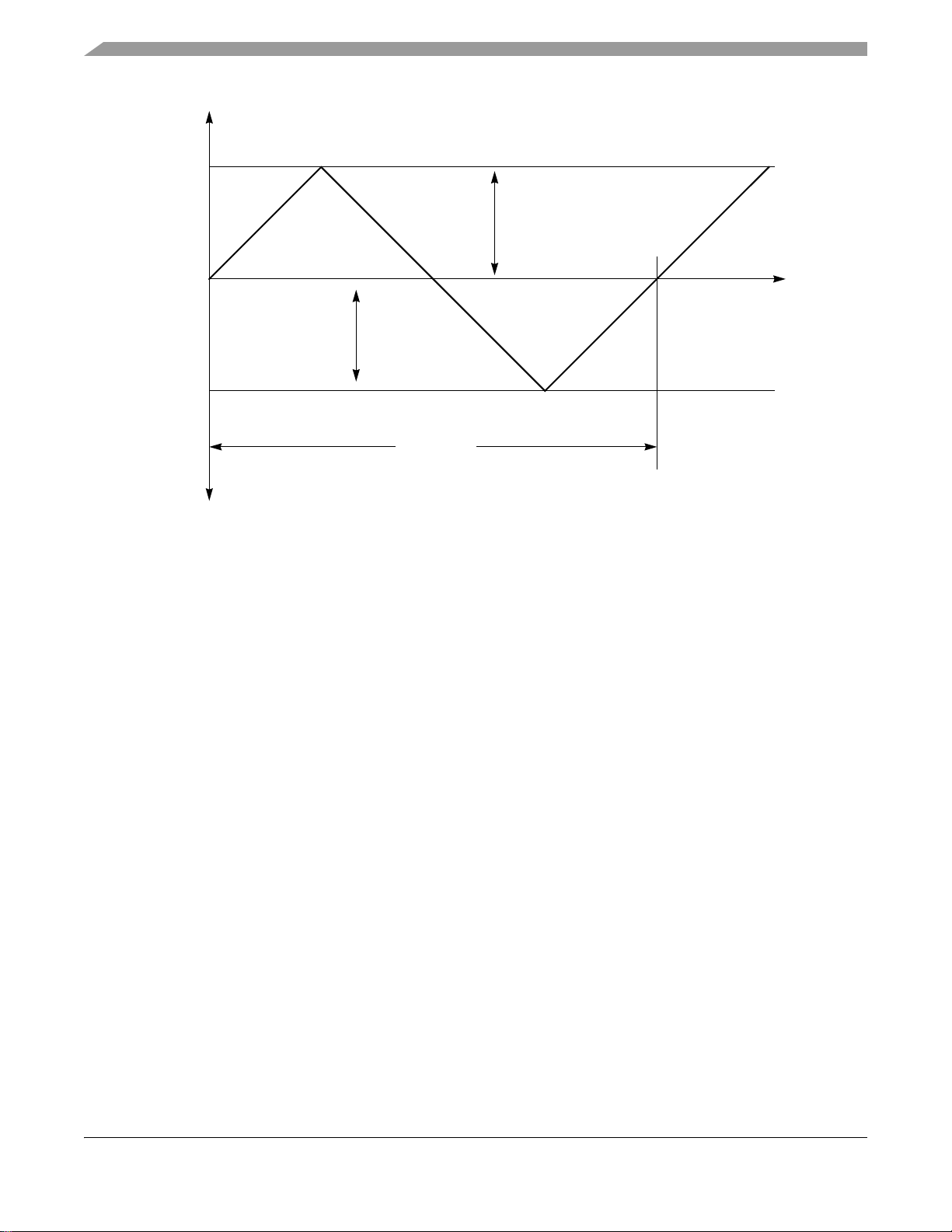
Frequency Modulated Phase Locked Loop (FMPLL)
F
max
F
min
Δt
1
F
mod
--------------
=
t
f
F
max
= F
sys
+ {0.5%, 1%, 1.5%, 2%}
F
min
= F
sys
– {0.5%, 1%,1.5%, 2%}
F
mod
= F
extal
/Q where Q = {20, 40, 80}
ΔFm
ΔFm
Figure 4-6. Frequency Modulation Waveform
4.4.3.4.1 Frequency Modulation Depth Calibration
The frequency modulation calibration system tunes a reference current into the modulation D/A so that the
modulation depth (F
max
and F
) remains within specification. Disable frequency modulation prior to
min
changing the EPREDIV, EMFD, or ERATE bit fields. Upon enabling frequency modulation a new
calibration sequence is performed. A change to EPREDIV, EMFD, or ERATE while modulation is active
will invalidate calibration results.
This routine will correct for process variations, but because temperature can change after the calibration
has been performed, variation due to temperature drift is not eliminated. This system is also voltage
dependent, so if the supply changes after the sequence takes place, error incurred will not be corrected.
The calibration system reuses the two counters in the lock detect circuit, the reference and feedback
counters. The reference counter remains clocked by the reference clock, but the feedback counter is
clocked by the VCO clock.
When the calibration routine is initiated by writing to the EDEPTH bits, the CALPASS and CALDONE
status bits are immediately cleared.
When calibration is induced the VCO is given time to settle before the feedback and reference counters
start counting. Full VCO clock cycles are counted by the feedback counter during this time to give the
initial center frequency count. When the reference counter has counted to the programmed number of
reference count cycles, the input to the feedback counter is disabled and the result is placed in the
COUNT0 register . The calibration system then enables modulation at programmed ΔFm and the VCO gets
time to settle. Both counters are reset and restarted. The feedback counter begins to count full VCO clock
4-16 Freescale Semiconductor
MPC5510 Microcontroller Family Reference Manual, Rev. 1
Preliminary
Page 98

Frequency Modulated Phase Locked Loop (FMPLL)
cycles again to obtain the delta-frequency count. The counter will run only during the high phase of the
triangular modulation waveform. Several half-modulation periods will be measured during the calibration
routine to increase the resolution of the frequency measurement. This will result in a measurement of the
average frequency during the high phase of the modulation waveform which under ideal circumstances
will be equivalent to one-half of the desired modulation depth. When the reference counter has counted to
the new programmed number of reference count cycles, the feedback counter is stopped again.
The delta-frequency count minus the center frequency count (COUNT0) results in a delta count
proportional to the reference current into the modulation D/A. That delta count is subtracted from the
expected value for the selected depth resulting in an error count. The sign of this error count determines
the direction taken by the calibration D/A to update the calibration current. After obtaining the error count
for the present iteration, both counters are cleared. The stored count of COUNT0 is preserved while a new
feedback count is obtained, and the process to determine the error count is repeated. The calibration system
repeats this process eight times, once for each bit of the calibration D/A.
After the last decision is made, a 1 is written to the CALDONE bit of the SYNSR. If an error occurs during
the calibration routine, then CALPASS remains 0. If the routine completed successfully , CALPASS is set
to 1.
4.4.3.4.2 Programming System Clock Frequency With Frequency Modulation
The following steps illustrate proper programming of the frequency modulation mode. These steps ensure
proper operation of the calibration routine and prevent frequency overshoot from the sequence. The PLL
should be programmed and allowed to lock in non-FM mode at the desired frequency as outlined in
Section 4.4.3.3.5, “Programming System Clock Frequency.”
1. Monitor LOCK bit. Do not proceed until the PLL is locked in non-modulation mode.
2. Write a value of ERFD = ERFD + 1 to the ERFD field of the ESYNCR2 to ensure the maximum
system frequency is not exceeded during the calibration routine. This should have been done when
allowing the PLL to lock in non-FM mode.
3. Program the desired modulation rate and depth to the ERATE and EDEPTH fields in the
ESYNCR2. This action initiates the calibration sequence.
4. Allow time for the calibration sequence. Wait for the PLL to lock (i.e. the LOCK bit to set in the
SYNSR). At this time CALDONE should be asserted. CALP ASS will be asserted if the calibration
was successful. If not, the calibration can be re-initiated by repeating from step 3. When the PLL
achieves lock, write the ERFD value desired.
The frequency modulation system is dependent on several factors. The accuracies of the
VDDSYN/VSSSYN voltage, of the crystal oscillator frequency, and of the manufacturing variation.
For example, if a 5 percent accurate supply voltage is used, then a 5 percent modulation depth error will
result. If the crystal oscillator frequency is skewed from the nominal operating frequency, the resulting
modulation frequency will be proportionally skewed. Finally, the error due to the manufacturing and
environment variation alone can cause the frequency modulation depth error to be greater than 20 percent.
MPC5510 Microcontroller Family Reference Manual, Rev. 1
Freescale Semiconductor 4-17
Preliminary
Page 99
Frequency Modulated Phase Locked Loop (FMPLL)
4.5 Resets
This section describes the reset operation of the PLL, including power-on reset and normal resets. The
reset values of registers and signals are provided in other sections.
4.5.1 Clock Mode Selection
The initial clock mode is reflected in the MODE, PLLSEL, and PLLREF bits of the synthesizer status
register (SYNSR) as well as the ESYNCR1[CLKCFG] bit field. The clock mode can be modified by
writing to the CLKCFG bit field. The synthesizer status register will then reflect the newly-selected PLL
clock mode. Table 4-13 shows the clock mode encoding.
The clock mode selection configuration is summarized in Table 4-13.
Table 4-13. Clock Mode Selection
Synthesizer Status Register (SYNSR)
MODE, PLLSEL, and PLLREF Bits
Clock Mode
MODE/
CLKCFG2
Bypass mode 0 X X
Normal mode with external reference 1 1 0
Normal mode with crystal reference 1 1 1
PLLSEL/
CLKCFG1
PLLREF/
CLKCFG0
Reserved 1 0 0
4.5.1.1 Power-On Reset (POR)
The PLL will not operate until the POR signal has negated and the CLKCFG set for PLL mode. Refer to
MPC5510 Microcontroller Family Data Sheet for these thresholds. At this point, the PLL will operate in
self-clocked mode (SCM) until a valid reference clock is detected by the internal clock monitor circuit.
Internal to the PLL, the VCO will be held in reset until the negation of the POR signal. This prevents the
PLL from attempting to lock before its supplies are within specification which can cause VCO/loop gain
to be lower than what the analog loop is designed for.
4.5.1.2 External Reset
After POR has negated, the PLL defaults to Bypass mode and the default clock source for the system clock
is the 16 MHz IRC. After reset exit, the PLL may be configured for operation and after lock may be
selected as the system clock source.
After the initial lock with the default MFD (assuming normal mode was selected), ESYNCR1 may be
written to modify the MFD for the desired operating frequency . The PLL might not lock with an MFD and
crystal frequency combination that attempts to force the VCO outside its operating range.
MPC5510 Microcontroller Family Reference Manual, Rev. 1
4-18 Freescale Semiconductor
Preliminary
Page 100

Frequency Modulated Phase Locked Loop (FMPLL)
CAUTION
When running in an unlocked state, the clocks generated by the PLL are not
guaranteed stable and may exceed the maximum specified operating
frequency of the device. The RFD should always be used as described in
Section 4.4.3.3.5, “Programming System Clock Frequency,” to insulate the
system from any potential frequency overshoot of the PLL clocks.
4.5.2 PLL Loss-of-Lock Reset
By programming the LOLRE bit in the ESYNCR2, the PLL can assert reset when a loss-of-lock condition
occurs. Because the LOCK and LOCKS bits in the SYNSR are re-initialized after reset, the SIU reset status
register (SIU_RSR) (Section 6.3.2.2, “Reset Status Register (SIU_RSR)”) must be read to determine a
loss-of-lock condition occurred.
In PLL Off mode, the PLL cannot lock; therefore a loss-of-lock condition cannot occur and LOLRE has
no affect.
4.5.3 PLL Loss-of-Clock Reset
When a loss-of-clock condition is recognized, RESET is asserted if the LOCRE bit in the SYNCR is set.
The LOCF and LOC bits in the SYNSR are cleared after reset, therefore, the LOC bit must be read in the
SIU_RSR to determine that a loss-of-clock condition occurred. LOCRE has no affect in PLL Off mode.
4.6 Interrupts
This section describes the interrupt requests that the PLL can generate.
4.6.1 Loss-of-Lock Interrupt Request
By setting the LOLIRQ bit in the ESYNCR2, the PLL can request an interrupt when a loss-of-lock
condition occurs.
In PLL Off mode, the PLL cannot lock; therefore a loss-of-lock condition cannot occur and the LOLIRQ
has no affect.
4.6.2 Loss-of-Clock Interrupt Request
When a loss-of-clock condition is recognized, the PLL will request an interrupt if the LOCIRQ bit in the
SYNCR is set. The LOCIRQ bit has no affect in bypass mode or if LOCEN is equal to 0.
MPC5510 Microcontroller Family Reference Manual, Rev. 1
Freescale Semiconductor 4-19
Preliminary
 Loading...